integrated circuit design for radiation sensing and hardening
TRANSCRIPT

Integrated Circuit Design
for Radiation Sensing and Hardening
by
Inyong Kwon
A dissertation submitted in partial fulfillment
of the requirements for the degree of
Doctorate of Philosophy
(Electrical Engineering)
in the University of Michigan
2015
Doctoral Committee:
Professor Dennis M. Sylvester, Co-Chair
Associate Research Scientist Mark D. Hammig, Co-Chair
Professor David Blaauw
Professor David K. Wehe

ii
I dedicate this dissertation to
my honorable parents, precious brothers, dear friends and lovely wife, Jean.
Thanks to their unconditional support, encouragement, and love, this was made possible.

iii
TABLE OF CONTENTS
DEDICATION …...……………………………………………………………………….... ii
LIST OF FIGURES …...………………………………………………………………..... v
LIST OF TABLES ……..………………….…………………………...……………….... ix
CHAPTER
1 Introduction ................................................................................................................... 1
1.1 Recent Trends in Pulse-Processing Units ..................................................... 1
1.2 Circuit Design Challenges ............................................................................ 3
1.3 Scope of the Thesis ....................................................................................... 5
2 Transimpedance Amplifier for Fast Radiation Detection ............................................. 8
2.1 Motivation ..................................................................................................... 8
2.2 Bandwidth Analysis of the Transimpedance Amplifier .............................. 11
2.3 Voltage-Sensitive Preamplifier Design....................................................... 15
2.3.1 Design of the Dual-Inductor TIA ................................................... 15
2.3.2 Input Noise Suppression Technique .............................................. 16
2.3.3 Compensation Technique for Stability .......................................... 19
2.3.4 Equivalent Noise Analysis ............................................................. 20
2.4 Chip Implementation Details ...................................................................... 23
2.5 Measurement Results .................................................................................. 24
2.5.1 Electrical Characteristics ............................................................... 24
2.5.2 Radiation Source Measurement and TIA Comparison .................. 26
2.6 Summary ..................................................................................................... 28
3 Detector Capacitance Compensation Preamplifier ..................................................... 29
3.1 Motivation ................................................................................................... 29
3.2 Integrated Circuit Design ............................................................................ 32
3.2.1 Miller Effect ................................................................................... 34
3.2.2 Design of Unity-Gain Amplifier .................................................... 34

iv
3.2.3 Design of Charge-Sensitive Amplifier .......................................... 36
3.3 Chip Implementation Details ...................................................................... 38
3.4 Simulation Results ...................................................................................... 40
3.4.1 Transient Analysis of Charge-to-Voltage Gain and Rise Time ..... 40
3.4.2 Noise Analysis ............................................................................... 44
3.5 Radiation Detectors ..................................................................................... 44
3.5.1 Fabrication and Structure ............................................................... 44
3.5.2 Capacitance Comparison of the Sensor ......................................... 47
3.6 Measurement Results .................................................................................. 50
3.6.1 Validation for Detector Capacitance Compensation ..................... 50
3.6.2 Analysis on Resolution and Energy Loss in Air ............................ 53
4 Razor-Lite: A Light-Weight Register for EDAC........................................................ 57
4.1 Motivation ................................................................................................... 57
4.1.1 View of Radiation-Hardened-by-Design ....................................... 57
4.1.2 View of Variation Tolerant Processor ........................................... 59
4.2 Design Overview ........................................................................................ 63
4.2.1 Razor-Lite Core Circuit ................................................................. 63
4.2.2 Duty-Cycle Controller ................................................................... 67
4.2.3 Metastability Considerations ......................................................... 72
4.2.4 Virtual Rail Leakage ...................................................................... 75
4.2.5 Low Voltage Operation ................................................................. 75
4.3 Chip Implementation Details ...................................................................... 76
4.4 Measurement Results .................................................................................. 79
4.4.1 Energy Efficiency .......................................................................... 80
4.4.2 Critical Path Analysis .................................................................... 85
5 Conclusion and Contributions .................................................................................... 87
BIBLIOGRAPHY ……..………………….…………………………....……………...… 91

v
LIST OF FIGURES
Figure 1. 1: Trends in size scaling of transistors. Evolution of MOSFET gate length in production-
stage integrated circuits (filled red circles) and International Technology Roadmap for
Semiconductors (ITRS) targets (open red circles). [1] .................................................. 2
Figure 1. 2: (a) Simplified circuit model of a radiation detector with the intrinsic capacitance, CD.
(b) Readout structure with a charge-sensitive preamplifier, and (c) a voltage-sensitive
preamplifier. ................................................................................................................... 5
Figure 2. 1: The voltage-sense amplifier replacing the traditional readout configuration for high
speed radiation detection system. ................................................................................. 10
Figure 2. 2: Feedback structure of a transimpedance amplifier with the circuit model of a diode. 12
Figure 2. 3: Transfer functions of the op-amp, A(s) and the feedback component, β for graphical
analysis. ........................................................................................................................ 13
Figure 2. 4: Schematic of the voltage-sensitive preamplifier with TIA and buffer. ....................... 16
Figure 2. 5: (a) Two major noise sources contributing to input referred current noise from TIA. (b)
Conceptual input current noise spectral density function vs. frequency. ..................... 17
Figure 2. 6: (a) A series LC circuit to suppress the input current noise through Zin. (b) Completed
structure of the voltage-sensitive amplifier for noise suppression and bandwidth
enhancement. ................................................................................................................ 18
Figure 2. 7: Stability simulation results of the feedback system. Phase margin is 66.370 at 0 dB
open loop gain. ............................................................................................................. 20
Figure 2. 8: Equivalent noise analysis circuit including feedback resistor, input impedance of the
TIA and induced gate noise source. ............................................................................. 21
Figure 2. 9: Gate induced input current noise simulation of the TIAs w/ (red line) and w/o (blue
line) inductors............................................................................................................... 23
Figure 2. 10: Die photo and wire-bonded chips on a printed circuit board for testing. .................. 24
Figure 2. 11: Measured frequency responses with different inductors. .......................................... 25
Figure 2. 12: Measured frequency responses with different input capacitance. ............................. 26
Figure 2. 13: NaI(Tl)-PMT energy spectrum of the 662 keV photopeak from 137
Cs, derived from a
measurement chain employing either a charge-sensitive amplifier (Ortec 113) or the

vi
dual-inductor TIA. The measurement period for each spectrum was 900 s. Note that
the spectrum derived from the Ortec 113 is shifted to the right by 5 keV for clarity. . 27
Figure 2. 14: NaI(Tl)-PMT energy spectrum of the 662 keV photopeak from 137
Cs, derived from a
measurement chain employing either the baseline TIA (without inductors) or the dual-
inductor on-chip TIA. The spectra shifts to higher channels due to the enhanced gain
and bandwidth. ............................................................................................................. 27
Figure 3. 1: Traditional charge-sensitive amplifier with a radiation detector model. Charges
produced by the detector are shared between the detector and feedback capacitances,
affecting the gain of the front-end readout circuit. ...................................................... 31
Figure 3. 2: Configuration with a charge-sensitive preamplifier and a unity-gain amplifier to
compensate the detector capacitance. .......................................................................... 33
Figure 3. 3: Circuit diagram of the Miller Effect which is applied to the unity-gain amplifier in
order to seemingly have zero detector capacitance for the downstream readout circuits.
...................................................................................................................................... 35
Figure 3. 4: Unity-gain amplifier design with a unity-gain operational amplifier. ......................... 35
Figure 3. 5: Voltage transfer function of the unity-gain amplifier. ................................................. 36
Figure 3. 6: Charge-sensitive amplifier design with a two-stage operational amplifier including a
current mirror. .............................................................................................................. 37
Figure 3. 7: Voltage transfer function of the charge-sensitive amplifier. ....................................... 37
Figure 3. 8: (a) Closed-loop gain and (b) phase transfer functions of the charge-sensitive amplifier
with feedback components. Phase margin of 84⁰ is shown. ........................................ 38
Figure 3. 9: (a) Die photo and (b) wire-bonded chips on a printed circuit board for testing. ......... 39
Figure 3. 10: Ten thousand Monte Carlo simulations of the charge-to-voltage gain (top) and rise
time (bottom) at the output indicate that the readout system is robust against process,
voltage and temperature variations. ............................................................................. 41
Figure 3. 11: (a) Frequency and (b) transient responses of the charge-sensitive amplifier without
the technique. Charge-to-voltage gain is dramatically reduced by detector capacitance
increase for a standard CSA. ........................................................................................ 42
Figure 3. 12: (a) Frequency and (b) transient responses of the charge-sensitive amplifier with the
technique. Charge-to-voltage gain is preserved even though detector capacitance
increases. ...................................................................................................................... 42
Figure 3. 13: Charge-to-voltage gain and rise time at the output of the charge-sensitive amplifier
are maintained as the detector capacitance increases. .................................................. 43
Figure 3. 14: (a) Total output noise is increased with detector capacitance. Nevertheless, (b) the
SNR is much higher for the unity-gain amplifier than for the preamplifier without the
technique. ..................................................................................................................... 45
Figure 3. 15: Two silicon radiation sensors (a) and (b) have different detector capacitance of 0.65
pF and 16.25 pF used for verifying the detector capacitance compensation technique.
...................................................................................................................................... 45
Figure 3. 16: Schematic of the fabrication processes for the pin type Si detector. ......................... 47

vii
Figure 3. 17: Analytic capacitance comparison for the effect of the fringe capacitance. ............... 49
Figure 3. 18: Junction capacitance estimated from the formula comparison with the C-V measured
capacitance. .................................................................................................................. 49
Figure 3. 19: Alpha particle spectra of 241
Am measured by small and large area silicon detectors.
...................................................................................................................................... 51
Figure 3. 20: Alpha particle spectra of 241
Am measured by the small area silicon detector with and
without the detector compensation technique. ............................................................. 52
Figure 3. 21: Alpha particle spectra of 241
Am measured by the large area silicon detector with and
without the detector compensation technique. The channel number located in the peak
is dramatically increased by the technique................................................................... 52
Figure 3. 22: Comparison between experimental data (three sets) for alpha energies from 241Am
in air as well as the calculations from ICRU data (dashed line), SRIM data (solid line)
and SRIM data x 0.95 (dotted line) [53]. .................................................................... 54
Figure 3. 23: Three stands of 3.3, 2.5, and 2.2 cm placed in a testing box for analyzing alpha
energy loss in air. ......................................................................................................... 54
Figure 3. 24: Alpha particle spectra of 241
Am measured by the large area silicon detector (a)
without and (b) the detector compensation technique. The spectra were measured on
three stands to address alpha energy loss in air............................................................ 55
Figure 3. 25: Reduced energy particles vs. resolution. The resolution gets better beyond 2.15 MeV
particles by applying the detector capacitance compensation technique. .................... 56
Figure 4. 1: A logic stage and registers in a clock based digital circuit (left). Traditional D Flip-
Flop schematic diagram (right). ................................................................................... 58
Figure 4. 2: (a) Clock period histogram and (b) fraction of registers by delay slack for an ARM
Cortex-M3 processor [73], [74]. .................................................................................. 62
Figure 4. 3: Overhead ratio comparisons of three ARM Cortex-M3 variants; a) baseline, without
EDAC, b) with 20% insertion of EDAC registers from [68], c) with 20% insertion of
Razor-Lite registers. ..................................................................................................... 63
Figure 4. 4: Conventional DFF schematic and added Razor-Lite monitoring circuit. .................... 65
Figure 4. 5: Razor-Lite timing and error detection waveforms showing error signals being
generated from virtual rail transitions during high clock phase. .................................. 65
Figure 4. 6: Conceptual timing diagram for required speculation window to manage hold time
constraint issue and late arrival signal detection in the Razor scheme by detecting and
correcting errors. .......................................................................................................... 69
Figure 4. 7: (a) Schematic of the tunable pulse generator used for duty cycle control; (b) statistical
sampling circuit for measuring duty cycle. .................................................................. 70
Figure 4. 8: Calibration sequences to dynamically tune duty cycle for maximum speculation
window while avoiding the flagging of errors due to fast paths. ................................. 71
Figure 4. 9: Measurement results show that tuning duty cycle has a large impact on error rates and
overall system performance/efficiency. ....................................................................... 72

viii
Figure 4. 10: Timing diagrams showing the transient behavior of Razor-Lite in response to both
long-term (Cases 1 and 2) and short-term (Cases 3 and 4) metastable events at DN. . 74
Figure 4. 11: One million Monte Carlo DC simulations of the voltage difference between
monitoring circuit switching threshold (VT, for each VVSS at left and VVDD at right)
and metastable voltage level of node DN. Results indicate that substantial margin
exists to avoid metastability. ........................................................................................ 74
Figure 4. 12: System block diagram of Razor-Lite implemented in an Alpha 64 architecture
processor, including error aggregation and controller, as well as half-speed clock
generator for error mitigation. ...................................................................................... 77
Figure 4. 13: Timing diagram shows the behavior of the system when an error occurs; taken
together an error incurs an 11 cycle performance penalty. .......................................... 77
Figure 4. 14: Die photograph of Razor-Lite core and implementation details of chip. .................. 79
Figure 4. 15: Measured results from a typical die at 25°C show 83% energy efficiency
improvement (45.4% energy reduction) of Razor-Lite core compared to a margined
baseline core (1.1V, 85°C, 2σ process). ....................................................................... 81
Figure 4. 16: Total error count and the number of registers with errors at 25°C and 1.2 GHz. ...... 82
Figure 4. 17: Highly critical registers from measured results compared to final post-extracted
timing analysis predictions. .......................................................................................... 82
Figure 4. 18: Measured PoFF of the slowest, typical, and fastest dies across temperature. ........... 84
Figure 4. 19: Percentage energy reduction compared to the worst PoFF voltage chip from 29 chips
for all chips running at 25°C. ....................................................................................... 84
Figure 4. 20: Measured path delay changes according to voltage scaling. Paths below 1 indicate
that their delay become faster at low voltage. These paths exhibit a possibility of
violating hold time when voltage scaling. ................................................................... 86

ix
LIST OF TABLES
Table 3. 1: Charge-to-voltage gain and rise time with the technique at the best and worst statistical
model. One sigma standard deviations are also tabulated............................................ 41
Table 3. 2: Capacitance of the 2 mm and 10 mm diameter circular diode from the C-V
measurement ................................................................................................................ 50
Table 4. 1: Razor-Lite register delay, energy, and area overhead compared to a traditional DFF, as
determined by SPICE simulation including layout parasitics. ..................................... 67
Table 4. 2: Measured energy efficiency for slow/typical/fast dies using Razor-Lite. .................... 81
Table 4. 3: Comparison chart of Razor-Lite and previous ECAD works. ...................................... 86

1
CHAPTER 1
Introduction
1.1 Recent Trends in Pulse-Processing Units
Since the mid-twentieth century, the integrated circuit (IC) has been gradually developed
and widely used in numerous electronic devices such as personal computers (PCs), cell phones,
medical equipment and military equipment. The development of IC technologies has reduced the
design and production costs as well as increased reliability of the final products encompassed in
single packages thereby reducing their size while minimizing connection problems and assembly
errors. These advantages have been maximized by continuously developing lithographic
techniques that can reduce the size of a single transistor as shown in Figure 1.1. Today, digital
processors contain more than two billion transistors with gate lengths of just 20 nm. This size
scaling leads to significant changes in electronic instruments containing ICs, especially those
deployed for measurement applications.
In the radiation measurement field, most electronic instrumentation was developed in the
context of vacuum tube circuits developed during the twentieth century. For mounting pulse-
processing units in a vertical stack, this equipment was adjusted to fit a frame in a standard 19-in.
relay rack. The two international standards, the Nuclear Instrumentation Module (NIM) and

2
Figure 1.1: Trends in size scaling of transistors. Evolution of MOSFET gate length in
production-stage integrated circuits (filled red circles) and International Technology Roadmap
for Semiconductors (ITRS) targets (open red circles). [1]
the Computer Automated Measurement And Control (CAMAC) [2]–[4], that fit into the full 19-
in. housing called a bin or crate, are the most widely used nuclear electronics form factors. Even
though all electronics continue to be manufactured in the full 19-in. width and widespread use
persists to this day for mounting of nuclear electronic components conveniently, the advent of
solid-state circuitry has led to much more compact size occupied by a single chip.
The demand of application specific integrated circuits (ASICs) in radiation measurement
applications is rapidly increasing for compact and portable experiments since semiconductor
detectors have undergone continuous development for several decades [5] and recently become
more popular due to their unique properties that include: a) high speed and precise position
sensing with readout ICs, b) direct and efficient charge conversion, c) the possibility of

3
integrating the detector and the readout circuit on the same silicon substrate, and d) low
fabrication cost in mass production. In this transition period, ASICs for radiation detection can
carry out essential functions such as signal comparison, amplification, and data acquisition.
Moreover, thanks to the small scale of ICs, a number of parallel channels of readout systems can
be built in a single chip while the traditional standards are too bulky to be compactly integrated
for multi channel detectors; for example, pixelated detectors where independent readout circuits
are required for each output.
1.2 Circuit Design Challenges
For several decades, the front-end receiver topology, consisting of a charge-sensing
preamplifier and a shaping amplifier, has been developed and used for signal processing in
nuclear radiation measurement applications. However, the signal acquisition time of the
traditional signal processing chain has remained a chronic problem due to the integration of the
RC-CR filtering in the shaping amplifier. This relatively slow signal processing increases the
probability of pulse pile-up and inaccurate data acquisition during measurements. Most
pressingly, semiconductor-based nuclear radiation detectors require a wide bandwidth and low
input noise preamplifier because small current pulses are extracted following the interaction of
quanta from radiation sources, such as alpha particles and gamma-rays. Ideally, one would prefer
to detect the 10’s of picoamps that accompanies the motion of a single carrier in a depleted
semiconductor. In general, hundreds to many thousands of charges are generated in a
semiconductor detector and subsequently transported to the collecting electrodes in nanosecond
time-frames [6]. Thus, nanoampere to microampere sensing is desired from the front end circuit
accompanied by both low input-noise and wide bandwidth performance.

4
In addition to the detection speed issue, the capacitance of the radiation detector is also a
major hindrance to a following readout system, especially for large area detectors or for those
semiconductor sensors derived from high permittivity materials such as PbSe [7]. As shown in
Figure 1.2, this unwanted detector capacitance can degrade the voltage gain and increase the
noise during pulse formation. Generally, in a charge-sensitive preamplifier structure of Figure
1.2 (b), charges generated from detectors are accumulated in the feedback capacitor CF, which
determines the value of the output voltage signal according to the size of CF and the amount of
the generated charge, Q. For ideal data acquisition, all of the flowing charges should accumulate
upon CF to derive full information from an interaction; however, in practice, some are shared
with the parasitic capacitance, CD. This results in gain loss at the output of the preamplifier. Even
though a voltage-sensitive amplifier scheme is used for converting charges directly to voltage as
shown in Figure 1.2 (c), the intrinsic capacitance CD significantly affects the bandwidth and
noise of the signal processing unit. The reduced bandwidth causes poor linearity and information
loss in the high frequency region. Consequently the intrinsic capacitance of radiation detectors
should be minimized during manufacturing. However, some detector materials, for instance
nanocrystalline semiconductors, naturally possess a large intrinsic capacitance because the
relative permittivity of a lead-chalcogenide based nanodetector is about 100 times larger than
that of silicon-detectors. That is, the noise level is increased 10 times because the noise charge is
proportional to the square root of the capacitance. Although one can make a small contact upon a
large semiconducting volume to mitigate the effect of the detector capacitance, one cannot
always tolerate the longer drift times associated with such a design. Therefore, we have come up
with a technique to overcome this issue via the readout circuit design.

5
Detector Bias
Vout
CDIS
Preamp
Vout
-
+
Op-amp
CF
Radiation Detector
CDIS
Radiation Detector
Detector Bias
Q
Vout
-
+
Op-ampCDIS
Radiation Detector
Detector Bias
Q
RF
(a) (b) (c)
Figure 1.2: (a) Simplified circuit model of a radiation detector with the intrinsic capacitance, CD.
(b) Readout structure with a charge-sensitive preamplifier, and (c) a voltage-sensitive
preamplifier.
Finally, radiation hardening is also a big challenge for circuit designers in this field. In
addition to conventional applications, electronic devices are also necessary components in
various scientific, military, and space sensing systems that are exposed to high radiation
environments. In contrast to conventional commercial applications, a radiation-hardened-by-
design (RHBD) technique is required to protect circuits from radiation effects in those
applications. Incident ionizing radiation impacting a node in an electrical circuit and generating
additional and unpredicted charges is called a single-event effect (SEE). This non-destructive
SEE can affect digital logic blocks in a circuit by flipping the data state, a condition known as a
single-event upset (SEU) [8]–[11]. Since most computing processors for data analysis have a
number of digital blocks including storage cells in their architectures, SEEs can produce
significant malfunctions to a system that includes radiation intolerant circuits. Therefore, refined
RHBD techniques are needed for radiation-tolerant applications.
1.3 Scope of the Thesis
This dissertation discusses several major circuit blocks required in radiation measurement

6
applications. These circuits attempt to resolve rising issues as mentioned in this chapter,
addressed by particular circuit techniques. The remainder of the thesis is outlined below.
In Chapter 2, a high gain transimpedance amplifier (TIA) with a gate noise suppression
technique is discussed. High-speed pulse shape analysis using the preamplifier can allow one to
extract the physical parameters that govern a radiation’s interaction. This chapter presents a
voltage-sensitive preamplifier that can replace conventional configurations that contain a charge-
sensitive preamplifier and shaping amplifier chain, especially for high speed radiation
measurement systems. A transimpedance amplifier is a primary circuit of the preamplifier design
based on a feedback structure with cascade inverting amplifiers and a feedback resistor, but one
that incorporates a bandwidth and gain enhancement technique that utilizes a series LC circuit at
the input of the amplifier. This configuration is designed to reduce the size, power consumption,
and complexity of the front-end circuitry traditionally used in radiation measurements, while
enhancing pulse-shape analyses by preserving the temporal information of the carriers following
radiation impingement.
In Chapter 3, a technique by which compensates for the detector capacitance using the
Miller Effect is discussed. This chapter describes an integrated circuit design for a modified
charge-sensitive amplifier (CSA) that compensates for the effect of capacitance presented by
nuclear radiation detectors and other sensors. For applications that require large area
semiconductor detectors or for those semiconductor sensors derived from high permittivity
materials such as PbSe, the detector capacitance can degrade the system gain and bandwidth of a
front-end preamplifier, resulting in extended rise times and attenuated output voltage signals
during pulse formation. In order to suppress the effect of sensor capacitance, a unity-gain
amplifier was applied into a traditional CSA. The technique exploits the Miller Effect by

7
reducing the effective voltage difference between the two sides of a radiation detector which
minimizes the capacitance presented to the differential common-source amplifier. This new
configuration is successfully designed to produce effective gain even at high detector
capacitance. The entire circuit, including a core CSA with feedback components and a unity-
gain amplifier, are implemented in a 0.18 μm CMOS process with a 3.3 V supply voltage.
In Chapter 4, a light-weight register design for error detection and correction is discussed.
This chapter presents Razor-Lite [12], [13], which is a low-overhead register for use in error
detection and correction (EDAC) systems. These systems are able to eliminate timing margins by
using specialized registers to detect setup time violations as well as SEE. However, these EDAC
registers incur significant area and energy overhead, which mitigates some the system
benefits. Razor-Lite is a new EDAC register that addresses this issue by adding only 8
additional transistors to a conventional flip-flop design. The Razor-Lite flip-flop achieves low
overhead via a charge-sharing technique that attaches to a standard flip-flop without modifying
its design. Side-channels connected to the floating nodes generate error flags through simple
logic gates totaling 8 transistors, enabling register energy/area overheads of 2.7%/33% over a
conventional DFF, while also not incurring extra clock or datapath loading or delay. Razor-Lite
is demonstrated in a 7-stage Alpha architecture processor in a 45nm SOI CMOS technology with
a measured energy improvement of 83% while incurring a 4.4% core area overhead compared to
a baseline design.
Finally, Chapter 5 concludes the dissertation with future work.

8
CHAPTER 2
Transimpedance Amplifier for Fast Radiation Detection
2.1 Motivation
Homeland security and medical imaging applications require portable and fast radiation
detection systems that possess small system size and low power consumption while maintaining
spectroscopic performance. To satisfy the requirements, application specific integrated circuit
(ASIC) technologies have been developed and used that employ the traditional front-end receiver
topology that consists of a charge-sensitive preamplifier and a shaping amplifier [5], [14], [15].
Although many researchers have focused on reducing the noise from the readout ASICs to yield
better performance in terms of resolution [16]–[23], boosting the signal acquisition speed
requires further improvement because of the temporal delays associated with the charge
integration time in the charge-sensitive amplifier and the filtering of the output voltage signal in
a shaping amplifier. Despite the efforts to reduce the charge integration time of a charge-
sensitive amplifier by applying a fast rise-time technique [24] or by using a dynamic slew
correction circuit [25], the pulses generated from these topologies are still measured in the
dozens of microsecond range.

9
In [26], the authors present an alternative architecture with a current-current amplifier for
the front-end receiver, but the bandwidth is only 90 MHz. This relatively slow signal processing
through the charge-sensitive and shaping amplifiers increases the probability of pulse pile-up and
inaccurate data acquisition during measurements.
In contrast, a voltage-sensitive amplifier as shown in Figure 2.1 can potentially replace the
preamp-shaper modality with a single component, a transimpedance amplifier (TIA) that directly
converts charges to voltage signals while reducing the area overhead and power consumption
with fast signal processing if it has sufficiently large gain and bandwidth to accurately amplify
the small current signals generated following radiation-impact events.
Semiconductor-based nuclear radiation detectors require a wide bandwidth and low input-
noise TIA because small current pulses are extracted following the interaction of quanta from
radiation sources. Ideally, one would prefer to detect the tens of picoamperes that accompany the
motion of a single carrier in a depleted semiconductor such as silicon. In general, hundreds to
many thousands of charges are generated in the active region and subsequently transported to the
collecting electrodes in nanosecond time-frames [6]. Thus, nanoampere to microampere sensing
is desired from the front end circuit accompanied by both low input noise and wide bandwidth
performance.
For scintillator-based detectors, the photomultiplier tube provides ample gain to sense
radiation impact events; however, for high-rate counting applications and large-volume
scintillators, pulse pile-up can degrade the imaging capability of the device. For instance, we are
developing a depth and angular sensitive gamma-ray camera for neutron-interrogated materials,

10
Charge-sense Amp Shaping Amp(RC-CR filter) SpectrumRadiation Detector
Voltage-sense Amp SpectrumRadiation Detector
Figure 2.1: The voltage-sense amplifier replacing the traditional readout configuration for high
speed radiation detection system.
focusing on the localization and identification of conventional high-explosives [27], [28].
Extending the imaging range to 10’s of meters requires high neutron source intensities and large
volume detectors, in an instrument that must be deployed upon a mobile, vibratory platform [29].
In this work an inductive peaking technique for enhancing the bandwidth introduces
resonant peaking in the amplitude, rolling off near the highest frequencies in the passband [30]–
[32]. However, the extended bandwidth induced by the inductive peaking technique is prone to
instability, to a degree depending on the parasitic capacitance of the radiation sensor. Therefore,
the TIA has an additional inductor inserted at the front of the device to ensure stability of the
system and suppress the induced gate noise for better performance.
In the following sections, we present a TIA design as a voltage-sensitive amplifier providing
large enough gain and bandwidth for radiation detectors. The electrical performance of the TIA
is quantified and its utilization in a scintillator-based gamma-ray measurement is demonstrated.
The results confirm that compact and fast readout systems can be implemented and integrated for
the next generation of radiation detection systems.

11
2.2 Bandwidth Analysis of the Transimpedance Amplifier
The conventional TIA topology consists of an op-amp, a shunt feedback resistor RF, and a
shunt feedback capacitor CF for increased stability as shown in Figure 2.2. The output voltage
transfer function is simply defined [33]:
. (2.1)
Its function is to convert an input current signal to an output voltage signal based on Ohm’s
Law: IS∙ZF, where ZF, the cut off frequency, is 1/(2πRFCF). However, designing a TIA with a
feedback loop is delicate and prone to oscillation due to phase shifts. In addition, the above
equation does not consider the intrinsic resistance and capacitance of the photodiode and
assumes an ideal op amp with infinitely large gain-bandwidth product (GBW). Therefore, a more
thorough analysis for the design of the feedback system is required.
With a more accurate model of a TIA including a photodiode, the transfer function of the
closed-loop gain is:
(2.2)
. (2.3)
The gain in the low frequency region is 1 when the intrinsic resistance RD of the photodiode
is larger than RF. This means that a certain input voltage does not affect the output voltage

12
Radiation Detector
(e.g. photodiode)
Vout
RF
-
+
CF
RDCDIS
β =ZF
Op-amp
A(s)
Figure 2.2: Feedback structure of a transimpedance amplifier with the circuit model of a
radiation detector as a diode.
because the circuit operates as a current-to-voltage amplifier (voltage-sensitive amplifier).
In a general feedback system, an analysis of the open-loop gain that results in instability
when |A(s) β| =1 with the phase shift of -360⁰ should be considered to ensure that the TIA stable.
For the open-loop analysis of a feedback system, transfer functions of an op-amp gain A(s) and a
closed-loop gain 1/ β are depicted in Figure 2.3. At the crossing point between A(s) and 1/ β the
TIA will oscillate since |A(s) β| = 1 with a phase shift of -360⁰ including two poles from the op-
amp and β, since the zero, fZ, of 1/β produces the phase shift of -90⁰ and the op-amp generally
has the phase shift of -180⁰ as an inverting amplifier. However, setting up the compensation
zero, fP, which is the pole of 1/β, cancels out -90⁰ and makes the TIA stable. If fP lies at fP2 inside
the curve of A(s), it is stable but it degrades the bandwidth of the TIA because the 3 dB
bandwidth of the TIA is decided by the pole, fP.

13
A(s)
Log Av
Log f
1 / β
fZ fP2 fP3 fP1 GBW
1
Figure 2.3: Transfer functions of the op-amp, A(s) and the feedback component, β for graphical
analysis.
In order to obtain the best value fP3, the compensation feedback capacitor, CF can be
obtained by geometrical analysis in Figure 2.3 and (2.2). The closed-loop gain in the high
frequency region is:
. (2.4)
At the crossing point, the overall gain of the TIA is |A(s) β| = GBW/fP3 which is the closed-
loop gain calculated by (2.4):
. (2.5)
In Figure 2.3, fP3 is exactly in the middle of two curves following 20 dB/decade slopes.
Thus,

14
(2.6)
where fZ is calculated from ACL and GBW/fP3 yields:
. (2.7)
This equation indicates how to select an appropriate feedback capacitor to prevent an
oscillation for a stable TIA. On the other hand, if a large RF is required due to small input
currents into the TIA in the range of a few microamperes such as for the nuclear measurement
application, CF can be safely ignored as was done for the dual-inductor design. Finally, the
overall bandwidth of TIA calculated by ZF and (2.6) becomes:
. (2.8)
This final equation (2.8) indicates that a more accurate expression for the bandwidth of the
TIA is considerably different from the simple bandwidth 1/2πRFCF of (2.1). Understandably, a
TIA designed with the simplified equation is prone to oscillate and trouble circuit engineers in
many cases. As shown above, the GBW of the op-amp is the only parameter needed to improve
the bandwidth of the total system when CD and RF are fixed by a detector and a desired
transimpedance gain, respectively.

15
2.3 Voltage-Sensitive Preamplifier Design
Voltage-sensitive amplifiers are generally implemented in the front ends of receivers to
directly convert charges generated by photomultipliers or photodiodes to a voltage signal [33]
whereas charge-sensitive amplifiers typically utilize an additional shaping amplifier to improve
the SNR of the signal. In order to realize a compact front-end receiver, we have designed for: (a)
a large gain and bandwidth, and (b) an allowable input current noise for transforming small
current signals from the detectors. In exploiting the inductive peaking technique, the TIA
successfully resolves the issues by improving the system gain and bandwidth as well as reducing
the input current noise with a series LC circuit at the front end of the TIA.
2.3.1 Design of the Dual-Inductor TIA
Figure 2.4 shows the circuit architecture of the TIA. The system bandwidth can be obtained
from feedback circuit analysis, as discussed in Chapter 2.2 where the variables are defined in
(2.8). The system requires not only a large bandwidth, BWTIA of approximately 1 GHz to
transform nanosecond wide signals but it also needs a large transimpedance gain, RF, in the
kilohm range to detect the miniscule current pulses that can be generated in semiconductor
sensors [6]. To satisfy these two conflicting variables, three stages of cascaded common-source
(CS) amplifiers were implemented to increase the gain-bandwidth product (GBW).
According to (2.8), a poly-silicon on-chip resistor RF of 11 kΩ, realized through the
feedback loop must be compensated by a correspondingly large GBW of the CS amplifiers in
order to maintain the gigahertz bandwidth of BWTIA. For the large GBW of the core amplifier, a
three-stage CS amplifier is used that presents a gain and bandwidth of 10.42 dB (= 3.32) and
13.165 GHz, respectively. The overall GBW of the CS amplifiers is therefore 43.65 GHz. In

16
Radiation
Detector
TIA+Buffer
Current
Scope
Voltage
RF
L1L2In Out
Vbias_Buffer
TIA Buffer
Figure 2.4: Schematic of the voltage-sensitive preamplifier with TIA and buffer.
addition to the three-stage amplifier, two inductors are added at the front-end of the TIA to
enhance the bandwidth of the overall TIA by inductive peaking. Finally, a CS amplifier and a
source follower, acting as a buffer, are placed after the TIA for 50 Ω matching to down-stream
readout circuits.
2.3.2 Input Noise Suppression Technique
In a conventional TIA with a feedback resistor as shown in Figure 2.5 (a), there are two
major noise sources: thermal noise from the resistor and gate noise from the first stage transistor
[34]. One of them, the thermal noise of the feedback resistor adds only a small contribution to
the input referred current noise in the high frequency region because the thermal noise is

17
Vout
Thermal noise
Gate noise f
Thermal+Shot noise
Gate noise
1/f noise
RF
Photodetector
f
2
ngI
(a) (b)
Figure 2.5: (a) Two major noise sources contributing to input referred current noise from TIA.
(b) Conceptual input current noise spectral density function vs. frequency.
commonly a white Gaussian noise and flat versus frequency. Moreover, the current thermal noise
power spectral density (PSD) is inversely proportional to the resistance which is quite small
when a large feedback resistor is employed to amplify a small input current. The gate noise is
defined by the induced thermal noise from the drain and the shot noise from the channel,
respectively [35]:
,
. (2.9)
Among these two current noise sources, the induced drain noise is dominant because the
noise is a quadratic function of frequency, as depicted schematically in Figure 2.5 (b). Generally,
the noise rapidly increases at frequencies beyond the gigahertz range.
In order to reduce the gate noise from the first-stage transistor, an on-chip inductor
exploiting the properties of a series LC circuit which has theoretically zero impedance at the

18
RF
Vout
Photodetector
CDIS
CgsZin
L1RF
Zopen
CD
Zopen
L1
RF
Vout
Photodetector
CDIS
Zopen RF
Zopen
CD
L1L2
Cgs
L1L2
Cgs
(a)
(b)
Figure 2.6: (a) A series LC circuit to suppress the input current noise through Zin. (b) Completed
structure of the voltage-sensitive amplifier for noise suppression and bandwidth enhancement.
resonant frequency is implemented, as shown in Figure 2.6 (a). The inductor L1 in series with the
gate capacitance forms a series LC tank and the impedance, Zin is defined:
, (2.10)
where R is an intrinsic resistance of the inductor and the gate. Although this parasitic resistance
reduces the quality factor Q = ω0L/R, which determines the deepness of the noise suppression at
the resonant frequency, the series LC circuit reduces the gate noise contribution to the input
referred current noise at the resonant frequency which should be set at the 3 dB bandwidth of the

19
TIA. However, the inductor added at the input node forms a parallel LC tank with the inherent
capacitance of the radiation detector, CD which can cause instability.
2.3.3 Compensation Technique for Stability
In evaluating the system stability, the impedance Zopen consisting of the inductor and CD in
Figure 2.6 (a) is obtained by:
. (2.11)
where the symbol ‘||’ borrows the parallel lines notation from geometry, e.g. A||B = AB/(A+B).
The open loop gain peaking and the phase drop of -180⁰ due to the parallel LC circuit at the
resonant frequency causes a fatal stability issue that can induce TIA oscillations. In order to
cancel this negative effect one more inductor, L2 is added in series with CD as shown in Figure
2.6 (b). Intuitively, the additional inductor forms a series LC tank with CD and cancels out the
gain peaking and phase shift of the open loop path in a stability analysis because a series LC
circuit has a negative gain peaking and a phase shift of +180⁰. Therefore the value of the second
inductor should be carefully chosen in accordance with the equation below:
. (2.12)

20
Phase Margin of 66.371
100
50
0
-50
-100
Deg
ree
40
0
-40
dB
106 107 109 1010
Loop Gain Phase
Loop Gain dB20
Frequency (Hz)108
Figure 2.7: Stability simulation results of the feedback system. Phase margin is 66.370 at 0 dB
open loop gain.
If L2 is the value that satisfies L1Cgs = L2CD, then all second order terms of s in (2.12) are
canceled. The stability simulation results of the dual-inductor TIA in Figure 2.7 shows that the
circuit is stable with the phase margin of 660 at 0 dB open loop gain in a feedback topology.
2.3.4 Equivalent Noise Analysis
The resolution of a readout system is directly related to the circuit noise if a detector/sensor
shows high performance with lower noise than a following preamplifier. For those high-
resolution applications, an equivalent noise analysis was performed with all noise sources:
thermal noise from the feedback resistor, ef and the added inductor, eZ and induced gate noise, ing
from the first transistor as shown in Figure 2.8.
The output noise PSD of the TIA design can be analytically derived by superpositioning
each noise source. First, ef and eZ are converted to the output noise as the node at the detector

21
RF
Eo
Detector
Zin
ef
Noiseless
AmplifiereZ
ing
Figure 2.8: Equivalent noise analysis circuit including feedback resistor, input impedance of the
TIA and induced gate noise source.
side is generally assumed an open with high detector resistance. The voltage noise PSDs are
exhibited respectively:
,
, (2.13)
where Zin consists of the inductor, L1 and the gate capacitance, Cgs of the first transistor with a
parasitic resistance, R in (2.10). This series LC component is a main factor for the technique to
reduce the input current noise at the resonant frequency while L2 noise is not dominant for total
output noise because the thermal noise from the intrinsic resistance of an inductor is negligible in
general.
The induced gate noise defined in (2.9) affects the output voltage noise through the
impedance, Zin:

22
. (2.14)
Finally, the total input current noise PSD, EiRMS can be expressed by the total output voltage
PSD summing all voltage noise sources divided by the transimpedance gain, RF:
. (2.15)
At the resonant frequency of Zin, the impedance becomes almost zero if the parasitic resistor
R is negligible and the third term of Eq. (2.15) is canceled out. The notable phenomenon helps to
reduce the rapidly increasing induced gate noise as the frequency increases as discussed in
Chapter 2.3.2.
The input noise density function in Figure 2.9 presents the effect of the noise suppression
technique at the target frequency near 1.4 GHz. The target frequency where one applies the noise
suppression technique is calculated by 1/√LCgs which is the resonant frequency of the simple LC
tank. Physically, the high-frequency broadly distributed noise is transformed into a stochastically
varying voltage at the LC filter frequency that can be counteracted with a properly phased
correction signal. The general technique of transforming a wideband noise signal into a more
deliberate stochastic signal with well-defined frequency characteristics amenable to passive or
active noise compensation techniques can be applied across other physical systems including
micromechanical systems, as shown in [36].

23
3.0
2.0
1.0
0
pA
/sq
rt(H
z)
108 2x10⁸ 109
Frequency (Hz)3x10⁸ 5x10⁸
1.347GHz, 2.551pA/sqrt(Hz)
1.347GHz, 485.1fA/sqrt(Hz)
Figure 2.9: Gate induced input current noise simulation of the TIAs w/ (red line) and w/o (blue
line) inductors.
For the TIA, the quickly increasing noise beyond the sharp valley is highly attenuated
because the bandwidth of the TIA is established by the feedback resistor, Rf and the photodiode
capacitance, CD according to (2.8) such that the rapidly increasing noise beyond the target
frequency does not substantially contribute the total output noise of the TIA.
2.4 Chip Implementation Details
The designed TIA including the inductive peaking technique was fabricated in a standard
180 nm CMOS technology of the manufacturer Taiwan Semiconductor Manufacturing Company
(TSMC). We implemented three versions of the TIA in a single chip for ease of testability: a
baseline TIA that does not include the dual inductors, a calibration TIA that can be controlled by
inductive components outside of the chip, and an inductive peaking TIA with two on-chip
inductors.

24
On-chip Inductors for Bandwidth Enhancement
BaselineTIA
InductivePeaking
TIA
CalibrationTIA
Figure 2.10: Die photo and wire-bonded chips on a printed circuit board for testing.
Figure 2.10 shows the die photograph of the fabricated chip and the wire-bonded chip on a
printed circuit board (PCB) for testing. The TIAs each have three-stage cascade common-source
amplifiers with resistive loads for high GBW to achieve the wide bandwidth of the overall TIA.
At the last stage following the TIA core block, a common-source amplifier and a common-drain
amplifier as a buffer are placed for 50 Ω matching. The TIAs with buffers occupy an area of
1133 × 1283 μm2 including the two on-chip inductors.
2.5 Measurement Results
2.5.1 Electrical Characteristics
The close-loop transfer functions, shown in Figure 2.11, were measured with different
inductors. The TIA successfully increases the bandwidth through the inductive peaking

25
0.5 0.6 0.7 0.8 0.9 1 220
40
60
80
100
120
Frequency (GHz)
Tra
nsim
ped
an
ce G
ain
(d
B)
no ind
10nH
15nH
Figure 2.11: Measured frequency responses with different inductors.
technique [30]–[32] from 1.31 GHz at 0 nH to 1.34 and 1.75 GHz as the inductance is increased
to 10 nH, and 15 nH, respectively. Note that larger inductors than 15nH can make the system
unstable due to circuit imbalance as described in Chapter 2.3.3. In comparison to the baseline
TIA, the overall bandwidth is enhanced by 34% while maintaining the system stability.
The intrinsic capacitance of the detectors denoted in (2.8) reduces the bandwidth and gain as
shown in Figure 2.12. Generally the intrinsic capacitance is proportional to the detector area and
inversely proportion to the depth of the active volume. With the dual-inductor TIA, a detector
having an intrinsic capacitance of 2 pF operates with a bandwidth of 1.5 GHz.
The total transimpedance gain of the inductive peaking TIA is above 83 dB (> 14kΩ) while
consuming 48.6 mW of power in the TIA core. The output swing is limited to 0.9 V in the
middle of the output voltage range because the output voltage cannot rise above the supply
voltage of 1.8 V and it cannot fall down below 0 V. The output noise was measured at 472.6
μVrms, which corresponds to an 88.5 % noise reduction near the resonance frequency.

26
0.5 0.6 0.7 0.8 0.9 1 220
40
60
80
100
120
Frequency (GHz)
Tra
nsim
ped
an
ce G
ain
(d
B)
0pF
0.5pF
1pF
2pF
Figure 2.12: Measured frequency responses with different input capacitance.
Beyond the resonance frequency, the limited operational amplifier bandwidth mitigates the gate
noise.
2.5.2 Radiation Source Measurement and TIA Comparison
If the dual-inductor TIA is applied to the front-end of a scintillation detector system for
which the Fano noise of the photomultiplier tube’s photoelectrons limits its resolution, then the
TIA should not impact the measured energy resolution. Figure 2.13 shows a comparison between
137Cs gamma-ray spectra as derived from a 2” diameter x 2” high cylindrical NaI(Tl) scintillator
coupled to a PMT (Ortec 266). If a traditional charge-sensitive amplifier, such as the Ortec 113
used in the measurement, is replaced by the dual-inductor TIA, then the energy resolution and
peak shape is equivalent (6.8 % FWHME), as shown in the figure in which the control Ortec 113
spectrum is computationally shifted by 5 keV in order to more clearly observe the similarity of
the 661.7 keV peaks.

27
Figure 2.13: NaI(Tl)-PMT energy spectrum of the 662 keV photopeak from 137
Cs, derived from a
measurement chain employing either a charge-sensitive amplifier (Ortec 113) or the dual-
inductor TIA. The measurement period for each spectrum was 900 s. Note that the spectrum
derived from the Ortec 113 is shifted to the right by 5 keV for clarity.
Figure 2.14: NaI(Tl)-PMT energy spectrum of the 662 keV photopeak from 137
Cs, derived from a
measurement chain employing either the baseline TIA (without inductors) or the dual-inductor
on-chip TIA. The spectra shifts to higher channels due to the enhanced gain and bandwidth.

28
The effect of the increased gain produced by inductive peaking is shown in Figure 2.14, in
which the 137
Cs pulse-height distribution is plotted versus channel number using equivalent
settings from the downstream amplification electronics. For even the rather slow signals from
NaI(Tl), as governed by its ~230 - 250 ns scintillation decay constant [5], the enhanced gain is
evident in the rightward shift of the dual-inductor version of the chip.
2.6 Summary
Relative to standard charge-sensitive amplifiers, the dual-inductor TIA allows one to reduce
the fabrication cost, the area overhead, and the power consumption in a fast readout package. In
addition to the implementation benefits, it provides a tool through which one can more
accurately track charge carriers drifting in semiconductor radiation detectors or photodetectors
by providing a pulse shape that directly converts charge motion to voltage signals. Finally, this
technique can be applied to a wide range of applications such as optical communications, CMOS
image sensors, chemical detectors, and medical devices.

29
CHAPTER 3
Detector Capacitance Compensation Preamplifier
3.1 Motivation
The charge-sensitive preamplifier (CSA) configuration is the standard front-end amplifier
used in radiation measurements, whether one is employing direct-conversion semiconductor
sensors or scintillator-based photonic readout devices. Since the output voltage of a charge-
sensitive amplifier is proportional to the induced charge at the detector’s output node, the
preamplifier configuration has become an appropriate front-end unit, especially for those
detectors that have a variable intrinsic capacitance as the operating voltage is changed. The
topology also provides fixed gain, as derived from the circuit’s feedback capacitor, upon which
the radiation-induced charges are collected. The excellent linearity and sensitivity of the CSA
has result in its widespread use.
In advanced nuclear sensing applications [37]–[40], there is an increasing demand for large
area detectors with high imaging resolution, the larger volumes resulting in higher radiation-
interaction rates. Furthermore, the increase in detection area inevitably results in devices with
large detector capacitance. For instance, we are developing a depth and angular sensitive
gamma-ray camera for neutron-interrogated materials, focusing on the localization and
30
identification of conventional high-explosives [27], [28]. Extending the imaging range to 10’s of
meters requires high neutron source intensities and large volume detectors, in an instrument that
must be deployed upon a mobile, vibratory platform [29]. Whether employing scintillator-based
arrays or large-area semiconductor sensors, increased device capacitance can not only increase
the pile-up probability, but it can also diminish the signal-to-noise ratio (SNR) of the resulting
pulses.
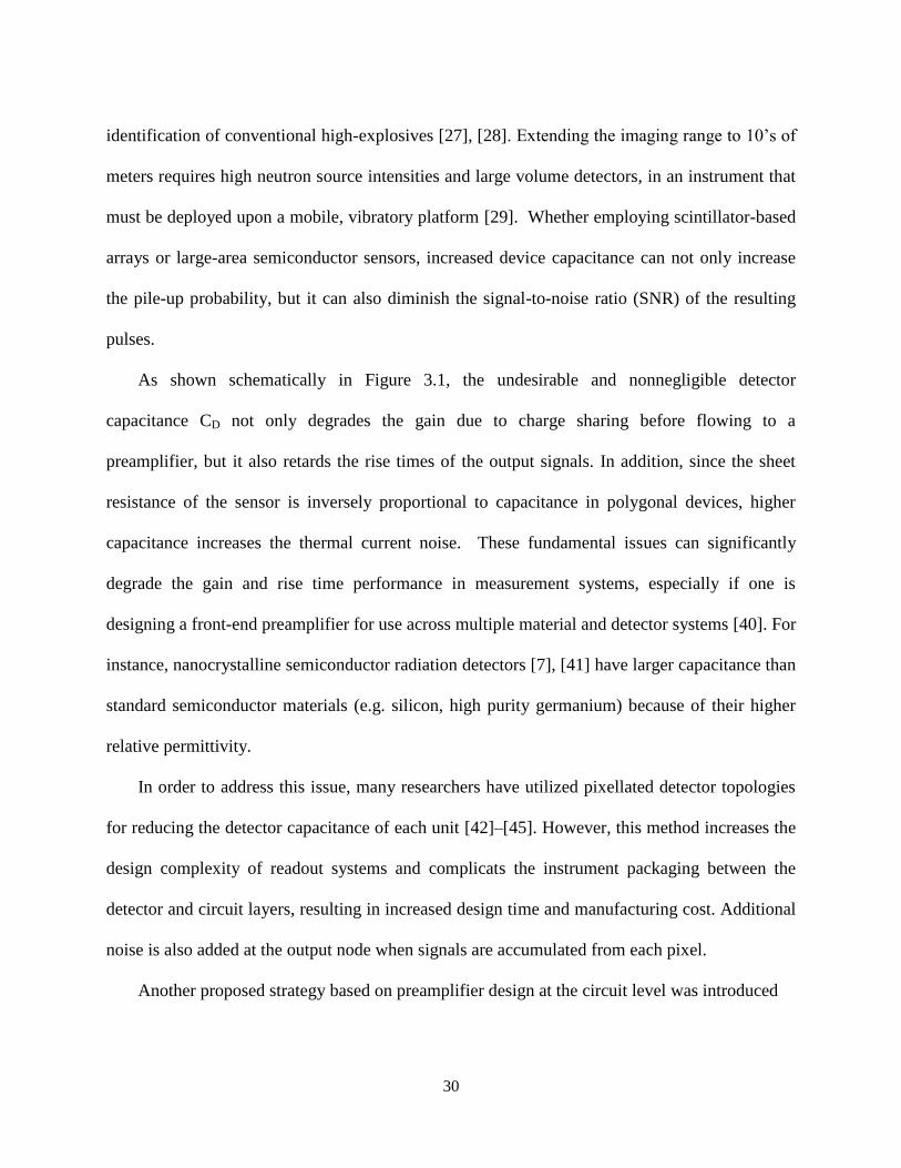
As shown schematically in Figure 3.1, the undesirable and nonnegligible detector
capacitance CD not only degrades the gain due to charge sharing before flowing to a
preamplifier, but it also retards the rise times of the output signals. In addition, since the sheet
resistance of the sensor is inversely proportional to capacitance in polygonal devices, higher
capacitance increases the thermal current noise. These fundamental issues can significantly
degrade the gain and rise time performance in measurement systems, especially if one is
designing a front-end preamplifier for use across multiple material and detector systems [40]. For
instance, nanocrystalline semiconductor radiation detectors [7], [41] have larger capacitance than
standard semiconductor materials (e.g. silicon, high purity germanium) because of their higher
relative permittivity.
In order to address this issue, many researchers have utilized pixellated detector topologies
for reducing the detector capacitance of each unit [42]–[45]. However, this method increases the
design complexity of readout systems and complicats the instrument packaging between the
detector and circuit layers, resulting in increased design time and manufacturing cost. Additional
noise is also added at the output node when signals are accumulated from each pixel.
Another proposed strategy based on preamplifier design at the circuit level was introduced

31
Vout
-
+
Op-amp
CF
CDIS
Radiation Detector
Detector Bias
Q
Figure 3.1: Traditional charge-sensitive amplifier with a radiation detector model. Charges
produced by the detector are shared between the detector and feedback capacitances, affecting
the gain of the front-end readout circuit.
to compensate for detector capacitance via transimpedance amplifiers (TIA) [46], [47]. Since the
technique maintains a voltage difference across a detector via an additional unity-gain amplifier,
a following preamplifier essentially sees no input capacitance from the detector. Nevertheless,
the strategy is not suitable for radiation detectors because a TIA exploiting the technique results
in a slow signal processing time (< MHz) due to the limited bandwidth of the unity-gain
amplifier, relative to standard high-speed TIA configurations. Unfortunately, the TIA gain is
also modified by the input voltage provided by the detector bias supply.
In this chapter, a detector capacitance compensation technique utilizing the Miller Effect is
detailed for use in those detector applications in which the sensor capacitance significantly
impacts the SNR and bandwidth of the readout. The preamplifier configuration exploits the
Miller Effect to transfer a voltage change from one side of a detector to the other side, thus
reducing the capacitance presented by the detector to the preamplifier. The entire circuit is
designed at the transistor level and implemented in a 180 nm standard CMOS technology for
portable, low power, and high-speed measurement applications. The preamplifier structure offers
32
the possibility of processing the induced charges generated by large radiation detectors to
charge-sensitive front-end circuits.
3.2 Integrated Circuit Design
As shown in Figure 3.1 and (3.1), the performance of the CSA is significantly influenced by
the detector capacitance, CD, if it is not small compared with the product of the feedback
capacitance, CF, and the gain of the operational amplifier, A:
. (3.1)
In (3.1), Q is the total charge generated within the detector. A higher intrinsic detector
capacitance also causes an increase in the total noise as well as degradation in the charge-to-
voltage gain at the output. The RMS thermal noise in terms of charges corresponding dark
current is simply defined as:
. (3.2)
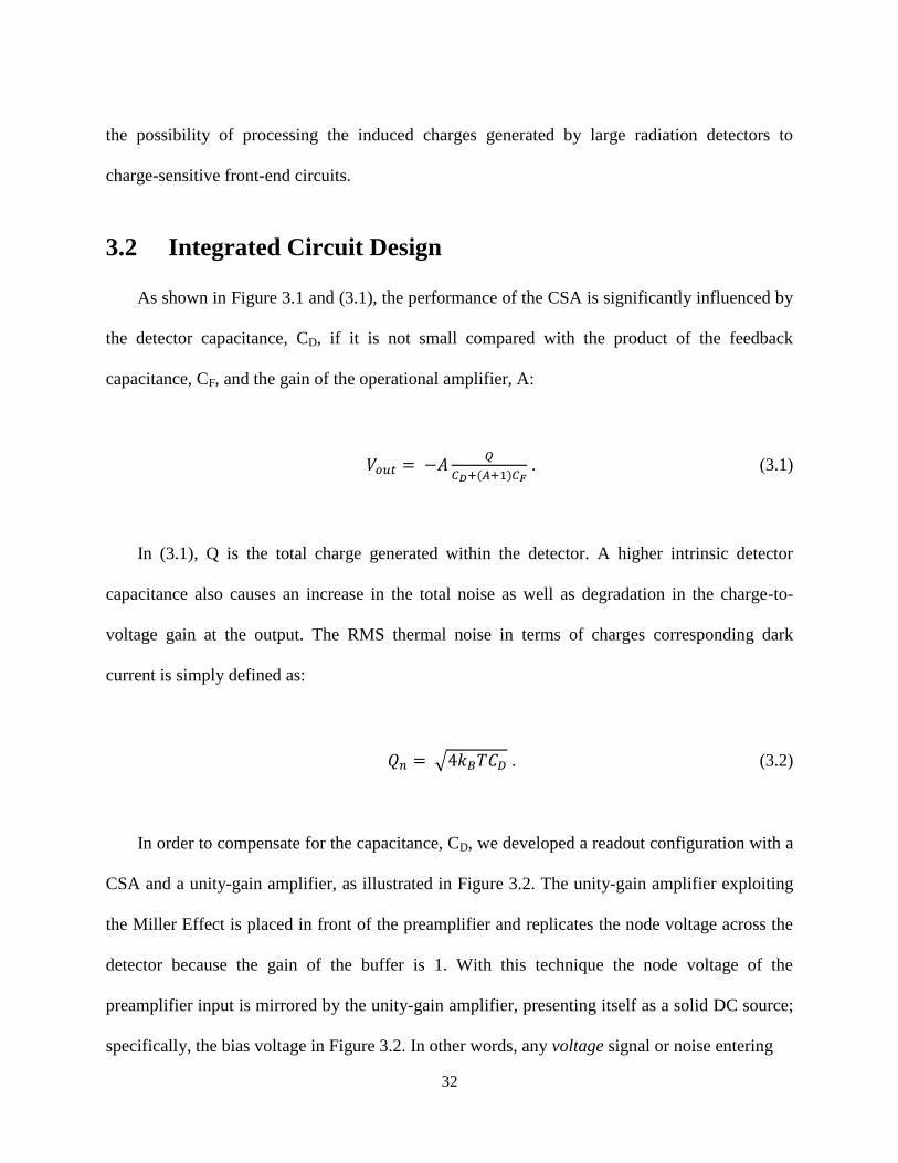
In order to compensate for the capacitance, CD, we developed a readout configuration with a
CSA and a unity-gain amplifier, as illustrated in Figure 3.2. The unity-gain amplifier exploiting
the Miller Effect is placed in front of the preamplifier and replicates the node voltage across the
detector because the gain of the buffer is 1. With this technique the node voltage of the
preamplifier input is mirrored by the unity-gain amplifier, presenting itself as a solid DC source;
specifically, the bias voltage in Figure 3.2. In other words, any voltage signal or noise entering

33
H. V.
CDIS
CSA
Radiation
Detector
Unity-gain
amplifierCC
CCG=1
RS
RS
Figure 3.2: Configuration with a charge-sensitive preamplifier and a unity-gain amplifier to
compensate the detector capacitance.
the preamplifier is directly transferred to the other side of the detector through the unity-gain
amplifier, while current signals converted from radiation impact events on the detector flow into
the preamplifier to experience gain in the normal manner. Note that the coupling capacitor CC
prevents the DC output voltage of the unity-gain amplifier from flowing into the bias node of the
detector, which may require very high bias voltage in order to establish a strong drift field.
For the practical integration with the detector, some passive components are needed to place
around the preamplifier chip and detector as shown in Figure 3.2. To block DC sources of
ground and high voltage bias for the detector, two coupling capacitors of 10 nF, CC, are used for
each input of the preamplifier. The series resistors, RS, should be big enough to prevent AC
signals passing to power sources such as ground and high voltage bias. Note that too large of a
resistance can also generate much more noise that degrades the resolution. Therefore, the proper
value of circuit resistors should be carefully chosen depending on the application targeted.

34
3.2.1 Miller Effect
The unity-gain technique is using a variation on the Miller Effect shown in Figure 3.3. The
equivalent input impedance Zin increases or decreases with the voltage gain of the amplifier,
which can be calculated as:
(3.3)
where Vi and ii are the input test voltage and current applied to the system. In our case, the
feedback factor Z is the intrinsic capacitance CD of a detector. By replacing Z with CD, the
equivalent input capacitance Cin is reformed as:
. (3.4)
With this technique, Cin can be ideally zero if the amplifier gain is equal to 1.
3.2.2 Design of Unity-Gain Amplifier
In order to design a unity gain amplifier, a common op-amp in which its output is connected
to its inverting input, was implemented as shown in Figure 3.4. The op-amp has two differential
inputs and a diode-connected load for the single-ended output, exhibiting a 3 dB bandwidth of
435 MHz and a unity gain of -0.14 dB which is equal to 0.984, as shown in Figure 3.5. Note that
the capacitor CA is inserted for a feed-forward compensation to prevent gain peaking near the
roll-off in the frequency response, which leads to a more stable gain and wider bandwidth [48].

35
Zin
Z
VoGain = A
Figure 3.3: Circuit diagram of the Miller Effect which is applied to the unity-gain amplifier in
order to seemingly have zero detector capacitance for the downstream readout circuits.
VoutVin
CA
Bias
Figure 3.4: Unity-gain amplifier design with a unity-gain operational amplifier.
The bandwidth of the unity-gain amplifier should be wider than that of a CSA so that its
effect is insensitive to voltage fluctuations in the range of preamplifier inputs. Otherwise, high
frequency components would pass the unity-gain amplifier into the preamplifier, resulting in the
failure of detector capacitance compensation. For this reason, we chose a single-stage design for

36
Figure 3.5: Voltage transfer function of the unity-gain amplifier.
enough bandwidth along a number of existing op-amp structures, which fully covers the CSA
bandwidth of 15.85 kHz as described in the next sub-section.
3.2.3 Design of Charge-Sensitive Amplifier
The core stage of the CSA in Figure 3.6 was designed with a conventional two-stage op-amp
architecture including a current mirror for constant current sources. One of two inputs, Vfeedback is
connected to Vout through an on-chip feedback capacitor of 1 pF and a resistor of 10 MΩ at the
top level design. Figure 3.7 shows the frequency response of the CSA indicating a voltage gain
of 140 dB and the 3 dB bandwidth of 15.85 kHz which is covered by the unity-gain amplifier
bandwidth as previously discussed. Finally, the stability is demonstrated in the closed- loop gain
and phase depicted in Figure 3.8, for which a safe phase margin of 84⁰ at the point of 0 dB gain
is achieved.

37
VfeedbackVin Vout
Ibias
Figure 3.6: Charge-sensitive amplifier design with a two-stage operational amplifier including a
current mirror.
Figure 3.7: Voltage transfer function of the charge-sensitive amplifier.

38
(a)
(b)
Phase margin of 84º
Figure 3.8: (a) Closed-loop gain and (b) phase transfer functions of the charge-sensitive amplifier
with feedback components. Phase margin of 84⁰ is shown.
3.3 Chip Implementation Details
The integrated circuit was implemented in a standard 0.18 μm standard CMOS technology,
and it was designed with thick oxide transistors that allow a relatively high supply voltage of 3.3
V. Figure 3.9 (a) is the die photo and (b) is the packaged chip in a DIP socket and mounted on a
PCB for convenient testing. The chip size is 512.84 μm x 464.84 μm including 15 pads of 60 μm
x 70 μm each for power and in/out pins. The total power consumption is 3.1 mW distributed

39
(a)
(b)
Figure 3.9: (a) Die photo and (b) wire-bonded chips on a printed circuit board for testing.

40
as follows: 2.5 mW for the unity-gain amplifier, 0.46 mW for the CSA, and 0.1 mW for the
current mirror based on parasitic-extracted layouts.
In order to measure the robustness of the design after fabrication, 10,000 Monte Carlo
simulations were performed to verify allowable uncertainties of gain and rise time at the system
outputs against process, voltage, and temperature variations. The histogram results are illustrated
in Figure 3.10 and tabulated in Table 3.1, exhibiting 1.68 % and 4.67 % fractional standard
deviations for the charge-to-voltage gain and rise time, respectively. The results indicate that the
chip will safely operate without system failure under manufacturing and environment
uncertainties.
3.4 Simulation Results
3.4.1 Transient Analysis of Charge-to-Voltage Gain and Rise Time
A radiation detector was modeled with a current source and a capacitor. We assumed, based
on measured radiation pulses in silicon semiconductor sensors, that the detector generates 11 fC
within 10 ns including 1 ns rise and fall times. The transient CSA outputs with different values of
detector capacitance from 1 pF to 1 nF in decade are shown in Figure 3.1 (b). At increased
detector capacitance, the amplitude of the output is dramatically decreased as discussed in
Chapter 3.2. The rise time of the pulses is also extended by increasing the detector capacitance,
which can increase the pulse pile-up probability.
Figure 3.12 (b) shows that the proposed detector compensation technique successfully
mitigates the effect of the detector’s inherent capacitance. The system bandwidth in Figure 3.12
(a) is maintained with higher detector capacitance while it is proportionally decayed in Figure
3.11 (a). Although the pulse outputs are not perfectly produced at a high capacitance of 1 nF,

41
Figure 3.10: Ten thousand Monte Carlo simulations of the charge-to-voltage gain (top) and rise
time (bottom) at the output indicate that the readout system is robust against process, voltage and
temperature variations.
Table 3.1: Charge-to-voltage gain and rise time with the technique at the best and worst
statistical model. One sigma standard deviations are also tabulated.
Charge-to-Voltage Gain (V/C)
Rise Time (ns)
16.4 G
4.86
σ (std) Best Worst
1,151 G
148.185.44
821 G

42
(a) (b)
Figure 3.11: (a) Frequency and (b) transient responses of the charge-sensitive amplifier without
the technique. Charge-to-voltage gain is dramatically reduced by detector capacitance increase
for a standard CSA.
(a) (b)
Figure 3.12: (a) Frequency and (b) transient responses of the charge-sensitive amplifier with the
technique. Charge-to-voltage gain is preserved even though detector capacitance increases.

43
Figure 3.13: Charge-to-voltage gain and rise time at the output of the charge-sensitive amplifier
are maintained as the detector capacitance increases.
which is a value for a 1 mm thick, 100 cm2
silicon detector, the preamplifier still delivers large
gain at high capacitance. Since the gain of the actual unity-gain amplifier does not typically
achieve the ideal value of 1, the improvements accrued from the Miller Effect are limited at
extremely large detector capacitance.
The relationship between the preamplifier and detector capacitance is presented in Figure
3.13. The charge-to-voltage gain and rise time (dotted lines) of the preamplifier without the
technique are both decreased in decade while they are sustained when the technique is utilized
(solid lines).
44
3.4.2 Noise Analysis
Because the detector capacitance compensation technique preserves the system bandwidth
as the detector capacitance increases, the accumulated output noise in the frequency domain is
increased in the broadband. Furthermore, the total output noise increases due to thermal noise
via the larger detector capacitance. Figure 3.14 (a) shows that the total RMS voltage noise of the
preamplifier increases at larger detector capacitance. In contrast, the output noise of the
traditional preamplifier is saturated because the system bandwidth is reduced by the detector
capacitance increase. Nevertheless, the signal-to-noise ratio (SNR) of the unity-gain preamplifier
is substantially enhanced because the detector capacitance - without the aid of the technique -
degrades the charge-to-voltage conversion. Consequently, the technique does not help to reduce
the fundamental noise physically generated in devices but it does boost the signal gain to
produce suitable outputs for downstream components, such as analog-to-digital converters
(ADCs), multi-channel-analyzers (MCAs) and microprocessors.
3.5 Radiation Detectors
In order to verify the feasibility of the technique to the practical application, radiation
detection, we measured two different sizes of silicon detectors, calculating different capacitances
based on their surface area. Figure 3.15 shows (a) a silicon radiation detector of 2 mm diameter
and (b) shows a 10 mm diameter device, resulting in calculated detector capacitances of 0.65 pF
and 16.25 pF, respectively.
3.5.1 Fabrication and Structure
We use various types of solid state radiation detectors such as Si, CdZnTe, CdTe, but we

45
(a) (b)
Figure 3.14: (a) Total output noise is increased with detector capacitance. Nevertheless, (b) the
SNR is much higher for the unity-gain amplifier than for the preamplifier without the technique.
(a) (b)
Figure 3.15: Two silicon radiation sensors (a) and (b) have different detector capacitance of 0.65
pF and 16.25 pF used for verifying the detector capacitance compensation technique.

46
selected Si detectors for this study due to its matured fabrication process to control the detector
parameters such as doping concentration and the junction depth that are critical factors for
lowering leakage current. Silicon radiation detectors are fabricated with high resistive (10 kΩ-
cm) 4" n-type phosphorus doped <100> wafer and the detectors have the PIN diode structure.
The first process step is the poly Si layer deposition on the bottom of the wafer as shown in
Figure 3.16 (b) and phosphorus is diffused into the poly Si layer and annealed. During the
thermal diffusion and the following annealing process, not only phosphorus is diffused but
impurities are also diffused toward the poly Si layer and they are trapped by grain boundaries of
the poly-Si. This gettering process allows the leakage current suppression by lowering the
concentration of the impurities in an active region of the device. An oxide layer also grows on
both top and bottom sides of the wafer as indicated in Figure 3.16 (c). The diode area is defined
with the photoresist (PR) patterning and the buffered HF etching for the selective oxide layer
etching. For the p+ doped region of the diode, boron is thermally diffused on the selectively
defined diode area and the remaining oxide layer functions as a mask for the boron diffusion.
The following step is to pattern the metallization area and deposit the metal with an e-beam
evaporator. After the lift-off process, the passivation layer is required for the prevention of the
deterioration of the device performance such as further oxidation. The passivation layer consists
of a 200 nm oxide layer and a 300 nm thick nitride layer. The bottom metal deposition is the last
fabrication process step. With this fabrication process, we were able to suppress the noise with
optimized surface passivation and the gettering process, the effectiveness of which is
demonstrated in [49], [50]. The low surface-leakage detectors are fabricated which then serve as
an effective platform to compare the effect of the detector capacitance compensation technique.

47
Figure 3.16: Schematic of the fabrication processes for the pin type Si detector.
3.5.2 Capacitance Comparison of the Sensor
The Si detectors are designed in two different geometric sizes in the form of 2 mm and 10
mm diameter circles. The capacitance from the parallel plate can be represented as (3.5) where ε0
is the vacuum permittivity, εr, is the relative permittivity of the silicon, r, is the radius of the
circular diode, and d is the gap between the two plates. According to the equation, the radius
difference is 5 times between the large and small diodes, which results in 25 times area
difference and a concomitant capacitance difference. If we assume the parallel same plate and
the junction gap as the entire wafer thickness, the 2 mm and 10 mm diameter diodes have 0.65
pF and 16.25 pF of capacitance, respectively.
Silicon wafer
N+
P+
N+
oxide
N+
Bottom Metal
N+
Passivation layerTop Metal
P+
N+
P+
(a) (b)
(c) (d)
(e) (f)

48
(3.5)
For the more accurate analytic approaches, however, the fringe capacitance has to be
considered because the bottom side area is much larger than the top. From the approximate
formula for the capacitance of a circular disc [51], the equation will have additional terms due to
the fringe capacitance as shown in (3.6). The fringe capacitance terms increase and the
proportional increase is more significant in smaller diode as illustrated in Figure 3.17.
(3.6)
In addition to the fringe capacitance, the junction gap is determined by the depletion region
thickness which depends on the bias voltage and the doping concentration. Capacitance-voltage
(C-V) testing, therefore, is widely used for the accurate measurement of the junction capacitance.
Measured capacitances in Figure 3.18 are larger than the analytically estimated values because
the diode has the smaller junction gap than the entire silicon wafer thickness. The capacitance
decreases as the reverse bias voltage increases, because the depletion region grows at higher
reverse bias voltages until it is fully depleted. We used the Keithley 4200 Semiconductor
Characterization System for the C-V measurement in which the compliance bias voltage is 30 V.
Capacitance values are measured at 10 V, 20 V, and 30 V reverse bias and the results are shown
in Table 3.2. Due to the limitation of the bias voltage, 30 V is the maximum value we measured.
Since the Si detector is operated at 100 V

49
Figure 3.17: Analytic capacitance comparison for the effect of the fringe capacitance.
Figure 3.18: Junction capacitance estimated from the formula (in the line) compared with the C-
V measured capacitance (in circles and triangles).
0 1 2 3 4 5 6 710
-1
100
101
102
Radius of the circular diode (mm)
Ca
pa
cita
nce
(p
F)
w/o fringe capacitance
w/ fringe capacitance
-100 -80 -60 -40 -20 010
-1
100
101
102
103
Reverse Bias Voltage (V)
Capacitance (
pF
)
2 mm diameter diode
10 mm diameter diode

50
Table 3.2: Capacitance of the 2 mm and 10 mm diameter circular diode from the C-V
measurement
Size(diameter) 10 V 20 V 30 V
2 mm 2.94 pF 2.54 pF 2.33 pF
10 mm 75.19 pF 39.54 pF 32.23 pF
reverse bias, we compared with the value from the junction capacitance formula, (3.7) [52]. Due
to the fringe capacitance, the 2 mm diameter diode has higher capacitance than the theoretical
value. The capacitance difference between the small and the big diode has to be 25 times, but the
C-V measured capacitance difference at 30 V shows approximately 14 times difference due to
the significant fringe capacitance in the 2 mm diameter diode as illustrated in Figure 3.18.
(3.7)
3.6 Measurement Results
3.6.1 Validation for Detector Capacitance Compensation
For observing the effect of detector capacitance on practical measurements we first
measured alpha particle spectra derived from 241
Am with only a conventional CSA in the chip.
As shown in Figure 3.19, the peak position of the large area detector was shifted significantly to
the left due to its capacitance (gain decrease). Note that all other environments and conditions
such as detector bias voltage, gain of the shaping amplifier, and distance of the radiation source
except the sensors are preserved for these measurements.

51
Figure 3.19: Alpha particle spectra of 241
Am measured by small (2 mm diameter) and large (10
mm diameter) area silicon detectors.
Next, we measured spectra of the same source with the small area detector by enabling the
detector capacitance compensation amplifier in Figure 3.20. With the technique, the peak is
slightly shifted up because of the compensated detector capacitance. However, the resolution is
not notably improved because the detector capacitance is already small enough and does not
significantly affect the original specifications of the CSA. In order to distinctly see the effect of
the compensation, we moved on the other detector which has 10 - 25 times bigger capacitance.
The measurement results with the large area detector as illustrated in Figure 3.21 shows
improvement on the gain and resolution. As can be seen, the peak location of the compensated
detector capacitance is channel number 4711 which is 1.75 times larger gain than that without
the technique. The resolution is also improved by 3.75%.
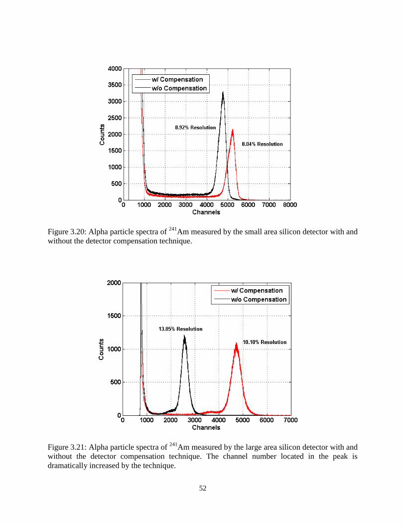
52
Figure 3.20: Alpha particle spectra of 241
Am measured by the small area silicon detector with and
without the detector compensation technique.
Figure 3.21: Alpha particle spectra of 241
Am measured by the large area silicon detector with and
without the detector compensation technique. The channel number located in the peak is
dramatically increased by the technique.

53
3.6.2 Analysis on Resolution and Energy Loss in Air
Since charged particles lose their energy throughout their path length, the measured
resolution can be varied if the range of the particle is altered. For the analysis we designed three
stands with different heights, 3.3, 2.5, and 2.2 cm to modify the energy of the alpha particle
incident upon the semiconducting volume. According to the reference [53] in Figure 3.22 each
distance in air between radiation source and detector corresponds to reduced energies, 1.15, 2.6,
and 3.05 MeV, respectively. As can be seen in Figure 3.23, the designed stands are placed in an
aluminum test box with the radiation detector to reduce any electromagnetic interference. The
box is completely enclosed while testing.
The Figure 3.24 results show that the degradation in the gain due to detector capacitance is
successfully compensated by the technique for high energy particle impact events. The red lines
are the peaks derived from 3.05 MeV alpha particles. Resolution and FWHM are improved to
10.10 % and 481 keV with the technique from 12.68% and 620 keV without the technique,
respectively. In addition, the channel number of the peak is dramatically increased by the
technique, promising the possibility on producing readable output signals even at larger detector
capacitance. For the lower energy particles at longer distances, the energy resolutions, however,
are worsened. This interesting phenomenon is neither wrong data nor chip malfunction, but is
rather a reflection of the relationship between noise and resolution, as follows.
The technique is implemented by a unity-gain amplifier which compensates the system
bandwidth, preserving the overall gain of the CSA. However, the additional component increases
the circuit noise relative to the CSA without the amplifier, resulting in worse resolution for lower
energy particles. Since the energy resolution is proportional to the accumulated circuit and
detector noise, the numbers inevitably get higher with the compensation amplifier. Nevertheless,

54
Figure 3.22: Comparison between experimental data (three sets) for alpha energies from 241
Am
in air as well as the calculations from ICRU data (dashed line), SRIM data (solid line) and SRIM
data x 0.95 (dotted line) [53].
Figure 3.23: Three stands producing 3.3, 2.5, and 2.2 cm gaps placed in a testing box for
analyzing the alpha energy loss in air.
inverse functions of the resolution related to gained signals and total noise are formed with
different constant values for the CSAs with and without the technique. From the different
resolution equations derived by the measured data, we came up with a crossover point

55
(a)
(b)
Figure 3.24: Alpha particle spectra of 241
Am measured by the large area silicon detector (a)
without and (b) with, the detector compensation technique. The spectra were measured on three
stands to observe different ion energies.

56
Figure 3.25: Reduced energy particles vs. resolution. The resolution gets better beyond 2.15
MeV particles by applying the detector capacitance compensation technique.
at 2.15 MeV with a 14.55% resolution as shown in Figure 3.25, beyond which particles can be
detected with better resolution by enabling the technique. Even though the resolutions of lower
energy particles get worse, those peaks are located in higher channel numbers as shown in Figure
3.24. This increased radiation-signal relative to the electronic-noise leads to better detection
ability because the spectra of larger radiation detectors will be moved to the left in channels due
to the decreased gain and buried into the noise if the technique is not applied.

57
CHAPTER 4
Razor-Lite: A Light-Weight Register for EDAC
4.1 Motivation
4.1.1 View of Radiation-Hardened-by-Design
For designing radiation hardened circuits applied to electronic devices in various space,
nuclear, and scientific applications, single event transients (SETs) and single event upsets
(SEUs) are of primary concern because they are the main phenomena that cause malfunctions in
a system by contaminating the data transition and flipping stored bits.
As illustrated in Figure 4.1, the effect of SETs is the production of data with a range of
amplitudes and time durations in a logic stage between registers composed of flip-flops. In
general, digital signals are processed in a logic stage between registers during one clock cycle,
which then propagates to the next stage duration the clock transition. The flip-flop as a register is
commonly used in digital circuits that require stability and high speed. Briefly summarizing the
conventional D Flip-Flop (DFF) of Figure 4.1, when the clock is low, the master latch is ready to
store data from the previous stage (red circle not activated) while the slave latch holds the data
for the next stage in the feedback system (blue circle). At the rising edge of the clock, the input

58
LogicStage
clk
SET
Reg. Reg.
Data
CLK
CLK CLK
D
CLK
CLK
CLKCLK
CLK
Q
Master Latch Slave Latch
Figure 4.1: A logic stage and registers in a clock based digital circuit (left). Traditional D Flip-
Flop schematic diagram (right).
data from the previous stage is “locked” and stored in the red circle during the high clock period.
By this mechanism in a digital circuit, data in both “transition” and “storage” phases are exposed
to radiation impact.
For many years, radiation-hardened-by-design (RHBD) circuits have been developed and
adapted from traditional circuit architectures. One common method is to utilize redundancy in an
important block to preserve the correct data. This technique performs a voting process to
produce a correct output when any one of the duplicated systems fails due to a SEE. For
example, B. Olson applied the redundancy technique, formally termed the triple modular
redundancy (TMR) [54]. In addition, a dual-path hardening technique implemented on a
multiplying digital-to-analog converter circuit (MDAC) and a comparator circuit results in
significant radiation hardening. Other methods use various error detection and correction
(EDAC) algorithms adding redundant bits in the storage components to detect and correct errors
at the system level [55]. These methods have been successfully adapted to applications requiring
radiation hardening; however, all of the techniques lead to performance penalties in speed, area
and resolution by adding TMR, voting circuits, and extra bits for EDAC methods. TMR requires

59
a three times expansion in area for redundancy circuits and EDAC needs more calculation time
as well as redundancy bit-storage units.
The multiplication of circuits in a rad-hard component increases the occupied area in an
integrated circuit in the form of transistors, capacitors, and resistors, the parasitic capacitance and
resistance from which reduces the overall performance of the system [56]. This performance
penalty is particularly unwelcome for radiation tolerant applications because they generally
demand high performance designs in terms of speed, resolution, and power. Even though high
performance can be increasingly delivered by the process development in sub-micron
technology, errors induced by radiation impacts increase in effect for smaller component size
because smaller charges used in the state-of-art integrated chip technology are more vulnerable
to induced charges generated by radiation-impact events.
In order to reduce this hardware and software burden, an in situ error detection flip-flop was
developed for multi-stage pipelined digital processors. This technique allows a system to
recognize a delayed signal as an error due to SET and recovery the error by a roll-back system by
recalculating the failed clock period.
4.1.2 View of Variation Tolerant Processor
In advanced technology nodes, process variation, voltage variation, temperature variation,
and aging effects (PVTA) cause significant performance uncertainty. In order to ensure correct
functionality, appropriate timing margins are added during design time. Consequently, these
margins result in losses in performance, energy, area, and cost: performance through reduction in
clock period, energy from increased supply voltage, area from increased design sizing, and cost

60
through increased tester time to measure these variations. Naturally, these losses form a trade-off
in which the designer must estimate how much of each loss is present in their design.
To address this issue, researchers have proposed strategies for measuring or estimating
timing margins using on-chip structures, which allow more certainty in variation measurement
with a smaller increase in tester time. A common approach uses “canary” replicated critical paths
and structures to accurately measure their delay [57]–[63]; this enables measurement and
mitigation of global and slow PVTA variations, but not local or fast variations. Additional
margins must be included for these techniques in order to compensate for the uncertainty in the
canary itself.
Another proposed strategy was introduced to predict failures caused by aging via early
failure detection circuits [64]–[66]. In order to more directly measure delay degradation (in
comparison to canaries), these circuits checked for data transitions of the inputs of flip-flops just
before the clock period in order to warn of future failures. However, the early error detection
technique cannot recover from timing failures and require applications with highly regular data
delays, e.g., in communication buses. Significant data-dependent delay variation can cause this
style of circuit to under-estimate aging degradation.
To further reduce PVTA margins, researchers have proposed in situ error detection and
correction (EDAC) circuits. These circuits operate by monitoring the system for timing
violations and then act to recover functionality of the design if such a violation occurs. This
strategy eliminates global, local, fast, and slow timing margins and includes only a small margin
for the uncertainty in timing violation detection. Examples of published EDAC techniques
include Razor I [67]–[69], Razor II [70], Transition Detector with Time Borrowing (TDTB) [71],
Double Sampling with Time Borrowing (DSTB) [71], [72], and Bubble Razor [73]. Together

61
these approaches have demonstrated 22 – 60 % energy savings in worst-case timing margins,
depending on the system architecture and process technology.
To implement an EDAC system, critical paths must be monitored using specialized registers
that can incur significant overheads, which increase depending on the number of monitored
paths. In previous Razor-type designs, 9 - 17% of the total register count is monitored as critical
paths for EDAC techniques [67]–[71], but modern commercial processors have well balanced
pipelines and require much greater insertion rates. The ARM Cortex-M3 would require 55 % of
registers to be monitored in order to detect late arriving data transitions in the last 20 % of the
clock period [73], [74]. The energy and resource efficiency for this case are visualized in Figure
4.2, where even moderate EDAC circuit insertion results in 30.5 % area and 9.2 % power system
overheads using the previously reported EDAC register [68]. In systems with a high insertion
rate, the overhead of the specialized registers detracts from the benefits of implementing an
EDAC system.
Past EDAC registers suffered from relatively high area and power overhead due to the
inherent complexity of detecting a data transition within a fixed window of time. Razor-I [68]
accomplished this with a shadow latch technique that used 44 additional transistors and required
clock and data-path loading. Razor-II [70] was able to eliminate the shadow latch and instead
used a gated transition detector, a technique that used 31 additional transistors and also
significantly loaded the clock and datapath. DSTB [71], which is a similar topology to Razor-I,
has extra clock and data-path loading by using shadow FFs. Unfortunately, these previous works
all incur additional clock loading and a substantial increase in transistor count over a traditional
design. Thus, in modern processors with well-balanced timing paths there is a need for
lightweight EDAC registers to minimize area and energy overheads.

62
0.0 0.2 0.4 0.6 0.8 1.0
0.0
0.1
0.2
0.3
0.4
0.5
0.6
0.7
0.8
0.9
1.0
20% of Clock Period
Fra
cti
on
of
Re
gis
ters
Monitored Delay Slack (Norm. to Tcycle)
55% of Registers
0.0 0.1 0.2 0.3 0.4 0.5 0.6 0.7 0.8 0.9 1.00
100
200
300
400
500
600
700
R
eg
iste
r C
ou
nt
Fraction of Clock Period
(a) (b)
Figure 4.2: (a) Clock period histogram and (b) fraction of registers by delay slack for an ARM
Cortex-M3 processor [73], [74].
In this chapter we describe Razor-Lite, which uses the inner nodes of a tri-state inverter
standard D flip-flop (DFF) as a side-channel late-signal detection mechanism. This detection
strategy requires only 8 additional transistors to generate an error flag without extra clock and
data-path loading. To illustrate the advantages of a compact EDAC register, a canonical low-
power microprocessor that replaces 20% of registers with the proposed Razor-Lite registers
shows 7.5 % and 1.4 % area and power overhead, respectively, compared to 30.5 % and 9.2 %
using a prior EDAC register [68] (Figure 4.3). The compact Razor-Lite register was
implemented in a 7-stage, 64-bit Alpha processor to verify functionality and reliability with a
simple roll back error recovery mechanism. This work focuses on the EDAC register design; a
number of existing methods have been published for architectural replay.

63
12.4 mW (+1.4%)13.4 mW (+9.2%)12.2 mW
155,000 m2 (+30.5%)119,000 m
2
Combinational
67.6%
Register
32.4%
Baseline
Pow
er
Com
pari
son
Are
a C
om
pari
son
Razor-LiteRazor [1]
Razor
23.4%
Combinational
51.8%
Register
24.8%
128,000 m2 (+7.5%)
Razor
7.0%
Combinational
62.9%
Register
30.1%
Combinational
17.5%
Register
51.6%
Clock Network
30.9%
Razor
8.4%
Combinational
16.0%
Register
47.3%
Clock Network
28.3%
Razor
1.4%
Combinational
17.2%
Register
50.9%
Clock Network
30.5%
(a) (b) (c)
Razor [9]
Figure 4.3: Overhead ratio comparisons of three ARM Cortex-M3 variants; a) baseline, without
EDAC, b) with 20% insertion of EDAC registers from [68], c) with 20% insertion of Razor-Lite
registers.
4.2 Design Overview
4.2.1 Razor-Lite Core Circuit
The Razor-Lite flip-flop supplements a standard design with light-weight detection circuitry
that does not perturb the critical path. The key observation that enables Razor-Lite is that the
desired error signals already exist in many commercial flip-flop designs; to access these signals
we need only to add appropriate buffering.
The input buffer to a DFF is usually either a tri-state inverter or the practically equivalent
inverter followed by a transmission gate. Razor-Lite uses a tri-state inverter so that the two

64
floating nodes (VVDD and VVSS) inside buffer are available, however if a DFF uses an inverter
followed by transmission gate, it can be quickly converted by removing one wire. The two
signals to be accessed are the floating nodes in the tri-state inverter (Figure 4.4). Monitoring
these inner nodes will enable timing error detection while avoiding additional clock and datapath
loading since these nodes will charge/discharge in the event of a timing violation, and operate
normally otherwise, as illustrated in Figure 4.5. The standard cell chosen from the commercial
library employs two additional inverter stages along the datapath for improved drive strength,
though this strategy can be applied to other standard cell implementations with an input latch that
is opaque for the positive clock phase - the later transistors do not change the fundamental
Razor-Lite technique.
Figure 4.5 shows timing diagrams of the Razor-Lite error detection based on clock and data
signal transition. Note that a low duty cycle clock is used here since the high phase of the clock
is equivalent to the speculation window, which in EDAC systems is defined as the time during
which errors are detected and correctable. Having an unnecessarily long speculation window is
undesirable due to the need for fast-path buffering (see Chapter 4.2.2 below).
The Razor-Lite register operates identically to a normal DFF when no timing violation
occurs since the monitoring circuitry does not impede the operation of the register. While the
clock is low, the virtual rails being monitored (VVDD and VVSS) are driven by supply or
ground independent of any input signal (D) transitions, and DN is driven to be the opposite of D.
After the clock rises, one of the virtual rails starts floating since M1 and M4 in Figure 4.4 are
turned off, however either VVDD or VVSS remains connected to DN depending on the state of
D. As long as D remains in the same state as when the master stage closed, DN remains equal to
the connected virtual rail. If D changes while in this state, the opposite virtual rail suddenly
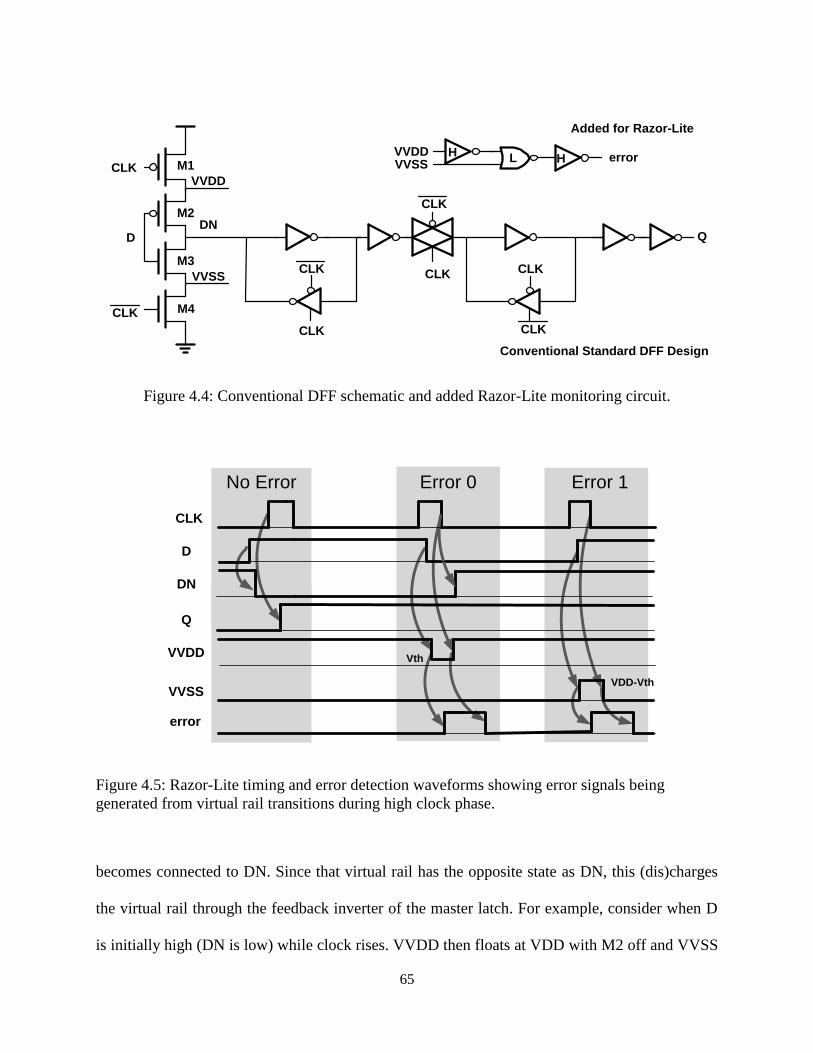
65
D
CLK
CLK
CLK
CLK
DN
VVDD
VVSS
CLK
CLK CLK
CLK
Q
HVVDDVVSS
HL error
Added for Razor-Lite
Conventional Standard DFF Design
M1
M2
M3
M4
Figure 4.4: Conventional DFF schematic and added Razor-Lite monitoring circuit.
Error 1
Vth
No Error Error 0
CLK
D
DN
Q
VVDD
VVSS
error
VDD-Vth
Figure 4.5: Razor-Lite timing and error detection waveforms showing error signals being
generated from virtual rail transitions during high clock phase.
becomes connected to DN. Since that virtual rail has the opposite state as DN, this (dis)charges
the virtual rail through the feedback inverter of the master latch. For example, consider when D
is initially high (DN is low) while clock rises. VVDD then floats at VDD with M2 off and VVSS
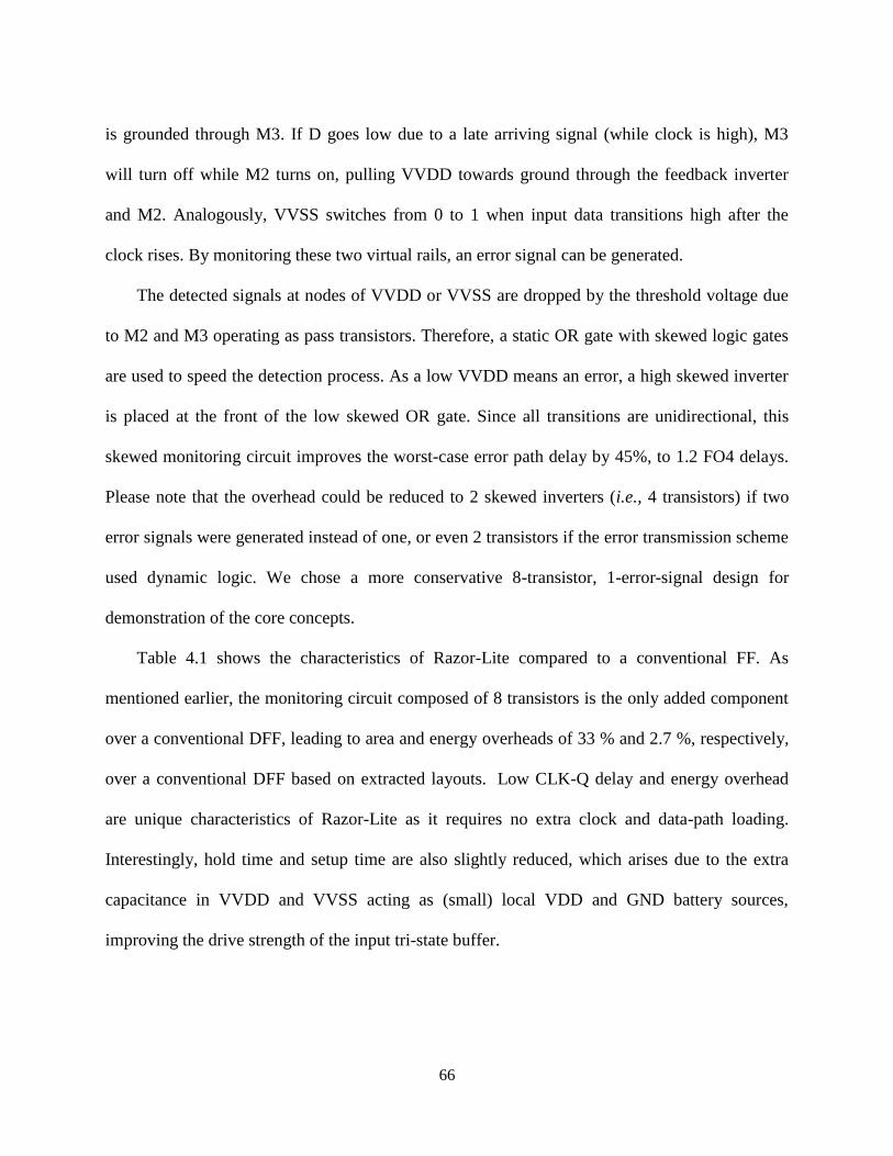
66
is grounded through M3. If D goes low due to a late arriving signal (while clock is high), M3
will turn off while M2 turns on, pulling VVDD towards ground through the feedback inverter
and M2. Analogously, VVSS switches from 0 to 1 when input data transitions high after the
clock rises. By monitoring these two virtual rails, an error signal can be generated.
The detected signals at nodes of VVDD or VVSS are dropped by the threshold voltage due
to M2 and M3 operating as pass transistors. Therefore, a static OR gate with skewed logic gates
are used to speed the detection process. As a low VVDD means an error, a high skewed inverter
is placed at the front of the low skewed OR gate. Since all transitions are unidirectional, this
skewed monitoring circuit improves the worst-case error path delay by 45%, to 1.2 FO4 delays.
Please note that the overhead could be reduced to 2 skewed inverters (i.e., 4 transistors) if two
error signals were generated instead of one, or even 2 transistors if the error transmission scheme
used dynamic logic. We chose a more conservative 8-transistor, 1-error-signal design for
demonstration of the core concepts.
Table 4.1 shows the characteristics of Razor-Lite compared to a conventional FF. As
mentioned earlier, the monitoring circuit composed of 8 transistors is the only added component
over a conventional DFF, leading to area and energy overheads of 33 % and 2.7 %, respectively,
over a conventional DFF based on extracted layouts. Low CLK-Q delay and energy overhead
are unique characteristics of Razor-Lite as it requires no extra clock and data-path loading.
Interestingly, hold time and setup time are also slightly reduced, which arises due to the extra
capacitance in VVDD and VVSS acting as (small) local VDD and GND battery sources,
improving the drive strength of the input tri-state buffer.

67
Table 4.1: Razor-Lite register delay, energy, and area overhead compared to a traditional DFF, as
determined by SPICE simulation including layout parasitics.
Area 6.7µm 1.33×
Error Event N/A1.55× DFF
energy
Hold Time -5.48ps 0.72×
Setup Time 10.30ps 0.95×
CLK-Q Delay 54.34ps 1.004×
Switching Energy 15.8fJ 1.02×
Leakage Energy 5.69fJ 1.04×
Razor-Lite
(Norm)
Conventional
FF
2
4.2.2 Duty-Cycle Controller
The speculation window is controllable in most EDAC-type systems [69, p. 32], [70]–[73].
In this work we pay particular attention to optimizing the speculation window and demonstrate
an algorithm that achieves good timing margin coverage while minimizing fast path false
errors. The fundamental tradeoff here stems from the need to distinguish late-arriving data of
cycle n from early-arriving data of cycle n+1. In addition, we seek a large speculation window
to capture timing errors and allow for aggressive voltage scaling, exacerbating the issue as even
more fast paths could be flagged as late-arriving data from the prior cycle. With this clock
generation scheme it is important to constrain the skew of both the rising and falling edges of the
clock. Since the pulse is around 12 FO4 delays wide, it is not as challenging to distribute as in

68
pulsed latch systems, which have pulses ~ 2 FO4 delays wide. The larger hold time constraint
leads to more buffering and associated energy costs; these are offset by the voltage scaling
enabled by the EDAC elements.
The typical error detection scheme illustrated in Figure 4.6 depicts how margins are
included in a typical “always correct” scenario as well as the “detect and correct” scenario. The
worst-case margins assumed in the “always correct” scenario are on average significantly worse
than the actual PVT variations. In the “detect and correct” scheme these variations are measured
and the corresponding energy and performance impacts are reduced. While the margins
associated with many variations are eliminated, the speculation window must account for fast
variations that cause late arriving signals, which can be defined as:
(4.1)
where TW is the speculation window and Tc_path is the critical path delay including uncertainty
due to temperature, local, and global variations.
The hold time constraint for preventing false errors is calculated as:
(4.2)
where Ts_path is the shortest path delay (including uncertainties) and Tclk-q is the propagation
delay from the rising clock to the flip-flop output. Even though Razor-Lite allows the shrinking
of margins before the rising clock edge because of its EDAC nature, we must adhere to these
constraints to maintain overall chip functionality.

69
Uncertainties “Before” (Always Correct)
Data JitterTempGlobal
ProcessVolt
CLK
Actual Circuit Delay Required Margins
Fast Variations
SkewLocal
Process
Uncertainties “After” (Detect & Correct)
CLK
Actual Delays
CLK
D
TW
Tcycle
Tc_path Tsetup
Thold
Ts_path
Logic Stage Logic StageDFF DFF
Data JitterTempGlobal
ProcessVolt Skew
Local
Process
Tw
Figure 4.6: Conceptual timing diagram for required speculation window to manage hold time
constraint issue and late arrival signal detection in the Razor scheme by detecting and correcting
errors.
In order to balance the dual requirements of maximizing speculation window while
minimizing the hold time constraint, we implemented a duty cycle controller to tune the
speculation window, further allowing Razor-Lite to compensate for PVTA variations. This
strategy is implemented with a tunable pulse generator (Figure 4.7 (a)) to control clock duty,

70
HALF_CLK
...M
UX
Digital_CTRL
HALF_CLK
D D D
D D
...
CORE_CLK
...
Duty Cycle Controller Duty cycle
Measurement Unit
Free-Running
Ring Oscillator
CORE_CLK
DUTY
CYCLE
D Q
Clk
D Q
Clk
D Q
Clk
COUNTER
COUNT
DOWN
UP EN
(a) (b)
Figure 4.7: (a) Schematic of the tunable pulse generator used for duty cycle control; (b) statistical
sampling circuit for measuring duty cycle.
similar to [71]. Figure 4.7 (b) shows the duty cycle measurement unit, which is implemented as
a statistical sampling circuit. This circuit uses a free-running ring-oscillator to sample the system
clock at the counter; two additional DFFs are included to avoid metastability.
We apply the dynamic duty cycle control algorithm of Figure 4.8 to optimize the speculation
window. For initial duty cycle calibration, the processor first runs with 50 % duty cycle at a half
frequency so that only fast path errors will be detected. After each run, the measured error rate is
compared to our previously set target. If the error rate exceeds the target, duty cycle is reduced.
This initial algorithm sets the fast path error rate below a reasonable target. During run-time
calibration, processor replay at half the nominal clock frequency is performed upon error
detection. If an error is detected again in the following reply, we can safely conclude that both
errors are caused by a fast path violation. In this case the duty cycle is reduced to suppress these
fast path errors. Otherwise, the initial error is defined as a slow path violation (i.e., late arriving
signals). If slow path violations consistently occur during runtime calibration

71
Initial Calibration
Run Processor @ ½
CLK Frequency
Reduce Duty Cycle
Error Rate > Target ?
STOP
YES
NO
Set Duty Cycle=50%
Run-time Calibration
Processor gets
an error
Error Again?
Re-Run @ ½
CLK Frequency
Reduce Duty
Cycle
YES
Back to Normal
Operation
i=i+1
(initialized to 0)
NO
i > i_MAX ?
NO
Increase Duty
Cycle(i=0)
YES
Slow path
violation
Fast path
violation
Figure 4.8: Calibration sequences to dynamically tune duty cycle for maximum speculation
window while avoiding the flagging of errors due to fast paths.
such that they exceed a threshold (user-defined), the duty cycle is dynamically increased to
maximize speculation window and effectively capture the widest possible set of timing errors.
The measured error count rates in Figure 4.9 confirm that the proposed control algorithm
improves the practicality and performance of a duty cycle control system by balancing the two-
sided constraint between hold time and speculation window.

72
110 115 120 125 130 135 140 145
0
10k
20k
30k
40k
50k
Err
or
Co
un
t
Duty Cycle (ps)
Figure 4.9: Measurement results show that tuning duty cycle has a large impact on error rates
and overall system performance/efficiency.
4.2.3 Metastability Considerations
Similar to previous flip-flop based EDAC work [67], [71], Razor-Lite introduces the
possibility of metastability in the datapath [75]–[77]. In the first tri-state buffer of Figure 4.4, DN
can fall into an unstable equilibrium (“metastable level”) between VDD and GND if a data
transition occurs near the rising clock edge. This is an important issue in EDAC systems since
the long metastability resolution time point can lead to failure in detecting timing errors (i.e., a
decision cannot be made during the speculation window). Razor-Lite inherently resolves this
issue by predictably limiting the duration of metastability.

73
Figure 4.10 depicts the four different cases of Razor-Lite transient behavior as it relates to
metastability. In Cases 1 and 2, long metastable states of DN trigger the detection signal since
virtual rails are charged up or down as errors even though the state settles correctly later. Short
metastable events are resolved within the detection window and result in either an increased
CLK-Q delay in Case 3 or the re-running of the instruction with an error flag (by rollback
mechanism) in Case 4. Case 3 is the only problematic scenario as the data transition to the next
pipeline stage can be delayed. However, the maximum added delay is 2.67 FO4 delays in worst-
case conditions (0.9V, 85C, SS corner), which can be absorbed by EDAC sequences in the next
stage.
Monte Carlo DC simulations were performed to verify the error detection ability for long-
term metastability of Case 1 and 2. Due to the skewed switching thresholds of the detection
circuit, any metastable voltage levels should lie within the detected voltage range. Figure 4.11
shows results of 106 Monte Carlo simulations at 5 corners; the lowest margin observed is
100mV, confirming that long-term metastability will be detected by Razor-Lite as an error and
the instruction re-executed.

74
DN
Detect
CLK
D
Q
CASE 1
Critical Metastability
Detection
DN
Detect
CLK
D
Q
CASE 2
Critical Metastability
Detection
DN
Detect
CLK
D
Q
CASE 4
Non-Critical Metastability, DN resolves to wrong state
Detection
Resolves to wrong state
DN
Detect
CLK
D
Q
CASE 3
Non-Critical Metastability, DN resolves to correct state
No Detection
Resolves to correct state
CLK-Q Penalty 2.67 FO4 delays
WC(0.9V,85C,SS)
Metastable Metastable
Metastable Metastable
Figure 4.10: Timing diagrams showing the transient behavior of Razor-Lite in response to both
long-term (Cases 1 and 2) and short-term (Cases 3 and 4) metastable events at DN.
Minimum
Margin
Minimum
Margin
Figure 4.11: One million Monte Carlo DC simulations of the voltage difference between
monitoring circuit switching threshold (VT, for each VVSS at left and VVDD at right) and
metastable voltage level of node DN. Results indicate that substantial margin exists to avoid
metastability.

75
4.2.4 Virtual Rail Leakage
Previous related work [69] – [71] that heavily relied on dynamic operation also reported
design complexity due to process variation sensitivity. In contrast, Razor-Lite has a static
detection path since the charging or discharging of virtual rails comes from the feedback of the
master latch, thereby offering robustness against process variation. However, leakage-induced
false positive errors should be carefully considered since one of the virtual rails is floating during
the high clock phase. To illustrate, when the data input to the Razor-Lite FF is low, VVDD is
static by the feedback inverter through M2 in Figure 4.4 while VVSS floats. Fortunately, the
virtual rails cannot easily leak away from their nominal values; in this specific case there is
negative Vgs on M3, greatly reducing leakage while the leakage on clocked transistor M4 also
resists charging of VVSS.
To confirm immunity to this potential leakage issue, both simulation and measurement-
based verification was performed. In 105 Monte Carlo simulations, no leakage-induced false
errors were observed for practical (≥1 MHz) clock rates. In addition, in hardware (chip
implementation details provided in Chapter 4.3 below) the free running processor (running no-
op’s) at 85°C, SS corner, and the minimum clock frequency of 20.16 MHz showed no additional
errors induced by the leakage issue (i.e., the number of errors was not a function of speculation
window). A long speculation window was used in this experiment through increased duty cycle.
4.2.5 Low Voltage Operation
Razor-Lite is designed to detect late transitions while remaining as light weight as possible.
Part of this detection scheme uses intermediate voltages since an NMOS transistor is passing a 1
and a PMOS transistor is passing a 0. Because of this, Razor-Lite as described has limited

76
voltage scalability; it operates down to 750 mV supply voltage as verified by 10k Monte-Carlo
simulations. More aggressive near-threshold operation can be achieved by augmenting the
current design with four additional transistors. As shown in Figure 4.4, the two pass transistors
are M2 and M3, which are enabled by the data input ‘D’. If D-complement is generated using an
inverter, then M2 and M3 can be supplemented to become full transmission gates, eliminating
the intermediate voltages in the circuit. These additional transistors do not add clock loading or
clock energy, but incur a slight setup-time penalty (12 %) and data-switching energy increase (10
%). For the modified TG-based design, operation is verified down to 400mV supply via Monte-
Carlo simulations, which is well below the nominal voltage of 1.1V and the iso-performance
operating voltage of our fastest chip, which is 850mV as will be shown in Chapter 4.4.
4.3 Chip Implementation Details
Razor-Lite is implemented in a 7-stage, 64-bit Alpha architecture pipeline, as illustrated in
Figure 4.12. The decode and execute stages were the most critical stages based on timing slack
analysis of all paths with extracted layout components, and hence all 492 decode and execute
stage registers use the Razor-Lite register. Errors are aggregated using an edge-triggered OR tree
and passed through stabilization registers to mitigate metastability in the error path.
This aggregated, stabilized error passes to the FSM error controller, which generates a signal for
the half clock generator and the core to trigger a replay mechanism for error correction. Figure
4.13 shows the waveform of a single error triggering system replay. Once an error is detected,
the pipeline operates with a 50 % clock frequency for 4 cycles to re-execute correctly the
problematic instruction, with a total penalty of 11 cycles. The Razor-Lite FF can be used in other
EDAC architectures as well since the register design is orthogonal to correction scheme.

77
IF S
tage
Sta
ndard
FF
IF2 S
tage
Sta
ndard
FF
ID S
tage
Razo
r-Lite F
F
EX S
tage
Razo
r-Lite F
F
MEM
Sta
ge (
Read-O
nly
)
Sta
ndard
FF
WB
Sta
ndard
FF
WB2(r
eg/D
MEM
)
Duty Cycle Controller Half Clock Generator
Edge Triggered Or Tree
FSM
Error Controller
...
...
...
ERROR
D Qgroup
error
stabilized errorSLOW
FLUSHCORE
CLK
ALPHA 64 Architecture Processor
Figure 4.12: System block diagram of Razor-Lite implemented in an Alpha 64 architecture
processor, including error aggregation and controller, as well as half-speed clock generator for
error mitigation.
CORE_CLK
error
group_error
stabilized_error
FLUSH
SLOW
ERROR RECOVERY MODE (@ ½ Frequency) NORMAL
11 cycles
Figure 4.13: Timing diagram shows the behavior of the system when an error occurs; taken
together an error incurs an 11 cycle performance penalty.

78
Figure 4.14 shows the die photograph of the processor and implementation details. The
design was fabricated in 45nm SOI CMOS with 1.1 V nominal supply voltage targeting 1.2 GHz
operation. In total 29 dies were measured, all taken from a single wafer. The size of the processor
including a PLL, I/O pads, 2048 KB instruction memory, and 2048 KB data memory is 680×725
μm2. As reported by the synthesis and automatic place as route tools, power overhead due to
Razor-Lite registers is 0.3% and total core area overhead excluding memory, PLL, and pads is
4.42%. We also implemented a baseline processor without Razor-Lite registers as a control
group in the same die for increased testability.

79
Technology
Clock FrequencyNominal Supply Voltage
Die Size
Total # of FF
Total # of Razor-Lite
Power Overhead due to Razor-Lite Registers
Total Core Area Overhead
45nm SOI
Processor Implementation Details
2482
492
4.42%
680µm*725µm
1.1V
1.2GHz
0.3%
Figure 4.14: Die photograph of Razor-Lite core and implementation details of chip.
4.4 Measurement Results
The baseline processor comparison point is defined using conventional worst-case design
methodology. Neglecting aging effects, we determine the required timing margin due to voltage,
temperature, and process variation. Here we assume 100mV supply drop as the worst case from
the nominal process VDD of 1.1V, a worst-case temperature of 85°C, and 2 sigma process
variation. The 2 sigma process variation was roughly estimated by measuring the 2nd
worst die
out the 30 available since 2 sigma covers 97.8% of dies, and 29/30 is 96.7%. Under these
margined conditions, the baseline processor operates at a maximum clock frequency of 1.2 GHz
across 29 remaining dies from a single wafer. Based on these measurements, typical, fast, and
slow dies are selected, and Razor-Lite cores are then characterized to compare with baseline
processor performance.

80
4.4.1 Energy Efficiency
The measured GOPS/W energy efficiencies of the baseline and razorized cores from a
typical die at 25°C are shown in Figure 4.15. The efficiency of Razor-Lite chips in the same
baseline condition is measured with EDAC operation off, presenting slightly lower efficiency
than the margined baseline. The program executed in this experiment is a hand-written arithmetic
stress test designed to cover all of the critical paths in the system. As can be seen, the point of
first failure (PoFF) is 0.86V with 3.3 % extra energy efficiency improvement beyond PoFF. At
this maximum efficiency point, Razor-Lite achieves an 83 % efficiency improvement over the
baseline with a 45.4 % energy reduction. Compared to the implemented Razor-Lite system with
EDAC turned off, energy efficiency is improved by 89 %. The system is scalable down to
0.835V with a performance degradation of 4.8 % beyond the PoFF. The maximum energy
efficiency of Razor-Lite chips at 25°C and 85°C for slow, typical, and fast dies is tabulated in
Table 4.2. Performance, defined as the maximum operating frequency achievable, is improved
by 42 – 54% over the margined baseline processor.
The razorized system includes SR latches in its test harness such that error flags are visible
for each Razor-Lite register. As a result, this system allows error location mapping, which can
provide insight on system performance under voltage scaling. A 4×10⁹ cycle program was
executed at 1.2 GHz at room temperature, as shown in Figure 4.16. A few critical registers
initially account for errors when VDD scaling reaches its point of first failure. As can be seen,
the number of registers flagging errors in their SR latches increases to 16% of monitored Razor-
Lite registers with 30 mV further supply voltage scaling.
By matching these mapped registers to back-annotated timing analysis of registers in design
phase, a timing histogram across registers is obtained (Figure 4.17). The black and shaded bars

81
0.82 0.84 0.86 0.88 0.90 0.92 0.94 0.96 0.98 1.00 1.02
0.95
0.96
0.97
0.98
0.99
1.00
Baseline @ 1.1V
83% Over Baseline
89% Over Razor-Lite @ 1.1V
VDD
No
rma
lize
d P
erf
orm
an
ce
Razor-Lite @ 1.1V 11
12
13
14
15
16
17
18
19
20
21
22
23
Eff
icie
nc
y (
GO
PS
/W)
PoFF
(V)
Figure 4.15: Measured results from a typical die at 25°C show 83% energy efficiency
improvement (45.4% energy reduction) of Razor-Lite core compared to a margined baseline core
(1.1V, 85°C, 2σ process).
Table 4.2: Measured energy efficiency for slow/typical/fast dies using Razor-Lite.
Die Max Efficiency 25C
Max Frequency85C, 1.0V, 0% Err
Max Frequency25C, 1.1V, <1% Err
Slow 20.3 GOPS/W 1.3 GHz 1.7 GHz
Typ 22.7 GOPS/W 1.4 GHz 1.8 GHz
Fast 22.6 GOPS/W 1.5 GHz 1.85 GHz

82
0.830 0.835 0.840 0.845 0.850 0.855 0.860 0.865 0.870 0.875 0.880
0
5M
10M
15M
20M
25M
30M
35M
40M
VDD
To
tal
Err
or
Co
un
t
PoFF
0
20
40
60
80
Nu
mb
er
of
Re
gis
ters
wit
h E
rro
rs
30mV
16% increase of
monitored registers
(V)
Figure 4.16: Total error count and the number of registers with errors at 25°C and 1.2 GHz.
0.70 0.75 0.80 0.85 0.90 0.95 1.000
50
100
150
Razor-Lite Register
Std Cell Register
Re
gis
ter
Co
un
t
Path Delay ( Normalized to Tcycle
)
First Crit.
Std Cells
First Four
Erroring Registers
Figure 4.17: Highly critical registers from measured results compared to final post-extracted
timing analysis predictions.

83
represent Razor-Lite registers and standard cell registers, respectively. The matched result shows
the first four registers flagged errors in measurement, which are not among the expected most
critical registers. This result highlights the poor design time predictability of critical paths and
motivates the need for widespread insertion of EDAC registers. In other words, low overhead
EDAC registers are needed to allow for greater insertion to compensate for poor timing
predictability in the design phase.
The effect of temperature on PoFF from three chips (slowest, typical, and fastest dies) is
shown in Figure 4.18. The increased critical path delay with temperature combined with a fixed
operating frequency reduces voltage scaling headroom and causes failure voltage to rise. The
reduction in voltage scaling headroom is approximately 40mV independent of process corner
across −25°C to 85°C.
Figure 4.19 shows the distribution of energy savings for all measured chips operating at
25°C and 1.6 GHz (the maximum frequency of the slowest chip at an unscaled supply voltage).
Using Razor-Lite to scale voltage to each die’s PoFF, the energy savings of each chip is defined
as:
(4.3)
The average energy savings computed in this fashion is 20.7%, indicating that if a fast
production bin is required, Razor techniques can provide reasonable energy reductions compared
to an iso-supply voltage strategy (set by the slowest die).

84
-40 -20 0 20 40 60 80 1000.78
0.8
0.82
0.84
0.86
0.88
0.9
0.92
0.94
0.96
0.98
Temperature (C)
Po
int
of
Fir
st
Fa
ilu
re (
V)
PoFF vs. Temperature
Slowest Chip
Typical Chip
Fastest Chip
Figure 4.18: Measured PoFF of the slowest, typical, and fastest dies across temperature.
0 5 10 15 20 25 300
2
4
6
8
10
Percentage Energy Savings (%)
Nu
mb
er
of
Ch
ips
Figure 4.19: Percentage energy reduction compared to the worst PoFF voltage chip from 29
chips for all chips running at 25°C.

85
4.4.2 Critical Path Analysis
Fast path timing analysis is critical to avoid hold time violations in the data-path; sufficient
margin must be included at design time to cope with worst case PVTA across voltage supply.
However, path delay varies widely with operating conditions [78], such as temperature and
supply voltage. To investigate this effect, we measured the change in path delay across supply
voltage in Figure 4.20. Data were taken by SR latches that map to each Razor-Lite register. For a
typical die at 25°C we considered two scenarios: a) a high-performance mode, operating at 1.1V
and 1.71 GHz, and b) a low-performance mode, operating at 0.78V and 1 GHz. Ideally, when
shifting to low performance mode all paths should slow by a constant factor, but in reality paths
show different delay changes across the two conditions. We define the delay change relative to
FO4 delay as follows:
(4.4)
In Figure 4.20, a path delay variation below 1.0 indicates that a path has sped up relative to
the raw gate delay change when voltage was scaled down (e.g., a path with non-negligible
interconnect delay may appear relatively faster at low voltage since the interconnect delay does
not increase with voltage downscaling). Although small in number, these paths represent
possible hold time failures after scaling voltage and frequency down, which can cause the system
to be non-functional at that voltage. Circuit designers should be aware of this effect and perform
hold-time analysis at multiple design points if possible.

86
0.8 0.9 1 1.1 1.2 1.3 1.4 1.50
5
10
15
20
25Voltage Scaling of Fast Paths from 1.1V to 0.78V
Change in Path Delay Relative to FO4 Delay
Nu
mb
er
of
Pa
ths
At risk for hold-time violationsafter voltage scaling
Figure 4.20: Measured path delay changes according to voltage scaling. Paths below 1 indicate
that their delay become faster at low voltage. These paths exhibit a possibility of violating hold
time when voltage scaling.
Table 4.3: Comparison chart of Razor-Lite and previous ECAD works.
ECAD Comparison Chart
Type Flip-Flop Latch Latch Latch Flip-Flop Flip-Flop
Extra # of
Transistor44 31 (8 shared) 15 26 28 + delay chain 8
Extra Clock
LoadingYes Yes Yes Yes Yes No
Extra Datapath
LoadingYes Yes Yes Yes Yes No
Datapath
MetastabilityYes No No No Yes Yes
Simulated ECAD
Energy Overhead30.6% 28.5% -9% ~ -13% 14% ~ 34%
NR
(Not Reported)2.7%
SER Tolerant Yes Yes Partial Yes Partial Partial
Ability to switch to
normal operation*Yes No No No Yes Yes
(1) Datapath & Clock loading overhead at 10% activity factor compared to standard MSFF.
(2) Only Clock loading overhead with varied sequential size compared to standard MSFF.
* Ability to turn off error detection and operate with 50% duty cycle
Razor Lite
(1) (1)(1) (2) (2)
[10][12,13] DSTB[12] TDTB[11][9]

87
CHAPTER 5
Conclusion and Contributions
Beyond the 1950s, integrated circuits have been widely used in a number of electronic
devices surrounding people’s lives. Thanks to the small feature size of a single transistor under
continuous development for decades, we are now enjoying the privileges of more powerful hand-
sized devices such as cell phones, tablet PCs, and laptops. In addition to computing electronics,
scientific and medical equipment have also been undergone a metamorphosis, especially in
radiation related fields where compact and precision radiation detection systems are required for
nuclear power plants, positron emission tomography (PET), and security purposes. Besides,
radiation hardened by design (RHBD) is demanded for circuits fabricated in advanced
manufacturing technologies, being exposed to the non-negligible probability of soft errors by
radiation impact events. The integrated circuit design for radiation measurement equipment not
only leads to numerous advantages on size and power consumption, but also raises many
challenges regarding the speed and noise to replace conventional design modalities. This thesis
presented solutions to front-end receiver designs for radiation sensors as well as an error
detection and correction method to microprocessor designs under the condition of soft error
occurrence.

88
Chapter 2 discussed a novel technique that enhances the bandwidth and suppresses the input
current noise by using two inductors is successfully implemented and tested. With the dual-
inductor TIA signal processing configuration, one can reduce the fabrication cost, the area
overhead, and the power consumption in a fast readout package. In addition to the
implementation benefits, it provides a tool through which one can more accurately track charge
carriers drifting in semiconductor radiation detectors or photodetectors by providing a pulse
shape that directly converts charge motion to voltage signals. Finally, this technique can be
applied to a wide range of applications such as optical communications, CMOS image sensors,
chemical detectors, and medical devices.
The next step on the TIA design for radiation sensors could be a technique to mitigate a
detector capacitance that is varied by a bias voltage, resulting in output signal fluctuations
because of the bandwidth variation. This large certainty in the bandwidth of a TIA should be
minimized to achieve higher resolution and good sensitivity. The detector capacitance
compensation technique described in Chapter 3 can be a good solution if the relative bandwidth
problem is resolved. Since the bandwidth of an additional amplifier for the technique is required
to be wider than the system bandwidth of the main TIA, designing wide bandwidth unity-gain
amplifiers would be a challenging and interesting research topic.
Chapter 3 described a novel detector capacitance compensation technique by using the
Miller effect that is successfully implemented and measured with alpha radiation sources. The
fabricated CSA operating at a 1.65 V bias voltage in the middle of a 3.3 V supply voltage
exhibits minimal variation in the pulse shape as the detector capacitance is increased. The
measurement results show that gain and resolution are fairly improved with radiation impact
events at high energy particles when it applied to a semiconductor detector of 16.25 pF based on

89
geometric calculation while simulation data guarantees the compensation ability up to 1 nF
detectors. Another advantage of this technique is that the compensation amplifier can be adopted
on any type of CSA requiring appropriate pulse processing from large area sensors in
applications for communication, medical, and space as well as for radiation detection using
detectors fabricated by high permittivity materials, causing a difficulty on measurement.
The future work on a readout system for radiation sensing would be a self-reset preamplifier
design. A conventional charge-sensitive preamplifier produces long decay time in at least tens of
microsecond range due to a high-valued feedback resistor (generally larger than 10 kΩ) directly
affecting the RC time constant. This long decay time causes pile-up, especially in specific
applications such as accelerator and space applications with high rate radiation. Therefore,
resetting the long decay time is required. To address this issue, some digital blocks such as clock
generator, frequency divider, and flip-flops can provide self reset ability. Consequently, this
digitalized system along with detector capacitance compensation technique described in Chapter
3 could be fabricated in an integrated chip for increasing portability, low power consumption,
and faster and more accurate readout system.
Chapter 4 discussed a modified D flip-flop called Razor-Lite using charge-sharing at
internal nodes to provide a compact EDAC design for modern well-balanced processors and
RHBD against soft errors by SEE. The Razor-Lite FF uniquely eliminates extra clock and data-
path loading, incurring 2.7 % energy overhead for a single register at 10 % activity factor.
Furthermore, only 8 extra transistors with 33% area overhead are added to the conventional
design. We implemented this technique within an Alpha processor in 45nm SOI CMOS
technology and obtained 83 % energy efficiency (GOPS/W) gain and 45.4 % energy reduction
with 4.42 % total area overhead. Razor-Lite also offers practical advantages of low design

90
complexity and low sensitivity to process variation. Finally, an analysis of design time critical
path predictability demonstrates the need for substantial path monitoring, enhancing the
importance of lightweight EDAC elements.
The future direction on radiation hardened circuits would be integration with the digital
processor presented in Chapter 4 and pre-processing units in the form of analog-to-digital
converters (ADCs). The ADCs are exposed to radiation impact events when it is used for
radiation measurement applications. Thus RHBD techniques are required to protect circuits from
radiation effects; specifically, SEUs flipping digital logic states as well as SETs affecting the
analog signal transitions by contaminating their amplitudes, durations, and linearities. Since most
ADCs have both analog and digital blocks in their architectures, SEEs can produce significant
malfunction in a system that includes radiation intolerant ADCs and/or DACs. Therefore, refined
RHBD techniques on ADC design are necessarily needed for radiation-tolerant applications.

91
BIBLIOGRAPHY

92
[1] F. Schwierz, “Graphene transistors,” Nat. Nanotechnol., vol. 5, no. 7, pp. 487–496, Jul.
2010.
[2] “Standard Nim Instrumentation System,” NIM Committee (USA), DOE/ER-0457T, May
1990.
[3] R. F. Thomas, “Some Aspects of CAMAC Software,” IEEE Trans. Nucl. Sci., vol. 20, no. 2,
pp. 50–68, Apr. 1973.
[4] Institute of Electrical and Electronics Engineers, CAMAC Instrumentation and Interface
Standards. New York, NY, 1982.
[5] G. F. Knoll, Radiation Detection and Measurement, 4th edition. Hoboken, N.J: Wiley, 2010.
[6] M. Jeong and M. D. Hammig, “The Atomistic Simulation of Thermal Diffusion and
Coulomb Drift in Semiconductor Detectors,” IEEE Trans. Nucl. Sci., vol. 56, no. 3, pp.
1364–1371, Jun. 2009.
[7] G. Kim, J. Huang, and M. D. Hammig, “An Investigation of Nanocrystalline Semiconductor
Assemblies as a Material Basis for Ionizing-Radiation Detectors,” IEEE Trans. Nucl. Sci.,
vol. 56, no. 3, pp. 841–848, Jun. 2009.
[8] T. C. May and M. H. Woods, “Alpha-particle-induced soft errors in dynamic memories,”
IEEE Trans. Electron Devices, vol. 26, no. 1, pp. 2–9, Jan. 1979.
[9] H. C. Koons, J. E. Mazur, R. S. Selesnick, J. B. Blake, and J. F. Fennell, “The Impact of the
Space Environment on Space Systems,” Jul. 1999.
[10] P. D. Bradley and E. Normand, “Single event upsets in implantable cardioverter
defibrillators,” IEEE Trans. Nucl. Sci., vol. 45, no. 6, pp. 2929–2940, Dec. 1998.
[11] J. Wilkinson and S. Hareland, “A cautionary tale of soft errors induced by SRAM packaging
materials,” IEEE Trans. Device Mater. Reliab., vol. 5, no. 3, pp. 428–433, Sep. 2005.
[12] S. Kim, I. Kwon, D. Fick, M. Kim, Y.-P. Chen, and D. Sylvester, “Razor-lite: A side-channel
error-detection register for timing-margin recovery in 45nm SOI CMOS,” in Solid-State
Circuits Conference Digest of Technical Papers (ISSCC), 2013 IEEE International, 2013,
pp. 264–265.
[13] I. Kwon, S. Kim, D. Fick, M. Kim, Y.-P. Chen, and D. Sylvester, “Razor-Lite: A Light-
Weight Register for Error Detection by Observing Virtual Supply Rails,” IEEE J. Solid-State
Circuits, vol. 49, no. 9, pp. 2054–2066, Sep. 2014.
[14] G. De Geronimo, J. Fried, E. Frost, B. F. Phlips, E. Vernon, and E. A. Wulf, “Front-End
ASIC for a Silicon Compton Telescope,” IEEE Trans. Nucl. Sci., vol. 55, no. 4, pp. 2323–
2328, Aug. 2008.

93
[15] S. Adachi, A. Nishimura, T. Yoshimuta, K. Tanabe, and S. Okamura, “A 128-Channel
CMOS Charge Readout ASIC for Flat-Panel X-Ray Detectors,” IEEE Trans. Nucl. Sci., vol.
55, no. 6, pp. 3673–3683, Dec. 2008.
[16] S. P. Bonisch, B. Namaschk, and F. Wulf, “Low-Frequency Noise of Resistively Coupled
Charge Amplifiers,” IEEE Trans. Nucl. Sci., vol. 55, no. 4, pp. 2315–2322, Aug. 2008.
[17] K. T. Z. Oo, E. Mandelli, and W. W. Moses, “A High-Speed Low-Noise 16-Channel CSA
With Automatic Leakage Compensation In 0.35- #956;m CMOS Process for APD-Based
PET Detectors,” IEEE Trans. Nucl. Sci., vol. 54, no. 3, pp. 444–453, Jun. 2007.
[18] X. C. Fang, W. Gao, C. Hu-Guo, D. Brasse, B. Humbert, and Y. Hu, “Development of a
Low-Noise Front-End Readout Chip Integrated With a High-Resolution TDC for APD-
Based Small-Animal PET,” IEEE Trans. Nucl. Sci., vol. 58, no. 2, pp. 370–377, Apr. 2011.
[19] G. De Geronimo and S. Li, “Shaper Design in CMOS for High Dynamic Range,” IEEE
Trans. Nucl. Sci., vol. 58, no. 5, pp. 2382–2390, Oct. 2011.
[20] P. Grybos and R. Szczygiel, “Pole-Zero Cancellation Circuit With Pulse Pile-Up Tracking
System for Low Noise Charge-Sensitive Amplifiers,” IEEE Trans. Nucl. Sci., vol. 55, no. 1,
pp. 583–590, Feb. 2008.
[21] T. Kishishita, G. Sato, H. Ikeda, T. Takahashi, T. Kiyuna, and Y. Mito, “Low-Noise Analog
ASIC for Silicon and CdTe Sensors,” IEEE Trans. Nucl. Sci., vol. 57, no. 5, pp. 2971–2977,
Oct. 2010.
[22] R. Kleczek and P. Grybos, “FSDR16 - Fast and Low Noise Multichannel ASIC With 5th
Order Complex Shaping Amplifier,” IEEE Trans. Nucl. Sci., vol. 60, no. 3, pp. 2188–2195,
Jun. 2013.
[23] L. Ratti, M. Manghisoni, V. Re, and G. Traversi, “Design Optimization of Charge
Preamplifiers With CMOS Processes in the 100 nm Gate Length Regime,” IEEE Trans.
Nucl. Sci., vol. 56, no. 1, pp. 235–242, Feb. 2009.
[24] F. Zocca, A. Pullia, and G. Pascovici, “Design and Optimization of Low-Noise Wide-
Bandwidth Charge Preamplifiers for High Purity Germanium Detectors,” IEEE Trans. Nucl.
Sci., vol. 55, no. 2, pp. 695–702, Apr. 2008.
[25] H. M. D. Ip, S. Thomas, M. Hart, M. Prydderch, and M. French, “A Dynamic Slew
Correction Circuit for Low Noise Silicon Detector Pre-amplifiers,” IEEE Trans. Nucl. Sci.,
vol. 59, no. 3, pp. 642–646, Jun. 2012.
[26] V. Herrero-Bosch, R. J. Colom, R. Gadea, J. Espinosa, J. M. Monzo, R. Esteve, A. Sebastia,
C. W. Lerche, and J. M. Benlloch, “PESIC: An Integrated Front-End for PET Applications,”
IEEE Trans. Nucl. Sci., vol. 55, no. 1, pp. 27–33, Feb. 2008.

94
[27] B. T. Wells, R. C. Stevenson, J. McElroy, J. Noh, S. Ramadoss, G. . Gunow, and M. D.
Hammig, “Defeating IEDs, SNM and contraband secreting via long range gamma-ray
imaging of neutron interrogated materials,” in 2009 IEEE Nuclear Science Symposium
Conference Record (NSS/MIC), 2009, pp. 668–675.
[28] R. C. Stevenson, J. Noh, and M. D. Hammig, “Statistical methods for the chemical
compound identification from neutron-induced gamma-ray spectra,” in 2009 IEEE Nuclear
Science Symposium Conference Record (NSS/MIC), 2009, pp. 650–658.
[29] M. D. Hammig, B. T. Wells, and D. J. Lawlor, “Development of a depth and angular-
sensitive gamma-camera for imaging neutron-interrogated materials,” in IEEE Nuclear
Science Symposium Conference Record, 2006, 2006, vol. 1, pp. 239–243.
[30] B. Analui and A. Hajimiri, “Bandwidth enhancement for transimpedance amplifiers,” IEEE
J. Solid-State Circuits, vol. 39, no. 8, pp. 1263–1270, Aug. 2004.
[31] C.-H. Wu, C.-H. Lee, W.-S. Chen, and S.-I. Liu, “CMOS wideband amplifiers using multiple
inductive-series peaking technique,” IEEE J. Solid-State Circuits, vol. 40, no. 2, pp. 548–
552, Feb. 2005.
[32] C. Li and S. Palermo, “A Low-Power 26-GHz Transformer-Based Regulated Cascode SiGe
BiCMOS Transimpedance Amplifier,” IEEE J. Solid-State Circuits, vol. 48, no. 5, pp. 1264–
1275, May 2013.
[33] J. G. Graeme, Photodiode Amplifiers: OP AMP Solutions. McGraw Hill Professional, 1996.
[34] B. Razavi, Design of Analog CMOS Integrated Circuits. Tata McGraw-Hill, 2002.
[35] A. van der Ziel, “Noise in solid-state devices and lasers,” Proc. IEEE, vol. 58, no. 8, pp.
1178–1206, Aug. 1970.
[36] M. D. Hammig and D. K. Wehe, “Measurements of the Degree of Comprehensive Cooling
in Stochastically Quenched Microstructures,” IEEE Sens. J., vol. 7, no. 3, pp. 352–360, Mar.
2007.
[37] J. Kalliopuska, X. Wu, J. Jakubek, S. Eränen, and T. Virolainen, “Processing and
characterization of edgeless radiation detectors for large area detection,” Nucl. Instrum.
Methods Phys. Res. Sect. Accel. Spectrometers Detect. Assoc. Equip., vol. 731, pp. 205–209,
Dec. 2013.
[38] Y. Unno, T. Kehriki, S. Terada, H. Iwasaki, T. Kondo, M. Nakao, N. Tamura, K. Fujita, T.
Handa, Y. Iwata, T. Ohsugi, J. Dane, S. Pier, A. Ciocio, J. Emes, M. Gilchriese, C. Haber, S.
Holland, I. Kipnis, J. Lozano-Bahile, M. Shapiro, J. Siegrist, H. Spieler, G. Moorhead, T.
Dubbs, A. Grillo, S. Kashigin, W. Kroeger, H. Spieler, G. Moorhead, T. Dubbs, A. Grillo, S.
Kashigin, W. Kroeger, B. Rowe, E. Spencer, H. F. W. Sadrozinski, M. Wilder, and R.
Takashima, “Beam test of a large area n-on-n silicon strip detector with fast binary readout

95
electronics,” in , 1996 IEEE Nuclear Science Symposium, 1996. Conference Record, 1996,
vol. 1, pp. 573–577 vol.1.
[39] M. Christophersen and B. F. Phlips, “200 mm silicon wafer processing for large area strip
detectors,” in 2009 IEEE Nuclear Science Symposium Conference Record (NSS/MIC), 2009,
pp. 1649–1652.
[40] A. Giaz, L. Pellegri, S. Riboldi, F. Camera, N. Blasi, C. Boiano, A. Bracco, S. Brambilla, S.
Ceruti, S. Coelli, F. C. L. Crespi, M. Csatlòs, S. Frega, J. Gulyàs, A. Krasznahorkay, S.
Lodetti, B. Million, A. Owens, F. Quarati, L. Stuhl, and O. Wieland, “Characterization of
large volume 3.5″×8″ LaBr3:Ce detectors,” Nucl. Instrum. Methods Phys. Res. Sect. Accel.
Spectrometers Detect. Assoc. Equip., vol. 729, pp. 910–921, Nov. 2013.
[41] M. D., “Nanoscale Methods to Enhance the Detection of Ionizing Radiation,” in Current
Topics in Ionizing Radiation Research, M. Nenoi, Ed. InTech, 2012.
[42] J. Kalliopuska, L. Tlustos, S. Eränen, and T. Virolainen, “Characterization of edgeless pixel
detectors coupled to Medipix2 readout chip,” Nucl. Instrum. Methods Phys. Res. Sect. Accel.
Spectrometers Detect. Assoc. Equip., vol. 648, Supplement 1, pp. S32–S36, Aug. 2011.
[43] P. Giubilato, M. Battaglia, D. Bisello, M. Caselle, P. Chalmet, L. Demaria, Y. Ikemoto, K.
Kloukinas, S. C. Mansuy, S. Mattiazzo, A. Marchioro, H. Mugnier, D. Pantano, A. Potenza,
A. Rivetti, J. Rousset, L. Silvestrin, and W. Snoeys, “Monolithic pixels on moderate
resistivity substrate and sparsifying readout architecture,” Nucl. Instrum. Methods Phys. Res.
Sect. Accel. Spectrometers Detect. Assoc. Equip., vol. 731, pp. 146–153, Dec. 2013.
[44] P. Maj, P. Grybos, R. Szczygiel, M. Zoladz, T. Sakumura, and Y. Tsuji, “18k Channels
single photon counting readout circuit for hybrid pixel detector,” Nucl. Instrum. Methods
Phys. Res. Sect. Accel. Spectrometers Detect. Assoc. Equip., vol. 697, pp. 32–39, Jan. 2013.
[45] R. Szczygiel, P. Grybos, and P. Maj, “High frame rate measurements of semiconductor pixel
detector readout IC,” Nucl. Instrum. Methods Phys. Res. Sect. Accel. Spectrometers Detect.
Assoc. Equip., vol. 680, pp. 56–60, Jul. 2012.
[46] M. Abraham, “Design of Butterworth-type transimpedance and, bootstrap-transimpedance
preamplifiers for fiber-optic receivers,” IEEE Trans. Circuits Syst., vol. 29, no. 6, pp. 375–
382, Jun. 1982.
[47] C. Hoyle and A. Peyton, “Shunt bootstrapping technique to improve bandwidth of
transimpedance amplifiers,” Electron. Lett., vol. 35, no. 5, p. 369, 1999.
[48] G. Palmisano, G. Palumbo, and S. Pennisi, “High-performance and simple CMOS unity-gain
amplifier,” IEEE Trans. Circuits Syst. Fundam. Theory Appl., vol. 47, no. 3, pp. 406–410,
Mar. 2000.

96
[49] M. Jeong, S. Ramadoss, and M. D. Hammig, “Fabrication and signal readout of the Si-based
delay-line radiation detector,” in 2009 IEEE Nuclear Science Symposium Conference Record
(NSS/MIC), 2009, pp. 1666–1673.
[50] M. Jeong, M. D. Hammig, and S. Ramadoss, “Optimizing the SNR from a radiation detector
with delay-line position-sensing electrodes,” Nucl. Instrum. Methods Phys. Res. Sect. Accel.
Spectrometers Detect. Assoc. Equip., vol. 652, no. 1, pp. 427–434, Oct. 2011.
[51] W. C. Chew and J. A. Kong, “Effects of Fringing Fields on the Capacitance of Circular
Microstrip Disk,” IEEE Trans. Microw. Theory Tech., vol. 28, no. 2, pp. 98–104, Feb. 1980.
[52] B. Streetman and S. Banerjee, Solid State Electronic Devices, 6 edition. Upper Saddle River,
N.J: Prentice Hall, 2005.
[53] K. N. Yu, C. W. Y. Yip, D. Nikezic, J. P. Y. Ho, and V. S. Y. Koo, “Comparison among
alpha-particle energy losses in air obtained from data of SRIM, ICRU and experiments,”
Appl. Radiat. Isot., vol. 59, no. 5–6, pp. 363–366, Nov. 2003.
[54] B. D. Olson, W. T. Holman, L. W. Massengill, and B. L. Bhuva, “Evaluation of Radiation-
Hardened Design Techniques Using Frequency Domain Analysis,” IEEE Trans. Nucl. Sci.,
vol. 55, no. 6, pp. 2957–2961, Dec. 2008.
[55] W. W. Peterson, Error-correcting Codes. Massachusetts, 1968.
[56] J. Benedetto, P. Eaton, K. Avery, D. Mavis, M. Gadlage, T. Turflinger, P. E. Dodd, and G.
Vizkelethyd, “Heavy ion-induced digital single-event transients in deep submicron
Processes,” IEEE Trans. Nucl. Sci., vol. 51, no. 6, pp. 3480–3485, Dec. 2004.
[57] J. Tschanz, K. Bowman, S. Walstra, M. Agostinelli, T. Karnik, and V. De, “Tunable replica
circuits and adaptive voltage-frequency techniques for dynamic voltage, temperature, and
aging variation tolerance,” in 2009 Symposium on VLSI Circuits, 2009, pp. 112–113.
[58] A. Drake, R. Senger, H. Deogun, G. Carpenter, S. Ghiasi, T. Nguyen, N. James, M. Floyd,
and V. Pokala, “A Distributed Critical-Path Timing Monitor for a 65nm High-Performance
Microprocessor,” in Solid-State Circuits Conference, 2007. ISSCC 2007. Digest of Technical
Papers. IEEE International, 2007, pp. 398–399.
[59] K. Hirairi, Y. Okuma, H. Fuketa, T. Yasufuku, M. Takamiya, M. Nomura, H. Shinohara, and
T. Sakurai, “13% Power reduction in 16b integer unit in 40nm CMOS by adaptive power
supply voltage control with parity-based error prediction and detection (PEPD) and fully
integrated digital LDO,” in Solid-State Circuits Conference Digest of Technical Papers
(ISSCC), 2012 IEEE International, 2012, pp. 486–488.
[60] T. D. Burd, T. . Pering, A. Stratakos, and R. W. Brodersen, “A dynamic voltage scaled
microprocessor system,” IEEE J. Solid-State Circuits, vol. 35, no. 11, pp. 1571–1580, Nov.
2000.

97
[61] M. Nakai, S. Akui, K. Seno, T. Meguro, T. Seki, T. Kondo, A. Hashiguchi, H. Kawahara, K.
Kumano, and M. Shimura, “Dynamic voltage and frequency management for a low-power
embedded microprocessor,” IEEE J. Solid-State Circuits, vol. 40, no. 1, pp. 28–35, Jan.
2005.
[62] K. J. Nowka, G. D. Carpenter, E. W. MacDonald, H. C. Ngo, B. C. Brock, K. . Ishii, T. Y.
Nguyen, and J. L. Burns, “A 32-bit PowerPC system-on-a-chip with support for dynamic
voltage scaling and dynamic frequency scaling,” IEEE J. Solid-State Circuits, vol. 37, no.
11, pp. 1441–1447, Nov. 2002.
[63] S. Dhar, D. Maksirnovi, and B. Kranzen, “Closed-loop adaptive voltage scaling controller
for standard-cell ASICs,” in Proceedings of the 2002 International Symposium on Low
Power Electronics and Design, 2002. ISLPED ’02, 2002, pp. 103–107.
[64] P. Franco and E. J. McCluskey, “DELAY TESTING OF DIGITAL CIRCUITS BY
OUTPUT WAVEFORM ANALYSIS,” in Test Conference, 1991, Proceedings.,
International, 1991, p. 798–.
[65] P. Franco and E. J. McCluskey, “On-line delay testing of digital circuits,” in , 12th IEEE
VLSI Test Symposium, 1994. Proceedings, 1994, pp. 167–173.
[66] T. Kehl, “Hardware self-tuning and circuit performance monitoring,” in , 1993 IEEE
International Conference on Computer Design: VLSI in Computers and Processors, 1993.
ICCD ’93. Proceedings, 1993, pp. 188–192.
[67] D. Ernst, N. S. Kim, S. Das, S. Pant, R. Rao, T. Pham, C. Ziesler, D. Blaauw, T. Austin, K.
Flautner, and T. Mudge, “Razor: a low-power pipeline based on circuit-level timing
speculation,” in 36th Annual IEEE/ACM International Symposium on Microarchitecture,
2003. MICRO-36. Proceedings, 2003, pp. 7–18.
[68] S. Das, D. Roberts, S. Lee, S. Pant, D. Blaauw, T. Austin, K. Flautner, and T. Mudge, “A
self-tuning DVS processor using delay-error detection and correction,” IEEE J. Solid-State
Circuits, vol. 41, no. 4, pp. 792–804, Apr. 2006.
[69] D. Bull, S. Das, K. Shivashankar, G. S. Dasika, K. Flautner, and D. Blaauw, “A Power-
Efficient 32 bit ARM Processor Using Timing-Error Detection and Correction for Transient-
Error Tolerance and Adaptation to PVT Variation,” IEEE J. Solid-State Circuits, vol. 46, no.
1, pp. 18–31, Jan. 2011.
[70] S. Das, C. Tokunaga, S. Pant, W.-H. Ma, S. Kalaiselvan, K. Lai, D. M. Bull, and D. T.
Blaauw, “RazorII: In Situ Error Detection and Correction for PVT and SER Tolerance,”
IEEE J. Solid-State Circuits, vol. 44, no. 1, pp. 32–48, Jan. 2009.
[71] K. . Bowman, J. W. Tschanz, N. S. Kim, J. C. Lee, C. B. Wilkerson, S. L. Lu, T. Karnik, and
V. K. De, “Energy-Efficient and Metastability-Immune Resilient Circuits for Dynamic
Variation Tolerance,” IEEE J. Solid-State Circuits, vol. 44, no. 1, pp. 49–63, Jan. 2009.

98
[72] K. . Bowman, J. W. Tschanz, S. L. Lu, P. . Aseron, M. M. Khellah, A. Raychowdhury, B. M.
Geuskens, C. Tokunaga, C. B. Wilkerson, T. Karnik, and V. K. De, “A 45 nm Resilient
Microprocessor Core for Dynamic Variation Tolerance,” IEEE J. Solid-State Circuits, vol.
46, no. 1, pp. 194–208, Jan. 2011.
[73] M. Fojtik, D. Fick, Y. Kim, N. Pinckney, D. M. Harris, D. Blaauw, and D. Sylvester,
“Bubble Razor: Eliminating Timing Margins in an ARM Cortex-M3 Processor in 45 nm
CMOS Using Architecturally Independent Error Detection and Correction,” IEEE J. Solid-
State Circuits, vol. 48, no. 1, pp. 66–81, Jan. 2013.
[74] “ARM Cortex-M3.” [Online]. Available: http://www.arm.com/products/processors/cortex-
m/cortex-m3.php. [Accessed: 18-Sep-2014].
[75] L. Portmann and T. H. ‐Y. Meng, “Metastability in CMOS library elements in reduced
supply and technology scaled applications,” IEEE J. Solid-State Circuits, vol. 30, no. 1, pp.
39–46, Jan. 1995.
[76] H. J. M. Veendrick, “The behaviour of flip-flops used as synchronizers and prediction of
their failure rate,” IEEE J. Solid-State Circuits, vol. 15, no. 2, pp. 169–176, Apr. 1980.
[77] C. Dike and E. Burton, “Miller and noise effects in a synchronizing flip-flop,” IEEE J. Solid-
State Circuits, vol. 34, no. 6, pp. 849–855, Jun. 1999.
[78] M. Elgebaly and M. Sachdev, “Variation-Aware Adaptive Voltage Scaling System,” IEEE
Trans. Very Large Scale Integr. VLSI Syst., vol. 15, no. 5, pp. 560–571, May 2007.
[79] D. . Landis, F. S. Goulding, R. H. Pehl, and J. T. Walto, “Pulsed Feedback Tecniques for
Semicondctor Detector Radiation Spectrometers,” IEEE Trans. Nucl. Sci., vol. 18, no. 1, pp.
115–124, Feb. 1971.
[80] D. . Landis, N. W. Madden, and F. S. Goulding, “Bipolar pulsed reset for AC coupled
charge-sensitive preamplifiers,” IEEE Trans. Nucl. Sci., vol. 45, no. 3, pp. 805–809, Jun.
1998.
[81] F. Zocca, A. Pullia, C. Boiano, and R. Bassini, “A mixed continuous-pulsed reset technique
for digitized preamplifiers of radiation signals,” in 2005 IEEE Nuclear Science Symposium
Conference Record, 2005, vol. 1, pp. 382–386.
[82] A. Pullia and S. Capra, “Design of a resistorless ASIC preamplifier for HPGe detectors with
non-linear pole/zero cancellation and controlled fast-reset feature,” in 2012 IEEE Nuclear
Science Symposium and Medical Imaging Conference (NSS/MIC), 2012, pp. 86–90.