integrated circuits divisionfile/cpc5620_21.pdfintegrated circuits division’s litelink product...
TRANSCRIPT
INTEGRATED CIRCUITS DIVISION
DS-CPC5620/CPC5621-R05 www.ixysic.com 1
3kVrms
Isolation
e3Pb
Features• Superior voice solution with low noise, excellent
part-to-part gain accuracy• 3 kVrms line isolation• Transmit power of up to +10 dBm into 600 • Data access arrangement (DAA) solution for
modems at speeds up to V.92• 3.3 or 5 V power supply operation• Caller ID signal reception function• Easy interface with modem ICs and voice CODECs• Worldwide dial-up telephone network compatibility• CPC5620 and CPC5621 can be used in circuits that
comply with the requirements of TIA/EIA/IS-968 (FCC part 68), UL1950, UL60950, EN/IEC 60950-1 Supplementary Isolation compliant, EN55022B, CISPR22B, EN55024, and TBR-21
• Line-side circuit powered from telephone line• Compared to other silicon DAA solutions, LITELINK:
- Uses fewer passive components- Takes up less printed-circuit board space- Uses less telephone line power- Offers simplified operation- Is a single-IC solution
Applications• Computer telephony and gateways, such as VoIP• PBXs• Satellite and cable set-top boxes• V.92 (and other standard) modems• Fax machines• Voicemail systems• Embedded modems for POS terminals, automated
banking, remote metering, vending machines, security, and surveillance
DescriptionLITELINK III is a single-package silicon phone line interface (PLI) DAA used in voice and data communication applications to make connections between low-voltage equipment and high-voltage telephone networks.
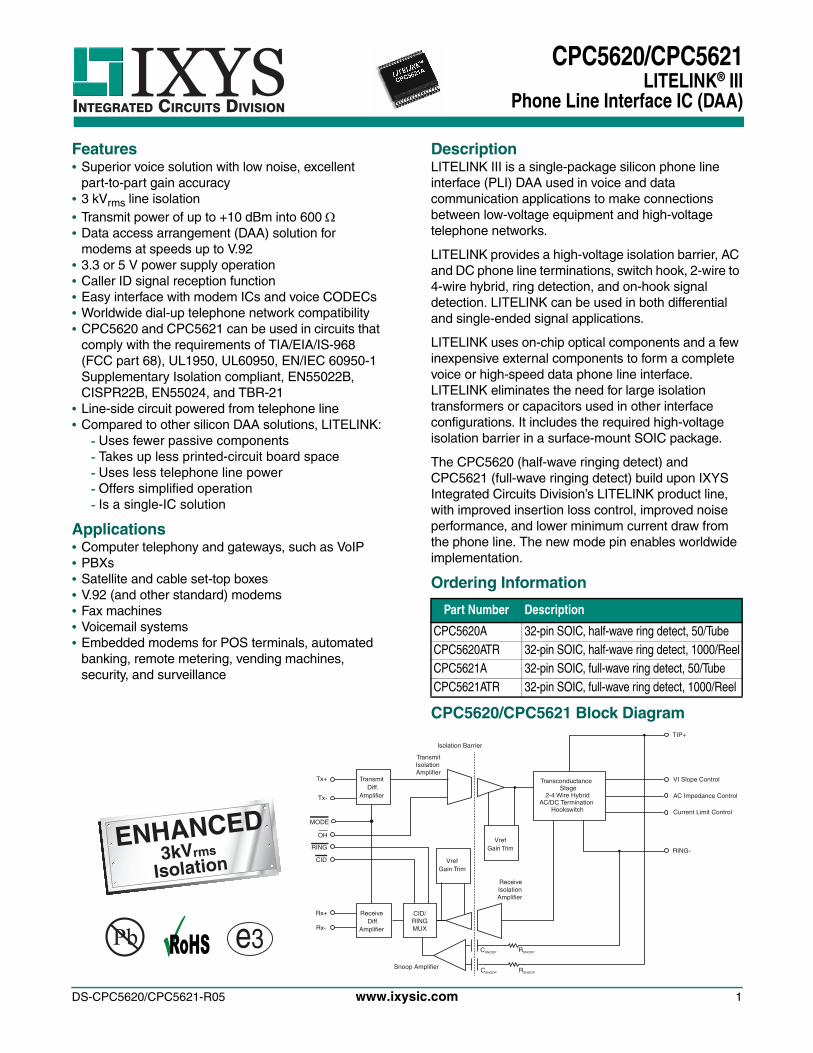
LITELINK provides a high-voltage isolation barrier, AC and DC phone line terminations, switch hook, 2-wire to 4-wire hybrid, ring detection, and on-hook signal detection. LITELINK can be used in both differential and single-ended signal applications.
LITELINK uses on-chip optical components and a few inexpensive external components to form a complete voice or high-speed data phone line interface. LITELINK eliminates the need for large isolation transformers or capacitors used in other interface configurations. It includes the required high-voltage isolation barrier in a surface-mount SOIC package.
The CPC5620 (half-wave ringing detect) and CPC5621 (full-wave ringing detect) build upon IXYS Integrated Circuits Division’s LITELINK product line, with improved insertion loss control, improved noise performance, and lower minimum current draw from the phone line. The new mode pin enables worldwide implementation.
Ordering Information
CPC5620/CPC5621 Block Diagram
Part Number Description
CPC5620A 32-pin SOIC, half-wave ring detect, 50/TubeCPC5620ATR 32-pin SOIC, half-wave ring detect, 1000/ReelCPC5621A 32-pin SOIC, full-wave ring detect, 50/TubeCPC5621ATR 32-pin SOIC, full-wave ring detect, 1000/Reel
TransconductanceStage
2-4 Wire HybridAC/DC Termination
Hookswitch
Isolation Barrier
VrefGain Trim
VrefGain Trim
Snoop Amplifier
ReceiveIsolationAmplifier
TransmitIsolationAmplifier
TIP+
RING-
TransmitDiff.
Amplifier
ReceiveDiff.
Amplifier
CID/RINGMUX
Tx+
Tx-
OH
RING
MODE
CID
Rx+
Rx-
Current Limit Control
AC Impedance Control
VI Slope Control
CSNOOP
CSNOOP
RSNOOP
RSNOOP
CPC5620/CPC5621LITELINK® III
Phone Line Interface IC (DAA)
INTEGRATED CIRCUITS DIVISION CPC5620/CPC5621
2 www.ixysic.com R05
1 Electrical Specifications. . . . . . . . . . . . . . . . . . . . . . . . . . . . . . . . . . . . . . . . . . . . . . . . . . . . . . . . . . . . . . . . . . . 31.1 Absolute Maximum Ratings. . . . . . . . . . . . . . . . . . . . . . . . . . . . . . . . . . . . . . . . . . . . . . . . . . . . . . . . . . . . . 31.2 Performance . . . . . . . . . . . . . . . . . . . . . . . . . . . . . . . . . . . . . . . . . . . . . . . . . . . . . . . . . . . . . . . . . . . . . . . . 41.3 Pin Description . . . . . . . . . . . . . . . . . . . . . . . . . . . . . . . . . . . . . . . . . . . . . . . . . . . . . . . . . . . . . . . . . . . . . . 5
2 Application Circuits . . . . . . . . . . . . . . . . . . . . . . . . . . . . . . . . . . . . . . . . . . . . . . . . . . . . . . . . . . . . . . . . . . . . . . 62.1 Resistive Termination Application Circuit . . . . . . . . . . . . . . . . . . . . . . . . . . . . . . . . . . . . . . . . . . . . . . . . . . 6
2.1.1 Resistive Termination Application Circuit Part List . . . . . . . . . . . . . . . . . . . . . . . . . . . . . . . . . . . . . . 72.1.2 Reactive Termination Application Circuit Part List . . . . . . . . . . . . . . . . . . . . . . . . . . . . . . . . . . . . . . . 9
3 Using LITELINK. . . . . . . . . . . . . . . . . . . . . . . . . . . . . . . . . . . . . . . . . . . . . . . . . . . . . . . . . . . . . . . . . . . . . . . . . 103.1 Switch Hook Control (On-hook and Off-hook States) . . . . . . . . . . . . . . . . . . . . . . . . . . . . . . . . . . . . . . . . 103.2 On-hook Operation: OH=1. . . . . . . . . . . . . . . . . . . . . . . . . . . . . . . . . . . . . . . . . . . . . . . . . . . . . . . . . . . . . 10
3.2.1 Ringing Signal Reception via the Snoop Circuit. . . . . . . . . . . . . . . . . . . . . . . . . . . . . . . . . . . . . . . . 103.2.2 Polarity Reversal Detection with CPC5621 in On-hook State . . . . . . . . . . . . . . . . . . . . . . . . . . . . . 113.2.3 On-hook Caller ID Signal Reception . . . . . . . . . . . . . . . . . . . . . . . . . . . . . . . . . . . . . . . . . . . . . . . . 11
3.3 Off-Hook Operation: OH=0 . . . . . . . . . . . . . . . . . . . . . . . . . . . . . . . . . . . . . . . . . . . . . . . . . . . . . . . . . . . . 123.3.1 Receive Signal Path. . . . . . . . . . . . . . . . . . . . . . . . . . . . . . . . . . . . . . . . . . . . . . . . . . . . . . . . . . . . . 123.3.2 Transmit Signal Path . . . . . . . . . . . . . . . . . . . . . . . . . . . . . . . . . . . . . . . . . . . . . . . . . . . . . . . . . . . . 12
3.4 Start-up Requirements . . . . . . . . . . . . . . . . . . . . . . . . . . . . . . . . . . . . . . . . . . . . . . . . . . . . . . . . . . . . . . . 133.5 DC Characteristics. . . . . . . . . . . . . . . . . . . . . . . . . . . . . . . . . . . . . . . . . . . . . . . . . . . . . . . . . . . . . . . . . . . 13
3.5.1 Setting a Current Limit . . . . . . . . . . . . . . . . . . . . . . . . . . . . . . . . . . . . . . . . . . . . . . . . . . . . . . . . . . . 133.6 AC Characteristics. . . . . . . . . . . . . . . . . . . . . . . . . . . . . . . . . . . . . . . . . . . . . . . . . . . . . . . . . . . . . . . . . . . 13
3.6.1 Resistive Termination Applications . . . . . . . . . . . . . . . . . . . . . . . . . . . . . . . . . . . . . . . . . . . . . . . . . 133.6.2 Reactive Termination Applications. . . . . . . . . . . . . . . . . . . . . . . . . . . . . . . . . . . . . . . . . . . . . . . . . . 133.6.3 Mode Pin Usage. . . . . . . . . . . . . . . . . . . . . . . . . . . . . . . . . . . . . . . . . . . . . . . . . . . . . . . . . . . . . . . . 14
4 Regulatory Information . . . . . . . . . . . . . . . . . . . . . . . . . . . . . . . . . . . . . . . . . . . . . . . . . . . . . . . . . . . . . . . . . . 14
5 LITELINK Design Resources . . . . . . . . . . . . . . . . . . . . . . . . . . . . . . . . . . . . . . . . . . . . . . . . . . . . . . . . . . . . . . 14
6 LITELINK Performance. . . . . . . . . . . . . . . . . . . . . . . . . . . . . . . . . . . . . . . . . . . . . . . . . . . . . . . . . . . . . . . . . . . 15
7 Manufacturing Information. . . . . . . . . . . . . . . . . . . . . . . . . . . . . . . . . . . . . . . . . . . . . . . . . . . . . . . . . . . . . . . . 177.1 Mechanical Dimensions. . . . . . . . . . . . . . . . . . . . . . . . . . . . . . . . . . . . . . . . . . . . . . . . . . . . . . . . . . . . . . . 18
INTEGRATED CIRCUITS DIVISION CPC5620/CPC5621
1. Electrical Specifications
1.1 Absolute Maximum RatingsAbsolute maximum ratings are stress ratings. Stresses in excess of these ratings can cause permanent damage to the device. Functional operation of the device at conditions beyond those indicated in the operational sections of this data sheet is not implied.
Parameter Minimum Maximum Unit
VDD -0.3 6 V
Logic Inputs -0.3 VDD + 0.3 V
Continuous Tip to RingCurrent (RZDC = 5.2) - 150 mA
Total Package Power Dissipation
- 1 W
Isolation Voltage - 3000 Vrms
Operating temperature -40 +85 °C
Storage temperature -40 +125 °C
R05 www.ixysic.com 3
INTEGRATED CIRCUITS DIVISION CPC5620/CPC5621
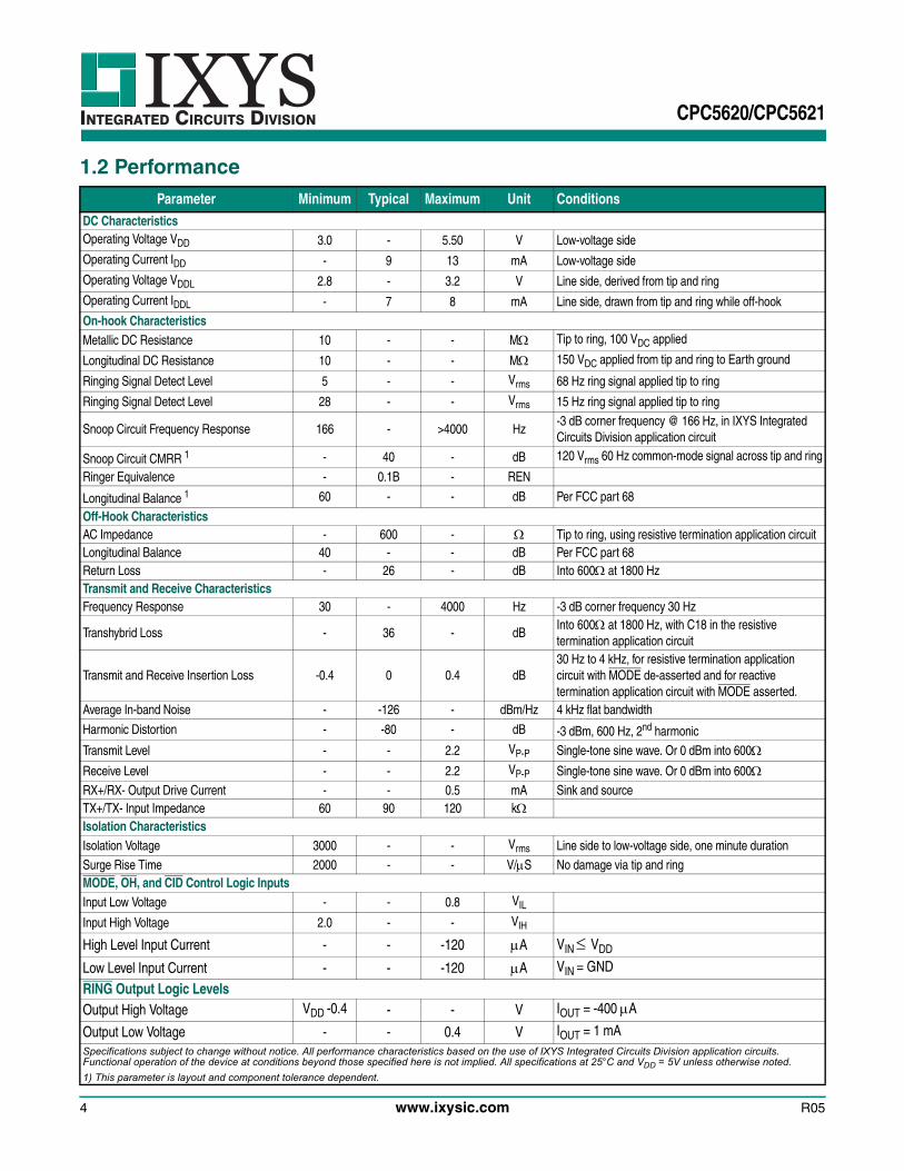
1.2 PerformanceParameter Minimum Typical Maximum Unit Conditions
DC CharacteristicsOperating Voltage VDD 3.0 - 5.50 V Low-voltage side
Operating Current IDD - 9 13 mA Low-voltage side
Operating Voltage VDDL 2.8 - 3.2 V Line side, derived from tip and ring
Operating Current IDDL - 7 8 mA Line side, drawn from tip and ring while off-hook
On-hook CharacteristicsMetallic DC Resistance 10 - - M Tip to ring, 100 VDC applied
Longitudinal DC Resistance 10 - - M 150 VDC applied from tip and ring to Earth ground
Ringing Signal Detect Level 5 - - Vrms 68 Hz ring signal applied tip to ring
Ringing Signal Detect Level 28 - - Vrms 15 Hz ring signal applied tip to ring
Snoop Circuit Frequency Response 166 - >4000 Hz-3 dB corner frequency @ 166 Hz, in IXYS Integrated Circuits Division application circuit
Snoop Circuit CMRR 1 - 40 - dB 120 Vrms 60 Hz common-mode signal across tip and ring
Ringer Equivalence - 0.1B - REN
Longitudinal Balance 1 60 - - dB Per FCC part 68
Off-Hook CharacteristicsAC Impedance - 600 - Tip to ring, using resistive termination application circuitLongitudinal Balance 40 - - dB Per FCC part 68Return Loss - 26 - dB Into 600 at 1800 HzTransmit and Receive CharacteristicsFrequency Response 30 - 4000 Hz -3 dB corner frequency 30 Hz
Transhybrid Loss - 36 - dBInto 600 at 1800 Hz, with C18 in the resistive termination application circuit
Transmit and Receive Insertion Loss -0.4 0 0.4 dB30 Hz to 4 kHz, for resistive termination application circuit with MODE de-asserted and for reactive termination application circuit with MODE asserted.
Average In-band Noise - -126 - dBm/Hz 4 kHz flat bandwidth
Harmonic Distortion - -80 - dB -3 dBm, 600 Hz, 2nd harmonic
Transmit Level - - 2.2 VP-P Single-tone sine wave. Or 0 dBm into 600
Receive Level - - 2.2 VP-P Single-tone sine wave. Or 0 dBm into 600RX+/RX- Output Drive Current - - 0.5 mA Sink and sourceTX+/TX- Input Impedance 60 90 120 kIsolation CharacteristicsIsolation Voltage 3000 - - Vrms Line side to low-voltage side, one minute duration
Surge Rise Time 2000 - - V/S No damage via tip and ringMODE, OH, and CID Control Logic InputsInput Low Voltage - - 0.8 VIL
Input High Voltage 2.0 - - VIH
High Level Input Current - - -120 A VIN VDD
Low Level Input Current - - -120 A VIN = GND
RING Output Logic LevelsOutput High Voltage VDD -0.4 - - V IOUT = -400 A
Output Low Voltage - - 0.4 V IOUT = 1 mASpecifications subject to change without notice. All performance characteristics based on the use of IXYS Integrated Circuits Division application circuits. Functional operation of the device at conditions beyond those specified here is not implied. All specifications at 25°C and VDD = 5V unless otherwise noted.
1) This parameter is layout and component tolerance dependent.
4 www.ixysic.com R05
INTEGRATED CIRCUITS DIVISION CPC5620/CPC5621
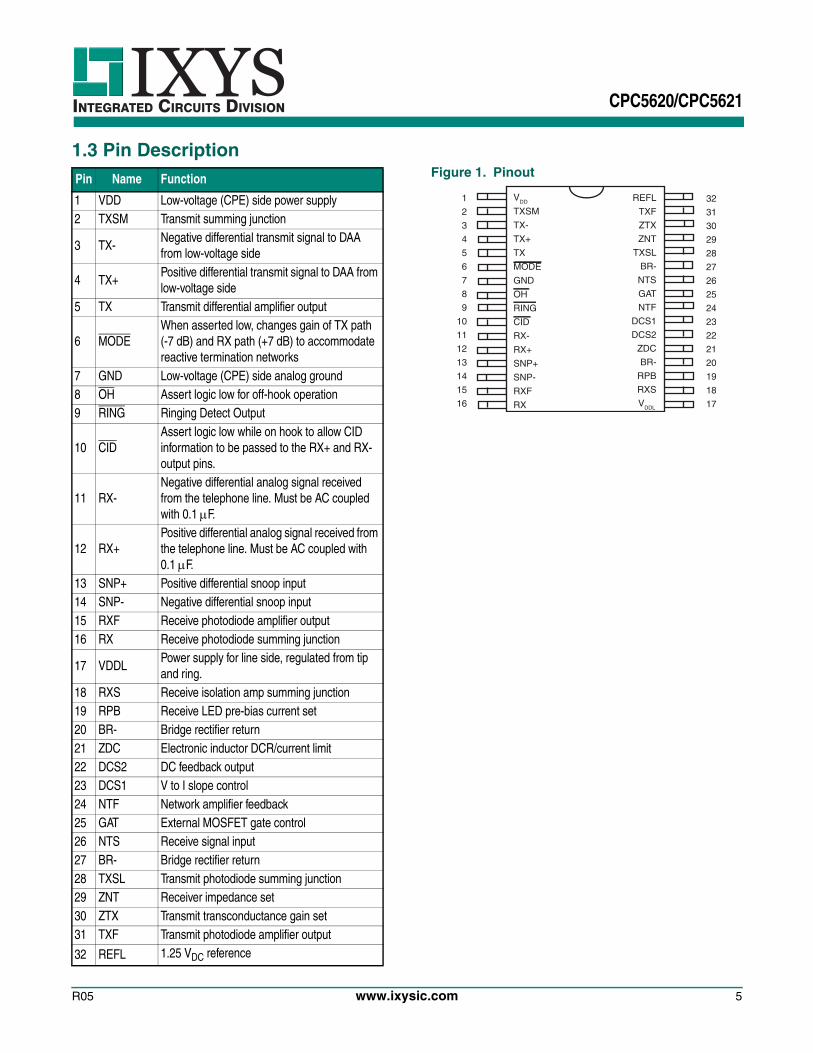
1.3 Pin DescriptionFigure 1. PinoutPin Name Function
1 VDD Low-voltage (CPE) side power supply2 TXSM Transmit summing junction
3 TX-Negative differential transmit signal to DAA from low-voltage side
4 TX+Positive differential transmit signal to DAA from low-voltage side
5 TX Transmit differential amplifier output
6 MODEWhen asserted low, changes gain of TX path(-7 dB) and RX path (+7 dB) to accommodate reactive termination networks
7 GND Low-voltage (CPE) side analog ground8 OH Assert logic low for off-hook operation9 RING Ringing Detect Output
10 CIDAssert logic low while on hook to allow CID information to be passed to the RX+ and RX- output pins.
11 RX-Negative differential analog signal received from the telephone line. Must be AC coupled with 0.1 F.
12 RX+Positive differential analog signal received from the telephone line. Must be AC coupled with 0.1 F.
13 SNP+ Positive differential snoop input14 SNP- Negative differential snoop input15 RXF Receive photodiode amplifier output16 RX Receive photodiode summing junction
17 VDDLPower supply for line side, regulated from tip and ring.
18 RXS Receive isolation amp summing junction19 RPB Receive LED pre-bias current set20 BR- Bridge rectifier return21 ZDC Electronic inductor DCR/current limit22 DCS2 DC feedback output23 DCS1 V to I slope control24 NTF Network amplifier feedback25 GAT External MOSFET gate control26 NTS Receive signal input27 BR- Bridge rectifier return28 TXSL Transmit photodiode summing junction29 ZNT Receiver impedance set30 ZTX Transmit transconductance gain set31 TXF Transmit photodiode amplifier output
32 REFL 1.25 VDC reference
1
2
3
4
5
6
7
8
9
10
11
12
13
14
15
16
32
31
30
29
28
27
26
25
24
23
22
21
20
19
18
17
VDD
TXSM
TX-
TX+
TX
MODE
GND
OH
RING
CID
RX-
RX+
SNP+
SNP-
RXF
RX
REFL
TXF
ZTX
ZNT
TXSL
BR-
NTS
GAT
NTF
DCS1
DCS2
ZDC
BR-
RPB
RXS
VDDL
R05 www.ixysic.com 5
INTEGRATED CIRCUITS DIVISION CPC5620/CPC5621
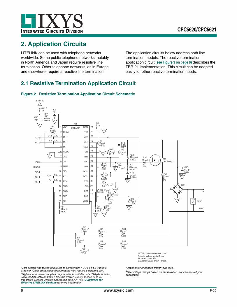
2. Application CircuitsLITELINK can be used with telephone networks worldwide. Some public telephone networks, notably in North America and Japan require resistive line termination. Other telephone networks, as in Europe and elsewhere, require a reactive line termination.
The application circuits below address both line termination models. The reactive termination application circuit (see Figure 3 on page 8) describes the TBR-21 implementation. This circuit can be adapted easily for other reactive termination needs.
2.1 Resistive Termination Application Circuit
Figure 2. Resistive Termination Application Circuit Schematic
¹This design was tested and found to comply with FCC Part 68 with this Sidactor. Other compliance requirements may require a different part.²Higher-noise power supplies may require substitution of a 220 H inductor, Toko 380HB-2215 or similar. See the Power Quality section of IXYS Integrated Circuits Division application note AN-146, Guidelines for Effective LITELINK Designs for more information.
³Optional for enhanced transhybrid loss.4Use voltage ratings based on the isolation requirements of your application.
+
-
OH
RING
TX+
RX+
TX-
RX-
3.3 or 5V
C13
C14
C2
C4
R1(RTX)80.6K
R23 210
BR-
BR-
BR-
TIP
RING
U1
LITELINK1
2
3
4
5
6
7
8
9
10
11
12
13
14
15
16
32
31
30
29
28
27
26
25
24
23
22
21
20
19
18
17
VDD
TXSM
TX-
TX+
TX
GND
RX-
RX+
SNP+
SNP-
RXF
RX
MODE
OH
RING
CID
REFL
TXF
ZTX
ZNT
TXSL
BR-
NTS
GAT
NTF
DCS1
DCS2
ZDC
BR-
RPB
RXS
VDDL
DB1
SP1 1BR-
BR-
A
A
AC90.1μ
C1610μ
FB1600 Ω
200 mA
C11μ
(RTXF)60.4K
5%
(RHTF)200K
R13(RNTS)1M
5%
C100.01μ500V
R15
1.69M
R20
2
6.49M
(RDCS1A)6.49 M
(CDCS)0.027μ
(RRXF)130K
R3
1.5M
C7(CSNP-)
4
220pF
C8
220pF
(RSNP-2)
1.8M 1.8M
1.8M 1.8M
R4
68.1BR-
NOTE: Unless otherwise noted:Resistor values are in Ohms All resistors are 1%.Capacitor values are in Farads.
R14(RGAT)
47
Q1CPC5602C
(CGAT)
(RZDC) 38.2
R10
301
R18
3.32KC1815p 3
R12
499K
(RNTF)
BR-
BR-
C150.01μ500V
221K
(RNTX)261K
0.1μ
0.1μ
0.1μ
0.1μ
R16
R8
R5
R75BR-
C21100p
R76
R22
R21
C12
R6 R44
R7 R45
(RSNP-1)
(RSNP+2) (RSNP+1)
(RSNPD)
(RDCS1B)
(RHTX)
(RZNT)
(RZTX)
(RPB)
(RDCS2) (RVDDL)
BR-
(CSNP+) 4
R2
CID
6 www.ixysic.com R05
INTEGRATED CIRCUITS DIVISION CPC5620/CPC5621
2.1.1 Resistive Termination Application Circuit Part ListQuantity Reference Designator Description Supplier(s)
1 C1 1 F, 16 V, ±10%
AVX, Murata, Novacap, Panasonic, SMEC, Tecate, etc.
5 C2, C4, C9, C13, C14 0.1 F, 16 V, ±10%
2 C7, C8 1 220 pF, ±5%
2 C10, C15 0.01 F, 500 V, ±10%1 C12 0.027 F, 16 V, ±10%1 C16 10 F, 16 V, ±10%1 C18 (optional) 15 pF, 16 V, ±10%1 C21 100 pF, 16 V, 10%1 R1 80.6 k, 1/16 W, ±1%
Panasonic, Electro Films, FMI, Vishay, etc.
1 R2 130 k, 1/16 W, ±1%1 R3 1.5 M, 1/16 W, ±1%1 R4 68.1 , 1/16 W, ±1%1 R5 60.4 k, 1/16 W, ±1%
4 R6, R7, R44, R45 2 1.8 M, 1/10 W, ±1%
1 R8 221 k, 1/16 W, ±1%1 R10 301 , 1/16 W, ±1%1 R12 499 k, 1/16 W, ±1%1 R13 1 M, 1/16 W, ±1%1 R14 47 , 1/16 W, ±5%1 R15 1.69 M, 1/16 W, ±1%1 R16 8.2 , 1/8 W, ±1%1 R18 3.32 k 1/16 W, ±1%1 R20 2 , 1/16 W, ±5%1 R21, R22 6.49 M, 1/16 W, ±1%1 R23 10 1/16 W, ±5%, or 220 H inductor1 R75 261 k, 1/16 W, ±1%1 R76 200 k, 1/16 W, ±1%1 FB1 600 , 200 mA ferrite bead Murata BLM11A601S or similar1 DB1 S1ZB60 bridge rectifier Shindengen, Diodes, Inc.
1 SP1 350 V Bourns (TISP4350H3) or Teccor (P3100SC)
1 Q1 CPC5602 FETIXYS Integrated Circuits Division
1 U1 CPC5620/CPC5621 LITELINK1Use voltage ratings based on the isolation requirements of your application. Typical applications will require 2kV to safely hold off the isolation voltage.2Use components that allow enough space to account for the possibility of high-voltage arcing.
R05 www.ixysic.com 7
INTEGRATED CIRCUITS DIVISION CPC5620/CPC5621
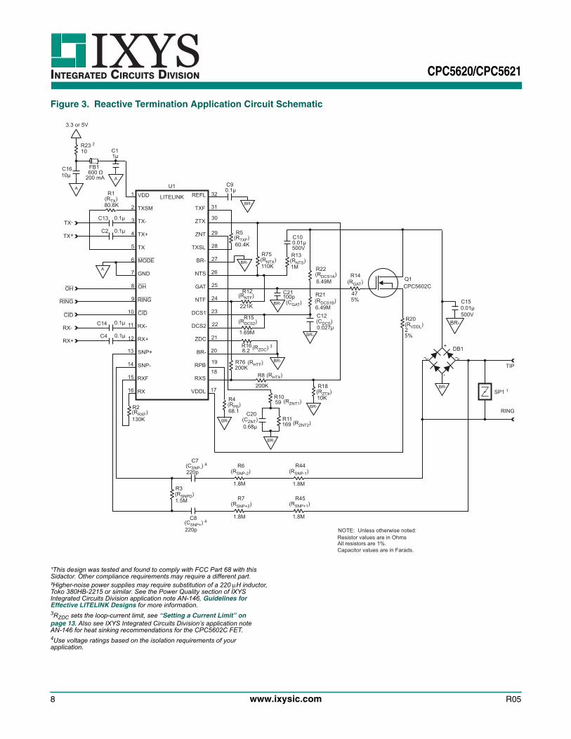
Figure 3. Reactive Termination Application Circuit Schematic
¹This design was tested and found to comply with FCC Part 68 with this Sidactor. Other compliance requirements may require a different part.²Higher-noise power supplies may require substitution of a 220 H inductor, Toko 380HB-2215 or similar. See the Power Quality section of IXYS Integrated Circuits Division application note AN-146, Guidelines for Effective LITELINK Designs for more information.3RZDC sets the loop-current limit, see “Setting a Current Limit” on page 13. Also see IXYS Integrated Circuits Division’s application note AN-146 for heat sinking recommendations for the CPC5602C FET.4Use voltage ratings based on the isolation requirements of your application.
+
-
OH
RING
TX+
RX+
TX-
RX-
3.3 or 5V
C13
C14
C2
C4
R1(RTX)80.6K
R23 210
BR-
BR-
BR-
TIP
RING
U1
LITELINK1
2
3
4
5
6
7
8
9
10
11
12
13
14
15
16
32
31
30
29
28
27
26
25
24
23
22
21
20
19
18
17
VDD
TXSM
TX-
TX+
TX
GND
RX-
RX+
SNP+
SNP-
RXF
RX
MODE
OH
RING
REFL
TXF
ZTX
ZNT
TXSL
BR-
NTS
GAT
NTF
DCS1
DCS2
ZDC
BR-
RPB
RXS
VDDL
DB1
SP1 1BR-
BR-
A
A
AC90.1μ
C1610μ
FB1600 Ω
200 mA
C11μ
(RTXF)60.4K
5%
(RHTF)200K
R13(RNTS)1M
5%
C100.01μ500V
R15
1.69M
R20
2
6.49M
(RDCS1A)6.49M
(CDCS)0.027μ
(RRXF)130K
R3
1.5M
C7(CSNP-)
4
220p
C8
220p
(RSNP-2)
1.8M 1.8M
1.8M 1.8M
R4
68.1
BR-
NOTE: Unless otherwise noted:Resistor values are in Ohms All resistors are 1%.Capacitor values are in Farads.
R14(RGAT)
47
Q1CPC5602C
(CGAT)
(RZDC) 38.2
R1059
R18
10K
R11169
C20(CZNT)0.68μ
R12
221K
(RNTF)
BR-
BR-
C150.01μ500V
200K
(RNTX)110K
0.1μ
0.1μ
0.1μ
0.1μ
R16
R8
R5
R75BR-
C21100p
R76
R22
R21
C12
R6 R44
R7 R45
(RSNP-1)
(RSNP+2) (RSNP+1)
(RSNPD)
(RDCS1B)
(RHTX)
(RZNT1)
(RZTX)
(RPB)
(RZNT2)
(RDCS2) (RVDDL)
BR-
(CSNP+) 4
R2
CID CID
8 www.ixysic.com R05
INTEGRATED CIRCUITS DIVISION CPC5620/CPC5621
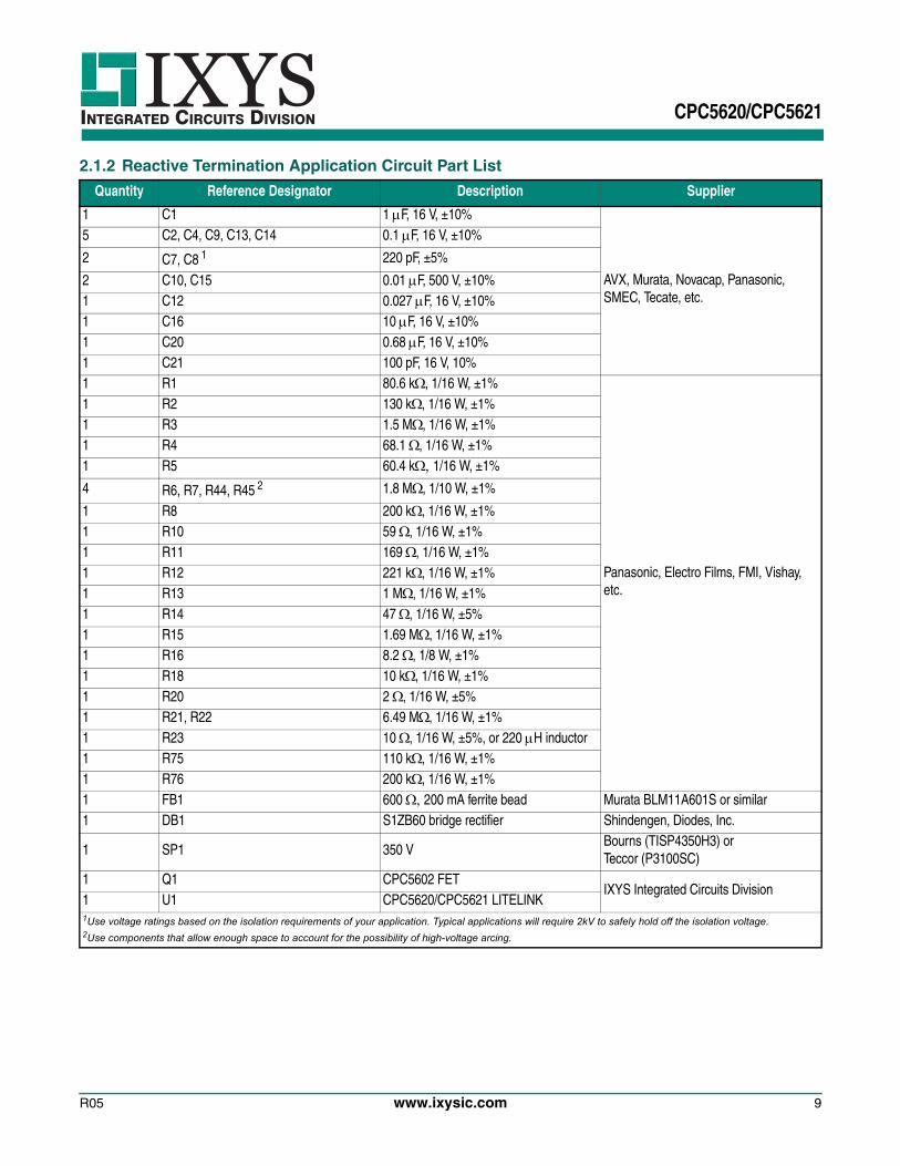
2.1.2 Reactive Termination Application Circuit Part List
Quantity Reference Designator Description Supplier
1 C1 1 F, 16 V, ±10%
AVX, Murata, Novacap, Panasonic, SMEC, Tecate, etc.
5 C2, C4, C9, C13, C14 0.1 F, 16 V, ±10%
2 C7, C8 1 220 pF, ±5%
2 C10, C15 0.01 F, 500 V, ±10%1 C12 0.027 F, 16 V, ±10%1 C16 10 F, 16 V, ±10%1 C20 0.68 F, 16 V, ±10%1 C21 100 pF, 16 V, 10%1 R1 80.6 k, 1/16 W, ±1%
Panasonic, Electro Films, FMI, Vishay, etc.
1 R2 130 k, 1/16 W, ±1%1 R3 1.5 M, 1/16 W, ±1%1 R4 68.1 , 1/16 W, ±1%1 R5 60.4 k 1/16 W, ±1%
4 R6, R7, R44, R45 2 1.8 M, 1/10 W, ±1%
1 R8 200 k, 1/16 W, ±1%1 R10 59 , 1/16 W, ±1%1 R11 169 , 1/16 W, ±1%1 R12 221 k, 1/16 W, ±1%1 R13 1 M, 1/16 W, ±1%1 R14 47 , 1/16 W, ±5%1 R15 1.69 M, 1/16 W, ±1%1 R16 8.2 , 1/8 W, ±1%1 R18 10 k, 1/16 W, ±1%1 R20 2 , 1/16 W, ±5%1 R21, R22 6.49 M, 1/16 W, ±1%1 R23 10 , 1/16 W, ±5%, or 220 H inductor1 R75 110 k, 1/16 W, ±1%1 R76 200 k, 1/16 W, ±1%1 FB1 600 200 mA ferrite bead Murata BLM11A601S or similar1 DB1 S1ZB60 bridge rectifier Shindengen, Diodes, Inc.
1 SP1 350 VBourns (TISP4350H3) or Teccor (P3100SC)
1 Q1 CPC5602 FETIXYS Integrated Circuits Division
1 U1 CPC5620/CPC5621 LITELINK1Use voltage ratings based on the isolation requirements of your application. Typical applications will require 2kV to safely hold off the isolation voltage.2Use components that allow enough space to account for the possibility of high-voltage arcing.
R05 www.ixysic.com 9
INTEGRATED CIRCUITS DIVISION CPC5620/CPC5621
3. Using LITELINKAs a full-featured telephone line interface, LITELINK performs the following functions:
• DC termination and V/I slope control• AC impedance control• 2-wire to 4-wire conversion (hybrid)• Current limiting• Ringing signal reception• Caller ID signaling reception• Switch hook
LITELINK can accommodate specific application features without sacrificing basic functionality and performance. Application features include, but are not limited to:
• High transmit power operation• Pulse dialing• Ground start• Loop start• Parallel telephone off-hook detection (line intrusion)• Battery reversal detection• Line presence detection• World-wide programmable operation
This section of the data sheet describes LITELINK operation in standard configuration for usual operation. IXYS Integrated Circuits Division offers additional application information on-line (see Section 5 on page 14). These include information on the following topics:
• Circuit isolation considerations• Optimizing LITELINK performance• Data Access Arrangement architecture• LITELINK circuit descriptions• Surge protection• EMI considerations
Other specific application materials are also referenced in this section as appropriate.
3.1 Switch Hook Control (On-hook and Off-hook States)LITELINK operates in one of two conditions, on-hook and off-hook. In the on-hook condition the telephone line is available for calls. In the off-hook condition the telephone line is engaged. The OH control input is used to place LITELINK in one of these two states.
With OH high, LITELINK is on-hook and ready to make or receive a call. While on-hook, the CID control is used to select between passing the caller-ID tones from Tip and Ring to the RX+ and RX- outputs and the ringing detect function. Setting CID to a logic low enables the CID path while placing CID to a logic high configures the LITELINK to detect ringing.
Asserting OH low causes LITELINK to answer or originate a call by entering the off-hook state. In the off-hook state, loop current flows through LITELINK.
3.2 On-hook Operation: OH=1The LITELINK application circuit leakage current is less than 10 A with 100 V across ring and tip, equivalent to greater than 10 M on-hook resistance.
3.2.1 Ringing Signal Reception via the Snoop Circuit
In the on-hook state (OH and CID not asserted), an internal multiplexer turns on the snoop circuit. This circuit monitors the telephone line for two conditions; an incoming ring signal, and caller ID data bursts.
Refer to the application schematic diagram (see Figure 2. on page 6). C7 (CSNP-) and C8 (CSNP+) provide a high-voltage isolation barrier between the telephone line and SNP- and SNP+ on the LITELINK while coupling AC signals to the snoop amplifier. The snoop circuit “snoops” the telephone line continuously while drawing no current. In the LITELINK, ringing signals are compared to a threshold. The comparator output forms the RING signal output from LITELINK. This signal must be qualified by the host system as a valid ringing signal. A low level on RING indicates that the LITELINK ring signal threshold has been exceeded.
For the CPC5620 (with the half-wave ring detector), the frequency of the RING output follows the frequency of the ringing signal from the central office (CO), typically 20 Hz. The RING output of the CPC5621 (with the full-wave ring detector) is twice the ringing signal frequency.
Hysteresis is employed in the LITELINK ring detector circuit to provide noise immunity. The set-up of the ring detector comparator causes RING output pulses to remain low for most of the ringing signal half-cycle. The RING output returns high for the entire negative
10 www.ixysic.com R05
INTEGRATED CIRCUITS DIVISION CPC5620/CPC5621
half-cycle of the ringing signal for the CPC5620. For the CPC5621, the RING output returns high for a short period near the zero-crossing of the ringing signal before returning low during the positive half-cycle. For both the CPC5620 and CPC5621, the RING output remains high between ringing signal bursts.
The ringing detection threshold depends on the values of R3 (RSNPD), R6 & R44 (RSNP-), R7 & R45 (RSNP+), C7 (CSNP-), and C8 (CSNP+). The value of these components shown in the application circuits are recommended for typical operation. The ringing detection threshold can be changed according to the following formula:
Where:
• RSNPD = R3 in the application circuits shown in this data sheet.
• RSNPTOTAL = the total of R6, R7, R44, and R45 in the application circuits shown in this data sheet.
• CSNP = C7 = C8 in the application circuits shown in this data sheet.
• And ƒRING is the frequency of the ringing signal.
IXYS Integrated Circuits Division Application Note AN-117 Customize Caller ID Gain and Ring Detect Voltage Threshold is a spreadsheet for trying different component values in this circuit. Changing the ringing detection threshold will also change the caller ID gain and the timing of the polarity reversal detection pulse, if used.
3.2.2 Polarity Reversal Detection with CPC5621 in On-hook State
The full-wave ringing detector in the CPC5621 makes it possible to detect on-hook tip and ring polarity reversal using the RING output. When the polarity of tip and ring reverses, a pulse on RING indicates the event. Your system logic must be able to discriminate this single pulse of approximately 1 msec (using the recommended snoop circuit external components) from a valid ringing signal.
3.2.3 On-hook Caller ID Signal ReceptionOn-hook caller ID (CID) signals are processed by LITELINK by coupling the CID data burst through the snoop circuit to the LITELINK RX outputs under control of the CID pin. In North America, CID data signals are typically sent between the first and second ringing signal.
In North American applications, follow these steps to receive on-hook caller ID data via the LITELINK RX outputs:
1. Detect the first ringing signal outputs on RING.2. Assert CID low.3. Process the CID data from the RX outputs.4. De-assert CID (high or floating).
Note: Taking LITELINK off-hook (via the OH pin) disconnects the snoop path from both the receive outputs and the RING output, regardless of the state of the CID pin.
CID gain from tip and ring to RX+ and RX- is determined by:
Where:
• RSNPD = R3 in the application circuits in this data sheet
• RSNPTOTAL = the total of R6, R7, R44, and R45 in the application circuits in this data sheet
• CSNP = C7 = C8 in the application circuits in this data sheet
• and where ƒ is the frequency of the CID signal
The recommended components in the application circuit yield a gain 0.27 dB at 2000 Hz. IXYS Integrated Circuits Division Application Note AN-117 Customize Caller ID Gain and Ring Detect Voltage Threshold is a spreadsheet for trying different component values in this circuit. Changing the CID gain will also change the ring detection threshold and the timing of the polarity reversal detection pulse, if used.
VRINGPK750mVRSNPD----------------- RSNPTOTAL RSNPD+ 2 1
fRINGCSNP 2--------------------------------------+=
GAINCID dB 206RSNPD
RSNPTOTAL RSNPD+ 2 1
fCSNP 2--------------------------+
-------------------------------------------------------------------------------------------------log=
R05 www.ixysic.com 11
INTEGRATED CIRCUITS DIVISION CPC5620/CPC5621
For single-ended receive applications where only one RX output is used, the snoop circuit gain can be adjusted back to 0 dB by changing the value of the snoop series resistors R6, R7, R44 and R45 from 1.8M to 715k This change results in negligible modification to the ringing detect threshold.
3.3 Off-Hook Operation: OH=0
3.3.1 Receive Signal PathSignals to and from the telephone network appear on the tip and ring connections of the application circuit. Receive signals are extracted from transmit signals by the LITELINK two-wire to four-wire hybrid. Next, the receive signal is converted to infrared light by the receive photodiode amplifier and receive path LED. The intensity of the light is modulated by the receive signal and coupled across the electrical isolation barrier by a reflective dome.
On the equipment’s low voltage side of the barrier, the receive signal is converted by a photodiode into a photocurrent. The photocurrent, a linear representation of the receive signal, is amplified and converted to a differential voltage output on RX+ and RX-.
Variations in gain are controlled to within ±0.4 dB by factory gain trim, which sets the output to unity gain.
To accommodate single-supply operation, LITELINK includes a small DC bias on the RX outputs of 1.0VDC. Most applications should AC couple the RX outputs as shown in Figure 4.
LITELINK may be used for differential or single-ended output as shown in Figure 4. Single-ended use will produce 6 dB less signal output amplitude. Do not exceed 0 dBm into 600 (2.2 VP-P) signal input with the standard application circuit. See application note AN-157, Increased LITELINK III Transmit Power for more information.
Figure 4. Differential and Single-ended Receive Path Connections to LITELINK
3.3.2 Transmit Signal PathConnect transmit signals from the low-voltage side equipment to the TX+ and TX- pins of LITELINK. Do not exceed a signal level of 0 dBm in 600 (or 2.2 VP-P). Differential transmit signals are converted to single-ended signals in LITELINK. The signal is coupled to the transmit photodiode amplifier in a similar manner to the receive path. See application note AN-157, Increased LITELINK III Transmit Power for more information.
The output of the photodiode amplifier is coupled to a voltage-to-current converter via a transconductance
stage where the transmit signal modulates the telephone line loop current. As in the receive path, gain is set to unity at the factory, limiting insertion loss variation to ±0.4 dB.
Differential and single-ended transmit signals into LITELINK should not exceed a signal level of 0 dBm referenced to 600 (or 2.2 VP-P). For output power levels above 0dBm consult the application note AN-157, Increased LITELINK III Transmit Power for more information.
RX+
RX-
RX+
RX+
RX
RX-
0.1µF
0.1µF
0.1µF
LITELINKLow-Voltage Side CODECor Voice Circuit
12 www.ixysic.com R05
INTEGRATED CIRCUITS DIVISION CPC5620/CPC5621
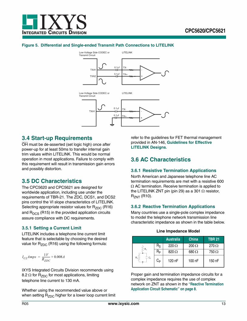
Figure 5. Differential and Single-ended Transmit Path Connections to LITELINK
3.4 Start-up RequirementsOH must be de-asserted (set logic high) once after power-up for at least 50ms to transfer internal gain trim values within LITELINK. This would be normal operation in most applications. Failure to comply with this requirement will result in transmission gain errors and possibly distortion.
3.5 DC CharacteristicsThe CPC5620 and CPC5621 are designed for worldwide application, including use under the requirements of TBR-21. The ZDC, DCS1, and DCS2 pins control the VI slope characteristics of LITELINK. Selecting appropriate resistor values for RZDC (R16) and RDCS (R15) in the provided application circuits assure compliance with DC requirements.
3.5.1 Setting a Current LimitLITELINK includes a telephone line current limit feature that is selectable by choosing the desired value for RZDC (R16) using the following formula:
IXYS Integrated Circuits Division recommends using 8.2 for RZDC for most applications, limiting telephone line current to 130 mA.
Whether using the recommended value above or when setting RZDC higher for a lower loop current limit
refer to the guidelines for FET thermal management provided in AN-146, Guidelines for Effective LITELINK Designs.
3.6 AC Characteristics
3.6.1 Resistive Termination ApplicationsNorth American and Japanese telephone line AC termination requirements are met with a resistive 600 AC termination. Receive termination is applied to the LITELINK ZNT pin (pin 29) as a 301 resistor, RZNT (R10).
3.6.2 Reactive Termination ApplicationsMany countries use a single-pole complex impedance to model the telephone network transmission line characteristic impedance as shown in the table below.
Proper gain and termination impedance circuits for a complex impedance requires the use of complex network on ZNT as shown in the “Reactive Termination Application Circuit Schematic” on page 8.
LITELINK
LITELINK
TXA1
TXA2
-
+
0.1µf
Low-Voltage Side CODEC orTransmit Circuit
Low-Voltage Side CODEC orTransmit Circuit
TX-
TX+
TXA1 -
+
TX-
TX+
0.1µf
0.1µf
0.1µf
ICLAmps1VRZDC------------- 0.008A+=
Line Impedance Model
Australia China TBR 21
RS 220 200 270 RP 820 680 750
CP 120 nF 100 nF 150 nF
RS
RP CP
R05 www.ixysic.com 13
INTEGRATED CIRCUITS DIVISION CPC5620/CPC5621
3.6.3 Mode Pin UsageAssert the MODE pin low to introduce a 7 dB pad into the transmit path and add 7 dB of gain to the receive path. These changes compensate for the gain changes made to the transmit and receive paths in reactive termination implementations.
Insertion loss with MODE de-asserted and the resistive termination application circuit is 0 dB. Insertion loss with the reactive termination application circuit and MODE asserted is also 0 dB.
4. Regulatory InformationLITELINK III can be used to build products that comply with the requirements of TIA/EIA/IS-968 (formerly FCC part 68), FCC part 15B, TBR-21, EN60950, UL1950, EN55022B, IEC950/IEC60950, CISPR22B, EN55024, and many other standards. LITELINK provides supplementary isolation. Metallic surge requirements are met through the inclusion of a Sidactor in the application circuit. Longitudinal surge protection is provided by LITELINK’s optical barrier technology and the use of high-voltage components in the application circuit as needed.
The information provided in this document is intended to inform the equipment designer but it is not sufficient to assure proper system design or regulatory compliance. Since it is the equipment manufacturer's responsibility to have their equipment properly designed to conform to all relevant regulations, designers using LITELINK are advised to carefully verify that their end-product design complies with all applicable safety, EMC, and other relevant standards and regulations. Semiconductor components are not rated to withstand electrical overstress or electro-static discharges resulting from inadequate protection measures at the board or system level.
5. LITELINK Design ResourcesThe IXYS Integrated Circuits Division web site has a wealth of information useful for designing with LITELINK, including application notes and reference designs that already meet all applicable regulatory requirements. See the following links:
LITELINK datasheets and reference designs
Application note AN-117 Customize Caller ID Gain and Ring Detect Voltage Threshold
Application note AN-146, Guidelines for Effective LITELINK Designs
Application note AN-152 LITELINK II to LITELINK III Design Conversion
Application note AN-155 Understanding LITELINK Display Feature Signal Routing and Applications
14 www.ixysic.com R05
INTEGRATED CIRCUITS DIVISION CPC5620/CPC5621
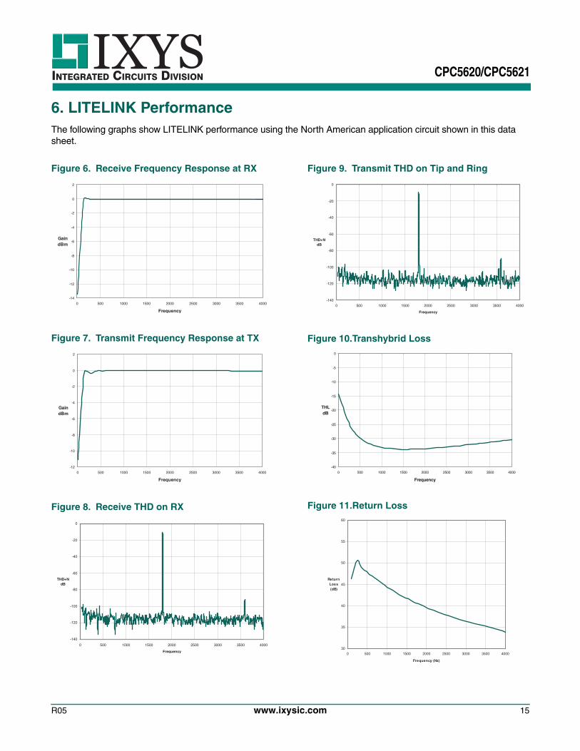
6. LITELINK PerformanceThe following graphs show LITELINK performance using the North American application circuit shown in this data sheet.
Figure 6. Receive Frequency Response at RX
Figure 7. Transmit Frequency Response at TX
Figure 8. Receive THD on RX
Figure 9. Transmit THD on Tip and Ring
Figure 10.Transhybrid Loss
Figure 11.Return Loss
-14
-12
-10
-8
-6
-4
-2
0
2
0 500 1000 1500 2000 2500 3000 3500 4000
Frequency
GaindBm
-12
-10
-8
-6
-4
-2
0
2
0 500 1000 1500 2000 2500 3000 3500 4000
Frequency
GaindBm
-140
-120
-100
-80
-60
-40
-20
0
0 500 1000 1500 2000 2500 3000 3500 4000
Frequency
THD+NdB
-140
-120
-100
-80
-60
-40
-20
0
0 500 1000 1500 2000 2500 3000 3500 4000
Frequency
THD+NdB
-40
-35
-30
-25
-20
-15
-10
-5
0
0 500 1000 1500 2000 2500 3000 3500 4000
Frequency
THLdB
30
35
40
45
50
55
60
0 500 1000 1500 2000 2500 3000 3500 4000
Frequency (Hz)
ReturnLoss(dB)
R05 www.ixysic.com 15
INTEGRATED CIRCUITS DIVISION CPC5620/CPC5621
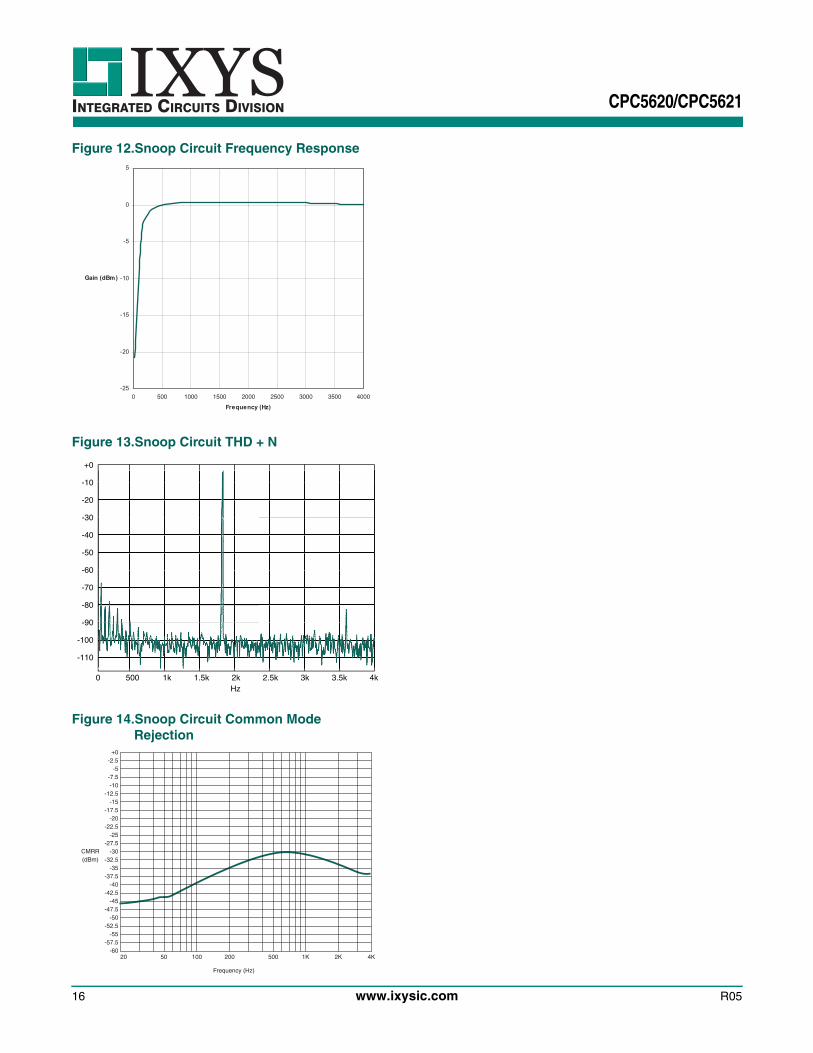
Figure 12.Snoop Circuit Frequency Response
Figure 13.Snoop Circuit THD + N
Figure 14.Snoop Circuit Common Mode Rejection
-25
-20
-15
-10
-5
0
5
0 500 1000 1500 2000 2500 3000 3500 4000
Frequency (Hz)
Gain (dBm)
Hz0 500 1k 1.5k 2k 2.5k 3k 3.5k 4k
+0
-30
-20
-10
-40
-50
-60
-70
-80
-90
-100
-110
+0-2.5
-5-7.5-10
-12.5-15
-17.5-20
-22.5-25
-27.5-30
-32.5-35
-37.5-40
-42.5-45
-47.5-50
-52.5-55
-57.5-60
CMRR(dBm)
5020 100 200 500 1K 2K 4K
Frequency (Hz)
16 www.ixysic.com R05
INTEGRATED CIRCUITS DIVISION CPC5620/CPC5621
7. Manufacturing Information
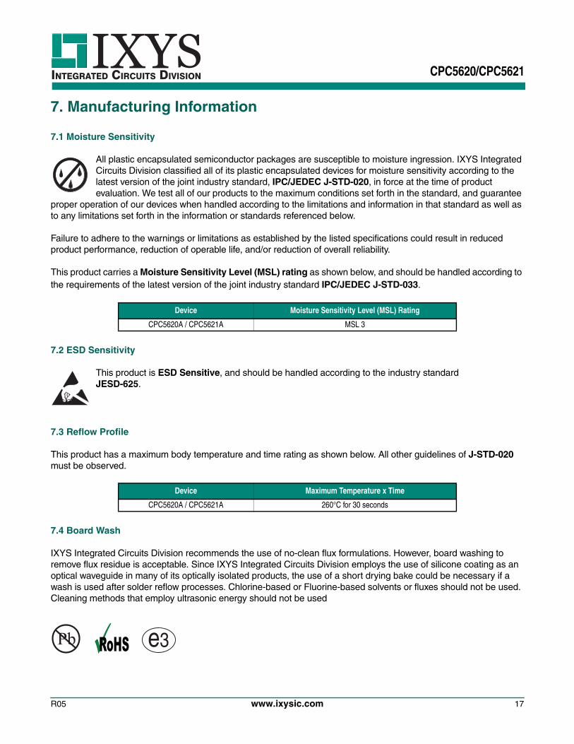
7.1 Moisture Sensitivity
All plastic encapsulated semiconductor packages are susceptible to moisture ingression. IXYS Integrated Circuits Division classified all of its plastic encapsulated devices for moisture sensitivity according to the latest version of the joint industry standard, IPC/JEDEC J-STD-020, in force at the time of product evaluation. We test all of our products to the maximum conditions set forth in the standard, and guarantee
proper operation of our devices when handled according to the limitations and information in that standard as well as to any limitations set forth in the information or standards referenced below.
Failure to adhere to the warnings or limitations as established by the listed specifications could result in reduced product performance, reduction of operable life, and/or reduction of overall reliability.
This product carries a Moisture Sensitivity Level (MSL) rating as shown below, and should be handled according to the requirements of the latest version of the joint industry standard IPC/JEDEC J-STD-033.
7.2 ESD Sensitivity
This product is ESD Sensitive, and should be handled according to the industry standard JESD-625.
7.3 Reflow Profile
This product has a maximum body temperature and time rating as shown below. All other guidelines of J-STD-020 must be observed.
7.4 Board Wash
IXYS Integrated Circuits Division recommends the use of no-clean flux formulations. However, board washing to remove flux residue is acceptable. Since IXYS Integrated Circuits Division employs the use of silicone coating as an optical waveguide in many of its optically isolated products, the use of a short drying bake could be necessary if a wash is used after solder reflow processes. Chlorine-based or Fluorine-based solvents or fluxes should not be used. Cleaning methods that employ ultrasonic energy should not be used
Device Moisture Sensitivity Level (MSL) Rating
CPC5620A / CPC5621A MSL 3
Device Maximum Temperature x Time
CPC5620A / CPC5621A 260°C for 30 seconds
e3Pb
R05 www.ixysic.com 17
INTEGRATED CIRCUITS DIVISION CPC5620/CPC5621
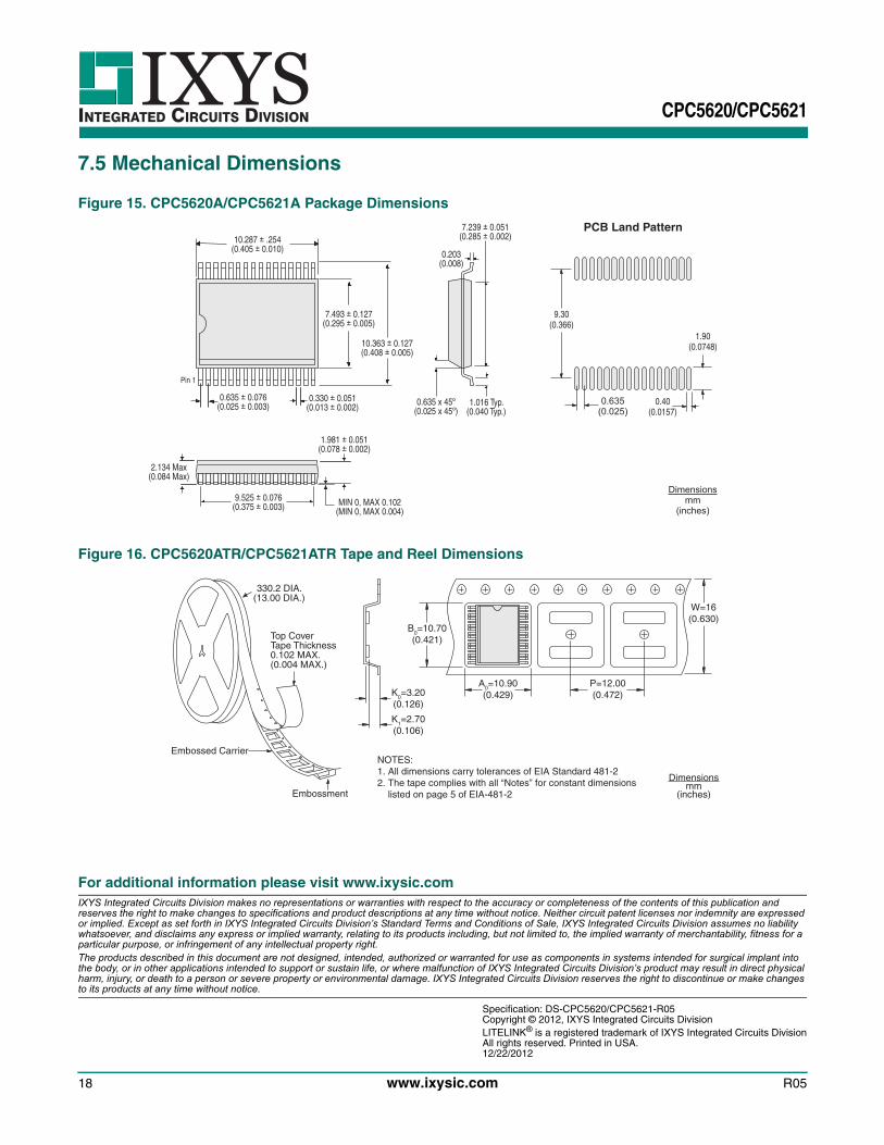
7.5 Mechanical Dimensions
Figure 15. CPC5620A/CPC5621A Package Dimensions
Figure 16. CPC5620ATR/CPC5621ATR Tape and Reel Dimensions
Dimensionsmm
(inches)
PCB Land Pattern
Pin 1
10.287 ± .254(0.405 ± 0.010)
7.493 ± 0.127(0.295 ± 0.005)
10.363 ± 0.127(0.408 ± 0.005)
0.635 ± 0.076(0.025 ± 0.003)
0.330 ± 0.051(0.013 ± 0.002)
2.134 Max(0.084 Max)
1.981 ± 0.051(0.078 ± 0.002)
MIN 0, MAX 0.102(MIN 0, MAX 0.004)
9.525 ± 0.076(0.375 ± 0.003)
0.635 x 45º(0.025 x 45º)
1.016 Typ.(0.040 Typ.)
7.239 ± 0.051(0.285 ± 0.002)
0.203(0.008)
9.30(0.366)
0.40(0.0157)
0.635(0.025)
1.90(0.0748)
Dimensionsmm
(inches)Embossment
Embossed Carrier
Top CoverTape Thickness0.102 MAX.(0.004 MAX.)
330.2 DIA.(13.00 DIA.)
K0=3.20(0.126)
K1=2.70(0.106)
A0=10.90(0.429)
W=16(0.630)
B0=10.70(0.421)
P=12.00(0.472)
NOTES:1. All dimensions carry tolerances of EIA Standard 481-22. The tape complies with all “Notes” for constant dimensions listed on page 5 of EIA-481-2
For additional information please visit www.ixysic.comIXYS Integrated Circuits Division makes no representations or warranties with respect to the accuracy or completeness of the contents of this publication and reserves the right to make changes to specifications and product descriptions at any time without notice. Neither circuit patent licenses nor indemnity are expressed or implied. Except as set forth in IXYS Integrated Circuits Division’s Standard Terms and Conditions of Sale, IXYS Integrated Circuits Division assumes no liability whatsoever, and disclaims any express or implied warranty, relating to its products including, but not limited to, the implied warranty of merchantability, fitness for a particular purpose, or infringement of any intellectual property right.The products described in this document are not designed, intended, authorized or warranted for use as components in systems intended for surgical implant into the body, or in other applications intended to support or sustain life, or where malfunction of IXYS Integrated Circuits Division’s product may result in direct physical harm, injury, or death to a person or severe property or environmental damage. IXYS Integrated Circuits Division reserves the right to discontinue or make changes to its products at any time without notice.
Specification: DS-CPC5620/CPC5621-R05Copyright © 2012, IXYS Integrated Circuits DivisionLITELINK® is a registered trademark of IXYS Integrated Circuits DivisionAll rights reserved. Printed in USA.12/22/2012
18 www.ixysic.com R05