integrated planar antenna designs and technologies for
TRANSCRIPT

FAKULTÄT FÜR ELEKTROTECHNIK, INFORMATIK UND MATHEMATIK
Integrated Planar Antenna Designs and
Technologies for Millimeter-Wave Applications
Von der Fakultät für Elektrotechnik, Informatik und Mathematik der Universität Paderborn
zur Erlangung des akademischen Grades
Doktor der Ingenieurwissenschaften (Dr.-Ing.)
genehmigte Dissertation
von
M.Sc. Ruoyu Wang
Erster Gutachter: Prof. Dr.-Ing. Christoph Scheytt Zweiter Gutachter: Prof. Dr.-Ing. Jörg Schöbel Tag der mündlichen Prüfung: 16.12.2014
Paderborn 2015
Diss. EIM-E/307

FAKULTÄT FÜR ELEKTROTECHNIK, INFORMATIK UND MATHEMATIK
Zusammenfassung der Dissertation:
Integrated Planar Antenna Designs and
Technologies for Millimeter-Wave Applications
des Herrn Ruoyu Wang This thesis investigates the design and realization of integrated planar antennas for millimeter-wave applications. The state-of-the-art antenna integration and packaging technologies are extensively studied, and an antenna design flow is proposed. A number of integrated antenna designs by applying different integration approaches and technologies, i.e. on printed circuit board (PCB), on-chip and in Benzocyclobutene (BCB) above-wafer process, are presented. The designs target not only high performance, but also the practical considerations of low-cost, feasibility, better reliability, and good reproducibility. They cover the industrial, medical, and scientific (ISM) bands of 60 GHz, 122 GHz, and 245 GHz in the millimeter-wave range with outstanding performance in a low-cost fashion by applying innovative, appropriate integration methods and sophisticated design. By applying the localized backside etching (LBE) process the presented on-chip antennas achieve measured peak gains of 6–8.4 dBi for above 100 GHz applications with simulated efficiencies of 54–75%. These figures are comparable to that of on-board or in-package antennas. To the best of my knowledge, the achieved gain of 7.5–8.4 dBi in the band of 124–134 GHz for the 130 GHz on-chip double folded dipole antenna is the highest reported result to date for planar on-chip antennas based on low-resistivity silicon technologies. System demonstrators with integrated antennas are realized and measured. The 60 GHz demonstrator with on-PCB differential bunny-ear antenna and a novel bond-wire compensation scheme achieves a data rate of 3.6 Gbit/s over a 15-meter distance, which was the best reported analog front-end without beamforming function in silicon technology regarding both the data rate and transmission distance at the time of its publication. A 245 GHz single-channel transmitter and a single-channel receiver with integrated on-chip antennas are also demonstrated. An effective isotropic radiated power (EIRP) of 7–8 dBm is achieved for the transmitter, which is the highest reported value at 245 GHz for a SiGe transmitter with a single antenna so far. Furthermore, the receiver has the highest reported integration level for any 245 GHz SiGe receiver. A 245 GHz 4-channel-transmitter array with integrated on-chip antenna array is also realized to achieve spatial power combining, which offers 11 dB higher EIRP than a single-channel transmitter. From the presented results of the thesis it is feasible to realize high performance integrated planar antennas in the entire millimeter-wave range and beyond in a cost-effective fashion.

FAKULTÄT FÜR ELEKTROTECHNIK, INFORMATIK UND MATHEMATIK
Zusammenfassung der Dissertation:
Integratierte Planare Antennen und
Technologien für Anwendungen im Millimeterwellen-Bereich
des Herrn Ruoyu Wang Diese Arbeit untersucht den Entwurf und die Realisierung von integrierten planaren Antennen für Anwendungen im Millimeterwellen-Bereich. Der Stand der Technik wird ausführlich untersucht und ein Entwurfsablauf vorgeschlagen. Mehrere Antennenentwürfe werden vorgestellt, die jeweils verschiedene Integrationsansätze und Technologien verwenden, z.B. Integration auf der Platine, auf dem Chip, und mit einem „Above-Wafer-Prozess“ mit Benzocyclobuten (BCB). Die Entwürfe zielen nicht nur auf möglichst gute elektrische Leistungsdaten, sondern berücksichtigen weitere wichtige Gesichtspunkte, wie niedrige Kosten, Machbarkeit, verbesserte Zuverlässigkeit und Reproduzierbarkeit. Die Antennen decken die ISM-Frequenzbänder im Millimeterwellen-Bereich bei 60 GHz, 122 GHz und 245 GHz ab und erreichen dabei exzellente Leistungsdaten bei geringen Herstellungskosten, was auf innovative, angepasste Integrationsmethoden und spezielle Entwurfstechniken. Durch Anwendung eines Prozesses mit „localized backside etching“ (LBE) erreichen die vorgestellten on-chip Antennen gemessene Verstärkungen von 6 bis 8.4 dBi für Frequenzen oberhalb von 100 GHz mit simulierten Effizienzen von 54 bis 75%. Diese Werte sind vergleichbar mit off-chip Antennen, die auf Platinen- oder mit einem System-In-Package-Ansatz realisiert werden. Nach Wissen des Autors ist der Antennengewinn von 7.5 bis 8.4 dBi in einem Frequenzband von 124 bis 134 GHz für eine on-chip Faltdipol-Antenne das beste bis dato erzielte Ergebnis für planare on-chip Antennen für niederohmiges Siliziumsubstrat. System-Demonstratoren mit integrierten Antennen wurden implementiert und gemessen. Der 60 GHz Demonstrator-Transceiver mit planarer Bunny-Ear-Antenne, integriert auf der Platine, und eine neuartige Bonddraht-Kompensationsmethode erreichten eine Datenrate von 3.6 Gbit/s über 15 Meter Distanz. Dies war zum Zeitpunkt der Veröffentlichung das beste Ergebnis für Ein-Antennen-Transceiver in Siliziumtechnologie sowohl hinsichtlich Datenrate als auch Distanz. Ein 245 GHz einkanaliger Transmitter und einkanaliger Empfänger mit integrierten on-chip Antennen würde ebenfalls demonstriert. Eine effektive isotropische Abstrahlleistung (EIRP) von 7 bis 8 dBm wurde erreicht, welches den höchsten publizierten Wert für einen siliziumbasierten Sender mit Einzelantenne bist heute darstellt. Ebenso wurde ein 245 GHz 4-kanaliger Sender mit einem on-chip Antennen-Array demonstriert, um noch höhere Leistungen durch Überlagerung in der Luft zu erreichen. Dabei wurde ein EIRP erreicht, das 11 dB höher als das EIRP der einkanaligen Lösung war. Mit den Ergebnissen dieser Arbeit ist es möglich, planare integrierte Antennen mit sehr guten Leistungsdaten für den gesamten Millimeterwellen-Bereich und darüber hinaus mit geringen Herstellungskosten zu realisieren.

Integrated Planar Antenna Designs and
Technologies for Millimeter-Wave Applications
Ruoyu Wang
Inhaltsverzeichnis
List of Acronyms .................................................................................. 5
1 Introduction ...................................................................................... 7
1.1 Millimeter-Wave Systems and Antenna Integration .................... 7
1.2 Outline of the Thesis .................................................................. 9
1.3 Main Contributions ................................................................... 10
References....................................................................................... 11
2 Basic Considerations on Planar mm-Wave Antenna
Development .................................................................................. 14
2.1 Fundamental Parameters of Antennas ..................................... 14
2.1.1 Field Regions ................................................................ 14
2.1.2 Radiation Patterns and Antenna Gain ........................... 15
2.1.3 Antennas in Wireless Systems ...................................... 17
2.2 Planar Antennas ....................................................................... 19
2.2.1 Planar Dipole Antenna .................................................. 19
2.2.2 Rectangular Patch Antenna........................................... 23
2.2.3 Vivaldi Antenna ............................................................. 25
2.2.4 Antenna Arrays .............................................................. 26
2.3 Substrates ................................................................................ 27
2.3.1 Dielectric Characterization............................................. 27
2.3.2 Substrate Waves ........................................................... 29
2.4 Antenna Measurement ............................................................. 35
2.5 Preliminary Considerations on mm-Wave Antenna Design and Integration ......................................................................... 38
2.5.1 Chip-on-Board with Integrated PCB Antenna ................ 38
2.5.2 Antenna Integrated In-Package and Antenna Integrated On-Chip ........................................................ 40

Seite 2(131) Integrated Planar Antenna Designs and Tech. for mm-Wave Applications
2.6 Design Flow and Methodology ................................................. 44
2.7 Conclusions ............................................................................. 46
References ...................................................................................... 47
3 Integrated PCB Antenna Designs for 60 GHz Applications ....... 54
3.1 Introduction .............................................................................. 54
3.2 RF PCB Substrates Characterization and Selection ................ 55
3.2.1 Theory of Planar Transmission Line Approach for Substrate Characterization ............................................ 57
3.2.2 Prototype Measurement and Verification ...................... 59
3.3 Millimeter-Wave Interconnects ................................................. 63
3.3.1 Wire-Bonding and Bond-Wire Compensation................ 63
3.3.2 Flip-Chip and Stud Bumps ............................................ 67
3.4 60 GHz Antenna Designs and Demonstrators ......................... 69
3.4.1 Differential Bunny-Ear Antenna ..................................... 69
3.4.2 60 GHz Demonstrator with Bunny-Ear Antenna ............ 73
3.4.3 Differential Patch Array Antenna ................................... 75
3.4.4 Differential Patch Array Antenna with Beamforming Function ...................................................................... 80
3.5 Conclusions ............................................................................. 82
References ...................................................................................... 83
4 Integrated On-Chip Antennas ....................................................... 87
4.1 State-of-the-Art On-Chip Antenna Solutions in Silicon Technologies ............................................................................ 88
4.2 Technology Overview ............................................................... 90
4.3 On-Chip Antenna Designs with Air Cavity Under the Radiator ................................................................................... 91
4.3.1 130 GHz Antenna Design and Prototype Measurement ................................................................ 91
4.3.2 245 GHz Transceiver with Integrated On-Chip Antenna ...................................................................... 96
4.4 On-Chip Antenna Designs with Air Trenches Around the Radiator ................................................................................. 100
4.4.1 Patch Antenna ............................................................. 100
4.4.2 Double Folded Dipole Antenna ................................... 105
4.5 Conclusions ........................................................................... 109
References .................................................................................... 109

5 Antenna Designs by Applying Wafer-Level Integration
Technology ................................................................................... 112
5.1 Technology Overview ............................................................. 112
5.2 122 GHz Antenna Design ....................................................... 113
5.3 Prototype Measurement ......................................................... 115
5.3.1 Transition Structure and Interconnect Characterization .......................................................... 115
5.3.2 Antenna Measurement ................................................ 117
5.4 Conclusions ............................................................................ 120
References..................................................................................... 121
6 Conclusions and Future Work .................................................... 124
References..................................................................................... 126
Appendix A ....................................................................................... 128
Publications ...................................................................................... 130


List of Acronyms Seite 5(131)
List of Acronyms
AUT Antenna Under Test
BCB Benzocyclobutene
BER Bit Error Rate
BEOL Back-End-of-Line
COB Chip-on-Board
CPW Coplanar Waveguide
CTE Coefficient of Thermal Expansion
DRA Dielectric Resonator Antenna
DRIE Deep Reactive Ion Etching
EIRP Effective Isotropic Radiated Power
EM Electromagnetic
FER Frame Error Rate
FEM Finite Element Method
FIT Finite Integration Technique
G-S-G Ground-Signal-Ground
GCPW Grounded Coplanar Waveguide
HD High-Definition
ISM Band Industrial, Scientific and Medical Band
I/O Input/Output
IF Intermediate Frequency
LBE Localized Backside Etching
LOS Line-of-Sight
LTCC Low Temperature Co-fired Ceramic
LGA Land-Grid-Array
LCP Liquid Crystal Polymer
LNA Low-Noise Amplifier
LO Local Oscillator

Seite 6(131) Integrated Planar Antenna Designs and Tech. for mm-Wave Applications
mm-Wave Millimeter-Wave
MCM-D Multichip Module with Deposited Interconnects
OFDM Orthogonal Frequency Division Multiplexing
PEC Perfectly Electric Conducting
PMC Perfectly Magnetic Conducting
PCB Printed Circuit Board
PA Power Amplifier
PTFE Polytetrafluoroethylene
PLL Phase-Locked Loop
PHY Physical Layer
QFN Quad Flat No-lead
QoS Quality of Service
RFIC Radiofrequency Integrated Circuit
RX Receiver
SiGe Silicon-Germanium
SOL Short-Open-Load
SNR Signal to Noise Ratio
SMT Surface Mount Technology
SEM Scanning Electron Microscope
TSVs Through Silicon Vias
TEM Transverse Electromagnetic
TM Transverse Magnetic
TE Transverse Electric
TX Transmitter
VCO Voltage Controlled Oscillator
WPAN Wireless Personal Area Networks

1 Introduction Seite 7(131)
1 Introduction
Wireless technology has changed our world significantly, and has become an
indispensable part of our daily life. The number of handheld wireless devices
and mobile internet users is growing very rapidly, and many people use their
smart phones or tablet computers instead of newspaper, TV or PC for receiving
news, entertainment, social networking, and so on at any time in any place.
Wireless technology is not only used in communications, but also in other ap-
plications such as radar, any kind of sensing, and imaging. There is continuous-
ly increasing demand from the market for more broadband wireless systems,
which enable higher data rate transmission for high-definition (HD) multime-
dia applications, and high resolution and accuracy for radar, sensing and imag-
ing applications. Importantly, the mass products have to be implemented in a
highly-integrated, low-power, and low-cost fashion. The requirements are be-
yond what the wireless systems in the market of today can offer, especially
with respect to bandwidth. This creates great opportunity for the research in the
millimeter-wave (mm-Wave) frequency bands (30–300 GHz) which can offer
much higher bandwidth than traditional wireless systems operating in frequen-
cy bands below 10 GHz.
1.1 Millimeter-Wave Systems and Antenna Integration
The tremendous improvements of the high-speed silicon technologies, e.g. sili-
con-germanium (SiGe), have made continuous progress towards ever higher
transistor cutoff frequencies, e.g. fT/fmax=300/500 GHz in IHP’s 0.13 µm BiC-
MOS (SG13G2) technology [1]. Nowadays all components for transceivers op-
erating in the mm-Wave frequency range can be realized in silicon technolo-
gies with fairly good electrical performance [2] [3]. Taking the outstanding
advantages of the silicon technologies in terms of low-cost and high-integration
level mm-Wave systems are becoming attractive and affordable for consumer
mass products. Promising applications are high data rate wireless personal area
networks (WPANs) at 60 GHz, automotive radar at 77 GHz, imaging at 94
GHz, various evolving applications at the license-free industrial, scientific and
medical (ISM) bands of 122 GHz and 245 GHz, etc. However, these systems
require not only the radiofrequency integrated circuits (RFICs) but also a wide
range of high-quality passive components operating in the mm-Wave range,
especially the antennas and their interconnects for system integration. Appar-
ently, conventional mm-Wave components such as horn antennas and wave-
guides cannot meet the basic requirements for mass consumer products due to
their excessively high price and heavy weight in spite of their superior perfor-
mance. The integrated planar antennas are well-known for their low profile,
low weight, low-cost, and good compatibility with the active components or
RFICs, thus representing the most suitable choice for such systems.

Seite 8(131) Integrated Planar Antenna Designs and Tech. for mm-Wave Applications
Integrated antennas are crucial components in mm-Wave systems. As frequen-
cy increases the link budget becomes more challenging not only due to the high
free-space loss, but also due to other factors like limited output power of the
transmitter and higher noise figure in the receiver. For commercial handset ap-
plications the power consumption should be at a reasonably low level to pro-
long the battery life. Therefore, antennas with a moderately high gain and high
efficiency operating in sufficient bandwidth are generally required as well as a
compact size, low-cost, and ease of use. Defining reasonable specifications and
choosing the most appropriate antenna type should be done at the first phase of
a design.
There are challenges from several aspects in mm-Wave integrated planar an-
tenna designs. The substrate properties like the loss tangent and dielectric con-
stant offered by the manufacturers are usually only measured up to lower fre-
quencies, e.g. 10 GHz. The values may change considerably at the mm-Wave
frequencies. Applying the inaccurate values in the design may result in a shift
of resonance frequency, and hence performance degradation in the targeted
frequency band. In addition, the problem of substrate waves will be more pro-
nounced when the substrate becomes electrically thick, which can reduce the
radiation efficiency and cause spurious radiation. The integration of antenna in-
to a mm-Wave system also takes a vital role, because the interconnects be-
tween the antenna and the input/output (I/O) of the RFIC as well as the packag-
ing materials and any other structures (e.g. a dielectric lid of a package) in the
vicinity of the antenna could introduce parasitic effects (causing impedance
mismatching and extra losses), and degrade the radiation performance. The
parasitic effects will generally become more pronounced as the frequency in-
creases. In practice the antenna integration requires very sophisticated designs
and optimizations [4]–[7], which take all the extra effects into account to min-
imize design cycles. In addition, higher frequencies (smaller wavelengths) de-
mand high-precision machining, accurate alignment, and high-resolution pho-
tolithography. All the challenges and high efforts involving in the integrated
antenna design, and manufacturing of high-quality packaging and assembly
will be translated to higher cost compared to their low frequency counterpart.
The measurement of mm-Wave planar antenna is very challenging, too. Con-
ventionally, the antenna under test (AUT) is connected to the measurement set-
up by a coaxial cable or a waveguide connector. However, the feature sizes of
these types of connectors are too large for the planar mm-Wave antennas, es-
pecially for the on-chip antennas. Microwave probe based measurement setup
with special calibration procedure has to be used for the on-chip antenna char-
acterizations. Since the shielding of a microwave probe is worse than that of a
conventional connector for antenna measurement, the spurious radiation from
the probe will limit the accuracy of the measurement [8]–[10].

1 Introduction Seite 9(131)
1.2 Outline of the Thesis
The target of this thesis is to realize mm-Wave integrated planar antennas by
applying the most appropriate integration approaches and technologies, which
are capable to cover the complete mm-Wave frequency range with outstanding
performance in a low-cost fashion.
Chapter 2 will briefly introduce the most important figure-of-merits to describe
the radiation performance of the designed antennas with emphasis on their ef-
fects in a wireless system. Some basic antenna models are theoretically studied,
which offer insight into the operation principle of the designed antennas, and
the direction for optimizations. The commonly used approaches to characterize
the substrate properties are reviewed. The excitation and propagation of the
substrate waves are studied. The microwave probe based antenna measurement
setup is described. A discussion of various state-of-the-art antenna integration
and packaging technologies is given in terms of the main concerns of feasibil-
ity, performance, reliability, cost, etc. In the end of this chapter a design pro-
cedure and methodology for the integrated planar mm-Wave antennas is pro-
posed.
In chapter 3 integrated PCB (printed circuit board) antenna designs for 60 GHz
applications are presented. The dielectric constant of low-cost RF substrates is
characterized by transmission line method in wideband, and further verified by
patch resonators around 60 GHz. The mm-Wave interconnect technologies of
bond-wire and flip-chip are experimentally studied. A novel double-bonding
structure is proposed to compensate the parasitic effects introduced by the
bond-wire in a large bandwidth. The demonstrators with the designed antennas
and the bond-wire compensation scheme are shown to achieve very good per-
formance.
Several integrated on-chip antennas based on SiGe BiCMOS technologies are
presented in chapter 4. The technology is overviewed. The localized backside
etching (LBE) process, which is available in all IHP’s technologies as well as
other semiconductor technologies, is applied to improve the performance of the
on-chip antennas. Different antenna structures are investigated to achieve high
gain, mechanical robustness, better immunity to fabrication tolerances, and
more compact size. The 245 GHz transceiver with integrated on-chip antenna
is demonstrated.
Chapter 5 presents on-chip antenna designs by applying wafer-level integration
technology. The polymer material of Benzocyclobutene (BCB) is deposited on
the SiGe BiCMOS wafer as a post-wafer process. The antennas are realized in
the thick copper layers in the BCB with ground shielding, which shields the an-
tennas from the lossy silicon. In this way the radiation efficiency of the anten-
nas is considerably higher than that of antennas realized on ordinary low-

Seite 10(131) Integrated Planar Antenna Designs and Tech. for mm-Wave Applications
resistivity silicon. The critical parameters for on-chip antenna designs with on-
chip ground shielding are investigated. The interconnects among the metal lay-
ers are also experimentally verified, which have low parasitic effects, low loss,
and very tight fabrication tolerance.
Chapter 6 will conclude the works in this thesis, and an outlook of the future
research is also proposed.
1.3 Main Contributions
The main contributions of this thesis are the following:
Design of high gain integrated PCB antennas on very low-cost RF substrate
for the ISM band of 60 GHz applications. A differential bunny-ear antenna
with end-fire radiation and a 4-element patch array antenna with broad-side
radiation have been designed, manufactured, and measured [11]. They show
excellent performance in IHP’s transceiver demonstrators [12] [13]. The
demonstrator with differential bunny-ear antenna has achieved a world rec-
ord for 60 GHz front-ends in silicon technology without beamforming func-
tion regarding both the data rate and transmission distance at the time of its
publication [14].
Introduction of a novel double-bonding structure for compensating the para-
sitic effects introduced by bond-wire to improve the chip-to-antenna match-
ing thus reducing the losses from the interconnects. This approach works
well and reliable up to 80 GHz by using common wedge bonder and cheap
normal PCB fabrication technology [15].
Extensive study and investigation of on-chip antennas based on silicon
BiCMOS process for above 100 GHz applications. Different antenna struc-
tures have been designed and characterized to achieve high gain, mechanical
robustness, better immunity to fabrication tolerances, and more compact
size. By applying LBE process, which is a standard process for the for-
mation of through silicon vias (TSVs) in CMOS technology, I achieved very
good performance of the on-chip antennas which compares favorably with
the state-of-the-art designs [16]. To the best of my knowledge, the achieved
gain of 7.5–8.4 dBi in the band of 124–134 GHz for the 130 GHz double-
dipole on-chip antenna is the highest reported result for planar on-chip an-
tennas in low-resistivity silicon technologies to date. I applied for an inter-
national patent for the double folded dipole on-chip antenna with surround-
ed air trenches, and it is pending [17]. The single-channel 245 GHz
transmitter and single-channel receiver with on-chip antennas show out-
standing performance, demonstrating the advantage of system-on-chip [18]–[20]. The single-channel transmitter has an effective isotropic radiated pow-

1 Introduction Seite 11(131)
er (EIRP) of 7–8 dBm at 245 GHz, which is the highest reported result for a
SiGe transmitter with single antenna at this frequency so far [18]. The re-
ceiver has the highest reported integration level for any SiGe receiver at 245
GHz [19]. The 245 GHz 4-channel-transmitter array with integrated on-chip
antenna array offers 11 dB higher EIRP than a single-channel transmitter by
spatial power combining [21].
Design of antennas by using BCB above BiCMOS wafer process. The
BiCMOS wafer was finalized without any change from the original process
flow. The critical parameters for on-chip antenna designs with on-chip
ground shielding are investigated. The antenna and the interconnects have
been characterized, and proven reproducible in performance. The radiation
efficiency is considerably higher than that of antennas realized on ordinary
low-resistivity silicon [22]. This provides one promising choice for one-chip
solutions for above 100 GHz applications.
References
[1] http://www.ihp-microelectronics.com/en/services/mpw-prototyping/sigec-
bicmos-technologies.html
[2] J. C. Scheytt, Y. Sun, K. Schmalz, and R. Wang, “SiGe BiCMOS trans-
ceivers, antennas, and ultra-low-cost packaging for the ISM bands at 122
and 245 GHz,” Microwave Symposium Digest, 2012 IEEE MTT-S Inter-
national, pp. 1-3, Jun. 2012.
[3] J. C. Scheytt, Y. Sun, K. Schmalz, Y. Mao, R. Wang, W. Debski, and W.
Winkler, “Towards mm-wave system-on-chip with integrated antennas
for low-cost 122 and 245 GHz radar sensors,” Silicon Monolithic Inte-
grated Circuits in RF Systems, 2013 IEEE 13th Topical Meetings on, pp.
246-248, Jan. 2013.
[4] S. Beer, and T. Zwick, “122 GHz antenna-integration in a plastic package
based on a flip chip interconnect,” Microwave Workshop Series on Milli-
meter Wave Integration Technologies, 2011 IEEE MTT-S International,
pp. 37-40, Sep. 2011.
[5] S. Beer, H. Gulan, M. Pauli, C. Rusch, G. Kunkel, and T. Zwick, “122-
GHz chip-to-antenna wire bond interconnect with high repeatability,” Mi-
crowave Symposium Digest (MTT), 2012 IEEE MTT-S International, pp.
1-3, June 2012.
[6] U. R. Pfeiffer et al., “A chip-scale packaging technology for 60-GHz
wireless chipsets,” Microwave Theory and Techniques, IEEE Transac-
tions on, vol. 54, no. 8, pp. 3387-3397, Aug. 2006.
[7] P. Herrro, and J. Schoebel, “Planar antenna array at D-band fed by rec-
tangular waveguide for future automotive radar systems,” Microwave
Conference, 2008. 38th European, pp. 1030-1033, Oct. 2008.

Seite 12(131) Integrated Planar Antenna Designs and Tech. for mm-Wave Applications
[8] S. Beer, and T. Zwick, “Probe based radiation pattern measurements for highly integrated millimeter-wave antennas,” Antennas and Propagation,
2010 Proceedings of the Fourth European Conference on, pp. 1-5, Apr.
2010.
[9] D. Liu, B. Gaucher, U. Pfeiffer, and J. Grzyb, Advanced Millimeter-wave
Technologies: Antennas, Packaging and Circuits, John Wiley & Sons
Ltd. 2009.
[10] S. Pan, L. Gilreath, P. Heydari, and F. Capolino, “Investigation of a wide-
band BiCMOS fully on-chip W-band bowtie slot antenna,” Antennas and
Wireless Propagation Letters, IEEE, vol. 12, pp. 706-709, May 2013.
[11] R. Wang, Y. Sun, and J. C. Scheytt, “An on-board differential bunny-ear
antenna design for 60 GHz applications,” German Microwave Confer-
ence, 2010, pp. 9-12, Mar. 2010.
[12] S. Glisic, K. Schmalz, F. Herzel, R. Wang, M. Elkhouly, Y. Sun, and J. C.
Scheytt, “A fully integrated 60 GHz transmitter front-end in SiGe BiC-
MOS technology,” Silicon Monolithic Integrated Circuits in RF systems
(SiRF), 2011 IEEE 11th Topical Meeting on, pp. 149-152, Jan. 2011.
[13] Y. Sun, K. Schmalz, S. Glisic, R. Wang, and J. C. Scheytt, “An integrated differential 60 GHz sliding-IF receiver in SiGe BiCMOS,” Computer Re-
search and Development (ICCRD), 2011 3rd International Conference
on, vol. 3, pp. 297-300, Mar. 2011.
[14] S. Glisic, J. C. Scheytt, Y. Sun, F. Herzel, R. Wang, K. Schmalz, M. Elk-
houly, and C. S. Choi, “Fully integrated 60 GHz transceiver in SiGe
BiCMOS, RF modules, and 3.6 Gbit/s OFDM data transmission,” Inter-
national Journal of Microwave and Wireless Technologies, vol. 3, special
issue 02, pp. 139-145, Apr. 2011.
[15] R. Wang, Y. Sun, C. Wipf, and J. C. Scheytt, “An on-board differential
patch array antenna and interconnects design for 60 GHz applications,” Microwave, Communications, Antennas, and Electronics Systems (COM-
CAS), 2011 IEEE International Conference on, pp. 1-5, Nov. 2011.
[16] R. Wang, Y. Sun, M. Kaynak, S. Beer, and J. C. Scheytt, “A microm-
achined double-dipole antenna for 122-140 GHz applications based on a
SiGe BiCMOS technology,” Microwave Symposium Digest (MTT), 2012
IEEE MTT-S International, pp. 1-3, Jun. 2012.
[17] R. Wang, Y. Sun, M. Kaynak, and J. C. Scheytt, “Chip-Antenne,
Elektronisches Bauelement und Herstellungsverfahren dafür,”
International Patent, PCT/EP2013/077951, 2013, pending.
[18] K. Schmalz, R. Wang, J. Borngräber, W. Debski, W. Winkler, and C.
Meliani, “245 GHz SiGe transmitter with integrated antenna and external PLL,” Microwave Symposium Digest (IMS), 2013 IEEE MTT-S
International, pp. 1-3, Jun. 2013.
1 Introduction Seite 13(131)
[19] K. Schmalz, J. Borngräber, R. Wang, W. Debski, W. Winkler, and C. Me-
liani, “Subharmonic 245 GHz SiGe receiver with antenna,” Microwave
Integrated Circuit Conference (EuMIC), 2013 European, pp. 121-124,
Oct. 2013.
[20] K. Schmalz, R. Wang, Y. Mao, W. Debski, H. Gulan, H. Hübers, P.
Neumaier, and J. Borngräber, “245 GHz SiGe sensor system for gas spec-
troscopy,” European Microwave Conference 2014, pp. 644-647, Oct.
2014.
[21] K. Schmalz, J. Borngräber, W. Debski, M. Elkhouly, R. Wang, P. Neu-
maier, and H. Hübers, “245 GHz SiGe transmitter array for gas spectros-
copy,” 2014 IEEE Compound Semiconductor IC Symposium, pp. 1-4, Oct.
2014.
[22] R. Wang, Y. Sun, M. Kaynak, J. Borngräber, B. Göttel, S. Beer, and J. C.
Scheytt, “122 GHz patch antenna designs by using BCB above SiGe BiCMOS wafer process for system-on-chip applications,” Personal In-
door and Mobile Radio Communications (PIMRC), 2013 IEEE 24th In-
ternational Symposium on, pp. 1392-1396, Sep. 2013.

Seite 14(131) Integrated Planar Antenna Designs and Tech. for mm-Wave Applications
2 Basic Considerations on Planar mm-Wave An-
tenna Development
Defining reasonable specifications and choosing the most appropriate antenna
type should be done at the first phase of a planar mm-Wave antenna design.
Therefore, in this chapter the most important fundamental parameters to de-
scribe the radiation performance of an antenna will be briefly introduced, and
then the characteristics of some planar antenna models are discussed. The sub-
strates take crucial roles in the planar antenna designs. Some commonly used
approaches to characterize the substrate properties will be reviewed. The exci-
tation and propagation of the surface waves are theoretically studied and ex-
plained. The radiation performance of the antennas in this work was measured
by a microwave probe based measurement system [1]. The measurement setup
and its calibration method will be described. The choice of antenna integration
and interconnect technologies will depend on the specific applications. A dis-
cussion of the state-of-the-art approaches is given in terms of the main con-
cerns of feasibility, performance, reliability, cost, etc. Taking all the mentioned
considerations into account and condensing the design experience gained from
the thesis works into a methodology, a design flow and methodology for the in-
tegrated planar mm-Wave antennas is proposed in the last part of this chapter.
The intention is to make the design meet the specifications with minimum de-
sign iterations and development cost.
2.1 Fundamental Parameters of Antennas
Some Fundamental parameters to describe the performance of an antenna are
now discussed with emphasis on their effects in a wireless system. They must
be thoroughly considered and balanced to meet the design specifications for a
certain application.
2.1.1 Field Regions
The space surrounding an antenna is usually subdivided into three regions,
from the inner to the outer: reactive near-field, radiating near-field, and far-
field [2]. Although the field does not change abruptly between the neighboring
regions, there are distinct differences among them. The reactive field predomi-
nates in the reactive near-field region. In the radiating near-field region the ra-
diation fields predominate, and the angular field distribution is dependent upon
the radial distance from the antenna. The far-field radiation patterns can be ob-
tained by first measuring the antenna in this region, and then applying the near-
field to far-field transformation calculation [3]. As the distance increases to the
far-field, the near fields are negligible and the angular field distribution is es-
sentially independent of the radial distance, which can be expressed as [4]

2 Basic Considerations on Planar mm-Wave Antenna Development Seite 15(131)
, , � = [ , � + � � , � ] − � / (2.1)
where , , � is the electric field vector, and � are unit vectors in the
spherical coordinate system as illustrated in Figure 2.1, is the radial distance
from the origin (antenna), and = �/� is the free-space propagation con-
stant with wavelength � = / . (2.1) indicates that the E-field propagates in
the radial direction with a phase variation of − and an amplitude decay
factor of ⁄ . and � are the pattern functions. They are dependent of the
spatial coordinates , � , but independent of . There is no E-field component
in the radial direction. The commonly used criterion to define the far-field dis-
tance is �� (2.2)
where D is the maximum dimension of the antenna and � is the wavelength.
The antenna performance and measurement are discussed in the range of far-
field in this thesis.
z
y
x
φ
θ
Φ=0°
plane
Φ=90°
plane
θ =90°
plane
o
Figure 2.1: The spherical coordinate system.
2.1.2 Radiation Patterns and Antenna Gain
The radiation pattern is a graphical representation of the radiation properties of
an antenna in the far-field as a function of spatial coordinates. It can be a plot
of the radiation intensity, field strength, directivity, gain, etc. Instead of a 3-D
pattern, the patterns in principle planes (E- and H-plane patterns) are usually
plotted to demonstrate the radiation properties of antennas for simplicity. The
E-plane is defined as the plane formed by the E-field vector and the direction
of maximum radiation, and the H-plane is defined as the plane formed by the
H-field vector and the direction of maximum radiation.

Seite 16(131) Integrated Planar Antenna Designs and Tech. for mm-Wave Applications
The directivity , � is a figure-of-merit to describe the ability of an antenna
to focus its power in a given direction. The gain , � is closely related to
the directivity by , � = , � = ,� (2.3)
where is the total antenna efficiency, is the conduction efficiency ac-
counting for the conductor losses, is the dielectric efficiency accounting for
the dielectric losses, and is the reflection efficiency accounting for the an-
tenna-transmission line impedance mismatching losses. So the gain is a meas-
ure that takes into account both the efficiency and the directional properties of
an antenna. It is a vital but challenging task to achieve a high radiation effi-
ciency in planar mm-Wave antenna designs. The various loss mechanisms will
be discussed in detail later. When the direction is not specified, both the di-
rectivity and gain are taken in the direction of the maximum radiation as that in
this thesis.
An antenna with a wider main beam can transmit or receiver power over a
larger angular region, while an antenna with narrower main beam will only
cover a smaller angular region. The most commonly used measure to describe
the angular coverage of a main beam is the half power beamwidth or 3-dB
beamwidth. Different applications have different preferences for the beam-
width. Most hand-held wireless devices like cell phones require an omnidirec-
tional antenna, which has a constant radiation pattern in the azimuth plane. It
enables the devices to transmit and receive equally in all directions. A narrow
main beam is desired for the applications of the point-to-point radio links or
radars to improve the link budget or avoid the clutters. The maximum directivi-
ty and 3-dB beamwidth are both measures of the directional properties of an
antenna. For antennas with one narrow main beam and very negligible minor
lobes, the maximum directivity and 3-dB beamwidth can be related by approx-
imations [5] [6] ≅ ,Θ Θ (2.4)
or ≅ ,Θ +Θ (2.5)
where Θ and Θ are the 3-dB beamwidths in degrees in two orthogonal planes
of the main beam, e.g. E- and H-plane. For planar arrays, [7] provides a better
approximation ≅ ,Θ Θ (2.6)
(2.4)–(2.6) tell us the directivity and beamwidth are inversely proportional to
each other, and offer us a convenient way to quickly estimate the directivity or

2 Basic Considerations on Planar mm-Wave Antenna Development Seite 17(131)
the antenna coverage range from knowing one of them. There is often com-
promise when making the design specifications. For instance in a point-to-
point radio link, a high directivity can improve the link budget but the price is
that it takes more effort to align the transmit and the receive antennas in a large
distance due to the narrow beamwidth.
2.1.3 Antennas in Wireless Systems
Figure 2.2 shows a general radio link including the transmitter, receiver, wire-
less channel, and the antennas. The Friis transmission formula provides a fun-
damental way to relate the transmitted power � , the received power � , the
wavelength �, the transmit antenna gain ( ), receive antenna gain ( ), and
the transmission distance by � = � �� (2.7)
The term of the free-space loss �/ � can be written in the decibel scale � = − log ( �� ) = − log ( � ) = . + log + log (2.8)
where is the speed of light, is the transmission distance in meters, and is
the frequency in GHz. At the mm-Wave frequencies the free-space loss is
much higher than that at lower frequencies, for instance, it is about 68 dB at 60
GHz in a transmission distance of 1 m while that is only 40 dB at 2.4 GHz. The
transmission described by (2.7) should be understood as an ideal case, which
assumes there are no losses from the interconnects between the antenna and the
transceiver, and no extra channel losses other than the free-space loss. In prac-
tice we should take into account all the losses to calculate the link budget, and
leave a reasonable link margin. Refer to Figure 2.2 we have � , � = � , − + − − + − (2.9)
where and are the interconnect or packaging losses of the transmitter
and receiver, are the channel losses. As it will be discussed in the later sec-
tions, the interconnects require serious considerations to minimize their losses
TransmitterPackaging
losses
Packaging
lossesReceiver
Pt, out Pt Pr Pr, in
Gt Gr
Lt Lr
Channel losses LcFree-space loss L0
R
Figure 2.2: A general radio link.

Seite 18(131) Integrated Planar Antenna Designs and Tech. for mm-Wave Applications
in the mm-Wave range, especially in its higher frequency band. Sophisticated
design and precise implementation are required to realize a low-loss intercon-
nection between the off-chip antenna and the transceiver chip, which take a
considerable part in the total cost. The channel losses are dependent on
many factors, such as the precipitation attenuation for the outdoor applications,
the reflection and multipath fading, and the atmospheric attenuation. The at-
mospheric attenuation is frequency dependent. It is higher at the 60 GHz and
120 GHz bands due to the resonances of the molecular oxygen but lower at the
bands of 35, 94, and 135 GHz [4]. The channel has to be characterized in order
to calculate the link budget properly.
The system needs a minimum output signal to noise ratio ( , ) from
the receiver to be able to demodulate the signal at a certain bit error rate (BER)
by using a certain modulation scheme. At the ambient temperature of =290
K, the required minimum input power or the sensitivity � , of the receiver
can be calculated in decibel scale as � , = − � ⁄ + log ∆ + + , (2.10)
where ∆ is the receiver bandwidth in Hz, and is the total noise figure of
the receiver. In the mm-Wave range the bandwidth is usually large, because it
is one of the reasons why we go to so high frequency. In addition, the total
noise figure will inevitably increase with frequency due to the increased
of the transistors [8]. Therefore, the � , for a mm-Wave receiver will be
higher than that at lower frequencies for the same required , . The
link margin is defined as the difference between the received power calculated
in the link budget and the receiver sensitivity = � , − � , > (2.11)
In a system design we should specify a reasonable link margin, which is neither
too low to guarantee a reliable wireless transmission nor so high that it results
in excessive hardware complexity, power consumption, and cost.
From (2.7) to (2.11) we can see that with a higher effective isotropic radiated
power (EIRP) � , from the transmitter side, a higher antenna gain from
the receiver side, and minimum losses ( , from the interconnects either a
larger transmission distance or a better link margin can be achieved. A better
link margin implies that we have the possibility to employ some higher order
modulation schemes to enable a higher transmission data rate, which requires
higher , . At mm-Wave frequencies power generation is extremely
difficult, and for hand-held devices the power consumption should be kept as
low as possible to prolong the battery life. Therefore, the designs of antenna
with high efficiency and gain as well as low-loss interconnects in a low-cost
fashion are essential for mm-Wave systems. When it is necessary, an antenna

2 Basic Considerations on Planar mm-Wave Antenna Development Seite 19(131)
array consisting of multiple radiating elements in a certain geometrical config-
uration can be used to achieve a very high gain. A phased array can electrically
steer its main beam with a high gain at a fast speed by controlling the feeding
phases. When the line-of-sight (LOS) direct radio link is obstructed by some
objects like moving people, a wireless system with beamforming function can
maintain its radio link by steering the main beam to the best available trans-
mit/receive direction [9]–[12]. However, the price is the high system complexi-
ty and cost, which was previously only affordable for military applications.
2.2 Planar Antennas
The planar antennas are compact in size, low-cost, and inherently compatible
with the integrated circuits. They can take many kinds of shapes and variations
to meet the design specifications. In addition, the input impedance can usually
be tuned in a wide range to match to the circuits. All these advantages make
them very attractive for the mm-Wave integrated antenna applications. Some
planar antenna structures and configurations will be theoretically discussed in
this section. The antennas developed in this thesis will be based on and derived
from the original models of the basic antenna types. The theoretical analysis
presented below is conducted under some simplified conditions, but it helps to
understand the essence of the antennas’ operation, and gives guidelines for the optimization. The actual performance of the planar antennas, which operate in
a non-homogeneous environment and in more complex configurations, has to
be predicted by full-wave electromagnetic (EM) simulations.
2.2.1 Planar Dipole Antenna
A. Folded Dipole Antenna
A planar folded dipole is a very attractive and practical structure due to its high
bandwidth and large tuning range of the input impedance, while it has very
similar radiation patterns to that of a thin wire dipole. The wider bandwidth
comes from a larger effective conductor radius [13]. The input impedance of a
folded dipole can be accurately predicted by decomposing the total current into
a transmission line mode and an antenna mode provided the parallel conductors
are close to each other ( � ≪ �), and it has been verified in [14]. The in-
put impedance of an asymmetrical folded dipole antenna has been theoretically
studied in [15] by applying the transmission line model. Figure 2.3 depicts the
geometry of the antenna, and indicates the decomposition of the total current
into the transmission line mode � and the antenna mode � = � + � =� + , where � is the current on the driven element, and � is the cur-
rent on the parasitic element.

Seite 20(131) Integrated Planar Antenna Designs and Tech. for mm-Wave Applications
w1
w2
s
l
parasitic
driven drivenIA1IX
IA2=aIA1IX
Z0shorted2c
Zin
Figure 2.3: Schematic drawing of an asymmetrical folded dipole antenna.
The input impedance can be written as [15] = + � �+ �+ � (2.12)
where � is the impedance of the equivalent dipole, � is the impedance of the
transmission line mode, and + is the impedance step-up ratio. � can be
calculated by using an equivalent dipole radius with a length . is a finite
value so that the bandwidth of the antenna is larger than that of a thin wire di-
pole which has a very small radius. � is the impedance of a shorted transmis-
sion line of length / , which is given by [15]
� = tan (2.13)
where is the propagation constant, and is the characteristic impedance of
the two conductor transmission line. For a half-wavelength folded dipole �
becomes infinite, so the expression for the input impedance can be reduced to = + � (2.14)
It implies that the input impedance can be adjusted by tuning , which can be
approximated as [15] = + [ − � ⁄ ] ⁄ − �( + [ − � ⁄ ] ⁄ )− � (2.15)
where , , and are shown in Figure 2.3. The analysis is based on the as-
sumptions that the environment is homogenous, and a substrate or a reflector
does not exist. For practical designs of on-chip or on-PCB antenna that oper-
ates above a ground plane 3-D full-wave simulations are necessary to obtain
precise results. But it is clear that by changing the dimensions a wide range of
input impedance of the folded dipole antenna can be achieved to match to a
circuit. Some on-chip antenna designs shown in chapter 4 are based on the
model of folded dipoles above a reflector.

2 Basic Considerations on Planar mm-Wave Antenna Development Seite 21(131)
B. A Horizontal Dipole Antenna above a Ground Plane
The planar dipole antennas are very often operating above a ground plane of a
package or a module as a reflector to obtain a broadside radiation and a higher
gain. The influence of the ground plane on the radiation characteristics can be
qualitatively studied by assuming a thin wire dipole above an infinite perfectly
electric conducting (PEC) ground plane, since a thin wire dipole has well-
known closed form far-field expressions and similar radiation patterns to the
planar dipoles.
Figure 2.4 shows a coordinate system which coincides with Figure 2.1. A y-
oriented horizontal dipole source S is located above an infinite PEC ground
plane (xoy plane). An observation point P is in the far-field. The radiated fields
will reach the point P through a direct path r1 and a reflected path (reflected at
point Q on the PEC). The reflection coefficient Γ at the PEC is equal to -1. Ac-
cording to the image theory the received field from the reflected path can be ef-
fectively taken into account by assuming that the field is radiated from an im-
age source S’ through a direct path r2.
For a thin wire dipole the far-field radiation from S and S’ observed at point P is written as , �, = � , � − �
(2.16a)
′ , �, = Γ � , � − � (2.16b)
r2
r1
r
θ1
z
x
y
hh
φ
S
S’o
P
Qθ2
θ φ
Figure 2.4: A horizontal electric dipole above an infinite PEC ground plane.

Seite 22(131) Integrated Planar Antenna Designs and Tech. for mm-Wave Applications
For the far-field observations, we have the approximation
for phase term { ≅ − ℎcos≅ + ℎcos ; ≅ ≅ (2.17a)
for amplitude term ≅ ≅ (2.17b)
So the total far-field observed at P is , �, = + ′ = � , � − � [ sin ℎcos ] (2.18)
(2.18) is valid only above the ground plane ; �⁄ ; �� , because there is no field below the PEC. We can see that the total field is
the product of the field of a single element placed at the origin and a factor
(within the bracket) that is dependent of the height ℎ. The far-field function of
a finite length thin wire dipole can be written as [2]
� , � = �� [ sin sin� −√ −sin sin � ] (2.19)
where is the wave impedance in free-space, is the length of the dipole, and
is the peak value of the current. For a half-wavelength dipole above a PEC,
the total field can be expressed as
�ℎ , �, ℎ = − �� [ �sin sin�√ −sin sin �][sin ℎcos ] (2.20)
The radiation intensity is , �, ℎ = | �ℎ , �, ℎ | (2.21)
The normalized radiation intensity patterns for different height ℎ in E- (�=90°)
and H-plane (�=0°) are plotted in Figure 2.5. The patterns are symmetrical so
only a half of them for each height are plotted. It can be seen that the shape of
the patterns change significantly as the height ℎ varies. When ℎ is larger than
half-wavelength there will be sidelobes. Actually, the height is an important
parameter in the design not only for the shape of the pattern but also for the in-
put impedance. In practical designs there will be substrate(s) between the pla-
nar radiator and the ground plane. The reflection coefficient at the non-PEC
ground plane with a finite conductivity will no longer be -1 but some similar
values which are dependent on the incident angles and field polarizations.
Some of the reflected waves will radiate out of the substrate with refraction at
the dielectric-air interface, and some are trapped as surface waves that are dis-
sipated as losses or diffracted at the truncated edges of the finite substrate as
spurious radiations.

2 Basic Considerations on Planar mm-Wave Antenna Development Seite 23(131)
ϕ =90° ϕ =0°
h=(1/8) 0
h=(1/4) 0
h=(3/8) 0
h=(1/2) 0
h= 0
h=(5/4) 0
h=(1/8) 0
h=(1/4) 0
h=(3/8) 0
h=(1/2) 0
h= 0
h=(5/4) 0
Figure 2.5: Normalized radiation intensity patterns in dB scale in E-plane
(left) and H-plane (right) for different height ℎ. (Only a half of the pattern is
drawn for each ℎ.)
2.2.2 Rectangular Patch Antenna
The rectangular patch antenna is probably the most widely used planar config-
uration because of ease of analysis and fabrication, and its attractive radiation
characteristics. It can be excited by many feeding methods. The most frequent-
ly used types in the mm-Wave range are the microstrip line direct feeding, ap-
erture coupling, and proximity coupling [16]–[19]. A wide range of impedance
can be achieved by employing these feeding methods to match the antennas di-
rectly to the circuits. Due to the aforementioned advantages, the patch antennas
are not only frequently used as a single element but also in antenna arrays. The
major drawback of the patch antenna is its narrow bandwidth. Some techniques
are developed to broaden the bandwidth, such as multimode operation [20]–[23], parasitic elements [24]–[26], and stacked patches [27] [28].
The patch antenna can be analyzed by either a transmission line model or a
cavity model [29] [30], which are most accurate for thin substrates [31]. Figure
2.6 (a) and (b) demonstrate the transmission line model. As it is shown that the
patch antenna is represented by two radiating slots separated by a low imped-
ance transmission line of width W and length �. When � is equal to half wave-
length in an effective homogeneous dielectric with an effective dielectric con-
stant of ϵ , the phase of the E-field will undergo 180 degrees changing from
one radiating slot to the other one. The radiation from the slots will add in
phase in the positive z direction so that the patch antenna has a broadside radia-
tion. There is fringing field at the edges of the patch because of its finite size,
so the patch looks electrically longer and wider than its physical size. This ef-
fect must be taken into account in the designs, otherwise, the resonant frequen-
cy can be shifted. The extension ∆� due to the fringing effect on each end
along the length can be calculated by [32] ∆� = . h ϵ + . Wh + .ϵ − . Wh + . (2.22)
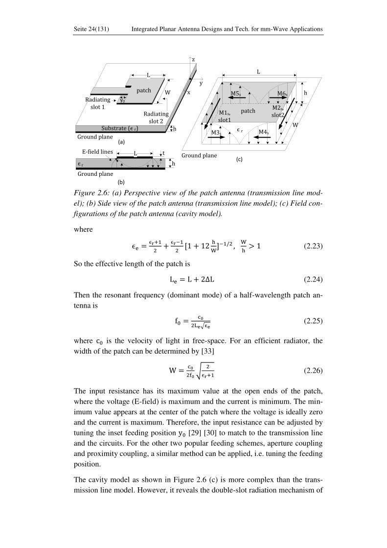
Seite 24(131) Integrated Planar Antenna Designs and Tech. for mm-Wave Applications
L
h
z
y
x
Ground plane
Radiating
slot 1Radiating
slot 2Substrate (ϵ r)
patch
y0
E-field lines L
Ground plane
h
tϵ r
(a)
(b)
M2s,
slot2M1s,
slot1
patch
W
Ground plane(c)
M3s M4s
M5s M6s
ϵ rW
L
h
Figure 2.6: (a) Perspective view of the patch antenna (transmission line mod-
el); (b) Side view of the patch antenna (transmission line model); (c) Field con-
figurations of the patch antenna (cavity model).
where ϵ = ϵ + + ϵ − [ + W]− / , W > (2.23)
So the effective length of the patch is � = � + ∆� (2.24)
Then the resonant frequency (dominant mode) of a half-wavelength patch an-
tenna is f = √ϵ (2.25)
where c is the velocity of light in free-space. For an efficient radiator, the
width of the patch can be determined by [33] W = √ϵ + (2.26)
The input resistance has its maximum value at the open ends of the patch,
where the voltage (E-field) is maximum and the current is minimum. The min-
imum value appears at the center of the patch where the voltage is ideally zero
and the current is maximum. Therefore, the input resistance can be adjusted by
tuning the inset feeding position λ [29] [30] to match to the transmission line
and the circuits. For the other two popular feeding schemes, aperture coupling
and proximity coupling, a similar method can be applied, i.e. tuning the feeding
position.
The cavity model as shown in Figure 2.6 (c) is more complex than the trans-
mission line model. However, it reveals the double-slot radiation mechanism of

2 Basic Considerations on Planar mm-Wave Antenna Development Seite 25(131)
a patch antenna in a clearer way. It models the patch antenna as a dielectric-
loaded cavity with 2 PEC walls (patch and ground plane) and 4 perfectly mag-
netic conducting (PMC) walls (sidewalls). It assumes that the substrate is trun-
cated and does not extend beyond the patch. The sidewalls represent 4 narrow
(h is small) slots. The E-field distribution of the dominant mode [2] of the
patch antenna is illustrated in Figure 2.6 (c). The boundary condition of the
fields at a PMC wall is −n × E = M (2.27a) n × H = J = (2.27b)
where n is the normal unit vector pointing out of each sidewall. From (2.27) we
can see that there are only magnetic surface current density sources on the
slots. The magnetic sources (M and M ) on the radiating slot 1 and 2 have
equal magnitude and phase, and they form a two element slots array which
gives a broadside radiation. The radiation from the sources on the other two
slots cancels each other in the principle planes because of their equal magni-
tudes but opposite phases. The radiation from them in the non-principle planes
is also smaller than that from radiating slot 1 and 2, so they are usually consid-
ered as non-radiating slots. The patch antenna based designs are presented in
chapter 3 by using PCB technology for 60 GHz applications, and in chapter 5
by using polymer above-wafer process for 122 GHz applications.
2.2.3 Vivaldi Antenna
One of the most attractive features of the mm-Wave applications is its large
available bandwidth, e.g. 57–66 GHz in the 60 GHz band in Europe. It requires
wideband integrated antennas, which preferably have constant beamwidth,
gain, and fairly good reflection coefficient over the entire bandwidth. The Vi-
valdi antenna as shown in Figure 2.7 (a) was originally reported in [34]. It is a
member of aperiodic continuously scaled, gradually curved, non-resonant, and
end-fire travelling wave antenna structures. It can be easily implemented on a
thin film substrate by printed circuits technologies [34] [35]. The shape of the
tapered slot is described by an exponential function [34] λ = ±Ae (2.28)
where λ is the half separation of the slot lines, x is the length of the slot, A is a
half of the minimum slot width, and β is the magnification factor which deter-
mines the beamwidth. Different parts of the antenna radiate efficiently at dif-
ferent frequencies, while the size of the radiating parts is constant in wave-
length. Therefore, the Vivaldi antenna has theoretically unlimited bandwidth.
In practice the high and low frequency limit will be determined by the mini-
mum and maximum slot width of W and W , respectively, due to the finite

Seite 26(131) Integrated Planar Antenna Designs and Tech. for mm-Wave Applications
antenna size. The cut-off wavelength is defined as = W . The frequencies
that have longer wavelength will not be radiated efficiently. The gain is propor-
tional to the overall length � of the antenna which is in common with other
travelling wave structures [36].
The bandwidth of the Vivaldi antenna can be limited by its feeding mechanism,
i.e. the transition of planar transmission lines to the slot line. The transition
needs to be sophisticatedly considered and designed together with the antenna
for specific applications [37]–[39]. A derivative of the Vivaldi antenna, which
is named as bunny-ear antenna, was originally introduced in [40], and further
characterized in [41] and [42]. As shown in Figure 2.7 (b) the transition from a
pair of balanced planar transmission lines to the radiating slot is exponentially
tapered to achieve a wideband impedance matching. This structure is inherent-
ly compatible with a differential circuit, which has many advantages over its
single-ended counterpart. A differential bunny-ear antenna design is presented
in chapter 3 for 60 GHz applications.
y
xo
WL
L
ϵr
WH
metal
Tapered
slot
(a) (b)
WHϵr
WL
L
Tapered
transitionmetal
Figure 2.7: (a) The Vivaldi antenna; (b) The bunny-ear antenna.
2.2.4 Antenna Arrays
The planar antennas usually have low gain and efficiency. In many applications
it is desired to have a high gain, a narrow and steerable beam of the antenna to
mitigate the noise and clutter or improve the quality of service even in a non-
line-of-sight radio link. A planar phased array antenna comprises of a certain
number of antenna elements, which are normally identical, with individually
controllable excitation magnitudes and phases in a suitable geometrical ar-
rangement. The radiation from each element will add constructively or destruc-
tively in certain spatial directions that the steerable beams are achieved. The
radiation pattern is the product of a single element factor and an array factor,
assuming no mutual coupling. As the frequency comes to the mm-Wave range,
the size of a planar phased array shrinks so that it becomes possible to be inte-

2 Basic Considerations on Planar mm-Wave Antenna Development Seite 27(131)
grated with the ICs in a module. On the other hand, the complex feeding net-
work and antenna elements are fabricated on the same substrate, which can
lead to considerably undesirable coupling due to the substrate modes and spu-
rious radiation. Large mutual coupling levels among the antenna elements can
degrade sidelobe levels, main beam shape, and possibly cause array blindness
[43]. The spurious radiation from the feeding lines can interfere with the radia-
tion patterns significantly. The development of a phased array antenna is a
complicated task, which includes selection of substrate, determination of an-
tenna elements and its feeding methods, design of a single element, and finally
the design of complete antenna array. Special efforts should be made to design
the feeding networks.
2.3 Substrates
The substrate takes a crucial role in the mm-Wave planar antenna designs. The
permittivity of the substrate is directly related to the electrical dimensions of
the structures in or on it, which decide the resonant frequencies. The permittivi-
ty of the dielectrics generally changes with frequency due to its physical na-
ture, and in practice it is determined experimentally in the interested frequency
bands for the accurate values, although there are theoretical equations, like De-
bye equation [44], to calculate it as a function of frequency for some ideal cas-
es.
As the wavelength decreases in the mm-Wave range, the substrate becomes
electrically thick so that the higher order modes of substrate waves are support-
ed. They propagate in the substrate and dissipate as losses which lower the ra-
diation efficiency of the antenna. In addition, they can be diffracted at the trun-
cated edges of the substrate of finite size. The diffracted fields can interfere
with the main radiation patterns and distort them. The following discussion on
substrates is given in two aspects: the characterization of dielectric properties
and the substrate modes.
2.3.1 Dielectric Characterization
The most important properties of a dielectric substrate in antenna designs are
described by its complex permittivity as
ϵ = ϵ′ − jϵ′′ (2.29)
The imaginary part ϵ′′ accounts for the loss in the dielectric (heat) due to
damping of the vibrating dipole moments, when an alternating electric field is
applied [4]. In practice the complex permittivity is more often expressed by the
relative permittivity ϵ (or dielectric constant), and the loss tangent tan as

Seite 28(131) Integrated Planar Antenna Designs and Tech. for mm-Wave Applications
ϵ = ϵ′ − jtan = ϵ ϵ − jtanδ)
tan = ωϵ′′+σωϵ′ (2.30)
where ω is the angular frequency of the applied field, and σ is the conductivity
of the dielectric which results in conductive loss. The manufacturers of the
substrates usually give the properties only at relatively lower frequencies ( 10
GHz), which is not adequate for mm-Wave designs. A variety of dielectric
characterization techniques have been proposed, and each of them has its own
advantages and limitations.
The method of resonant cavities offers high Q measurement. Closed cavities
can be used for liquid or mold materials, while open resonators have been
proven capable to measure the complex permittivity of very low-loss, thin, and
planar dielectrics in the mm-Wave range [45]–[48]. However, it is complex to
implement them. The printed resonant circuits such as resonant rings [49] or
open stubs, which are easier to implement, can also be used to have a good es-
timation of the permittivity. But it is difficult to measure the loss from the die-
lectric because of the non-negligible loss from the conductors.
Broadband characterization of dielectrics usually involves various transmission
line approaches. They are generally insensitive to very low losses. A wave
propagates along a general non-ideal transmission line will have a complex
propagation constant, which includes the information of the phase velocity and
the attenuation constant. Therefore, the relative permittivity and loss tangent
can be extracted by analyzing the phase and magnitude of the measured reflec-
tion (S , S ) and transmission coefficients (S , S ), respectively. The free-
space can be viewed as a special type of transmission line. In a free-space
method setup [50] [51] a thin planar sample is placed between two antennas,
normally horn antennas, and the S-parameters are measured to extract the die-
lectric properties. This approach is found very useful in the mm-Wave range,
although the experimental setup and the free-space calibration is complex.
Open-ended or filled transmission lines like coaxial lines or rectangular wave-
guides can also be used to characterize the dielectrics [45] [52]–[54]. But it still
needs some efforts to fit the dielectrics to the transmission lines properly. The
planar transmission line approach, either microstrip [55] or coplanar waveguide
(CPW) [56], is probably the simplest way to evaluate the dielectric properties
for the mm-Wave planar antenna applications. They can be fabricated on the
same substrate as the planar antennas by using the same technology. The S-
parameter is measured by microwave probes, and after applying certain de-
embedding techniques the complex propagation constant can be extracted, thus
obtaining the effective permittivity and attenuation constant. Finally, analytical
formulas can be used to calculate the complex permittivity of the substrate.
This method will be employed to characterize the PCB materials in chapter 3.

2 Basic Considerations on Planar mm-Wave Antenna Development Seite 29(131)
2.3.2 Substrate Waves
An antenna operating on a substrate can excite substrate waves, which lower
the radiation efficiency and possibly distort the radiation patterns. The sub-
strate modes in two scenarios in this thesis, a grounded dielectric (surface
waves) and a parallel plate dielectric waveguide (guided waves), are studied in
this section.
A. Surface Waves on a Grounded Dielectric
A typical configuration of a planar antenna is that a radiator is formed on top of
a grounded dielectric substrate. We can understand qualitatively how the an-
tennas radiate and excite surface waves from a ray point of view. In Figure 2.8
a point source (antenna) is located on a dielectric (ϵ ) at (d, , ). It radiates
waves directly into free-space above the dielectric, which are designated as ra-
diated waves. At the same time the source also excites waves (can be many
modes at discontinuities of an antenna) into the dielectric, and they are reflect-
ed by the ground plane to the dielectric-air interface. In this case the Snell’s law for either parallel or perpendicular polarization can be written as
sinθ = √ϵϵ sinθ = √ϵ ϵϵ sinθ = √ϵ sinθ , ϵ > (2.31)
where θ is the incidence angle, and θ is the refraction angle. It can be seen
from (2.31) that if θ increases, the refraction angle θ will increase at a faster
rate. Therefore, when θ reaches the so called critical angle θ , θ will be 90°.
When the incidence angle is smaller than the critical angle (see θ = θ < θ in
Figure 2.8), the waves are partially reflected by the dielectric-air interface and
progressively leaking into the air (leaky waves), thus eventually contributing to
radiation. If the incidence angle θ is equal to or beyond the critical angle θ
(see θ > θ in Figure 2.8), the incident waves will be totally reflected. Then
the waves are trapped inside the dielectric and propagating along as surface
waves, which decay exponentially away from the dielectric surface (x d)
along h. The surface waves spread out in a cylindrical fashion around the
source point, and the amplitude of the fields decay with distance /√δ that
more slowly than space waves ( /δ) [16] [57]. The surface waves are generally
considered as losses since they are trapped in the dielectric of infinite size, and
do not contribute to radiation. However, for the dielectric with finite size the
surface waves can be reflected and diffracted at the truncated edges, thus caus-
ing spurious radiation that probably distorts the main radiation patterns. In ad-
dition, the travelling of the surface waves will introduce coupling between the
antennas or circuits which are fabricated on the same substrate. This effect can
severely degrade the performance of an antenna array and even lead to mal-
function (array blindness).

Seite 30(131) Integrated Planar Antenna Designs and Tech. for mm-Wave Applications
x
z
Radiated waves
Air ϵ0
d
Dielectricϵrϵ0
Leaky waves Edge diffracted
waves
Surface wavesθc
θ1 θc
θ2
h o
Ground plane
θi = θ1
θt
θi = θ2
Figure 2.8: Presentation of a grounded dielectric and various waves.
The surface waves require certain conditions to propagate in a dielectric after
being excited. A grounded dielectric cannot support transverse electromagnetic
(TEM) waves because it is a non-homogeneous media. Transverse magnetic
(TM) and transverse electric (TE) surface waves will be studied. The general
solutions for the TEM, TM, and TE waves are given in the appendix A.
TM Modes
Consider the grounded dielectric as shown in Figure 2.8. The dielectric has a
dielectric constant of ϵ and a thickness of d. We assume the dielectric has in-
finite extent in the λ and μ direction, and the surface waves propagate along
(+μ) with an e− propagation factor and no variation in the y direction
(∂ ∂λ⁄ = ).
The longitudinal electric field E x, λ, μ = e x, λ e− must satisfy the
Helmholtz equation in both the dielectric and air regions: ∂∂ + ∂∂ + ∂∂ + ϵ k e x, λ e− = , foδ x d (2.32a)
∂∂ + ∂∂ + ∂∂ + k e x, λ e− = , foδ d x < ∞ (2.32b)
where k = ω√ϵ is the wave number in free-space. Taking into account ∂ ∂λ⁄ = , (2.32) can be reduced to ∂∂ + ϵ k − e x, λ = , foδ x d (2.33a) ∂∂ + k − e x, λ = , foδ d x < ∞ (2.33b)
The cutoff wavenumbers for the two regions are defined as k = ϵ k − , foδ x d (2.34a) h = − k , foδ d x < ∞ (2.34b)
where the sign on h is chosen in anticipation of an exponentially decaying
along x-axis above the dielectric-air interface [4]. The propagation constant
of a certain surface wave must be the same in both air and dielectric regions to

2 Basic Considerations on Planar mm-Wave Antenna Development Seite 31(131)
achieve phase matching of the tangential fields at the dielectric interface for all
values of μ. The general solutions to (2.33) are e x, λ = Asink x + Bcosk x, foδ x d (2.35a) e x, λ = Ce + De− , foδ d x < ∞ (2.35b)
The boundary conditions are E x, λ, μ = , at x = (2.36a) E x, λ, μ < ∞, as x → ∞ (2.36b) E x, λ, μ continous, at x = d (2.36c) H x, λ, μ continous, at x = d (2.36d)
From appendix A we have H = E = H = . The boundary conditions
(2.36a) and (2.36b) imply that B = and C = in (2.35). Then from the con-
tinuous condition of (2.36c) we have Asink d = De− (2.37)
As indicated in (2.36d) the magnetic field must be also continuous at the inter-
face, from (2.35) and (A.6) in appendix A we have ϵ A cosk d = e− (2.38)
Combine (2.37) and (2.38) to eliminate A and D, then k tank d = ϵ h (2.39)
Eliminating from (2.34) we can get another equation k + h = ϵ − k (2.40)
Given d and k , then k and h can be solved numerically from (2.39) and
(2.40). However, a graphical solution can show the results more visually. Mul-
tiplying both sides of (2.39) and (2.40) by d and d , respectively, we have k d tan(k d = ϵ hd (2.41a) k d + hd = ϵ − k d (2.41b)
(2.41a) and (2.41b) can be plotted on the k d–hd plane as shown in Figure 2.9
for 2 dielectric constants ϵ =3 and ϵ =11.9, which are the values of some often
used PCB materials (e.g. Rogers 3003) for on-board antenna designs and sili-
con for on-chip antenna designs. Each intersection of the curves, which are
constituted by (2.41a) and (2.41b), implies a common solution to both of them.
Only the first quadrant is plotted, because h should be positive real due to the
waves decaying along the x-axis, and a negative k merely changes the sign of

Seite 32(131) Integrated Planar Antenna Designs and Tech. for mm-Wave Applications
2
2 3
3
2
2
3
3
00kcd kcd
hd
hd
(a) ϵr=3 (b) ϵr=11.9
d=0.1 0
d=0.25 0
d=0.5 0
d= 0
d=0.1 0
d=0.25 0
d=0.5 0
(2.41a)(2.41b)
(2.41a)(2.41b)
Figure 2.9: Graphic solutions to (2.41) for TM modes with (a) � =3 and (b) � =11.9.
constant A in (2.35a). (2.41b) is an equation of a circle with a radius of √ϵ − k d. As √ϵ − k d increases, either ϵ or d or both, the circle may
have more intersections with the tangent function curves described by (2.41a),
implying that more TM modes can propagate.
It can be observed that for an ordinary dielectric, which has a finite thickness
and a dielectric constant greater than 1, there is always at least one propagating
TM mode, designated as TM0 mode, which has a zero cutoff frequency. TM0
mode can have some field lines aligned with the field lines of the quasi-TEM
mode of microstrip lines, which are often used to construct feeding structures
of planar antennas on the dielectrics. The fields of the TM0 mode are zero at
zero frequency, so the coupling to the quasi-TEM mode is negligible until a
threshold frequency is reached. Studies have shown that the threshold frequen-
cy can be defined as [58] f = π √ϵ − tan− ϵ (2.42)
For ϵ > , (2.42) reduces to [58] f GHμ = .√ϵ d in cm (2.43)
The higher order modes TMn will start propagating when the radius of the cir-
cle reaches n (Figure 2.9). Therefore, the cutoff frequency of the TMn modes
can be derived as √ϵ − π d = n (2.44a) f = √ϵ − , n = , , , … (2.44b)

2 Basic Considerations on Planar mm-Wave Antenna Development Seite 33(131)
As soon as k and h have been determined, the complete expressions for the
fields can be obtained from (2.34), (2.35), (2.37), and (A.6) in appendix A as E x, λ, μ = {Asink xe− foδ x dAsink de− − e− foδ d x < ∞ (2.45a)
E x, λ, μ = { − Acosk xe− foδ x d− Asink de− − e− foδ d x < ∞ (2.45b)
H x, λ, μ = { − ωϵ ϵ Acosk xe− foδ x d− ωϵ Asink de− − e− foδ d x < ∞ (2.45c)
TE Modes
The TE modes can be solved in a similar procedure as that for TM modes. The
longitudinal magnetic field must satisfy the wave equations ∂∂ + k h x, λ = , foδ x d (2.46a) ∂∂ − h h x, λ = , foδ d x < ∞ (2.46b)
After applying the certain boundary conditions to the general solutions of the
fields in two regions, two equations can be achieved as − k d cot(k d = hd (2.47a) k d + hd = ϵ − k d (2.47b)
where k and h can be solved by either numerical or graphical approach. The
cutoff frequency of TEn modes can be found as f = −√ϵ − , n = , , , … (2.48)
For most of antenna designs, the higher order surface wave modes should be
avoided to maintain high radiation efficiency within the bandwidth of interest.
The selection of substrates, i.e. the dielectric constant ϵ and the thickness d,
is important to minimize the number of propagating surface wave modes. Fig-
ure 2.10 shows a plot of the cutoff frequencies (below them certain surface
wave modes will become evanescent modes) of some foremost surface wave
modes as a function of the substrate thickness d for two common dielectric
constants ϵ =3 and ϵ =11.9, which give references for a large variety of low
and high permittivity substrates for planar mm-Wave antenna designs. The
threshold frequency f defined in (2.42) and (2.43), below which there is little
coupling between the TM0 mode with zero cutoff frequency and the Quasi-
TEM mode of microstrip lines, is also plotted. The propagation constant of
the higher order surface wave mode is small when its cutoff frequency is just

Seite 34(131) Integrated Planar Antenna Designs and Tech. for mm-Wave Applications
(a) ϵr=3
d (µm)200 400 600 800 1000 200 400 600 800 10000
50
100
150
200
250
300
50
100
150
200
250
300
0d (µm)
(b) ϵr=11.9
f c (
GH
z)
f c (
GH
z)
TE1
TM1
TE2
TM2
TE1
TM1
TE2
TM2
TEn
TMn
fcTM0=0
fT
fT
fT
TEn
TMn
fcTM0=0fT
Figure 2.10: Plotting of cutoff frequencies of TMn and TEn surface wave
modes as well as the threshold frequency as a function of dielectric thick-
ness. (a) � =3; (b) � =11.9.
reached ( = k at the cutoff frequency for certain mode). As frequency in-
creases will be more close to or even exceed the guided wave propagation
constant of the antenna, then the modes coupling and loss become more signif-
icant.
B. Parallel Plate Guided Waves
It is quite normal that there is a metal layer also on top of the dielectrics, espe-
cially for the on-chip designs because there is requirement on the minimum
global metal density for each metal layer in the back-end-of-line (BEOL) pro-
cess, and the chip is usually seated on a ground plane of a package. In this case
a parallel plate waveguide is formed at least locally. The geometry of such a
waveguide is shown in Figure 2.11. We assume the width of the waveguide in λ direction is very large compared with the thickness d so that fringing fields
and any y variations can be ignored, and the guided waves propagate in the +μ
direction with an e− propagation factor. Since the media is homogeneous, it
can support TEM mode besides TM and TE modes. The analysis of the modes
is analogous to that for a grounded dielectric, so the detailed analysis will not
be repeated here. The cutoff frequency for the TEM mode is zero, and the cut-
off frequency for TMn and TEn modes is identical as f = √ ϵ ϵ , n = , , … (2.49)
x
z
d
Top metal plate
Bottom metal plate
Dielectric ϵrϵ0 o
Figure 2.11: Geometry of a parallel plate waveguide.

2 Basic Considerations on Planar mm-Wave Antenna Development Seite 35(131)
(a) ϵr=3
d (µm)200 400 600 800 1000 200 400 600 800 10000
50
100
150
200
250
300
50
100
150
200
250
300
0d (µm)
(b) ϵr=11.9
f c (
GH
z)
f c (
GH
z)
TM1,TE1
TM2,TE2
fcTEM=0
TM1,TE1
TM2,TE2
TM3,TE3
TM4,TE4
fcTEM=0
Figure 2.12: Plotting of cutoff frequencies of TMn and TEn modes in a paral-
lel plate waveguide as a function of d. (a) � =3; (b) � =11.9.
There is no TE0 mode, and the TM0 is actually identical to the TEM mode. The
cutoff frequency f of the TMn and TEn modes is plotted as a function of the
dielectric thickness d in Figure 2.12 for ϵ =3 and ϵ =11.9, respectively. It can
be observed that the cutoff frequencies for the higher order modes are higher
than those of the surface waves in a grounded dielectric slab with the same die-
lectric constant and thickness (Figure 2.10).
2.4 Antenna Measurement
At mm-Wave frequencies the planar antenna measurements are very challeng-
ing. Conventionally, the antenna under test is connected to the measurement
setup by a coaxial cable or a waveguide connector. However, the feature sizes
of these types of connectors are too large for the printed planar mm-Wave an-
tennas, especially for the on-chip antennas. A probe based antenna measure-
ment takes the advantages of measuring exactly at the reference plane of inter-
est, and avoiding the effort of mounting connectors, which is a very difficult
task or even not possible. On the other hand, there are also challenges. A spe-
cial calibration procedure has to be conducted to the measurement setup, which
is vital to achieve an accurate measurement. As many other measurements us-
ing a microwave probe, the measurement is sensitive to vibration so that the
AUT cannot be rotated, and has to be well fixed on a sample holder. Since the
shielding of a microwave probe is worse than that of a conventional connector
for antenna measurement, the spurious radiation and reflection from the probe
will limit the dynamic range.
The radiation performance of the antennas in this work was measured at the
Karlsruhe Institute of Technology (KIT) by a microwave probe based meas-
urement setup as shown in Figure 2.13, which is described in detail in [1] and
[59]. The mechanical assembly of the system as illustrated in Figure 2.13 (a)
contains two arms and two rotary stages, which are consistent with the azimuth
and elevation angles, to rotate the receive horn antenna around the AUT to

Seite 36(131) Integrated Planar Antenna Designs and Tech. for mm-Wave Applications
measure nearly the 3-D radiation patterns or three sectional planes in a far-field
distance of 60 cm. However, the existence of the table will limit the measure-
ment range to about 270° in horizontal plane and 255° in one vertical plane.
The receive horn antenna can be rotated 90° to enable the measurement of two
polarizations. The AUT, specifically the part containing the probing pads is
well fixed on a sample holder that is made of dielectric foam (ϵ < . , tan <. , resembling air in terms of electric properties. In this way the radiating
part of the AUT can be positioned in the air, and thus achieving measurement
in a quasi-in-air condition, as shown in Figure 2.13(b). For the measurement in
different frequency bands the frequency modules (RF sources and harmonic
mixers) as well the RF probes are interchanged.
The principle of the calibration procedure is explained in detail in Chapter 17
of [60]. To sum up, it requires three steps. First, the transmit path of the system
is calibrated to the reference plane at the input port 1 of the reference horn an-
tenna and the probe as shown in Figure 2.14. In the second step a reference
horn antenna with well-known gain G is attached to the system to calibrate
the free-space loss and the system losses as shown in Figure 2.14 (a). From the
measured S , we can get G = | , | (2.50)
with G representing all system losses (including free-space loss) and the
gain of the receive horn antenna. The third step is the calibration of the probe
as shown in Figure 2.14 (b), which moves the reference plane to the probe tips
to measure the complex input impedance of the device. The short-open-load
(SOL) method is employed to make the 1-port (only port1) calibration by using
(a)
(b)
(c)
Coaxial cable
(b)
(c)AUT Waveguide probe
D-band module
AUTProbe tips
Figure 2.13: Probed based measurement setup [1][59]: (a) mechanical assem-
bly, (b) coaxial cable probe and AUT contact, (c) D-band (110–170 GHz)
transmit/receive module, waveguide probe, and the AUT.

2 Basic Considerations on Planar mm-Wave Antenna Development Seite 37(131)
Reference
plane
Reference horn Receive horn
Receive horn
Receive horn
Port 1 Port 2
Port 1
Port 1
Port 2
Port 2
Calibration
substrate
AUT
Reference plane
at probe tipsProbe
Probe
(a)
(b)
(c)
Gref
Figure 2.14: Calibration procedure for a probe based mm-Wave antenna
measurement setup: (a) gain calibration, (b) probe calibration, (c) AUT meas-
urement.
Reference plane
at port 1
Reference plane
at probe tips
a0
b0
e10
e01
e00 e11
a1
b1
Error adapter
ΓM ΓA AUT
Figure 2.15: 1-port SOL calibration error model.
a standard calibration substrate. The 1-port SOL error model is shown in Fig-
ure 2.15. The relationship between the measured reflection coefficient Γ with
error and the actual reflection coefficient ΓA at the device itself at the reference
plane can be written as [60] Γ = = e + ΓA− ΓA (2.51a) ΓA = ΓM−ΓM− + (2.51b) Γ , , Γ , , and Γ , can be obtained by measuring the short, open, and
load calibration standards on the calibration substrate, while ΓA, , ΓA, ,
Seite 38(131) Integrated Planar Antenna Designs and Tech. for mm-Wave Applications
and ΓA, are the known calibration standard values. They yield three equa-
tions with three unknown error factors (e , e , and e e ) so that the un-
known error factors can be determined by calculation. Knowing the error fac-
tors, ΓA can be calculated from Γ in the antenna measurements. Assuming the
error adapter is perfectly reciprocal e = e , the gain of the probe can be
expressed as G = e e (2.52)
Finally the antenna measurement can be implemented as shown in Figure 2.14
(c), and the proper gain GA of the AUT can be calculated from the directly
measured result S , as GA = | ,M|m∙ (2.53)
2.5 Preliminary Considerations on mm-Wave Antenna De-
sign and Integration
The integration of antenna into an mm-Wave system takes a vital role, and is
very challenging. Many methods and technologies for mm-Wave packaging
and antenna integration have been developed, which are discussed below.
2.5.1 Chip-on-Board with Integrated PCB Antenna
Figure 2.16 (a) and (b) illustrate the concept of a RFIC, which is directly at-
tached on a PCB, incorporating with an integrated PCB antenna by using mm-
Wave interconnect technologies, bond-wire and flip-chip, respectively. As
shown in Figure 2.16 (a) the chip is glued on the ground plane of the PCB,
which also acts as a large heat sink for the chip. The RF I/O of the chip is in-
terconnected to the antenna by wire-bonding. The wire-bonding is a mature,
thermal expansion insensitive, and high yield process that supports a well-
established low-cost infrastructure with high reliability. Unfortunately, the
electrically long loop of the bond-wires will introduce considerable parasitic
effects (about 1 nH/mm of inductance as a rule of thumb) so that they exhibit
low-pass frequency characteristics in the mm-Wave range. The bond-wire with
short length is difficult to produce, and the repeatability is a serious issue. Con-
sequently, special compensation designs and process control for bond-wires
have to be applied in order to achieve acceptable performance within the
bandwidth of interest [26] [61] which increase the assembly complexity, and
the cost. As frequencies increase to above 100 GHz or even above 200 GHz the
compensation for bond-wires becomes much more difficult (requires very pre-
cise fabrication technology and process control), if it is not impossible.

2 Basic Considerations on Planar mm-Wave Antenna Development Seite 39(131)
IC Antenna
PCB
IC Antenna
PCB
IC
Antenna
PCB
(a) Bond-wire (b) Flip-chip (c) Bond-wire and Flip-chip
Frame
Figure 2.16: Chip-on-board with integrated PCB antenna by using: (a) bond-
wire solution, (b) flip-chip solution, (c) bond-wire and flip-chip solution.
Figure 2.16 (b) shows a flip-chip solution with bump interconnects, which of-
fers a very short transition between the chip and the PCB antenna. Therefore,
the parasitic effects associated with a bump itself are significantly smaller than
that of a bond-wire, showing a wide application potential at mm-Wave fre-
quencies above 100 GHz and even higher up to 170 GHz with a compensation
scheme [62] [63]. Moreover, the bumps can be placed on the entire die area
that it enables a much higher I/O count compared with that of the bond-wire
solution, which can only use the periphery of the chip. The density of the
bumps will be constrained by the normal PCB manufacturing technology
whose minimum line width and spacing are limited to about 100 µm. The
flipped-over chip mounting onto an underlying PCB gives other types of para-
sitic problems. They can result in considerable deterioration in performance of
the overall packaged mm-Wave system if special cares are not taken in the de-
signs. Obviously, the electrical parameters of various circuit elements on the
chip surface, e.g. inductors, couplers or any structures made of transmission
lines, will be influenced by the proximity effects to the PCB, especially when a
metallization is present on the PCB below the chip [64], thus causing chip de-
tuning. The different coefficient of thermal expansion (CTE) of the chip and
the PCB material can cause a strain on the flip-chip joints that arises reliability
issues, so an underfill process (e.g. a thermal compression technology) is often
required to absorb the stress. The price is that the underfill materials will prob-
ably introduce additional detuning effects as well as more losses. Another
problem has to be considered is that unlike the case of a chip directly seating
on a large heat sink (metal ground plane) on a PCB, the upside-down configu-
ration of the chip has limited heat dissipation capability that could result in se-
vere performance degradation of the RF circuits.
A combination of the bond-wire and flip-chip technologies can take the ad-
vantages of both technologies as shown in Figure 2.16 (c). The low frequency
I/O and DC supplies of the chip, which are not sensitive to the parasitics, can
be interconnected to the PCB by wire-bonding. The antenna and the RF I/O of
the chip, which are operating at the highest frequencies of the system, are in-
terconnected by flip-chip bumps. The effects of the supporter of the antenna
must be taken into account in the design. In [65] a covar metal frame (rectangle

Seite 40(131) Integrated Planar Antenna Designs and Tech. for mm-Wave Applications
ring type) is used to mechanically support the antenna, and the metal frame to-
gether with the metallic base of the board form a metal cavity which provides a
well-controlled EM environment, making the antenna less sensitive to the sur-
rounding package and PCB-level metal as well as dielectric structures. Another
advantage of this hybrid approach is that an optimal substrate preferably with
low dielectric constant and thicker thickness, which are usually contradictory
to the requirements of other on-board RF passive circuits, can be used for the
antenna since they are not implemented on the same substrate. Apparently, the
packaging and assembly process of the hybrid approach is more complex than
that of a bond-wire or flip-chip solution, resulting in a higher cost.
The chip-on-board (COB) with integrated PCB antenna is a very cost-effective
solution since there are a wide range of low-cost and high-quality RF substrates
available in the market, and the PCB technologies are quite well-established.
The parasitic effects introduced by the chip-antenna interconnect technologies
of wire-bonding or flip-chip can be compensated up to certain frequencies on
the board side in a cost-effective fashion. However, the resolution (e.g. mini-
mum line width and spacing are about 100 µm) and accuracy of normal PCB
technologies limit its applications within the lower band of mm-Wave frequen-
cies. In addition, this method requires mm-Wave expertise in the PCB design
and additional molding process (e.g. glob top [65]) to protect the chip and the
interconnects from mechanical damage and contamination. Nevertheless, it can
be expected that the COB with integrated PCB antenna solution gives better
performance than other packaging methods because of fewer signal transfer
stages (the I/O of the chip is interconnected to the PCB directly), flexibility in
on-board antenna design, and larger possible heat sink. All these characteristics
make this approach very commonly used for mm-Wave system demonstrators
to evaluate the system performance. The designs for 60 GHz applications based
on this method will be demonstrated in chapter 3.
2.5.2 Antenna Integrated In-Package and Antenna Integrated On-
Chip
For mass products it is highly desirable to have an mm-Wave system with inte-
grated antenna in a package. In the mm-Wave range the size of the antenna de-
creases into millimeter range, so it is feasible to integrate it into a small pack-
age or even on-chip. In this case the package confines all high frequency
interconnects inside itself so that only the low frequencies and DC supplies are
transferred between the package and the next level platform, which requires
significantly less efforts and little high frequency expertise. Therefore, the sur-
face mount technology (SMT) can be used to mount the packages in the same
way as other SMT components directly onto the surface of a low-cost PCB
mother board, enabling mass products.

2 Basic Considerations on Planar mm-Wave Antenna Development Seite 41(131)
There are several packaging and antenna integration technologies available for
mm-Wave applications, such as low temperature co-fired ceramic (LTCC) [66]
[67] packages, silicon based packages [68] [69], land-grid-array (LGA) pack-
ages [70], plastic quad flat no-lead (QFN) packages [71], etc. Among them the
plastic QFN package is the simplest and probably the cheapest. The following
discussion on antenna integration in-package is based on a QFN package as an
example, but many conclusions can also be applied on other package platforms
(e.g. parasitic effects of wire-bonding and flip-chip technologies).
Figure 2.17 shows an example of very low-cost plastic air cavity QFN package
(10 mm × 10 mm × 0.635 mm) with a typical pin pitch of 0.5 mm from the
market [72], which is compatible with SMT process. There are more standard
and customized sizes available to accommodate chips and antennas with differ-
ent sizes. The larger center metal pad can act as a good heat sink for the chip to
transfer the heat from the package to the outside PCB, and it can also serve as a
reflector for the in-package antenna to enhance the broadside radiation. This
package can be encapsulated by filling of molding compound or closed by a
flat lid or a dome. The molding compound is usually very lossy at mm-Wave
frequencies, and can introduce uncertainties to the antenna’s behavior [65]. A
lid can be made of various dielectric materials (e.g. plastic, glass, ceramic alu-
mina, etc.) with standard or customized sizes and thicknesses. It has been
demonstrated in [71] that a lid with a thickness of half-wavelength (d = . )
has little influence on the radiation performance of the in-package antenna,
thus being a recommended solution. The reason is that the reflections of the ra-
diated wave at the air-lid (dielectric) interface can be analyzed by a transmis-
sion line method [73]. That is when the radiated wave incident at the air-lid in-
terface normally or the incident angle is small the flat lid sheet acts as a half-
wavelength transmission line with wave impedance Z , which transforms the
free-space wave impedance Z outside the package onto itself inside the pack-
age, thus theoretically no reflections.
(a) (b) (c)
Figure 2.17: A plastic air cavity quad flat no-lead (QFN) package (10 mm ×
10 mm × 0.635 mm) with a pin pitch of 0.5 mm [72]: (a) perspective view, (b)
top view, (c) bottom view.

Seite 42(131) Integrated Planar Antenna Designs and Tech. for mm-Wave Applications
IC Antenna
Lid Lid
Antenna
IC
Lid
AntennaIC
(a) (b)
(c)
Lid
Ant.
IC
(d) Figure 2.18: Antenna integration concepts based on a QFN package: (a) an-
tenna on dielectric, (b) antenna on superstrate or dielectric resonator antenna,
(c) antenna on-chip with localized backside etching process, (d) antenna fabri-
cated in an above-wafer process.
Figure 2.18 shows some examples of possible antenna integration concepts
based on a QFN package. In Figure 2.18 (a) an antenna is fabricated on a thin
dielectric, and glued on the center pad of the package with epoxy adhesive. The
antenna and the chip are interconnected by wire-bonding, but in fact any chip-
on-board and PCB antenna integration methods shown in Figure 2.16 can be
applied in this package. Since a suitable high-quality dielectric and advanced
fabrication technology can be used for the antenna, and it is flexible to config-
ure the antenna like making a metallized air cavity on the center pad of the
QFN package below the antenna [71], the antenna on dielectric method can
give very good radiation performance (e.g. an antenna radiation efficiency of
75% including the bond-wire loss was achieved for 122 GHz applications in
[71]). The low frequency I/Os and DC supplies of the chip are interconnected
to the inner pins of the package by wire-bonding, and transferred to the outer
pins. For a flip-chip approach the chip can be attached to the dielectric of the
antenna (or an interposer layer), and the low frequency I/Os as well as the DC
supplies are spread out by transmission lines on the dielectric, and then wire-
bonded to the pins of the package. Obviously, all the RF packaging problems
related to bond-wire or flip-chip technologies also exist here.
To avoid using the complex RF interconnect processes, the antenna has to be
implemented on-chip as shown in Figure 2.18 (b)–(d). In these cases only the
low frequency signals and DC supplies are required to be transferred between
the chip and package by simple bond-wires, thus greatly reducing the difficulty

2 Basic Considerations on Planar mm-Wave Antenna Development Seite 43(131)
in packaging. The challenges come from the design of on-chip antennas. The
BEOL process of silicon technologies usually offer several metal layers buried
in an insulator (silicon dioxide or its variations) on a chip, which can be used to
design antennas. However, it is well-known that on low-resistivity silicon an-
tennas have very low radiation efficiency (<15%) due to the high losses and
substrate wave effects of the silicon substrate used in CMOS or BiCMOS tech-
nologies. In addition, the insulator layer is too thin (~15 µm) to make a ground
shielded (from lossy silicon) antenna with acceptable radiation efficiency
(~10%) [74]. Extensive study and research have been conducted to improve
the performance of the on-chip antennas. The details will be discussed in chap-
ter 4 and chapter 5, while some concepts are described here.
Figure 2.18 (b) shows the concept of superstrate antennas or dielectric resona-
tor antennas (DRA) glued on top of the chip, which are excited by on-chip
transmission lines or on-chip antennas through electromagnetic coupling. The
radiation efficiency of the antennas was improved to 40–60% as reported in
[75]–[77]. This method requires relatively precise alignment and gluing pro-
cess to place the superstrate or dielectric antenna on the right position of the
chip, which adds cost to the antenna-chip assembly. The antenna is vertically
positioned on the chip, so it does not occupy the chip or package area, enabling
a more compact chip size.
In Figure 2.18 (c) an antenna is fabricated by the BEOL process within the
chip, and it can be directly integrated with the active circuits by on-chip inter-
connects like microstrip transmission lines or CPW lines. The on-chip inter-
connects have much higher fabrication precision, bandwidth and reliability
with little parasitic effects than any off-chip RF interconnects so that they can
work at the higher band of mm-Wave and even up to submillimeter-wave re-
gion. The radiation efficiency of the on-chip antenna is improved by selectively
removing the lossy silicon in critical areas by applying an LBE process. The
LBE process is part of standard through silicon vias (TSVs) technology, and is
available in a variety of commercial semiconductor technologies as well as all
of IHP’s SiGe BiCMOS technologies. This process is based on deep reactive
ion etching (DRIE) technology, which enables very high aspect ratio, thus al-
lowing the etched areas with arbitrary shapes in the close vicinity of the active
devices. The packaging and assembly procedure for this concept is extremely
simple, but a considerably larger chip area, which is expensive for low volume
production, is needed since no active devices can be placed under the antenna
or in the etched areas. Therefore, the on-chip antenna with LBE process is
more suitable for higher frequency applications, specifically above 100 GHz
which leads to a smaller form factor for the antennas. There is compromise be-
tween the antenna performance and mechanical stability. It is desired to have a
larger silicon etched area to enhance the radiation efficiency and bandwidth,

Seite 44(131) Integrated Planar Antenna Designs and Tech. for mm-Wave Applications
but the mechanical stability will be reduced in this way since the very thin
membrane (silicon dioxide) is fragile without the support of silicon. In chapter
4 several on-chip antenna designs with LBE process as well as fully integrated
mm-Wave transceivers are presented, targeting higher performance, better me-
chanical stability, and more compact size.
Figure 2.18 (d) demonstrates another approach to integrate an antenna onto an
IC with improved radiation efficiency by applying wafer-level integration
technology. Several polymer layers as well as metal layers are deposited on the
silicon wafer as a post-wafer process. BCB is a widely used polymer for mm-
Wave applications in the thin-film multilayer multichip module with deposited
interconnects (MCM-D) technology due to its low losses, lower mechanical
stress, and better planarization [78]–[80]. The metal layers in the BCB and in
the BEOL process of the silicon technology can be interconnected by vias with
extremely high precision, small feature size, low parasitic effects, and low-loss.
The antennas are realized in the thick copper layers in the BCB with ground
shielding, which shields the antennas from the lossy silicon. In this way the ra-
diation efficiency of the antennas is considerably higher than that of antennas
realized on ordinary low-resistivity silicon. As the antenna can be placed on
top of the chip, it does not increase much of the chip size. However, currently
the total thickness of the deposited BCB is usually within several tens of mi-
crometers, which limits the antenna bandwidth and further improvement of ef-
ficiency. Antenna designs based on this method for 122 GHz applications are
presented in chapter 5.
2.6 Design Flow and Methodology
A successful design of integrated mm-Wave antenna is a systematic work. A
design flow and methodology is proposed by condensing the design experience
from this thesis work into a methodology as shown Figure 2.19. The principle
of the design methodology is that from simpler structures to more complex
structures, and from cheaper (computer simulation based) task to more expen-
sive task (e.g. interconnects characterization, dielectric characterization, proto-
type manufacture, etc.). In this way we expect to save the development time
and cost by minimizing complete re-design cycles and prototype hardware fab-
rications.
First, design specifications have to be defined, which can be divided into two
categories: the applications of the design and the technical requirements of the
design. The design applications will determine, to large extent, which packag-
ing and antenna integration method is preferred to use. For instance the chip-
on-board with integrated PCB antenna as illustrated in Figure 2.16 is a suitable

2 Basic Considerations on Planar mm-Wave Antenna Development Seite 45(131)
Define design specifications
Decide packaging and antenna integration method
Preliminarily design by 3-D EM simulation
Can design specifications be fullfilled?
Thoroughly design by 3-D EM simulation
Results satisfactory?
Design finished
Consider other
approaches
Identify the
problems
Yes
Yes
No
No
Packaging and substrate materials characterization
Prototype manufacture and measurement
Can design specifications be fullfilled?No
Yes
Figure 2.19: Integrated mm-Wave antenna design flow.
approach for 60 GHz system demonstrator applications in the preliminary de-
velopment phase due to its high performance, ease of realization, and low-cost
for in-house system evaluation. In contrast, if the design targets mass products
a compact and low-cost mm-Wave system in-package as shown in Figure 2.18
is more desired. When the application is above 200 GHz an antenna on-chip
solution is the most attractive. The technical requirements are defined from a
system point of view. It usually includes the radiation direction, operation
bandwidth, antenna gain, beamwidth, etc., which have been introduced in sec-
tion 2.1.
As soon as the design specifications have been fixed, the packaging and anten-
na integration method has to be determined with comprehensively considering
the discussions in section 2.5. And then, preliminary design can be started. The
substrate waves were theoretically studied in section 2.3.2, offering references
for selecting the appropriate substrates for the planar antenna designs. Analyti-
cal closed form solutions are only valid for simple antenna structures operating
in simplified environment as discussed in section 2.2, although they do offer
insight into the principle of the antenna operation and the direction for optimi-
zation. In practice the planar antenna and its operating environment are much
more complex so that numerical approaches are indispensable. Three dimen-
sional full-wave electromagnetic (3-D EM) simulators of ANSYS HFSS fre-
quency domain solver based on the finite element method (FEM) [81], and

Seite 46(131) Integrated Planar Antenna Designs and Tech. for mm-Wave Applications
CST microwave studio transient solver based on the finite integration tech-
nique (FIT) [82] are employed in the designs. Both simulators can give accu-
rate prediction of S-parameter and near/far-field results, which have been prov-
en in many designs world widely. The preliminary design is the conceptual
verification and performance evaluation of the selected packaging and antenna
integration method. In this procedure some structures or factors with less influ-
ence over the performance can be simplified or even excluded in the simulated
model to shorten the simulation time, thus enabling more simulations to study
more possible structures.
After implementing extensive simulations based on the selected method we can
have a general idea of whether the design specifications can be fulfilled or not.
If not, we have to re-consider other packaging and antenna integration meth-
ods. (For example, if we found it too difficult to compensate the bond-wire
with acceptable performance in the operation band, we have to consider the
flip-chip or antenna on-chip solutions.) If yes, we proceed with the design into
a more thorough way. The materials for packaging and dielectrics for antenna
are characterized in the frequency band of interest by applying a suitable meth-
od (reviewed in section 2.3.1) when there are no reliable dielectric property da-
ta from the manufacturers or literature. The packaging interconnects are also
characterized in terms of their electrical performance, possible fabrication tol-
erance, reliability, repeatability, etc. Knowing all necessary information thor-
ough design can be conducted. In the simulations all structures including the
antennas, dielectrics, interconnects, and anything could have influence over the
performance are 3-dimensionally modeled as their physical dimensions with
the correct material properties. After optimizing the design, if the results can
fulfill the design specifications we can proceed to manufacture prototypes.
Otherwise, re-consider the packaging and integration method. The measure-
ment plan should be included in the design procedure to guarantee a testable
prototype, and the influence of the measurement structures (e.g. probing pads)
can be de-embedded out from the final results. The antenna measurement setup
and its calibration procedure were introduced in section 2.4. After the meas-
urements we should consider if the results are satisfactory because they can de-
viate from the design due to manufacture tolerance or any other un-considered
factors which make the prototype different from the model in simulations. If
the results are not acceptable we have to identify the problems first, and then
adjust the simulation accordingly which calls for a re-design cycle.
2.7 Conclusions
This chapter introduced the most important antenna parameters with the em-
phasis on their effects in mm-Wave systems. They must be thoroughly consid-
ered and balanced to meet the design specifications for a certain application.

2 Basic Considerations on Planar mm-Wave Antenna Development Seite 47(131)
Some planar antenna models were theoretically studied, which offered insight
into the operation principle of the presented antennas in this thesis as well as
the directions for the antenna optimization. The substrate takes an essential role
in planar antenna designs. A variety of dielectric characterization techniques
were reviewed, and the excitation and propagation of substrate waves were in-
vestigated. The probe based antenna measurement setup and its special calibra-
tion procedure were depicted. The state-of-the-art antenna integration and
packaging methods were extensively reviewed and discussed regarding their
advantages and limitations. By considering all the aforementioned factors and
condensing the design experience in this thesis work into a methodology a de-
sign flow and methodology was proposed in the end of the this chapter.
References
[1] S. Beer, and T. Zwick, “Probe based radiation pattern measurements for highly integrated millimeter-wave antennas,” Antennas and Propagation,
2010 Proceedings of the Fourth European Conference on, pp. 1-5, Apr.
2010.
[2] C. A. Blanis, Antenna Theory: Analysis and Design, 3rd edition, John
Wiley & Sons, New York, 2005.
[3] Shamim, L. Roy, N. Fong, and N. G. Tarr, “24 GHz on-chip antennas and
balun on bulk Si for air transmission,” Antennas and Propagation, IEEE
Transactions on, vol. 56 , no. 2, pp. 303-311, Feb. 2008.
[4] D. Pozar, Microwave Engineering, 4th edition, John Wiley & Sons, New
York, 2011.
[5] J. D. Kraus, Antennas, McGraw-Hill, New York, 1988.
[6] C. –T. Tai, and C. S. Pereira, “An approximate formula for calculating the directivity of an antenna,” Antennas and Propagation, IEEE Transactions
on, vol. AP-24, no. 2, pp. 235-236, Mar. 1976.
[7] R. S. Elliott, “Beamwidth with directivity of large scanning arrays,” The
Microwave Journal, pp. 74-82, Jan. 1964.
[8] S. Voinigescu, High-frequency integrated circuits, Cambridge University
Press, Cambridge, 2013.
[9] P. Herrero, and J. Schoebel, “Planar antennas and beamforming devices
for a multi gigabit 60 GHz demonstrator with quality of service,” Anten-
nas and Propagation, 2010 Proceedings of the Fourth European Confer-
ence on, pp. 1-5, Apr. 2010.
[10] A. Valdes-Garcia et al., “A SiGe BiCMOS 16-element phased-array
transmitter for 60GHz communications,” ISSCC, 2010 IEEE Internation-
al, pp. 218-219, Feb. 2010.

Seite 48(131) Integrated Planar Antenna Designs and Tech. for mm-Wave Applications
[11] S. Emami et al., “A 60GHz CMOS phased-array transceiver pair for mul-
ti-Gb/s wireless communications,” ISSCC, 2011 IEEE International, pp.
164-166, Feb. 2011.
[12] S. Yoshida et al., “A 60-GHz band planar dipole array antenna using 3-D
SiP structure in small wireless terminals for beamforming applications,” Antennas and Propagation, IEEE Transactions on, vol. 61, no. 7, pp.
3502-3510, July 2013.
[13] G. H. Brown, and O. M. Woodward, Jr., “Experimentally determined im-
pedance characteristics of cylindrical antennas,” Proceedings of the IRE,
vol. 33, no. 4, pp. 257-262, Apr. 1945.
[14] G. A. Thiele, E. P. Ekelman Jr., and L. W. Henderson, “On the accuracy of the transmission line model for folded dipoles,” Antennas and Propa-
gation, IEEE Transactions on, vol. 28, no. 5, pp. 700-703, Sep. 1980.
[15] R. W. Lampe, “Design formulas for an asymmetrical coplanar strip folded dipole,” Antennas and Propagation, IEEE Transactions on, vol. 33, no. 9,
pp. 1028-1031, Sep. 1985.
[16] J. F. Zücher, and F. E. Gardiol, Broadband patch antennas, Artech
House, MA, 1995.
[17] R. Wang, Y. Sun, M. Kaynak, J. Borngräber, B. Göttel, S. Beer, and J. C.
Scheytt, “122 GHz patch antenna designs by using BCB above SiGe BiCMOS wafer process for system-on-chip applications,” 2013 IEEE In-
ternational Symposium on Personal, Indoor and Mobile Radio Communi-
cations, London, pp. 1392-1396, Sep. 2013.
[18] A. S. Emhemmed, I. McGregor, and K. Elgaid, “200GHz broadband proximity coupled patch antenna,” Ultra-Wideband 2009, IEEE Interna-
tional Conference on, pp. 404-407, Vancouver, Sep. 2009.
[19] M. Himdi, O. Lafond, S. Laignier, and J. P. Daniel, “Extension of cavity method to analyse aperture coupled microstrip patch antenna with thick
ground plane,” Electronics Letters, vol. 34, no. 16, pp. 1534-1536, Aug.
1998.
[20] K. –L. Wong, and W. – H. Hsu, “A broad-band rectangular patch antenna
with a pair of wide slits,” Antennas and Propagation, IEEE Transactions
on, vol. 49, no. 9, pp. 1345-1347, Sep. 2001.
[21] J. Huang, P. Yang, W. C. Chew, and T. Ye, “A compact broadband patch antenna for UHF RFID tags,” 2009 Asia Pacific Microwave Conference,
pp. 1044-1047, Singapore, Dec. 2009.
[22] G. Rafi, and L. Shafai, “Broadband microstrip patch antenna with V-slot,” Microwaves, Antennas and Propagation, IEE Proceedings, vol. 151, no.
5, pp. 435-440, Oct. 2004.
[23] J. –Y. Sze, and K. –L. Wong, “Broadband rectangular microstrip antenna with pair of toothbrush-shaped slots,” Electronics Letters, vol. 34, no. 23,
pp. 2186-2187, Nov. 1998.

2 Basic Considerations on Planar mm-Wave Antenna Development Seite 49(131)
[24] C. K. Aanandan, and K. G. Nair, “Compact broadband microstrip anten-
na,” Electronics Letters, vol. 22, no. 20, pp. 1064-1065, Sep. 1986.
[25] G. Kumar, and K. C. Gupta, “Directly coupled multiple resonator wide-
band microstrip antennas,” Antennas and Propagation, IEEE Transac-
tions on, vol. 33, no. 6, pp. 588-593, Jun. 1985.
[26] R. Wang, Y. Sun, C. Wipf, and J. C. Scheytt, “ An on-board differential
patch antenna and interconnects design for 60 GHz applications,” 2011
IEEE International Conference on Microwaves, Communications, Anten-
nas and Electronics System, pp. 1-5, Tel Aviv, Nov. 2011.
[27] A. Lamminen, and J. Saily, “Wideband stacked patch antenna array on LTCC for W-band,” Antennas and Propagation, Proceedings of the 5th
European Conference on, pp. 2962-2966, Rome, Apr. 2011.
[28] K. Li, C. H. Cheng, K. F. Tong, and T. Matsui, “Broadband stacked co-
planar patch antennas,” 2001 31st European Microwave Conference, pp.
1-4, London, Sep. 2001.
[29] A. G. Derneryd, “A theoretical investigation of the rectangular microstrip antenna element,” Antennas and Propagation, IEEE Transactions on, vol.
26, no. 4, pp. 532-535, Jul. 1978.
[30] K. R. Carver, and J. Mink, “Microstrip antenna technology,” Antennas
and Propagation, IEEE Transactions on, vol. 29, no. 1, pp. 2-24, Jan.
1981.
[31] D. H. Schaubert, D. M. Pozar, and A. Adrian, “Effect of microstrip anten-
na substrate thickness and permittivity: comparison of theories and exper-
iment,” Antennas and Propagation, IEEE Transactions on, vol. 37, no. 6,
pp. 677-682, Jun. 1989.
[32] E. O. Hammerstad, “Equations for microstrip circuit design,” 5th Europe-
an Microwave Conference, pp. 268-272, Sep. 1975.
[33] I. J. Bahl, and P. Bhartia, Microstrip Antennas, Artech House, MA, 1980.
[34] P. J. Gibson, “The Vivaldi aerial,” 9th European Microwave Conference,
pp. 101-105, Sep. 1979.
[35] K. S. Yngvesson, D. H. Schaubert, T. L. Korzeniowski, E. L. Kollberg, T.
Thungren, and J. F. Johansson, “Endfire tapered slot antennas on dielec-
tric substrates,” Antennas and Propagation, IEEE Transactions on, vol.
33, no. 12, pp. 1392-1400, Dec. 1985.
[36] F. J. Zucker, “Surface- and leaky-wave antennas,” Antenna Engineering
Handbook, H. Jasik, Ed. McGraw-Hill, New York, 1961.
[37] J. D. S. Langley, P. S. Hall, and P. Newham, “Balanced antipodal Vivaldi antenna for wide bandwidth phased arrays,” Microwaves, Antennas and
Propagation, IEE Proceedings, vol. 143, no. 2, pp. 97-102, Apr. 1996.
[38] Joon Shin, and D. H. Schaubert, “A parameter study of stripline-fed Vi-
valdi notch-antenna arrays,” Antennas and Propagation, IEEE Transac-
tions on, vol. 47, no. 5, pp. 879-886, May 1999.
Seite 50(131) Integrated Planar Antenna Designs and Tech. for mm-Wave Applications
[39] E. Gazit, “Improved design of the Vivaldi antenna,” Microwaves, Anten-
nas and Propagation, IEE Proceedings, vol. 135, no. 2, pp. 89-92, Apr.
1988.
[40] J. J. Lee, and S. Livingston, “Wide band bunny-ear radiating element,” Antennas and Propagation Society International Symposium, 1993. AP-S.
Digest, vol. 3, pp. 1604-1607, 28 Jun.-02 Jul. 1993.
[41] M. C. Greenberg, and K. L. Virga, “Characterization of bunny-ear anten-
nas for wireless basestation applications,” Radio and Wireless Confer-
ence, 1998, pp. 87-90, Aug. 1998.
[42] M. C. Greenberg, and K. L. Virga, “Characterization and design method-
ology for the dual exponential tapered slot antenna,” Antennas and Prop-
agation Society International Symposium, 1999 IEEE, vol. 1, pp. 88-91,
Jul. 1999.
[43] D. Pozar, “Considerations for millimeter wave printed antennas,” Anten-
nas and Propagation, IEEE Transactions on, vol. 31, no. 5, pp. 740-747,
Sep. 1983.
[44] P. Debye, Polar Molecules, Chemical Catalog Co., New York, 1929.
[45] T. Zwick, A. Chandrasekhar, C. W. Baks, U. R. Pfeiffer, S. Brebels, and
B. P. Gaucher, “Determination of the complex permittivity of packaging materials at millimeter-wave frequencies,” Microwave Theory and Tech-
niques, IEEE Transactions on, vol. 54, no. 3, pp. 1001-1010, Mar. 2006.
[46] M. N. Afsar, “Dielectric measurements of millimeter-wave materials,” Microwave Theory and Techniques, IEEE Transactions on, vol. 32, no.
12, pp. 1598-1609, Dec. 1984.
[47] N. J. Damaskos, and B. J. Kelsall, “Cavity techniques for substrate prop-
erties at microwave/millimeter-wave bands,” Microwave Journal, pp.
112-124, Dec. 2003.
[48] R. G. Jones, “Precise dielectric measurements at 35 GHz using an open microwave resonator,” Electrical Engineerings, Proceedings of the Insti-
tution of, vol. 123, no. 4, Apr. 1976.
[49] I. Wolff, and N. Knoppik, “Microstrip ring resonator and dispersion measurement on microstrip lines,” Electronics Letters, vol. 7, no. 26, pp.
779-781, Dec. 1971.
[50] D. K. Ghodgaonkar, V. V. Varadan, and V. K. Varadan, “A free-space
method for measurement of dielectric constants and loss tangents at mi-
crowave frequencies,” Instrumentation and Measurement, IEEE Transac-
tions on, vol. 38, no. 3, pp. 789-793, Jun. 1989.
[51] D. K. Ghodgaonkar, V. V. Varadan, and V. K. Varadan, “Free-space
measurement of complex permittivity and complex permeability of mag-
netic materials at microwave frequencies,” Instrumentation and meas-
urement, IEEE Transactions on, vol. 39, no. 2, Apr. 1990.

2 Basic Considerations on Planar mm-Wave Antenna Development Seite 51(131)
[52] Y. Y. Lim, M. D, Rotaru, A. Alphones, and A. P. Popov, “Simple and improved dielectric parameter extraction of thin organic packaging mate-
rials using open-ended coaxial line technique,” Microwaves, Antennas
and Propagation, IEE Proceedings, vol. 152, no. 4, pp. 214-220, Aug.
2005.
[53] W. B. Weir, “Automatic measurement of complex dielectric constant and
permeability at microwave frequencies,” Proceedings of the IEEE, vol.
62, no. 1, pp. 33-36, Jan. 1974.
[54] M. D. Janezic, and J. A. Jargon, “Complex permittivity determination from propagation constant measurements,” Microwave and Guided Wave
Letters, IEEE, vol. 9, no. 2, pp. 76-78, Feb. 1999.
[55] A. M. Mangan, S. P. Voinigescu, M. –T. Yang, and M. Tazlauanu, “De-
embedding transmission line measurements for accurate modeling of IC
designs,” Electron Devices, IEEE Transactions on, vol. 53, no. 2, pp.
235-241, Feb. 2006.
[56] M. D. janezic, and D. F. Williams, “Permittivity characterization from transmission-line measurement,” Microwave Symposium Digest 1997,
IEEE MTT-S International, vol. 3, pp. 1343-1346, Jun. 1997.
[57] D. B. Rutledge, and M. S. Muha, “Imaging antenna arrays,” Antennas and
Propagation, IEEE Transactions on, vol. 30, no. 4, pp. 535-540, Jul.
1982.
[58] I. J. Bahl, and D. K. Trivedi, “A designer’s guide to microstrip line,” Mi-
crowaves, pp. 174-182, May 1977.
[59] S. Beer, H. Gulan, C. Rusch, G. Adamiuk, and T. Zwick, “A double-
dipole antenna with parasitic elements for 122 GHz system-in-package
radar sensors,” Antennas and Propagation, Proceedings of the 5th Euro-
pean Conference on, pp. 1903-1906, Apr. 2011.
[60] D. Liu, B. Gaucher, U. Pfeiffer, and J. Grzyb, Advanced Millimeter-wave
Technologies: Antennas, Packaging and Circuits, John Wiley & Sons
Ltd., 2009.
[61] S. Beer, H. Gulan, M. Pauli, C. Rusch, G. Kunkel, and T. Zwick, “122-
GHz chip-antenna wire bond interconnect with high repeatability,” Mi-
crowave Symposium Digest, 2012 IEEE MTT-S International, pp. 1-3,
Jun. 2012.
[62] A. Jentzsch, and W. Heinrich, “Theory and measurements of flip-chip in-
terconnects for frequencies up to 100 GHz,” Microwave Theory and
Techniques, IEEE Transactions on, vol. 49, no. 5, pp. 871-878, May
2001.
[63] S. Beer, and T. Zwick, “122 GHz antenna-integration in a plastic package
based on a flip chip interconnect,” Microwave Workshop Series on Milli-
meter Wave Integration Technologies, 2011 IEEE MTT-S International,
pp. 37-40, Sep. 2011.
Seite 52(131) Integrated Planar Antenna Designs and Tech. for mm-Wave Applications
[64] W. Heinrich, A. Jentzsch, and G. Baumann, “Millimeter-wave character-
istics of flip-chip interconnects for multichip modules,” Microwave Theo-
ry and Techniques, IEEE Transactions on, vol. 46, no. 12, Dec. 1998.
[65] U. Pfeiffer, J. Grzyb, D. Liu, B. Gaucher, T. Beukema, B. A. Floyd, and
S. K. Reynolds, “A chip-scale packaging technology for 60-GHz wireless
chipsets,” Microwave Theory and Techniques, IEEE Transactions on, vol.
54, no. 8, pp. 3387-3397, Aug. 2006.
[66] Y. P. Zhang, “60-GHz antenna-in-package technology,” Electrical Design
of Advanced Packaging & Systems Symposium, 2009 IEEE, pp. 1-4, Dec.
2009.
[67] D. G. Kam, D. Liu, A. Natarajan, S. Reynolds, and B. A. Floyd, “Low-
cost antenna-in-package solutions for 60-GHz phased-array systems,” Electrical Performance of Electronic Packaging and Systems (EPEPS),
2010 IEEE 19th Conference on, pp. 93-96, Oct. 2010.
[68] C. Jin, V. N. Sekhar, X. Bao, B. Chen, B. Zheng, and R. Li, “Antenna-in-
package design based on wafer-level packaging with through silicon via
technology,” Components, Packaging and Manufacturing Technology,
IEEE Transactions on, vol. 3, no. 9, pp. 1498-1505, Jun. 2013.
[69] N. Hivik et al., “High-efficiency 60 GHz antenna fabrication using low-
cost silicon micromachining techniques,” Antennas and Propagation So-
ciety International Symposium, 2007 IEEE, pp. 5043-5046, Jun. 2007.
[70] U. Pfeiffer, J. Grzyb, D. Liu, B. Gaucher, T. Beukema, B. Floyd, and S.
Reynolds, “A 60 GHz radio chipset fully-integrated in a low-cost packag-
ing technology,” Electronic Components and Technology Conference,
2006. Proceedings. 56th, pp. 1343-1346, May-Jun. 2006.
[71] S. Beer, H. Gulan, C. Rusch, and T. Zwick, “Coplanar 122-GHz antenna
array with air cavity reflector for integration in plastic packages,” Anten-
nas and Wireless Propagation Letters, IEEE, vol. 11, pp. 160-163, 2012.
[72] http://www.mirrorsemi.com/M-QFN72W.5.html
[73] D. R. Jackson, and N. G. Alexopoulos, “Gain enhancement methods for printed circuit antennas,” Antennas and Propagation, IEEE Transactions
on, vol. 33, no. 9, pp. 976-987, Sep. 1985.
[74] A. Babakhani, X. Guan, A. Komijani, A. Natarajan, and A. Hajimiri, “A 77-GHz phased-array transceiver with on-chip antennas in silicon: receiv-
er and antennas,” Solid-State Circuits, IEEE Journal of, vol. 41, no. 12,
pp. 2795-2806, Dec. 2006.
[75] J. Hasch, U. Wostradowski, S. Gaier, and T. Hansen, “77 GHz radar transceiver with dual integrated antenna elements,” German Microwave
Conference, 2010, pp. 280-283, Mar. 2010.
[76] Y. –C. Ou, and G. M. Rebeiz, “On-chip slot-ring and high-gain horn an-
tennas for millimeter-wave wafer-scale silicon systems,” Microwave The-

2 Basic Considerations on Planar mm-Wave Antenna Development Seite 53(131)
ory and Techniques, IEEE Transactions on, vol. 59, no. 8, pp. 1963-1972,
Jun. 2011.
[77] D. Hou, Y. –Z. Xiong, W. –L. Goh, S. Hu, W. Hong, and M. Madihian,
“130-GHz on-chip meander slot antennas with stacked dielectric resona-
tors in standard CMOS technology,” Antennas and Propagation, IEEE
Transactions on, vol. 60, no. 9, pp. 4102-4109, Sep. 2012.
[78] S. B. Yeap, Z. Chen, L. Rui, D. S. W. Ho, and L. T. Guan, “135-GHz co-
planar patch array on BCB/silicon with polymer-filled cavity,” Antenna
Technology (iWAT), 2011 International Workshop on, pp. 344-347, Mar.
2011.
[79] S. Seok, N. Rolland, and P. –A. Rolland, “A 60 GHz quarter-wave patch
antenna based on BCB polymer,” Antennas and Propagation Society In-
ternational Symposium, 2008, pp. 1-4, Jul. 2008.
[80] S. Hu, Y. –Z. Xiong, L. Wang, R. Li, and T. G. Lim, “A millimeter-wave
wideband high-gain antenna and its 3D system-in-package solution in a
TSV-compatible technology,” Electronic Components and Technology
Conference, 2011 IEEE 61st, pp. 869-872, May-Jun. 2011.
[81] http://www.ansys.com/Products/Simulation+Technology/Electromagnetic
s/Signal+Integrity/ANSYS+HFSS
[82] https://www.cst.com/Products/CSTMWS

Seite 54(131) Integrated Planar Antenna Designs and Tech. for mm-Wave Applications
3 Integrated PCB Antenna Designs for 60 GHz Ap-
plications
3.1 Introduction
At 60 GHz an ISM frequency bandwidth of several gigahertz up to even 9 GHz
(i.e. 57–66 GHz in Europe) is unlicensed to use all over the world. The unprec-
edented available bandwidth creates exciting opportunities for circuit, antenna,
and system researchers to realize wireless communication systems with data
rates in the order of several gigabits per second, allowing high-definition media
transfers. In addition, 60 GHz occurs at a peak in atmospheric attenuation [1]
due to the resonance of the molecular oxygen, which makes it best suitable for
short range and dense deployment of highest spectral frequency reuse applica-
tions. In fact, in recent years with the progress and availability of silicon tech-
nologies in the millimeter-wave frequency range, the 60 GHz band has already
received intense research, targeting highly-integrated silicon transceivers and
high-performance system-in-package. The promise of gigabits per second wire-
less data transfer and low-cost hardware due to large-scale integration of digital
logic with the radiofrequency transceiver on a single die attracts very strong in-
terest of the industry, too. This leads to many standardization activities of 60
GHz including IEEE 802.15.3c, WirelessHD, IEEE 802.11ad, the WiGig
standard, and ECMA 387 [2].
The performance and cost of a 60 GHz system is not only determined by the
transceiver chips, but also strongly dependent on its packaging and assembly
process, specifically the integration of the antenna and the transceiver circuits
that has been introduced in Chapter 2. A large number of solutions have been
published and proposed. The choice should be made according to design speci-
fications and the application scenarios. There is compromise among the per-
formance, reliability, system integration complexity, and cost. Integrating an
antenna on-chip with circuits is the most straight forward way to enable a sim-
ple package, since the high-frequency interconnects between the chip and the
package are no more needed. However, the on-silicon antennas suffer from
very low radiation efficiency which is in the range of 10–15% [3]–[5]. By ap-
plying localized backside etching process to remove the lossy silicon under or
around the on-chip radiator, the radiation efficiency can be significantly im-
proved. But the form factor of the antenna is increased because of the reduced
effective permittivity or additional etched areas, where the active components
cannot be placed. The half-wavelength of 60 GHz in free-space is 2.5 mm,
which is still too large to implement antennas on-chip with moderate gain and
reasonable cost.

3 Integrated PCB Antenna Designs for 60 GHz Applications Seite 55(131)
Antenna on-board and antenna in-package can achieve much higher efficiency
than antenna on-silicon. Commonly used materials and associated technologies
for antenna designs are RF PCB [6] [7], LTCC [8]–[10], glass or fused silica
[11] [12], and liquid crystal polymer (LCP) [13] [14]. Currently, LTCC is
probably the most frequently used technology for antenna in-package applica-
tions because it offers low-loss dielectrics and a high degree of integration due
to cavities and embedded passives. For all the aforementioned off-chip antenna
integration technologies the RF interconnects between the antenna and the chip
have to be seriously taken into account in the designs. They should provide
good impedance matching and low insertion loss. The mainstream mm-Wave
interconnect techniques are wire-bonding and flip-chip. From electrical point
of view the bond-wire interconnect is challenging due to its small cross-section
and long loop that can introduce loss and destroy impedance matching at 60
GHz. Nonetheless, the wire-bonding process is well-established in consumer
electronics, and it is mechanically robust, thermal expansion insensitive, and
very cheap, thus remaining a very attractive solution. Interestingly, a bond-wire
can be bonded from the RF in/output of the chip to the package or mother
board to serve as a low-gain wire antenna for very short-range applications ra-
ther than a high frequency interconnect since its length is comparable to the
wavelength at 60 GHz [15] [16]. Several bond-wire antennas with power am-
plifiers (PA) can even form an array in a small form factor to achieve a spatial
power combining [17]. In [18] the searchers from Toshiba published a 60 GHz
CMOS transceiver chipset with a bond-wire antenna (0 dBi gain) in-package
(BGA) that achieved 2.62 Gb/s PHY data rate and 2.07 Gb/s MAC throughput
in 3 cm distance. But obviously, the gain of bond-wire antennas is not enough
for longer range applications, i.e. several to ten meters. The flip-chip intercon-
nect technique by using bumps, which are much shorter but thicker than bond-
wires, has better connection performance than that of wire-bonding. However,
it is possible to cause chip detuning.
In the following sections the PCB antenna designs for 60 GHz applications are
presented and discussed. They are the cheapest solutions but offering very
good performance. The very low-cost RF PCB substrates are characterized, and
the packaging issues of RF interconnect are studied. The methodology can also
be applied to other materials like the frequently used LTCC. The antennas have
been integrated with the transceiver chips to demonstrate the high data rate
wireless transmission, and the results prove the good performance of the anten-
na and its interconnects.
3.2 RF PCB Substrates Characterization and Selection
The selection of substrate is crucial for the success of PCB antenna designs.
The substrates should have relatively uniform electrical properties over fre-

Seite 56(131) Integrated Planar Antenna Designs and Tech. for mm-Wave Applications
quency and temperature, good mechanical stability, feasibility of being pro-
cessed by standard PCB technology, and tight thickness tolerance besides a low
loss tangent and preferably a lower dielectric constant. Lastly, they have to be
available in the market with a low-cost. We have to pay attention in choosing
the thickness of the substrate to compromise between enlarging antenna band-
width and suppressing higher order surface waves. The thickness of the con-
ductor on the substrate also takes a role [19]. It should be at least several times
larger than the skin depth to avoid excessive loss. The skin depth in copper at
60 GHz is about 0.27 µm, so a copper foil thickness of several micrometers is
sufficient. There is an upper limit, too. Increasing the conductor thickness
makes the structure patterning process more inaccurate yielding poor structure
profiles or larger minimum line spacing, which may degrade the performance.
Dielectric properties of the substrates are usually offered by the manufacturers
only up to 10 GHz, which is far away from the mm-Wave range. Three com-
mercially available and low-cost polytetrafluoroethylene (PTFE) composites
based substrates have been characterized in this work, which are RO3003 and
RT/duroid 5880 from Rogers Corporation [20], and CLTE-AT from Arlon
MED [21]. A dielectric thickness of 127 µm with 17 µm copper foil (1/2
ounce) on both sides is chosen for all substrates. Their properties given by the
data sheet from the manufacturers are summarized in Table 3.1.
The substrates are characterized by a simple planar transmission line method in
wideband, and then the calculated dielectric constants are further verified by
comparing the simulated and measured S11 of a patch resonator in a narrow
band near 60 GHz. Unfortunately, the calculated loss tangent by the transmis-
sion line method is not accurate due to the conductor loss, imperfections in
measurement, radiation loss from the structure, etc.
Table 3.1 Material Properties from Data Sheet [20] [21]
Dielectric
constant Loss
tangent Test
condition Dielectric
thickness others
RO3003 3.00±0.04 0.0013 10GHz 23°C 127 µm Ceramic-
filled
RT/duroid
5880
2.20
2.20±0.02
0.0004
0.0009
1MHz 23°C
10GHz 23°C 127 µm
Fiberglass
reinforced
CLTE-AT 3.0
3.0
0.0013
0.0013
1MHz
10GHz 127 µm
Fiberglass
reinforced

3 Integrated PCB Antenna Designs for 60 GHz Applications Seite 57(131)
3.2.1 Theory of Planar Transmission Line Approach for Sub-
strate Characterization
The propagation constant of a microstrip transmission line, which includes
the information of phase velocity and attenuation constant, can be extracted
from the S-parameter measurements of two transmission lines with identical
geometry but different lengths [22] as shown in Figure 3.1 (a). The microstrip
transmission lines are measured by microwave probes with a tip configuration
of ground-signal-ground (G-S-G). The influence of the measurement launching
structures (probing pads and the pad-line discontinuity) can be de-embedded
out by the following algorithm [22]. Line1 and line2 with a length of � and �
(� < � ), respectively, are perfectly symmetric about the symmetric plane.
The measured 2-port S-parameter matrices of the two lines can be mathemati-
cally converted into the transmission matrices, which are M = A ∙ T ∙ B (3.1a) M = A ∙ T ∙ B (3.1b)
where A and B are the transmission matrices of the measurement launching
structures for port1 and port2, respectively, while T and T are the transmission
matrices of the intrinsic lines with length � and � .
We multiply the transmission matrix of line2 by the inversed transmission ma-
trix of line1 as shown in Figure 3.1 (b) M = M ∙ [M ]− = AT [T ]− A− = AT A− (3.2)
where M is the transmission matrix of the resulted hybrid structure, and T = T [T ]− is the transmission matrix of the line segment with length
G
G
G
G
G
G
G
G
G
G
G
G
S S S S
S S
G
G
G
G
S S
G
G
G
G
S S
Symmetric plane
L1
L2
L1L2
M2=AT2B [M1]-1=B-1[T1]-1A-1
M2[M1]-1=AT2[T1]-1A-1
L2−L1
×
= Matrix inverse
(a) (b)
port1 port2
Figure 3.1: (a) Microstrip transmission lines with probing pads; (b) Multiply-
ing the transmission matrix of line2 by the inversed transmission matrix of
line1.

Seite 58(131) Integrated Planar Antenna Designs and Tech. for mm-Wave Applications
� − � . Assuming the launching structure at port1 can be modeled solely by a
lump admittance YA, we have A = [YA ] (3.3)
M = [YA ] ∙ T ∙ [−YA ] (3.4)
The hybrid structure can be viewed as a parallel combination of lumped admit-
tances YA at port1, −YA at port2, and Y of the intrinsic line, so the Y matrix
can be written as Y = [YA −YA] + Y (3.5)
where Y is the Y matrix representation of M , and Y is the Y matrix repre-
sentation of T . The intrinsic line segment is perfectly symmetric, so swapping
port1 and port2 will not change its matrices of S, Z, or Y, that is Y = [a aa a ] = Swaβ Y = [a aa a ] (3.6)
So we have Y + Swaβ(Y ) = Y + [YA −YA] + Y + [−YA YA] (3.7a)
Y = Yh + Yh (3.7b)
The transmission matrix T of the lossy transmission line with length � − �
can be explicitly expressed as [22] T = [ cosh � − � Z sinh � − �Z− sinh � − � cosh � − � ] (3.8)
where Z is the characteristic impedance of the line. Converting Y in (3.7b) to
its transmission matrix T , and comparing it with (3.8), the complex propaga-
tion constant can be obtained Y → T = [A BC D] (3.9a) = cos − A− = + j (3.9b)
where is the attenuation factor, and is the phase factor. There are closed
form formulas to describe a microstrip transmission line [23] [24]. Considering
a low-loss microstrip line as a quasi-TEM line with a metal line width of W
and a dielectric thickness d, we have = + (3.10a)

3 Integrated PCB Antenna Designs for 60 GHz Applications Seite 59(131)
= k √ϵ (3.10b)
with
wavenumber in free-space k = ω√ϵ (3.10c)
effective dielectric constant ϵ = ϵ + + ϵ − [ + W]− / , W > (3.10d)
attenuation factor due to dielectric loss a = ϵ ϵ −√ϵ ϵ − Nβ/m (3.10e)
losses other than the dielectric loss (3.10f)
From (3.9) and (3.10), we can calculate the effective dielectric constant ϵ , die-
lectric constant ϵ , and the dielectric loss tangent tan as ϵ = Imag (3.11a)
ϵ = ϵ − −[ + W⁄ ]− ⁄+[ + W⁄ ]− / (3.11b) tan = √ϵ ϵ −ϵ ϵ − (3.11c)
(3.11b) and (3.11c) are derived from the formulas of (3.10) based on quasi-
static approximations, assuming a quasi-TEM line. The dielectrics under test
are as thin as 127 µm with dielectric constants of about 2.2 and 3, so the lowest
surface wave mode of TM0 with zero cutoff frequency will not significantly
coupled to the quasi-TEM mode of the microstrip line in the 60 GHz band, and
there are no propagating higher order surface wave modes (see Figure 2.10).
The dispersion effects of the microstrip lines are assumed to be not pro-
nounced, and the calculation for dielectric constant is expected to be still valid
in the 60 GHz band with acceptable accuracy. The calculated values will be
verified by comparing the simulation (using calculated dielectric constant) and
measurement of a narrow band resonant patch antenna. The calculated loss
tangent will not be accurate, which is a drawback of this planar transmission
line approach due to the fact that it is not possible to properly separate the die-
lectric loss from other losses, such as metallic ohmic and roughness losses, ra-
diation loss, imperfect fabricated structure loss, etc.
3.2.2 Prototype Measurement and Verification
All structures are measured by microwave probes in G-S-G configuration with
250 µm pitch. Figure 3.2 shows the photos of the fabricated two microstrip
lines (line width of =0.3 mm) on RO3003 with lengths =4.8 mm and
=5.5 mm, and their CPW to microstrip line via-less transitions. The same
structures are also fabricated on other dielectrics under test. They are fabricated
in-house by laser milling process, which can give good accuracy in metal

Seite 60(131) Integrated Planar Antenna Designs and Tech. for mm-Wave Applications
Figure 3.2: (a) Microstrip transmission lines on RO3003 with different lengths,
and (b) coplanar waveguide (CPW) to microstrip via-less transition.
S11 and S22
S21 and S12
S11 and S22
S21 and S12
Figure 3.3: Measured S-parameter for microstrip lines on RO3003 with length
=4.8 mm (left), and =5.5 mm (right).
structure patterning so that very symmetric structures can be achieved as
shown in the photos.
The ground (G) pads have to be connected to the ground plane of the mi-
crostrip lines on the other surface of the dielectric. Conventionally, this is
achieved by galvanic connections of through dielectric vias. The vias will in-
troduce considerable parasitic effects, and it is difficult to make them with
good accuracy by normal PCB process, e.g. their positions on the pads at each
end of the microstrip line may be slightly different, thus violating the assump-
tion of perfectly symmetric structure. Therefore, the ground pads are connected
to the ground plane by capacitive coupling without using vias as shown in Fig-
ure 3.2 (b). Figure 3.3 shows the measured S-parameter of the two lines on
RO3003 (referenced to 50 Ω, frequency span 1–115 GHz). and are
identical to each other up to about 85 GHz, which implies a symmetric struc-
ture and a sufficient accuracy of probe contacting. At higher frequencies the in-
fluence of the small asymmetry of the probe contacting at each end of the line
or tolerance of the structure fabrication becomes pronounced that the measured
results start showing asymmetric. Below 40 GHz the insertion loss is high, be-
cause the capacitive coupling is not sufficient at these frequencies. We are in-

3 Integrated PCB Antenna Designs for 60 GHz Applications Seite 61(131)
terested in the band of 40–80 GHz, where the lines and the transitions exhibit
good performance.
Figure 3.4: Calculated dielectric constant and loss tangent of RO3003.
Figure 3.5: Calculated dielectric constant and loss tangent of CLTE-AT.
Figure 3.6: Calculated dielectric constant and loss tangent of RT/duroid 5880.
Table 3.2 Comparison of the ϵr from Calculation and Data Sheets
Calculated (mean) ϵr ϵr from data sheet tan from
data sheet
RO3003 3.02±0.05@50–70 GHz 3.0±0.04@10 GHz 0.0013@
10 GHz
CLTE-AT 2.93±0.05@50–70 GHz 3.0@10 GHz 0.0013@
10 GHz
RT/duroid 5880 2.10±0.04@50–70 GHz 2.2±0.02@10 GHz 0.0009@
10 GHz

Seite 62(131) Integrated Planar Antenna Designs and Tech. for mm-Wave Applications
Figure 3.4, Figure 3.5, and Figure 3.6 show the calculated dielectric constant
and loss tangent of RO3003, CLTE-AT, and RT/duroid 5880, respectively. The
calculated loss tangent is considerably higher than its actual value, because it is
assumed in the calculation that all losses are from the dielectrics. In fact, for
most microstrip substrates conductor loss is more significant than dielectric
loss except for some semiconductor substrates [23]. The calculated dielectric
constants have fluctuations within about ±0.05 in the 60 GHz band, and the
mean values (averaged in the band of 50–70 GHz) are compared with the val-
ues from the data sheet in Table 3.2. The calculated value of RO3003 is 3.02 at
60 GHz which is almost identical to that in the data sheet. The calculated val-
ues at 60 GHz of CLTE-AT and RT/duroid 5880 are slightly smaller than the
given ones in the data sheets, which were measured at 10 GHz by the manufac-
turers of the dielectrics.
Patch resonators are fabricated together with the transmission lines on the same
dielectrics using the same measurement launching structure, as shown in Fig-
ure 3.7, to verify the calculated dielectric constants. The of the patch reso-
nator is simulated by using the dielectric constant from the calculation, and
then it is compared with the measured to verify the calculation around the
resonant frequency. To illustrate the necessity of the dielectric characterization
the dielectric constant value from the data sheet is also input to the simulation,
and the simulated is compared with the measured one, too. The loss tangent
values used in the simulations are from the data sheet. Figure 3.8 shows the
comparison results. It can be seen that the simulations by using the calculated
dielectric constants for RO3003 and RT/duroid 5880 have excellent agreement
with the measurements. There is small discrepancy for CLTE-AT at 60 GHz,
but after applying a tiny modification to Er in simulation (from 2.93 to 2.92)
the agreement is excellent, too. In contrast when the dielectric constants from
the data sheets are used in the simulations, the resonant frequency is shifted
from the measurement except RO3003 whose value is almost identical to the
calculated one. RO3003 will be used for the 60 GHz antenna designs in the fol-
lowing sections due to its stable dielectric properties and low-cost.
Figure 3.7: (a) Patch resonator with CPW to microstrip transition; (b) En-
larged view of the patch.

3 Integrated PCB Antenna Designs for 60 GHz Applications Seite 63(131)
3.3 Millimeter-Wave Interconnects
Wire-bonding and flip-chip are the state-of-the-art mm-Wave interconnect
technologies, which are indispensable for the integrated PCB antenna and
many other antenna in-package designs. In this section they are tested in the lab
in the frequency band of 1–115 GHz, and a novel bond-wire compensation
structure is proposed to improve the impedance matching and reduce the loss.
3.3.1 Wire-Bonding and Bond-Wire Compensation
The bond-wire under test is made by a wedge bonder manually in the lab. The
wire is made of aluminum with a diameter of 25.4 µm (1 mil) as shown in Fig-
ure 3.9a. In order to investigate how significant parasitic effects and loss a
bond-wire with different length can introduce, some test structures b–e in Fig-
ure 3.9 have been fabricated on the RF substrate of RO3003, and measured.
Structure b is a 4 mm-long through microstrip line with the same via-less
measurement launching structure as discussed in last section, which has good
impedance matching to 50 Ω in 60 GHz band. Breaking structure b in the mid-
dle, and leaving a gap with different dimensions of 0.4, 0.7, and 0.9 mm yields
structures c, d, and e. The two parts of the microstrip lines are then intercon-
nected by bond-wires with different lengths of approximately 0.5, 0.8, and 1
mm, respectively. Figure 3.10 shows the measured S11 and S21 of the structures
b–e. S22 and S12 are not plotted for better visualization, and they will not give
additional information due to the symmetric structures. It can be observed that
Figure 3.8: Comparison of the
measured and simulated S11 of
the patch resonators on dielec-
trics of RO3003, CLTE-AT, and
RT/duroid 5880. The frequency
step is 1 GHz, and indicated by
markers.

Seite 64(131) Integrated Planar Antenna Designs and Tech. for mm-Wave Applications
Figure 3.9: Bond-wire test structures.
Figure 3.10: Measured S-parameters of bond-wire test structures b–e.
the through line has good impedance matching and low insertion loss in the
band of 40-80 GHz, while those of the structures with bond-wires are bad. It
can also be clearly seen that longer bond-wire gives worse matching (higher
inductance), and higher insertion loss. 1mm-long bond-wire introduces about 1
nH inductance is known as a rule of thumb. A bond-wire with very short length
is difficult to make, and the repeatability is a serious issue. A wire length of 0.5
mm is assumed in the compensation design, which has been experimentally
proven achievable with good repeatability by manual implementation in the
lab.
The targeted bond-wire compensation method should offer good performance
over enough bandwidth, good repeatability, ease of fabrication, and low-cost.
In [25] a five-stage low-pass filter type bond-wire interconnect has been pro-
posed, which achieved a return loss of greater than -12 dB and an insertion loss
from 0 to 0.3 dB from dc to 80 GHz using two 432-µm-long 1-mil-diameter
ball bonds. However, it requires compensation structures on both sides of the
bond-wires which indicates the necessity of larger chip area, and the co-design
of the chip and PCB antenna or in-package antenna. In [26] a series capacitor is
used to tune out the inductance of the bond-wire, thus compensating the bond-
wire at the resonant frequency. Although only an additional series capacitor re-
alized by a small printed transmission line is required on the package side by

3 Integrated PCB Antenna Designs for 60 GHz Applications Seite 65(131)
this scheme, it calls for multilayer board/package design to realize the series
capacitor that complicates the PCB antenna fabrication.
Figure 3.11 shows the concept and a prototype of the proposed novel double-
bond-wire compensation scheme. The compensation structure is symmetric,
which comprises of two identical series bond-wires and a shunt capacitor in the
middle. The bond-wires are assumed to be about 0.5 mm long and treated as
inductors with value of Lbw. The length of the bond-wires is bounded by the
gaps (0.4 mm) so that we can expect less tolerance in length of the bond-wires
even by manual implementation. Its repeatability will be verified by the meas-
urements shown later. The shunt capacitor is made by a small piece of mi-
crostrip transmission line in size of w1 × w2, and the size can determine the ca-
pacitance value. The Smith-chart in Figure 3.11 (c) demonstrates the principle
of this compensation method. One series bond-wire with inductance Lbw will
move the impedance point from the matched center to point A for frequency f0
along the constant resistance circle. Then, the shunt capacitor with an appropri-
ate capacitance value C transforms the admittance from point A to B along the
constant conductance circle. Last, the other series bond-wire with the same in-
ductance value of Lbw can make the impedance point back to matched point.
We can also achieve matching at another frequency f’ for the same bond-wires,
but with a different capacitance C’, which can be obtained by tuning the size of the capacitor (w1 and w2). From the plot it is easy to see that when f’<f0 it re-
quires C’>C, hence a larger capacitor size and vice versa.
The same measurement launching structures as that shown in Figure 3.9 are
used in the bond-wire compensation prototypes characterization. From Figure
3.10 we can see that the launching structures have good matching to 50 Ω, so they represent the 50 Ω ports in the measurement. Figure 3.12 shows the meas-
ured S-parameters of the structures without (Figure 3.9c) and with bond-wire
compensation (Figure 3.11b) for the same bond-wire length of about 0.5 mm.
Figure 3.11: Presentation of double-bond-wire compensation scheme: (a)
Equivalent circuit model of the compensation structure; (b) Fabricated proto-
type of the compensation structure; (c) Theory presented by Smith-chart.

Seite 66(131) Integrated Planar Antenna Designs and Tech. for mm-Wave Applications
no compensationcap. size 0.3×0.19 mm2
cap. size 0.3×0.21 mm2
no compensation
cap. size 0.3×0.19 mm2
cap. size 0.3×0.21 mm2
Figure 3.12: Measured S-parameters of the structures with and without bond-
wire compensation.
Figure 3.13: Measured S-parameters of the compensated structures with dif-
ferent capacitor sizes (capacitances).
The compensation structures with two slightly different capacitor sizes, 0.3 ×
0.19 mm2 and 0.3 × 0.21 mm
2, were measured, and the measured results are
plotted for two samples for each size. The measured results are consistent,
which indicates this method can give good repeatability and can tolerate, to
some extent, imperfections of the PCB metal structure patterning. The reflec-
tion coefficient of the structures with compensation is lower than -10 dB from
57 to 77 GHz, and the insertion loss is lower than -1 dB from 55 to 77 GHz
which are significantly better than that without compensation. Importantly, the
large bandwidth can also help to tolerate possible variations in the fabrication
and applications. Subtracting the loss from the launching structures (Figure
3.10), the L-C-L structure itself only gives a loss of about 0.2–0.3 dB at 62
GHz.
As discussed before by tuning the size (capacitance) of the capacitors the pass-
band can be selected. Figure 3.13 shows the measured S-parameters of the
compensated structures with different capacitor sizes but constant bond-wire
length of 0.5 mm. The pass-bands are 48, 60, and 80 GHz, which correspond to
capacitor sizes of 0.3 × 0.5 mm2, 0.3 × 0.21 mm
2, and 0.3 × 0.16 mm
2, respec-
tively. It can be found that larger capacitor shifts the pass-band to lower fre-
quency and vice versa, which is also clearly seen from the Smith-chart in Fig-
3 Integrated PCB Antenna Designs for 60 GHz Applications Seite 67(131)
ure 3.11c. This verifies that the compensation structure can be scaled to use in
many frequency bands. This method was published in [27].
3.3.2 Flip-Chip and Stud Bumps
The interconnect bumps of flip-chip technology are much shorter but thicker
than the bond-wires, so they have less parasitic effects. The general advantages
and constrains of this technique has been discussed in section 2.5.1. The loss of
the stud bumps is characterized experimentally in a wide band of 1–115 GHz
in this section. The fabricated prototype is shown in Figure 3.14. The chip is
represented by a small board, whose top view and bottom view are shown in
Figure 3.14a and Figure 3.14d, respectively. A floating grounded coplanar
waveguide (GCPW) transmission line with a length of 5.4 mm is fabricated on
a thin film dielectric of CLTE-AT with a thickness of 127 µm, which has been
characterized in section 3.2. The thin film is laminated on FR4 epoxy with a
thickness of 0.51 mm to make the “chip” mechanically robust. The parameters of the GCPW line are illustrated in Figure 3.14b with the enlarged view of the
gold stud bumps. The minimum slot width between the signal line and ground
lines is limited to 0.1 mm by the PCB technology so that the characteristic im-
pedance of the line is a little higher than 50 Ω. The stud bumps are made by gold ball wire bonding. The bonder first places a gold bump on the metal, and
then breaks the wire above the bump, thus leaving a small wire tail. The maxi-
mum diameter of the bumps is about 70–80 µm and the height is around 60 µm
excluding the wire tail. During the flip-chip process the stud bumps will under-
go heating and pressing that the height decreases to about 30–40 µm. On the
mother board structure c contains two 5 mm-long GCPW lines that have the
same parameters as the line on the “chip”, and a gap of 5 mm is left between them for flip-chip. The line on the “chip” is 5.4 mm-long, so it is overlapped
with the on-board lines of about 0.2 mm at each end. The flip-chip is done in a
thermo-compression process by FINEPLACER®
bonding system from finetech
[28]. The bonding system enables transparent view to align the chip with the
mother board under microscope as shown in Figure 3.14e. A thermally conduc-
tive but electrically nonconductive epoxy EPO-TEK® 930-4 from EPOXY
TECHNOLOGY [29] is used as underfill material. The underfill has a dielec-
tric constant of 3.73 and a loss tangent of 0.004 at 1 kHz (23°C) from the data
sheet. The test samples are made with and without underfill covering the
bumps to estimate the influence of the underfill over the interconnects. The ar-
ea of the on-chip GCPW line is not underfilled.
Microwave probes with 250 µm pitch are used for the measurements. Figure
3.15 shows the measured S-parameters of the GCPW-Chip-GCPW flip-chip
structure with and without underfill covering the stud bumps, and the 15 mm-
long GCPW through line (Figure 3.14f). The S11 of the through line is better

Seite 68(131) Integrated Planar Antenna Designs and Tech. for mm-Wave Applications
Figure 3.14: Fabricated prototype for stud bumps characterization. (Unit: mm)
Figure 3.15: Measured S-parameters of the test structures, and the estimated
loss from the stud bumps.

3 Integrated PCB Antenna Designs for 60 GHz Applications Seite 69(131)
than -12 dB over the measured bandwidth. The S11 of the flip-chip structure
with and without underfill around bumps is similar to each other, and both bet-
ter than -7 dB without employing any compensation structures. The loss of one
set of coplanar stud bumps is estimated by subtracting the insertion loss of the
through line from the insertion loss of the flip-chip structure, and then dividing
that by 2. The stud bumps have “positive” insertion loss S21 at some frequen-
cies. This is because the flip-chip structure has better S11 at those frequencies
than the through line, and then the S21 is higher than the latter, resulting in
positive values after subtraction. By comparing the S21 of stud bumps with and
without underfill we can see that the underfill introduce a little additional loss
to the bumps. The stud bumps give a maximum insertion loss of 0.7 dB with
underfill and 0.5 dB without underfill up to 100 GHz. The loss is higher around
some frequencies like 18 GHz, 38 GHz, 58 GHz, and so on due to the worse
S11 of the flip-chip structures. We can expect that the insertion loss can be low-
er if some impedance compensation structure is applied in certain bands.
3.4 60 GHz Antenna Designs and Demonstrators
The free-space loss at 60 GHz is as high as 68 dB per meter, which indicates a
tight link budget for the communication systems. It requires a moderate gain of
single antenna solution for short range (<10 m) indoor applications or even a
phased array to enlarge the distance and improve the quality of service (QoS).
Differential circuits have many attractive advantages such as compression of
even-order harmonic distortion, interference rejection, higher dynamic range,
better immunity to possible imperfections of chip-board ground connection,
etc. All antenna designs in this section have differential feedings that enable di-
rect connection to the circuits without using a balun, thus reducing the loss and
noise. The RF input/output impedance on the pads of the integrated circuit (IC)
are designed to be 50 Ω, so a full port odd-mode (differential) impedance of the
antenna has to be optimized to 100 Ω. The bond-wire interconnects are consid-
ered as part of the antenna designs, and the compensation structure is opti-
mized for each design. The system demonstrators are also shown.
3.4.1 Differential Bunny-Ear Antenna
The principle of a bunny-ear antenna has been discussed in 2.2.3. The antenna
design is shown in Figure 3.16. It is fabricated on a characterized thin film die-
lectric of RO3003 (ϵ =3.02, tan =0.0013) with a thickness of 127 µm. The ra-
diation slot line and microstrip-to-antenna transition line are both descripted by
exponential functions as (in mm)
Radiation slot line: x = ± e . ∙ . − . , λ [ , ] (3.12)

Seite 70(131) Integrated Planar Antenna Designs and Tech. for mm-Wave Applications
AntennaRO3003
(127µm)
Ground plane
Prepreg
(120µm)
FR4 Epoxy
(1130µm)Lossy materials removed (29×10mm2)
22
.2m
m
7.1mm30.3mm
x
y
o
7.8
mm
Ground plane
Radiation
slot line
Transition
line
Differential
microstrip lines
Figure 3.16: Differential bunny-ear antenna design.
Transition line: x = ±(e . ∙ . − . ), λ [ , . ] (3.13)
The functions are optimized by 3-D EM simulations, which lead to a maximum
slot opening of 7.1 mm (1.42 wavelength in free-space at 60 GHz), antenna
width of 30.3 mm, and antenna length of 30 mm. The antenna is fed by differ-
ential microstrip lines, and matched to 100 Ω port impedance. The ground plane of the microstrip lines is also tapered to achieve a smoother microstrip-
to-antenna transition.
The thin thickness and low dielectric constant of RO3003 guarantee no higher-
order mode surface waves. However, it is too soft to be used alone that an FR4
Epoxy (� =4.4, tan =0.02) carrier with a thickness of 1.13 mm was laminated
under it by using two layers of 60 µm-thick prepreg 1080 (ϵδ=4.2, tan =0.01 at
5 GHz) to make the antenna and other circuits mechanically robust. To main-
tain the high efficiency the lossy and thick FR4 under the antenna has to be
removed, otherwise, the simulated radiation efficiency is only 25%. It is known
that the field is most intense along the radiation slot. Therefore, only a small
piece of FR4 (29 × 10 mm2) around the radiation slot is removed without sacri-
ficing much of the mechanical stability. Figure 3.17 shows the simulated S11,
gain, and radiation efficiency for the antenna on RO3003 only, and the antenna
with cut FR4. The S11 is similar for the two cases, which is below -10 dB in a
wide band of 50–70 GHz. The gain is also similar and flat over frequency,
which is around 12–13.5 dBi in the 60 GHz band. However, the radiation effi-
ciency for the antenna with cut FR4 is degraded to about 83%, which is 11%
lower than that without FR4. Figure 3.18 shows the simulated radiation pat-
terns in E- and H-plane for the antenna with cut FR4. The radiation patterns are
almost identical to each other with a 3-dB beamwidth of 28° in both principle
planes for the frequencies of 57, 62, and 66 GHz, which are the lowest, center,
and highest frequencies in the 60 GHz band.

3 Integrated PCB Antenna Designs for 60 GHz Applications Seite 71(131)
no FR4with FR4
no FR4with FR4
gain
efficiency
Figure 3.17: Simulated S11, gain, and radiation efficiency for the antenna on
RO3003 only, and the antenna with cut FR4.
(φ) (θ) E-plane
(θ=90° )
H-plane
(φ =90° ) 57GHz
62GHz
66GHz
Figure 3.18: Simulated radiation patterns (in dBi) of the antenna with cut FR4
for frequencies of 57, 62, and 66 GHz.
A prototype has been fabricated as shown in Figure 3.19 to evaluate the per-
formance of the antenna, and verify the simulation. The bond-wire compensa-
tion structure is considered as part of the antenna, which have a differential ref-
erence input impedance of 100 Ω, and all structures are included in the simulation. The antenna is fabricated by standard PCB technology of wet etch-
ing. The profile of the planar structures slightly deviates from that in the simu-
lation due to the nature of the wet etching process, obtaining rounded instead of
squared corners and line edges (see Figure 3.19c). The antenna is measured by
a microwave probe based measurement setup (single-ended), which has been
described in section 2.4. A balun and a CPW to microstrip transition have to be
employed in the measurement as shown in Figure 3.19c. The balun comprises
of 2 sections of half-wavelength transmission lines which provide 180° phase
shift between the output ports P2 and P3 [30]. More sections of the balun can
give even wider bandwidth but higher loss. Figure 3.20 shows the simulated
performance of the 2-section balun (without the CPW to microstrip transition).
Both the phase balance and the magnitude balance of the output ports (S21 and
S31) as well as the input reflection coefficient (S11) are very good over the in-
terested frequency band of 57–66 GHz.

Seite 72(131) Integrated Planar Antenna Designs and Tech. for mm-Wave Applications
Figure 3.19: Fabricated prototype of the bunny-ear antenna.
Figure 3.20: Simulated results of the Balun (without CPW to microstrip transi-
tion).
Figure 3.21 shows the simulated S11 of the antenna with and without meas-
urement structures, i.e. the balun and the CPW to microstrip transition. The
simulated S11 for the antenna without measurement structures, which is the
case in practical applications, is better than -10 dB including the bond-wire and
its compensation over the entire 60 GHz band. However, the S11 is significant-
ly deteriorated above 60 GHz by the introduction of the balun, and especially
the CPW to microstrip transition with vias for the measurement. The measured
S11 of two samples have been plotted in the same figure, and they are con-
sistent. This again verifies the good repeatability of the bond-wire compensa-
tion scheme. The simulation and measurement generally have good agreement.
The small deviations can be from many factors, such as fabrication tolerances,
non-characterized (at 60 GHz) dielectrics of FR4 and prepreg, variations of the
bond-wires from the simulation, etc. The measured gain is in the range of 10–12.5 dBi from 54 GHz to 66 GHz. It can be observed that the gain is declining
after 60 GHz, to large extent, due to the worse S11 caused by the measurement
structures. In addition, the loss from the measurement structures is not calibrat-
ed out, so a 1–2 dB higher gain is expected in practical applications.
Figure 3.22 shows the simulated and measured normalized radiation patterns in
the two principle planes at 62 GHz. There are more sidelobes in the upper hem-
isphere in H-plane due to the spurious radiation from the balun. The simulation
and measurement have excellent agreement, which indicates that the simulated
patterns for the antenna in practical applications shown in Figure 3.18 can be
trusted.

3 Integrated PCB Antenna Designs for 60 GHz Applications Seite 73(131)
S11
Gain
Figure 3.21: Simulated and measured results of the antenna prototype.
(φ) (θ) E-plane
(θ=90° )
H-plane
(φ =90° )
measurement
simulation
@62 GHz
Figure 3.22: Simulated and measured normalized radiation patterns (in dB) at
62 GHz.
3.4.2 60 GHz Demonstrator with Bunny-Ear Antenna
The demonstrator board is shown in Figure 3.23. The chip is fixed in a metal-
ized cavity by glue so that the surface of the chip is at the same level as the sur-
face of the board. A metal ring is extended out from the cavity, and it is con-
nected to the ground plane of the circuit board (bottom metal layer of RO3003)
as well as the top metal plane of the RF4 carrier by the metal wall. The ground
pads on the chip are wire-bonded to the metal ring, which is the shortest way
between the on-chip and on-board ground plane to minimize the parasitics.
There are many on-chip ground pads, which are wire-bonded to the ground
ring to further improve the connection between the on-chip and on-board

Seite 74(131) Integrated Planar Antenna Designs and Tech. for mm-Wave Applications
bond-wires to
ground plane
Cross-section of the cavity
chip
FR4 (1130)
RO3003 (127)
prepreg (120)ground plane (17)
Cu+gold (42)
Cu+gold (42)
Cu+gold (42)
via array
glue
metal ground ring
Unit: µm
Figure 3.23: 60 GHz transceiver demonstrator.
Constellation diagram for 16QAM
Demonstrator measurement
setup in indoor environment
Figure 3.24: Demonstrator indoor measurement setup, and the measured con-
stellation diagram for 16QAM, ¾ coding, OFDM signal with 3.6 Gbit/s data
rate over 15 m distance.
ground. In addition, the differential circuit is inherently immune to imperfec-
tions of ground connection. The two metal layers of the FR4 carrier are con-
nected by via arrays for better heat dissipation.
The transmitter front-end chip consists of a 12 GHz I/Q mixer, an intermediate
frequency (IF) amplifier, a phase-locked loop (PLL), a 60 GHz mixer, an im-
age-rejection filter and a PA. The measured 1-dB compression point at the out-
put is 12.6 dBm and the saturated power is 16.2 dBm [31]. The receiver front-
end chip consists of a low-noise amplifier (LNA), a 60 GHz mixer, a PLL and
an IF demodulator. The measured noise figure of the LNA is 6.5 dB at 60 GHz,
and the overall conversion gain of the receiver is 81 dB with tuning range larg-
er than 30 dB [32]. The demonstrator was measured in an indoor environment
as shown in Figure 3.24 for data transmission with an orthogonal frequency di-
vision multiplexing (OFDM) signal. The OFDM physical layer (PHY) parame-
ters are similar to the IEEE 802. 15. 3c standard. I and Q input signals have

3 Integrated PCB Antenna Designs for 60 GHz Applications Seite 75(131)
850 MHz bandwidth each. The transmitter (TX) and receiver (RX) were meas-
ured in a loop: Matlab–Tektronix arbitrary waveform generator (AWG)–TX–RX–Agilent oscilloscope–Matlab. Matlab gives OFDM frames information to
the AWG, which generates the frames and feeds them to the TX. The received
signal is fed from the RX to the oscilloscope, and the sampled signal is ana-
lyzed by Matlab. Data transmission of 3.6 Gbit/s (4.8 Gbit/s raw – i.e. without
coding) was demonstrated over 15 meters with zero frame error rate (FER).
The FER was measured for 2000 frames. The OFDM signal used 16QAM
modulation scheme with ¾ coding. The measured constellation diagram is also
shown in Figure 3.24. The presented demonstrator was the best reported analog
front-end in silicon technology without beamforming regarding both the data
rate and transmission distance at the time of its publication [33]. The high gain
of the differential bunny-ear antenna, and the low-loss antenna-to-chip inter-
connects design have large contribution to the link budget, obtaining superior
performance of the demonstrator.
3.4.3 Differential Patch Array Antenna
The bunny-ear antenna features an end-fire radiation direction and a relatively
large size. For some applications a broad-side radiation direction or a smaller
antenna size with an acceptable lower gain may be preferred. A 4-element
patch array antenna as shown in Figure 3.25 has been developed as another
choice for the demonstrator. It is highly desirable that only the antenna part of
the demonstrator board is replaced by the new antenna design, and other circuit
design can be largely maintained by using the same substrate, i.e. RO3003 with
a thickness of 127 µm. However, it is too thin for patch antennas to obtain ac-
ceptable bandwidth for 60 GHz applications. In order to achieve a thicker sub-
strate the copper on bottom side of RO3003 is removed under the antenna. In
this way the 120 µm prepreg 1080 acts as an additional substrate for the anten-
na, and the top metal of the FR4 serves as the ground plane for the antenna.
Actually, the ground plane of other on-board circuits (on bottom side of
RO3003), the ground plane of this antenna (top metal of FR4), and the on-chip
ground are well connected by the metalized cavity and many bond-wires as
shown in Figure 3.23. The patch array antenna consists of 4 patches and 4 pairs
of parasitic dipoles to increase the directivity, broaden the bandwidth [34], and
suppress the surface wave. A thick substrate is risky for the patch antenna due
to the possible surface wave effects, which can reduce the radiation efficiency
and distort the radiation patterns. The total thickness of the hybrid substrate is
247 µm, and the cutoff frequency for TE1 mode is about 170 GHz from equa-
tion (2.48) (using the higher dielectric constant 4.2 of prepreg 1080 with a sub-
strate thickness of 247 µm). Therefore, there are no higher-order propagating
surface wave modes for 60 GHz applications except for TM0 with zero cutoff

Seite 76(131) Integrated Planar Antenna Designs and Tech. for mm-Wave Applications
15
W
100Ω differential
port
bond-wire
compensation
2.15
2.78
Unit: mmRO3003 (0.127)
Circuit
ground plane
Prepreg (0.12)
Antenna
ground plane
FR4 (1.13)
Parasitic
dipoles
Antenna
Copper removed under the antenna
x
y z
Figure 3.25: Differential patch array antenna. unit: mm.
E-plane
(yz)
H-plane
(xz)
Figure 3.26: Simulated S11 and radiation patterns (in dBi) at 62 GHz of the an-
tenna with different substrate width (W).
frequency. In addition, the radiation efficiency of broadside antennas can be
greatly improved by an antenna array with cophasal excitation of the array el-
ements placed half-wavelength apart [35] [36]. This can be partially explained
in terms of the phasings of the surface wave fields. Surface waves, launched
end-fire from each element, are significantly out of phase and tend to cancel.
When the surface wave effect is pronounced, the antenna performance will
strongly depend on the finite substrate size due to the reflection and diffraction
of surface waves at the truncated substrate edges. Figure 3.26 shows the simu-
lated S11 (including bond-wire compensation structure) and radiation patterns

3 Integrated PCB Antenna Designs for 60 GHz Applications Seite 77(131)
in the principle planes at 62 GHz of the antenna with different substrate width
(W). It can be observed that the S11 is consistent and better than -10 dB in the
frequency band of 57–66.5 GHz. There is slight difference in radiation patterns
due to the diffraction of the radiated fields at the edges of the finite ground
plane with different sizes. The gain is more than 10.5 dBi at 62 GHz with an
efficiency of 86%. The conclusion is that the surface wave effect does not have
much influence over the antenna performance, although a relatively large
bandwidth for the patch array antenna of about 15% is achieved.
The fabricated antenna prototype and the demonstrator module with the anten-
na are shown in Figure 3.27. Again, the differential antenna has to be measured
by using a balun and a CPW to microstrip transition. The transition is via-less
and grounded by electromagnetic coupling, which is similar to that introduced
in 3.2.2. The balun is of the same type of the one used in the bunny-ear antenna
prototype measurement, but it contains 4 stages to guarantee the bandwidth. In
order to calibrate out the losses caused by the balun and the transition, a back-
to-back calibration structure has been fabricated and measured, too. The meas-
ured results of the back-to-back calibration structure are plotted in Figure 3.28.
The S11 is well below -14 dB from 57 GHz to 70 GHz, which implies that the
return loss contribute little to the insertion loss S21. The actual antenna gain is
estimated by subtracting a half of the insertion loss of the back-to-back calibra-
tion structure from the directly measured antenna gain.
Figure 3.27: (Left) Antenna prototype and back-to-back calibration structure;
(Right) Demonstrator module with antenna.
Figure 3.28: Measured results
of the back-to-back balun and
CPW to microstrip transition.

Seite 78(131) Integrated Planar Antenna Designs and Tech. for mm-Wave Applications
Figure 3.29 shows the measured and simulated S11 of the antenna prototype as
well as the simulated and measured antenna gain. The measured S11 is shifted
to higher frequency by about 1 GHz (1.7% refers to 60 GHz) compared to the
simulation. This is probably due to the use of prepreg 1080 as an additional
substrate. Its dielectric constant (Er=4.2) was only characterized at 5 GHz, and
its thickness can be reduced during the laminating process with high tempera-
ture and pressure. When an effective dielectric constant of 3.6 for the prepreg
is used in the re-simulation, better agreement can be observed. The directly
measured gain, simulated gain by using Er=4.2 and Er=3.6 for prepreg, and the
calibrated measured gain (after de-embedding the loss of the balun and transi-
tion) are plotted together. The simulated gain with Er=3.6 for prepreg still have
better agreement with the directly measured gain. The calibrated measured 3-
dB gain bandwidth is from 58 GHz to 68 GHz with a peak value of 12.3 dBi at
65 GHz.
Figure 3.29: Simulated and measured results of the patch array antenna.

3 Integrated PCB Antenna Designs for 60 GHz Applications Seite 79(131)
The simulated and measured normalized radiation patterns at 62 GHz in E- (y-z
plane) and H-plane (x-z plane) are plotted in Figure 3.30. They have very good
agreement except the measured sidelobe level of E-plane is higher and the H-
plane in negative angles cannot be precisely measured due to the measurement
setup (existence of the probe and measurement table). The higher level side-
lobe in H-plane is caused by the spurious radiation from the balun. The meas-
urement verifies the simulation so that the simulated patterns without the balun
in Figure 3.26 can be trusted.
The demonstrator module has been successfully used in the demonstration of a
high data rate communication system with an integrated high-resolution rang-
ing feature [37] [38] as shown in Figure 3.31. The demonstration system con-
sists of a master station and a slave station. A commercial industrial high-
definition video camera provides a high data rate stream for the communication
path of up to 1 Gbps. The ranging system determines the distance between two
stations using the round trip time of flight method. The measurement is from
40 cm distance up to 800 cm with steps of 20 cm, and 200 measurements were
implemented for each distance to obtain a statistical mean value. It can be seen
from the measured results that the distance between the stations was measured
in good precision, i.e. with a standard deviation of about 0.5 cm for most dis-
tances, which benefits from the large channel bandwidth (2.16 GHz) in 60 GHz
band. As the distance exceeds 500 cm, the multipath reflections (mainly from
the ground) for some distances can add destructively with the signal in direct
path, resulting in low signal to noise ratio and hence higher standard devia-
tions.
measurement
simulation
E-plane 62GHz H-plane 62GHz
Figure 3.30: Measured and simulated normalized E- (y-z plane) and H-plane
(x-z plane) patterns (in dB) at 62 GHz.

Seite 80(131) Integrated Planar Antenna Designs and Tech. for mm-Wave Applications
Module with
patch antenna
Figure 3.31: (Top) Demonstrator measurement setup; (Bottom) Ranging
measurement results [38].
3.4.4 Differential Patch Array Antenna with Beamforming Func-
tion
The line-of-sight (LOS) radio link is often obstructed by the moving people or
any other obstacles in an indoor environment. In this case a wireless system
with beamforming function can maintain its radio link by steering the main
beam to the best available transmit/receive direction. A 4-element differential
patch antenna linear array has been designed, and the transmitter evaluation
board is shown in Figure 3.32. The antenna array is fabricated on RO3003 with
a thickness of 250 µm. The 4 patch antenna elements are placed a half-
wavelength apart (2.5 mm at 60 GHz), and they are fed individually and differ-
entially by the chip through bond-wire matching structures. The size of the ar-
ray is about 8.8 × 8.2 mm2.

3 Integrated PCB Antenna Designs for 60 GHz Applications Seite 81(131)
Figure 3.32: Transmitter demonstrator board with 4-element linear phased ar-
ray antenna.
The feeding network is one important issue for antenna phased arrays. The an-
tenna elements are placed a half-wavelength apart, but the size of the IC is
much smaller. The differential feeding lines have to be routed to the IC end
with much smaller separation as shown in Figure 3.33. The separation will be
limited by the minimum line spacing (typically 100 µm) of PCB technology as
well as the ports coupling level. The differential lines should offer similar
phase delay and magnitude decay besides lower return loss so that the phased
array elements can have the same phase reference plane at their inputs. Sharp
bends must be avoided, which will introduce considerable parasitic effects to
destroy the impedance matching and change the phase abruptly. Round bends
are used in this design, and the simulated results are shown in Figure 3.33. The
ports P1–P8 are marked on the drawing of the lines. Due to the symmetric
structure, not all the ports are discussed. S11 and S22 are well below -13 dB,
showing good input matching to 100 Ω. The ports isolation of S61, S52, and
S72 are smaller than -20 dB. S51 and S62 have similar phase and magnitude
around 60 GHz, offering the same phase reference plane at the inputs of the
patches.
The evaluation board has not yet been measured. Figure 3.34 shows the simu-
lated S-parameters and 3-D radiation patterns at 60 GHz. The ports P1–P4 are
marked in Figure 3.32. S11 and S22 are slightly different from each other but
both better than -10 dB in the band of 58–62.5 GHz, covering the second chan-
nel (59.4–61.56 GHz) of IEEE 802. 15. 3c standard. The coupling between
neighboring elements S21 and S32 are below -15 dB. The 3-D radiation pat-
terns are plotted in linear scale for better visualization of radiation direction.
The antenna array has a broadside radiation direction with in-phase equal

Seite 82(131) Integrated Planar Antenna Designs and Tech. for mm-Wave Applications
P1 P2
P5 P6
120µm
120µm
920µm
2500µm
S51S62
49
00
µm
340µm
P3 P4
P7 P8
(a) (b)
Figure 3.33: Phase delay lines and their simulated S-parameter.
in phase
90° progressive
phase difference
Figure 3.34: Simulated S-parameters and 3-D radiation patterns at 60 GHz (in
linear scale) of the phased array antenna.
amplitude excitations, while the main beam is steered by about 24° degrees
when they are excited by 90° progressive phase difference from the left to the
right. The maximum gain is 13.5 dBi at 60 GHz with a radiation efficiency of
95% for the in-phase excitation, and a maximum gain of 12.4 dBi with a radia-
tion efficiency of 91% is achieved for the latter.
3.5 Conclusions
This chapter demonstrates the possibility and flexibility of designing integrated
PCB antennas with good performance in a very low-cost fashion for 60 GHz
applications. The design started with characterization and selection of the RF

3 Integrated PCB Antenna Designs for 60 GHz Applications Seite 83(131)
dielectric substrates. Three commercially available low-cost dielectrics were
characterized by using simple planar transmission line method in a wide band,
and then verified by a patch resonator in a narrow band around 60 GHz. The
mm-Wave interconnects of bond-wire and flip-chip were both studied experi-
mentally. A novel double-bond-wire (about 0.5 mm for each bond-wire in
length) compensation structure was proposed, and experimentally proven to
have large bandwidth, good repeatability and low-loss of 0.2–0.3 dB at 62 GHz
per interconnect [27]. A bunny-ear antenna with end-fire radiation direction,
and a patch array antenna with broad-side radiation direction have been de-
signed, fabricated and measured [39]. The bunny-ear antenna features a larger
size but a higher gain and bandwidth. The demonstrator with bunny-ear anten-
na achieved a data rate of 3.6 Gbit/s over a 15-meter distance, which was the
best reported analog front-end in silicon technology without beamforming re-
garding both the data rate and transmission distance at the time of its publica-
tion [33]. The patch array has a much more compact size with a moderate gain
and bandwidth, which has been successfully demonstrated in a high data rate
communication system with an integrated high-resolution ranging feature [37]
[38]. A differential linear patch array antenna with one dimensional beamform-
ing function was also been designed. The differential feeding lines were care-
fully designed to offer similar phase delay and amplitude decay as well as good
impedance matching, which is important for the phased array to operate
properly.
References
[1] J. Wells, “Faster than fiber: the future of multi-G/s wireless,” Microwave
Magazine, IEEE, vol. 10, no. 3, pp. 104-112, May 2009.
[2] T. S. Rappaport, N. J. Murdock, and F. Gutierrez, “State of the art in 60-
GHz integrated circuits and systems for wireless communications,” Pro-
ceedings of the IEEE, vol. 99, no. 8, pp. 1390-1436, Aug. 2011.
[3] F. Gutierrez, K. Parrish, and T. S. Rappaport, “On-chip integrated antenna
structures in CMOS for 60 GHz WPAN systems,” Global Telecommuni-
cations Conference, 2009, IEEE, pp. 1-7, Nov.-Dec. 2009.
[4] P. –J. Guo, and H. –R. Chuang, “A 60-GHz millimeter-wave CMOS
RFIC-on-chip meander-line planar inverted-F antenna for WPAN applica-
tions,” Antennas and Propagation Society International Symposium,
2008, IEEE, pp. 1-4, Jul. 2008.
[5] Y. P. Zhang, M. Sun, and L. H. Guo, “On-chip antennas for 60-GHz radi-
os in silicon technology,” Electron Devices, IEEE Transactions on, vol.
52, no. 7, pp. 1664-1668, Jul. 2005.

Seite 84(131) Integrated Planar Antenna Designs and Tech. for mm-Wave Applications
[6] X. Chen, K. Wu, L. Han, and F. He, “Low-cost high gain planar antenna
array for 60-GHz band applications,” Antennas and Propagation, IEEE
Transactions on, vol. 58, no. 6, pp. 2126-2129, Mar. 2010.
[7] H. –H. Yeh, and K. L. Melde, “Development of 60-GHz wireless inter-
connects for interchip data transmission,” Components, Packaging and
Manufacturing Technology, IEEE Transactions on, vol. 3, no. 11, pp.
1946-1952, Jul. 2013.
[8] F. Wollenschläger et al., “Measurement of a 60-GHz antenna array fed by
a planar waveguide-to-microstrip transition integrated in low-temperature
co-fired ceramics,” Antennas and Propagation, 2009, 3rd European Con-
ference on, pp. 1001-1005, Mar. 2009.
[9] D. Kam, D. Liu, A. Natarajan, S. Reynolds, and B. A. Floyd, “Low-cost
antenna-in-package solutions for 60-GHz phased-array systems,” Electri-
cal Performance of Electronic Packaging and Systems, 2010 IEEE 19th
Conference on, pp. 93-96, Oct. 2010.
[10] H. Sun, Y. –X. Guo, and Z. Wang, “60-GHz circularly polarized u-slot
patch antenna array on LTCC,” Antennas and Propagation, IEEE Trans-
actions on, vol. 61, no. 1, pp. 430-435, Jan. 2013.
[11] D. Titz et al., “60 GHz patch antenna using IPD technology,” Antennas
and Propagation Conference (LAPC), 2012 Loughborough, pp. 1-4, Nov.
2012.
[12] U. R. Pfeiffer et al., “A chip-scale packaging technology for 60-GHz
wireless chipsets,” Microwave Theory and Techniques, IEEE Transac-
tions on, vol. 54, no. 8, pp. 3387-3397, Aug. 2006.
[13] D. J. Chung, A. L. Amadjikpe, and J. Papapolymerou, “Multilayer inte-
gration of low-cost 60-GHz front-end transceiver on organic LCP,” An-
tennas and Wireless Propagation Letters, IEEE, vol. 10, pp. 1329-1332,
2011.
[14] A. L. Amadjikpe, D. Choudhury, G. E. Ponchak, and J. Papapolymerou,
“A compact conformal end-fire antenna for 60 GHz wireless applica-
tions,” Antennas and Propagation Society International Symposium,
2009, IEEE, pp. 1-4, Jun. 2009.
[15] Y. Ma, K. Kawasaki, and H. Msuda, “A wideband bond-wire antenna for
millimeter wave intra-communication systems,” Antennas and Propaga-
tion, IEEE Transactions on, vol. 61, no. 9, Sep. 2009.
[16] Y. Tsutsumi et al., “Bonding wire loop antenna in standard ball grid array package for 60-GHz short-range wireless communication,” Antennas and
Propagation, IEEE Transactions on, vol. 61, no. 4, pp. 1557-1563, Apr.
2013.
[17] T. Kim, and S. Jung, “A multi-antenna 60 GHz CMOS transmitter using
wire-bond antenna for high output power,” Circuits and Systems (MWS-

3 Integrated PCB Antenna Designs for 60 GHz Applications Seite 85(131)
CAS), 2011 IEEE 54th International Midwest Symposium on, pp. 1-4,
Aug. 2011.
[18] T. Mitomo et al., “A 2-Gb/s throughput CMOS transceiver chipset with
in-package antenna for 60-GHz short-range wireless communication,” Solid-State Circuits, IEEE Journal of, vol. 47, no. 12, pp. 3160-3071,
Dec. 2012.
[19] P. Herrero, Millimeter-wave systems and technologies for multi-gigabit
wireless transmission applications, doctorial dissertation, TU Braun-
schweig, 2010.
[20] http://www.rogerscorp.com/
[21] http://www.arlon-med.com/
[22] A. M. Mangan, S. P. Voinigescu, M. –T. Yang, and M. Tazlauanu, “De-
embedding transmission line measurements for accurate modeling of IC
designs,” Electron Devices, IEEE Transactions on, vol. 53, no. 2, pp.
235-241, Feb. 2006.
[23] D. Pozar, Microwave Engineering, 4th edition, John Wiley & Sons, New
York, 2011.
[24] C. A. Balanis, Advanced Engineering Electromagnetics, John Wiley &
Sons, New York, 1989.
[25] T. P. Budka, “Wide-bandwidth millimeter-wave bond-wire intercon-
nects,” Microwave Theory and Techniques, IEEE Transactions on, vol.
49, no. 4, Apr. 2001.
[26] Y. P. Zhang, M. Sun, K. M. Chua, L. L. Wai, and D. Liu, “Antenna-in-
package design for wirebond interconnection to highly-integrated 60 GHz
radios,” Antennas and Propagation, IEEE Transactions on, vol. 57, no.
10, Oct. 2009.
[27] R. Wang, Y. Sun, C. Wipf, and J. C. Scheytt, “An on-board differential
patch array antenna and interconnects design for 60 GHz applications,” Microwave, Communications, Antennas, and Electronics Systems (COM-
CAS), 2011 IEEE International Conference on, pp. 1-5, Nov. 2011.
[28] http://www.finetech.de/home.html
[29] www.epoteck.com
[30] R. Sturdivant, “Balun designs for wireless, mixers, amplifiers and anten-
nas,” Applied Microwave, pp. 34-44, summer 1993.
[31] S. Glisic, K. Schmalz, F. Herzel, R. Wang, M. Elkhouly, Y. Sun, and J. C.
Scheytt, “A fully integrated 60 GHz transmitter front-end in SiGe BiC-
MOS technology,” Silicon Monolithic Integrated Circuits in RF systems
(SiRF), 2011 IEEE 11th Topical Meeting on, pp. 149-152, Jan. 2011.
[32] Y. Sun, K. Schmalz, S. Glisic, R. Wang, and J. C. Scheytt, “An integrated differential 60 GHz sliding-IF receiver in SiGe BiCMOS,” Computer Re-
search and Development (ICCRD), 2011 3rd International Conference
on, pp. 297-300, Mar. 2011.

Seite 86(131) Integrated Planar Antenna Designs and Tech. for mm-Wave Applications
[33] S. Glisic, J. C. Scheytt, Y. Sun, F. Herzel, R. Wang, K. Schmalz, M. Elk-
houly, and C. –S. Choi, “Fully integrated 60 GHz transceiver in SiGe BiCMOS, RF modules, and 3.6 Gbit/s OFDM data transmission,” Inter-
national Journal of Microwave and Wireless Technologies, vol. 3, special
issue 02, pp. 139-145, Apr. 2011.
[34] J. F. Zücher, and F. E. Gardiol, Broadband patch antennas, Artech
House, MA, 1995.
[35] D. Pozar, “Considerations for millimeter wave printed antennas,” Anten-
nas and Propagation, IEEE Transactions on, vol. 31, no. 5, pp. 740-747,
Sep. 1983.
[36] S. Beer, H. Gulan, C. Rusch, and T. Zwick, “Coplanar 122-GHz antenna
array with air cavity reflector for integration in plastic packages,” Anten-
nas and Wireless Propagation Letters, IEEE, vol. 11, pp. 160-163, 2012.
[37] M. Ehrig, and M. Petri, “60 GHz broadband MAC system design for ca-
ble replacement in machine vision applications,” AEU-International
Journal of Electronics and Communications, vol. 67, no. 12, pp. 1118-
1128, Dec. 2013.
[38] M. Ehrig, M. Petri, V. Sark, J. Teran, and E. Grass, “Combined high-
resolution ranging and high data rate wireless communication system in
the 60 GHz band,” 11th workshop on Positioning, Navigation and Com-
munication 2014, pp. 1-6, Mar. 2014.
[39] R. Wang, Y. Sun, and J. C. Scheytt, “An on-board differential bunny-ear
antenna design for 60 GHz applications,” German Microwave Confer-
ence, 2010, pp. 9-12, Mar. 2010.

4 Integrated On-Chip Antennas Seite 87(131)
4 Integrated On-Chip Antennas
Nowadays all components for transceivers operating in the millimeter-wave
frequency range can be realized in silicon technologies with fairly good electri-
cal performance, which makes millimeter-wave systems attractive and afforda-
ble for mass products. As frequency goes up to above 100 GHz or even 200
GHz the packaging and assembly of the system, especially the realization of
very high frequency interconnects with low-loss becomes extremely difficult,
and it takes a significant part of the overall system cost due to the use of special
technology and process control. On the other hand the wavelength is getting
smaller, e.g. 2.5 mm at 120 GHz, making it both possible and practical for on-
chip antenna implementations. However, the substrate of mainstream silicon
technologies, either CMOS or BiCMOS, is not suitable for on-chip antenna de-
signs. The doped silicon substrate has a low resistivity, typically 1~50 Ω·cm,
which is beneficial for integrated circuit to avoid latch-up but detrimental for
on-chip antenna to achieve an acceptable radiation efficiency. In addition, sili-
con has a dielectric constant as high as 11.9 so that it can support higher order
surface waves at high frequencies even with a thin thickness (see Figure 2.10)
which will further reduce the efficiency and cause spurious radiation from the
truncated chip edges. The insulation layer of the back-end-of-line (BEOL) pro-
cess in silicon technologies is typically around 15 µm in thickness, which is too
thin to make a ground shielded antenna (shielding the antenna from lossy sili-
con) with acceptable radiation efficiency. Table 4.1 lists some published results
of on-chip antenna designs in ordinary low-resistivity silicon technologies.
Their gain is negative, and the efficiency is very low (Effi. ≤ 10%) which are
not acceptable for most of the applications.
Table 4.1: Reported On-Chip Antennas in Low-Resistivity Si. Technologies
Ref. Process Architecture f0
(GHz)
-10dB BW
(GHz)
Gain
(dBi)
Effi.
(%)
Chip size
(mm2)
[1]
BEOL
CMOS Inverted-F 61 55–67.5 -19 3.5 2×0.2
[2]
0.18 µm
CMOS Yagi 60 55–65 -10.6 10 1.1×0.95
[3]
0.13 µm
CMOS Slot-ring 89 87.5–90.5 -5.7 7 1.5×1.5
[4]
0.18 µm
CMOS Inverted-F 60 57–64 -15.7 10 0.82×0.71
[5]
0.18 µm
CMOS Loop 65 34–105 -4.4 NA 1.8×1.8

Seite 88(131) Integrated Planar Antenna Designs and Tech. for mm-Wave Applications
4.1 State-of-the-Art On-Chip Antenna Solutions in Silicon
Technologies
Different approaches and technologies have been developed to improve the
performance of on-chip antennas. Some state-of-the-art approaches are summa-
rized as following:
A. Substrate Thinning and Antenna Position Optimization
Substrate thinning can cut off higher order mode surface waves, thus improv-
ing the radiation efficiency. However, the substrate thinning method is difficult
to be implemented for higher frequencies, e.g. above 200 GHz. The cutoff fre-
quency of the surface wave mode TE1 is about 114 GHz for a grounded silicon
substrate with a thickness of 200 µm as shown in Figure 2.10. Further thinning
the substrate to increase the cutoff frequency of surface waves is possible, but
the mechanical stability and reliability of the too thin wafer becomes an issue.
Optimizing the position of the on-chip antenna, i.e. place the antenna close to
the edges of the chip, can also improve the radiation performance. It is reported
in [6] that the gain of an on-chip dipole antenna was increased from -13.6 dBi
to -7.3 dBi with an efficiency of 9% at 60 GHz when it was moved from the
center of the chip to the edge of the chip. In the same paper a 2-element Yagi
antenna was placed in the corner of the chip, achieving a highest gain of -3.55
dBi with a radiation efficiency of 15.8% at 60 GHz. In [7] a bowtie slot anten-
na was also placed in the corner of the chip, achieving a measured gain of 0–1
dBi at 94 GHz with a simulated radiation efficiency of 18%. Obviously, this
approach requires very high precision of chip dicing process, and the im-
provement in gain and efficiency is also very limited. The advantage of both
substrate thinning and antenna position optimization approaches is that they
can be done in a standard volume process without applying any additional
technologies.
B. Proton Implantation
The high conductive loss of the silicon substrate is from its low-resistivity,
which is beneficial for the circuits. A proton implantation process has been de-
veloped to increase the resistivity of the standard silicon substrates from 10
Ω·cm to 106 Ω·cm only under the selected devices [8]. In their work the im-
plantation energy was reduced to about 4 MeV (resulting in effective implanta-
tion depth of 175 µm), which was unavailable in commercial ion implanters, in
a special way to avoid contamination issue of degradation of the gate oxide in-
tegrity. A coplanar transmission line and a monopole antenna were fabricated
by using 4 µm-thick aluminum on 1.5 µm-thick isolation oxide on a silicon
substrate of 525 µm-thick. The measured results showed that the loss was con-
siderably lower for both the transmission line and antenna on the proton-
implanted silicon than that on the standard silicon. The average and peak gain

4 Integrated On-Chip Antennas Seite 89(131)
of the antenna with proton implantation is 4.2 and 6.4 dB higher (at 103 GHz)
than that on standard silicon, respectively. This approach can reduce the con-
ductive loss of the substrate, but it is not beneficial for the suppression of sur-
face waves, which can also largely degrade the radiation performance of the
antenna. Furthermore, it requires special equipment in the foundry and non-
standard process, thus increasing the cost.
C. Superstrate and Dielectric Resonator Antenna on Silicon
Bosch published a parasitic half-wavelength patch resonator fabricated on a
quartz superstrate in [9], which is glued on top of an on-chip patch antenna by
epoxy adhesive to improve the radiation performance. It achieved a radiation
efficiency of more than 50% for 77 GHz applications, and it was afterwards
scaled for 122 GHz applications with nearly the same efficiency of 50% and a
gain of 6 dBi [10]. A similar method, a slot-ring resonator fabricated on a
quartz superstrate and glued on top of the chip, has been employed in [11] for
94 GHz applications, achieving a gain of 2 dBi with an efficiency of 50–60%.
The antenna gain was further increased to 3–6 dBi and 6–9 dBi by placing a
metallic short horn antenna (1 mm in height) and a long horn antenna (5 mm in
height) on top of the slot-ring antenna. They were the highest reported gains of
on-chip antennas at the time of its publication [11]. However, the on-chip an-
tenna with metallic horn is not a planar structure any more, which would be
more difficult for packaging. Instead of a metallic resonator on superstrate, one
and two dielectric resonators as reported in [12] were glued on top of an on-
chip meander slot antenna, achieving a gain of 2.7 dBi and 4.7 dBi with a radi-
ation efficiency of 43% at 130 GHz, respectively. The superstrate antenna and
dielectric resonator antenna on silicon can significantly improve the radiation
efficiency of an on-chip antenna, and they do not occupy additional chip area
since they are vertically positioned on the chip. However, they require precise
alignment and gluing process to place the resonator on the right position of the
chip, which complicates the assembly process and eventually increases the to-
tal cost.
D. Localized Backside Etched On-Chip Antenna
Localized backside etching (LBE) process (also named silicon micromachining
process in literature) can selectively remove the lossy silicon with high dielec-
tric constant in critical areas to reduce the loss and suppress the surface waves
simultaneously. The silicon backside etching can be performed by wet etching
or dry etching. A wet etching process will yield slanted silicon walls around the
etched cavity due to the anisotropic nature of the chemical etching [13] [14],
which results in larger silicon removal area and restrictions on the etched
shape. The modern dry etching is based on deep reactive ion etching technolo-
gy, which enables very high aspect ratio. It allows the etched areas with arbi-

Seite 90(131) Integrated Planar Antenna Designs and Tech. for mm-Wave Applications
trary shapes to be in the close vicinity of the active devices, thus obtaining a
more compact chip size. More importantly, the localized backside etching pro-
cess based on dry etching is part of the standard through silicon vias technolo-
gy, and is available in all IHP’s SiGe BiCMOS technologies [15] as well as
other semiconductor technologies. There is compromise between the antenna
performance and other issues like mechanical stability and chip size. A larger
silicon etched area under the antenna can enhance the radiation efficiency [16],
but it leads to reduced mechanical stability of the chip due to the fact that the
very thin insulator layer suspended in the air is fragile without the support of
silicon. Moreover, the chip size will be larger because no active components
can be placed in the etched areas. A micromachined meander dipole antenna,
which was designed to be integrated with 24 GHz differential SiGe circuits,
was presented in [17]. The silicon under the dipole antenna was removed, and a
measured gain of 0.7 dBi was achieved. Afterwards, the same author published
a full wave-length square wire-loop and a slot-loop antenna in [18]. The silicon
was only removed under the radiating slot and the wire by forming trenches in-
stead of forming complete cavities so that the majority of the bulk silicon with-
in the aperture of the antennas is preserved to enable the integration of active
devices, thus saving the chip area. A positive gain of 1.0 dBi at 24 GHz for the
wire-loop antenna and 1.5 dBi at 29.5 GHz for the slot-loop antenna have been
achieved.
A comparison of the state-of-the-art on-chip antennas in low-resistivity silicon
processes is given in Table 5.1 in chapter 5. Extensive study and discussions of
on-chip antennas based on IHP’s standard SiGe BiCMOS technologies are pre-
sented in the following sections. Several on-chip antenna designs as well as
fully integrated mm-Wave transceivers are developed and demonstrated, tar-
geting higher performance, better mechanical stability, better immunity to fab-
rication tolerances, and more compact size.
4.2 Technology Overview
All on-chip designs in this chapter are based on IHP’s 0.25 µm and 0.13 µm SiGe: C BiCMOS technologies with cut-off frequency of up to 500 GHz for in-
tegrated HBTs, which are especially suited for applications in the higher GHz
bands. The on-chip antennas are implemented in the BEOL process, whose
schematic views are shown in Figure 4.1. The BEOL process offers 5 alumi-
num layers in 0.25 µm technology and 7 aluminum layers in 0.13 µm technol-
ogy buried in the insulator of silicon dioxide (SiO2), respectively. The top thick
metal layers of TM2 and TM1 are usually used to construct RF passive com-
ponents to reduce the metallic loss. All metal layers can be interconnected by
stacked via arrays. The silicon substrate has a low-resistivity of 50 Ω·cm. The
original thickness of the wafer is 750 µm, but it can be back-grinded to a

4 Integrated On-Chip Antennas Seite 91(131)
Passivation 0.4µm ϵr=5
TM2 3µm
TM1 2µm
M1 0.58µmM2 0.73µm
M3 0.73µm
15
.88
µm
9.1
6µ
mSiO2 ϵr=4.1
LBE AreaSilicon ϵr=11.9
=50Ω·cm
Active
devices
Passivation 0.4µm ϵr=6.6
TM2 3µm
TM1 2µm
M1 0.4µmM2 0.45µm
M5 0.45µm
15
.26
µm
9.8
3µ
mSiO2 ϵr=4.1
LBE Area Active
devices
... ...
(a) (b)
d d
Silicon ϵr=11.9
=50Ω·cm
Figure 4.1: Schematic view of the technologies (a) 0.25 µm; (b) 0.13 µm. (not
to scale)
minimum thickness of 100 µm by request to have a desired silicon thickness d.
The LBE process is available for all technologies.
4.3 On-Chip Antenna Designs with Air Cavity Under the
Radiator
The radiation performance of the on-chip antenna can be greatly improved by
removing the silicon under the radiator. In this way the antenna is only sup-
ported by the very thin (~16 µm) membrane (SiO2 + passivation), and suspend-
ed in the air.
4.3.1 130 GHz Antenna Design and Prototype Measurement
Figure 4.2 shows a conceptual drawing of a double folded dipole on-chip an-
tenna design. The microstrip line fed double dipole antenna is realized on TM2
layer in 0.25 µm technology. M1 is used to form the ground plane for both the
microstrip line and the antenna. The dipoles are grounded by stacked vias from
TM2 to M1 layer. The chip is usually glued on a relatively large ground plane
of a package or module, so an infinitely large ground plane is included in the
simulation that forms a reflector for the antenna. The operation principle of
horizontally oriented dipole antennas above a reflector has been theoretically
discussed in chapter 2. The dimension of the dipoles is fixed by 3-D electro-
magnetic simulations. Larger LBE area is beneficial for the antenna perfor-
mance but it is prohibited to be made excessively large because the very thin
membrane of large size is easy to be damaged, and a large chip area is expen-
sive. Therefore, the silicon is in the vicinity of the antenna (e.g. the silicon
side-frames with width b), still having non-negligible influence over the radia-
tion especially when the chip is thick. The distance between the dipoles and the
reflector, which is approximately the thickness (d) of the silicon, is an im-
portant parameter for the antenna radiation characteristics (Figure 2.5 in chap-
ter 2) as well as the input impedance. The parameters w (etching size), d (sili-

Seite 92(131) Integrated Planar Antenna Designs and Tech. for mm-Wave Applications
con thickness), and b (silicon side-frame width) were studied in simulations by
keeping two parameters constant and sweeping the rest one as shown in Figure
4.3. The gain in Figure 4.3 is the product of the directivity and the radiation ef-
ficiency, which takes into account the conductor loss and the dielectric loss, but
excludes the impedance mismatching loss at the input of the antenna. The radi-
ation efficiency and gain at 130 GHz increase monotonically as the size of
LBE area (w) is increasing as shown in Figure 4.3 (a), while the directivity
does not change much. The increase of efficiency and gain slows down when w
is larger than 1600 µm, so the LBE size is fixed to be 1600 × 1600 µm2 as a
balance between the antenna performance and mechanical stability. The di-
rectivity, gain and efficiency all fluctuate with the distance (d) between the di-
pole and reflector, which are shown in Figure 4.3 (b). When d is small, there is
strong coupling between the antenna and the reflector so that the metal ohmic
loss is high and the radiation efficiency is low. The efficiency increases with d
until d=300 µm, achieving a peak radiation efficiency of 71%. As the silicon
substrate becomes further thicker it absorbs more radiated fields from the an-
tenna and reflected waves from the reflector so that the dielectric loss domi-
nates, and there is stronger spurious radiation from the truncated edges of the
silicon, which can significantly affect the directivity and gain. d=700 µm is
chosen in the design which gives a high gain (~8.5 dBi) and a moderate effi-
ciency (~63%) at 130 GHz, and more importantly, it is feasible to be achieved
from its original thickness of 750 µm even with a relatively large LBE area.
However, with thick silicon substrate the strong spurious radiations must be se-
riously considered, and the chip size should be carefully optimized. Figure 4.3
(c) shows that the radiation characteristics change drastically with the substrate
geometry, i.e. the width (b) of the silicon side-frames. b is swept in steps of
170 µm, which is approximately a quarter wavelength in silicon at 130 GHz.
850
10
00
w
w
LBE area
Ground
vias50Ω TM2
Ground plane, M1
silicon
58
x
y
z510b
b
Figure 4.2: Conceptual drawing of the 130 GHz double folded dipole antenna
with LBE process in 0.25 µm technology. (Unit in µm, not to scale)

4 Integrated On-Chip Antennas Seite 93(131)
(a)
(b)
(c)
Figure 4.3: Parameters study of the on-chip antenna at 130 GHz with LBE
process by sweeping (a) LBE size w, (b) silicon thickness d, and (c) silicon
side-frame width b.

Seite 94(131) Integrated Planar Antenna Designs and Tech. for mm-Wave Applications
Figure 4.4: Simulated radiation patterns (directivity in dBi) in H-plane (yz
plane) at 130 GHz for b=340 µm (dashed line) and b=510 µm (solid line).
Figure 4.4 compares the radiation patterns (directivity) at 130 GHz in the H-
plane (yz-plane) for b=340 µm and b=510 µm, which has a lower directivity
and a higher directivity, respectively. We can clearly see that the spurious radi-
ations from the silicon side-frames distort the radiation pattern and lower the
directivity for the case of b=340 µm, although its radiation efficiency is as high
as about 68%.
An antenna prototype was fabricated and shown with measured dimensions in
Figure 4.5. The LBE area is not a perfect square, and the maximum value of
parameter w is 1630 µm due to the large etching area and some over-etching
effects. The thickness of the silicon substrate (d) is about 710 µm, and the
width of the silicon side-frames (b) is about 520 µm. The chip was glued on the
copper plane of a PCB in the measurement by thermally conductive but electri-
cally nonconductive adhesive (WLK 30 from Fischer Elektronik). This adhe-
sive and a similar one (thermally conductive but electrically nonconductive) of
Epo-TEK 930-4 from Epoxy Technology were used for all on-chip antennas
presented in this thesis. It can be seen that there is little glue inside the air cavi-
ty after curing by leaving the cavity area free of glue when applying the thin
glue on-board. The antenna was measured by a microwave probe with 100 µm
pitch (calibrated to 50 Ω at the probe tips). The probing pads and the transition
introduce impedance mismatching and loss to the antenna measurement. The
loss of the probing pads was estimated by the measurement of a back-to-back
calibration structure, and then calibrated out from the measured gain.
Figure 4.6 shows the S11 and the gain of the antenna prototype. The simulated
(with measured dimensions) and measured S11 agree with each other. The
small discrepancy is probably from the fabrication tolerances which were not
fully modeled in the simulation. The measured S11 is better than -10 dB over a
wide frequency band of 127–170 GHz. The calibration structure was measured
up to 140 GHz, so the gain of the antenna was calibrated up to this frequency,
too. The antenna gain is higher than 0 dBi almost over the entire measured

4 Integrated On-Chip Antennas Seite 95(131)
d=710µm
w=1630 µm
b=520 µm
reflector+glue
LBE areaCalibration
structure
Figure 4.5: (Left) Perspective view of the on-chip antenna without reflector;
(Right) Top view of the on-chip antenna with reflector and glue.
Figure 4.6: (Left) Simulated and measured S11; (Right) Measured gain and
calibrated gain.
Figure 4.7: Simulated and measured E-plane (left) and H-plane (right) radia-
tion patterns at 130 GHz. Unit in dBi.

Seite 96(131) Integrated Planar Antenna Designs and Tech. for mm-Wave Applications
bandwidth from 110 GHz to 170 GHz. The calibrated gain is about 7.5–8.4 dBi
in the band of 124–134 GHz, which is comparable to on-board or in-package
antennas. To the best of my knowledge, the achieved peak gain is the highest
reported value to date for planar on-chip antennas based on low-resistivity sili-
con technologies. The simulated (with probing pads) and measured E-plane
(xz-plane) and H-plane (yz-plane) radiation patterns at 130 GHz are compared
in Figure 4.7, and they have excellent agreement. The simulated radiation effi-
ciency at 130 GHz is 60%. The ripples in E-plane are from the waveguide
probe (Figure 2.13) in the measurement setup for D-band (110–170 GHz),
which is in the close vicinity of the small on-chip antenna under test (AUT).
The spurious radiations from the probe as well as reflections at its structures
can interfere with the radiations from the AUT (especially in the E-plane), and
the interference can be constructive or destructive, depending on the frequency
and observation angle [7]. The H-plane is smooth. The 3-dB beamwidth is
about 60° and 46° in E- and H-plane, respectively.
4.3.2 245 GHz Transceiver with Integrated On-Chip Antenna
A 245 GHz sensor system for gas spectroscopy has been realized, which in-
cludes a SiGe TX and a SiGe RX with the same integrated on-chip antenna in
IHP’s 0.13 µm technology. The photographs of the transmitter and receiver are
shown in Figure 4.8. The TX takes a chip area of 2.34 × 1.35 mm2, consisting
of a 120 GHz push-push voltage controlled oscillator (VCO) tuned by external
PLL, a PA, a frequency doubler, and an on-chip antenna [19]. The RX takes a
chip area of 2.7 × 1.3 mm2, consisting of a push-push VCO for the 122 GHz
range, which can be tuned by an external PLL, an LNA, a Gilbert-cell subhar-
monic mixer, and an integrated antenna [20]. The on-chip antenna is intercon-
nected to the TX/RX by a 50 Ω on-chip microstrip transmission line. It would
be extremely difficult to interconnect the circuit and off-chip antenna at this
frequency by any external interconnects due to excessively large parasitic ef-
fects and losses. The on-chip antenna was a scaled and modified design of the
130 GHz antenna as depicted in Figure 4.9. A smaller LBE area with a size of
800 × 400 µm2 is applied under each dipole so that a silicon bridge with a thin
width of 100 µm is left in the middle. This can significantly improve the me-
chanical stability of the structure, allowing a thinner and optimized chip thick-
ness of 200 µm with high yield to suppress substrate waves and reduce spuri-
ous radiations for higher performance.
The silicon around the antenna is covered by the ground plane in M1 layer, and
this antenna also works with a reflector. The M1 layer and the reflector form a
parallel plate waveguide locally, which has higher cut-off frequencies for high-
er order substrate waves than a grounded dielectric for the same thickness
(Figure 2.12 in chapter 2).

4 Integrated On-Chip Antennas Seite 97(131)
The antenna gain was estimated in both demonstrator and as a standalone com-
ponent which was cut out from the transmitter chip with the probing pads of
the transmitter. The measurement setup of the demonstrator is shown in Figure
4.10 (left). The demonstrator consists of an optical bench for movable mount-
ing of TX and RX. A base module provides all the supply voltages, the control-
lable reference frequency for PLL, and data converters in a microcontroller.
The carrier board holds the transmitter chip on a small socket with plugs. The
transmitted signal is received by a standard WR-3.4 horn antenna with 25 dBi
gain (specified at 270 GHz), and it is then down-converted by a harmonic mix-
er and analyzed using a spectrum analyzer. The receiver is calibrated by using
a power meter. The whole setup of the demonstrator is controlled by a laptop
through USB connection. The transmitter and receiver were placed 0.5 m
(measured from TX antenna to RX antenna) apart to have a far-field condition.
Knowing the distance and frequency, the free-space loss can be calculated
by equation (2.8). Then the effective isotropic radiated power (EIRP) can be
extracted as (in dB) � = � + = � − + (4.1)
Figure 4.8: Photographs of the 245 GHz transmitter (left, 2.34 × 1.35 mm2)
and receiver (right, 2.7 × 1.3 mm2) chip with integrated antenna.
Figure 4.9: (Left) Conceptual drawing of the 245 GHz double-folded dipole
antenna with LBE process in 0.13 µm technology (Unit in µm, not to scale),
and (Right) the photograph of the antenna cut out from the transmitter as a
standalone component for measurement.

Seite 98(131) Integrated Planar Antenna Designs and Tech. for mm-Wave Applications
Figure 4.10: (Left) 245 GHz demonstrator measurement setup, and (Right)
demonstrator with lens.
Figure 4.11: (Left) Measured results of the demonstrator; (Right) Measured
and simulated H-plane patterns at 245 GHz (Unit in dBi).
where � is the measured received power, is the gain of the standard receive
horn antenna, � is the transmitted power, and is the gain of the on-chip an-
tenna. Therefore, the antenna gain can be estimated by subtracting the on-
wafer measured output power of the transmitter � (without antenna) from the
EIRP. The standalone antenna was also measured to verify the estimated gain
in the demonstrator.
Figure 4.11 shows the measured results. The estimated gain, measured gain,
EIRP, and the output power of the transmitter are plotted in the same figure.
The measurement for 245 GHz is extremely challenging that both the estimated
gain and measured gain show some fluctuation, but they generally agree with
each other. The measured gain varies between 6 to 8 dBi in a wide band of
235–252 GHz, while the estimated gain shows a similar result in the band of
244 to 251 GHz. The EIRP reaches 7–8 dBm at 245 GHz. To the best of our
knowledge, this is the highest reported EIRP at 245 GHz for a SiGe transmitter
with a single on-chip antenna to date. The simulated and measured H-plane

4 Integrated On-Chip Antennas Seite 99(131)
patterns at 245 GHz have good agreement, and they do not have sidelobes as
that in Figure 4.4 for the 130 GHz antenna, indicating less spurious radiation
from the thinner substrate. The simulated radiation efficiency is about 75%.
With high radiation efficiency the gain of the antenna can be significantly in-
creased by placing a lens above it to focus the radiated energy as shown in Fig-
ure 4.10 (right). The lens was developed by the Karlsruhe Institute of Technol-
ogy (KIT). It is made of High Density Polyethylene (ϵr=2.32) with a diameter
of 40 mm and a focal length of 25 mm. The estimated gain (on-chip antenna
plus lens) in the far-field (>2.6 m) is about 25 dBi. The 245 GHz transmitter
and receiver were used for a gas spectroscopy application demonstrated in [21].
Another way to obtain a high EIRP in the 245 GHz band is the implementation
of a TX array with integrated antenna array as shown in Figure 4.12, achieving
spatial power combing. The chip takes an area of 5.4 × 3.7 mm2 with a thick-
ness of 200 µm. The TX array consists of 4 transmitters, which includes a 120
GHz two-stage PA, a frequency doubler, and an integrated antenna. The trans-
mitters are fed by a local oscillator (LO) through a Wilkinson divider network.
The LO is comprised of a 120 GHz push-push VCO with an 1/64 frequency di-
vider for the fundamental frequency, a 120 GHz differential two-stage PA as
used also for the TX, and an external PLL [22]. The folded dipole elements of
the antennas are placed 600 µm apart from each other, which is approximately
half-wavelength in free-space at 245 GHz. The TX array was measured on-
wafer. The transmitted mm-Wave signal was received by a commercial receiv-
er (R&S ZVA-Z325 Converter) attached to a standard WR-3.4 horn antenna
with a gain of 25 dBi (specified at 270 GHz). The distance between the horn
Ant.+PA+Doubler
Wilkinson divider
LO
600µm 600µm
Figure 4.12: Photograph of the fabricated 245 GHz TX array chip. Chip size:
5.4 × 3.7 mm2.

Seite 100(131) Integrated Planar Antenna Designs and Tech. for mm-Wave Applications
antenna and the TX array on-wafer was set to 9.9 cm. We also measured a sin-
gle TX with a single on-chip antenna by the same measurement setup. Figure
4.13 presents the uncalibrated received power by the receiver for the TX array
and the single TX. We observe that the received power from the TX array is
about 11 dB (theoretically 6 dB more output power of the circuit due to the 4
TXs) higher than that of the single TX, which is the gain in EIRP of the TX ar-
ray by spatial power combining.
Figure 4.13: The uncalibrated received power by the receiver from the TX ar-
ray and the single TX.
4.4 On-Chip Antenna Designs with Air Trenches Around
the Radiator
The antenna with air cavity under the radiator shows superior performance in
the transceiver, but the thin membrane supported radiator is possibly damaged
by external forces. In that case the antenna is broken together with the fragile
membrane, and the transceiver can no longer function. On-chip antennas with
air trenches around the radiators have been developed to overcome this prob-
lem by sacrificing a little antenna gain and some bandwidth. In the designs no
silicon is removed under any metal structures so that the antenna could work
even if the suspended membrane over the air trenches is damaged. Further-
more, since the radiators are placed over the silicon substrate with high permit-
tivity, the size of the radiators is smaller than that on the suspended membrane.
4.4.1 Patch Antenna
A patch antenna has been designed as shown in Figure 4.14 for 122 GHz appli-
cations. The radiator and the feeding transmission line are realized on the TM2
layer, while the ground plane of the feeding line is formed on M1 layer. The

4 Integrated On-Chip Antennas Seite 101(131)
patch radiator is surrounded by closely spaced ground conductor, which looks
similar as a slot-loop antenna. However, studies [23] [24] have shown that this
antenna configuration behaves more similar to a microstrip patch antenna,
whose resonant frequency is determined by the patch length (half-wavelength).
It is known that the field is strongest at the two end edges along the patch
length. Therefore, the silicon is removed only in the critical areas near the max-
imum field to minimize the loss. The dimensions of the etched air trenches are
determined by compromising between the antenna performance and the chip
area. All metal structures, including the patch radiator and the feeding trans-
mission line, are completely supported by the silicon bulk so that this chip is
mechanically robust. The total area of the antenna, including the air trenches
and the patch, is only 780 × 685 µm2 due to the high permittivity of the silicon
substrate. As the previous on-chip antenna designs, the antenna chip will be
glued on a metal plane which acts as a reflector. The thickness of the chip was
designed to be a standard thickness of 370 µm of the used technology, which
also offers good radiation performance.
The LBE process normally has over-etching effects, especially at the boundary
between the SiO2 and the silicon, due to the process nature as shown in Figure
4.15. The over-etched corners were assumed to be rounded with a radius of r
instead of right angles in the study, but in reality the profile will probably be ir-
regular. The silicon is extended out from the two most important edges of the
patch antenna for δ=10 µm to partially compensate the over-etching effects
without sacrificing much of the radiation efficiency, guaranteeing the firm sup-
port for the radiator. Figure 4.16 shows the simulated S11 for r=0 (no over-
etching), 20, 40, and 60 µm, which represent different extent of the over-
etching effects. The resonant frequency gradually moves towards higher band
as r increases, because the effective dielectric constant is reduced when the
500
45
5
50
120
δ =10
175
10010
0
TM2 layer
Ground plane, M1 layer
16
780
685silicon
LBE
LBE LBE
x
y z
Top view Bottom view
δ =10
Figure 4.14: Patch antenna design with LBE. (Unit: µm, not to scale.)
Seite 102(131) Integrated Planar Antenna Designs and Tech. for mm-Wave Applications
r
silicon
δ=10µm
Figure 4.15: Illustration of the possible over-etching effects of the LBE pro-
cess. The on-chip ground plane in M1 layer is not drawn for better visualiza-
tion.
Figure 4.16: Simulated S11 of the patch antenna for different extent of over-
etching effects. ( = 0, 20, 40, and 60 μm.)
silicon under the radiator is partially removed. Apparently, a wider bandwidth
in the design is desired to tolerate the possible fabrication and assembly toler-
ances.
The fabricated antenna prototype is shown in Figure 4.17, and we can observe
the over-etching effects. The antenna was characterized by a microwave probe
with 100 µm pitch (calibrated to 50 Ω at the probe tips). The signal pad (S) for
probing is realized on TM2 layer, and designed to be close to the 50 Ω mi-
crostrip feeding line in width (Ws=30 µm for the pad, and 16 µm for the mi-
crostrip line) and short in length (Ls=60 µm), which was experimentally proven
sufficient to land the probe. The ground pads (G) are interconnected from the
TM2 layer to the on-chip ground plane (M1 layer) by the stacked via arrays,
which are modeled in the simulation as a solid box as depicted in Figure 4.17.
The simulation and measurement show that the pads have little influence over
either the S11 or the gain measurement, so no de-embedding technique is re-
quired. The S11 has been measured for 6 samples in different positions of a
wafer, including the sample close to the edge and in the central area of the wa-

4 Integrated On-Chip Antennas Seite 103(131)
fer to take into account the non-uniform over-etching effects. In Figure 4.18 we
can see that the resonant frequencies of the samples vary from about 122 GHz
to 124 GHz. However, the -10 dB impedance bandwidth covers 120–125 GHz
for all measured samples. The wafer is large in size and the silicon substrate is
lossy, so we can expect that there is almost no reflection of the substrate waves
coming back from the truncated edges of the wafer to disturb the S11 meas-
urement. The wafer was fixed on the metal chuck of the probe station by vacu-
um, and the metal chuck serves as the reflector for the antenna in the on-wafer
measurement.
Two samples were characterized on-board. The adhesive will raise the chip
slightly above the PCB, and its thickness after curing was estimated to be 10–30 µm, which is thin compared with the chip thickness of 370 µm. In the simu-
lations the thickness (t) of the adhesive was assumed to be 10, 20, 30, and 40
µm to study its influence, but no over-etching effects were included. Figure
4.19 compares the measured and simulated S11. The measurement and simula-
tion have agreement despite of some difference in resonant frequency probably
due to the exclusion of over-etching effects in the simulation. The simulated
S11 for different adhesive thickness is almost identical, because the chip is
thick so that small variations in adhesive thickness do not noticeably change
the input matching. The difference in S11 for the two measured samples could
be from the fabrication tolerances. Figure 4.20 shows the simulated and meas-
ured antenna gain. Their shapes agree with each other. There are variations in
gain for different adhesive thickness in the simulations due to the changed dis-
tance between the radiator and the reflector. The measured gain is 4–6 dBi for
both samples in the frequency band of 117–125 GHz, covering the ISM band
of 122–123 GHz. The simulated and measured normalized radiation patterns at
over-etching
probing pads
Ls
WsWg Wp
Wg
TM2
M1
topview
cross-section view
G GS
Figure 4.17: Fabricated prototype of the patch antenna (chip size: 1.35 × 1.35
mm2), and the schematic drawing of its probing pads. (Wg=80, Wp=45, Ws=30,
and Ls=60, unit in µm.)

Seite 104(131) Integrated Planar Antenna Designs and Tech. for mm-Wave Applications
Figure 4.18: On-wafer measured S11 for 6 samples of the on-chip patch an-
tenna.
Figure 4.19: On-board measured (meas.) and simulated (sim.) S11 of the patch
antenna. Adhesive thicknesses are t=10, 20, 30, and 40 μm in the simulations.
Figure 4.20: On-board measured and simulated (adhesive thickness t=10, 20,
30, and 40μm) gain of the patch antenna.

4 Integrated On-Chip Antennas Seite 105(131)
Figure 4.21: Simulated and measured normalized radiation patterns of the
patch antenna at 122 GHz in E- (left) and H-plane (right). Unit in dB.
122 GHz are compared in Figure 4.21. They agree with each other. The simu-
lated 3-dB beamwidth is 60° in E-plane (xz-plane) and 94° in H-plane (yz-
plane). The measured gain is about 5–6 dBi at 122 GHz with a simulated radia-
tion efficiency of 70–75%.
4.4.2 Double Folded Dipole Antenna
A double folded dipole antenna with surrounding air trenches was designed as
shown in Figure 4.22 with detailed dimensions given in Table 4.2. The model
of planar asymmetrical folded dipole antenna has been studied in section 2.2.1,
whose input impedance (Zin) can be optimized by tuning the widths of the driv-
en element (wd1) and the parasitic element (wd2) as well as their separation
(sd2).
The dipoles and their microstrip feeding lines are realized on the TM2 layer,
while the ground plane is formed on the M1 layer. The antenna will be glued
on the metal plane of the package, which acts as a reflector for the antenna.
The two folded dipoles together with the reflector form a 2-element broadside
array. As discussed in section 3.4.3, the radiation efficiency of printed broad-
side antennas can be improved by forming an antenna array with cophasal exci-
tation of the array elements placed half wavelength apart. The two folded di-
pole elements are placed 2Lds (1030 µm, measured from the folded dipole slot
center) apart from each other in this design, which is close to half-wavelength
(1250 µm) in free-space at 120 GHz. The chip thickness is the same as the
patch antenna design presented in last section (370 µm), which is a standard
wafer thickness of the used technology and offering good performance. Air
trenches are formed around the dipoles by the LBE process, while no silicon is
removed under any metal structures. The air trenches with width (wtr) of 200

Seite 106(131) Integrated Planar Antenna Designs and Tech. for mm-Wave Applications
wd1
wd2
sd1
sd2
Ld
Lds
rd1
rd2
bd1
wd3
wd4
bd2
LBE LBE
LBELBE
wd5
wtr
Ground plane, M1 layer
Ld1
Ld2
x
y z
Zin
Figure 4.22: Double folded dipole antenna design (not to scale).
Table 4.2: Dimension of the Double Folded Dipole Antenna (in µm)
wd1 wd2 wd3 wd4 wd5 wtr sd1 sd2
70 5 14 5 16 200 25 57.5
bd1 bd2 rd1 rd2 Ld Lds Ld1 Ld2
150 100 175 375 380 515 1790 1130
(a) (b)
LBE
Ground plane
Si.
Ground plane
Si.
Figure 4.23: Simulated magnitude of the E-field in the silicon at 110 GHz: (a)
with LBE process, (b) without LBE process. (The field is plotted in the same
color scale.)
µm, which is optimized by taking into account both the performance and chip
area considerations, can limit the propagation of the surface waves and reduce
the loss. Figure 4.23 shows the simulated magnitude of the E-field in the sili-
con at 110 GHz for the same antenna with and without LBE, respectively. We
can see that most of the E-field is well confined within the silicon islands for
the antenna with LBE, while the E-field spreads out as substrate waves for the
antenna without LBE. The size and shape of the silicon islands are optimized
carefully so that the loss is limited, and the spurious radiation is constructively
added to the main radiation. The ends of the silicon islands were optimized to
be rounded with a radius of rd1=175 µm. In this way the distance from the slot

4 Integrated On-Chip Antennas Seite 107(131)
center at the end of the folded dipole to the truncated rounded edge of the sili-
con island is the same. Since the edge of the silicon islands is far away from
the dipole radiators, we can expect that this design is much more immune to
the over-etching effects of the LBE process. This antenna takes a chip area of
1790 × 1130 µm2
including the air trenches. This structure was applied for an
international patent, and it is pending [25].
The photograph of the fabricated prototype is shown in Figure 4.24. The meas-
urement method for the double folded dipole antenna is the same as that for the
patch antenna, and it was also characterized both on-wafer at IHP and on-board
at KIT. The on-wafer and on-board measurements as well as the simulation of
S11 of the antenna are plotted together in Figure 4.25. They agree with each
other. The over-etching effects and the adhesive were not included in the simu-
lation. 6 samples were measured on-wafer, and their resonant frequency is
identical at about 111 GHz, indicating that this antenna design is more immune
to the fabrication tolerances. The measured –10 dB impedance bandwidth is
about 103–126 GHz. The measured and simulated gain is shown in Figure
4.26. They have very good agreement in the band of 120–135 GHz, although
there is up to 3 dB difference in the 110–120 GHz band probably due to the in-
terference caused by the probe [7] and measurement setup. The measured 3-dB
gain bandwidth is from 110 GHz to 135 GHz with a peak value of about 6 dBi,
covering the ISM band of 122 GHz. The simulated radiation efficiency is about
54% at 122 GHz. The simulated and measured normalized radiation patterns at
122 GHz are shown in Figure 4.27. They agree with each other with 3-dB
beamwidth of 44° in E-plane (xz-plane) and 50° in H-plane (yz-plane), respec-
tively. Table 5.1 in chapter 5 presents a comparison of the state-of-the-art on-
chip antennas in low-resistivity silicon technologies.
over-etching
Figure 4.24: Fabricated prototype of the double folded dipole antenna (chip
size: 2.5 × 1.85 mm2).

Seite 108(131) Integrated Planar Antenna Designs and Tech. for mm-Wave Applications
Figure 4.25: On-wafer (6 samples) and on-board measurements as well as the
simulation of S11 of the double folded dipole antenna.
Figure 4.26: Measured and simulated gain of the double folded dipole anten-
na.
Figure 4.27: Measured and simulated normalized radiation patterns at 122
GHz of the double folded dipole antenna in (left) E-plane (xz-plane), and
(right) H-plane (yz-plane). Unit in dB.
Solid: on-wafer meas.
Circle: on-board meas.
Dashed: simulation

4 Integrated On-Chip Antennas Seite 109(131)
4.5 Conclusions
Several on-chip antenna designs have been presented and discussed based on
both simulated and measured results. The discussions are not only limited to
the radiation performance, but also cover the practical considerations of their
mechanical stability, form factor, and fabrication tolerance. The presented an-
tennas can give a peak gain of 6–8.4 dBi with radiation efficiency of more than
50% by applying the LBE process [19]–[21] [26], which is available in all
IHP’s technologies as well as other semiconductor technologies. The antennas
with air cavity under the radiator have higher gain and wider bandwidth, while
the antennas with air trenches around the radiator offer smaller form factor and
better mechanical stability. To the best of my knowledge, the achieved gain of
7.5–8.4 dBi in the band of 124–134 GHz for the 130 GHz on-chip antenna is
the highest reported result for planar on-chip antennas in low-resistivity silicon
technologies to date. The double folded dipole on-chip antenna with surround-
ed air trenches was applied for an international patent, and it is pending [25].
There are antenna designs that can be used for 122 GHz and 245 GHz ISM
band applications. The 245 GHz transmitter and receiver chip with integrated
on-chip antenna have been demonstrated. The gain of the antenna was estimat-
ed to be 6–8 dBi in the band of 244–251 GHz in the demonstrator so that an
EIRP of 7–8 dBm was achieved for the transmitter [19], which is the highest
reported EIRP at 245 GHz for a SiGe transmitter with a single on-chip antenna
to date. The receiver has the highest reported integration level for any 245 GHz
SiGe receiver [20]. A 245 GHz 4-channel-transmitter array with integrated an-
tenna array was also realized. It offers 11 dB higher EIRP than a single TX by
achieving spatial power combining in this higher band of mm-Wave range
[22], where the output power of the circuit is limited and the free-space loss is
high.
References
[1] Y. P. Zhang, M. Sun, and L. H. Guo, “On-chip antennas for 60-GHz radi-
os in silicon technology,” Electron Devices, IEEE Transactions on, vol.
52, no. 7, pp. 1664-1668, Jul. 2005.
[2] S. –S. Hsu, K. –C. Wei, C. –Y. Hsu, and H. –R. Chuang, “A 60-GHz mil-
limeter-wave CPW-fed Yagi antenna fabricated by using 0.18-µm CMOS
technology,” Electron Device Letters, IEEE, vol. 29, no. 6, pp. 625-627,
Jun. 2008.
[3] M. J. Edwards, and G. M. Rebeiz, “High-efficiency silicon RFIC millime-
ter-wave elliptical slot-antenna with a quartz lens,” Antennas and Propa-
gation, 2011 IEEE International Symposium on, pp. 899-902, Jul. 2011.
[4] P. –J. Guo, and H. –R. Chuang, “A 60-GHz millimeter-wave CMOS
RFIC-on-chip meander-line planar inverted-F antenna for WPAN applica-

Seite 110(131) Integrated Planar Antenna Designs and Tech. for mm-Wave Applications
tions,” Antennas and Propagation Society International Symposium, AP-S
2008. IEEE, pp. 1-4, Jul. 2008.
[5] X. –Y. Bao, Y. –X. Guo, and Y. –Z. Xiong, “60-GHz AMC-based circu-
larly polarized on-chip antenna using standard 0.18-µm CMOS technolo-
gy,” Antennas and Propagation, IEEE Transactions on, vol. 60, no. 5, pp.
2234-2241, May. 2012.
[6] F. Gutierrez, S. Agarwal, K. Parrish, and T. S. Rappaport, “On-chip inte-
grated antenna structures in CMOS for 60 GHz WPAN systems,” Select-
ed Areas in Communications, IEEE Journal on, vol. 27, no. 8, pp. 1367-
1378, Oct. 2009.
[7] S. Pan, L. Gilreath, P. Heydari, and F. Capolino, “Investigation of a wide-
band BiCMOS fully on-chip W-band bowtie slot antenna,” Antennas and
Wireless Propagation Letters, IEEE, vol. 12, pp. 706-709, May 2013.
[8] K. T. Chan et al., “Integrated antennas on Si with over 100 GHz perfor-
mance, fabricated using an optimized proton implantation process,” Mi-
crowave and Wireless Components Letters, IEEE, vol. 13, no. 11, pp.
487-489, Nov. 2009.
[9] J. Hasch, U. Wostradowski, S. Gaiser, and T. Hanse, “77 GHz radar transceiver with dual integrated antenna elements,” German Microwave
Conference, 2010, pp. 280-283, Mar. 2010.
[10] I. Sarkas, J. Hasch, A. Balteanu, and S. P. Voinigescu, “A fundamental
frequency 120-GHz SiGe BiCMOS distance sensor with integrated anten-
na,” Microwave Theory and Techniques, IEEE Transactions on, vol. 60,
no. 3, pp. 795-812, Mar. 2012.
[11] Y. –C. Ou, and G. M. Rebeiz, “On-chip slot-ring and high-gain horn an-
tennas for millimeter-wave wafer-scale silicon systems,” Microwave The-
ory and Techniques, IEEE Transactions on, vol. 59, no. 8, pp. 1963-1972,
Aug. 2011.
[12] D. Hou et al., “130-GHz on-chip meander slot antennas with stacked die-
lectric resonators in standard CMOS technology,” Antennas and Propa-
gation, IEEE Transactions on, vol. 60, no. 9, pp. 4102-4109, Sep. 2012.
[13] E. Ojefors et al., “Micromachined inverted F antenna for integration on low resistivity silicon substrates,” Microwave and Wireless Components
Letters, IEEE, vol. 15, no. 10, pp. 627-629, Oct. 2005.
[14] V. K. Singh, “Ka-band micromachined microstrip patch antenna,” Mi-
crowaves, Antennas & Propagation, IET, vol. 4, no. 3, pp. 316-323, Mar.
2010.
[15] http://www.ihp-microelectronics.com/en/services/mpw-prototyping/sigec-
bicmos-technologies.html
[16] I. Papapolymerou, R. F. Drayton, and L. P. B. Katehi, “Micromachined patch antennas,” Antennas and Propagation, IEEE Transactions on, vol.
46, no. 2, pp. 275-283, Feb. 1998.

4 Integrated On-Chip Antennas Seite 111(131)
[17] E. Ojefors et al., “Compact micromachined dipole antenna for 24 GHz differential SiGe integrated circuits,” Microwave Conference, 2004, 34th
European, vol. 2, 1081-1084, Oct. 2004.
[18] E. Ojefors et al., “Micromachined loop antennas on low resistivity silicon substrates,” Antennas and Propagation, IEEE Transactions on, vol. 54,
no. 12, pp. 3593-3601, Dec. 2006.
[19] K. Schmalz et al., “245 GHz SiGe transmitter with integrated antenna and external PLL,” Microwave Symposium Digest (IMS), 2013 IEEE MTT-S
International, pp. 1-3, Jun. 2013.
[20] K. Schmalz et al., “Subharmonic 245 GHz SiGe receiver with antenna,” Microwave Integrated Circuits Conference (EuMIC), 2013 European, pp.
121-124, Oct. 2013.
[21] K. Schmalz et al., “Tunable 245 GHz transmitter and receiver in SiGe technology for gas spectroscopy,” Electronics Letters, vol. 50, no. 12, pp.
881-882, Jun. 2014.
[22] K. Schmalz, J. Borngräber, W. Debski, M. Elkhouly, R. Wang, P. Neu-
maier, and H. Hübers, “245 GHz SiGe transmitter array for gas spectros-
copy,” 2014 IEEE Compound Semiconductor IC Symposium, pp.1-4, Oct.
2014.
[23] K. Li, C. H. Cheng, T. Matsui, and M. Izutsu, “Coplanar patch antennas: principle, simulation and experiment,” Antennas and Propagation Society
International Symposium, 2001 IEEE, pp. 402-405, Jul. 2001.
[24] K. F. Tong, K. Li, T. Matsui, and M. Izutsu, “Broad-band double-layered
coplanar patch antennas with adjustable CPW feeding structure,” Anten-
nas and Propagation, IEEE Transactions on, vol. 52, no. 11, pp. 3153-
3156, Nov. 2004.
[25] R. Wang, Y. Sun, M. Kaynak, and J. C. Scheytt, “Chip-Antenne,
Elektronisches Bauelement und Herstellungsverfahren dafür,” International Patent, PCT/EP2013/077951, 2013, pending.
[26] R. Wang, Y. Sun, M. Kaynak, S. Beer, and J. C. Scheytt, “A microm-
achined double-dipole antenna for 122-140 GHz applications based on a
SiGe BiCMOS technology,” Microwave Symposium Digest (MTT), 2012
IEEE MTT-S International, pp. 1-3, Jun. 2012.

Seite 112(131) Integrated Planar Antenna Designs and Tech. for mm-Wave Applications
5 Antenna Designs by Applying Wafer-Level Inte-
gration Technology
The thin-film multilayer multichip module with deposited interconnects
(MCM-D) technology has been developed for many years, which is fabricated
by a sequential deposition of conductors, and insulating layers, usually polyi-
mide or Benzocyclobutene (BCB), on a ceramic, silicon, metal or laminate
substrate carrier [1]. The BCB based MCM-D technology has been employed
for many high performance RF module and antenna designs, because the BCB
has low losses, low mechanical stress, and better planarization [2]–[7]. The Si-
Ge BiCMOS process in IHP offers the possibility to realize all components for
millimeter-wave transceivers on a single chip with fairly good electrical per-
formance. This chapter will present 122 GHz patch antenna designs based on
BCB above IHP’s SiGe BiCMOS wafer process for system-on-chip (SoC) ap-
plications. The patch antenna has a ground plane which can isolate the radiator
from the lossy silicon. However, as discussed in previous chapters the maxi-
mum separation of the metal layers offered by silicon technology is too small
to design an antenna with acceptable efficiency. In the presented designs two
BCB layers as well as two copper layers are deposited on the wafer, which can
increase the thickness of the substrate for the patch antenna, thus improving its
radiation efficiency and offering another choice for on-chip antenna implemen-
tation. The antenna and the circuits can be interconnected by on-chip intercon-
nects with low parasitics and losses. A measured gain of 3.4 dBi at 122.5 GHz
with a simulated efficiency of about 50% has been achieved for the presented
antennas, which is sufficient for short range applications. At the beginning of
this chapter the technology will be briefly introduced, and then the antenna de-
sign and measurement as well as the interconnects characterization are present-
ed and discussed.
5.1 Technology Overview
Figure 5.1 shows the schematic drawing and the scanning electron microscope
(SEM) photograph of the cross-section of the technology. The IHP’s 0.25 µm BiCMOS wafer has been finalized without any change from the original pro-
cess flow, having the pad opening as the last step. After that the above-wafer
process has been implemented. Two layers of BCB (12 µm for each layer with ϵr=2.7 and tanδ=0.002) were spin-coated onto the wafer, and the thick copper
layers were realized by using electroplating. All metal layers, including the 5
aluminum layers in the BEOL process of the silicon technology and the 2 cop-
per layers in the above-wafer process, can be interconnected by vias. The via
connection (via1) between copper 1 and TM2 has a minimum pitch of 2 µm,
which helps to prevent from using large pad areas. The via between copper 1

5 Antenna Designs by Applying Wafer-Level Integration Technology Seite 113(131)
Passivation 0.4µm
TM2 3µm
TM1 2µm
M1 0.58µmM2 0.73µmM3 0.73µm
15
.88
µm
9.1
6µ
m
SiO2
Silicon ϵr=11.9
=50Ω·cm
Active
devices
(a)
d
gold pad
copper 2
copper 1
8µm
5µm
24
µm
23
.06
µm
BCB
copper 2
copper 1
BCB
silicon
BEOL
aluminum
via2 copper 2
copper 1via1
(b)
via1
via2
Figure 5.1: (a) Schematic drawing, and (b) the scanning electron microscope
(SEM) photograph of the cross-section of the technology.
and copper 2 (via2) has relatively big minimum feature size due to the structur-
ing limitations of BCB material. The above-wafer process was finalized by
sputtering/structuring the gold layer on the opening pad in order to have a good
contact.
5.2 122 GHz Antenna Design
Two half-wavelength patch antennas were designed and manufactured for 122
GHz applications. They are fed by different feeding methods, i.e. microstrip
transmission line direct feed (design A) and proximity-coupled feed (design B).
As it will be shown later that the two antennas have very similar performance,
and the two feeding methods can be combined to use when more antenna ele-
ments are required on one chip that routing the feed lines in the same metal
layer arises a problem. An infinitely large reflector under the chip is assumed
in the simulations for both designs to represent the relatively large ground
plane or heat sink of a package.
A. Patch Antenna with Microstrip Transmission Line Direct Feed (design A)
Design A is shown in Figure 5.2 (a). The patch radiator is realized in the thick
copper 2 layer as well as the microstrip feeding line, while the ground plane is
formed in M1 layer. The microstrip feeding line has a characteristic impedance
of 50 Ω, and an inset cut is introduced to the patch to optimize the position of the feeding point, achieving a good impedance matching. The distance between
the radiator and the ground plane is about 23.06 µm which corresponds to
0.015 wavelength at 122 GHz in BCB or 0.019 wavelength in silicon dioxide.
This distance is more than twice as much as the separation between the top
aluminum layer (TM2) and the bottom aluminum layer (M1) in the BEOL of
the BiCMOS process, which is only 9.16 µm.

Seite 114(131) Integrated Planar Antenna Designs and Tech. for mm-Wave Applications
The chip is usually small in size and so is the on-chip ground plane of the an-
tenna. For instance, it is 2000 µm × 2200 µm in this design which is smaller
than λ0 × λ0, where λ0=2449 µm is the wavelength in free-space at 122.5 GHz.
The field of patch antennas diffracts on the edges of the chip and finite ground
plane, and the diffracted field superposes to the total radiation patterns [8]–[11]. Therefore, a change in the size of the chip or on-chip ground plane will
influence the radiation performance of the antenna. Furthermore, part of the ra-
diated energy will be reflected by the ground plane of the package, i.e. it is like
a reflector of the on-chip antenna. The height of the antenna above the reflec-
tor, which is determined by the thickness of the silicon d, will affect the anten-
na’s radiation performance, too. Figure 5.3 (a) shows the simulated antenna gain and efficiency at 122.5 GHz for different antenna’s height with two chip and on-chip ground plane sizes, 2000 × 2200 µm
2 and 3000 × 3000 µm
2. It can
be observed that the antenna with different chip size gives different gain (up to
1.5 dB of difference for the silicon thickness of 750 µm), but with lower avail-
able chip height (d=150~650 µm) the difference is within 1 dB. It indicates that
the finite size of the chip and on-chip ground plane should be included in the
design. The influence of the chip height is more obvious for the antenna with
the chip size of 3000 × 3000 µm2, whose gain for d=450 µm is about 2 dB
higher than that for d=750 µm while the radiation efficiency is almost constant-
ly 50%. Figure 5.3 (b) compares the radiation patterns for the two chip heights.
Apparently, the radiation patterns for the case with higher gain, especially in
the E-plane, have narrower beamwidth than that with lower gain, so their effi-
ciency is almost the same. The original thickness of the wafer is 750 µm, but it
can be thinned down to the desired thickness according to the applications.
22
00
2000 2000
22
00
design A
690
67
1
70
195
46
copper 2
670
64
5
copper 2
160
18
Feed line in
copper 1 layer
Ground plane (M1) Ground plane (M1)
design B
(a) (b)
Figure 5.2: Patch antenna designs: (a) with microstrip direct feed, (b) with
proximity-coupled feed. Unit: µm.

5 Antenna Designs by Applying Wafer-Level Integration Technology Seite 115(131)
H-plane
E-plane
3000×3000µm2
2000×2200µm2
gain
efficiency
d=450µmd=750µm
(a) (b)
Figure 5.3: (a) Simulated antenna gain and efficiency at 122.5 GHz for differ-
ent antenna’s height with two chip and on-chip ground plane sizes, 2000 ×
2200 µm2 and 3000 × 3000 µm
2; (b) Simulated radiation patterns (in dBi) at
122.5 GHz with chip size of 3000 × 3000 µm2 for d=450 µm and d=750 µm.
B. Patch Antenna with Proximity-Coupled Feed (design B)
Figure 5.2 (b) shows the patch antenna design with proximity-coupled feed.
The main difference from design A is that the 50 Ω feeding transmission line is designed in copper 1 layer instead of copper 2 layer. It feeds the radiator by
field coupling rather than physical contacting. A good impedance matching can
be achieved by tuning the insertion length (160 µm in this design) of the feed-
ing line. The size of the patch was also optimized accordingly. It is shown later
that this antenna has similar radiation performance to that of design A.
5.3 Prototype Measurement
The photographs of the fabricated antenna prototypes are shown in Figure 5.4.
The size of the chip and the on-chip ground plane is designed to be 2000 ×
2200 µm2, and the wafer thickness is kept as its original value of 750 µm. The
antennas were measured with CPW to microstrip transitions by microwave
probe with 100 µm pitch. The antenna chip is glued on the copper plane of
PCB for the radiation measurement.
5.3.1 Transition Structure and Interconnect Characterization
The transition structures for antenna measurement as well as the interconnects
among metal layers are illustrated in Figure 5.5. The copper 2 layer was con-
nected to the copper 1 layer by a big via. The copper plating process does not
support stacked vias, so the via connection between copper 1 layer and TM2
layer of the BEOL has to be offset from the via between the copper layers.

Seite 116(131) Integrated Planar Antenna Designs and Tech. for mm-Wave Applications
Standard stacked vias are then used to interconnect the aluminum metal layers
in the BEOL, i.e. TM2–M1.
The transitions with interconnects are measured in a back-to-back configura-
tion, as shown in Figure 5.6. Two identical transitions are connected by mi-
crostrip lines with 50 Ω characteristic impedance, which are the same as that
used for the antennas. A half of the insertion loss will be calibrated out from
the measured gain of the antenna to estimate the actual gain. The S11 is below
-18 dB in 90–140 GHz for both structures, which indicates that the transitions
are well matched to 50 Ω, and will introduce little impedance mismatch to the
antenna. The insertion loss (S21) is increasing as the frequency goes up to
higher band. The loss of design A, including two transitions and a 600 µm-long
transmission line, is less than 1 dB. Design B has a little higher loss than that in
design A, because it contains 2 more vias connection, and the 50 Ω transmis-
sion line in copper 1 layer is narrower in width. From the measurement we can
Figure 5.4: Photographs of the fabricated antenna prototypes.
Figure 5.5: (Left) Photograph of the CPW to microstrip line transition; (Right)
Schematic drawing of the CPW to microstrip transition. (The stacked vias in
the BEOL and vias between copper 1 and TM2 are represented together by a
square via, i.e. vias from copper 1 to M1.)

5 Antenna Designs by Applying Wafer-Level Integration Technology Seite 117(131)
600µm 600µm
design A design B
S21
S11
design A
design B
Figure 5.6: The measured S-parameter (top), and the photographs (bottom) of
the back-to-back transition characterization structures.
see that the interconnects among metal layers can perform very well with low
parasitic effects and low-loss.
5.3.2 Antenna Measurement
The simulated and measured S11 of the two antenna designs are shown in Fig-
ure 5.7. The antennas resonate at 122 GHz, which is 0.5 GHz or 0.4% lower
than 122.5 GHz in the simulation for both designs. 10 samples of design A and
6 samples of design B were measured. The measurements have good repeata-
bility. The measured -10 dB impedance bandwidth is about 2 GHz (121–123
GHz) for design A, covering the ISM band of 122–123 GHz. The measured -10
dB impedance bandwidth for design B is about 1.5 GHz, from 121.2–122.7
GHz. It can be expected that by depositing one more BCB layer as well as cop-
per layer the bandwidth can be enlarged.
The simulated and measured normalized radiation patterns in E- and H-plane
are compared in Figure 5.8 and 5.9 for design A and design B, respectively.
The radiation patterns are very similar for the two designs. The measured E-
plane has some ripples, which are caused by reflections and spurious radiations
from the waveguide probe at the measurement setup. The simulated 3-dB
beamwidth is 56°. The simulation and measurement agree with each other in
H-plane. The measured 3-dB beamwidth is also 56°.

Seite 118(131) Integrated Planar Antenna Designs and Tech. for mm-Wave Applications
The simulated gain and calibrated measured gain of the antennas are shown in
Figure 5.10. The calibrated measured gain is obtained by subtracting a half of
the insertion loss of the transition calibration structures (Figure 5.6) from the
directly measured gain. The shape of the simulated and measured gain curves
have good agreement. The calibrated measured gain is about 3.4 dBi at 122.5
GHz for both designs, while the simulated gain is about 5.1 dBi with a radia-
tion efficiency of 50%. The measured 3-dB gain bandwidth is 120.5–125.5
GHz for design A, and 120–124 GHz for design B, covering the 122 GHz ISM
band. The discrepancy between the simulated and measured gain can be from
several factors. For instance, the radiation and reflection of the waveguide
probe in the vicinity of the antenna distorts the E-plane considerably in the
measurement, causing many ripples and high magnitude side lobes (Figure 5.8
and 5.9). This can lower the gain in the broadside direction. The manufacture
tolerance, for example the dicing of the chip was not intended to be well con-
trolled so that the size of the chip is larger than that in the design, could also
lower the gain slightly (Figure 5.3). Table 5.1 presents a comparison of the
state-of-the-art on-chip antennas in low-resistivity silicon technologies.
10 samples
measurement
simulation
6 samples
measurement simulation
design A design B
Figure 5.7: Simulated and measured S11 of the antenna designs.
measurement
simulation
Figure 5.8: Simulated and measured normalized radiation patterns in E- (left)
and H-plane (right) of design A at 122.5 GHz. Unit in dB.

5 Antenna Designs by Applying Wafer-Level Integration Technology Seite 119(131)
measurement
simulation
Figure 5.9: Simulated and measured normalized radiation patterns in E- (left)
and H-plane (right) of design B at 122.5 GHz. Unit in dB.
Figure 5.10: Simulated and measured gain of the antenna designs.
Table 5.1: Comparison of On-Chip Antennas in Low-Resistivity Silicon Tech.
Category Process Architec-
ture
-10dB
BW(GHz)
f0
(GHz)
Gain
(dBi)
Effi.
(%)
Mecha.
Stability Ref.
Ordinary
on-silicon
antenna
BEOL
CMOS Inverted-F 55–67.5 61 -19 3.5
High
[12]
0.18µm
CMOS Yagi 55–65 60 -10.6 10 [13]
0.13µm
CMOS Slot-ring 87.5–90.5 89 -5.7 7 [14]
0.18µm
CMOS Inverted-F 57–64 60 -15.7 10 [15]
0.18µm
CMOS Loop 34–105 65 -4.4 NA [16]
0.18µm
BiCMOS
*Bowtie
slot 70–110 94 0–1 18 [17]
design A
design B

Seite 120(131) Integrated Planar Antenna Designs and Tech. for mm-Wave Applications
Table 5.1: Comparison of On-Chip Antennas in Low-Resistivity Silicon Tech.
(Continue)
Category Process Architec-
ture
-10dB
BW(GHz)
f0
(GHz)
Gain
(dBi)
Effi.
(%)
Mecha.
Stability Ref.
Superstrate
and DRA
antennas on
IC
0.13µm
BiCMOS Slot-ring 87–97 94 2 50–60
High
[18]
0.13µm
BiCMOS Patch NA 122 6 50 [19]
0.18µm
BiCMOS **DRA 123–137 130 4.7 43 [20]
On-chip
antennas
LBE under
radiators
SiGe Meander
dipole NA 24.1 0.7 NA
Low
[21]
BiCMOS Inverted-F 22.5–25.5 24.1 -0.7 56 [22]
Silicon Slot-loop NA 29.5 1.5 70 [23]
Silicon Wire-loop NA 24 1 50 [23]
0.25µm
BiCMOS
Folded
dipole 127–170 130 8 60
Thesis
work 1
0.13µm
BiCMOS
Folded
dipole 240–260 245 6–8 75
Thesis
work 2
On-chip an-
tennas LBE
around
radiators
0.13µm
BiCMOS Patch >120–125 122 5–6 70–75
Medium
Thesis
work 3
0.13µm
BiCMOS
Folded
dipole 103–126 122 6 54
Thesis
work 4
Wafer-level
integrated
on-chip
antennas
BCB +
BiCMOS Patch 121–123 122.5 3.4 50
High
Thesis
work 5
BCB +
BiCMOS Patch
121.2–
122.7 122.5 3.4 50
Thesis
work 6
* The antenna is placed in the corner of the chip (position optimization).
** Two stacked dielectric resonators are placed on the IC.
5.4 Conclusions
Two patch antenna designs by using BCB as an additional dielectric above Si-
Ge BiCMOS wafer have been demonstrated and discussed in this chapter. It
enables the full integration of the mm-Wave transceiver and antenna on a sin-
gle chip to achieve a system-on-chip. The critical parameters for on-chip an-

5 Antenna Designs by Applying Wafer-Level Integration Technology Seite 121(131)
tenna designs, i.e. the chip size and chip thickness, were investigated. The two
antenna designs with different feeding methods implemented in different metal
layers have similar performance. It offers flexibility in routing the feed lines,
which can be an advantage when more antenna elements are required within
the very limited chip area.
The measured S11 is consistent for all measured 10 samples of design A and 6
samples of design B, which implies a tight fabrication tolerance of this post-
wafer process. The interconnects among the metal layers were also experimen-
tally verified, which have low parasitic effects and low-loss. The measured
gain is 3.4 dBi at 122.5 GHz with simulated efficiency of about 50%, which is
considerably higher than that of antennas realized on ordinary low-resistivity
silicon. The 3-dB gain bandwidth covers the 122–123 GHz ISM band [24]. On-
ly two layers of BCB and copper layers were deposited on the wafer for trial of
the technology and verification of antenna integration method in this design.
No additional processes like making metalized and polymer-filled cavity under
the radiator were applied to keep the fabrication procedure simple and low-
cost. It demonstrates a promising approach for short range applications for high
volume products. It can be expected that with one more deposition layer the ef-
ficiency, gain, and bandwidth of antenna could be further increased. Moreover,
the antenna and circuits can be integrated vertically on the same chip, thus sav-
ing the chip area and reducing the cost.
References
[1] D. Liu, B. Gaucher, U. Pfeiffer, and J. Grzyb, Advanced Millimeter-wave
Technologies: Antennas, Packaging and Circuits, John Wiley & Sons
Ltd., 2009.
[2] R. Carrillo-Ramirez, and R. W. Jackson, “A highly integrated millimeter-wave active antenna array using BCB and silicon substrate,” Microwave
Theory and Techniques, IEEE Transactions on, vol. 52, no. 6, pp. 1648-
1653, Jun. 2004.
[3] S. B. Yeap et al., “135GHz antenna array on BCB membrane backed by polymer-filled cavity,” Antennas and Propagation (EUCAP), 2012 6th
European Conference on, pp. 1337-1340, Mar. 2012.
[4] P. Abele et al., “Wafer level integration of a 24 GHz differential SiGe-
MMIC oscillator with a patch antenna using BCB as a dielectric layer,” Microwave Conference, 2003. 33rd European, pp. 293-296, Oct. 2003.
[5] I. Ju et al., “V-band beam-steering ASK transmitter and receiver using
BCB-based system-on-package technology on silicon mother board,” Mi-
crowave and Wireless Components Letters, IEEE, vol. 21, no. 11, pp.
619-621, Nov. 2011.

Seite 122(131) Integrated Planar Antenna Designs and Tech. for mm-Wave Applications
[6] S. Hu, Y. –Z. Xiong, L. Wang, R. Li, and T. G. Lim, “A millimeter-wave
wideband high-gain antenna and its 3D system-in-package solution in a
TSV-compatible technology,” Electronic Components and Technology
Conference, 2011 IEEE 61st, pp. 869-872, May-Jun. 2011.
[7] S. Seok, N. Rolland, and P. –A. Rolland, “A 60 GHz quarter-wave patch
antenna based on BCB polymer,” Antennas and Propagation Society In-
ternational Symposium, 2008, pp. 1-4, Jul. 2008.
[8] P. Vaudon, T. Aubreton, P. Dufrane, and B. Jecko, “Influence of the ground plane structure on the radiation of microstrip antennas,” annals of
telecommunications, vol. 48, no. 5-6, pp. 319-329, May 1993.
[9] J. A. Aas, and K. Jakobsen, “Radiation patterns of rectangular microstrip antennas on finite ground planes,” Microwave Conference, 1982. 12th
European, pp. 384-389, Sep. 1982.
[10] S. A. Bokhari, J. R. mosig, and F. E. Gardiol, “Hybrid approach to com-
pute radiation pattern of finite microstrip antennas,” Electronics Letters,
vol. 27, no. 22, pp. 2091-2093, Oct. 1991.
[11] J. Huang, “The finite ground plane effect on the microstrip antenna radia-
tion patterns,” Antennas and Propagation, IEEE Transactions on, vol. 31,
no. 4, pp. 649-653, Jul. 1983.
[12] Y. P. Zhang, M. Sun, and L. H. Guo, “On-chip antennas for 60-GHz radi-
os in silicon technology,” Electron Devices, IEEE Transactions on, vol.
52, no. 7, pp. 1664-1668, Jul. 2005.
[13] S. –S. Hsu, K. –C. Wei, C. –Y. Hsu, and H. –R. Chuang, “A 60-GHz mil-
limeter-wave CPW-fed Yagi antenna fabricated by using 0.18-µm CMOS
technology,” Electron Device Letters, IEEE, vol. 29, no. 6, pp. 625-627,
Jun. 2008.
[14] M. J. Edwards, and G. M. Rebeiz, “High-efficiency silicon RFIC millime-
ter-wave elliptical slot-antenna with a quartz lens,” Antennas and Propa-
gation, 2011 IEEE International Symposium on, pp. 899-902, Jul. 2011.
[15] P. –J. Guo, and H. –R. Chuang, “A 60-GHz millimeter-wave CMOS
RFIC-on-chip meander-line planar inverted-F antenna for WPAN applica-
tions,” Antennas and Propagation Society International Symposium, AP-S
2008. IEEE, pp. 1-4, Jul. 2008.
[16] X. –Y. Bao, Y. –X. Guo, and Y. –Z. Xiong, “60-GHz AMC-based circu-
larly polarized on-chip antenna using standard 0.18-µm CMOS technolo-
gy,” Antennas and Propagation, IEEE Transactions on, vol. 60, no. 5, pp.
2234-2241, May 2012.
[17] S. Pan, L. Gilreath, P. Heydari, and F. Capolino, “Investigation of a wide-
band BiCMOS fully on-chip W-band bowtie slot antenna,” Antennas and
Wireless Propagation Letters, IEEE, vol. 12, pp. 706-709, May 2013.
[18] Y. –C. Ou, and G. M. Rebeiz, “On-chip slot-ring and high-gain horn an-
tennas for millimeter-wave wafer-scale silicon systems,” Microwave The-

5 Antenna Designs by Applying Wafer-Level Integration Technology Seite 123(131)
ory and Techniques, IEEE Transactions on, vol. 59, no. 8, pp. 1963-1972,
Aug. 2011.
[19] I. Sarkas, J. Hasch, A. Balteanu, and S. P. Voinigescu, “A fundamental
frequency 120-GHz SiGe BiCMOS distance sensor with integrated anten-
na,” Microwave Theory and Techniques, IEEE Transactions on, vol. 60,
no. 3, pp. 795-812, Mar. 2012.
[20] D. Hou et al., “130-GHz on-chip meander slot antennas with stacked die-
lectric resonators in standard CMOS technology,” Antennas and Propa-
gation, IEEE Transactions on, vol. 60, no. 9, pp. 4102-4109, Sep. 2012.
[21] E. Ojefors et al., “Compact micromachined dipole antenna for 24 GHz
differential SiGe integrated circuits,” Microwave Conference, 2004, 34th
European, vol. 2, 1081-1084, Oct. 2004.
[22] E. Ojefors et al., “Micromachined inverted F antenna for integration on low resistivity silicon substrates,” Microwave and Wireless Components
Letters, IEEE, vol. 15, no. 10, pp. 627-629, Oct. 2005.
[23] E. Ojefors et al., “Micromachined loop antennas on low resistivity silicon
substrates,” Antennas and Propagation, IEEE Transactions on, vol. 54,
no. 12, pp. 3593-3601, Dec. 2006.
[24] R. Wang, Y. Sun, M. Kaynak, J. Borngräber, B. Göttel, S. Beer, and J. C.
Scheytt, “122 GHz patch antenna designs by using BCB above SiGe BiCMOS wafer process for system-on-chip applications,” Personal In-
door and Mobile Radio Communications (PIMRC), 2013 IEEE 24th In-
ternational Symposium on, pp. 1392-1396, Sep. 2013.

Seite 124(131) Integrated Planar Antenna Designs and Tech. for mm-Wave Applications
6 Conclusions and Future Work
This thesis started with the introduction of fundamental antenna parameters
with the emphasis on their effects in mm-Wave systems. The basic antenna
models were theoretically studied, which offered insight into the operation
principle of the presented antennas and the directions for optimization. Various
substrate characterization methods were reviewed, and the excitation and prop-
agation of substrate waves were investigated. The probe based antenna meas-
urement setup and its special calibration procedure were illustrated. The state-
of-the-art antenna integration and packaging methods were extensively re-
viewed and discussed regarding their advantages and limitations. A design
flow and methodology for mm-Wave integrated planar antenna designs was
proposed by taking all the aforementioned factors into account and condensing
the design experience in this thesis work into a methodology.
A number of millimeter-wave integrated planar antenna designs have been in-
vestigated using different integration approaches and technologies, i.e. on-
PCB, on-chip and in BCB above-wafer process. The designs target not only
high performance, but also the practical considerations of low-cost, feasibility,
better reliability, and good reproducibility. They cover the ISM bands of 60
GHz, 122 GHz, and 245 GHz with outstanding performance in low-cost fash-
ions by using the appropriate integration method and sophisticated design.
Chapter 3 demonstrated the possibility and flexibility of designing integrated
PCB antennas with good performance in a very low-cost fashion for 60 GHz
applications. Three commercially available low-cost dielectrics were character-
ized, and one of them was selected for antenna designs. The mm-Wave inter-
connects of bond-wire and stud bumps for flip-chip interconnects were experi-
mentally studied. A novel double-bonding structure for compensating the
parasitic effects of bond-wire was proposed, and proven to have good repeata-
bility, large bandwidth, and low-loss of 0.2–0.3 dB at 62 GHz per interconnect
[1]. A differential bunny-ear antenna with end-fire radiation direction and a dif-
ferential patch array antenna with broadside radiation direction have been de-
signed, fabricated, and measured [2]. A 4-element differential linear patch
phased array antenna was also designed to achieve beamforming function.
Special attention has been paid to the design of the feeding networks of the
phased array. The demonstrator with bunny-ear antenna achieved a data rate of
3.6 Gbit/s over a 15-meter distance [3] [4], which was the best reported analog
front-end without beamforming function in silicon technology regarding both
the data rate and transmission distance at the time of its publication [5]. The
differential patch array antenna was also successfully demonstrated in a high
data rate communication system with an integrated high-resolution ranging fea-
ture [6] [7].

6 Conclusions and Future Work Seite 125(131)
Several on-chip antenna designs by applying LBE process in IHP’s SiGe BiCMOS technology have been presented in chapter 4. The antennas have
measured peak gains of 6–8.4 dBi with simulated efficiencies of 54–75%
which are comparable to that of on-board or in-package antennas. To the best
of my knowledge, the achieved gain of 7.5–8.4 dBi in the band of 124–134
GHz for the 130 GHz on-chip antenna [8] is the highest reported result for pla-
nar on-chip antennas in low-resistivity silicon technologies to date. Besides
good radiation performance, efforts were made to achieve better mechanical
stability, reduced form factor, and better immunity to fabrication tolerances.
The double folded dipole on-chip antenna with surrounded air trenches was
applied for an international patent, and it is pending [9]. The single-channel
245 GHz transmitter and single-channel receiver with integrated on-chip an-
tenna were demonstrated [10]–[13]. An EIRP of 7–8 dBm was achieved for the
transmitter, which is the highest reported value so far at 245 GHz for a SiGe
transmitter with a single antenna [10]. The receiver has the highest reported in-
tegration level for any 245 GHz SiGe receiver [11]. A 245 GHz 4-channel-
transmitter array with integrated antenna array was also realized to achieve
spatial power combining [14]. It offers 11 dB higher EIRP than a single-
channel TX in this higher band of mm-Wave range, where the output power of
the circuit is limited and the free-space loss is high.
Chapter 5 presented patch antenna designs with microstrip direct feeding and
proximity-coupled feeding by applying wafer-level integration technology.
Two layers of BCB polymer as well as two thick copper layers were deposited
onto the SiGe BiCMOS wafer. The antenna efficiency and gain were improved
to 50 % and 3.4 dBi at 122.5 GHz [15], respectively, which are suitable for
short range applications, demonstrating a promising approach to realize sys-
tem-on-chip at low-cost for high volume products. The critical parameters for
on-chip antenna designs with on-chip ground shielding, i.e. the chip size and
chip thickness, were investigated. Many samples of the antennas were meas-
ured, and they show reproducible results which imply tight fabrication toler-
ance of this technology. The interconnects among the metal layers were also
experimentally verified, which have low parasitic effects, and low loss. Table
5.1 in chapter 5 presents a comparison of the state-of-the-art on-chip antennas
in low-resistivity silicon technologies.
From the presented results of the thesis it is feasible to realize high perfor-
mance integrated planar antennas in the entire mm-Wave range and even be-
yond in a cost-effective fashion. There is overlapping in frequencies of differ-
ent antenna integration approaches, e.g. the 122 GHz antenna were realized
both on-chip and in BCB post-wafer process. The selection will depend on ap-
plications.

Seite 126(131) Integrated Planar Antenna Designs and Tech. for mm-Wave Applications
The future work could be the further miniaturization of the on-chip antennas to
further reduce the cost.
References
[1] R. Wang, Y. Sun, C. Wipf, and J. C. Scheytt, “An on-board differential
patch array antenna and interconnects design for 60 GHz applications,” Microwaves, Communications, Antennas and Electronics Systems
(COMCAS), 2011 IEEE International Conference on, pp. 1-5, Nov. 2011.
[2] R. Wang, Y. Sun, and J. C. Scheytt, “An on-board differential bunny-ear
antenna design for 60 GHz applications,” German Microwave Confer-
ence, 2010, pp. 9-12, Mar. 2010.
[3] S. Glisic, K. Schmalz, F. Herzel, R. Wang, M. Elkhouly, Y. Sun, and J. C.
Scheytt, “A fully integrated 60 GHz transmitter front-end in SiGe BiC-
MOS technology,” Silicon Monolithic Integrated Circuits in RF systems
(SiRF), 2011 IEEE 11th Topical Meeting on, pp. 149-152, Jan. 2011.
[4] Y. Sun, K. Schmalz, S. Glisic, R. Wang, and J. C. Scheytt, “An integrated differential 60 GHz sliding-IF receiver in SiGe BiCMOS,” Computer Re-
search and Development (ICCRD), 2011 3rd International Conference
on, vol. 3, pp. 297-300, Mar. 2011.
[5] S. Glisic, J. C. Scheytt, Y. Sun, F. Herzel, R. Wang, K. Schmalz, M. Elk-
houly, and C. S. Choi, “Fully integrated 60 GHz transceiver in SiGe
BiCMOS, RF modules, and 3.6 Gbit/s OFDM data transmission,” Inter-
national Journal of Microwave and Wireless Technologies, vol. 3, special
issue 02, pp. 139-145, Apr. 2011.
[6] M. Ehrig, and M. Petri, “60 GHz broadband MAC system design for ca-
ble replacement in machine vision applications,” AEU-International
Journal of Electronics and Communications, vol. 67, no. 12, pp. 1118-
1128, Dec. 2013.
[7] M. Ehrig, M. Petri, V. Sark, J. Teran, and E. Grass, “Combined high-
resolution ranging and high data rate wireless communication system in
the 60 GHz band,” 11th workshop on Positioning, Navigation and Com-
munication 2014, pp. 1-6, Mar. 2014.
[8] R. Wang, Y. Sun, M. Kaynak, S. Beer, and J. C. Scheytt, “A microm-
achined double-dipole antenna for 122-140 GHz applications based on a
SiGe BiCMOS technology,” Microwave Symposium Digest (MTT), 2012
IEEE MTT-S International, pp. 1-3, Jun. 2012.
[9] R. Wang, Y. Sun, M. Kaynak, and J. C. Scheytt, “Chip-Antenne,
Elektronisches Bauelement und Herstellungsverfahren dafür,” International Patent, PCT/EP2013/077951, 2013, pending.
[10] K. Schmalz, R. Wang, J. Borngräber, W. Debski, W. Winkler, and C.
Meliani, “245 GHz SiGe transmitter with integrated antenna and external
6 Conclusions and Future Work Seite 127(131)
PLL,” Microwave Symposium Digest (IMS), 2013 IEEE MTT-S
International, pp. 1-3, Jun. 2013.
[11] K. Schmalz, J. Borngräber, R. Wang, W. Debski, W. Winkler, and C. Me-
liani, “Subharmonic 245 GHz SiGe receiver with antenna,” Microwave
Integrated Circuits Conference (EuMIC), 2013 European, pp. 121-124,
Oct. 2013.
[12] K. Schmalz et al., “Tunable 245 GHz transmitter and receiver in SiGe technology for gas spectroscopy,” Electronics Letters, vol. 50, no. 12, pp.
881-882, Jun. 2014.
[13] K. Schmalz, R. Wang, Y. Mao, W. Debski, H. Gulan, H. Hübers, P.
Neumaier, and J. Borngräber, “245 GHz SiGe sensor system for gas spec-
troscopy,” European Microwave Conference 2014, pp. 644-647, Oct.
2014.
[14] K. Schmalz, J. Borngräber, W. Debski, M. Elkhouly, R. Wang, P. Neu-
maier, and H. Hübers, “245 GHz SiGe transmitter array for gas spectros-
copy,” 2014 IEEE Compound Semiconductor IC Symposium, pp. 1-4, Oct.
2014.
[15] R. Wang, Y. Sun, M. Kaynak, J. Borngräber, B. Göttel, S. Beer, and J. C.
Scheytt, “122 GHz patch antenna designs by using BCB above SiGe
BiCMOS wafer process for system-on-chip applications,” Personal In-
door and Mobile Radio Communications (PIMRC), 2013 IEEE 24th In-
ternational Symposium on, pp. 1392-1396, Sep. 2013.

Seite 128(131) Integrated Planar Antenna Designs and Tech. for mm-Wave Applications
Appendix A
General Solutions for TEM, TM, and TE Waves
The time-harmonic electric and magnetic fields with an � (omitted in the
expressions for simplicity) dependence in rectangular coordinates can be writ-
ten as E x, λ, μ = xE x, λ, μ + λE x, λ, μ + μE x, λ, μ (A.1a) H x, λ, μ = xH x, λ, μ + λH x, λ, μ + μH x, λ, μ (A.1b)
Assuming that the wave is propagating along the + direction with a propaga-
tion constant , (A.1) can then be written as E x, λ, μ = [xe x, λ + λe x, λ + μe x, λ ]e− (A.2a) H x, λ, μ = [xh x, λ + λh x, λ + μh x, λ ]e− (A.2b)
where e , e and h , h are the transverse electric and magnetic field compo-
nents, while � and ℎ� are the longitudinal electric and magnetic field compo-
nents. A wave propagating in − direction can be obtained by replacing the
propagation constant by – . If the loss is present, should be replaced by = + . When the wave is propagating in a source free region, Maxwell’s equations are written as × E = −jω H (A.3a) × H = jωϵE (A.3b)
Taking the vector operation × E = x ∂∂ − ∂∂ + λ ∂∂ − ∂∂ + μ ∂∂ − ∂∂ = −jω H (A.4a) × H = x ∂∂ − ∂∂ + λ ∂∂ − ∂∂ + μ ∂∂ − ∂∂ = jωϵE (A.4b)
With an − �� dependence and matching the , , component, (A.4) leads to ∂∂ + j E = −jω H (A.5a) −j E − ∂∂ = −jω H (A.5b) ∂∂ − ∂∂ = −jω H (A.5c) ∂∂ + j H = jωϵE (A.5d) −j H − ∂∂ = jωϵE (A.5e)

Appendix A Seite 129(131)
∂∂ − ∂∂ = jωϵE (A.5f)
From (A.5) the transverse field components can be solved and expressed in
terms of the longitudinal field components as H = ωϵ ∂∂ − ∂∂ (A.6a) H = − ωϵ ∂∂ + ∂∂ (A.6b) E = − ∂∂ + ω ∂∂ (A.6c) E = − ∂∂ + ω ∂∂ (A.6d)
where k = k − (A.7a) k = ω√ ϵ (A.7b)
is the cutoff wavenumber and the wavenumber in a material, respectively.
Transverse electromagnetic (TEM) waves are defined by � = � = . In this
case we must have = ( = in (A.6), otherwise the transverse fields
are zero, too. Transverse magnetic (TM) waves are characterized by � ≠
and � = , while transverse electric (TE) waves are characterized by � =
and � ≠ . The longitudinal fields of � for TM waves and � for TE waves
as well as their cutoff wavenumbers of various modes can be obtained by
solving Helmholtz wave equation by applying specific boundary conditions.
And afterwards, their transverse fields can be derived from (A.6).
Seite 130(131) Integrated Planar Antenna Designs and Tech. for mm-Wave Applications
Publications
[1] R. Wang, Y. Sun, M. Kaynak, and J. C. Scheytt, “Chip-Antenne,
Elektronisches Bauelement und Herstellungsverfahren dafür,” International Patent, PCT/EP2013/077951, 2013, pending.
[2] R. Wang, Y. Sun, M. Kaynak, J. Borngräber, B. Göttel, S. Beer, and J. C.
Scheytt, “122 GHz patch antenna designs by using BCB above SiGe
BiCMOS wafer process for system-on-chip applications,” Personal In-
door and Mobile Radio Communications (PIMRC), 2013 IEEE 24th In-
ternational Symposium on, pp. 1392-1396, Sep. 2013.
[3] R. Wang, Y. Sun, M. Kaynak, S. Beer, and J. C. Scheytt, “A microm-
achined double-dipole antenna for 122-140 GHz applications based on a
SiGe BiCMOS technology,” Microwave Symposium Digest (MTT), 2012
IEEE MTT-S International, pp. 1-3, Jun. 2012.
[4] R. Wang, Y. Sun, C. Wipf, and J. C. Scheytt, “An on-board differential
patch array antenna and interconnects design for 60 GHz applications,” Microwaves, Communications, Antennas and Electronics Systems
(COMCAS), 2011 IEEE International Conference on, pp. 1-5, Nov. 2011.
[5] R. Wang, Y. Sun, and J. C. Scheytt, “An on-board differential bunny-ear
antenna design for 60 GHz applications,” German Microwave Confer-
ence, 2010, pp. 9-12, Mar. 2010.
[6] K. Schmalz, R. Wang, W. Debski, H. Gulan, J. Borngräber, P. Neumaier,
and H. –W. Hübers, “245 GHz SiGe sensor system for gas spectroscopy,” International Journal of Microwave and Wireless Technologies, doi:
10.1017/S1759078715000082, published online: Feb. 2015.
[7] K. Schmalz, J. Borngräber, W. Debski, P. Neumaier, R. Wang, and H. –W. Hübers, “Tunable 500 GHz transmitter array in SiGe technology for gas spectroscopy,” Electronics Letters, vol. 51, no. 3, pp. 257-259, Feb.
2015.
[8] K. Schmalz, R. Wang, Y. Mao, W. Debski, H. Gulan, H. Hübers, P.
Neumaier, and J. Borngräber, “245 GHz SiGe sensor system for gas spec-
troscopy,” European Microwave Conference 2014, pp. 644-647, Oct.
2014.
[9] K. Schmalz, J. Borngräber, W. Debski, M. Elkhouly, R. Wang, P. Neu-
maier, and H. Hübers, “245 GHz SiGe transmitter array for gas spectros-
copy,” 2014 IEEE Compound Semiconductor IC Symposium, pp. 1-4, Oct.
2014.
[10] K. Schmalz, R. Wang, J. Borngräber, W. Debski, W. Winkler, and C.
Meliani, “245 GHz SiGe transmitter with integrated antenna and external
PLL,” Microwave Symposium Digest (IMS), 2013 IEEE MTT-S Interna-
tional, pp. 1-3, Jun. 2013.
[11] K. Schmalz, J. Borngräber, R. Wang, W. Debski, W. Winkler, and C.
Meliani, “Subharmonic 245 GHz SiGe receiver with antenna,” Micro-
Publications Seite 131(131)
wave Integrated Circuits Conference (EuMIC), 2013 European, pp. 121-
124, Oct. 2013.
[12] J. C. Scheytt, Y. Sun, K. Schmalz, Y. Mao, R. Wang, W. Debski, and W.
Winkler, “Towards mm-wave system-on-chip with integrated antennas
for low-cost 122 and 245 GHz radar sensors,“ Silicon Monolithic Inte-
grated Circuits in RF Systems (SiRF), 2013 IEEE Topical Meeting on, pp.
246-248, Jan. 2013.
[13] J. C. Scheytt, Y. Sun, K. Schmalz, and R. Wang, “SiGe BiCMOS trans-
ceivers, antennas, and ultra-low-cost packaging for the ISM bands at 122
and 245 GHz,” Microwave Symposium Digest (MTT), 2012 IEEE MTT-S
International, pp.1-3, Jun. 2012.
[14] S. Glisic, K. Schmalz, F. Herzel, R. Wang, M. Elkhouly, Y. Sun, and J.
C. Scheytt, “A fully integrated 60 GHz transmitter front-end in SiGe
BiCMOS technology,” Silicon Monolithic Integrated Circuits in RF sys-
tems (SiRF), 2011 IEEE 11th Topical Meeting on, pp. 149-152, Jan. 2011.
[15] Y. Sun, K. Schmalz, S. Glisic, R. Wang, and J. C. Scheytt, “An integrat-
ed differential 60 GHz sliding-IF receiver in SiGe BiCMOS,” Computer
Research and Development (ICCRD), 2011 3rd International Conference
on, vol. 3, pp. 297-300, Mar. 2011.
[16] S. Glisic, J. C. Scheytt, Y. Sun, Frank Herzel, R. Wang, K. Schmalz, M.
Elkhouly, and C. S. Choi, “Fully integrated 60 GHz transceiver in SiGe
BiCMOS, RF modules, and 3.6 Gbit/s OFDM data transmission,” Inter-
national Journal of Microwave and Wireless Technologies, vol. 3, special
issue 02, pp. 139-145, Apr. 2011.