integration of optical components and magnetic field ...2008).pdf · fernando ramirez-martinez ......
TRANSCRIPT
1
Integration of Optical Components andMagnetic Field Sources in Atom Chips
Fernando Ramirez-Martinez
Thesis submitted in partial fulfilment of the requirements forthe degree of Doctor of Philosophy of the University ofLondon and the Diploma of Membership of Imperial College.
Imperial College London
University of London
July, 2008
2
Abstract
Integration of Optical Components andMagnetic Field Sources in Atom Chips
Fernando Ramirez-Martinez
This thesis reports on the integration of optical components and magnetic fieldsources on the surface of an atom chip. Pyramidal hollow mirrors with an angle of70.5! between its opposing faces have been fabricated on the surface of an atom chip togenerate miniature magneto-optic traps. This work demonstrates that magneto optictraps can be created in these pyramids. An experimental determination of the scalinglaws that govern the capture and loss rates of the 70.5! pyramid MOTs indicates thatthe capture rate follows a power law dependence on the position on the pyramid apex,with a characteristic exponent of 3.4(4). The loss rate has shown to be much lesssensitive to this distance down to 600 µm, position below which it increases rapidly.Based on these measurements, it is estimated that as many as 104 can be collected ina pyramid with a 1.2 mm side length, while as few as some tenths of atoms would betrapped in a 200 µm side length pyramid. The first pyramid atom chip is presentedin this thesis. This device includes pyramids sizes which range between 200 µm and1.2 mm in steps of 200 µm. The quadrupole magnetic fields for creating the pyramidMOTs are generated by micro-fabricated current carrying wires circling around thepyramid apertures. This thesis also demonstrates that Co/Pt magneto-optic thin filmsare particularly suitable for creating tight magnetic traps. These MO films present anout-of-plane and strong remanent magnetisation, as well as a large room temperaturecoercivity. A thermo-magnetic writing apparatus is described. Two examples of themagnetic patterns written in these MO films are an array of parallel lines and a setof Z-trap patterns. A numerical calculation demonstrates that with the apposite biasfields, trapping potentials can be created at a height of 0.75 µm from the film surface.
3
Acknowledgements
In the first place I would like to thank my supervisor Ed Hinds. His vast experienceand passion for Physics have been an example and an inspiration for me.
I will continue by acknowledging the support of the government of Mexico, whichthrough its institutions, Consejo Nacional de Ciencia y Tecnologıa (CONACYT), Bancode Mexico (BANXICO) and the Secretarıa de Educacion Publica (SEP), has providedthe economical support that allowed me to study this PhD.
During the realisation of my PhD, I was fortunate of working with a long list ofpostdocs and I would like to thank each one of them for their help and friendship.They are Stefan Eriksson, Anne Curtis, Jonathan Ashmore, Jonathan Goldwin, GabrielDutier, Athanasios Laolitis. In addition, other members of the Centre for Cold Matterwith whom I did not have the luck to work directly but that have also played a rolein this PhD are Benoit Darquie, Jos Dingjan, Jony Hudson, Ben Sauer, Mike Tarbutt,and Robert Nyman.
Next, I want to thank my o!ce mates and friends Chris, Paul, Richard, Isabel andHenry. To Daniel and Oliva I have to thank them for maintaining a little piece of ourUniversity years close to me here in London. I would like to thank Michael, with whomI shared a desk, an optics table, a lot of co"ee and a good friendship, for his contributionto this research project. A particular mention has to go to Sam Pollock, who broughta great deal of much needed freshness to the project.
Sanja Maricic has been an interminable source of help and encouragement duringthe most di!cult stages of this process and because of this, I am in great debt with her.
Most of the components fabricated in the CCM for this project went through thehands of Jon Dyne or David William, or both. Their extraordinary disposition andability is well recognised within the group and I have to thank for their advice and hardwork.
To Gareth Lewis, Dr. Zakaria Moktadir, and Dr. Michael Kraf, members of theSchool of Electronics and Computer Science, University of Southampton, that workedvery hard on the development and fabrication of the pyramid atom chips.
To Nacho and Jordi for being our guides in our first few weeks in London. As well,I would also like to thank Cristina, Gaby, Dani and Emma for your friendship andcompany throughout these years.
I want to thank my parents, Lala and Fernando, as well as to Ricardo and Aurora.The great support and a"ection you have given to us in these years is invaluable and Ican not express how grateful I am.
At last but definitely not least, I want to thank Julia because this thesis is also herachievement.
4
Contents
1 Introduction 111.1 Atom optics . . . . . . . . . . . . . . . . . . . . . . . . . . . . . . . . . . 111.2 Atom chips . . . . . . . . . . . . . . . . . . . . . . . . . . . . . . . . . . 131.3 Integrated optical components in atom chips . . . . . . . . . . . . . . . 141.4 Magnetic trapping in atom chips . . . . . . . . . . . . . . . . . . . . . . 14
1.4.1 Current carrying wires . . . . . . . . . . . . . . . . . . . . . . . . 151.4.2 Permanently magnetised media . . . . . . . . . . . . . . . . . . . 18
1.5 Overview of the project . . . . . . . . . . . . . . . . . . . . . . . . . . . 191.5.1 Pyramidal hollow mirrors in silicon . . . . . . . . . . . . . . . . 191.5.2 Magneto-optic multilayer thin films . . . . . . . . . . . . . . . . . 22
1.6 Organization of this thesis . . . . . . . . . . . . . . . . . . . . . . . . . . 23
2 Cooling, trapping and manipulating atoms 252.1 The scattering force . . . . . . . . . . . . . . . . . . . . . . . . . . . . . 25
2.1.1 Doppler cooling and optical molasses . . . . . . . . . . . . . . . . 262.2 Sub-Doppler cooling . . . . . . . . . . . . . . . . . . . . . . . . . . . . . 27
2.2.1 Polarization gradient cooling . . . . . . . . . . . . . . . . . . . . 282.3 The magneto-optic trap (MOT) . . . . . . . . . . . . . . . . . . . . . . . 28
2.3.1 The one-dimensional analysis of the MOT . . . . . . . . . . . . . 302.3.2 Extension to three dimensions and multiple level atoms . . . . . 312.3.3 The Rubidium MOT . . . . . . . . . . . . . . . . . . . . . . . . . 31
2.4 The MOT filling rate equation . . . . . . . . . . . . . . . . . . . . . . . 322.4.1 The capture rate . . . . . . . . . . . . . . . . . . . . . . . . . . . 332.4.2 The loss rate . . . . . . . . . . . . . . . . . . . . . . . . . . . . . 342.4.3 The steady state number of atoms . . . . . . . . . . . . . . . . . 35
2.5 The Pyramid MOT . . . . . . . . . . . . . . . . . . . . . . . . . . . . . . 352.6 Magnetic trapping . . . . . . . . . . . . . . . . . . . . . . . . . . . . . . 362.7 Magnetic traps in atom chips . . . . . . . . . . . . . . . . . . . . . . . . 38
2.7.1 Microfabricated current carrying wires . . . . . . . . . . . . . . . 382.7.2 Permanently magnetised media . . . . . . . . . . . . . . . . . . . 40
3 Experimental apparatus 423.1 Vacuum system . . . . . . . . . . . . . . . . . . . . . . . . . . . . . . . . 42
3.1.1 The vacuum chamber . . . . . . . . . . . . . . . . . . . . . . . . 423.1.2 The Rubidium dispenser . . . . . . . . . . . . . . . . . . . . . . . 433.1.3 The pyramid assembly . . . . . . . . . . . . . . . . . . . . . . . . 45
3.2 Laser system . . . . . . . . . . . . . . . . . . . . . . . . . . . . . . . . . 463.2.1 The Reference laser . . . . . . . . . . . . . . . . . . . . . . . . . 48

CONTENTS 5
3.2.2 The MOT lasers . . . . . . . . . . . . . . . . . . . . . . . . . . . 513.2.3 Laser linewidths and stability . . . . . . . . . . . . . . . . . . . . 55
3.3 Large scale pyramidal mirrors . . . . . . . . . . . . . . . . . . . . . . . . 563.3.1 Macroscopic pyramids fabrication . . . . . . . . . . . . . . . . . . 573.3.2 The 70.5! pyramid . . . . . . . . . . . . . . . . . . . . . . . . . . 583.3.3 The 90! pyramid . . . . . . . . . . . . . . . . . . . . . . . . . . . 583.3.4 Reflective coatings . . . . . . . . . . . . . . . . . . . . . . . . . . 603.3.5 The masked coating of the 70.5! glass pyramid . . . . . . . . . . 61
3.4 Magnetic field coils . . . . . . . . . . . . . . . . . . . . . . . . . . . . . . 623.4.1 Pyramid coils . . . . . . . . . . . . . . . . . . . . . . . . . . . . . 63
3.5 Imaging system . . . . . . . . . . . . . . . . . . . . . . . . . . . . . . . . 683.5.1 Fluorescence imaging . . . . . . . . . . . . . . . . . . . . . . . . . 68
4 Experiments in glass pyramids 724.1 Magneto-optic traps in 70.5! pyramids . . . . . . . . . . . . . . . . . . . 724.2 The scaling laws in the 70.5! pyramid . . . . . . . . . . . . . . . . . . . 77
4.2.1 Varying the MOT size . . . . . . . . . . . . . . . . . . . . . . . . 774.2.2 Capture and loss rates . . . . . . . . . . . . . . . . . . . . . . . . 83
4.3 Summary . . . . . . . . . . . . . . . . . . . . . . . . . . . . . . . . . . . 96
5 The pyramid atom chip 985.1 Pyramidal hollow mirrors etched in silicon wafers . . . . . . . . . . . . . 98
5.1.1 Fabrication details . . . . . . . . . . . . . . . . . . . . . . . . . . 995.1.2 Geometrical characteristics . . . . . . . . . . . . . . . . . . . . . 1005.1.3 Optical properties . . . . . . . . . . . . . . . . . . . . . . . . . . 1005.1.4 The creation of MOTs in 70.5! pyramidal hollow mirrors . . . . 108
5.2 Micro-pyramids atom chips . . . . . . . . . . . . . . . . . . . . . . . . . 1105.2.1 The square loop magnetic field . . . . . . . . . . . . . . . . . . . 110
5.3 The pyramid and wire atom chip . . . . . . . . . . . . . . . . . . . . . . 1125.3.1 Atom chip packaging . . . . . . . . . . . . . . . . . . . . . . . . . 1135.3.2 Vacuum tests of chip packaging resources . . . . . . . . . . . . . 1175.3.3 The chip package magnetic properties . . . . . . . . . . . . . . . 1185.3.4 The micro-fabricated current carrying wires . . . . . . . . . . . . 119
5.4 Summary . . . . . . . . . . . . . . . . . . . . . . . . . . . . . . . . . . . 122
6 Co/Pt magneto-optic thin films 1246.1 Magneto-optic multi-layer thin films . . . . . . . . . . . . . . . . . . . . 124
6.1.1 Preparation of multi-layer films . . . . . . . . . . . . . . . . . . . 1246.2 The Co/Pt multilayer film . . . . . . . . . . . . . . . . . . . . . . . . . . 125
6.2.1 Crystal structure . . . . . . . . . . . . . . . . . . . . . . . . . . . 1266.2.2 Magnetic and optical properties . . . . . . . . . . . . . . . . . . . 1266.2.3 Characterization of MO films . . . . . . . . . . . . . . . . . . . . 129
6.3 Thermo-magnetic recording technique . . . . . . . . . . . . . . . . . . . 1306.3.1 The writing apparatus . . . . . . . . . . . . . . . . . . . . . . . . 1306.3.2 Writing magnetic patterns . . . . . . . . . . . . . . . . . . . . . . 132
6.4 Magnetic patterns . . . . . . . . . . . . . . . . . . . . . . . . . . . . . . 1336.5 Magnetostatic traps on MO films . . . . . . . . . . . . . . . . . . . . . . 1356.6 Pyramids and MO films . . . . . . . . . . . . . . . . . . . . . . . . . . . 1416.7 Summary . . . . . . . . . . . . . . . . . . . . . . . . . . . . . . . . . . . 142
CONTENTS 6
7 Conclusions 144
Bibliography 148
A Pumping down procedure 157
B The rate of losses to a wall 159
C Pyramidal micromirrors for microsystems and atom chips 162
D Fabrication of magneto-optical atom traps on a chip 166
E Micron-sized atom traps made from magneto-optical thin films 174

7
List of Figures
1.1 Examples of the three ray types generated in a 70.5! pyramid. . . . . . 20
2.1 The time-averaged force on a two-level atom in the 1D optical molasses 262.2 The MOT diagram . . . . . . . . . . . . . . . . . . . . . . . . . . . . . . 292.3 The rubidium energy levels . . . . . . . . . . . . . . . . . . . . . . . . . 322.4 The 90! pyramid MOT . . . . . . . . . . . . . . . . . . . . . . . . . . . . 352.5 Fictitious current I in magnetic patterns. . . . . . . . . . . . . . . . . . 40
3.1 The vacuum chamber . . . . . . . . . . . . . . . . . . . . . . . . . . . . 433.2 The Rb dispenser mount . . . . . . . . . . . . . . . . . . . . . . . . . . . 433.3 The Rb pressure versus dispenser current calibration . . . . . . . . . . . 443.4 The atom chip in-vacuum mounting assembly . . . . . . . . . . . . . . . 453.5 Full optics diagram . . . . . . . . . . . . . . . . . . . . . . . . . . . . . . 473.6 The Doppler-free polarisation spectroscopy system . . . . . . . . . . . . 493.7 Polarisation and saturated absorption spectrums . . . . . . . . . . . . . 493.8 The saturated absorption system . . . . . . . . . . . . . . . . . . . . . . 503.9 The DAVLL system . . . . . . . . . . . . . . . . . . . . . . . . . . . . . 523.10 DAVLL error signal . . . . . . . . . . . . . . . . . . . . . . . . . . . . . 533.11 The variation in time of the beat note . . . . . . . . . . . . . . . . . . . 563.12 The Allan variance of the beat note . . . . . . . . . . . . . . . . . . . . 563.13 Glass pyramids fabrication steps . . . . . . . . . . . . . . . . . . . . . . 573.14 The angle measurement of the 70.5! glass pyramid. . . . . . . . . . . . . 593.15 Beam alignment in the 90! pyramid. . . . . . . . . . . . . . . . . . . . . 603.16 Defect at the 70.5! pyramid apex. . . . . . . . . . . . . . . . . . . . . . . 623.17 Pyramid coils quadrupole magnetic field . . . . . . . . . . . . . . . . . . 633.18 Axial component of the pyramid coils field. . . . . . . . . . . . . . . . . 653.19 Calibration of the atom cloud position. . . . . . . . . . . . . . . . . . . . 673.20 The axial component of the magnetic field gradient. . . . . . . . . . . . 683.21 The pixel counts to power calibration. . . . . . . . . . . . . . . . . . . . 713.22 The dependence of the calibration factor ! on the gain G and on the
shutter speed S of the camera. . . . . . . . . . . . . . . . . . . . . . . . 71
4.1 A cloud of cold 87Rb atoms collected in a 70.5! pyramid MOT. . . . . . 734.2 Mask used to block the laser beam sections responsible of type 3 reflections 734.3 Fluorescence images of the MOT filling in the 70.5! pyramid and mask
arrangement. . . . . . . . . . . . . . . . . . . . . . . . . . . . . . . . . . 754.4 The filling curves measured in the gold coated 70.5! pyramid and mask
arrangement. . . . . . . . . . . . . . . . . . . . . . . . . . . . . . . . . . 764.5 The capture rate versus pressure in the Au coated 70.5! pyramid . . . . 76
LIST OF FIGURES 8
4.6 The platinum coated 70.5! pyramid . . . . . . . . . . . . . . . . . . . . . 784.7 Atom cloud translation in the 70.5! pyramid. . . . . . . . . . . . . . . . 794.8 The verification of the MOT to apex distance . . . . . . . . . . . . . . . 804.9 The MOT to apex position . . . . . . . . . . . . . . . . . . . . . . . . . 814.10 Number of atoms trapped versus distance from the pyramid apex . . . . 824.11 The MOT position in the apertured beam case . . . . . . . . . . . . . . 834.12 The filling curves measurement I. . . . . . . . . . . . . . . . . . . . . . . 854.13 The filling curves measurement II. . . . . . . . . . . . . . . . . . . . . . 864.14 The NS, 1/" , and R values obtained by the MOT filling curve measure-
ments versus nRb. . . . . . . . . . . . . . . . . . . . . . . . . . . . . . . . 874.15 The proportionality factor # relating the loss rate and the rubidium
vapour density. . . . . . . . . . . . . . . . . . . . . . . . . . . . . . . . . 894.16 Loss rate versus distance from the pyramid apex . . . . . . . . . . . . . 904.17 Capture rate versus distance from the pyramid apex . . . . . . . . . . . 914.18 The measurement of steady state number of atoms versus rubidium vapour
density at various positions along the pyramid apex . . . . . . . . . . . 924.19 The loss rate as a function of the distance to the pyramid surface. . . . 934.20 The steady state number of atoms NS and the capture parameter $ versus
the distance to the pyramid surface. . . . . . . . . . . . . . . . . . . . . 94
5.1 SEM images of a micro-pyramid . . . . . . . . . . . . . . . . . . . . . . 995.2 The three ray types . . . . . . . . . . . . . . . . . . . . . . . . . . . . . 1005.3 The reflected light intensity distribution from an array of 70.5! pyramids. 1025.4 The linear polarisation rotation in 70.5! pyramids. . . . . . . . . . . . . 1035.5 Polarisation phase retardation I. . . . . . . . . . . . . . . . . . . . . . . 1065.6 polarisation phase retardation II. . . . . . . . . . . . . . . . . . . . . . . 1075.7 Changes in the polarisation state of light caused by the reflections pro-
duced in a gold coated 70.5! pyramid . . . . . . . . . . . . . . . . . . . . 1075.8 Comparison of type 1 rays . . . . . . . . . . . . . . . . . . . . . . . . . . 1095.9 Trapping rays in the 70.5! pyramid . . . . . . . . . . . . . . . . . . . . . 1095.10 The square loop encircling a pyramid . . . . . . . . . . . . . . . . . . . . 1105.11 The magnetic field generated by a current carrying square loop. . . . . . 1115.12 The pyramid atom chip . . . . . . . . . . . . . . . . . . . . . . . . . . . 1125.13 The 1.2 mm chip pyramids set . . . . . . . . . . . . . . . . . . . . . . . . 1135.14 Bond wires . . . . . . . . . . . . . . . . . . . . . . . . . . . . . . . . . . 1145.15 The FR4 board . . . . . . . . . . . . . . . . . . . . . . . . . . . . . . . . 1155.16 The pyramid atom chip mounted in the vacuum chamber . . . . . . . . 1165.17 Optical microscope image of a microfabricated wire circling the square
pit of a 200 µm side length pyramidal pit . . . . . . . . . . . . . . . . . 1195.18 The field generated by the 800 µm on-chip square loop . . . . . . . . . . 1205.19 Blown wires . . . . . . . . . . . . . . . . . . . . . . . . . . . . . . . . . . 1215.20 Safe operation time of micro-fabricated wires. . . . . . . . . . . . . . . . 122
6.1 MO film structure . . . . . . . . . . . . . . . . . . . . . . . . . . . . . . 1256.2 Face-Centred tetragonal (fct) structure L10 phase . . . . . . . . . . . . . 1276.3 Hysteresis loop of a Co/Pt MO film . . . . . . . . . . . . . . . . . . . . 1286.4 The thermo-magnetic writing apparatus. . . . . . . . . . . . . . . . . . . 1306.5 MAG Calibration. . . . . . . . . . . . . . . . . . . . . . . . . . . . . . . 1316.6 MFM Image of an Array of Lines . . . . . . . . . . . . . . . . . . . . . . 134

LIST OF FIGURES 9
6.7 The jaggedness along the edge of the lines. . . . . . . . . . . . . . . . . . 1366.8 Optical microscope and MFM image of a Z-Trap. . . . . . . . . . . . . . 1376.9 Magnetic field of the array of lines trap. . . . . . . . . . . . . . . . . . . 1386.10 The Z-trap magnetic field. . . . . . . . . . . . . . . . . . . . . . . . . . . 1406.11 Anomalous magnetic field . . . . . . . . . . . . . . . . . . . . . . . . . . 140

10
List of Tables
1.1 Magnetic Specifications of Recording Media . . . . . . . . . . . . . . . . 22
3.1 Reflectivity of selected materials . . . . . . . . . . . . . . . . . . . . . . 613.2 The bias field coils . . . . . . . . . . . . . . . . . . . . . . . . . . . . . . 65
11
Chapter 1
Introduction
This chapter explains the motivations behind this research project. Firstly, a briefoverview of the field of atom optics will be provided, including its most recent advances.In particular, I will centre my attention in explaining how atom optics experimentsare combined with state-of-the-art microfabrication techniques to create atom chips.Both electromagnets and optical components integrated at a microscopic scale on thesurface of these devices provide a level of simplicity not achievable in any other way.Consequently, this chapter concludes by describing the contributions that this workprovides to the advance of the field.
1.1 Atom optics
Atom optics is a field of physics in which the motion of atoms is controlled by meansof electric, magnetic and optical fields. The development of techniques for cooling,trapping and manipulating atoms has been a common task of a growing number ofresearch groups around the world. The large impact these developments have had inatomic and molecular physics was recognised with the Nobel prize in 1997. The Nobellectures given by the laureates Will Phillips, Steven Chu, and Claude Cohen-Tannoudjiare extraordinary introductions to the research field; they provide not only a broadoverview of the field but also an exciting recount of the first few years of what is nowone of the most fruitful research fields in physics [1, 2, 3]. Since the first demonstrationof laser cooling and trapping of neutral atoms, these techniques have been refined andseveral new methods and devices for trapping and guiding atoms have been proposedand demonstrated. As a result of these advances, a few millions of atoms are routinelycollected in tight traps and cooled down to a few millionths of a degree above theabsolute zero.
Laser cooling of atoms consists of a reduction in kinetic energy of moving atoms bythe mechanical action of laser radiation at a frequency near an atomic resonance. Theidea of laser cooling was first introduced in 1975 by Hansch and Schawlow at StanfordUniversity and Wineland and Dehmelt at the University of Washington. In particular,Hansch and Schawlow envisaged an experiment in which a gas of atoms is irradiated from
1. Introduction 12
all sides by six laser beams along each of the six Cartesian coordinate directions. Withthe laser frequency tuned below the atomic resonance, the atoms in the gas experiencea viscous force. The motion of the atoms in the resulting viscous fluid of photons hasbeen called an optical molasses [4, 5]. The Doppler e"ect plays a crucial role in thiskind of laser cooling, which is therefore often called Doppler cooling. Various aspectsof this cooling mechanism were studied theoretically by David Wineland [6], includingits characteristic rates and its cooling limit, the Doppler cooling limit [5, 7].
Atoms in optical molasses were first observed by Steven Chu’s research group in BellLaboratories [4]. Nearly ten years after Wineland et al. estimated the Doppler coolinglimit, which was widely accepted by the laser cooling community, strong disagreementsbetween the experimental results and the two-level atom theories were observed. Atomslaser cooled below the Doppler limit were reported for the first time by Will Phillips’group at NIST [8], and later confirmed by Steven Chu and his group. To understandthe low temperatures found in these experiments, the Doppler cooling theory had tobe extended to multiple level atoms. The groups of Steven Chu at Bell Laboratoriesand Claude Cohen-Tannoudji at the ENS in Paris proposed similar theories based onthe idea of nonadiabatic motion of a multilevel atom through the polarisation gradientin optical molasses. The new theories of sub-Doppler cooling and polarisation gradientcooling are the result of these e"orts [9, 7].
In parallel with these advances, the group of Steven Chu in collaboration with JeanDalibard devised a method for not only cooling but also trapping neutral atoms withthe radiation force. The magneto-optical trap (MOT) was first reported by Raab et al.in [10] and soon after various groups were already utilising this technique for producinglarge collections of cold atoms. Nowadays, laser cooled atoms trapped in magneto-optical traps provide the starting point for a still increasing number of exciting atomicand molecular physics experiments. For its simplicity, the implementation reported in[11, 12, 13] has received particular attention and is now a fundamental element of mostcooling and trapping systems.
Magnetostatic trapping of the laser cooled neutral atom clouds was the next naturalstep taken by these pioneer research groups [14]. Magnetic field configurations fortrapping neutrons had been developed previously by Wolfgang Paul [15]. Following thisexample, Harold Metcalf and his colleges identified and characterised field configurationsthat could be useful for magnetically confining neutral atom clouds [16, 17]. The atomicmagnetic dipole moment interacts with an inhomogeneous magnetic field creating apotential energy minimum around which su!ciently cold atoms can be confined. Thetypical trap depth of a magnetostatic trap for neutral atoms is of just 1 K. Consequently,owing to the new laser cooling techniques, it was now relatively simple to collect atomclouds with temperatures of a few microkelvin above the absolute zero.
In these traps, the interatomic distances become of the order of the de Brogliewavelength of the atomic matter waves. Consequently, the wave properties of matter aremanifested in experiments where atoms are reflected, refracted and di"racted. Moreover,atom clouds can be cooled down even further and compressed at the point of placing allof its atoms in the state of minimum energy of the trap, leading to the Bose-Einsteincondensation of the cloud. The groups leadered by Carl Wieman, Eric Cornell andWolfgang Ketterle were the first in creating a Bose-Einstein condensate (BEC) [18, 19,20]. The long range of the coherence e"ects of a Bose-Einstein condensate has led to thedevelopment of coherent atom optics devices. This achievement has paved the way foran incredible number of exciting experiments. Owing to the enormous impact that these
1. Introduction 13
experiments have had on the field of atom optics in particular, and on physics researchin general, the Nobel prize was awarded in 2001 to the leaders of these three groups.The Nobel lectures of the three laureates provide interesting overviews of the road tothe BEC [21, 22], and more in depth descriptions of these experimental techniques areprovided in [23, 24].
The advances mentioned so far and many more have opened the door to a long list ofapplications. Metrology [25, 26], measurement of fundamental physics constants, highprecision spectroscopy, interferometry, quantum information and computation [27] arejust some few examples of these applications.
1.2 Atom chips
A new approach to research in atom optics has been adopted by several research groups(see for example [28, 29, 30, 31, 32, 33]). This approach consists of the developmentof miniaturised and integrated atom optical systems based on microfabricated struc-tures. Compact and reliable atom optical devices promise to expand the applicabilityof atom optics in fundamental research and technological implementations. Robust andhighly controllable atom manipulation requires of steep traps or guides to be createdwith high precision. This can be achieved by means of standard micro-fabrication tech-niques. For instance, tight confining magnetic potentials can be realized, in principle, byminiaturising the elements which generate the magnetic field. Weinstein and Libbrecht[34] proposed microscopic traps based on combinations of current conductors which canbe made extremely small by standard microfabrication techniques. These authors de-scribed the first loading of a miniaturised wire trap of this type by means of adiabatictransport and compression.
State-of-the-art lithographic manufacturing techniques adapted from semiconductorprocessing enable to fabricate high resolution structures with dimensions in the microm-eter range and submicrometer features. As a result of the small scale of these structures,atoms held a few microns away from a device experience strong trapping gradients andlarge trap curvatures. The manufacturing techniques developed by the semiconductorindustry can therefore create very robust, e!cient and highly scalable resources for themanipulation of cold atom samples. In conclusion, these fabrication techniques cancreate steep traps and guides with high precision and in a highly scalable fashion.
The techniques of nano-fabrication, micro-electronics and micro optics are being ex-ploited by several groups in order to built integrated mesoscopic matter wave surfacedevices. The name of Atom Chip has been given to devices that combine the uniquefeatures of techniques based on the quantum mechanical behaviour of atomic matterwaves with the potential of micro- and nanofabrication technology. Among the new andexciting quantum devices that can be created with integrated atom optics are minia-ture atom interferometers, ultra-sensitive measuring devices, and quantum informationprocessors. These micro-fabricated devices may integrate sources of electric, magneticor optical fields with the aim of confining, controlling and manipulating cold atoms.According to Folman et al. [30]: “A final integrated atom chip should contain a reliablesource of cold atoms, with an e!cient loading mechanism, single mode guides for co-herent transportation of atoms, nanoscale traps, movable potentials allowing controlledcollisions for the creation of entanglement between atoms, extremely high resolutionlight fields for the manipulation of individual atoms, and internal state sensitive detec-tion to read out the result of the processes that have occurred. All of these, including the
1. Introduction 14
bias fields and probably even the light sources, could be on the board of a self-containedchip.”
1.3 Integrated optical components in atom chips
Atom optics and laser cooling techniques are based on the optical manipulation of atoms[35, 36]. In an atom chip, the quantum states of a few atoms in very tight traps only afew micrometers away from the chip surface need to be detected and manipulated. Mostexperiments to date deliver the light required for these operations by means of externalmirrors and lenses. This makes di!cult to detect and manipulate atoms, as well asto address individual atoms on the chip. Lithographic manufacturing techniques allowfor the creation of structures with dimensions in the micrometer scale and features inthe sub-micron scale. The flexibility of these manufacturing processes can give rise tocomplex optical elements which would create light fields not achievable with standardoptical components. Additionally, these structures can be reproduced in a scalablefashion in such a way that many identical elements could be fabricated in parallel inthe same substrate. In conclusion, the application of microfabricated optical elementsfor manipulating atoms and atomic matter waves with laser light is a natural route inthe development of atom chips.
Integrated atom optical devices can be created in a compact fashion, therefore al-lowing one to scale, parallelise, and miniaturise atom optics devices. New compactsources of ultracold atoms, compact sensors based on matter wave interference, andnew approaches towards quantum computing with neutral atoms are all examples ofthe possibilities that can be realised by integrating optical components in atom chips.In particular, the steps required for quantum information processing with neutral atomsin atom chips, as identified by Birkl et al. [36], include preparation, manipulation andstorage of qubits, entanglement, and e!cient read-out of quantum information. Allthese tasks can in principle be performed using microfabricated optical elements inte-grated on the surface of an atom chip.
An important step towards fully integrated atom optical systems is the developmentof miniaturised sources of cold atoms. The e!cient operation of these devices wouldbenefit greatly from the development of new compact sources of ultracold atoms. Prepa-ration techniques for cold atomic samples are based on optical manipulation. Therefore,microoptical components can be used to achieve this goal. Among the microoptical el-ements that can be used for atom optical applications are micro mirrors. In addition,these microoptical components can also be complemented with miniturised magnetictrapping structures to generate the initial cooling and trapping stages of these inte-grated cold atom sources.
1.4 Magnetic trapping in atom chips
There are two main methods for creating magnetic trapping potentials in atom chips:mesoscopic designs of current carrying wires and permanently magnetized surfaces. Inthe next two sections I will give a short introduction to the principles of trapping atomswith microfabricated electromagnets and permanently magnetised recording media.
1. Introduction 15
1.4.1 Current carrying wires
The research in miniaturised atom optics has evolved rapidly and there are plenty ofexamples of this in the literature. In the following lines I give some few examples ofthis evolution. An atom chip consisting of surface mounted current carrying wires waspresented in [30]. Atoms trapped and manipulated close to the surface of this atom chipare shown in the paper. Similarly, Muller et al. [28] report that laser cooled neutralatoms from a low-intensity atomic source have been guided via magnetic fields generatedbetween two parallel wires on a glass substrate. The guiding of neutral atoms by themagnetic field due to microfabricated current-carrying wires on a chip is demonstratedin [37]. Two guide configurations are used in this work: the first one consists of twowires with an external magnetic field, and the second consists of four wires without anexternal field. It is pointed out that atom based splitters for interferometry are exten-sions of these chip-based guides. A simple splitter for guided atoms has been designedand experimentally studied in [38]. This splitter was realized with a current carry-ing Y-shaped wire nanofabricated on a surface. This splitter design ensures symmetryunder a wide range of experimental parameters. Atom chips with these and more so-phisticated designs can be integrated into surface mounted atom optical devices at themesoscopic scale. Single mode propagation (12 mm) of Bose-Einstein condensates hasbeen produced by [39]. Using optical tweezers, these condensates are first loaded into amicrofabricated magnetic trap, and then released along homogeneous segments of thewaveguide. It was observed that, due to geometric deformations of the microfabricatedwires, inhomogeneities appear in the guiding potential which cause strong transverseexcitations.
The possibility of creating a miniature de Broglie wave guide formed by two parallelcurrent-carrying wires and a uniform bias field is presented in [40]. This waveguide canbe split in a highly controlled way and manipulated on the submicron scale. Hinds etal. derive analytical expressions to describe this guide, together with a quantum theoryto show the range of possibilities of atom manipulation on the submicron scale [40].Cooling and trapping atoms, controlled splitting of the wave function, and exceedinglysensitive microscopic atom interferometry are examples of the possibilities proposed inthis letter.
A microstructure which consists of microfabricated linear copper conductor of widthsranging from 3 µm to 4 µm is used in [41] for generating a strongly anisotropic potential.Bose-Einstein condensation has been achieved in this magnetic surface microtrap. Anoverview of atom chip magnetic micro traps is given in [42], where particular emphasisis given to the discussion of the use of microscopic lithographic conductors for thegeneration of Bose-Einstein condensates.
The formation of a BEC in surface micro traps was soon achieved by several groups[41, 43, 44, 45]. Furthermore, in [43] it is shown that the formation of a condensate canbe greatly simplified using a microscopic magnetic trap on a chip. Hansel et al. haveachieved Bose-Einstein condensation inside the single vapour cell of a magneto-opticaltrap in as little as 700 ms. This is more than a factor of ten faster than typical BECexperiments. A review of the use of microchip traps for Bose-Einstein condensationis provided by Jakob Reichel in [42]. Various publications since the first BECs wereproduced in atom chips have confirmed the suitability of these microfabricated devicesfor atom optics research [41, 46, 47]. Moreover, the atom chip BEC tool box keepsgrowing. Examples of new improvements on the manipulation of BECs on atom chipsinclude magnetic waveguides [48], single-atom detection schemes [49], and long distance
1. Introduction 16
magnetic conveyor belts [50].The creation of Bose-Einstein condensates on atom chips and the highly controlled
manipulation of atomic motion in these devices opened the door to a series of promisingapplications. The creation of quantum gates, quantum information processing devices,highly precise interferometric measurement devices, magnetometers, and accelerome-ters are some of the applications that have been identified. Treutlein et al. [51] havedemonstrated the coherent manipulation of internal atomic states in a magnetic mi-crochip trap. These authors have shown that a portable atom chip clock with a relativestability in the range 10"13 is a realistic goal. In addition, for applications in quantuminformation processing, this paper authors propose to use microwave near fields in theproximity of chip wires to create potentials that depend on the internal state of theatoms.
Undesired e!ects
In order to benefit from quantum mechanical e"ects manifested in atom optic exper-iments, the coherence of the matter waves and of their internal degrees of freedommust be maintained as long as possible. However, when quantum-degenerate gases areprepared in electromagnetic solid-state hybrid surface traps, such as atom chips, themaintenance of this coherence is highly non-trivial. The coupling of an atomic sampleat a temperature of a few micro-Kelvin with a room temperature surface located a fewmicrometers away leads to heating of the sample, splitting of the clouds, and lossesinduced by thermal fluctuations on the surface.
A theoretical study of the lifetime and loss rate for a trapped particle coupled tofluctuating fields in the vicinity of a room temperature metallic surface is provided in[52]. This paper shows how the Zeeman coupling of the atomic magnetic moment toa fluctuating magnetic field leads to an enhancement of the trap loss rate at distancesof a few tens of microns from a room temperature surface. Firstly, this investigationconsiders the atom-surface coupling leading to heating of the trapped atom; secondly,transitions to untrapped atomic internal states are also considered. These authorsconclude that the e"ect of the near-field fluctuations is much stronger than that of theblackbody radiation.
A transport theory for atomic matter waves in low-dimensional waveguides is out-lined in [53]. This study leads to an estimation of the thermal spectrum of magneticnear fields leaking out of metallic microstructures. Henkel et al. show that the coher-ence of cold atom clouds is limited by the scattering from thermal magnetic near fieldsgenerated by metallic microstructures at room temperature. These results imply thatdecoherence may be reduced by working with smaller metallic structures, reducing theirtemperature and their specific conductivity.
Bose-Einstein condensates and cold atom clouds held by a microscopic magnetic trapnear a room temperature metal wire 500 µm in diameter were experimentally studiedin [54]. Three surface-related decoherence e"ects are identified by the authors of thispaper. Firstly, atom clouds break into fragments as a result of small spatially alternatingmagnetic fields parallel to the wire. This is presumably due to a small transversecomponent of the current. Secondly, the atom clouds are heated by audio frequencytechnical noise present in the currents that form the microtrap. In the third place,atoms trapped some tens of micrometres above a metal interact with the thermallyfluctuating near field of the surface. In accordance with [52], the surface near-fieldinduces spin-flips in the trapped atoms. These spin flips are induced by radio-frequency
1. Introduction 17
thermal fluctuations of the magnetic field near the surface. The loss of atoms from themicrotrap due to these spin flips was observed over a range of distances down to 27 µmfrom the surface [54]. However, atoms trapped in a chip should approach much moreclosely to the surface than ! 10 µm. Consequently, the observed coupling between theatoms and the substrate represents a technical di!culty for the development of atomchips.
The limitations of coherent manipulations of neutral atoms with wire-based magnetictraps on atom chips are investigated in [55]. The magnetic noise originating fromthe surface of the chip is identified as the dominant decoherence mechanism. Thecontribution of fluctuations in the chip wires at the shot noise level is not negligible.Then, the coherence times are estimated and ways to increase them are discussed. Itis shown that the spatial correlation length of magnetic fields due to shot noise is fixedby the distance between the micro-trap and the chip wire. In this paper is suggestedthat substrates with a permanent magnetization may provide the required low-noiseenvironment.
Similarly, the behavior of Bose-Einstein condensates and ultracold atoms were in-vestigated in the vicinity of a surface magnetic microtrap by Fortagh et al. in [56].They report that the lifetime of cold atoms prepared near copper conductors shows alinear dependence on the distance from the surface. Additionally, a periodic fragmen-tation of the condensate and thermal clouds was detected above the surface. Thesesame authors reported a characterisation of the magnetic field near the surface of roomtemperature copper conductors using ultracold atoms [57]. Kraft et al. have also founda longitudinal field 103" 104 times smaller than the usual circular field around the con-ductor. The presence of the anomalous longitudinal magnetic field produced near theconductor is manifested as fragmentation of the atom clouds when the distance from theconductor is ! 100 µm. The atomic samples for these experiments have been preparedboth above and below the critical temperature for Bose-Einstein condensation, and thefragmentation of the atomic distribution has been observed in both cases. The potentialresponsible for this fragmentation is shown to be of a magnetic nature and caused by alongitudinal field component, which in turn is caused by the current in the wire ratherthan by permanent magnetic inhomogeneities of the conductor. In addition, the resultspresented in this letter suggest that the field is generated at the surface rather thaninside the conductor. This work represents an example of how ultracold atoms can beused as a sensitive probe for magnetic fields.
The weak magnetic field component previously observed in [54] has been probedwith a cold atom cloud in the Centre for Cold Matter [58]. In agreement with Kraft etal. results, Jones et al. have found that the anomalous magnetic field has an averageperiod along the wire of % = 230 µm. Over the range of distances investigated in thiswork (y = 250" 350 µm), the decrease of this field with the distance from the centreof the wire is well described by the modified Bessel function K1(2&y/%). Jones et al.explain, in accordance with [56, 57], that the current follows an oscillatory or helicalpath along the wire with wavelength %.
In conclusion, the coherent manipulation of cold atom clouds with surface mountedmicro-fabricated current carrying wires is limited by two fundamental processes. In thefirst place, the trajectories of the charges flowing through the conductor seem to oscillatein the direction perpendicular to the main current flow. This current component isresponsible for the fragmentation of the atom clouds when the distance to the surface isof the order of a few tens of micrometres. The second decoherence e"ect is a consequence
1. Introduction 18
of the thermal fluctuation of charges in the room temperature surface. The near fieldgenerated by this fluctuation can drive spin flip transitions in the trapped atoms, causingatom losses and limiting the life times of these traps. For a review of the progressregarding the manipulation of atoms using microscopic atom-optical elements usingcurrent-carrying wires refer to Folman et al. [59]. Groth et al. have created a set ofguidelines for minimising losses and related decoherence in atom chips [60]. Similarly,a study of the reduction of magnetic noise in atom chips by material optimization isprovided in [61].
1.4.2 Permanently magnetised media
Three alternatives have been proposed to overcome the limitations that the experimentsperformed with current carrying wires had shown. First, Scheel et al. [62] have exploredthe possibility of reducing the spin decoherence due to surface fields by making metallicsurfaces thin; second, Hohenester et al. [63] state that superconducting surfaces can beused to achieve low spin-flip rates in an atom chip; finally, it has been proposed to useinstead permanently magnetised surfaces.
An extensive characterisation of the interaction between cold atom clouds and thefield of periodically magnetised data storage media has been developed by our group.The interaction of cold rubidium atoms with media such as the audio-tape, the flexiblecomputer disk (‘floppy disk’) and the video tape has been extensively studied [64, 65, 29].For instance, these works have permitted the demonstration of an e!cient magneticreflector above the surface of a periodically magnetised piece of video tape. This is aparticularly interesting and representative result of the work that has been developedby our research group.
A method for creating traps for neutral atoms above magnetic surfaces was presentedin [66]. This method relies on the shift of the hyperfine sublevels that a paramagneticatom experiences due to an external magnetic field. The magnetic field produced bythe magnetisation of the surface can be optimised for trapping paramagnetic atomswith hyperfine structure. Very strong confinement and high vibrational frequenciesperpendicular to the surface can be achieved. The Zeeman e!ect surface trap (ZEST)presented in [66] can be used to create a 2D waveguide. Due to the large mode spacing,the propagation of de Broglie waves in a single-mode is feasible.
Jones et al. [54] recommend to avoid the use of current-carrying wires on the sur-face of the chip. As an alternative for cooling the chip, permanent magnets, such asthe surface of magnetic recording media, are suggested as substitutes for current car-rying wires. The videotape and magneto-optical (MO) thin films are suggested for thisapplications. Atoms clouds have already been loaded into microtraps formed above asinusoidally magnetised piece of videotape [67]. The characteristic length of the struc-tures recorded in the videotape is ! 5 µm. MO films are proposed in [54] for reachingan even smaller length scale and then producing deep traps a few microns away fromthe surface.
Sinclair et al. [67] describe the array of micro-traps formed by a pattern of magneti-sation on a piece of videotape. A magnetic sine wave with a period of 106 µm createshighly anisotropic (aspect ratio as large as 40 kHz # 4 Hz) micro-traps in which coldatom clouds have been successfully loaded. A measurement of the dependence of theatom-surface distance on the applied bias field allowed for the determination of the mag-netic field present at the surface of the videotape, which is found to be of 11 ± 1 mT.This is half of the field expected by the saturated magnetisation of the magnetic me-
1. Introduction 19
dia, reported to be of 2.3 kG. When maintained at a distance of 100 µm, where thetrap radial frequency fr is $ 1 kHz, the traps are smooth and the atom clouds do notshow signs of undesirable structure. Nevertheless, microscopic wells of order 1 µK deepare revealed at a distance of 50 µm from the video tape surface, where fr $ 10 kHz.These wells cause the atom cloud to break into pieces when it approaches the video tapesurface.
A Bose-Einstein condensate containing 8 # 104 atoms has been produced in thevideotape micro-traps [68]. The longitudinal and radial frequencies of the trap were15 Hz and 320 Hz respectively. Measurements of lifetimes for the loss of atoms trappedabove the videotape atom chip show that the spin flip rate should be due entirely tothe 400 nm gold film on the surface. The videotape does not contribute appreciably tothe loss rate, showing that permanent magnets may be preferable to metal atom chipsin applications where the decoherence caused by magnetic field fluctuations needs to beavoided.
1.5 Overview of the project
In this project we have developed two new tools that can be integrated on an atom chip.Firstly, I have explored the possibility of integrating pyramidal hollow mirrors on thesurface of a silicon based atom chip. Secondly, I have demonstrated how the remarkableproperties of high density magnetic recording media can be utilised for creating a newkind of atom chip based on permanently magnetised media.
1.5.1 Pyramidal hollow mirrors in silicon
In this project we have explored the possibility of integrating optical components inatoms chips with the aim of overcoming the di!culties and disadvantages of the methodsthat are usually followed for loading cold atom clouds in the chip trapping potentials. Ina typical atom chip experiment, an atom cloud is initially collected in a mirror magneto-optic trap. In this mirror MOT, cloud-surface distances are usually on the order of twoor three millimetres and the temperature of the cloud is approximately 100 µK. Next,the collection of atoms is compressed down into a cylindrical cloud in what is calleda compressed MOT [69]. For this purpose, the magnetic field utilised for creating themirror MOT is replaced by a two dimensional quadrupole field. The 2D quadrupole isgenerated by a single current carrying wire and a bias field which creates a line of zeromagnetic field parallel to the chip surface. In order to keep the loss of atoms as lowas possible, the new 2D quadrupole has to be closely matched to the original MOT 3Dquadrupole field. The temperature of the cloud in this stage is nearly 50 µK and thecloud-surface distance has been shifted down to around 800 µm.
After the compression stage, the cloud is transferred to a purely magnetic trap.The atomic population in the compressed MOT is distributed over a set of magneticsublevels. In order to maximize the number of atoms confined in the magnetic trap,the atoms are optically pumped into a low-field seeking state. The magnetic trappingpotential is obtained by combining the centre wire and bias fields, with the field of twoauxiliary current carrying wires which close the ends of the 2D guide. The magneticallytrapped atom cloud is then taken closer to the chip surface by increasing the bias fieldand reducing the current running through the centre wire. When the distance betweenthe cloud and the chip surface becomes less than 100 µm, the collection of atoms beginsto interact with the chip trapping potentials.
1. Introduction 20
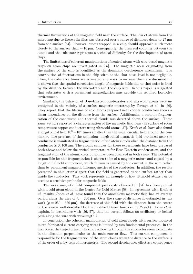
Type (1) Type (2) Type (3)
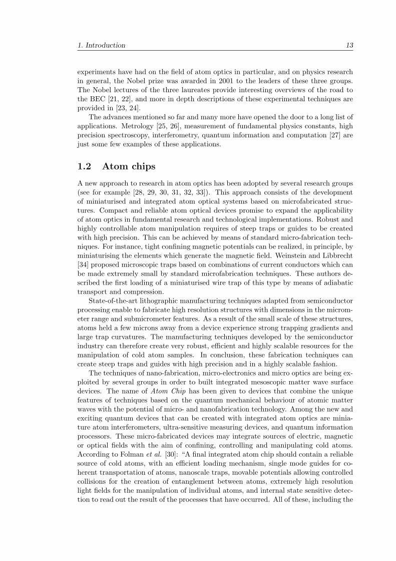
Figure 1.1: Examples of the three ray types generated in a 70.5! pyramid. Inthese images, a top view of a hollow 70.5! pyramid is presented with the pathsthat light incident parallel to the pyramid axis can follow as it is reflectedfrom the hollow surface. Type (1) and type (2) rays are only reflected by twoopposing faces of the pyramid, while type (3) rays su"er reflections on three ofthe four pyramid faces.
As both the loss of atoms and the heating of the cloud are desired to be kept aslow as possible, properly matching the di"erent stages of the loading process turnsout to be a very meticulous, tedious, and time consuming task. As the atom chipfabrication techniques have been refined, it has been possible to attain atom-surfacedistances on the order of a few micrometers. This also means that tighter traps arecreated and consequently, fewer number of atoms are held in these traps. In order todetect, manipulate and controllably modify the internal states of atoms in these tinyclouds it is necessary to make them interact with light. In the experimental sequenceoutlined before, the laser light is delivered to the chip by means of external mirrors andlenses. As the atom-surface distance becomes small and fewer numbers of atoms areconfined in these traps, detection and further manipulation tasks become very di!cult.In response to these complications, the necessity of integrating, not only the sourcesof the trapping potentials, but also optical components into the atom chip has beenpointed out in various publications [35, 36, 59].
Arrays of pyramidal pits have been fabricated in silicon wafers. A gold coating waslaid on these pyramids to create an array of pyramidal hollow mirrors. We believe thatthese pyramids can be the main building block of an e!cient mechanism for loadingcold atom clouds right at the surface of an atom chip. We have studied in detail theoptical properties of the pyramids fabricated in silicon wafers. Firstly, the angle betweenopposite faces in these pyramids is of 70.5!, instead of 90! as in the usual pyramid MOTarrangement [70, 71]. This has consequences on the light force balance produced insidethe micro-fabricated mirrors. To begin with, a ray tracing analysis of this pyramidalgeometry allowed us to identify three di"erent types of pyramid reflections. An exampleof these ray types is given in figure 1.1. Type (1) and type (2) rays, those which arereflected exclusively by opposing faces of the pyramid, create a force balance alongthe pyramid axis and can therefore generate magneto-optical traps. In contrast, thethird reflection type is reflected by three of the four pyramid faces. This type of ray isseverely a"ected both in its propagation direction and in its polarisation state along itspath inside the pyramid. The reflected intensity pattern generated when a laser beamis shone parallel to the pyramid axis shows contributions from the three ray types, asanticipated by the ray tracing analysis.
1. Introduction 21
We have studied both theoretically and experimentally the appropriateness of the70.5! pyramidal geometry for the generation of magneto-optical traps [72]. For this,we fabricated a large scale glass replica of the geometry generated in the silicon micro-mirrors. In addition, for comparison purposes, we also fabricated a pyramid with a 90!
angle between its faces. We have proved that in order to create magneto-optical traps insilicon pyramids, it is necessary to eliminate or reduce the third type of rays. The firstmethod that we proposed for this is to lay a low reflectivity coating on the surface ofthese pyramids. The third ray type is reflected three times by the pyramid faces beforecrossing through the pyramid axis, where the MOT is supposed to be generated. Onthe other hand, the first two ray types cross twice through the trapping region, the firsttime after just one reflection and the second after being reflected twice. Consequently,if a low reflectivity coating is utilised, the intensity of the third ray type, in comparisonwith the other two ray types, is severely reduced before reaching the trapping region.In our large scale replica of the silicon pyramid we tested various reflectivity coatingsand found that an ! 80% reflectivity gives the best results.
The second method that we proposed for taking care of these undesired light com-ponents consists of completely eliminating the areas of the light which give rise to thesereflections. We first demonstrated the e!cacy of this approach by placing a mask onthe trapping beam utilised for creating the MOT in the large pyramid replica. In thisexperiment we found that a high reflectivity gold coating, which does not generate aMOT in the 70.5! when the full beam is shone into it, can be made to work if thetype three ray areas of the beam are masked. We confirmed this result both by placinga mask on the trapping beam and by masking the pyramid surface at the moment oflaying down the metallic coating.
We have also estimated the number of atoms that can be collected in a miniature sil-icon pyramid. We modelled numerically the scattering forces generated in the volume ofthese pyramidal hollow mirrors when circularly polarised light is shone perpendicularlyto the chip surface and a quadrupole magnetic field is generated in the pyramid region.To confirm these estimations, we have mimicked experimentally the tiny pyramids us-ing the large scale pyramid replica. Taking advantage of the pyramidal symmetry, wehave placed the centre of the MOT magnetic quadrupole a few millimetres away fromthe pyramid apex. Then, scaling laws for the number of atoms collected in pyramidsof di"erent sizes have been determined by displacing the quadrupole centre positionsalong the pyramid axis. These experiments have allowed us to establish an empiricalscaling law for the number of atoms that can be collected in a 70.5! pyramidal MOT.In addition, we have studied in detail the capture and loss rates as a function of thepyramid size, for pyramids which side length goes from 16 mm and down to about 3 mm.With this scaling law we anticipate that these traps can in principle collect as many asa few hundred atoms and as few as a single atom.
The first prototype of an atom chip with pyramids integrated on its surface hasbeen designed and fabricated. Together with these micro-fabricated pyramids, thisatom chip integrates also micro-fabricated current carrying wires circling the pyramidsquare openings. We show that the field generated by these wires is equivalent to squareclosed loops running along the edge of the pyramid apertures. Therefore, a bias fieldperpendicular to the chip surface can be utilised together with these wires to generatean spherical quadrupole field inside the pyramid. This configuration creates two pointsof zero magnetic field. Both points are located on the pyramid axis, one inside of thepyramid and the second one outside of the pyramid. This extra feature can in principle
1. Introduction 22
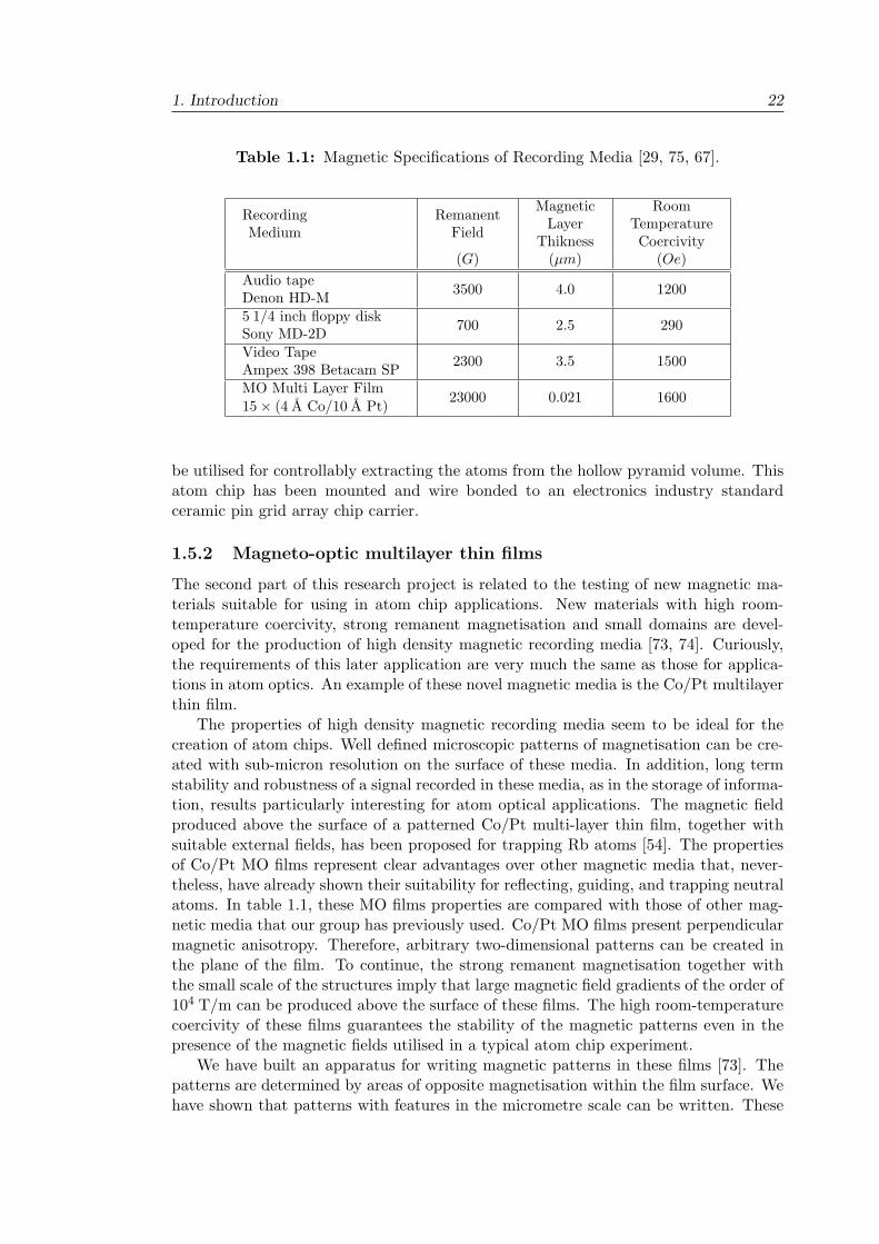
Table 1.1: Magnetic Specifications of Recording Media [29, 75, 67].
RecordingMedium
RemanentField
MagneticLayer
Thikness
RoomTemperatureCoercivity
(G) (µm) (Oe)Audio tapeDenon HD-M 3500 4.0 1200
5 1/4 inch floppy diskSony MD-2D 700 2.5 290
Video TapeAmpex 398 Betacam SP 2300 3.5 1500
MO Multi Layer Film15# (4 A Co/10 A Pt) 23000 0.021 1600
be utilised for controllably extracting the atoms from the hollow pyramid volume. Thisatom chip has been mounted and wire bonded to an electronics industry standardceramic pin grid array chip carrier.
1.5.2 Magneto-optic multilayer thin films
The second part of this research project is related to the testing of new magnetic ma-terials suitable for using in atom chip applications. New materials with high room-temperature coercivity, strong remanent magnetisation and small domains are devel-oped for the production of high density magnetic recording media [73, 74]. Curiously,the requirements of this later application are very much the same as those for applica-tions in atom optics. An example of these novel magnetic media is the Co/Pt multilayerthin film.
The properties of high density magnetic recording media seem to be ideal for thecreation of atom chips. Well defined microscopic patterns of magnetisation can be cre-ated with sub-micron resolution on the surface of these media. In addition, long termstability and robustness of a signal recorded in these media, as in the storage of informa-tion, results particularly interesting for atom optical applications. The magnetic fieldproduced above the surface of a patterned Co/Pt multi-layer thin film, together withsuitable external fields, has been proposed for trapping Rb atoms [54]. The propertiesof Co/Pt MO films represent clear advantages over other magnetic media that, never-theless, have already shown their suitability for reflecting, guiding, and trapping neutralatoms. In table 1.1, these MO films properties are compared with those of other mag-netic media that our group has previously used. Co/Pt MO films present perpendicularmagnetic anisotropy. Therefore, arbitrary two-dimensional patterns can be created inthe plane of the film. To continue, the strong remanent magnetisation together withthe small scale of the structures imply that large magnetic field gradients of the order of104 T/m can be produced above the surface of these films. The high room-temperaturecoercivity of these films guarantees the stability of the magnetic patterns even in thepresence of the magnetic fields utilised in a typical atom chip experiment.
We have built an apparatus for writing magnetic patterns in these films [73]. Thepatterns are determined by areas of opposite magnetisation within the film surface. Wehave shown that patterns with features in the micrometre scale can be written. These
1. Introduction 23
patterns can be scaled up to millimetre dimensions. Two di"erent patterns have beencreated. The first consists of a large array of parallel lines such as the signal recorded inthe video tape atom chip. However, the features recorded in the Co/Pt film are muchsmaller than those present in the video tape and the high remanent magnetisation of theMO film promise higher trap frequencies. The second pattern that we have created is anarray of Z-like patterns, which result in Io"e-Pritchard type traps above the film surface.We have performed numerical estimations of the atom traps that can be generated abovethese magnetic patterns.
We demonstrated that magnetic micro-traps can be generated above the surfaceof magneto-optical Co/Pt thin films [76]. In this thesis, I will describe the apparatusused for writing the magnetisation patterns on the surface to these MO films. Thesepatterns have features of a few microns and numerical calculations of the steep trappingpotentials that can be generated above them has been developed. At a distance of750 nm from the chip surface, these traps can be as deep as 3 mK and have harmonicfrequencies of up to 1.1 MHz. The domain structure of these magnetic films seems to bethe limiting factor of the patterns quality. We show that the borders between regions ofopposite magnetisation present transverse oscillations which dimensions are comparableto the domain structure observed in a demagnetised sample.
1.6 Organization of this thesis
In the following paragraphs I describe the contents of this thesis.To begin with, the theory of laser cooling and trapping of neutral atoms is given in
chapter 2. The scattering force is the starting point for explaining the concept of Dopplercooling. Next, the processes involved in subDoppler cooling are briefly described. Tocontinue, the magneto-optic trap (MOT) operation principles are introduced. Particu-larly, the filling dynamics of the MOT are studied in some detail. Finally, some relevantconcepts regarding magnetic trapping of neutral atoms are studied with the aim ofsetting the basic requirements utilised in the design of atom chips.
Chapter 3 contains a description of the experimental resources that have been builtas part of my research project. This begins with the design and construction of boththe vacuum and the laser systems; next, the procedure for making glass pyramids isdescribed together with the analysis of the resulting hollow mirrors; in the third place,I present the various magnetic field sources utilised in our experiments and how theywere used for achieving the required field configurations; this chapter concludes with adescription of the methodology used for imaging of cold atom clouds.
Chapter 4 reports the experiments performed to determine the suitability of thesilicon hollow pyramidal mirrors for applications in atom optics. In this chapter I firstdemonstrate that cold rubidium clouds can be magneto-optically trapped in a 70.5!
pyramid. Then, I also present the results obtained by coating both the 70.5! andthe 90! pyramids with di"erent metallic coatings. Here, it is also shown under whichcircumstances the MOT works in a 70.5! pyramid covered with a highly reflective goldcoating. Next, the chapter continues with an experimental determination of the scalinglaws for the number of atoms versus the size of the pyramids. Capture and loss ratesmeasurements are then provided and these results are used to estimate the number ofatoms that can be trapped in an atom chip pyramid.
Chapter 5 begins with a brief description of the fabrication of pyramids in siliconwafers. Then, the chapter continuous analysing both the geometrical and optical prop-
1. Introduction 24
erties of the resulting pyramids, as well as these properties implications on the MOTperformance. The first prototype of a pyramid atom chip, which integrates micro-fabricated pyramids and wires, is shown next. This is accompanied with a detail de-scription and characterisation of the resources utilised for incorporating the atom chipinto our vacuum system.
An introduction to the physics of magneto-optic thin films is provided at the begin-ning of chapter 6. After this, the focus of the chapter is narrowed around the charac-teristics of the Co/Pt multilayer films that we have fabricated. The thermo-magneticrecording technique utilised for writing magnetisation patterns in these MO films occu-pies a separate section of the chapter. Then, I present the two di"erent patterns thatwe have created. A detailed analysis of the magnetic trapping potentials that can begenerated above these patterns is provided.
To conclude, chapter 7 summarizes the most important results of this researchproject. Here, I discuss the place that these achievements occupy in atom optics re-search, and particularly in the development of atom chips. In addition, this chapteridentifies the future directions of this research and the challenges that this particularproject faces.
25
Chapter 2
Cooling, trapping andmanipulating atoms
In this chapter, I describe the basic theory involved in atom optics. Firstly, the two-level atom laser cooling model is used for introducing the concepts of Doppler coolingand optical molasses. Then this model is extended to multilevel atoms for explaining thesub-Doppler cooling mechanisms. Next, I explain how a magnetic field can work togetherwith the optical field for trapping atom clouds in a magneto-optical trap (MOT). Then,the MOT filling dynamics are analysed. In addition, I also provide an introduction tothe Physics of magnetostatic trapping neutral atoms. Finally, I conclude this chapterby discussing the miniaturization of MOTs and magnetic traps.
2.1 The scattering force
The scattering force that a laser light field exerts on an atom is the basis of a method forcooling atoms. As Metcalf and Van der Straten explain in [77], when an atom absorbsa photon, it gains a momentum !k in the direction of the laser beam, where k = 2!
" kis the wave vector of light with wavelength %. Over many absorption cycles, the time-averaged force exerted on an atom by a laser beam is equal to the momentum kick !keach photon exerts on the atom times the rate at which the absorption and emissionprocess takes place. This force is then 'F = !k#, where # is the total scattering rate.In sponataneous emission however, the time-average momentum gain experienced bythis atom is zero because photons are emitted symmetrically in all directions. The totalscattering rate # can be expressed in terms of both the laser intensity I and the detuningfrom the atomic transition $ as measured in the atom frame of reference:
#(I,$) =(
2I/Isat
1 + I/Isat + (2$/()2(2.1)
In this equation, ( is the spontaneous emission rate (" = 1/( is the excited statelifetime) and Isat is the saturation intensity of the atomic transition, which is defined
2. Cooling, trapping and manipulating atoms 26
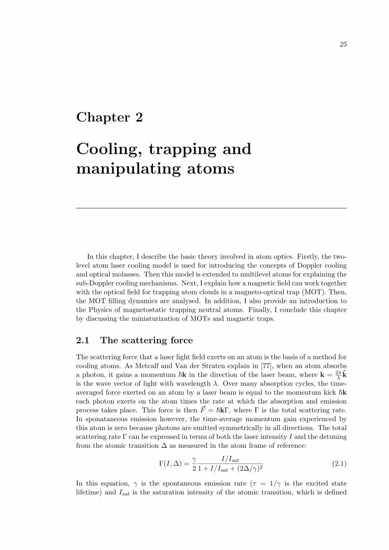
Figure 2.1: The time-averaged force ona two-level atom in a 1D optical molasses.The forces exerted by each light beam in-dividually are shown as blue dotted linesand the solid line corresponds to the totalforce given by equation 2.4. The linear ap-proximation (equation 2.5) is representedas a dashed straight line.
as the laser intensity value which generates an excited state population fraction of 1/4at zero detuning. For a two level atom, Isat is given by
Isat =&hc(
3%3. (2.2)
In conclusion, the scattering force experienced by an atom at rest turns out to be
F =!k(
2s0
1 + s0 + (2$/()2(2.3)
where the on-resonance saturation parameter is s0 = I/Isat.
2.1.1 Doppler cooling and optical molasses
The scattering force depends on the Doppler shift )D of the laser frequency as experi-enced in the reference frame of a moving atom. The wavelength of the light measured inthe reference frame of an atom moving away from the source of the light is longer thanthe actual wavelength measured in a reference frame at rest. Similarly, an atom movingtowards the light source witnesses the opposite shift of the wavelength of the light. Asa result of this shifts, the scattering rate depends on the velocity of the atom and onthe detuning of the laser frequency from the atomic transition. The laser frequency inthe reference frame of the moving atom is Doppler shifted, which results in a detuning$D = ()# " )a) " k ·v with )# as the laser frequency, )a as the atomic transition fre-quency in the absence of a magnetic field, and k ·v as the first order Doppler shift. Forred detuned light ()# < )a) the atom is more likely to absorb photons from the beamwhose propagation direction opposes the motion of the atom. Therefore, a detuning ofthe laser frequency around the atomic transition can be used to selectively reduce thevelocity of those atoms moving against the light. This method for reducing the kineticenergy of a sample of atoms is known as Doppler Cooling [77].
Let * = )#")a be the detuning of the laser frequency from the atomic transitions asmeasured on a reference frame at rest. Then, the one-dimensional time-averaged forceon a two-level atom due to a counter-propagating pair of beams can be written as
Fx =!kx(
2
!
" s0
1 + s0 + 4($"kxvx)2
%2
" s0
1 + s0 + 4($+kxvx)2
%2
#
$ . (2.4)
2. Cooling, trapping and manipulating atoms 27
This force can be expanded as a Taylor series in vx around vx = 0. Retaining only thelinear term of this expansion gives
Fx = "8!*k2x
(
s0%1 + s0 + 4$2
%2
&2 vx = "#vx (2.5)
This shows that the average force tends to damp the motion of atoms in the directionof the laser field, where we have defined # as the damping constant. The total forceexpressed in equation 2.4 is plotted in figure 2.1 as a solid curve, together with thecontributions from each one of the two laser beams that are shown as dotted curves.The dashed straight line is the first order Taylor expansion (equation 2.5) which showsthe restoring nature of this force.
If the laser field consists of three pairs of counter propagating beams, each pairaligned orthogonal to others, the force acts on each of the three spatial degrees offreedom of these atoms. The analysis presented previously can be easily extendedto three dimensions. This creates a region, the intersection of the six laser beams,where the motion of the atoms experiences a viscous damping. This is known as anoptical molasses [5]. A cold atom cloud forms in the optical molasses having a velocitydistribution which is generally Maxwellian. A temperature T can be assigned to thevelocity distribution, which for an n-dimensional trap is
n
2kBT =
n'
i=1
m
2v2i (2.6)
Here, the thermal energy per degree of freedom is 12kBT and vi is the r.m.s. velocity in
the ith direction.The minimum temperature achievable with Doppler cooling is reached when the rate
of removal of kinetic energy by the damping force is balanced by the heating rate dueto the random nature of the absorption and emission of photons. Due to the discretenature of atom-photon interaction, the cycles of absorption and emission of photons areseen by the atom as two steps of a random walk in momentum space [77]. The sizeof these steps is given by the momentum kick !k induced in the atoms. After N suchkicks, the atom r.m.s. momentum grows as
%N!k. Therefore, the condition of balance
between the damping force and the heating rate leads to the Doppler Temperature [77]
TD =!(
4kB
1 + I/ISat + (2*/()2
2|*|/((2.7)
In the low intensity limit and for * = "(/2, the Doppler temperature is minimal andis reduced to TD = !(/2kB. For example, the 5P3/2 state of 85Rb and 87Rb are char-acterised by spontaneous decay rates equal to ( = 5.98 MHz and ( = 6.07 MHz respec-tively. Correspondingly, the minimal Doppler temperature associated to the D2 line ofthese two rubidium isotopes is TD = 143 µK and TD = 145 µK respectively.
2.2 Sub-Doppler cooling
The variety of processes taking place in optical molasses is much richer than this two levelatom model. In a real atom, energy shifts in the hyperfine sublevels can be induced byperturbing fields, such as light or an external magnetic field. The multilevel atom pictureis then more adequate for distinguishing the more subtle details of these experiments.
2. Cooling, trapping and manipulating atoms 28
2.2.1 Polarization gradient cooling
When considering the multilevel atom, temperatures below TD can be achieved throughthe interaction between the atom hyperfine structure and the spatial variation of thelight polarisation in optical molasses. This mechanism, called Polarization GradientCooling, operates in low magnetic fields (| B |< 100 mG) and with an optimum detuninggreater than that for Doppler cooling. Polarisation gradient cooling can lower theminimum temperature by a large factor compared to that predicted by Doppler coolingtheory [7, 77].
The variation of the light intensity in optical molasses induces AC Stark shifts in theatomic energy sublevels. Due to these shifts, atoms experience an exchange of kineticfor internal potential energy as they move through the light field. As the atoms moveacross the polarisation gradients of the light field, the shift tunes the atomic energylevels to the frequency of the light and, at the point of maximum potential energy,these atoms are optically pumped into a state of lower energy. The energy stored in theinternal structure of the atom has now been liberated and its initial kinetic energy islost. As the atom moves trough the changing polarisation of the light field, it continueslosing energy in successive cycles of shifts and optically pumped transitions. A detaileddescription of this cooling mechanism is given in [7]. The recoil of one photon thencorresponds to the lowest theoretically achievable temperature by sub-Doppler cooling:
Trecoil =!2k2
kBm(2.8)
For 87Rb Trecoil = 361 nK and for 85Rb Trecoil = 370 nK. Note that this new limit isfour hundred times lower than the one given by the Doppler temperature.
2.3 The magneto-optic trap (MOT)
In a magneto-optic trap (MOT), the exchange of momentum is produced in a wide rangeof distances and velocities. The change in the Doppler shift of the decelerated atoms iscompensated by introducing a Zeeman shift [77]. A spherical quadrupole magnetic fieldis in general utilised for generating this compensation. This field consists of a point ofzero magnetic field located in the centre of the quadrupole, with the field increasinglinearly with position as one moves radially from the centre. Consequently, the Zeemanshift is induced by the movement of the atoms in the inhomogeneous magnetic field.The Zeeman interaction energy is given by "µ ·B, where B is the spatially varyingmagnetic field and µ is the atomic magnetic dipole moment. Therefore, the e"ectivedetuning between the atomic cooling transition and the laser field in this situation isgiven by
$Z = * " k ·v " µ ·B (2.9)
Substituting this detuning in equation 2.3 results in a force that depends on both thevelocity and the position of the atoms.
Provided that the magnetic field magnitude B is ! 300 Gauss, the interaction of amoving atom with the magnetic field can be approximated by the first-order Zeemanshift. The splitting between a pair of magnetic sublevels can be written as )Z = "µ#B/!,where µ# & (mege "mggg)µB is the e"ective magnetic moment of the transition. Here,mg,e and gg,e are the magnetic quantum numbers and the Lande factors of the groundg and the excited e states respectively.
2. Cooling, trapping and manipulating atoms 29
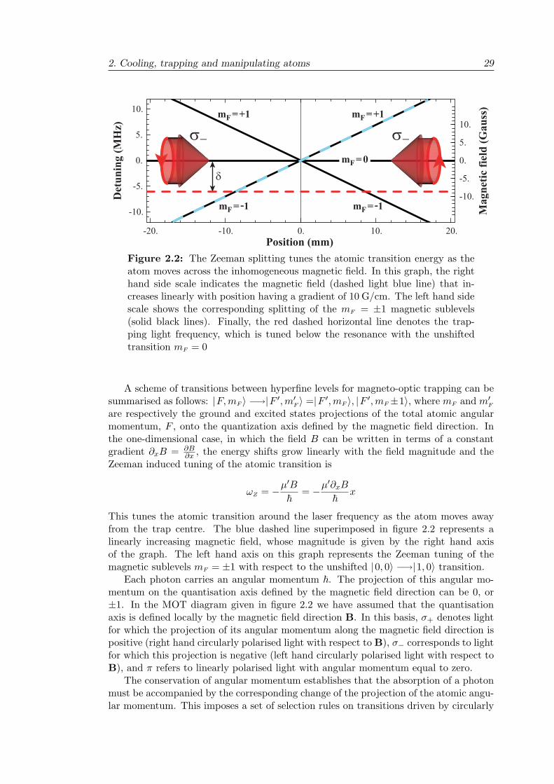
-20. -10. 0. 10. 20.Position (mm)
-10.
-5.
0.
5.
10.D
etu
nin
g (
MH
z)
-10.
-5.
0.
5.
10.
Magn
etic
fie
ld (
Gau
ss)
mF
= +1
mF
= -1
mF
= 0
mF
= -1
mF
= +1
Figure 2.2: The Zeeman splitting tunes the atomic transition energy as theatom moves across the inhomogeneous magnetic field. In this graph, the righthand side scale indicates the magnetic field (dashed light blue line) that in-creases linearly with position having a gradient of 10 G/cm. The left hand sidescale shows the corresponding splitting of the mF = ±1 magnetic sublevels(solid black lines). Finally, the red dashed horizontal line denotes the trap-ping light frequency, which is tuned below the resonance with the unshiftedtransition mF = 0
A scheme of transitions between hyperfine levels for magneto-optic trapping can besummarised as follows: |F,mF ' "(|F #, m#
F ' =|F #, mF ', |F #, mF ±1', where mF and m#F
are respectively the ground and excited states projections of the total atomic angularmomentum, F , onto the quantization axis defined by the magnetic field direction. Inthe one-dimensional case, in which the field B can be written in terms of a constantgradient +xB = &B
&x , the energy shifts grow linearly with the field magnitude and theZeeman induced tuning of the atomic transition is
)Z = "µ#B
! = "µ#+xB
! x
This tunes the atomic transition around the laser frequency as the atom moves awayfrom the trap centre. The blue dashed line superimposed in figure 2.2 represents alinearly increasing magnetic field, whose magnitude is given by the right hand axisof the graph. The left hand axis on this graph represents the Zeeman tuning of themagnetic sublevels mF = ±1 with respect to the unshifted |0, 0' "(|1, 0' transition.
Each photon carries an angular momentum !. The projection of this angular mo-mentum on the quantisation axis defined by the magnetic field direction can be 0, or±1. In the MOT diagram given in figure 2.2 we have assumed that the quantisationaxis is defined locally by the magnetic field direction B. In this basis, ,+ denotes lightfor which the projection of its angular momentum along the magnetic field direction ispositive (right hand circularly polarised light with respect to B), ," corresponds to lightfor which this projection is negative (left hand circularly polarised light with respect toB), and & refers to linearly polarised light with angular momentum equal to zero.
The conservation of angular momentum establishes that the absorption of a photonmust be accompanied by the corresponding change of the projection of the atomic angu-lar momentum. This imposes a set of selection rules on transitions driven by circularly
2. Cooling, trapping and manipulating atoms 30
and linearly polarised light. Firstly, ,+ light drives $mF = +1 transitions; next, ,"light drives $mF = "1 transitions; and finally, for & light $mF = 0. The dashedhorizontal line included in figure 2.2 represents light that is red detuned (detuning *)from the |0, 0' "(|1, 0' transition. Then, if an atom moves away from the trap centrein the positive direction it preferentially absorbs ," photons from the beam travellingtowards the left. Likewise, if the atom moves away from the trap centre along thenegative direction it will preferentially absorb ," photons from the beam that travelstowards the right.
2.3.1 The one-dimensional analysis of the MOT
The one-dimensional treatment of the optical molasses introduced in section 2.1.1 canbe extended to take into account the Zeeman shift generated in the presence of aninhomogeneous magnetic field. The linearly increasing field strength creates a spatialdependence in the detuning term of the scattering rate given in equation 2.1. Thisproduces a confining force that points towards the centre of the trap and makes itpossible to cool and trap atoms simultaneously. Including the first-order Zeeman shift,the detuning term becomes
$± = * ) kv ± µ#B/!
where the + and " subindexes refer to the right going and the left going beams respec-tively. Equation 2.3 can be used to write down the force exerted by each beam on theatoms
F± = ±!k(
2s0
1 + s0 + (2$±/()2, (2.10)
and the total force would beF = F+ + F"
A first order series expansion in v around v = 0 of this force results in a velocityindependent term that can be identified with a restoring force characterised by a springconstant
! = µ#+xB8ks0*
(%1 + s0 + 4$2
%2
&2 , (2.11)
Similarly, as found in the analysis of the optical molasses (see equation 2.5), the velocitydependent term is identified with a damping coe!cient
# =8k2s0*!
(%1 + s0 + 4$2
%2
&2 (2.12)
The force around the MOT centre is therefore approximated by
F * "#v " !x, (2.13)
which leads to damped harmonic motion of the atoms. For 85Rb atoms with s0 = 1,a detuning * = (/2 and a field gradient +xB = 10 G/cm, the damping rate of thismotion (#MOT = #/M) is 21 kHz and the oscillation frequency ()MOT =
(!/M) is less
than 5 kHz. This corresponds to overdamped motion with a restoring time to the trapcentre 2k/µ#+xB = 1.8 ms. In addition, under this simplified model of the MOT we canconclude that a trap of radius R has a depth U0 = 1
2!R2 and a capture velocity vc = 'RM .
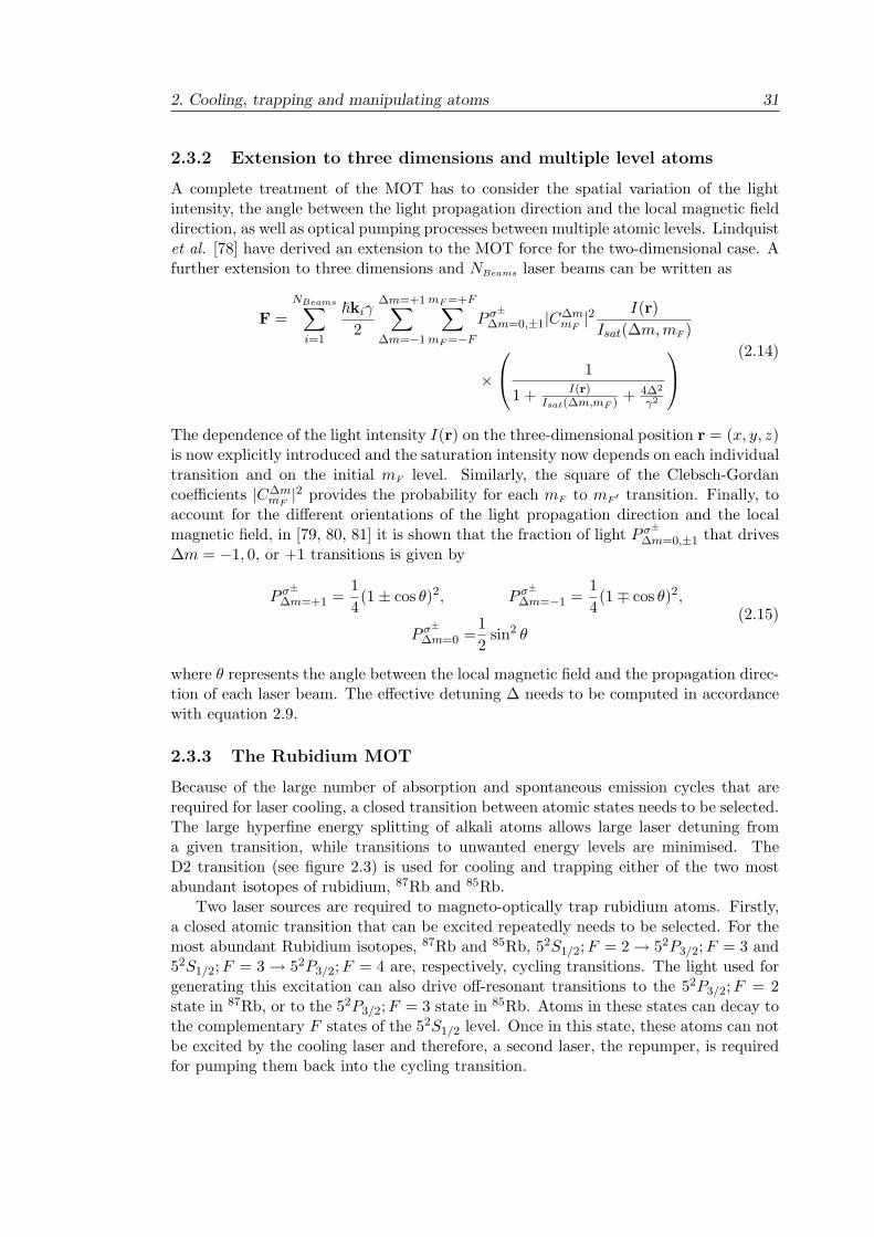
2. Cooling, trapping and manipulating atoms 31
2.3.2 Extension to three dimensions and multiple level atoms
A complete treatment of the MOT has to consider the spatial variation of the lightintensity, the angle between the light propagation direction and the local magnetic fielddirection, as well as optical pumping processes between multiple atomic levels. Lindquistet al. [78] have derived an extension to the MOT force for the two-dimensional case. Afurther extension to three dimensions and NBeams laser beams can be written as
F =NBeams'
i=1
!ki(
2
!m=+1'
!m="1
mF =+F'
mF ="F
P (±!m=0,±1|C!m
mF|2 I(r)
Isat($m, mF )
#
!
" 1
1 + I(r)Isat(!m,mF ) + 4!2
%2
#
$(2.14)
The dependence of the light intensity I(r) on the three-dimensional position r = (x, y, z)is now explicitly introduced and the saturation intensity now depends on each individualtransition and on the initial mF level. Similarly, the square of the Clebsch-Gordancoe!cients |C!m
mF|2 provides the probability for each mF to mF ! transition. Finally, to
account for the di"erent orientations of the light propagation direction and the localmagnetic field, in [79, 80, 81] it is shown that the fraction of light P (±
!m=0,±1 that drives$m = "1, 0, or +1 transitions is given by
P (±!m=+1 =
14(1 ± cos -)2, P (±
!m="1 =14(1) cos -)2,
P (±!m=0 =
12
sin2 -(2.15)
where - represents the angle between the local magnetic field and the propagation direc-tion of each laser beam. The e"ective detuning $ needs to be computed in accordancewith equation 2.9.
2.3.3 The Rubidium MOT
Because of the large number of absorption and spontaneous emission cycles that arerequired for laser cooling, a closed transition between atomic states needs to be selected.The large hyperfine energy splitting of alkali atoms allows large laser detuning froma given transition, while transitions to unwanted energy levels are minimised. TheD2 transition (see figure 2.3) is used for cooling and trapping either of the two mostabundant isotopes of rubidium, 87Rb and 85Rb.
Two laser sources are required to magneto-optically trap rubidium atoms. Firstly,a closed atomic transition that can be excited repeatedly needs to be selected. For themost abundant Rubidium isotopes, 87Rb and 85Rb, 52S1/2;F = 2( 52P3/2;F = 3 and52S1/2;F = 3 ( 52P3/2;F = 4 are, respectively, cycling transitions. The light used forgenerating this excitation can also drive o"-resonant transitions to the 52P3/2;F = 2state in 87Rb, or to the 52P3/2;F = 3 state in 85Rb. Atoms in these states can decay tothe complementary F states of the 52S1/2 level. Once in this state, these atoms can notbe excited by the cooling laser and therefore, a second laser, the repumper, is requiredfor pumping them back into the cycling transition.
2. Cooling, trapping and manipulating atoms 32
2
3151 Mhz
362 Mhz
12
3
4
100 Mhz
29 Mhz
63 Mhz
121 Mhz
2
31265 Mhz
3036 Mhz
01
2
3194 Mhz
72 Mhz
157 Mhz
267 Mhz
1
22563 Mhz
6835 Mhz
1
2305 Mhz
813 Mhz
85Rb (72%) 87Rb (28%)
5 2S1/2 5 2S1/2
5 2P1/2 5 2P1/2
5 2P3/25 2P3/2
F F
Cyclingtransition
Repumptransition
Repumptransition
Cyclingtransition
D1
D2D2
D1
D1 line: 794.98 nm D2 line: 780.025 nm
Figure 2.3: The rubidium energy levels [82].
2.4 The MOT filling rate equation
The change in the number of atoms N collected in a MOT is equal to the di"erencebetween the rate at which atoms are captured and the rate at which atoms are lost.The MOT filling rate equation can be expressed [79, 83] as
dN
dt= R" N
"" .
N2
V(2.16)
The capture rate and the trap lifetime are represented as R and " respectively. The thirdterm in eq. 2.16 corresponds to the losses resulting from two-body collisions betweenatoms in the trap, where V is the volume occupied by the atom cloud. Steane etal. [79] explain that this term is significant at high densities of trapped atoms. Incontrast, when . N2
V is insignificant compared with the first two terms in eq. 2.16, theloss rate is independent of the number of atoms contained in the trap. Under thesecircumstances, the capture rate R and the trap life time " determine the MOT fillingdynamics. Neglecting the third term in the rate equation, the solution to eq. 2.16 is
N(t) = Ns(1" e"t/) ) (2.17)
where Ns = R" is the steady state number of atoms in the MOT.
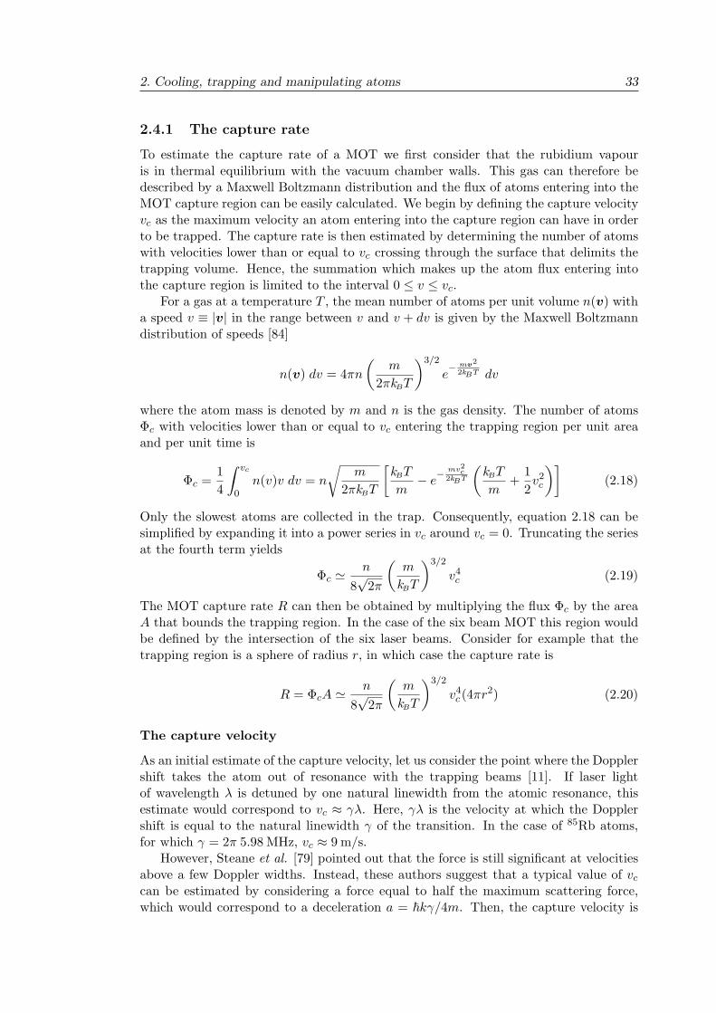
2. Cooling, trapping and manipulating atoms 33
2.4.1 The capture rate
To estimate the capture rate of a MOT we first consider that the rubidium vapouris in thermal equilibrium with the vacuum chamber walls. This gas can therefore bedescribed by a Maxwell Boltzmann distribution and the flux of atoms entering into theMOT capture region can be easily calculated. We begin by defining the capture velocityvc as the maximum velocity an atom entering into the capture region can have in orderto be trapped. The capture rate is then estimated by determining the number of atomswith velocities lower than or equal to vc crossing through the surface that delimits thetrapping volume. Hence, the summation which makes up the atom flux entering intothe capture region is limited to the interval 0 $ v $ vc.
For a gas at a temperature T , the mean number of atoms per unit volume n(v) witha speed v & |v| in the range between v and v + dv is given by the Maxwell Boltzmanndistribution of speeds [84]
n(v) dv = 4&n
)m
2&kBT
*3/2
e" mv2
2kBT dv
where the atom mass is denoted by m and n is the gas density. The number of atoms%c with velocities lower than or equal to vc entering the trapping region per unit areaand per unit time is
%c =14
+ vc
0n(v)v dv = n
,m
2&kBT
-kBT
m" e
" mv2c
2kBT
)kBT
m+
12v2c
*.(2.18)
Only the slowest atoms are collected in the trap. Consequently, equation 2.18 can besimplified by expanding it into a power series in vc around vc = 0. Truncating the seriesat the fourth term yields
%c +n
8%
2&
)m
kBT
*3/2
v4c (2.19)
The MOT capture rate R can then be obtained by multiplying the flux %c by the areaA that bounds the trapping region. In the case of the six beam MOT this region wouldbe defined by the intersection of the six laser beams. Consider for example that thetrapping region is a sphere of radius r, in which case the capture rate is
R = %cA +n
8%
2&
)m
kBT
*3/2
v4c (4&r2) (2.20)
The capture velocity
As an initial estimate of the capture velocity, let us consider the point where the Dopplershift takes the atom out of resonance with the trapping beams [11]. If laser lightof wavelength % is detuned by one natural linewidth from the atomic resonance, thisestimate would correspond to vc * (%. Here, (% is the velocity at which the Dopplershift is equal to the natural linewidth ( of the transition. In the case of 85Rb atoms,for which ( = 2& 5.98 MHz, vc * 9 m/s.
However, Steane et al. [79] pointed out that the force is still significant at velocitiesabove a few Doppler widths. Instead, these authors suggest that a typical value of vc
can be estimated by considering a force equal to half the maximum scattering force,which would correspond to a deceleration a = !k(/4m. Then, the capture velocity is
2. Cooling, trapping and manipulating atoms 34
identified with the velocity of an atom that is stopped in a distance equal to the radiusr of the trap, vc = (2ar)1/2. For a 85Rb atom and considering a trap radius of 4 mm,this estimation results in vc = 21 m/s.
We can take now this estimate of vc to express the capture rate derived before(equation 4.2) in terms of the spherical trapping region radius
R =%
2&
)m
kBT
*3/2 )!k(
4m
*2
n r4 (2.21)
If we consider again a 4 mm in radius spherical trapping region for 85Rb atoms, a capturerate of 4# 107 s"1 for a rubidium partial pressure of 4# 10"9 mbar (n ! 1014 m"3) isobtained by this relation.
2.4.2 The loss rate
The loss mechanisms that normally determine the value of " are due to collisions withRb and non-Rb background atoms. Equation 2.16 with no loading term and neglectingthe two body loss term reduces to
dN
dt= "N
"(2.22)
This indicates that the number of atoms in the trap decays exponentially with timeafter the loading is switched o"
N(t) = N0e"t/)
where N0 is the initial number of atoms in the trap.Losses from a trapped atom cloud occur due to collisions with room-temperature
background atoms. The losses caused by collisions with background Rb atoms can beexpressed in terms of the rubidium atom density,
1"Rb
= nRb ,Rb vth = nRb ,Rb
)3 kB T
mRb
*1/2
(2.23)
where ,Rb is the cross section for collisions between a cold trapped atom and a fast back-ground rubidium atom. In addition, this equation makes use of the definition of themean velocity of thermal atoms vth =
(3 kB T/mRb. Similarly, other species contribut-
ing to the background pressure can eject atoms out of the MOT. The characteristic timeof these processes is such that
1"b
= nb ,b
)3 kB T
mb
*1/2
. (2.24)
Consequently, the total amount of losses caused by collisions with all varieties of hotbackground atoms is characterised by the 1/e time in which atoms are ejected from theMOT:
1"
=1
"Rb+
1"b
(2.25)
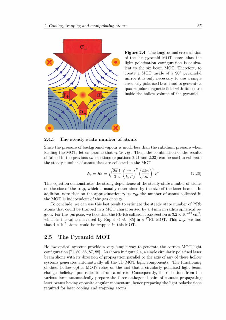
2. Cooling, trapping and manipulating atoms 35
-
++
-Figure 2.4: The longitudinal cross sectionof the 90! pyramid MOT shows that thelight polarisation configuration is equiva-lent to the six beam MOT. Therefore, tocreate a MOT inside of a 90! pyramidalmirror it is only necessary to use a singlecircularly polarised beam and to generate aquadrupolar magnetic field with its centreinside the hollow volume of the pyramid.
2.4.3 The steady state number of atoms
Since the pressure of background vapour is much less than the rubidium pressure whenloading the MOT, let us assume that "b , "Rb. Then, the combination of the resultsobtained in the previous two sections (equations 2.21 and 2.23) can be used to estimatethe steady number of atoms that are collected in the MOT
Ns = R" =,
2&
31,
)m
kBT
*2 )!k(
4m
*2
r4 (2.26)
This equation demonstrates the strong dependence of the steady state number of atomson the size of the trap, which is usually determined by the size of the laser beams. Inaddition, note that on the approximation "b , "Rb the number of atoms collected inthe MOT is independent of the gas density.
To conclude, we can use this last result to estimate the steady state number of 85Rbatoms that could be trapped in a MOT characterised by a 4 mm in radius spherical re-gion. For this purpose, we take that the Rb-Rb collision cross section is 3.2# 10"13 cm2,which is the value measured by Rapol et al. [85] in a 87Rb MOT. This way, we findthat 4# 107 atoms could be trapped in this MOT.
2.5 The Pyramid MOT
Hollow optical systems provide a very simple way to generate the correct MOT lightconfiguration [71, 80, 86, 87, 88]. As shown in figure 2.4, a single circularly polarised laserbeam shone with its direction of propagation parallel to the axis of any of these hollowsystems generates automatically all the 3D MOT light components. The functioningof these hollow optics MOTs relies on the fact that a circularly polarised light beamchanges helicity upon reflection from a mirror. Consequently, the reflections from thevarious faces automatically prepare the three orthogonal pairs of counter propagatinglaser beams having opposite angular momentum, hence preparing the light polarisationsrequired for laser cooling and trapping atoms.
2. Cooling, trapping and manipulating atoms 36
Figure 2.4 also shows the field lines of the quadrupolar magnetic potential generatedby two circular coils running current in opposite directions. The coils are coaxial withthe pyramid axis and are located at opposite sides of the hollow pyramid. This createsa point of zero magnetic field inside the hollow pyramid and the magnetic field strengthgrows linearly with position as one moves away from that point. In order to create aMOT, it is only necessary to ensure that the direction in which these coils current runs,as shown in the scheme, opposes the helicity of the light component that travels towardsthe point of zero magnetic field.
This arrangement represents a great simplification of the MOT system. While in theusual six beam configuration it is necessary not only to align the six light componentsbut also to prepare properly the polarisation of each one of the six beams, in thepyramid MOT it is su!cient with aligning and preparing the circular polarisation ofa single beam. As a result of the inherent simplicity and robustness of these MOTs,90! pyramidal hollow mirrors are used in several atom optics research groups as highlyreliable and extremely robust sources of cold atoms [89], and even in laser cooling andtrapping apparatus for undergraduate laboratories as valuable teaching resources [90].
2.6 Magnetic trapping
Magnetic trapping of neutral atoms depends on the interaction between an inhomoge-neous magnetic field and the atomic magnetic dipole moment. The potential associatedwith this interaction is given by the projection of the atomic magnetic dipole momentµ along the direction of the field B:
U = "µ ·B (2.27)
There are two important consequences of magnetically trapping neutral atoms: first,the atomic energy levels will necessarily shift as the atoms move on the trap; second,practical traps for ground-state neutral atoms are necessarily very shallow comparedwith thermal energy because energy levels shifts are considerable smaller than !BT forT = 1 K [77]. Therefore, atoms must have been collected in a MOT and prepared inthe required state.
The Hamiltonian of the interaction between an atom and a magnetic field consistsof two terms. The first term corresponds to the interaction of the nuclear magneticmoment with the magnetic field generated by the electrons, or hyperfine interaction.The second term describes the interaction between the magnetic field B and the atomicmagnetic moment µ, the Zeeman interaction. In the basis of the total electronic an-gular momentum J and the nuclear angular momentum I states |J, mJ ; I, mI', thisHamiltonian is
H =A
I + 12
I ·J" µ ·B (2.28)
The hyperfine splitting A/h between the F = 1 and F = 2 levels of the 5S1/2 state of87Rb and 85Rb atoms is 6385 MHz and 3036 MHz respectively. The Zeeman interactioncontains electronic and nuclear contributions
µ = "gJµBJ" gIµNI= "gJµBJ + g#IµBI,
(2.29)
where µB = e!/2me is the Bohr magneton; µN = e!/2mp is the nuclear magneton;gJ is the Lande g-factor, which represents the total electronic angular momentum; and
2. Cooling, trapping and manipulating atoms 37
gI is the nuclear angular momentum g-factor. For 87Rb, I = 3/2, gI = 2.751 andg#I = 0.995# 10"3; while for 85Rb, I = 5/2, gI = 1.353 and g#I = 0.293# 10"3 [82, 91].
Taking gs + 2, the Lande g-factor is
gJ = 1 +J(J + 1)" L(L + 1) + S(S + 1)
2J(J + 1)(2.30)
For the 5S1/2 ground state this results in gJ = 2 and for the 5P3/2 state in gJ = 4/3. ForJ = 1
2 , the interaction Hamiltonian can be analytically diagonalised and the energies ofthe magnetic sublevels are given by the Breit-Rabi formula [92]:
E|J=1/2,mJ ;I,mI$ = " hA
2(2I + 1)" g#IµBBmF + ("1)F hA
2
/1 +
2mF
I + 12
x + x2 (2.31)
where x = (gI+gs)µBBhA .
In the limit of low magnetic field (B < 300 G), the Zeeman interaction lifts thedegeneracy in mF and the resulting energy shift can be approximated to first order toobtain
$E(J I) F mF= µBgF mF B (2.32)
where
gF =gJ(F (F + 1) + J(J + 1)" I(I + 1)) + µN
µB(F (F + 1)" J(J + 1) + I(I + 1))
2F (F + 1)(2.33)
Since the ratio µN/µB ! 5# 10"4, the second term in this last expression is negligiblecompared with the first term and this formula can be rewritten as
gF +gJ(F (F + 1) + J(J + 1)" I(I + 1))
2F (F + 1)(2.34)
An atom polarized in a particular Zeeman sublevel is driven by the Stern-Gerlachforce,
F = "-E = "gF mF µF-B (2.35)
Then, atoms for which gF mF > 0 are attracted to regions of low magnetic field. Theseatoms are therefore low field seekers and can be trapped in a minimum of the magneticfield. In addition, the highest mF states are trapped most strongly. For example, 87Rbatoms prepared in the |F,mF ' = |2, 2' state by optical pumping are trapped morestrongly in a magnetic field minimum than in any other state. On the other hand,atoms in a state such that gF mF < 0 are high field seekers.
The adiabatic condition
The confining force an atom experiences in a magnetic trap originates from the in-teraction between the atomic magnetic moment and the nonuniform static field. Theconfinement depends on the maintenance of a given orientation of the atomic momentwith the local field. The energy shift as stated in equation (2.32) is only valid if the pro-jection of the atomic magnetic moment, mF , on the direction of the field is a constant ofthe motion. This implies that to keep an atom trapped, it has to remain adiabaticallyin a given Zeeman sublevel.
2. Cooling, trapping and manipulating atoms 38
When the precession frequency is not large compared with the frequency of orbitalmotion, the desired orientation is lost. This means that spin-flipping transitions betweenmagnetic sublevels do not occur. These transitions are often called Majorana spin flipsand they cause the particle to escape from the trap [16]. Therefore, the atom shouldmove slowly enough to follow the field adiabatically [93].
Let v = (vx, vy, vz) be the velocity of the atom. Then, the variation of the magneticfield in the reference frame of the moving atom is given by
dBdt
=+B+x
vx ++B+y
vy ++B+z
vz (2.36)
This can be expressed in two components, one parallel and one orthogonal to B:
dBdt
= )1B + ! #B, (2.37)
where)1 =
BB2
· dBdt
(2.38a)
and! =
BB2
# dBdt
. (2.38b)
The atomic magnetic moment, µ, precesses about B with the instantaneous Larmorfrequency )0 = |gF mF µB/!|. To avoid any transition between spin states, the fielddirection has to change slowly enough for the magnetic moment of the atom to be ableto follow it adiabatically. The adiabatic condition is then
|!|. )0
This is, 0000BB2
# dBdt
0000 . )0 (2.39)
A general interpretation of )0 is that it is the minimum value of the angular fre-quency of the di"erent allowed transitions between the levels of the quantum systems.The adiabatic condition is generally fulfilled for cold atoms in magnetic traps since therate of change of the magnetic field that any atom experiences is limited by its lowvelocity.
2.7 Magnetic traps in atom chips
There are two main methods for creating magnetic trapping potentials in atom chips:current carrying wires and permanently magnetized surfaces.
2.7.1 Microfabricated current carrying wires
The most elementary tool that can be included in an atom chip is a single straightcurrent carrying wire. Provided that the distance r from the centre of the wire is smallcompared with the wire length, the magnitude of the magnetic field produced by thisstraight flowing current I is simply µ0I/2&r. The direction of the magnetic field vectoris determined by the right hand rule. Therefore, a homogeneous bias field pointing ina direction orthogonal to the wire can be used to create a 2D quadrupole field with a
2. Cooling, trapping and manipulating atoms 39
line of zero magnetic field running next to the wire [59]. The bias field, here denotedby Bbias, determines the distance of the zero magnetic field line as measured from thecentre of the wire
r0 =%µ0
2&
& I
Bbias(2.40)
Similarly, the gradient of the magnetic field around this line is
dB
dr
0000r0
=)
2&
µ0
*B2
bias
I=
Bbias
r0(2.41)
The 2D field minimum generated by the wire can be used to guide neutral atoms ina low field seeking state. To avoid Majorana spin flips at the centre of this guide, wherethe field magnitude is equal to zero, an additional field needs to be included alongthe wire direction. The new field, which we will denote as B0, curves the magneticpotential minimum and creates a Io"e-Pritchard trap. At the field minimum position,the curvature of the field in the direction perpendicular to the wire is given by
d2B
dr2
0000r0
=)
2&
µ0
*2 B4bias
B0I2=
B2bias
r20B0
(2.42)
For an atom of mass M in a low field seeking |F,mF ' state, the harmonic oscillationfrequency at the centre of this guide is
fr =)r
2&=
12&
/µBgF mF
M
)d2B
dr2
*=
12&
/µBgF mF
M
)B2
bias
r20B0
*(2.43)
In consequence, high trap frequencies are achieved when Bbias places the guide close tothe wire. Additionally, the magnitude of B0 must be kept as low as possible in orderto obtain the highest possible frequencies. The depth of this trap is proportional to thedi"erence in magnitude between the field at the centre of the trap, B0, and the field farfrom the wire, Bbias. Consequently, the depth of the trap that a low field seeking atomexperiences is
U0 = µBgF mF (Bbias "B0) (2.44)
The guiding potential can then be transversally closed with the field of two parallelwires running perpendicularly to the direction of the guide. In this way, a new degreeof confinement is imposed on the atomic motion. The axial harmonic frequency of thetrapping potential is given by
fz =)z
2&=
12&
/µBgF mF
M
)d2B
dz2
*(2.45)
The magnetic field generated by a current carrying wire bent in a Z-like shape issimilar to the previous example. In this occasion, a Io"e-Pritchard type trap is formedon top of the wire when a bias field is added in the direction perpendicular to the centralsegment. This configuration has the advantage that it is not necessary to apply anyfurther bias fields. The contributions from both extremes of the Z wire provide an axialbias which is high enough for maintaining the atoms in a strongly trapped state.
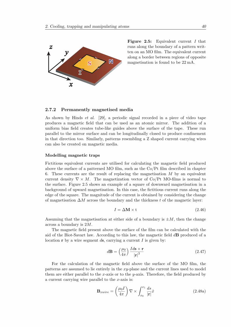
2. Cooling, trapping and manipulating atoms 40
NS
I
x
yz
Figure 2.5: Equivalent current I thatruns along the boundary of a pattern writ-ten on an MO film. The equivalent currentalong a border between regions of oppositemagnetisation is found to be 22 mA.
2.7.2 Permanently magnetised media
As shown by Hinds et al. [29], a periodic signal recorded in a piece of video tapeproduces a magnetic field that can be used as an atomic mirror. The addition of auniform bias field creates tube-like guides above the surface of the tape. These runparallel to the mirror surface and can be longitudinally closed to produce confinementin that direction too. Similarly, patterns resembling a Z shaped current carrying wirescan also be created on magnetic media.
Modelling magnetic traps
Fictitious equivalent currents are utilised for calculating the magnetic field producedabove the surface of a patterned MO film, such as the Co/Pt film described in chapter6. These currents are the result of replacing the magnetisation M by an equivalentcurrent density - # M . The magnetization vector of Co/Pt MO-films is normal tothe surface. Figure 2.5 shows an example of a square of downward magnetisation in abackground of upward magnetisation. In this case, the fictitious current runs along theedge of the square. The magnitude of the current is obtained by considering the changeof magnetisation $M across the boundary and the thickness t of the magnetic layer:
I = $M# t (2.46)
Assuming that the magnetisation at either side of a boundary is ±M , then the changeacross a boundary is 2M .
The magnetic field present above the surface of the film can be calculated with theaid of the Biot-Savart law. According to this law, the magnetic field dB produced of alocation r by a wire segment ds, carrying a current I is given by:
dB =%µ0
4&
& Ids# r|r|3
(2.47)
For the calculation of the magnetic field above the surface of the MO film, thepatterns are assumed to lie entirely in the xy-plane and the current lines used to modelthem are either parallel to the x-axis or to the y-axis. Therefore, the field produced bya current carrying wire parallel to the x-axis is:
Bxwire =)
µ0I
4&
*-#
+ x1
x0
ds
|r| x (2.48a)

2. Cooling, trapping and manipulating atoms 41
Similarly, the field produced by a wire parallel to the y-axis is:
Bywire =)
µ0I
4&
*-#
+ y1
y0
ds
|r| y (2.48b)
In equations (2.48), (x0, x1) and (y0, y1) represent the extension of segments of wirealong the x-axis or along the y-axis respectively.
42
Chapter 3
Experimental apparatus
This chapter contains a description of the apparatus that was developed throughoutthis project. I provide a description of an entirely new vacuum system that was buildexplicitly for testing atom chips. I also describe the dichroic atomic vapour laser locks aswell as polarization and saturation spectroscopy systems that were built for stabilizingthe frequencies of the radiation emitted by three extended cavity diode lasers. Magneticfield sources and electronics for controlling and stabilizing the currents supplied to themare also described in this chapter. Additionally, I describe the imaging system that isessential for the operation of our experiments.
3.1 Vacuum system
To evaluate the di"erent elements of the new generation of atom chips and ultimatelyfor testing our atom chip, we built a new vacuum system. A vacuum on the order of afew 10"9 mbar had to be easily achieved with the atom chip inside the vacuum chamber.
3.1.1 The vacuum chamber
The main element of the vacuum system (figure 3.1) that has been built is an extendedoctagon, multi-CFTM fitting (Kimball Physics Inc., MCF800-EO200080.16-A) UHVvacuum chamber. This chamber includes two 8”, eight 2 3/4”, and sixteen 1 1/3” CFports. With a large internal volume (7.1” diameter spherical workspace) and wideoptical access, this extended octagon is particularly suitable for our application. Thisvacuum system routinely operates at a base pressure below 10"9 mbar and the pumpingdown procedure followed for achieving this pressure is described in appendix A.
Three aluminium posts support the vacuum chamber, placing its geometrical centreapproximately 35 cm above the optics table surface. The two 8” ports of this chamberare parallel to the table surface and a CF anti-reflection coated viewport is attached tothe bottom port. Similarly, CF anti-reflection coated viewports cover seven of the 2 3/4”chamber ports, and a combination of CF anti-reflection coated viewports and blankflanges close the sixteen 11/3” ports. A four way cross is attached to the remaining 23/4”port and the opposite side of this is connected to a 20 Ls"1 ion pump (VacIon Plus 20
3. Experimental apparatus 43
Figure 3.1: The vacuum system. The oc-tagon vacuum chamber rests on three alu-minium posts and the ion pump (on right)is attached to one of the chamber ports.The viewports that seal most of the vac-uum 2 3/4” ports provide appropriate viewaccess to our experiments.
Figure 3.2: The Rubidium dispenser isheld on a macor mount, which is in turnattached to a long aluminium leg by a sin-gle bolt and screw set. Wires on the backof this holder supply electric current to thedispenser. The dispenser terminals andthe wires are sandwiched between copperwashers to guarantee good electrical con-tact. Finally, a thin and straight copperwire in front of the dispenser screens therubidium e"usion.
StarCell). An all-metal CF angle valve and a CF blank flange seal the remaining two2 3/4” ports of the four way cross. Finally, the top 8” port is used for loading the atomchip assembly into the vacuum chamber. This assembly is described in section 5.3.1.
The laboratory coordinate system
We defined a left hand coordinate system with respect to the vacuum chamber with itsorigin at the centre of the octagon. The z axis is vertically upward; the x and y axesare horizontal oriented and the former points towards to the ion pump.
3.1.2 The Rubidium dispenser
We use current heated rubidium dispensers (SAES Getters Rb\NF\4.5\12\FT 10 + 10).This method is suitable for controlling the rubidium partial pressure because the rateof evaporation is reproducible and can be controlled at will. The evaporation process isactivated by heat, which in turn is generated by running current through the dispenserbody. An insulating macor1 block, shown in figure 3.2, was designed for holding therubidium dispenser in the atom chip testing experimental apparatus. This block holdsthe dispenser and directs the atom e"usion. Current carrying wires attached to theback of this block provide electric current to the dispenser, and a wire located in thefront of the block screens the atomic flux. A detailed description of the dispenser holderwill be given in section 3.1.3.
1Macor is a machineable glass-ceramic with good thermal properties and low outgassing rates(www.corning.com).
3. Experimental apparatus 44
5.0 5.2 5.4 5.6 5.8 6.01.0
10.0
P Rb (1
0-9m
bar)
Dispenser current (A)
Figure 3.3: The Rubidium partial pres-sure versus dispenser current calibrationcurve is shown along with the experimen-tal data used to deduce the dependency.To generate the calibration curve, the datapoints were fitted to a simple exponentialgrowth formula.
The dependence of rubidium pressure on dispenser current was carefully calibratedby means of an absorption experiment. A laser beam tuned to the 52S1/2;F = 3 (52P3/2;F = 4 transition of 85Rb was sent through the vacuum chamber. Then, thefraction of light absorbed by the Rb vapour was recorded as a function of the currentsupplied to the dispenser.
According to the Beer-Lambert law [94], the fraction of light that is let through avolume filled with an absorbing medium is given by
I
I0
= e"A (3.1a)
Provided the vapour is optically thin, the absorbance is
A = $lnRb (3.1b)
Here, l is the path length that the beam travels through the absorbing medium, nRb isthe rubidium density, and $ is the absorption coe!cient. Our calibration determines thedependence of the absorbance A on the current supplied to the rubidium dispenser. Forthis purpose, the laser beam was sent through the 23 cm length of the vacuum chamberand reflected back into it, taking care that the two paths were not overlapped. The laserbeam attenuation after crossing twice through the vacuum chamber was determined bymeans of a photodetector. The voltage V recorded by this photodetector is proportionalto the laser intensity and therefore, the ratio I/I0 is equivalent to the ratio V/V0.
The absorption coe!cient $ was independently estimated by repeating the absorp-tion experiment in a 2.5 cm long rubidium cell. The rubidium vapour in the cell is inequilibrium with the solid phase and the experiment was realised at room temperature.Hence, the rubidium pressure in the cell, P = 3.9# 10"5 Pa [95], corresponds to arubidium atom density of nRb = P/kBT = 9.6# 1015 m"3. The absorption coe!cientdetermined in this way is $ = 1.94# 10"16 m2.
The calibration consisted of measuring the light attenuation factor, V/V0 in thiscase, for a series of dispenser current values. Then, the rubidium partial pressures inthe vacuum chamber corresponding to each one of the measured attenuation factorswere calculated by means of equation 3.1 with the aid of the $ value determined before.As shown in figure 3.3, the resulting Rb pressure values PRb (in mbar) were then plottedagainst the dispenser current I and an exponential curve fitted to them, which resulted
3. Experimental apparatus 45
MOTcoils
Hollowpyramid Dispenser
mount
Supportring
Supportposts
Peekspacer
Figure 3.4: The in-vacuum elements of our apparatus are attached to themultiport 8” flange. Four stainless steel posts and an aluminium ring hold theatom chip mounting elements in place. The rubidium dispenser, which is heldby its macor mount, can be precisely positioned and oriented with the aim ofproperly directing the atom e"usion. Finally, this image also shows how thelarge scale pyramid and coils set was included in the atom chip testing system.
inPRb (I) = 4# 10"16e2.97(9) I (3.2)
where the dispenser current is given in Amperes.
3.1.3 The pyramid assembly
A multiport 8” flange which includes six 1 1/3” ports equally spaced around a 2 3/4”port (Del-Seal CF Fittings Multiport Angled Flange Part # 409011 by MDC Vacuumproducts, LLC) is used for supporting the atom chip in the vacuum chamber. In figure3.4, we show how four stainless steel posts screwed to the flange surface support analuminium ring. This in turn holds the atom chip and associated components whichwill be described in section 5.3.1. Four holes on this ring allow us to slide the atomchip arrangement up and down on the posts. Peek2 spacers between the posts and thering guarantee smooth sliding of the ring, avoiding the friction between the metallicsurfaces of the posts and the ring. Threaded holes on the side of the ring at the posts
2Peek stands for Polyaryletheretherketone (www.victrex.com) and is a semi-crystalline thermoplasticwith good mechanical and thermal properties.
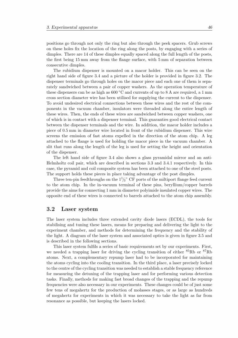
3. Experimental apparatus 46
positions go through not only the ring but also through the peek spacers. Grub screwson these holes fix the location of the ring along the posts, by engaging with a series ofdimples. There are 14 of these dimples equally spaced along the full length of the posts,the first being 15 mm away from the flange surface, with 5 mm of separation betweenconsecutive dimples.
The rubidium dispenser is mounted on a macor holder. This can be seen on theright hand side of figure 3.4 and a picture of the holder is provided in figure 3.2. Thedispenser terminals go through holes on the macor piece and each one of them is sepa-rately sandwiched between a pair of copper washers. As the operation temperature ofthese dispensers can be as high as 600 !C and currents of up to 8 A are required, a 1 mmcross section diameter wire has been utilised for supplying the current to the dispenser.To avoid undesired electrical connections between these wires and the rest of the com-ponents in the vacuum chamber, insulators were threaded along the entire length ofthese wires. Then, the ends of these wires are sandwiched between copper washers, oneof which is in contact with a dispenser terminal. This guaranties good electrical contactbetween the dispenser terminals and the wire. In addition, the macor holder includes apiece of 0.5 mm in diameter wire located in front of the rubidium dispenser. This wirescreens the emission of fast atoms expelled in the direction of the atom chip. A legattached to the flange is used for holding the macor piece in the vacuum chamber. Aslit that runs along the length of the leg is used for setting the height and orientationof the dispenser.
The left hand side of figure 3.4 also shows a glass pyramidal mirror and an anti-Helmholtz coil pair, which are described in sections 3.3 and 3.4.1 respectively. In thiscase, the pyramid and coil composite system has been attached to one of the steel posts.The support holds these pieces in place taking advantage of the post dimples.
Three ten-pin feedthroughs on the 11/3” CF ports of the miltiport flange feed currentto the atom chip. In the in-vacuum terminal of these pins, beryllium/copper barrelsprovide the aims for connecting 1 mm in diameter polyimide insulated copper wires. Theopposite end of these wires is connected to barrels attached to the atom chip assembly.
3.2 Laser system
The laser system includes three extended cavity diode lasers (ECDL), the tools forstabilising and tuning these lasers, means for preparing and delivering the light to theexperiment chamber, and methods for determining the frequency and the stability ofthe light. A diagram of the laser system and associated optics is given in figure 3.5 andis described in the following sections.
This laser system fulfils a series of basic requirements set by our experiments. First,we needed a trapping laser for driving the cycling transition of either 85Rb or 87Rbatoms. Next, a complementary repump laser had to be incorporated for maintainingthe atoms cycling into the cooling transition. In the third place, a laser precisely lockedto the centre of the cycling transition was needed to establish a stable frequency referencefor measuring the detuning of the trapping laser and for performing various detectiontasks. Finally, methods for making fast broad changes of the trapping and the repumpfrequencies were also necessary in our experiments. These changes could be of just somefew tens of megahertz for the production of molasses stages, or as large as hundredsof megahertz for experiments in which it was necessary to take the light as far fromresonance as possible, but keeping the lasers locked.
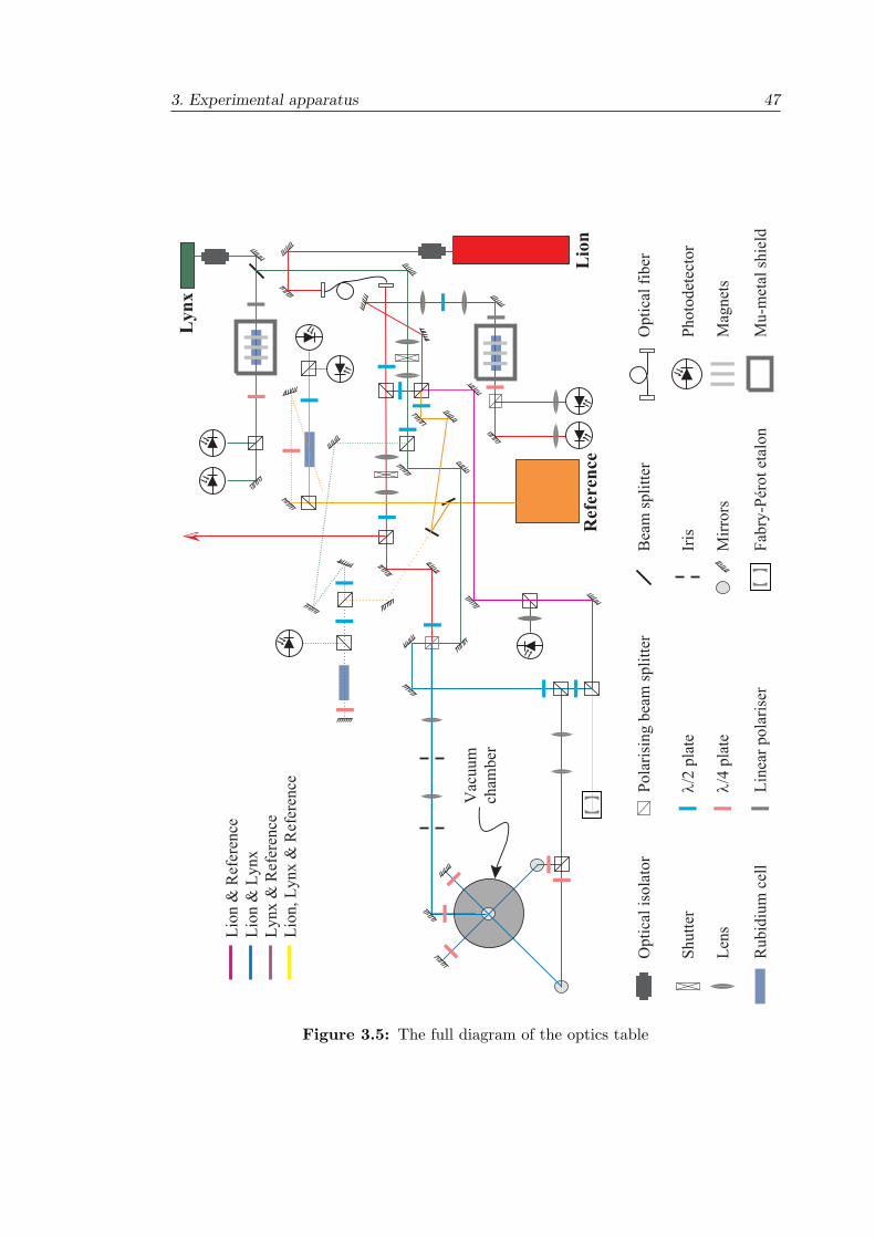
3. Experimental apparatus 47
Lion
Lynx
Reference
Lio
n &
Refe
rence
Lio
n &
Lynx
Lynx &
Refe
rence
Lio
n, L
ynx &
Refe
rence
Vacuum
cham
ber
Opti
cal
isola
tor
Shutt
er
Lens
Pola
risin
g b
eam
spli
tter
Photo
dete
cto
r
Mir
rors
Fabry
-Péro
t eta
lon
Rubid
ium
cell
Beam
spli
tter
Iris
/2 p
late
/4 p
late
Lin
ear
pola
riser
Magnets
Mu-m
eta
l shie
ld
Opti
cal
fiber
Figure 3.5: The full diagram of the optics table
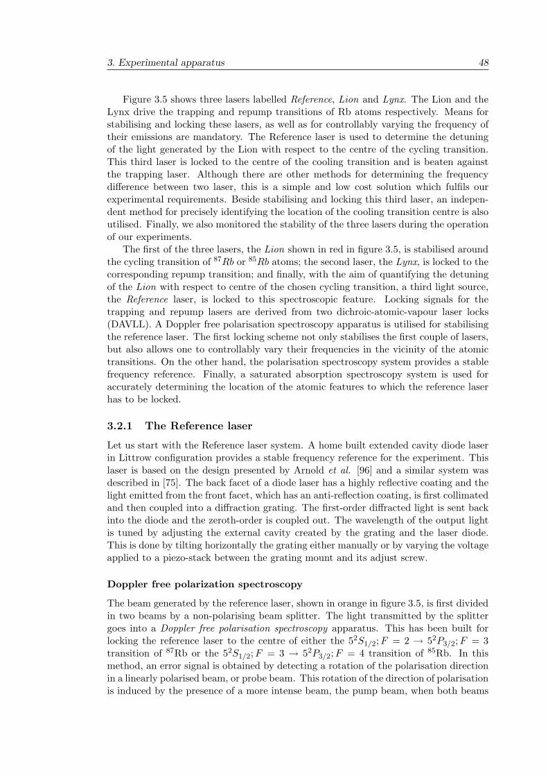
3. Experimental apparatus 48
Figure 3.5 shows three lasers labelled Reference, Lion and Lynx. The Lion and theLynx drive the trapping and repump transitions of Rb atoms respectively. Means forstabilising and locking these lasers, as well as for controllably varying the frequency oftheir emissions are mandatory. The Reference laser is used to determine the detuningof the light generated by the Lion with respect to the centre of the cycling transition.This third laser is locked to the centre of the cooling transition and is beaten againstthe trapping laser. Although there are other methods for determining the frequencydi"erence between two laser, this is a simple and low cost solution which fulfils ourexperimental requirements. Beside stabilising and locking this third laser, an indepen-dent method for precisely identifying the location of the cooling transition centre is alsoutilised. Finally, we also monitored the stability of the three lasers during the operationof our experiments.
The first of the three lasers, the Lion shown in red in figure 3.5, is stabilised aroundthe cycling transition of 87Rb or 85Rb atoms; the second laser, the Lynx, is locked to thecorresponding repump transition; and finally, with the aim of quantifying the detuningof the Lion with respect to centre of the chosen cycling transition, a third light source,the Reference laser, is locked to this spectroscopic feature. Locking signals for thetrapping and repump lasers are derived from two dichroic-atomic-vapour laser locks(DAVLL). A Doppler free polarisation spectroscopy apparatus is utilised for stabilisingthe reference laser. The first locking scheme not only stabilises the first couple of lasers,but also allows one to controllably vary their frequencies in the vicinity of the atomictransitions. On the other hand, the polarisation spectroscopy system provides a stablefrequency reference. Finally, a saturated absorption spectroscopy system is used foraccurately determining the location of the atomic features to which the reference laserhas to be locked.
3.2.1 The Reference laser
Let us start with the Reference laser system. A home built extended cavity diode laserin Littrow configuration provides a stable frequency reference for the experiment. Thislaser is based on the design presented by Arnold et al. [96] and a similar system wasdescribed in [75]. The back facet of a diode laser has a highly reflective coating and thelight emitted from the front facet, which has an anti-reflection coating, is first collimatedand then coupled into a di"raction grating. The first-order di"racted light is sent backinto the diode and the zeroth-order is coupled out. The wavelength of the output lightis tuned by adjusting the external cavity created by the grating and the laser diode.This is done by tilting horizontally the grating either manually or by varying the voltageapplied to a piezo-stack between the grating mount and its adjust screw.
Doppler free polarization spectroscopy
The beam generated by the reference laser, shown in orange in figure 3.5, is first dividedin two beams by a non-polarising beam splitter. The light transmitted by the splittergoes into a Doppler free polarisation spectroscopy apparatus. This has been built forlocking the reference laser to the centre of either the 52S1/2;F = 2 ( 52P3/2;F = 3transition of 87Rb or the 52S1/2;F = 3 ( 52P3/2;F = 4 transition of 85Rb. In thismethod, an error signal is obtained by detecting a rotation of the polarisation directionin a linearly polarised beam, or probe beam. This rotation of the direction of polarisationis induced by the presence of a more intense beam, the pump beam, when both beams
3. Experimental apparatus 49
/4
Rb PD1
PBS
PD2
/2
+
Figure 3.6: The Doppler-free polarisationspectroscopy system used for locking thereference laser to the two cycling transi-tions in the D2 line of both Rb isotopes.
-2.0 -1.5 -1.0 -0.5 0.0 0.5 1.0
-0.30
-0.15
0.00
0.15
Vol
tage
(a.u
.)
Frequency (GHz)
-0.10.00.10.20.3
B
A
85Rb87Rb
Figure 3.7: The error signal used for locking the reference lasers. GraphA shows the error signal obtained from the polarisation spectroscopy system,and graph B corresponds to the saturated absorption spectrum. The centreof the trapping transitions in 85Rb and 87Rb are identified on the saturatedabsorption spectrum and then used to lock the reference laser. These lockingpoints are identified by the vertical lines included in the figure.
are overlapped in an atomic vapour cell.The principle of polarisation spectroscopy is to induce a birefringence in a medium
with a circularly polarised pump beam and to interrogate this with a counterpropagatingweak probe beam [97]. Figure 3.6 shows the Doppler-free polarisation spectroscopysystem for locking the reference laser. First of all, the input beam is separated into twolinearly polarised components by a polarising beam cube. Before this cube, a "/2 plate(not shown in the figure) can be used to control the relative power of these two beams.
The beam transmitted by the beam cube is sent through a "/4 plate, which preparesthe circularly polarisation of the pump beam. This light beam is then sent througha rubidium cell. The probe beam, which is the beam reflected by the first cube, travelsthrough the rubidium vapour intersecting the pump beam inside the cell with the twobeams travelling nearly in opposite directions. Then, the birefringence induced by
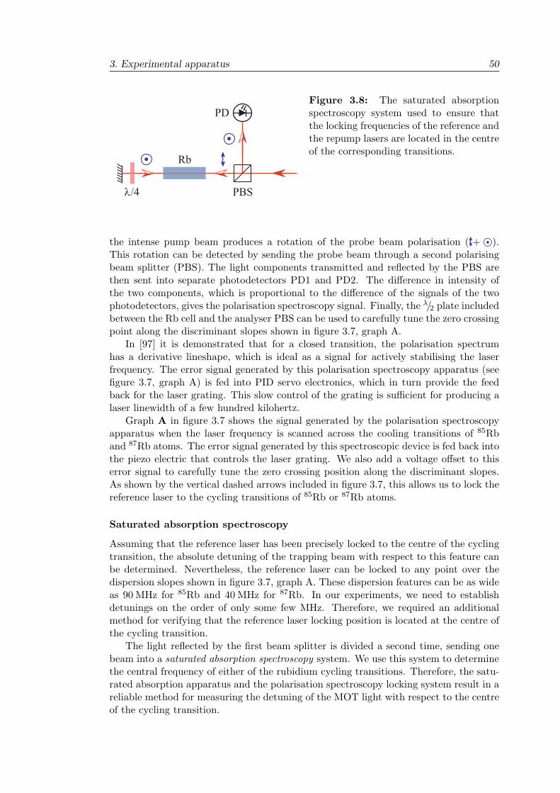
3. Experimental apparatus 50
/4
Rb
PD
PBS
Figure 3.8: The saturated absorptionspectroscopy system used to ensure thatthe locking frequencies of the reference andthe repump lasers are located in the centreof the corresponding transitions.
the intense pump beam produces a rotation of the probe beam polarisation ( + ).This rotation can be detected by sending the probe beam through a second polarisingbeam splitter (PBS). The light components transmitted and reflected by the PBS arethen sent into separate photodetectors PD1 and PD2. The di"erence in intensity ofthe two components, which is proportional to the di"erence of the signals of the twophotodetectors, gives the polarisation spectroscopy signal. Finally, the "/2 plate includedbetween the Rb cell and the analyser PBS can be used to carefully tune the zero crossingpoint along the discriminant slopes shown in figure 3.7, graph A.
In [97] it is demonstrated that for a closed transition, the polarisation spectrumhas a derivative lineshape, which is ideal as a signal for actively stabilising the laserfrequency. The error signal generated by this polarisation spectroscopy apparatus (seefigure 3.7, graph A) is fed into PID servo electronics, which in turn provide the feedback for the laser grating. This slow control of the grating is su!cient for producing alaser linewidth of a few hundred kilohertz.
Graph A in figure 3.7 shows the signal generated by the polarisation spectroscopyapparatus when the laser frequency is scanned across the cooling transitions of 85Rband 87Rb atoms. The error signal generated by this spectroscopic device is fed back intothe piezo electric that controls the laser grating. We also add a voltage o"set to thiserror signal to carefully tune the zero crossing position along the discriminant slopes.As shown by the vertical dashed arrows included in figure 3.7, this allows us to lock thereference laser to the cycling transitions of 85Rb or 87Rb atoms.
Saturated absorption spectroscopy
Assuming that the reference laser has been precisely locked to the centre of the cyclingtransition, the absolute detuning of the trapping beam with respect to this feature canbe determined. Nevertheless, the reference laser can be locked to any point over thedispersion slopes shown in figure 3.7, graph A. These dispersion features can be as wideas 90 MHz for 85Rb and 40 MHz for 87Rb. In our experiments, we need to establishdetunings on the order of only some few MHz. Therefore, we required an additionalmethod for verifying that the reference laser locking position is located at the centre ofthe cycling transition.
The light reflected by the first beam splitter is divided a second time, sending onebeam into a saturated absorption spectroscopy system. We use this system to determinethe central frequency of either of the rubidium cycling transitions. Therefore, the satu-rated absorption apparatus and the polarisation spectroscopy locking system result in areliable method for measuring the detuning of the MOT light with respect to the centreof the cycling transition.
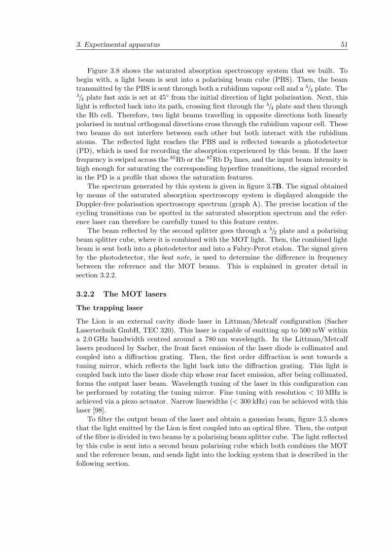
3. Experimental apparatus 51
Figure 3.8 shows the saturated absorption spectroscopy system that we built. Tobegin with, a light beam is sent into a polarising beam cube (PBS). Then, the beamtransmitted by the PBS is sent through both a rubidium vapour cell and a "/4 plate. The"/4 plate fast axis is set at 45! from the initial direction of light polarisation. Next, thislight is reflected back into its path, crossing first through the "/4 plate and then throughthe Rb cell. Therefore, two light beams travelling in opposite directions both linearlypolarised in mutual orthogonal directions cross through the rubidium vapour cell. Thesetwo beams do not interfere between each other but both interact with the rubidiumatoms. The reflected light reaches the PBS and is reflected towards a photodetector(PD), which is used for recording the absorption experienced by this beam. If the laserfrequency is swiped across the 85Rb or the 87Rb D2 lines, and the input beam intensity ishigh enough for saturating the corresponding hyperfine transitions, the signal recordedin the PD is a profile that shows the saturation features.
The spectrum generated by this system is given in figure 3.7B. The signal obtainedby means of the saturated absorption spectroscopy system is displayed alongside theDoppler-free polarisation spectroscopy spectrum (graph A). The precise location of thecycling transitions can be spotted in the saturated absorption spectrum and the refer-ence laser can therefore be carefully tuned to this feature centre.
The beam reflected by the second splitter goes through a "/2 plate and a polarisingbeam splitter cube, where it is combined with the MOT light. Then, the combined lightbeam is sent both into a photodetector and into a Fabry-Perot etalon. The signal givenby the photodetector, the beat note, is used to determine the di"erence in frequencybetween the reference and the MOT beams. This is explained in greater detail insection 3.2.2.
3.2.2 The MOT lasers
The trapping laser
The Lion is an external cavity diode laser in Littman/Metcalf configuration (SacherLasertechnik GmbH, TEC 320). This laser is capable of emitting up to 500 mW withina 2.0 GHz bandwidth centred around a 780 nm wavelength. In the Littman/Metcalflasers produced by Sacher, the front facet emission of the laser diode is collimated andcoupled into a di"raction grating. Then, the first order di"raction is sent towards atuning mirror, which reflects the light back into the di"raction grating. This light iscoupled back into the laser diode chip whose rear facet emission, after being collimated,forms the output laser beam. Wavelength tuning of the laser in this configuration canbe performed by rotating the tuning mirror. Fine tuning with resolution < 10 MHz isachieved via a piezo actuator. Narrow linewidths (< 300 kHz) can be achieved with thislaser [98].
To filter the output beam of the laser and obtain a gaussian beam, figure 3.5 showsthat the light emitted by the Lion is first coupled into an optical fibre. Then, the outputof the fibre is divided in two beams by a polarising beam splitter cube. The light reflectedby this cube is sent into a second beam polarising cube which both combines the MOTand the reference beam, and sends light into the locking system that is described in thefollowing section.
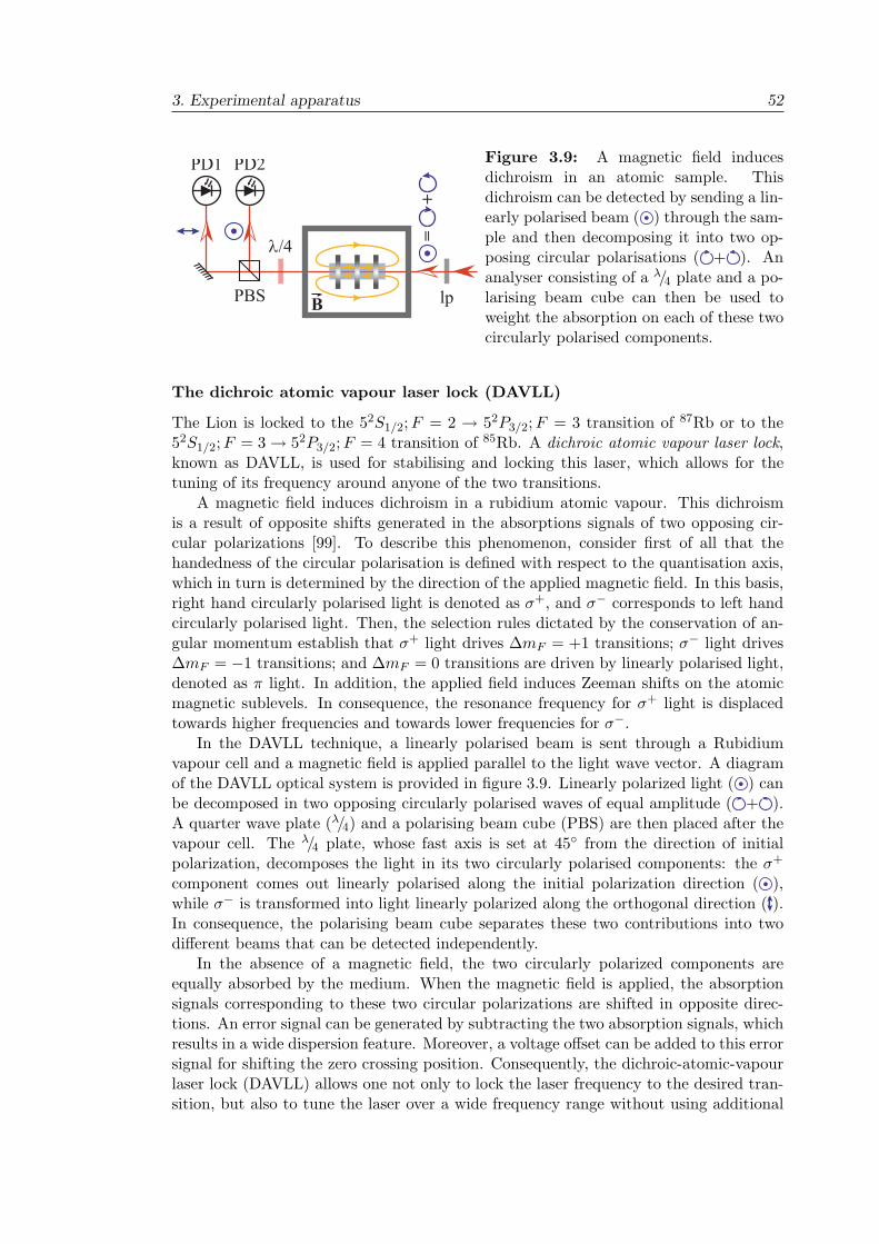
3. Experimental apparatus 52
PD2
/4
lp
PD1
BPBS
+
=
Figure 3.9: A magnetic field inducesdichroism in an atomic sample. Thisdichroism can be detected by sending a lin-early polarised beam ( ) through the sam-ple and then decomposing it into two op-posing circular polarisations ( + ). Ananalyser consisting of a "/4 plate and a po-larising beam cube can then be used toweight the absorption on each of these twocircularly polarised components.
The dichroic atomic vapour laser lock (DAVLL)
The Lion is locked to the 52S1/2;F = 2 ( 52P3/2;F = 3 transition of 87Rb or to the52S1/2;F = 3 ( 52P3/2;F = 4 transition of 85Rb. A dichroic atomic vapour laser lock,known as DAVLL, is used for stabilising and locking this laser, which allows for thetuning of its frequency around anyone of the two transitions.
A magnetic field induces dichroism in a rubidium atomic vapour. This dichroismis a result of opposite shifts generated in the absorptions signals of two opposing cir-cular polarizations [99]. To describe this phenomenon, consider first of all that thehandedness of the circular polarisation is defined with respect to the quantisation axis,which in turn is determined by the direction of the applied magnetic field. In this basis,right hand circularly polarised light is denoted as ,+, and ," corresponds to left handcircularly polarised light. Then, the selection rules dictated by the conservation of an-gular momentum establish that ,+ light drives $mF = +1 transitions; ," light drives$mF = "1 transitions; and $mF = 0 transitions are driven by linearly polarised light,denoted as & light. In addition, the applied field induces Zeeman shifts on the atomicmagnetic sublevels. In consequence, the resonance frequency for ,+ light is displacedtowards higher frequencies and towards lower frequencies for ,".
In the DAVLL technique, a linearly polarised beam is sent through a Rubidiumvapour cell and a magnetic field is applied parallel to the light wave vector. A diagramof the DAVLL optical system is provided in figure 3.9. Linearly polarized light ( ) canbe decomposed in two opposing circularly polarised waves of equal amplitude ( + ).A quarter wave plate ("/4) and a polarising beam cube (PBS) are then placed after thevapour cell. The "/4 plate, whose fast axis is set at 45! from the direction of initialpolarization, decomposes the light in its two circularly polarised components: the ,+
component comes out linearly polarised along the initial polarization direction ( ),while ," is transformed into light linearly polarized along the orthogonal direction ( ).In consequence, the polarising beam cube separates these two contributions into twodi"erent beams that can be detected independently.
In the absence of a magnetic field, the two circularly polarized components areequally absorbed by the medium. When the magnetic field is applied, the absorptionsignals corresponding to these two circular polarizations are shifted in opposite direc-tions. An error signal can be generated by subtracting the two absorption signals, whichresults in a wide dispersion feature. Moreover, a voltage o"set can be added to this errorsignal for shifting the zero crossing position. Consequently, the dichroic-atomic-vapourlaser lock (DAVLL) allows one not only to lock the laser frequency to the desired tran-sition, but also to tune the laser over a wide frequency range without using additional
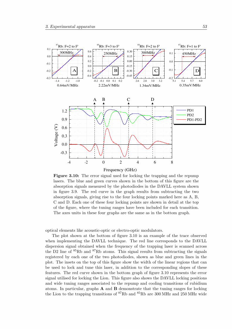
3. Experimental apparatus 53
-1.4 -1.2 -1.0-0.3
-0.2
-0.1
0.0
0.1
-0.2 -0.1 0.0 0.1 0.2
-0.4
-0.2
0.0
0.2
0.4
0.6
2.6 2.8 3.0 3.2
-0.45
-0.30
-0.15
0.00
0.15
0.30
5.1 5.4 5.7 6.0-0.2
-0.1
0.0
0.1
C B A D
450MHz300MHz250MHz300MHz
0.64mV/MHz
2.22mV/MHz
0.35mV/MHz1.34mV/MHz
85Rb: F=2 to F' 87Rb: F=1 to F' 85Rb: F=3 to F' 87Rb: F=2 to F'
-4 -2 0 2 4 6 8
-0.3
0.0
0.3
0.6
0.9
1.2
DCBA
PD1 PD2 PD1-PD2
Vol
tage
(V)
Frequency (GHz)Figure 3.10: The error signal used for locking the trapping and the repumplasers. The blue and green curves shown in the bottom of this figure are theabsorption signals measured by the photodiodes in the DAVLL system shownin figure 3.9. The red curve in the graph results from subtracting the twoabsorption signals, giving rise to the four locking points marked here as A, B,C and D. Each one of these four locking points are shown in detail at the topof the figure, where the tuning ranges have been included for each transition.The axes units in these four graphs are the same as in the bottom graph.
optical elements like acoustic-optic or electro-optic modulators.The plot shown at the bottom of figure 3.10 is an example of the trace observed
when implementing the DAVLL technique. The red line corresponds to the DAVLLdispersion signal obtained when the frequency of the trapping laser is scanned acrossthe D2 line of 85Rb and 87Rb atoms. This signal results from subtracting the signalsregistered by each one of the two photodiodes, shown as blue and green lines in theplot. The insets on the top of this figure show the width of the linear regions that canbe used to lock and tune this laser, in addition to the corresponding slopes of thesefeatures. The red curve shown in the bottom graph of figure 3.10 represents the errorsignal utilised for locking the Lion. This figure also shows the DAVLL locking positionsand wide tuning ranges associated to the repump and cooling transitions of rubidiumatoms. In particular, graphs A and B demonstrate that the tuning ranges for lockingthe Lion to the trapping transitions of 87Rb and 85Rb are 300 MHz and 250 MHz wide
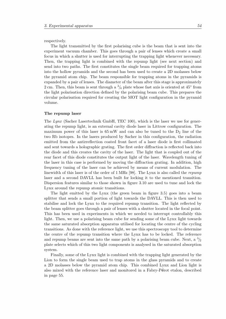
3. Experimental apparatus 54
respectively.The light transmitted by the first polarising cube is the beam that is sent into the
experiment vacuum chamber. This goes through a pair of lenses which create a smallfocus in which a shutter is used for interrupting the trapping light whenever necessary.Then, the trapping light is combined with the repump light (see next section) andsend into two paths. The first constitutes the single beam required for trapping atomsinto the hollow pyramids and the second has been used to create a 2D molasses belowthe pyramid atom chip. The beam responsible for trapping atoms in the pyramids isexpanded by a pair of lenses. The diameter of the beam after this stage is approximately2 cm. Then, this beam is sent through a "/4 plate whose fast axis is oriented at 45! fromthe light polarisation direction defined by the polarising beam cube. This prepares thecircular polarisation required for creating the MOT light configuration in the pyramidvolume.
The repump laser
The Lynx (Sacher Lasertechnik GmbH, TEC 100), which is the laser we use for gener-ating the repump light, is an external cavity diode laser in Littrow configuration. Themaximum power of this laser is 65 mW and can also be tuned to the D2 line of thetwo Rb isotopes. In the lasers produced by Sacher in this configuration, the radiationemitted from the antirreflection coated front facet of a laser diode is first collimatedand sent towards a holographic grating. The first order di"raction is reflected back intothe diode and this creates the cavity of the laser. The light that is coupled out of therear facet of this diode constitutes the output light of the laser. Wavelength tuning ofthe laser in this case is performed by moving the di"raction grating. In addition, highfrequency tuning of the laser can be achieved by means of current modulation. Thelinewidth of this laser is of the order of 1 MHz [98]. The Lynx is also called the repumplaser and a second DAVLL has been built for locking it to the mentioned transition.Dispersion features similar to those shown in figure 3.10 are used to tune and lock theLynx around the repump atomic transitions.
The light emitted by the Lynx (the green beam in figure 3.5) goes into a beamsplitter that sends a small portion of light towards the DAVLL. This is then used tostabilise and lock the Lynx to the required repump transition. The light reflected bythe beam splitter goes through a pair of lenses with a shutter located in the focal point.This has been used in experiments in which we needed to interrupt controllably thislight. Then, we use a polarising beam cube for sending some of the Lynx light towardsthe same saturated absorption apparatus utilised for locating the centre of the cyclingtransitions. As done with the reference light, we use this spectroscopy tool to determinethe centre of the repump transition where the Lynx has to be locked. The referenceand repump beams are sent into the same path by a polarising beam cube. Next, a "/2plate selects which of this two light components is analysed in the saturated absorptionsystem.
Finally, some of the Lynx light is combined with the trapping light generated by theLion to form the single beam used to trap atoms in the glass pyramids and to createa 2D molasses below the pyramid atom chip. This combined Lynx and Lion light isalso mixed with the reference laser and monitored in a Fabry-Perot etalon, describedin page 55.
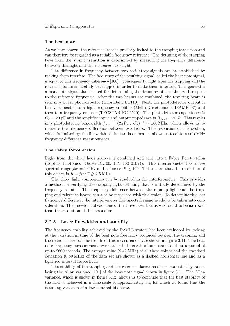
3. Experimental apparatus 55
The beat note
As we have shown, the reference laser is precisely locked to the trapping transition andcan therefore be regarded as a reliable frequency reference. The detuning of the trappinglaser from the atomic transition is determined by measuring the frequency di"erencebetween this light and the reference laser light.
The di"erence in frequency between two oscillatory signals can be established bymaking them interfere. The frequency of the resulting signal, called the beat note signal,is equal to this frequency di"erence [100]. Consequently, light from the trapping and thereference lasers is carefully overlapped in order to make them interfere. This generatesa beat note signal that is used for determining the detuning of the Lion with respectto the reference frequency. After the two beams are combined, the resulting beam issent into a fast photodetector (Thorlabs DET110). Next, the photodetector output isfirstly connected to a high frequency amplifier (Melles Griot, model 13AMP007) andthen to a frequency counter (TECSTAR FC 2500). The photodetector capacitance isCJ = 20 pF and the amplifier input and output impedance is RLoad = 50 &. This resultsin a photodetector bandwidth fBW = (2&RLoadCJ)"1 * 160 MHz, which allows us tomeasure the frequency di"erence between two lasers. The resolution of this system,which is limited by the linewidth of the two laser beams, allows us to obtain sub-MHzfrequency di"erence measurements.
The Fabry Perot etalon
Light from the three laser sources is combined and sent into a Fabry Perot etalon(Toptica Photonics. Series DL100, FPI 100 01094). This interferometer has a freespectral range fsr = 1 GHz and a finesse F " 400. This means that the resolution ofthis device is R = fsr/F " 2.5 MHz.
The three light components can be resolved in the interferometer. This providesa method for verifying the trapping light detuning that is initially determined by thefrequency counter. The frequency di"erence between the repump light and the trap-ping and reference beams can also be measured with this etalon. To determine this lastfrequency di"erence, the interferometer free spectral range needs to be taken into con-sideration. The linewidth of each one of the three laser beams was found to be narrowerthan the resolution of this resonator.
3.2.3 Laser linewidths and stability
The frequency stability achieved by the DAVLL system has been evaluated by lookingat the variation in time of the beat note frequency produced between the trapping andthe reference lasers. The results of this measurement are shown in figure 3.11. The beatnote frequency measurements were taken in intervals of one second and for a period ofup to 2600 seconds. The average value (9.42 MHz) of all these values and the standarddeviation (0.69 MHz) of the data set are shown as a dashed horizontal line and as alight red interval respectively.
The stability of the trapping and the reference lasers has been evaluated by calcu-lating the Allan variance [101] of the beat note signal shown in figure 3.11. The Allanvariance, which is shown in figure 3.12, allows us to conclude that the best stability ofthe laser is achieved in a time scale of approximately 3 s, for which we found that thedetuning variation of a few hundred kilohertz.
3. Experimental apparatus 56
Figure 3.11: The variation in time ofthe beat note signal generated by mixingthe trapping and the reference light beams.The beat note has been measured in in-tervals of one second and for a period of2600 seconds. The average value is shownas a dashed horizontal line and the stan-dard deviation of the detuning values ispresented as a light red interval around themean value.
Figure 3.12: The Allan variance of thebeat note signal presented in figure 3.11 ispresented in this figure. This analysis is ameasure of the stability of the two lasers,the Lion and the Reference, and has al-lowed to identify a random walk of thetrapping light frequency as the main sourceof noise.
Two di"erent methods have been utilised for measuring the linewidth of our lasers.First, in the optics plan given in figure 3.5 it is shown that light from the three lasers isshone into the Fabry Perot etalon. This way, each one of the three light components canbe monitored in real time. The resolution of this etalon has been shown to be limitedto ! 2.5 MHz, and the linewidth of the three lasers has been found to be consistentlybelow this limit. Secondly, the resolution with which we are capable of determiningthe detuning between the trapping and the reference light components is well below1 MHz. The linewidth of the beat note signal is the sum of the linewidths of the twooscillatory signals. Assuming that the linewidths of these two lasers are comparable, wecan conclude that these lasers are characterised by a linewidth of less than 500 kHz.
3.3 Large scale pyramidal mirrors
Two large-scale glass pyramids were fabricated for performing tests on the particulargeometry obtained when pyramidal pits are etched on a silicon surface. The first of
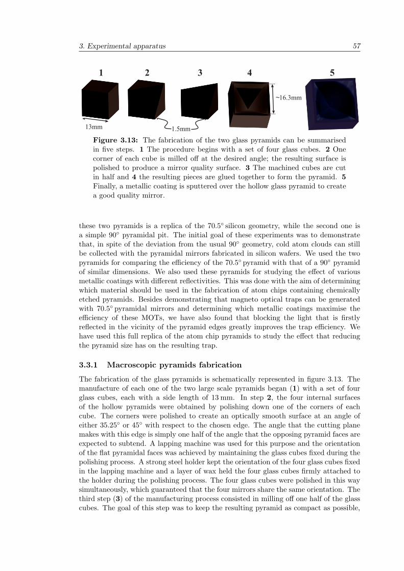
3. Experimental apparatus 57
1 2 3 4 5
13mm 1.5mm
16.3mm~
Figure 3.13: The fabrication of the two glass pyramids can be summarisedin five steps. 1 The procedure begins with a set of four glass cubes. 2 Onecorner of each cube is milled o" at the desired angle; the resulting surface ispolished to produce a mirror quality surface. 3 The machined cubes are cutin half and 4 the resulting pieces are glued together to form the pyramid. 5Finally, a metallic coating is sputtered over the hollow glass pyramid to createa good quality mirror.
these two pyramids is a replica of the 70.5! silicon geometry, while the second one isa simple 90! pyramidal pit. The initial goal of these experiments was to demonstratethat, in spite of the deviation from the usual 90! geometry, cold atom clouds can stillbe collected with the pyramidal mirrors fabricated in silicon wafers. We used the twopyramids for comparing the e!ciency of the 70.5! pyramid with that of a 90! pyramidof similar dimensions. We also used these pyramids for studying the e"ect of variousmetallic coatings with di"erent reflectivities. This was done with the aim of determiningwhich material should be used in the fabrication of atom chips containing chemicallyetched pyramids. Besides demonstrating that magneto optical traps can be generatedwith 70.5! pyramidal mirrors and determining which metallic coatings maximise thee!ciency of these MOTs, we have also found that blocking the light that is firstlyreflected in the vicinity of the pyramid edges greatly improves the trap e!ciency. Wehave used this full replica of the atom chip pyramids to study the e"ect that reducingthe pyramid size has on the resulting trap.
3.3.1 Macroscopic pyramids fabrication
The fabrication of the glass pyramids is schematically represented in figure 3.13. Themanufacture of each one of the two large scale pyramids began (1) with a set of fourglass cubes, each with a side length of 13 mm. In step 2, the four internal surfacesof the hollow pyramids were obtained by polishing down one of the corners of eachcube. The corners were polished to create an optically smooth surface at an angle ofeither 35.25! or 45! with respect to the chosen edge. The angle that the cutting planemakes with this edge is simply one half of the angle that the opposing pyramid faces areexpected to subtend. A lapping machine was used for this purpose and the orientationof the flat pyramidal faces was achieved by maintaining the glass cubes fixed during thepolishing process. A strong steel holder kept the orientation of the four glass cubes fixedin the lapping machine and a layer of wax held the four glass cubes firmly attached tothe holder during the polishing process. The four glass cubes were polished in this waysimultaneously, which guaranteed that the four mirrors share the same orientation. Thethird step (3) of the manufacturing process consisted in milling o" one half of the glasscubes. The goal of this step was to keep the resulting pyramid as compact as possible,
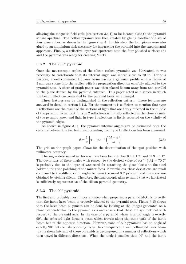
3. Experimental apparatus 58
allowing the magnetic field coils (see section 3.4.1) to be located close to the pyramidsquare aperture. The hollow pyramid was then created by gluing together the set offour glass cubes, as shown in the figure step 4. In this step, the four pieces were alsoglued to an aluminium disk necessary for integrating the pyramid into the experimentalapparatus. Finally, a reflective layer was sputtered onto the four polished surfaces (5)and the pyramid was ready for creating MOTs.
3.3.2 The 70.5! pyramid
Once the macroscopic replica of the silicon etched pyramids was fabricated, it wasnecessary to corroborate that its internal angle was indeed close to 70.5!. For thispurpose, a well collimated IR laser beam having a gaussian profile with a radius of5 mm was shone into the replica with its propagation direction carefully aligned to thepyramid axis. A sheet of graph paper was then placed 54 mm away from and parallelto the plane defined by the pyramid entrance. This paper acted as a screen in whichthe beam reflections generated by the pyramid faces were imaged.
Three features can be distinguished in the reflection pattern. These features areanalysed in detail in section 5.1.3. For the moment it is su!cient to mention that type1 reflections are the result of the sections of light that are firstly reflected in the middleof the pyramid faces; light in type 2 reflections is initially reflected in the close vicinityof the pyramid apex; and light in type 3 reflections is firstly reflected on the vicinity ofthe pyramid edges.
As shown in figure 3.14, the pyramid internal angles can be estimated once thedistance between the two features originating from type 1 reflections has been measured.
- =12
-& " tan"1
)M " a
2d
*.(3.3)
The grid on the graph paper allows for the determination of the spot position withmillimetre accuracy.
The angles determined in this way have been found to be 68.4 ± 1.7! and 67.9 ± 1.1!.The deviations of these angles with respect to the desired value of cos"1
11/3
2= 70.5!
is probably due to the layer of wax used for attaching the glass blocks to the steelholder during the polishing of the mirror faces. Nevertheless, these deviations are smallcompared to the di"erence in angles between the usual 90! pyramid and the structureobtained by etching silicon. Therefore, the macroscopic glass pyramid that we fabricatedis su!ciently representative of the silicon pyramid geometry.
3.3.3 The 90! pyramid
The first and probably most important step when preparing a pyramid MOT is to verifythat the input laser beam is properly aligned to the pyramid axis. Figure 3.15 showsthat the laser beam alignment can be done by looking at the images generated on aplane perpendicular to the pyramid axis and ensure that these are symmetrical withrespect to the pyramid axis. In the case of a pyramid whose internal angle is exactly90!, the reflected light forms a beam which travels along the same path of the inputbeam but in the opposite direction. However, none of our pyramids has an angle ofexactly 90! between its opposing faces. In consequence, a well collimated laser beamthat is shone into any of these pyramids is decomposed in a number of reflections whichthen travel in di"erent directions. When the angle is smaller than 90! and the input
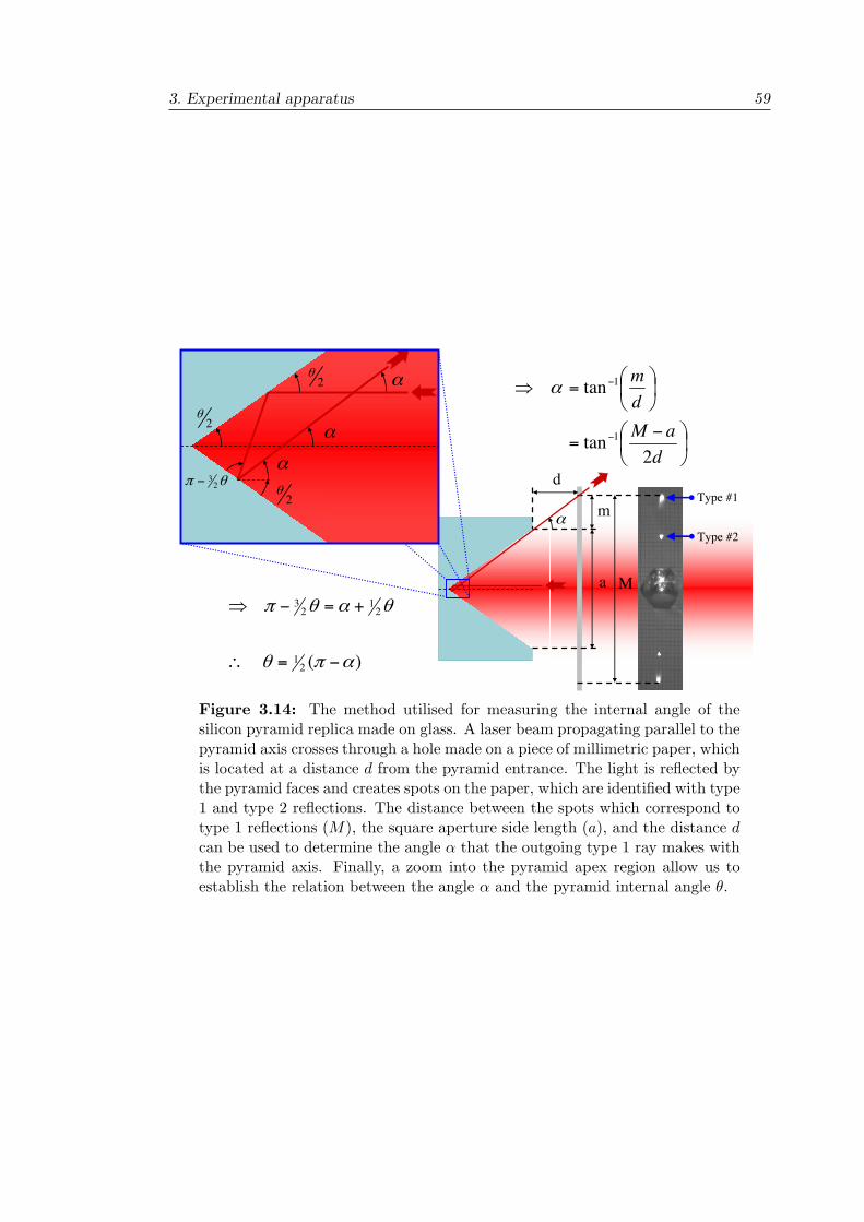
3. Experimental apparatus 59
α m
d
a M
Type #1
Type #2
α
2θ
θπ 23−
)(21
21
23
απθ
θαθπ
−=∴
+=−
2θ
2θ
α
α
−
=
=
−
−
daM
dm
2tan
tan
1
1α
Figure 3.14: The method utilised for measuring the internal angle of thesilicon pyramid replica made on glass. A laser beam propagating parallel to thepyramid axis crosses through a hole made on a piece of millimetric paper, whichis located at a distance d from the pyramid entrance. The light is reflected bythe pyramid faces and creates spots on the paper, which are identified with type1 and type 2 reflections. The distance between the spots which correspond totype 1 reflections (M), the square aperture side length (a), and the distance dcan be used to determine the angle $ that the outgoing type 1 ray makes withthe pyramid axis. Finally, a zoom into the pyramid apex region allow us toestablish the relation between the angle $ and the pyramid internal angle -.
3. Experimental apparatus 60
1 2 3 4 5 6
1
2
3
4
5
6
x (cm)
y (c
m)
Figure 3.15: A HeNe laser beam wasshone into the ! 90! pyramid and the re-flected light was imaged in a white paperscreen placed ! 20 cm away from the pyra-mid entrance. An image of the input beamhas been superimposed over the circularhole (white dashed line) on the screen.A schematic of the pyramid orientation isshown in grey. When the beam propa-gation direction is aligned to the pyramidaxis, the image formed in the screen is sym-metric with respect to this axis.
beam is properly aligned to the pyramid axis, the reflections generated by the pyramidsurfaces diverge symmetrically from the pyramid axis.
The internal angle of the nominally 90! pyramid was also determined following theprocedure described above. In this occasion, a HeNe laser beam was shone into thepyramid and a screen located approximately 20 cm away from the pyramid entrancewas used to image the reflection pattern shown in figure 3.15. This pyramid is 10 mmdeep and its aperture length is either 20.5 mm or 21.1 mm. The internal angles of thispyramid resulted to be 88.5! and 87.1! respectively.
3.3.4 Reflective coatings
Experiments in this thesis were done with a variety of reflective coatings. In a 70.5! pyramid,the trapping beam sections which are firstly reflected next to the edge of the pyramidfaces experience a total of three reflections before crossing through the pyramid axis,where atoms can be trapped. These light components produce an imbalance in the trap-ping force and unless attenuated or eliminated, the imbalance is su!cient for hinderingthe MOT functioning. Before crossing through the trapping region, these parasitic rayssu"er one more reflection on the pyramid surface than the rest of the trapping beam.Consequently, we proposed that the reflectivity of the mirror surface can be utilised forreducing the undesired e"ect of the parasitic light sections. In this thesis we have testedfour di"erent reflective coatings: aluminium, gold, platinum and chromium.
The information contained in table 3.1 provides the means for estimating the min-imum thickness of the metallic layer that should be achieved during the depositionprocess. The parameter 1/* ="/4!k, with $ being the absorption coe!cient, is knownas the skin depth. This parameter is a measure of how deep an electromagnetic wavewith wavelength % penetrates into a material whose extinction coe!cient is k:
1$
=%
4&k(3.4)
The first reflective coating used in both of our pyramids consisted of an aluminiumlayer covered by a magnesium fluoride (MgF2) protective layer. The reflectivity ofthis coating was determined by shining a HeNe laser beam onto each one of the fourpyramid mirror faces. The power of the incident beam was compared to the power of
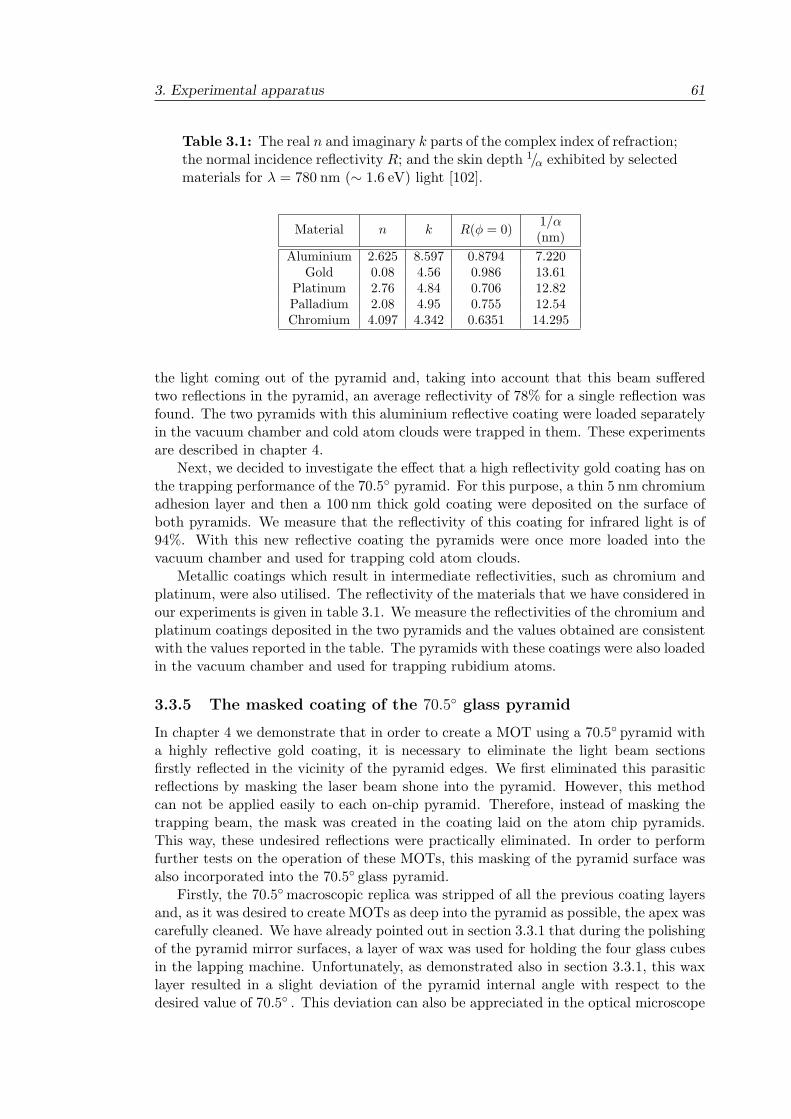
3. Experimental apparatus 61
Table 3.1: The real n and imaginary k parts of the complex index of refraction;the normal incidence reflectivity R; and the skin depth 1/* exhibited by selectedmaterials for % = 780 nm (! 1.6 eV) light [102].
Material n k R(/ = 0) 1/$(nm)
Aluminium 2.625 8.597 0.8794 7.220Gold 0.08 4.56 0.986 13.61
Platinum 2.76 4.84 0.706 12.82Palladium 2.08 4.95 0.755 12.54Chromium 4.097 4.342 0.6351 14.295
the light coming out of the pyramid and, taking into account that this beam su"eredtwo reflections in the pyramid, an average reflectivity of 78% for a single reflection wasfound. The two pyramids with this aluminium reflective coating were loaded separatelyin the vacuum chamber and cold atom clouds were trapped in them. These experimentsare described in chapter 4.
Next, we decided to investigate the e"ect that a high reflectivity gold coating has onthe trapping performance of the 70.5! pyramid. For this purpose, a thin 5 nm chromiumadhesion layer and then a 100 nm thick gold coating were deposited on the surface ofboth pyramids. We measure that the reflectivity of this coating for infrared light is of94%. With this new reflective coating the pyramids were once more loaded into thevacuum chamber and used for trapping cold atom clouds.
Metallic coatings which result in intermediate reflectivities, such as chromium andplatinum, were also utilised. The reflectivity of the materials that we have considered inour experiments is given in table 3.1. We measure the reflectivities of the chromium andplatinum coatings deposited in the two pyramids and the values obtained are consistentwith the values reported in the table. The pyramids with these coatings were also loadedin the vacuum chamber and used for trapping rubidium atoms.
3.3.5 The masked coating of the 70.5! glass pyramid
In chapter 4 we demonstrate that in order to create a MOT using a 70.5! pyramid witha highly reflective gold coating, it is necessary to eliminate the light beam sectionsfirstly reflected in the vicinity of the pyramid edges. We first eliminated this parasiticreflections by masking the laser beam shone into the pyramid. However, this methodcan not be applied easily to each on-chip pyramid. Therefore, instead of masking thetrapping beam, the mask was created in the coating laid on the atom chip pyramids.This way, these undesired reflections were practically eliminated. In order to performfurther tests on the operation of these MOTs, this masking of the pyramid surface wasalso incorporated into the 70.5! glass pyramid.
Firstly, the 70.5! macroscopic replica was stripped of all the previous coating layersand, as it was desired to create MOTs as deep into the pyramid as possible, the apex wascarefully cleaned. We have already pointed out in section 3.3.1 that during the polishingof the pyramid mirror surfaces, a layer of wax was used for holding the four glass cubesin the lapping machine. Unfortunately, as demonstrated also in section 3.3.1, this waxlayer resulted in a slight deviation of the pyramid internal angle with respect to thedesired value of 70.5! . This deviation can also be appreciated in the optical microscope
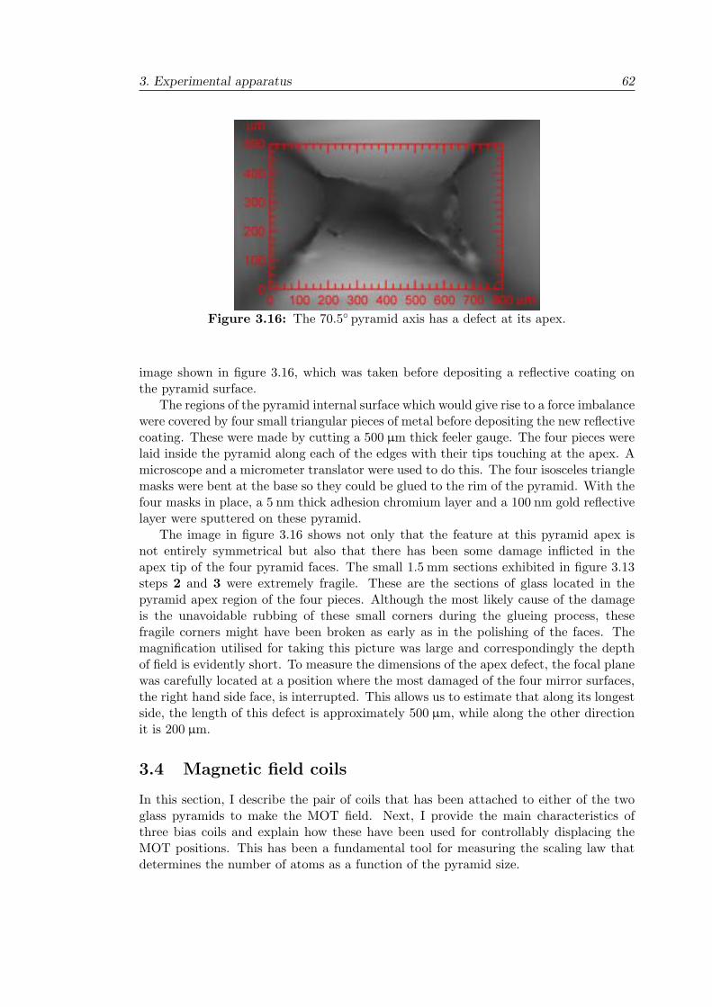
3. Experimental apparatus 62
Figure 3.16: The 70.5! pyramid axis has a defect at its apex.
image shown in figure 3.16, which was taken before depositing a reflective coating onthe pyramid surface.
The regions of the pyramid internal surface which would give rise to a force imbalancewere covered by four small triangular pieces of metal before depositing the new reflectivecoating. These were made by cutting a 500 µm thick feeler gauge. The four pieces werelaid inside the pyramid along each of the edges with their tips touching at the apex. Amicroscope and a micrometer translator were used to do this. The four isosceles trianglemasks were bent at the base so they could be glued to the rim of the pyramid. With thefour masks in place, a 5 nm thick adhesion chromium layer and a 100 nm gold reflectivelayer were sputtered on these pyramid.
The image in figure 3.16 shows not only that the feature at this pyramid apex isnot entirely symmetrical but also that there has been some damage inflicted in theapex tip of the four pyramid faces. The small 1.5 mm sections exhibited in figure 3.13steps 2 and 3 were extremely fragile. These are the sections of glass located in thepyramid apex region of the four pieces. Although the most likely cause of the damageis the unavoidable rubbing of these small corners during the glueing process, thesefragile corners might have been broken as early as in the polishing of the faces. Themagnification utilised for taking this picture was large and correspondingly the depthof field is evidently short. To measure the dimensions of the apex defect, the focal planewas carefully located at a position where the most damaged of the four mirror surfaces,the right hand side face, is interrupted. This allows us to estimate that along its longestside, the length of this defect is approximately 500 µm, while along the other directionit is 200 µm.
3.4 Magnetic field coils
In this section, I describe the pair of coils that has been attached to either of the twoglass pyramids to make the MOT field. Next, I provide the main characteristics ofthree bias coils and explain how these have been used for controllably displacing theMOT positions. This has been a fundamental tool for measuring the scaling law thatdetermines the number of atoms as a function of the pyramid size.
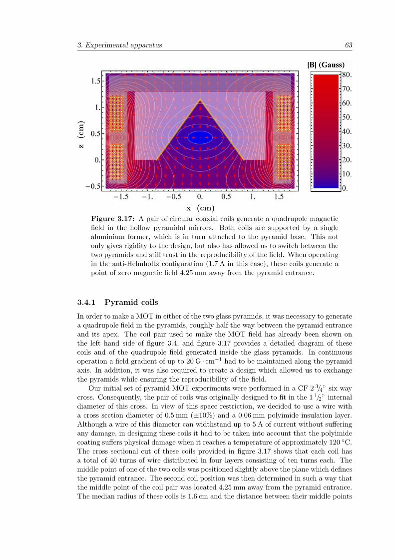
3. Experimental apparatus 63
z(c
m)
x (cm)Figure 3.17: A pair of circular coaxial coils generate a quadrupole magneticfield in the hollow pyramidal mirrors. Both coils are supported by a singlealuminium former, which is in turn attached to the pyramid base. This notonly gives rigidity to the design, but also has allowed us to switch between thetwo pyramids and still trust in the reproducibility of the field. When operatingin the anti-Helmholtz configuration (1.7 A in this case), these coils generate apoint of zero magnetic field 4.25 mm away from the pyramid entrance.
3.4.1 Pyramid coils
In order to make a MOT in either of the two glass pyramids, it was necessary to generatea quadrupole field in the pyramids, roughly half the way between the pyramid entranceand its apex. The coil pair used to make the MOT field has already been shown onthe left hand side of figure 3.4, and figure 3.17 provides a detailed diagram of thesecoils and of the quadrupole field generated inside the glass pyramids. In continuousoperation a field gradient of up to 20 G · cm"1 had to be maintained along the pyramidaxis. In addition, it was also required to create a design which allowed us to exchangethe pyramids while ensuring the reproducibility of the field.
Our initial set of pyramid MOT experiments were performed in a CF 2 3/4” six waycross. Consequently, the pair of coils was originally designed to fit in the 1 1/2” internaldiameter of this cross. In view of this space restriction, we decided to use a wire witha cross section diameter of 0.5 mm (±10%) and a 0.06 mm polyimide insulation layer.Although a wire of this diameter can widthstand up to 5 A of current without su"eringany damage, in designing these coils it had to be taken into account that the polyimidecoating su"ers physical damage when it reaches a temperature of approximately 120 !C.The cross sectional cut of these coils provided in figure 3.17 shows that each coil hasa total of 40 turns of wire distributed in four layers consisting of ten turns each. Themiddle point of one of the two coils was positioned slightly above the plane which definesthe pyramid entrance. The second coil position was then determined in such a way thatthe middle point of the coil pair was located 4.25 mm away from the pyramid entrance.The median radius of these coils is 1.6 cm and the distance between their middle points
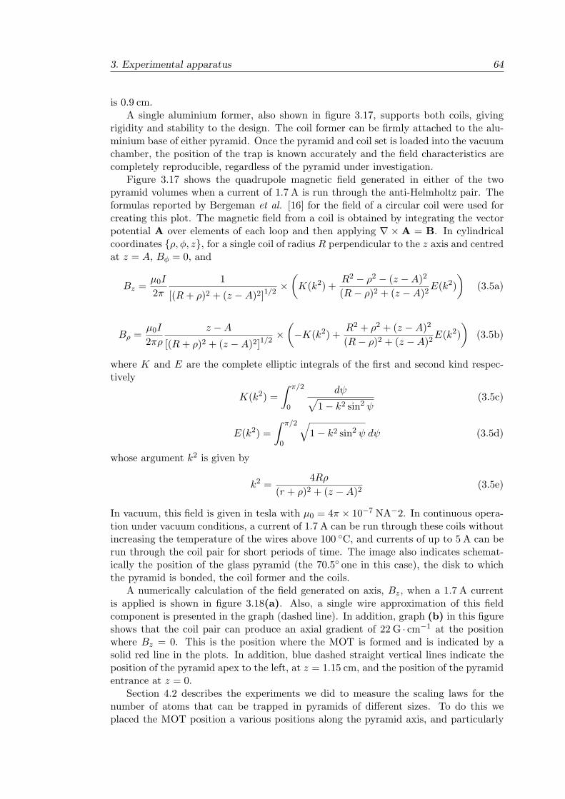
3. Experimental apparatus 64
is 0.9 cm.A single aluminium former, also shown in figure 3.17, supports both coils, giving
rigidity and stability to the design. The coil former can be firmly attached to the alu-minium base of either pyramid. Once the pyramid and coil set is loaded into the vacuumchamber, the position of the trap is known accurately and the field characteristics arecompletely reproducible, regardless of the pyramid under investigation.
Figure 3.17 shows the quadrupole magnetic field generated in either of the twopyramid volumes when a current of 1.7 A is run through the anti-Helmholtz pair. Theformulas reported by Bergeman et al. [16] for the field of a circular coil were used forcreating this plot. The magnetic field from a coil is obtained by integrating the vectorpotential A over elements of each loop and then applying - #A = B. In cylindricalcoordinates {0, /, z}, for a single coil of radius R perpendicular to the z axis and centredat z = A, B+ = 0, and
Bz =µ0I
2&
1[(R + 0)2 + (z "A)2]1/2
#)
K(k2) +R2 " 02 " (z "A)2
(R" 0)2 + (z "A)2E(k2)
*(3.5a)
B, =µ0I
2&0
z "A
[(R + 0)2 + (z "A)2]1/2#
)"K(k2) +
R2 + 02 + (z "A)2
(R" 0)2 + (z "A)2E(k2)
*(3.5b)
where K and E are the complete elliptic integrals of the first and second kind respec-tively
K(k2) =+ !/2
0
d1(1" k2 sin2 1
(3.5c)
E(k2) =+ !/2
0
31" k2 sin2 1 d1 (3.5d)
whose argument k2 is given by
k2 =4R0
(r + 0)2 + (z "A)2(3.5e)
In vacuum, this field is given in tesla with µ0 = 4& # 10"7 NA"2. In continuous opera-tion under vacuum conditions, a current of 1.7 A can be run through these coils withoutincreasing the temperature of the wires above 100 !C, and currents of up to 5 A can berun through the coil pair for short periods of time. The image also indicates schemat-ically the position of the glass pyramid (the 70.5! one in this case), the disk to whichthe pyramid is bonded, the coil former and the coils.
A numerically calculation of the field generated on axis, Bz, when a 1.7 A currentis applied is shown in figure 3.18(a). Also, a single wire approximation of this fieldcomponent is presented in the graph (dashed line). In addition, graph (b) in this figureshows that the coil pair can produce an axial gradient of 22 G · cm"1 at the positionwhere Bz = 0. This is the position where the MOT is formed and is indicated by asolid red line in the plots. In addition, blue dashed straight vertical lines indicate theposition of the pyramid apex to the left, at z = 1.15 cm, and the position of the pyramidentrance at z = 0.
Section 4.2 describes the experiments we did to measure the scaling laws for thenumber of atoms that can be trapped in pyramids of di"erent sizes. To do this weplaced the MOT position a various positions along the pyramid axis, and particularly
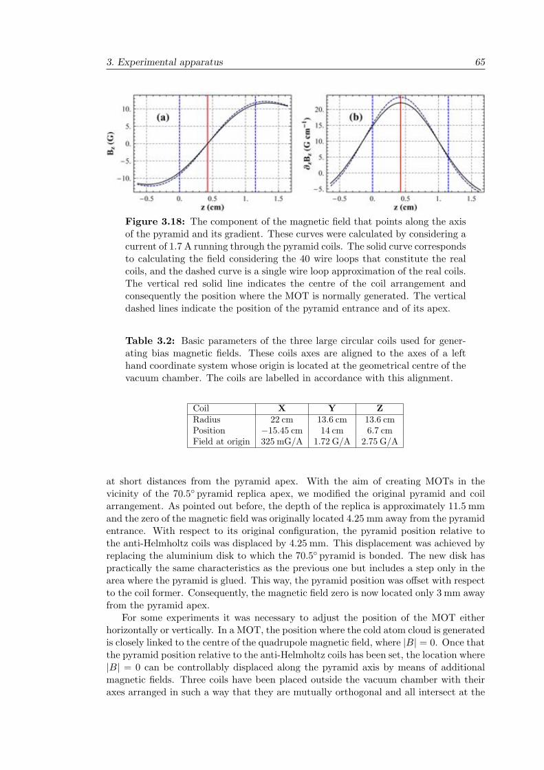
3. Experimental apparatus 65
Figure 3.18: The component of the magnetic field that points along the axisof the pyramid and its gradient. These curves were calculated by considering acurrent of 1.7 A running through the pyramid coils. The solid curve correspondsto calculating the field considering the 40 wire loops that constitute the realcoils, and the dashed curve is a single wire loop approximation of the real coils.The vertical red solid line indicates the centre of the coil arrangement andconsequently the position where the MOT is normally generated. The verticaldashed lines indicate the position of the pyramid entrance and of its apex.
Table 3.2: Basic parameters of the three large circular coils used for gener-ating bias magnetic fields. These coils axes are aligned to the axes of a lefthand coordinate system whose origin is located at the geometrical centre of thevacuum chamber. The coils are labelled in accordance with this alignment.
Coil X Y ZRadius 22 cm 13.6 cm 13.6 cmPosition "15.45 cm 14 cm 6.7 cmField at origin 325 mG/A 1.72 G/A 2.75 G/A
at short distances from the pyramid apex. With the aim of creating MOTs in thevicinity of the 70.5! pyramid replica apex, we modified the original pyramid and coilarrangement. As pointed out before, the depth of the replica is approximately 11.5 mmand the zero of the magnetic field was originally located 4.25 mm away from the pyramidentrance. With respect to its original configuration, the pyramid position relative tothe anti-Helmholtz coils was displaced by 4.25 mm. This displacement was achieved byreplacing the aluminium disk to which the 70.5! pyramid is bonded. The new disk haspractically the same characteristics as the previous one but includes a step only in thearea where the pyramid is glued. This way, the pyramid position was o"set with respectto the coil former. Consequently, the magnetic field zero is now located only 3 mm awayfrom the pyramid apex.
For some experiments it was necessary to adjust the position of the MOT eitherhorizontally or vertically. In a MOT, the position where the cold atom cloud is generatedis closely linked to the centre of the quadrupole magnetic field, where |B| = 0. Once thatthe pyramid position relative to the anti-Helmholtz coils has been set, the location where|B| = 0 can be controllably displaced along the pyramid axis by means of additionalmagnetic fields. Three coils have been placed outside the vacuum chamber with theiraxes arranged in such a way that they are mutually orthogonal and all intersect at the
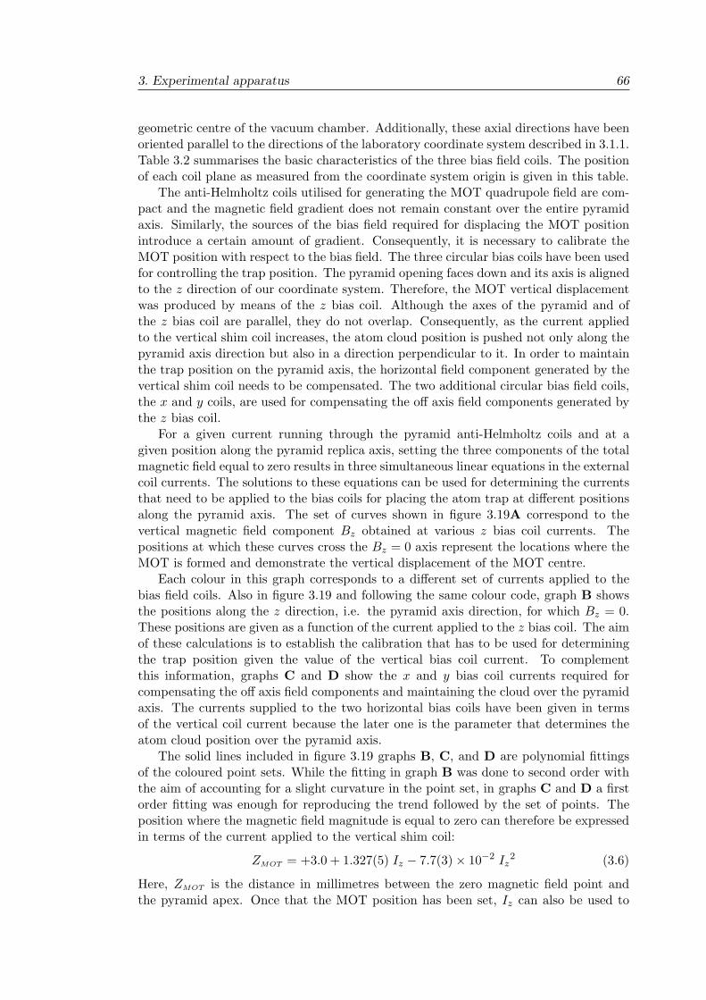
3. Experimental apparatus 66
geometric centre of the vacuum chamber. Additionally, these axial directions have beenoriented parallel to the directions of the laboratory coordinate system described in 3.1.1.Table 3.2 summarises the basic characteristics of the three bias field coils. The positionof each coil plane as measured from the coordinate system origin is given in this table.
The anti-Helmholtz coils utilised for generating the MOT quadrupole field are com-pact and the magnetic field gradient does not remain constant over the entire pyramidaxis. Similarly, the sources of the bias field required for displacing the MOT positionintroduce a certain amount of gradient. Consequently, it is necessary to calibrate theMOT position with respect to the bias field. The three circular bias coils have been usedfor controlling the trap position. The pyramid opening faces down and its axis is alignedto the z direction of our coordinate system. Therefore, the MOT vertical displacementwas produced by means of the z bias coil. Although the axes of the pyramid and ofthe z bias coil are parallel, they do not overlap. Consequently, as the current appliedto the vertical shim coil increases, the atom cloud position is pushed not only along thepyramid axis direction but also in a direction perpendicular to it. In order to maintainthe trap position on the pyramid axis, the horizontal field component generated by thevertical shim coil needs to be compensated. The two additional circular bias field coils,the x and y coils, are used for compensating the o" axis field components generated bythe z bias coil.
For a given current running through the pyramid anti-Helmholtz coils and at agiven position along the pyramid replica axis, setting the three components of the totalmagnetic field equal to zero results in three simultaneous linear equations in the externalcoil currents. The solutions to these equations can be used for determining the currentsthat need to be applied to the bias coils for placing the atom trap at di"erent positionsalong the pyramid axis. The set of curves shown in figure 3.19A correspond to thevertical magnetic field component Bz obtained at various z bias coil currents. Thepositions at which these curves cross the Bz = 0 axis represent the locations where theMOT is formed and demonstrate the vertical displacement of the MOT centre.
Each colour in this graph corresponds to a di"erent set of currents applied to thebias field coils. Also in figure 3.19 and following the same colour code, graph B showsthe positions along the z direction, i.e. the pyramid axis direction, for which Bz = 0.These positions are given as a function of the current applied to the z bias coil. The aimof these calculations is to establish the calibration that has to be used for determiningthe trap position given the value of the vertical bias coil current. To complementthis information, graphs C and D show the x and y bias coil currents required forcompensating the o" axis field components and maintaining the cloud over the pyramidaxis. The currents supplied to the two horizontal bias coils have been given in termsof the vertical coil current because the later one is the parameter that determines theatom cloud position over the pyramid axis.
The solid lines included in figure 3.19 graphs B, C, and D are polynomial fittingsof the coloured point sets. While the fitting in graph B was done to second order withthe aim of accounting for a slight curvature in the point set, in graphs C and D a firstorder fitting was enough for reproducing the trend followed by the set of points. Theposition where the magnetic field magnitude is equal to zero can therefore be expressedin terms of the current applied to the vertical shim coil:
ZMOT = +3.0 + 1.327(5) Iz " 7.7(3)# 10"2 Iz2 (3.6)
Here, ZMOT is the distance in millimetres between the zero magnetic field point andthe pyramid apex. Once that the MOT position has been set, Iz can also be used to
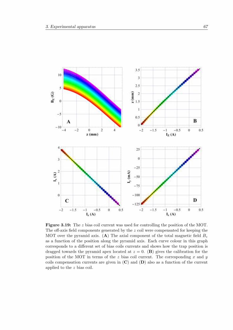
3. Experimental apparatus 67
Figure 3.19: The z bias coil current was used for controlling the position of the MOT.The o"-axis field components generated by the z coil were compensated for keeping theMOT over the pyramid axis. (A) The axial component of the total magnetic field Bz
as a function of the position along the pyramid axis. Each curve colour in this graphcorresponds to a di"erent set of bias coils currents and shows how the trap position isdragged towards the pyramid apex located at z = 0. (B) gives the calibration for theposition of the MOT in terms of the z bias coil current. The corresponding x and ycoils compensation currents are given in (C) and (D) also as a function of the currentapplied to the z bias coil.
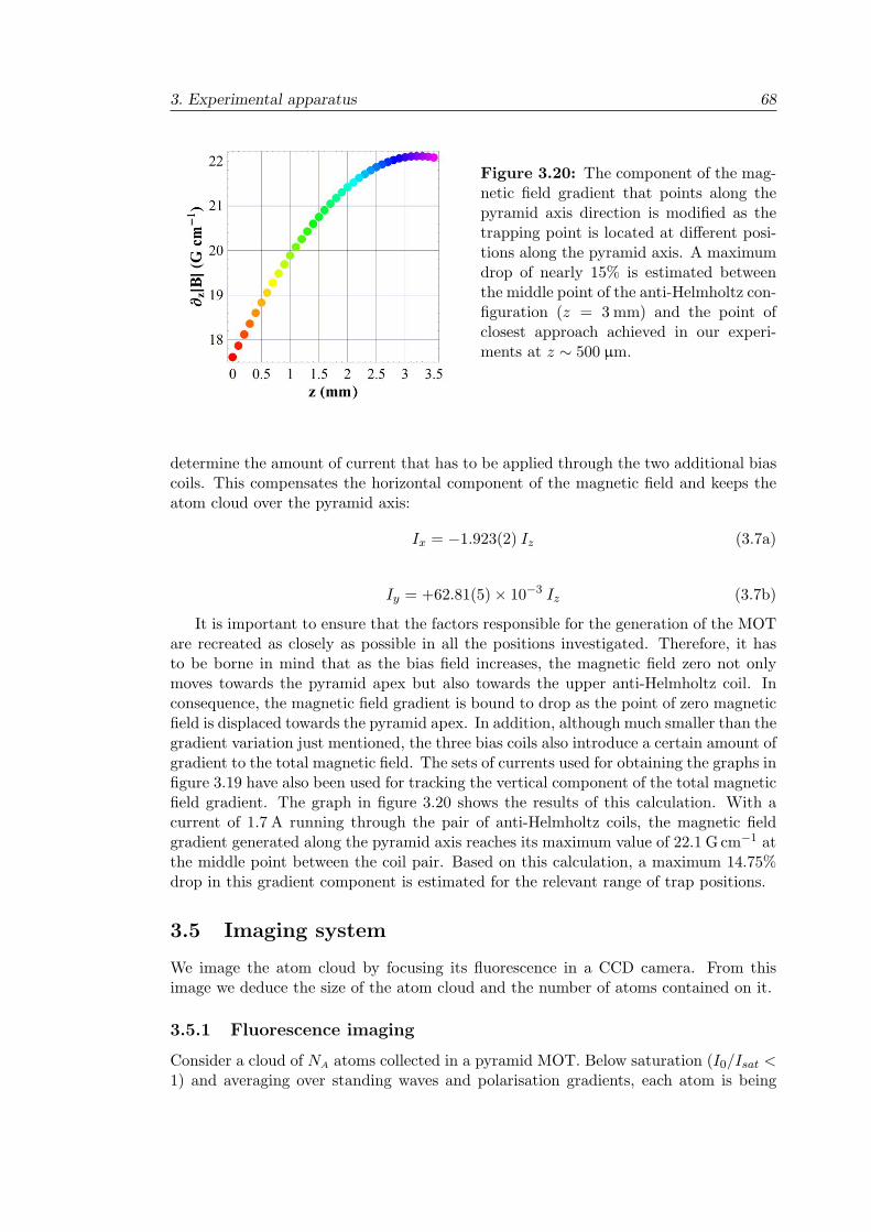
3. Experimental apparatus 68
Figure 3.20: The component of the mag-netic field gradient that points along thepyramid axis direction is modified as thetrapping point is located at di"erent posi-tions along the pyramid axis. A maximumdrop of nearly 15% is estimated betweenthe middle point of the anti-Helmholtz con-figuration (z = 3 mm) and the point ofclosest approach achieved in our experi-ments at z ! 500 µm.
determine the amount of current that has to be applied through the two additional biascoils. This compensates the horizontal component of the magnetic field and keeps theatom cloud over the pyramid axis:
Ix = "1.923(2) Iz (3.7a)
Iy = +62.81(5)# 10"3 Iz (3.7b)
It is important to ensure that the factors responsible for the generation of the MOTare recreated as closely as possible in all the positions investigated. Therefore, it hasto be borne in mind that as the bias field increases, the magnetic field zero not onlymoves towards the pyramid apex but also towards the upper anti-Helmholtz coil. Inconsequence, the magnetic field gradient is bound to drop as the point of zero magneticfield is displaced towards the pyramid apex. In addition, although much smaller than thegradient variation just mentioned, the three bias coils also introduce a certain amount ofgradient to the total magnetic field. The sets of currents used for obtaining the graphs infigure 3.19 have also been used for tracking the vertical component of the total magneticfield gradient. The graph in figure 3.20 shows the results of this calculation. With acurrent of 1.7 A running through the pair of anti-Helmholtz coils, the magnetic fieldgradient generated along the pyramid axis reaches its maximum value of 22.1 G cm"1 atthe middle point between the coil pair. Based on this calculation, a maximum 14.75%drop in this gradient component is estimated for the relevant range of trap positions.
3.5 Imaging system
We image the atom cloud by focusing its fluorescence in a CCD camera. From thisimage we deduce the size of the atom cloud and the number of atoms contained on it.
3.5.1 Fluorescence imaging
Consider a cloud of NA atoms collected in a pyramid MOT. Below saturation (I0/Isat <1) and averaging over standing waves and polarisation gradients, each atom is being
3. Experimental apparatus 69
continuously excited by the trapping light and therefore is emitting photons at a rate
R =#2
'I0/Isat
1 + 'I0/Isat + (2$-/#-)2. (3.8)
The factor ' accounts for all the di"erent light contributions interacting with the atom.In a MOT formed by six beams of equal intensity, this factor would be equal to 6. Ina perfect 90! pyramidal mirror with reflectivity 0, ' would be equal to (1 + 40 + 02).Finally, in a 70.5! pyramid also characterised by a reflectivity 0, ' = (1 + 40 + 402).
Each radiated photon carries an energy hc/". Hence, the energy radiated per atomper unit time is R hc/". Consider a CCD camera located at a distance D from the cloudcentre, whose lens defines an aperture diameter d. Then, for D . d, the solid anglesubtended by the camera lens is:
d& =&d2
4D2,
The detection e!ciency . of the camera, in counts/Joule, is required for relating thenumber of atoms NA collected in the cloud with the total number of counts NC in aMOT image. Via this e!ciency, the energy emitted by the atom cloud in the directionof the solid angle subtended by the camera produces an image with
NC = NARhc
%
d&4&
."e.
where "e is the exposure time of the camera. In conclusion, if the e!ciency of the CCDchip is known, the number of atoms collected in the cloud can be determined by meansof the following relation:
NA = NC
%
Rhc
4&
d&1
."e. (3.9)
Camera calibration
Three di"erent cameras have been utilised in our experiments. An AVT Marlin (AL-LIED Vision Technologies) is a particularly representative example of these cameras.As this is the camera that we have used in our latest experiments, we will limit ourselvesin this section to explaining the calibration method for this camera. Nevertheless, thisprocedure is completely generic and, with minor modifications, it has been applied forcalibrating the other cameras.
The calibration of the CCD camera consists of determining its e!ciency ., whichis the number of counts stored in a given pixel per unit of energy landing on it. Twoparameters influence the operation of the AVT camera, the shutter speed S and thegain G. These two parameters are set by the computer that controls the CCD camera.Although the exposure time is proportional to the shutter speed, "e / S, the factor ofproportionality is determined by the camera electronics and is not known. Because ofthis, we were not able to determine directly the e!ciency . of the camera. Instead, weperformed a counts to power calibration. Therefore, if the total number of pixel countsstored in an image is NC, the calibration of the camera should allow us to determinethe corresponding total amount of power detected by our imaging system.
The camera calibration procedure consisted of taking an image of a laser beam ofknown power that is shone directly into the CCD chip. This is repeated for severalcombinations of shutter speed, gain, and laser powers. During this process, care mustbe taken to ensure that the entire laser beam profile fits into the CCD chip area. Next,
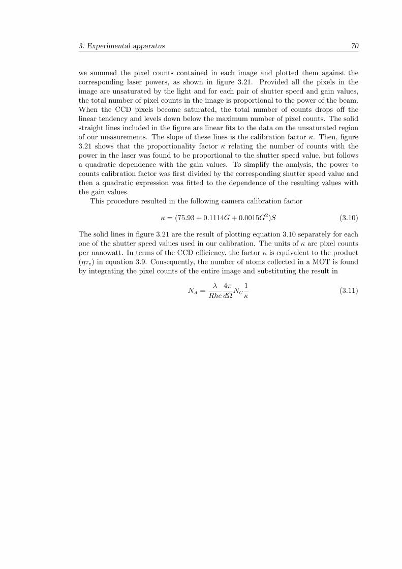
3. Experimental apparatus 70
we summed the pixel counts contained in each image and plotted them against thecorresponding laser powers, as shown in figure 3.21. Provided all the pixels in theimage are unsaturated by the light and for each pair of shutter speed and gain values,the total number of pixel counts in the image is proportional to the power of the beam.When the CCD pixels become saturated, the total number of counts drops o" thelinear tendency and levels down below the maximum number of pixel counts. The solidstraight lines included in the figure are linear fits to the data on the unsaturated regionof our measurements. The slope of these lines is the calibration factor !. Then, figure3.21 shows that the proportionality factor ! relating the number of counts with thepower in the laser was found to be proportional to the shutter speed value, but followsa quadratic dependence with the gain values. To simplify the analysis, the power tocounts calibration factor was first divided by the corresponding shutter speed value andthen a quadratic expression was fitted to the dependence of the resulting values withthe gain values.
This procedure resulted in the following camera calibration factor
! = (75.93 + 0.1114G + 0.0015G2)S (3.10)
The solid lines in figure 3.21 are the result of plotting equation 3.10 separately for eachone of the shutter speed values used in our calibration. The units of ! are pixel countsper nanowatt. In terms of the CCD e!ciency, the factor ! is equivalent to the product(."e) in equation 3.9. Consequently, the number of atoms collected in a MOT is foundby integrating the pixel counts of the entire image and substituting the result in
NA =%
Rhc
4&
d&NC
1!
(3.11)
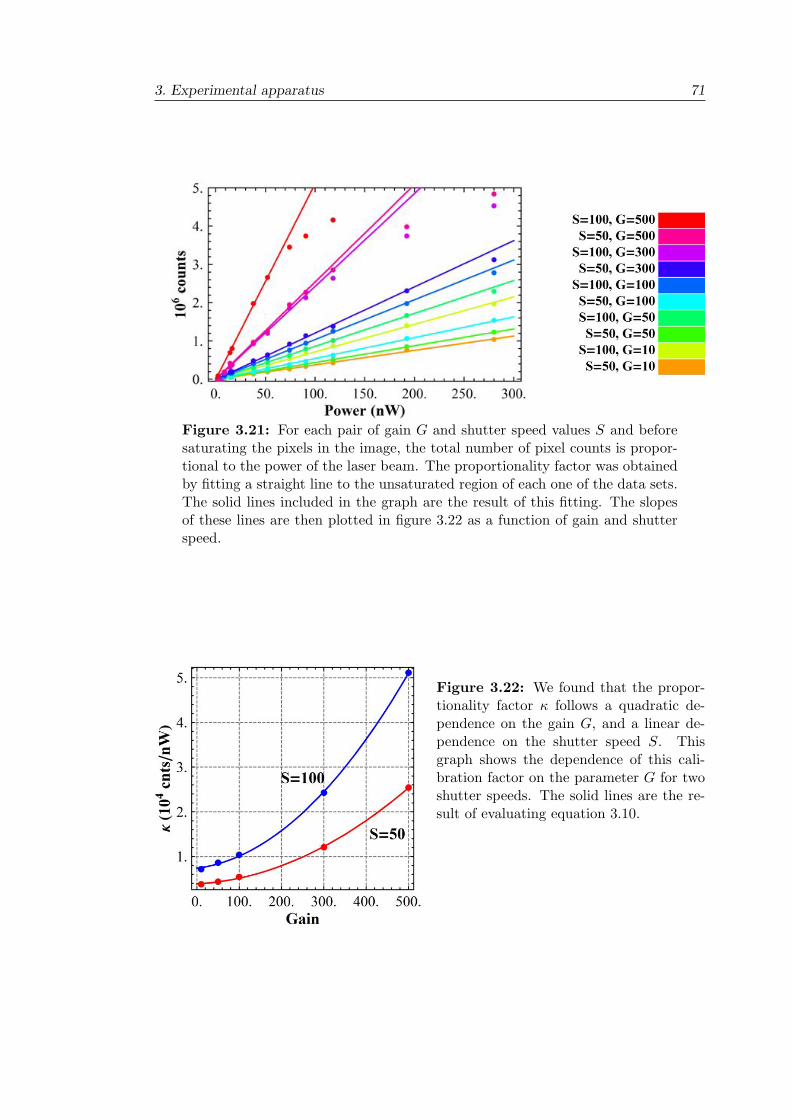
3. Experimental apparatus 71
Figure 3.21: For each pair of gain G and shutter speed values S and beforesaturating the pixels in the image, the total number of pixel counts is propor-tional to the power of the laser beam. The proportionality factor was obtainedby fitting a straight line to the unsaturated region of each one of the data sets.The solid lines included in the graph are the result of this fitting. The slopesof these lines are then plotted in figure 3.22 as a function of gain and shutterspeed.
Figure 3.22: We found that the propor-tionality factor ! follows a quadratic de-pendence on the gain G, and a linear de-pendence on the shutter speed S. Thisgraph shows the dependence of this cali-bration factor on the parameter G for twoshutter speeds. The solid lines are the re-sult of evaluating equation 3.10.
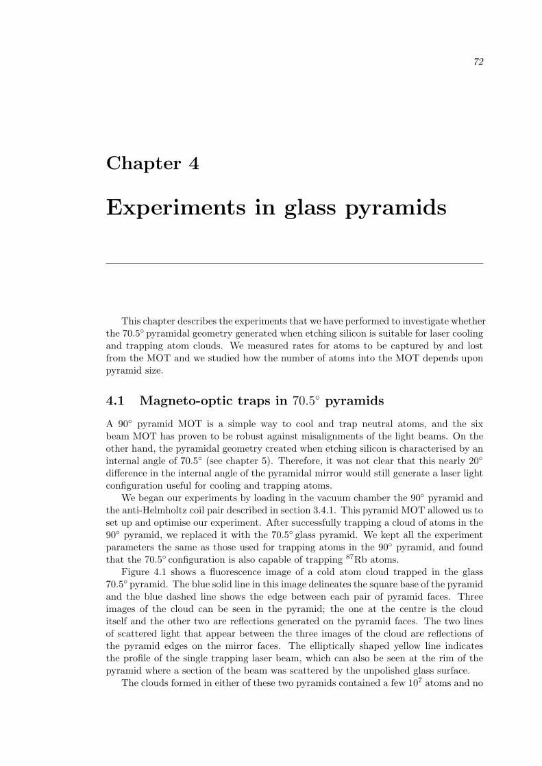
72
Chapter 4
Experiments in glass pyramids
This chapter describes the experiments that we have performed to investigate whetherthe 70.5! pyramidal geometry generated when etching silicon is suitable for laser coolingand trapping atom clouds. We measured rates for atoms to be captured by and lostfrom the MOT and we studied how the number of atoms into the MOT depends uponpyramid size.
4.1 Magneto-optic traps in 70.50 pyramids
A 90! pyramid MOT is a simple way to cool and trap neutral atoms, and the sixbeam MOT has proven to be robust against misalignments of the light beams. On theother hand, the pyramidal geometry created when etching silicon is characterised by aninternal angle of 70.5! (see chapter 5). Therefore, it was not clear that this nearly 20!
di"erence in the internal angle of the pyramidal mirror would still generate a laser lightconfiguration useful for cooling and trapping atoms.
We began our experiments by loading in the vacuum chamber the 90! pyramid andthe anti-Helmholtz coil pair described in section 3.4.1. This pyramid MOT allowed us toset up and optimise our experiment. After successfully trapping a cloud of atoms in the90! pyramid, we replaced it with the 70.5! glass pyramid. We kept all the experimentparameters the same as those used for trapping atoms in the 90! pyramid, and foundthat the 70.5! configuration is also capable of trapping 87Rb atoms.
Figure 4.1 shows a fluorescence image of a cold atom cloud trapped in the glass70.5! pyramid. The blue solid line in this image delineates the square base of the pyramidand the blue dashed line shows the edge between each pair of pyramid faces. Threeimages of the cloud can be seen in the pyramid; the one at the centre is the clouditself and the other two are reflections generated on the pyramid faces. The two linesof scattered light that appear between the three images of the cloud are reflections ofthe pyramid edges on the mirror faces. The elliptically shaped yellow line indicatesthe profile of the single trapping laser beam, which can also be seen at the rim of thepyramid where a section of the beam was scattered by the unpolished glass surface.
The clouds formed in either of these two pyramids contained a few 107 atoms and no
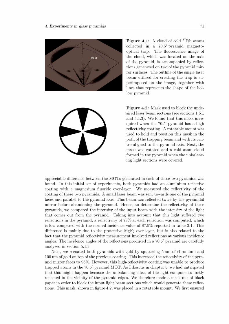
4. Experiments in glass pyramids 73
MOT
Figure 4.1: A cloud of cold 87Rb atomscollected in a 70.5! pyramid magneto-optical trap. The fluorescence image ofthe cloud, which was located on the axisof the pyramid, is accompanied by reflec-tions generated on two of the pyramid mir-ror surfaces. The outline of the single laserbeam utilised for creating the trap is su-perimposed on the image, together withlines that represents the shape of the hol-low pyramid.
Figure 4.2: Mask used to block the unde-sired laser beam sections (see sections 1.5.1and 5.1.3). We found that this mask is re-quired when the 70.5! pyramid has a highreflectivity coating. A rotatable mount wasused to hold and position this mask in thepath of the trapping beam and with its cen-tre aligned to the pyramid axis. Next, themask was rotated and a cold atom cloudformed in the pyramid when the unbalanc-ing light sections were covered.
appreciable di"erence between the MOTs generated in each of these two pyramids wasfound. In this initial set of experiments, both pyramids had an aluminium reflectivecoating with a magnesium fluoride over-layer. We measured the reflectivity of thecoating of these two pyramids. A small laser beam was sent towards one of the pyramidfaces and parallel to the pyramid axis. This beam was reflected twice by the pyramidalmirror before abandoning the pyramid. Hence, to determine the reflectivity of thesepyramids, we compared the intensity of the input beam with the intensity of the lightthat comes out from the pyramid. Taking into account that this light su"ered tworeflections in the pyramid, a reflectivity of 78% at each reflection was computed, whichis low compared with the normal incidence value of 87.9% reported in table 3.1. Thisdi"erence is mainly due to the protective MgF2 over-layer, but is also related to thefact that the pyramid reflectivity measurement involved reflections at various incidenceangles. The incidence angles of the reflections produced in a 70.5! pyramid are carefullyanalysed in section 5.1.3.
Next, we recoated both pyramids with gold by sputtering 5 nm of chromium and100 nm of gold on top of the previous coating. This increased the reflectivity of the pyra-mid mirror faces to 95%. However, this high-reflectivity coating was unable to producetrapped atoms in the 70.5! pyramid MOT. As I disscus in chapter 5, we had anticipatedthat this might happen because the unbalancing e"ect of the light components firstlyreflected in the vicinity of the pyramid edges. We therefore made a mask out of blackpaper in order to block the input light beam sections which would generate these reflec-tions. This mask, shown in figure 4.2, was placed in a rotatable mount. We first ensured
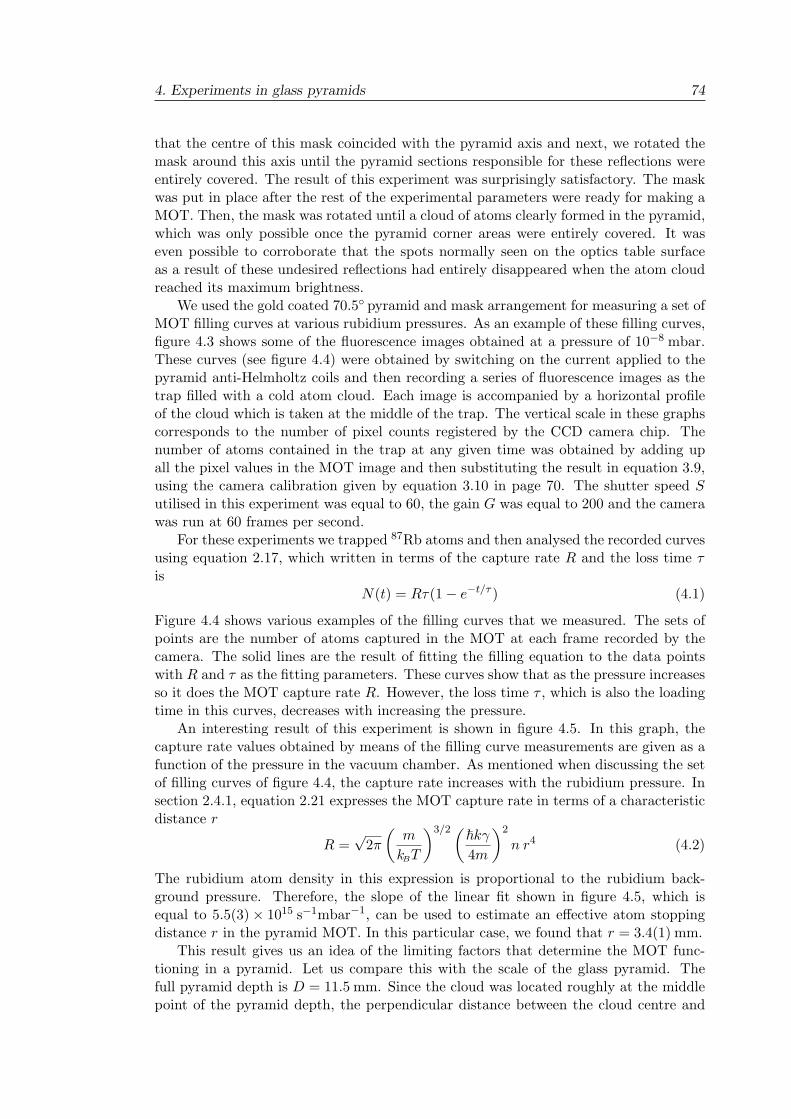
4. Experiments in glass pyramids 74
that the centre of this mask coincided with the pyramid axis and next, we rotated themask around this axis until the pyramid sections responsible for these reflections wereentirely covered. The result of this experiment was surprisingly satisfactory. The maskwas put in place after the rest of the experimental parameters were ready for making aMOT. Then, the mask was rotated until a cloud of atoms clearly formed in the pyramid,which was only possible once the pyramid corner areas were entirely covered. It waseven possible to corroborate that the spots normally seen on the optics table surfaceas a result of these undesired reflections had entirely disappeared when the atom cloudreached its maximum brightness.
We used the gold coated 70.5! pyramid and mask arrangement for measuring a set ofMOT filling curves at various rubidium pressures. As an example of these filling curves,figure 4.3 shows some of the fluorescence images obtained at a pressure of 10"8 mbar.These curves (see figure 4.4) were obtained by switching on the current applied to thepyramid anti-Helmholtz coils and then recording a series of fluorescence images as thetrap filled with a cold atom cloud. Each image is accompanied by a horizontal profileof the cloud which is taken at the middle of the trap. The vertical scale in these graphscorresponds to the number of pixel counts registered by the CCD camera chip. Thenumber of atoms contained in the trap at any given time was obtained by adding upall the pixel values in the MOT image and then substituting the result in equation 3.9,using the camera calibration given by equation 3.10 in page 70. The shutter speed Sutilised in this experiment was equal to 60, the gain G was equal to 200 and the camerawas run at 60 frames per second.
For these experiments we trapped 87Rb atoms and then analysed the recorded curvesusing equation 2.17, which written in terms of the capture rate R and the loss time "is
N(t) = R"(1" e"t/) ) (4.1)
Figure 4.4 shows various examples of the filling curves that we measured. The sets ofpoints are the number of atoms captured in the MOT at each frame recorded by thecamera. The solid lines are the result of fitting the filling equation to the data pointswith R and " as the fitting parameters. These curves show that as the pressure increasesso it does the MOT capture rate R. However, the loss time " , which is also the loadingtime in this curves, decreases with increasing the pressure.
An interesting result of this experiment is shown in figure 4.5. In this graph, thecapture rate values obtained by means of the filling curve measurements are given as afunction of the pressure in the vacuum chamber. As mentioned when discussing the setof filling curves of figure 4.4, the capture rate increases with the rubidium pressure. Insection 2.4.1, equation 2.21 expresses the MOT capture rate in terms of a characteristicdistance r
R =%
2&
)m
kBT
*3/2 )!k(
4m
*2
n r4 (4.2)
The rubidium atom density in this expression is proportional to the rubidium back-ground pressure. Therefore, the slope of the linear fit shown in figure 4.5, which isequal to 5.5(3)# 1015 s"1mbar"1, can be used to estimate an e"ective atom stoppingdistance r in the pyramid MOT. In this particular case, we found that r = 3.4(1) mm.
This result gives us an idea of the limiting factors that determine the MOT func-tioning in a pyramid. Let us compare this with the scale of the glass pyramid. Thefull pyramid depth is D = 11.5 mm. Since the cloud was located roughly at the middlepoint of the pyramid depth, the perpendicular distance between the cloud centre and
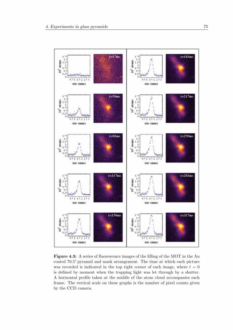
4. Experiments in glass pyramids 75
Figure 4.3: A series of fluorescence images of the filling of the MOT in the Aucoated 70.5! pyramid and mask arrangement. The time at which each picturewas recorded is indicated in the top right corner of each image, where t = 0is defined by moment when the trapping light was let through by a shutter.A horizontal profile taken at the middle of the atom cloud accompanies eachframe. The vertical scale on these graphs is the number of pixel counts givenby the CCD camera.
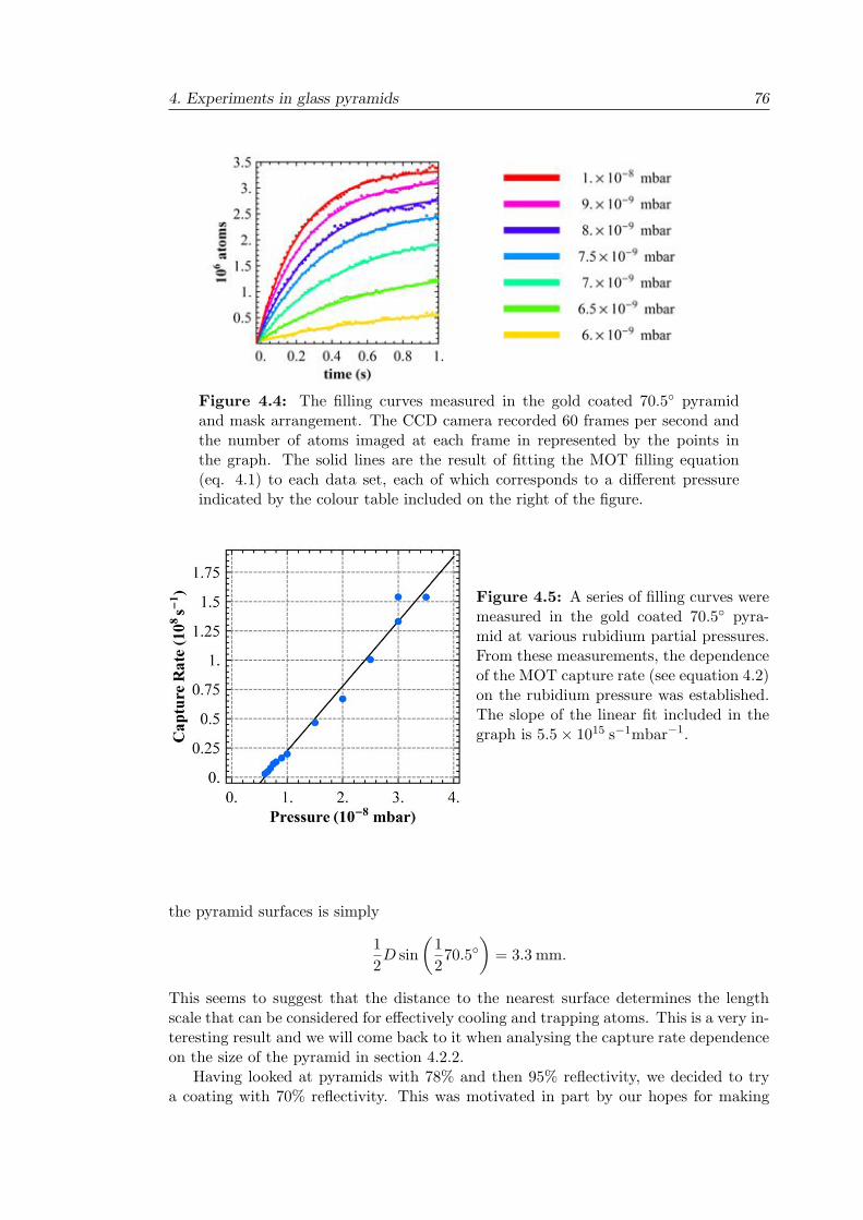
4. Experiments in glass pyramids 76
Figure 4.4: The filling curves measured in the gold coated 70.5! pyramidand mask arrangement. The CCD camera recorded 60 frames per second andthe number of atoms imaged at each frame in represented by the points inthe graph. The solid lines are the result of fitting the MOT filling equation(eq. 4.1) to each data set, each of which corresponds to a di"erent pressureindicated by the colour table included on the right of the figure.
Figure 4.5: A series of filling curves weremeasured in the gold coated 70.5! pyra-mid at various rubidium partial pressures.From these measurements, the dependenceof the MOT capture rate (see equation 4.2)on the rubidium pressure was established.The slope of the linear fit included in thegraph is 5.5# 1015 s"1mbar"1.
the pyramid surfaces is simply
12D sin
)1270.5!
*= 3.3 mm.
This seems to suggest that the distance to the nearest surface determines the lengthscale that can be considered for e"ectively cooling and trapping atoms. This is a very in-teresting result and we will come back to it when analysing the capture rate dependenceon the size of the pyramid in section 4.2.2.
Having looked at pyramids with 78% and then 95% reflectivity, we decided to trya coating with 70% reflectivity. This was motivated in part by our hopes for making
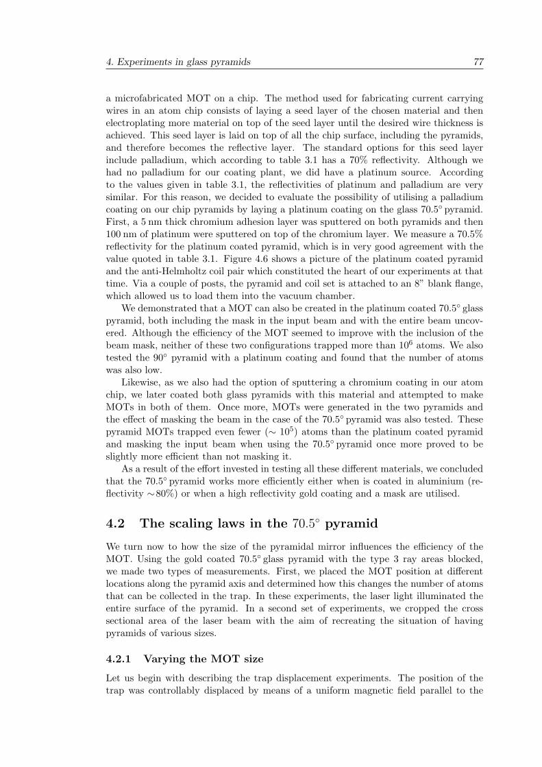
4. Experiments in glass pyramids 77
a microfabricated MOT on a chip. The method used for fabricating current carryingwires in an atom chip consists of laying a seed layer of the chosen material and thenelectroplating more material on top of the seed layer until the desired wire thickness isachieved. This seed layer is laid on top of all the chip surface, including the pyramids,and therefore becomes the reflective layer. The standard options for this seed layerinclude palladium, which according to table 3.1 has a 70% reflectivity. Although wehad no palladium for our coating plant, we did have a platinum source. Accordingto the values given in table 3.1, the reflectivities of platinum and palladium are verysimilar. For this reason, we decided to evaluate the possibility of utilising a palladiumcoating on our chip pyramids by laying a platinum coating on the glass 70.5! pyramid.First, a 5 nm thick chromium adhesion layer was sputtered on both pyramids and then100 nm of platinum were sputtered on top of the chromium layer. We measure a 70.5%reflectivity for the platinum coated pyramid, which is in very good agreement with thevalue quoted in table 3.1. Figure 4.6 shows a picture of the platinum coated pyramidand the anti-Helmholtz coil pair which constituted the heart of our experiments at thattime. Via a couple of posts, the pyramid and coil set is attached to an 8” blank flange,which allowed us to load them into the vacuum chamber.
We demonstrated that a MOT can also be created in the platinum coated 70.5! glasspyramid, both including the mask in the input beam and with the entire beam uncov-ered. Although the e!ciency of the MOT seemed to improve with the inclusion of thebeam mask, neither of these two configurations trapped more than 106 atoms. We alsotested the 90! pyramid with a platinum coating and found that the number of atomswas also low.
Likewise, as we also had the option of sputtering a chromium coating in our atomchip, we later coated both glass pyramids with this material and attempted to makeMOTs in both of them. Once more, MOTs were generated in the two pyramids andthe e"ect of masking the beam in the case of the 70.5! pyramid was also tested. Thesepyramid MOTs trapped even fewer (! 105) atoms than the platinum coated pyramidand masking the input beam when using the 70.5! pyramid once more proved to beslightly more e!cient than not masking it.
As a result of the e"ort invested in testing all these di"erent materials, we concludedthat the 70.5! pyramid works more e!ciently either when is coated in aluminium (re-flectivity !80%) or when a high reflectivity gold coating and a mask are utilised.
4.2 The scaling laws in the 70.50 pyramid
We turn now to how the size of the pyramidal mirror influences the e!ciency of theMOT. Using the gold coated 70.5! glass pyramid with the type 3 ray areas blocked,we made two types of measurements. First, we placed the MOT position at di"erentlocations along the pyramid axis and determined how this changes the number of atomsthat can be collected in the trap. In these experiments, the laser light illuminated theentire surface of the pyramid. In a second set of experiments, we cropped the crosssectional area of the laser beam with the aim of recreating the situation of havingpyramids of various sizes.
4.2.1 Varying the MOT size
Let us begin with describing the trap displacement experiments. The position of thetrap was controllably displaced by means of a uniform magnetic field parallel to the
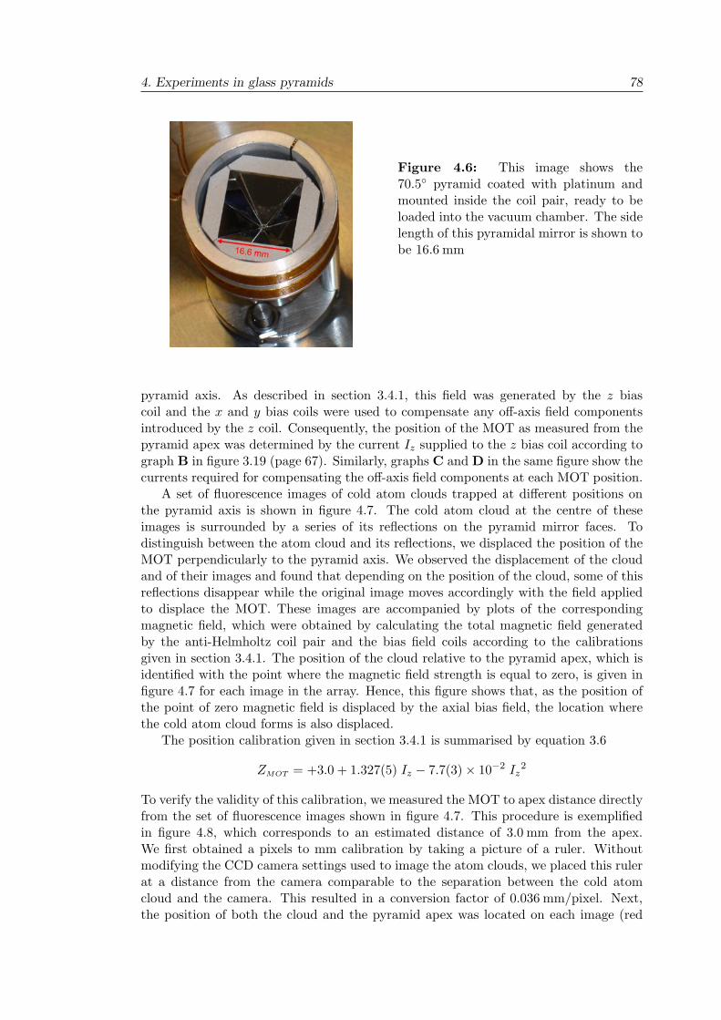
4. Experiments in glass pyramids 78
Figure 4.6: This image shows the70.5! pyramid coated with platinum andmounted inside the coil pair, ready to beloaded into the vacuum chamber. The sidelength of this pyramidal mirror is shown tobe 16.6 mm
pyramid axis. As described in section 3.4.1, this field was generated by the z biascoil and the x and y bias coils were used to compensate any o"-axis field componentsintroduced by the z coil. Consequently, the position of the MOT as measured from thepyramid apex was determined by the current Iz supplied to the z bias coil according tograph B in figure 3.19 (page 67). Similarly, graphs C and D in the same figure show thecurrents required for compensating the o"-axis field components at each MOT position.
A set of fluorescence images of cold atom clouds trapped at di"erent positions onthe pyramid axis is shown in figure 4.7. The cold atom cloud at the centre of theseimages is surrounded by a series of its reflections on the pyramid mirror faces. Todistinguish between the atom cloud and its reflections, we displaced the position of theMOT perpendicularly to the pyramid axis. We observed the displacement of the cloudand of their images and found that depending on the position of the cloud, some of thisreflections disappear while the original image moves accordingly with the field appliedto displace the MOT. These images are accompanied by plots of the correspondingmagnetic field, which were obtained by calculating the total magnetic field generatedby the anti-Helmholtz coil pair and the bias field coils according to the calibrationsgiven in section 3.4.1. The position of the cloud relative to the pyramid apex, which isidentified with the point where the magnetic field strength is equal to zero, is given infigure 4.7 for each image in the array. Hence, this figure shows that, as the position ofthe point of zero magnetic field is displaced by the axial bias field, the location wherethe cold atom cloud forms is also displaced.
The position calibration given in section 3.4.1 is summarised by equation 3.6
ZMOT = +3.0 + 1.327(5) Iz " 7.7(3)# 10"2 Iz2
To verify the validity of this calibration, we measured the MOT to apex distance directlyfrom the set of fluorescence images shown in figure 4.7. This procedure is exemplifiedin figure 4.8, which corresponds to an estimated distance of 3.0 mm from the apex.We first obtained a pixels to mm calibration by taking a picture of a ruler. Withoutmodifying the CCD camera settings used to image the atom clouds, we placed this rulerat a distance from the camera comparable to the separation between the cold atomcloud and the camera. This resulted in a conversion factor of 0.036 mm/pixel. Next,the position of both the cloud and the pyramid apex was located on each image (red
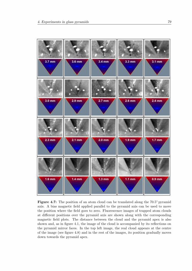
4. Experiments in glass pyramids 79
Figure 4.7: The position of an atom cloud can be translated along the 70.5! pyramidaxis. A bias magnetic field applied parallel to the pyramid axis can be used to movethe position where the field goes to zero. Fluorescence images of trapped atom cloudsat di"erent positions over the pyramid axis are shown along with the correspondingmagnetic field plots. The distance between the cloud and the pyramid apex is alsoshown and, as in figure 4.1, the image of the cloud is accompanied by its reflections onthe pyramid mirror faces. In the top left image, the real cloud appears at the centreof the image (see figure 4.8) and in the rest of the images, its position gradually movesdown towards the pyramid apex.
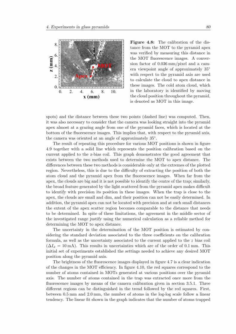
4. Experiments in glass pyramids 80
Figure 4.8: The calibration of the dis-tance from the MOT to the pyramid apexwas verified by measuring this distance inthe MOT fluorescence images. A conver-sion factor of 0.036 mm/pixel and a cam-era viewpoint angle of approximately 35!
with respect to the pyramid axis are usedto calculate the cloud to apex distance inthese images. The cold atom cloud, whichin the laboratory is identified by movingthe cloud position throughout the pyramid,is denoted as MOT in this image.
spots) and the distance between these two points (dashed line) was computed. Then,it was also necessary to consider that the camera was looking straight into the pyramidapex almost at a grazing angle from one of the pyramid faces, which is located at thebottom of the fluorescence images. This implies that, with respect to the pyramid axis,the camera was oriented at an angle of approximately 35!.
The result of repeating this procedure for various MOT positions is shown in figure4.9 together with a solid line which represents the position calibration based on thecurrent applied to the z-bias coil. This graph demonstrates the good agreement thatexists between the two methods used to determine the MOT to apex distance. Thedi"erences between these two methods is considerable only at the extremes of the plottedregion. Nevertheless, this is due to the di!culty of extracting the position of both theatom cloud and the pyramid apex from the fluorescence images. When far from theapex, the clouds are big and it is not possible to identify the centre of the trap; similarly,the broad feature generated by the light scattered from the pyramid apex makes di!cultto identify with precision its position in these images. When the trap is close to theapex, the clouds are small and dim, and their position can not be easily determined. Inaddition, the pyramid apex can not be located with precision and at such small distancesthe extent of the apex scatter region becomes comparable to the distance that needsto be determined. In spite of these limitations, the agreement in the middle sector ofthe investigated range justify using the numerical calculation as a reliable method fordetermining the MOT to apex distance.
The uncertainty in the determination of the MOT position is estimated by con-sidering the standard deviation associated to the three coe!cients on the calibrationformula, as well as the uncertainty associated to the current applied to the z bias coil($IZ = 10 mA). This results in uncertainties which are of the order of 0.1 mm. Thisinitial set of experiments established the settings needed to achieve any desired MOTposition along the pyramid axis.
The brightness of the fluorescence images displayed in figure 4.7 is a clear indicationof the changes in the MOT e!ciency. In figure 4.10, the red squares correspond to thenumber of atoms contained in MOTs generated at various positions over the pyramidaxis. The number of atoms contained in the trap was extracted once more from thefluorescence images by means of the camera calibration given in section 3.5.1. Threedi"erent regions can be distinguished in the trend followed by the red squares. First,between 0.5 mm and 2.0 mm, the number of atoms in the log-log scale follow a lineartendency. The linear fit shown in the graph indicates that the number of atoms trapped
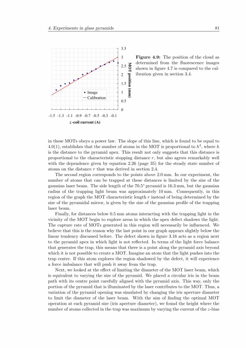
4. Experiments in glass pyramids 81
0
0.5
1
1.5
2
2.5
3
3.5
-1.5 -1.3 -1.1 -0.9 -0.7 -0.5 -0.3 -0.1
z -coil current (A)
MO
T p
ositio
n (m
m)
Image
Calibration
Figure 4.9: The position of the cloud asdetermined from the fluorescence imagesshown in figure 4.7 is compared to the cal-ibration given in section 3.4.
in these MOTs obeys a power law. The slope of this line, which is found to be equal to4.0(1), establishes that the number of atoms in the MOT is proportional to h4, where his the distance to the pyramid apex. This result not only suggests that this distance isproportional to the characteristic stopping distance r, but also agrees remarkably wellwith the dependence given by equation 2.26 (page 35) for the steady state number ofatoms on the distance r that was derived in section 2.4.
The second region corresponds to the points above 2.0 mm. In our experiment, thenumber of atoms that can be trapped at these distances is limited by the size of thegaussian laser beam. The side length of the 70.5! pyramid is 16.3 mm, but the gaussianradius of the trapping light beam was approximately 10 mm. Consequently, in thisregion of the graph the MOT characteristic length r instead of being determined by thesize of the pyramidal mirror, is given by the size of the gaussian profile of the trappinglaser beam.
Finally, for distances below 0.5 mm atoms interacting with the trapping light in thevicinity of the MOT begin to explore areas in which the apex defect shadows the light.The capture rate of MOTs generated in this region will necessarily be influenced. Webelieve that this is the reason why the last point in our graph appears slightly below thelinear tendency discussed before. The defect shown in figure 3.16 acts as a region nextto the pyramid apex in which light is not reflected. In terms of the light force balancethat generates the trap, this means that there is a point along the pyramid axis beyondwhich it is not possible to create a MOT. Imagine an atom that the light pushes into thetrap centre. If this atom explores the region shadowed by the defect, it will experiencea force imbalance that will push it away from the trap.
Next, we looked at the e"ect of limiting the diameter of the MOT laser beam, whichis equivalent to varying the size of the pyramid. We placed a circular iris in the beampath with its centre point carefully aligned with the pyramid axis. This way, only theportion of the pyramid that is illuminated by the laser contributes to the MOT. Thus, avariation of the pyramid opening was simulated by changing the iris aperture diameterto limit the diameter of the laser beam. With the aim of finding the optimal MOToperation at each pyramid size (iris aperture diameter), we found the height where thenumber of atoms collected in the trap was maximum by varying the current of the z-bias
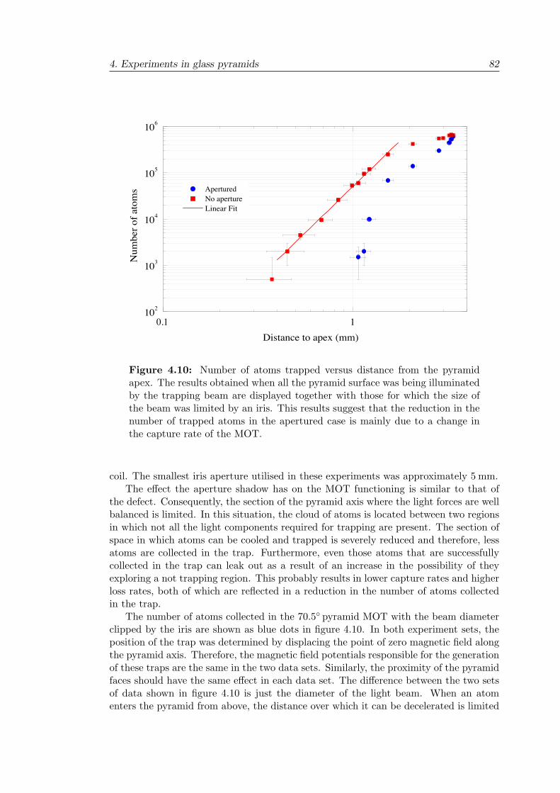
4. Experiments in glass pyramids 82
0.1 1102
103
104
105
106
Num
ber o
f ato
ms
Distance to apex (mm)
Apertured No aperture Linear Fit
Figure 4.10: Number of atoms trapped versus distance from the pyramidapex. The results obtained when all the pyramid surface was being illuminatedby the trapping beam are displayed together with those for which the size ofthe beam was limited by an iris. This results suggest that the reduction in thenumber of trapped atoms in the apertured case is mainly due to a change inthe capture rate of the MOT.
coil. The smallest iris aperture utilised in these experiments was approximately 5 mm.The e"ect the aperture shadow has on the MOT functioning is similar to that of
the defect. Consequently, the section of the pyramid axis where the light forces are wellbalanced is limited. In this situation, the cloud of atoms is located between two regionsin which not all the light components required for trapping are present. The section ofspace in which atoms can be cooled and trapped is severely reduced and therefore, lessatoms are collected in the trap. Furthermore, even those atoms that are successfullycollected in the trap can leak out as a result of an increase in the possibility of theyexploring a not trapping region. This probably results in lower capture rates and higherloss rates, both of which are reflected in a reduction in the number of atoms collectedin the trap.
The number of atoms collected in the 70.5! pyramid MOT with the beam diameterclipped by the iris are shown as blue dots in figure 4.10. In both experiment sets, theposition of the trap was determined by displacing the point of zero magnetic field alongthe pyramid axis. Therefore, the magnetic field potentials responsible for the generationof these traps are the same in the two data sets. Similarly, the proximity of the pyramidfaces should have the same e"ect in each data set. The di"erence between the two setsof data shown in figure 4.10 is just the diameter of the light beam. When an atomenters the pyramid from above, the distance over which it can be decelerated is limited
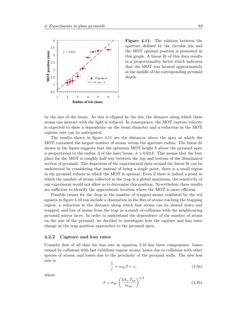
4. Experiments in glass pyramids 83
y = 0.62x
0.5
1
1.5
2
2.5
3
3.5
4
1 2 3 4 5 6 7
Radius of iris (mm)
MO
T p
osi
tio
n (
mm
)
Figure 4.11: The relation between theaperture defined by the circular iris andthe MOT optimal position is presented inthis graph. A linear fit of this data resultsin a proportionality factor which indicatesthat the MOT was located approximatelyat the middle of the corresponding pyramiddepth.
by the size of the beam. As this is clipped by the iris, the distance along which theseatoms can interact with the light is reduced. In consequence, the MOT capture velocityis expected to show a dependence on the beam diameter and a reduction in the MOTcapture rate can be anticipated.
The results shown in figure 4.11 are the distances above the apex at which theMOT contained the largest number of atoms versus the aperture radius. The linear fitshown in the figure suggests that the optimum MOT height h above the pyramid apexis proportional to the radius A of the laser beam: h + 0.62A. This means that the bestplace for the MOT is roughly half way between the top and bottom of the illuminatedsection of pyramid. The dispersion of the experimental data around the linear fit can beunderstood by considering that instead of being a single point, there is a small regionin the pyramid volume in which the MOT is optimal. Even if there is indeed a point inwhich the number of atoms collected in the trap is a global maximum, the sensitivity ofour experiment would not allow us to determine this position. Nevertheless, these resultsare su!cient to identify the approximate location where the MOT is more e!cient.
Possible causes for the drop in the number of trapped atoms exhibited by the redsquares in figure 4.10 can include a diminution in the flux of atoms reaching the trappingregion; a reduction in the distance along which fast atoms can be slowed down andtrapped; and loss of atoms from the trap as a result of collisions with the neighbouringpyramid mirror faces. In order to understand the dependence of the number of atomson the size of the pyramid, we decided to investigate how the capture and loss rateschange as the trap position approaches to the pyramid apex.
4.2.2 Capture and loss rates
Consider first of all that the loss rate in equation 2.16 has three components: lossescaused by collisions with fast rubidium vapour atoms; losses due to collisions with otherspecies of atoms; and losses due to the proximity of the pyramid walls. The new lossrate is
1"
= nRb# + (, (4.3a)
where
# = ,Rb
)3 kB TRb
mRb
*1/2
(4.3b)
4. Experiments in glass pyramids 84
and
( = nb ,b
)3 kB Tb
mb
*1/2
+1"w
. (4.3c)
Similarly, the capture rate given in equation 2.16, can be explicitly expressed in termsof the rubidium atom density
R = $nRb (4.3d)
With these definitions the MOT filling rate equation is
dN
dt= $nRb " [#nRb + (]N (4.4)
which, with the initial condition N(0) = 0, has the solution
N(t) = Ns
%1" e"('nRb+%)t
&(4.5)
where, the steady state number of atoms is
Ns =$nRb
#nRb + ((4.6)
We have measured the capture and loss rates from MOT loading curves (figures 4.12and 4.13) taken at di"erent positions along the pyramid axis and at various rubidiumpressures. As before, the position of the cloud was controlled by the application ofappropriate bias fields. The rubidium pressure was controlled by varying the currentsupplied to the rubidium dispenser and its value was determined with the calibrationgiven in section 3.1.2
PRb (I) = 4# 10"16e2.97(9) I (4.7)
where the current is given in Amperes and the pressure in mbar. The loading curveswere obtained by first switching on the anti-Helmholtz coils and then capturing series offluorescence images as a cold atom cloud was collected in the trap. Firstly, a backgroundlight image was taken immediately before feeding current to the coils. Then, the firstimage of the filling curve was taken immediately after the coils current was switchedon and then a new image was captured every 50 ms, until a total of 20 images (950 ms)had been taken. This sequence of images was taken several times for each pair of MOTposition and pressure values.
The number of atoms as a function of time was extracted from each sequence ofimages. First, the background image was subtracted from each image in the fillingsequence. In addition, to minimise the noise introduced by variations of the backgroundlight between the filling curve images and the background image, a region of interestcontaining exclusively the section of the image where the MOT is visible was selected.To determine the number of atoms in each frame of the filling, all the pixel values in thesubtracted image were summed and the resulting value was substituted in the cameracalibration formula deduced in section 3.5.1.
Figures 4.12 and 4.13 contain the MOT filling data sets that we measured. Eachcolour in these graphs corresponds to a single MOT filling sequence. The solid curvesare the result of a least-squares fitting of equation 4.5 to each filling sequence, with thesteady state number of atoms Ns and the 1/e life-time " as the fitting parameters. Foreach MOT filling sequence, the standard deviation associated to the estimate of Ns istypically a 4% of the estimated value. Similarly, a typical standard deviation of 10% is
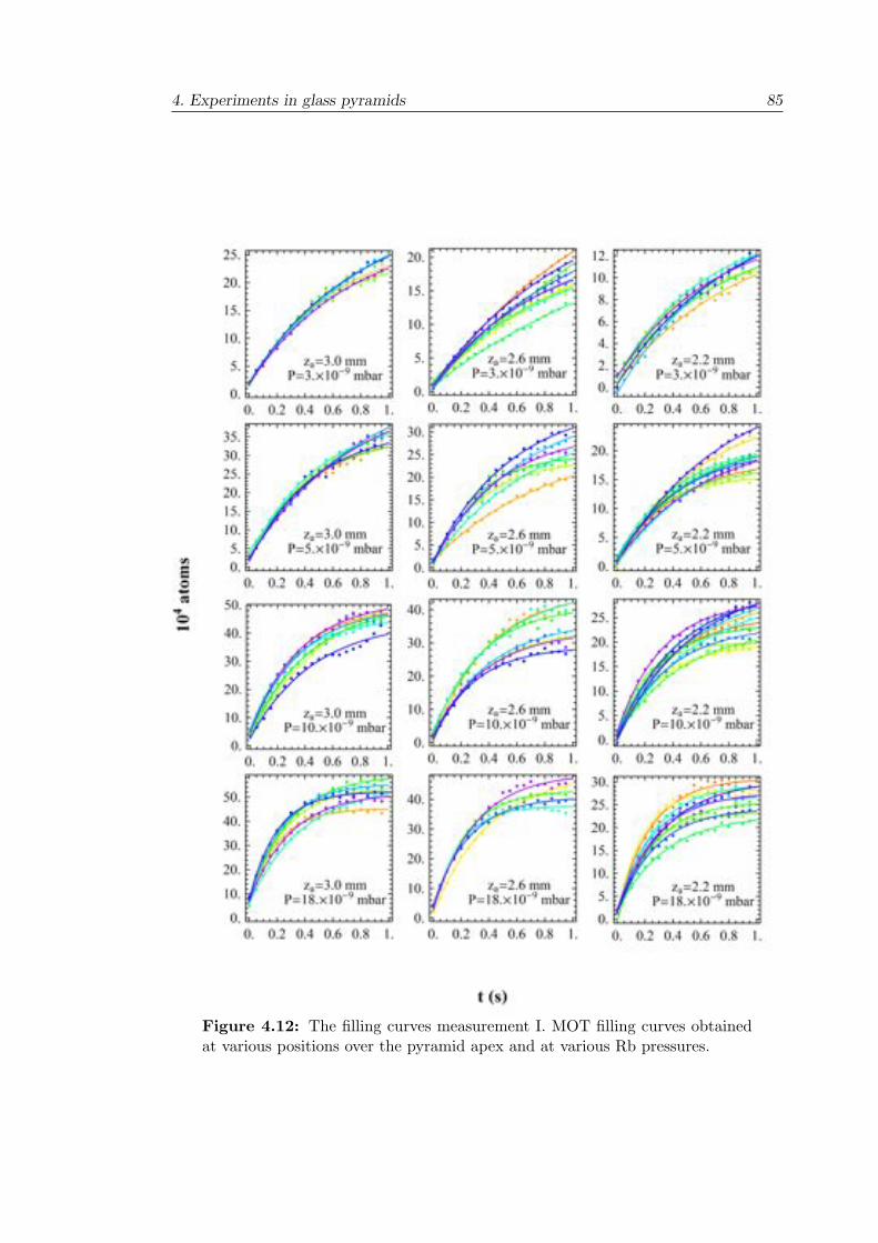
4. Experiments in glass pyramids 85
Figure 4.12: The filling curves measurement I. MOT filling curves obtainedat various positions over the pyramid apex and at various Rb pressures.
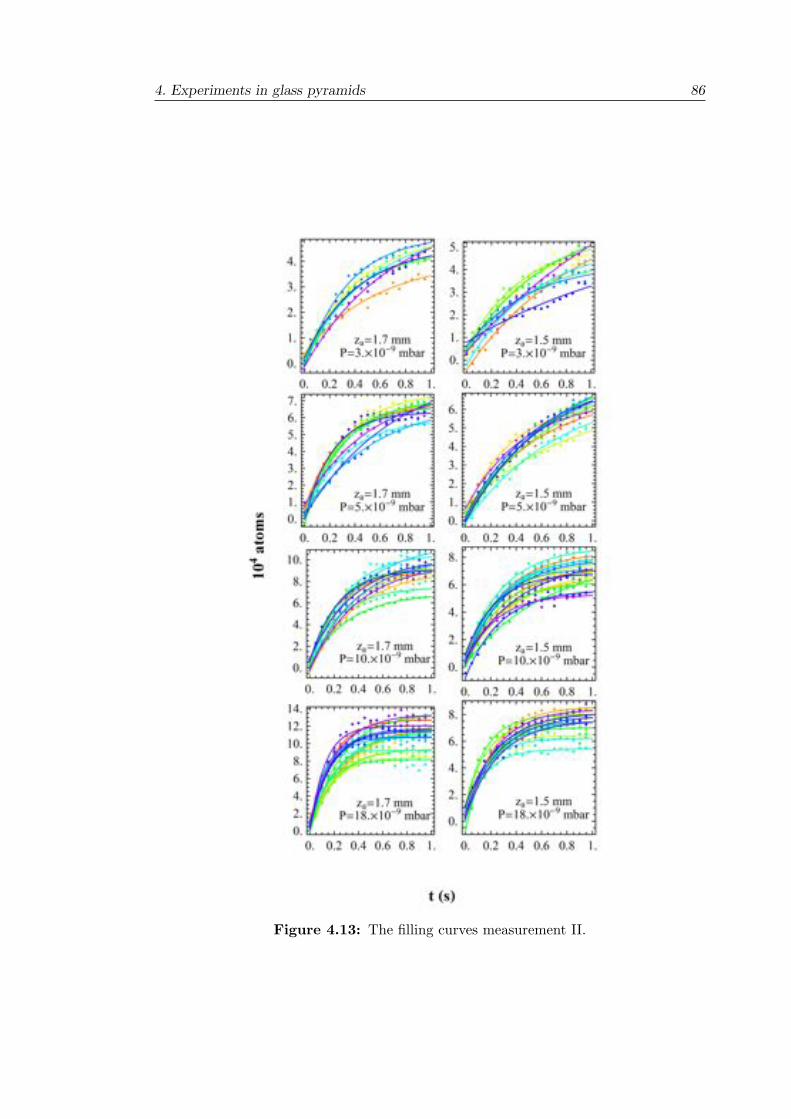
4. Experiments in glass pyramids 86
Figure 4.13: The filling curves measurement II.
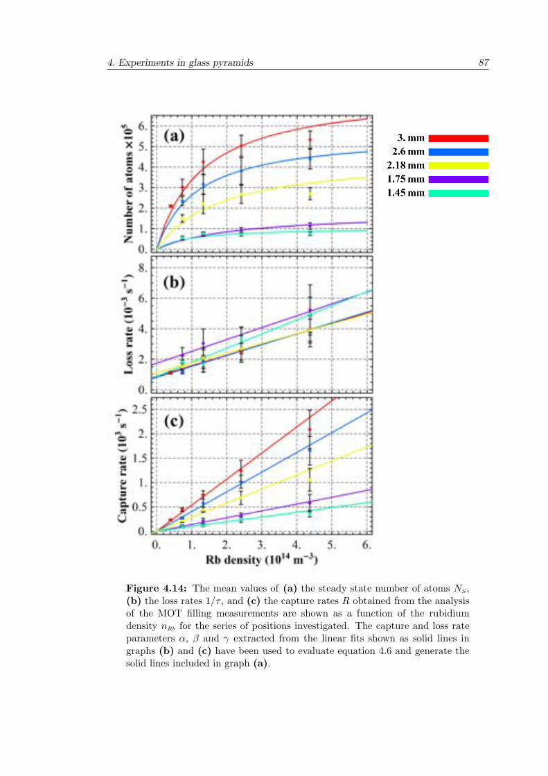
4. Experiments in glass pyramids 87
Figure 4.14: The mean values of (a) the steady state number of atoms NS,(b) the loss rates 1/" , and (c) the capture rates R obtained from the analysisof the MOT filling measurements are shown as a function of the rubidiumdensity nRb for the series of positions investigated. The capture and loss rateparameters $, # and ( extracted from the linear fits shown as solid lines ingraphs (b) and (c) have been used to evaluate equation 4.6 and generate thesolid lines included in graph (a).
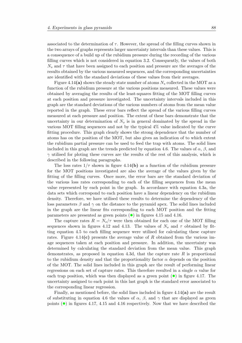
4. Experiments in glass pyramids 88
associated to the determination of " . However, the spread of the filling curves shown inthe two arrays of graphs represents larger uncertainty intervals than these values. This isa consequence of a build up of the rubidium pressure during the recording of the variousfilling curves which is not considered in equation 3.2. Consequently, the values of bothNs and " that have been assigned to each position and pressure are the averages of theresults obtained by the various measured sequences, and the corresponding uncertaintiesare identified with the standard deviations of these values from their averages.
Figure 4.14(a) shows the steady state number of atoms Ns collected in the MOT as afunction of the rubidium pressure at the various positions measured. These values wereobtained by averaging the results of the least-squares fitting of the MOT filling curvesat each position and pressure investigated. The uncertainty intervals included in thisgraph are the standard deviations of the various numbers of atoms from the mean valuereported in the graph. These error bars reflect the spread of the various filling curvesmeasured at each pressure and position. The extent of these bars demonstrate that theuncertainty in our determination of Ns is in general dominated by the spread in thevarious MOT filling sequences and not by the typical 4% value indicated by the curvefitting procedure. This graph clearly shows the strong dependence that the number ofatoms has on the position of the MOT, but also gives an indication of to which extentthe rubidium partial pressure can be used to feed the trap with atoms. The solid linesincluded in this graph are the trends predicted by equation 4.6. The values of $, #, and( utilised for ploting these curves are the results of the rest of this analysis, which isdescribed in the following paragraphs.
The loss rates 1/" shown in figure 4.14(b) as a function of the rubidium pressurefor the MOT positions investigated are also the average of the values given by thefitting of the filling curves. Once more, the error bars are the standard deviation ofthe various loss rates corresponding to each of the filling sequences from the meanvalue represented by each point in the graph. In accordance with equation 4.3a, thedata sets which correspond to each position have a linear dependency on the rubidiumdensity. Therefore, we have utilised these results to determine the dependency of theloss parameters # and ( on the distance to the pyramid apex. The solid lines includedin the graph are the linear fits corresponding to each MOT position and the fittingparameters are presented as green points (•) in figures 4.15 and 4.16.
The capture rates R = Ns/" were then obtained for each one of the MOT fillingsequences shown in figures 4.12 and 4.13. The values of Ns and " obtained by fit-ting equation 4.5 to each filling sequence were utilised for calculating these capturerates. Figure 4.14(c) presents the average value of R obtained from the various im-age sequences taken at each position and pressure. In addition, the uncertainty wasdetermined by calculating the standard deviation from the mean value. This graphdemonstrates, as proposed in equation 4.3d, that the capture rate R is proportionalto the rubidium density and that the proportionality factor $ depends on the positionof the MOT. The solid lines included in this graph are the result of performing linearregressions on each set of capture rates. This therefore resulted in a single $ value foreach trap position, which was then displayed as a green point (•) in figure 4.17. Theuncertainty assigned to each point in this last graph is the standard error associated tothe corresponding linear regression.
Finally, as mentioned before, the solid lines included in figure 4.14(a) are the resultof substituting in equation 4.6 the values of $, #, and ( that are displayed as greenpoints (•) in figures 4.17, 4.15 and 4.16 respectively. Now that we have described the
4. Experiments in glass pyramids 89
Figure 4.15: The proportionality factor # relating the loss rate and the ru-bidium vapour density for each of the MOT positions investigated.
methodology followed for obtaining the data contained in these three graphs, in thefollowing paragraphs we will discuss these results.
The factor of proportionality between the MOT loss rate and the rubidium density #is displayed as a function of the distance from the apex in figure 4.15. These points andtheir error bars, as we have already mentioned, are the slopes obtained from the linearregressions shown in graph 4.14(b) and their corresponding standard errors respectively.At the beginning of this section we presented a model in which the dependence of theMOT loss rate on the pyramid walls is absorbed on the term led by the parameter (.However, the growth on the value of # as the MOT approaches to the pyramid apexsuggests that there is a dependence of the rubidium atom density on the distance tothe pyramid surfaces. Rubidium atoms in the vapour are continuously being absorbedand desorbed from these surfaces and this could have lead to an enhancement of theloss rate caused by collisions with the desorbed atoms.
The results shown in figure 4.15 can be used to estimate the cross section for collisionsbetween background vapour rubidium atoms and trapped atoms. To keep this simple,we have calculated a single # value by averaging the data points shown in figure 4.15,which results in a value of (7.9 ± 1.4)# 10"15 m3s"1. We then obtained the Rb-Rbcollision cross section by dividing this average value of # by the mean velocity v of thenon-trapped, room temperature rubidium atoms, which we assumed to be at a pressureof 10"9 mbar. In addition, for simplicity we restricted ourselves to considering collisionsbetween 85Rb atoms. This way, the average of # results in a collision cross section of2.7(5)# 10"13 cm2. This value is in good agreement with the value of 3# 10"13 cm2
reported by Rapol et al. [85].Note that in the range of distances investigated, the parameter that determines the
loss rate dependence on the distance from the pyramid apex (, which is given in figure4.16 also as green points (•), does not show a significant change. As a result of thelimitations imposed by the quality of the pyramid replica, the shortest distance to theapex achieved in our experiments was approximately 1 mm. Let z = h be the positionwhere the cloud sits as measured from the pyramid apex. Then, the perpendicular
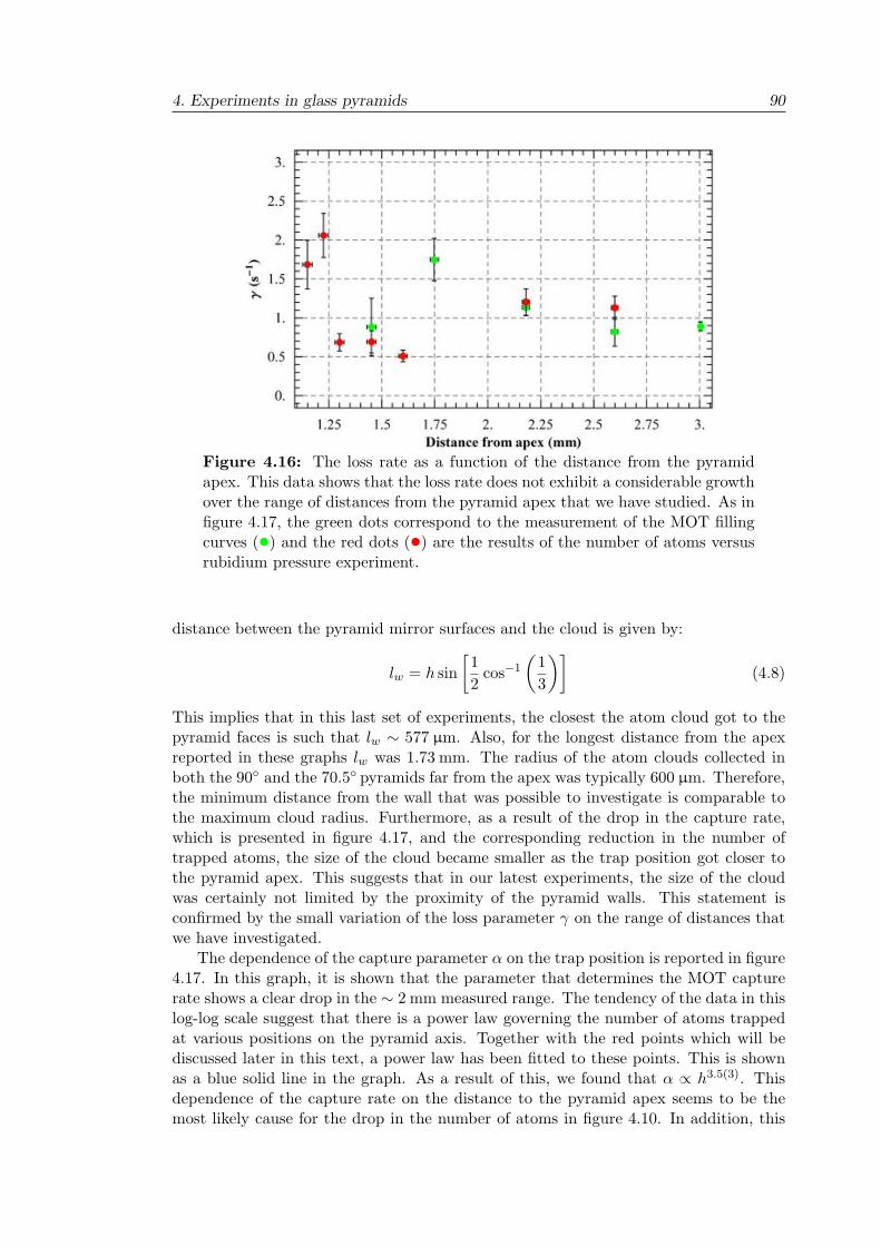
4. Experiments in glass pyramids 90
Figure 4.16: The loss rate as a function of the distance from the pyramidapex. This data shows that the loss rate does not exhibit a considerable growthover the range of distances from the pyramid apex that we have studied. As infigure 4.17, the green dots correspond to the measurement of the MOT fillingcurves (•) and the red dots (•) are the results of the number of atoms versusrubidium pressure experiment.
distance between the pyramid mirror surfaces and the cloud is given by:
lw = h sin-12
cos"1
)13
*.(4.8)
This implies that in this last set of experiments, the closest the atom cloud got to thepyramid faces is such that lw ! 577 µm. Also, for the longest distance from the apexreported in these graphs lw was 1.73 mm. The radius of the atom clouds collected inboth the 90! and the 70.5! pyramids far from the apex was typically 600 µm. Therefore,the minimum distance from the wall that was possible to investigate is comparable tothe maximum cloud radius. Furthermore, as a result of the drop in the capture rate,which is presented in figure 4.17, and the corresponding reduction in the number oftrapped atoms, the size of the cloud became smaller as the trap position got closer tothe pyramid apex. This suggests that in our latest experiments, the size of the cloudwas certainly not limited by the proximity of the pyramid walls. This statement isconfirmed by the small variation of the loss parameter ( on the range of distances thatwe have investigated.
The dependence of the capture parameter $ on the trap position is reported in figure4.17. In this graph, it is shown that the parameter that determines the MOT capturerate shows a clear drop in the ! 2 mm measured range. The tendency of the data in thislog-log scale suggest that there is a power law governing the number of atoms trappedat various positions on the pyramid axis. Together with the red points which will bediscussed later in this text, a power law has been fitted to these points. This is shownas a blue solid line in the graph. As a result of this, we found that $ / h3.5(3). Thisdependence of the capture rate on the distance to the pyramid apex seems to be themost likely cause for the drop in the number of atoms in figure 4.10. In addition, this
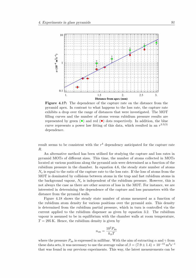
4. Experiments in glass pyramids 91
Figure 4.17: The dependence of the capture rate on the distance from thepyramid apex. In contrast to what happens to the loss rate, the capture rateexhibits a drop over the range of distances that were investigated. The MOTfilling curves and the number of atoms versus rubidium pressure results arerepresented by green (•) and red (•) dots respectively. In addition, the bluecurve represents a power law fitting of this data, which resulted in an r3.5(3)
dependence.
result seems to be consistent with the r4 dependency anticipated for the capture rateR.
An alternative method has been utilised for studying the capture and loss rates inpyramid MOTs of di"erent sizes. This time, the number of atoms collected in MOTslocated at various positions along the pyramid axis were determined as a function of therubidium pressure in the chamber. In equation 4.6, the steady state number of atomsNs is equal to the ratio of the capture rate to the loss rate. If the loss of atoms from theMOT is dominated by collisions between atoms in the trap and fast rubidium atoms inthe background vapour, Ns is independent of the rubidium pressure. However, this isnot always the case as there are other sources of loss in the MOT. For instance, we areinterested in determining the dependence of the capture and loss parameters with thedistance from the pyramid walls.
Figure 4.18 shows the steady state number of atoms measured as a function ofthe rubidium atom density for various positions over the pyramid axis. This densityis determined from the rubidium partial pressure, which in turn is controlled via thecurrent applied to the rubidium dispenser as given by equation 3.2. The rubidiumvapour is assumed to be in equilibrium with the chamber walls at room temperature,T = 295 K. Hence, the rubidium density is given by
nRb =102PRb
kBT
where the pressure PRb is expressed in millibar. With the aim of extracting $ and ( fromthese data sets, it was necessary to use the average value of # = (7.9 ± 1.4)# 10"15 m3s"1
that was found in our previous experiments. This way, the latest measurements can be
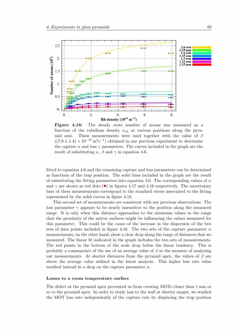
4. Experiments in glass pyramids 92
Figure 4.18: The steady state number of atoms was measured as afunction of the rubidium density nRb at various positions along the pyra-mid axis. These measurements were used together with the value of #((7.9 ± 1.4)# 10"15 m3s"1) obtained in our previous experiment to determinethe capture $ and loss ( parameters. The curves included in the graph are theresult of substituting $, # and ( in equation 4.6.
fitted to equation 4.6 and the remaining capture and loss parameters can be determinedas functions of the trap position. The solid lines included in the graph are the resultof substituting the fitting parameters into equation 4.6. The corresponding values of $and ( are shown as red dots (•) in figures 4.17 and 4.16 respectively. The uncertaintybars of these measurements correspond to the standard errors associated to the fittingrepresented by the solid curves in figure 4.18.
This second set of measurements are consistent with our previous observations. Theloss parameter ( appears to be nearly insensitive to the position along the measuredrange. It is only when this distance approaches to the minimum values in the rangethat the proximity of the mirror surfaces might be influencing the values measured forthis parameter. This could be the cause of the increase in the dispersion of the twosets of data points included in figure 4.16. The two sets of the capture parameter $measurements, on the other hand, show a clear drop along the range of distances that wemeasured. The linear fit indicated in the graph includes the two sets of measurements.The red points in the bottom of the scale drop below the linear tendency. This isprobably a consequence of the use of an average value of # at the moment of analysingour measurements. At shorter distances from the pyramid apex, the values of # areabove the average value utilised in the latest analysis. This higher loss rate valueresulted instead in a drop on the capture parameter $.
Losses to a room temperature surface
The defect at the pyramid apex prevented us from creating MOTs closer than 1 mm orso to the pyramid apex. In order to study loss to the wall at shorter ranges, we studiedthe MOT loss rate independently of the capture rate by displacing the trap position
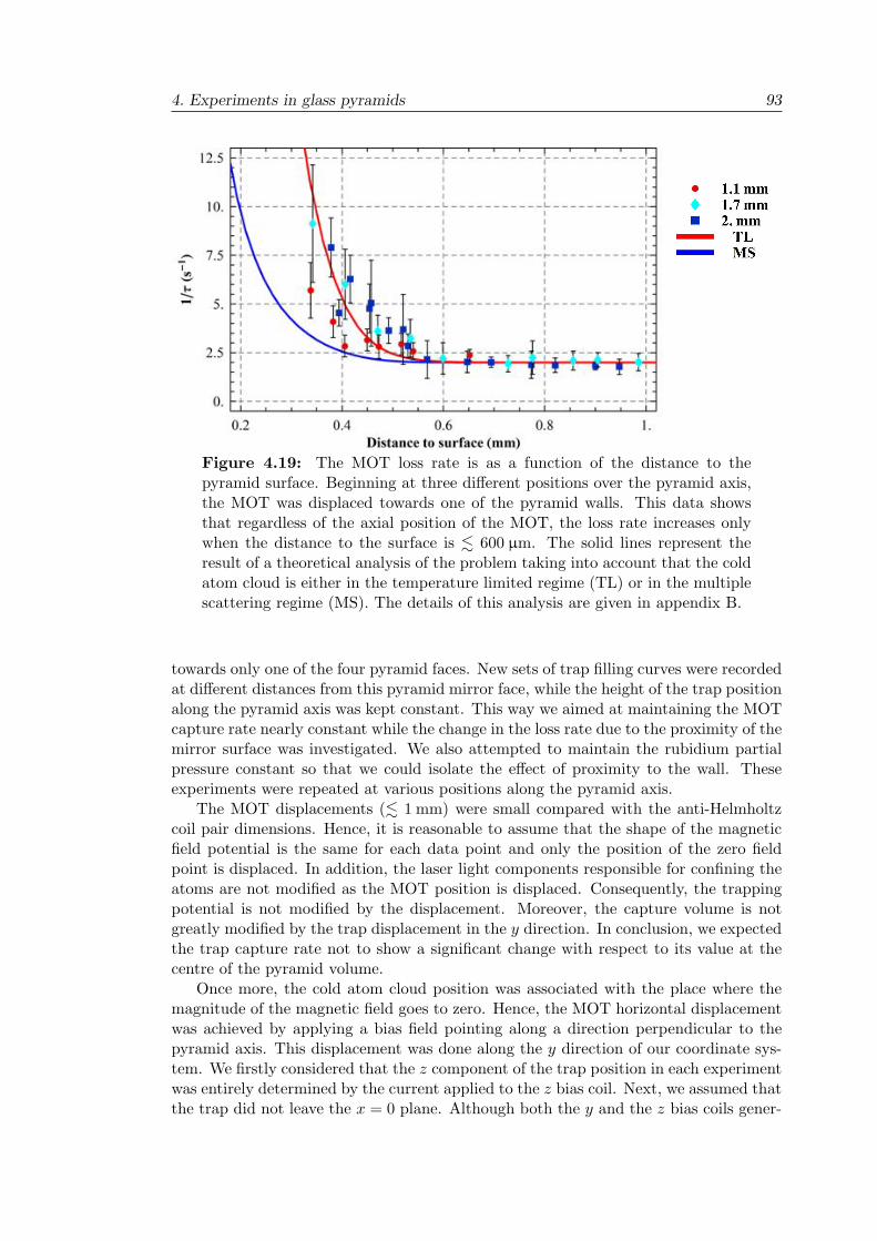
4. Experiments in glass pyramids 93
Figure 4.19: The MOT loss rate is as a function of the distance to thepyramid surface. Beginning at three di"erent positions over the pyramid axis,the MOT was displaced towards one of the pyramid walls. This data showsthat regardless of the axial position of the MOT, the loss rate increases onlywhen the distance to the surface is ! 600 µm. The solid lines represent theresult of a theoretical analysis of the problem taking into account that the coldatom cloud is either in the temperature limited regime (TL) or in the multiplescattering regime (MS). The details of this analysis are given in appendix B.
towards only one of the four pyramid faces. New sets of trap filling curves were recordedat di"erent distances from this pyramid mirror face, while the height of the trap positionalong the pyramid axis was kept constant. This way we aimed at maintaining the MOTcapture rate nearly constant while the change in the loss rate due to the proximity of themirror surface was investigated. We also attempted to maintain the rubidium partialpressure constant so that we could isolate the e"ect of proximity to the wall. Theseexperiments were repeated at various positions along the pyramid axis.
The MOT displacements (! 1 mm) were small compared with the anti-Helmholtzcoil pair dimensions. Hence, it is reasonable to assume that the shape of the magneticfield potential is the same for each data point and only the position of the zero fieldpoint is displaced. In addition, the laser light components responsible for confining theatoms are not modified as the MOT position is displaced. Consequently, the trappingpotential is not modified by the displacement. Moreover, the capture volume is notgreatly modified by the trap displacement in the y direction. In conclusion, we expectedthe trap capture rate not to show a significant change with respect to its value at thecentre of the pyramid volume.
Once more, the cold atom cloud position was associated with the place where themagnitude of the magnetic field goes to zero. Hence, the MOT horizontal displacementwas achieved by applying a bias field pointing along a direction perpendicular to thepyramid axis. This displacement was done along the y direction of our coordinate sys-tem. We firstly considered that the z component of the trap position in each experimentwas entirely determined by the current applied to the z bias coil. Next, we assumed thatthe trap did not leave the x = 0 plane. Although both the y and the z bias coils gener-
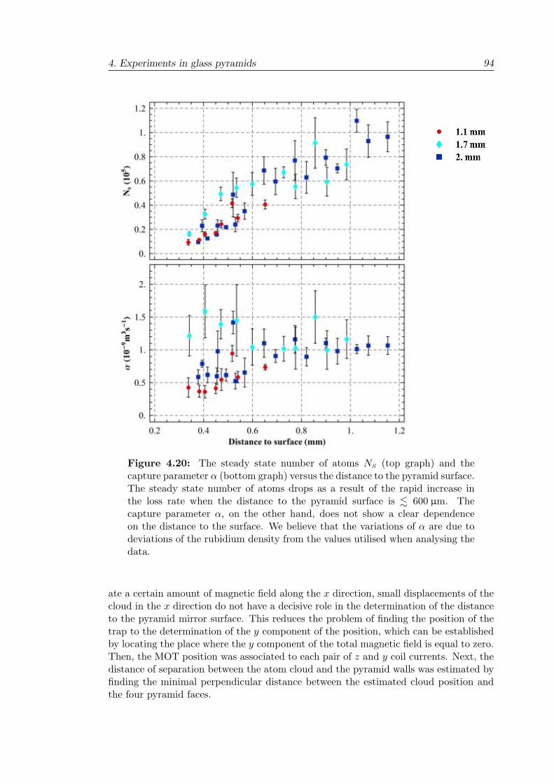
4. Experiments in glass pyramids 94
Figure 4.20: The steady state number of atoms NS (top graph) and thecapture parameter $ (bottom graph) versus the distance to the pyramid surface.The steady state number of atoms drops as a result of the rapid increase inthe loss rate when the distance to the pyramid surface is ! 600 µm. Thecapture parameter $, on the other hand, does not show a clear dependenceon the distance to the surface. We believe that the variations of $ are due todeviations of the rubidium density from the values utilised when analysing thedata.
ate a certain amount of magnetic field along the x direction, small displacements of thecloud in the x direction do not have a decisive role in the determination of the distanceto the pyramid mirror surface. This reduces the problem of finding the position of thetrap to the determination of the y component of the position, which can be establishedby locating the place where the y component of the total magnetic field is equal to zero.Then, the MOT position was associated to each pair of z and y coil currents. Next, thedistance of separation between the atom cloud and the pyramid walls was estimated byfinding the minimal perpendicular distance between the estimated cloud position andthe four pyramid faces.
4. Experiments in glass pyramids 95
The results of this last set of experiments are shown in figures 4.19 and 4.20. Theprocedure for recording the filling curves was the same as the one explained in section4.2.2. The first thing to note in figure 4.19 is that the contribution to the MOT lossrate that results from the interaction between trapped atoms and a neighbouring surfacebecomes important when the distance of separation between the centre of the cloud andthe surface becomes ! 600 µm. This threshold was already anticipated when discussingthe results obtained by displacing the MOT towards the pyramid apex and the newresults are in good agreement with our previous observations.
The loss rate value at which the experimental data approaches when the MOTwas located away from the mirror surface is also consistent with the results obtainedbefore. The average of the results shown in figure 4.15 resulted in a value of # of(7.9 ± 1.4)# 10"15 m3s"1. The current supplied to the Rb dispenser during the realisa-tion of these experiments was kept constant at 5.5 A, which corresponds to a sustainedRb pressure of 5.4# 10"9 mbar and to a Rb density of 1.3# 105 cm"3. This implies thatthe loss of atoms from the trap caused by collisions with background Rb atoms is char-acterised by a rate of #nRb * 1.04 s"1. Similarly, in figure 4.16 the loss rate componentthat is independent of the Rb vapour density ( when the cloud is far from the pyramidfaces is also of the order of 1 s"1. These two rates add to a value of (#nRb +(B) ! 2 s"1,which can also be seen in figure 4.19 as the value at which the total loss rate levels o"for the highest values of the distance from the surface.
The two solid curves included in figure 4.16 are the result of a theoretical estimationof the loss rate caused by the interaction of the trapped atoms and the surface of thepyramid. The details of the theoretical treatment of this problem are given in appendixB. Two di"erent regimes of MOT operation have been studied, the temperature limitedregime (TL) and the multiple scattering regime (MS). While in the temperature limitedregime, as more atoms are added to the trap, the cloud radius remains constant andthe density is determined by the total number of trapped atoms; in the multiple scat-tering regime, the density remains constant as the cloud grows and the cloud radius isdetermined by the total number of trapped atoms [103]. The red solid line included infigure 4.19 corresponds to the tendency predicted for the temperature limited regime(equation B.4).
(TL =ve"
12( d
! )2
%8&,
41 + Erf( d%
2()5 (4.9)
where Erf(x) denotes the Gauss error function
Erf(x) =2%&
+ x
0e"t2dt
In the range of positions investigated, our measurements (bottom graph in figure 4.20)indicate that the capture parameter $ takes a typical value of 10"9 m3s"1. This, to-gether with the Rb density at which these experiments were performed, results in acapture rate of 1.3# 105 s"1. In addition, we measured the 1/e radius of atom cloudswith small numbers of atoms both along its shortest and its longest directions, resultingin 80 µm and 120 µm respectively. Finally, (#nRb + (B) was taken to be 2 s"1. Theblue solid line is the result of considering a MOT in the multiple scattering regime (seeequation B.7). The capture rate used to generate this curve was the same as the one inthe temperature limited case. The trap density in this case should be independent of thetotal number of atoms contained in the cloud; its value was estimated by considering an
4. Experiments in glass pyramids 96
elliptical cloud containing 3# 104 atoms and extending over the same space consideredin the temperature limited case.
The di"erences on the trends followed by each set of loss rates is a result of adependence of the loss to the wall on the capture rate R. We have already shown thatthe capture rate is a function of the trap position along the pyramid axis. Each ofthe data sets shown in figure 4.19 was taken with a di"erent value of current runningthrough the z bias coil. Therefore the component of the trap to apex distance thatpoints along the pyramid axis direction was di"erent in each case. This distance hasbeen given for each data set at the top right corner of the figure. Similarly, althoughcare was taken in ensuring that the Rb partial pressure in the chamber, and thereforethe capture rate R, was maintained constant during the recording of the filling curves,there was a small variation between the recording of the di"erent data sets.
The values of the capture parameter $ which correspond to each data set in figure4.19 are shown in the bottom graph in figure 4.20. It is possible to appreciate thatfor each set of points, $ remains relatively constant as the trap position approachedthe mirror surface. We attribute the variations of this parameter to deviations of theRb density from the value of nRb = 1.3# 108 cm"3 used for analysing the data. Evenfor each z bias coil current, a build up of the Rb pressure in the chamber during therecording of the filling curves could have been responsible for a variation of the capturerate and consequently of the resulting trend followed by each set of loss rates.
The steady state number of atoms NS as a function of the distance to the mirrorsurface is shown in the top graph in figure 4.20. This graph reflects the variation of theloss rate. In the range between 600 µm and 1 mm, where the loss rate is nearly constant,the number of atoms also appears to be insensitive to the distance to the mirror. Onthe other hand, at distances below 600 µm the number of atoms collected in these trapsdrops as the position of the MOT approaches to the mirror surface. This is clearly aconsequence of the steep increase in the loss rate value as the capture rate does notshow any appreciable change in this same range of distances.
4.3 Summary
We have demonstrated that the geometry of the pyramidal mirrors fabricated in siliconwafers is suitable for cooling and trapping atoms. For this purpose, we fabricated a glassreplica of the silicon pyramid. A detailed numerical and experimental investigation ofthe optical properties of these pyramids led us to conclude that light firstly reflected inthe vicinity of these pyramid edges induces an imbalance in the MOT forces. Both theorientation and the polarisation state of this light when it crosses through the trappingregion are responsible for this imbalance. We also found that this undesired e"ectcan be either significantly reduced by depositing a limited reflectivity coating on the70.5! pyramids, or completely eliminated by patterning the reflective coating with theaim of suppressing these reflections. We tested a series of di"erent reflectivity coatingsand concluded that a ! 78% reflectivity gives the best results, generating a trap with 107
atoms, while a highly reflective (95%) gold coating prevented the MOT from functioning.To make a MOT in a 70.5! pyramid with such high reflectivity, we avoided depositingthe reflective layer in the area sections which produce these imbalancing reflections.This procedure was also succesful and resulted in MOTs that collected up to 107 atoms.
To estimate the number of atoms that can be trapped in micro-pyramids fabricatedon the surface of an atom chip, we used the glass replica to measure the scaling law for
4. Experiments in glass pyramids 97
the number of atoms trapped at various distances from the pyramid apex. We foundthat the number of atoms can be described by a power law N / h4.0(1), where h isthe distance from the MOT to the pyramid apex. We next studied the capture andloss rates of the pyramid MOT at various distances from the apex. In the range ofdistances investigated h 1 [1.25, 3] mm, the loss rate term that is independent of therubidium density ( was found to be insensitive to h, and the term proportional to thisdensity # increased at the bottom end of the measured range. The capture rate, onthe other hand, showed a dependence comparable to the one obtained for the numberof atoms, R / h3.5(3). These results were corroborated in two di"erent measurements.In addition, we studied the loss rate dependence on the distance to a single pyramidsurface. The results of this indicate that the interaction between the trapped atomsand the surface becomes important at distances below 600 µm.
In the introductory chapter of this thesis, it is explained that the MOT capture rateis estimated by summing up the atoms crossing through the surface that delimits thetrap volume. When the cloud is far from the apex, atoms are pushed towards the trapcentre from all directions and the assumptions that lead to this estimation remain valid.However, when the trap is located at a short distance from the pyramid apex, the fluxof atoms seems to be limited to those atoms that come from outside the pyramid.
Another factor influencing the drop in the number of trapped atoms observed inour experiments can be a reduction in the space available for cooling down atoms. Thedeceleration resulting from the scattering of photons saturates at a maximum value of'amax = !'k(/2M [77]. For instance, this deceleration would require approximately 3 mmfor bringing down to rest a 85Rb atom initially moving at a velocity of 10 m/s. As longas the distance of separation between the atom cloud and the pyramid walls is suchthat there is still enough space around the trap for cooling down atoms moving at thecapture velocity, the trap will continue capturing atoms from all directions. However, ifthis separation is shorter than the minimum distance required for capturing these atoms,the rate at which the trap collects atoms will decrease. With the atom cloud located3 mm away from the pyramid apex, the distance to the mirrors is already 1.7 mm.Therefore, the reduction in the space available for cooling down atoms can definitely beconsidered as a cause for the drop in the number of atoms represented as red squaresin figure 4.10.
A cold atom in a MOT which collides with a room temperature surface would eitherreceive enough thermal energy to escape the trap or be absorbed by the surface. Inany case, the atom would be definitely lost from the trap. Hence, if the trap position islocated in the vicinity of the pyramid apex, the possibility of losing atoms as a resultof collisions with the surrounding walls increases. Consequently, the rate at which coldatoms are lost from a MOT located in the vicinity of the pyramid apex is enhancedas a result of the proximity of the four pyramid faces only when the distance to thesesurfaces is comparable to the size of the cold atom cloud.
The results of the scaling law measurements allowed us to estimate that as many asa few 104 atoms can be trapped in a pyramid characterised by a 1.2 mm side length, andas few as some tens of atoms can be trapped in a pyramid with a 200 µm side length.Consequently, this is the range of pyramid side lengths that we decided to include inthe pyramid atom chip that is described in the next chapter of this thesis.
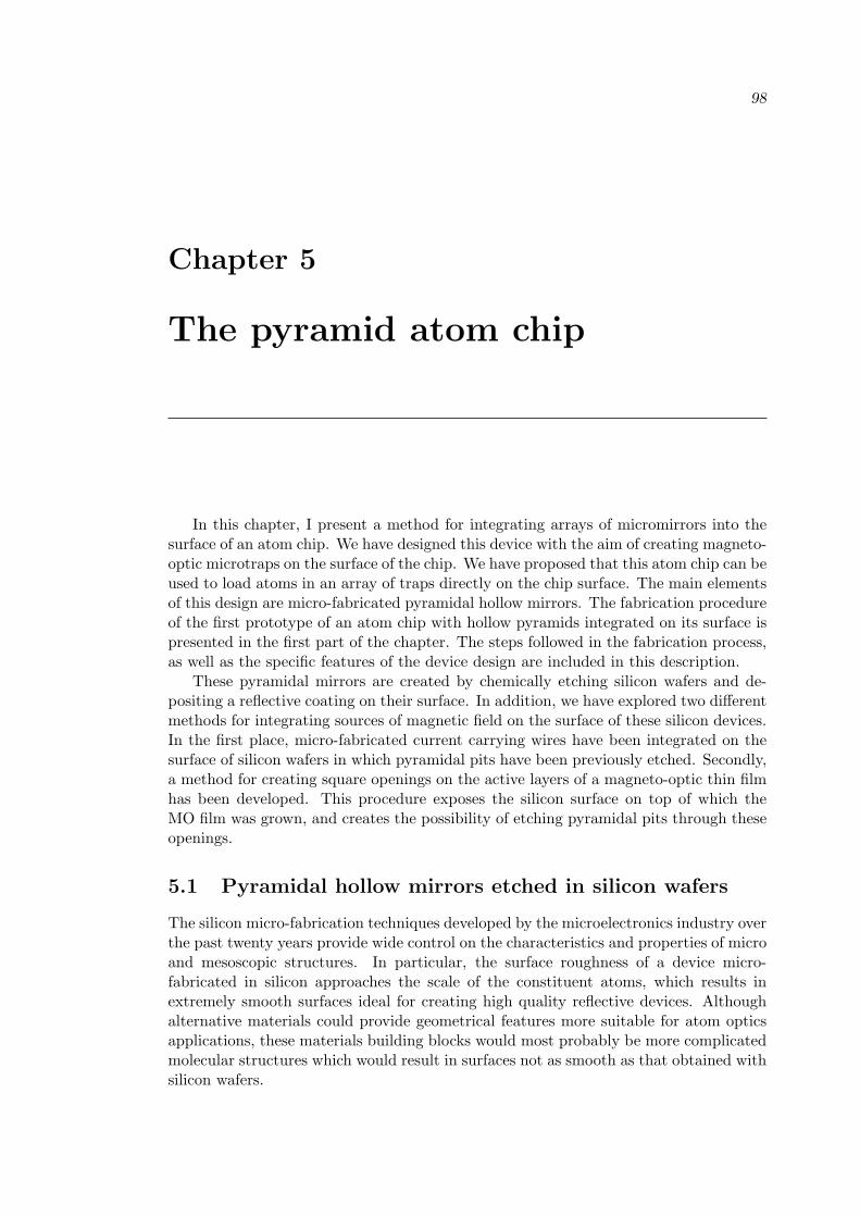
98
Chapter 5
The pyramid atom chip
In this chapter, I present a method for integrating arrays of micromirrors into thesurface of an atom chip. We have designed this device with the aim of creating magneto-optic microtraps on the surface of the chip. We have proposed that this atom chip can beused to load atoms in an array of traps directly on the chip surface. The main elementsof this design are micro-fabricated pyramidal hollow mirrors. The fabrication procedureof the first prototype of an atom chip with hollow pyramids integrated on its surface ispresented in the first part of the chapter. The steps followed in the fabrication process,as well as the specific features of the device design are included in this description.
These pyramidal mirrors are created by chemically etching silicon wafers and de-positing a reflective coating on their surface. In addition, we have explored two di"erentmethods for integrating sources of magnetic field on the surface of these silicon devices.In the first place, micro-fabricated current carrying wires have been integrated on thesurface of silicon wafers in which pyramidal pits have been previously etched. Secondly,a method for creating square openings on the active layers of a magneto-optic thin filmhas been developed. This procedure exposes the silicon surface on top of which theMO film was grown, and creates the possibility of etching pyramidal pits through theseopenings.
5.1 Pyramidal hollow mirrors etched in silicon wafers
The silicon micro-fabrication techniques developed by the microelectronics industry overthe past twenty years provide wide control on the characteristics and properties of microand mesoscopic structures. In particular, the surface roughness of a device micro-fabricated in silicon approaches the scale of the constituent atoms, which results inextremely smooth surfaces ideal for creating high quality reflective devices. Althoughalternative materials could provide geometrical features more suitable for atom opticsapplications, these materials building blocks would most probably be more complicatedmolecular structures which would result in surfaces not as smooth as that obtained withsilicon wafers.
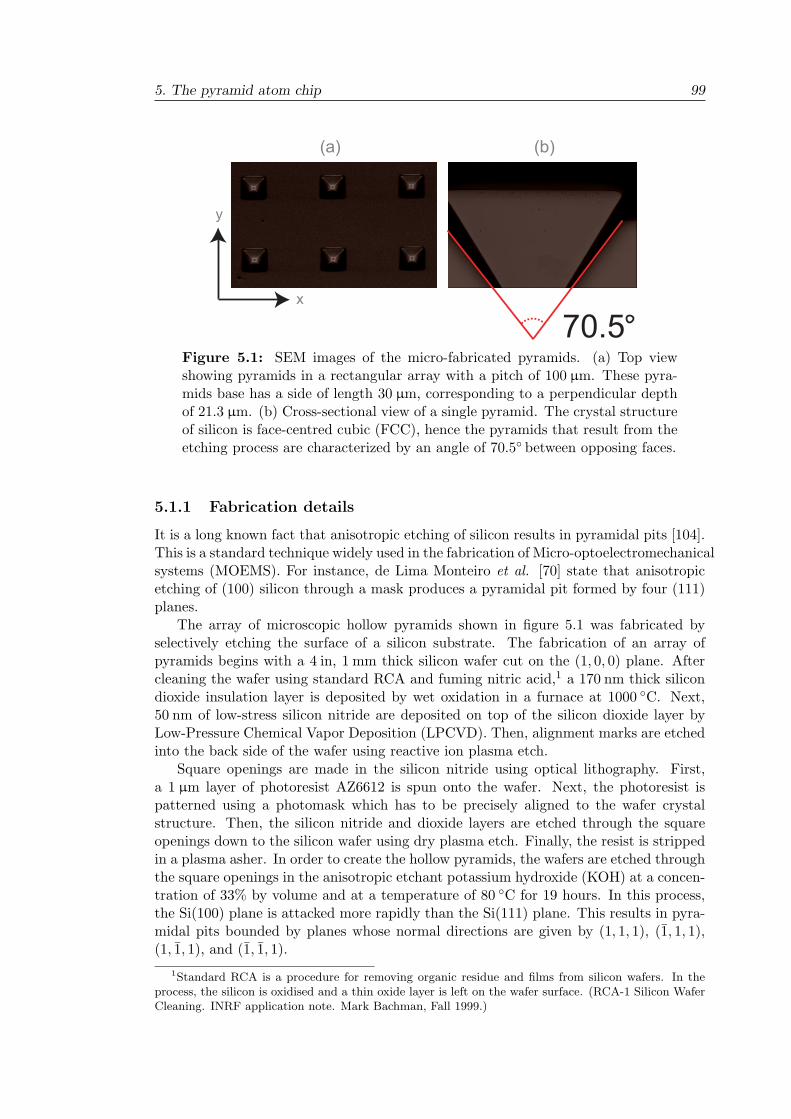
5. The pyramid atom chip 99
(b)(a)
y
x
Figure 5.1: SEM images of the micro-fabricated pyramids. (a) Top viewshowing pyramids in a rectangular array with a pitch of 100 µm. These pyra-mids base has a side of length 30 µm, corresponding to a perpendicular depthof 21.3 µm. (b) Cross-sectional view of a single pyramid. The crystal structureof silicon is face-centred cubic (FCC), hence the pyramids that result from theetching process are characterized by an angle of 70.5! between opposing faces.
5.1.1 Fabrication details
It is a long known fact that anisotropic etching of silicon results in pyramidal pits [104].This is a standard technique widely used in the fabrication of Micro-optoelectromechanicalsystems (MOEMS). For instance, de Lima Monteiro et al. [70] state that anisotropicetching of (100) silicon through a mask produces a pyramidal pit formed by four (111)planes.
The array of microscopic hollow pyramids shown in figure 5.1 was fabricated byselectively etching the surface of a silicon substrate. The fabrication of an array ofpyramids begins with a 4 in, 1 mm thick silicon wafer cut on the (1, 0, 0) plane. Aftercleaning the wafer using standard RCA and fuming nitric acid,1 a 170 nm thick silicondioxide insulation layer is deposited by wet oxidation in a furnace at 1000 !C. Next,50 nm of low-stress silicon nitride are deposited on top of the silicon dioxide layer byLow-Pressure Chemical Vapor Deposition (LPCVD). Then, alignment marks are etchedinto the back side of the wafer using reactive ion plasma etch.
Square openings are made in the silicon nitride using optical lithography. First,a 1 µm layer of photoresist AZ6612 is spun onto the wafer. Next, the photoresist ispatterned using a photomask which has to be precisely aligned to the wafer crystalstructure. Then, the silicon nitride and dioxide layers are etched through the squareopenings down to the silicon wafer using dry plasma etch. Finally, the resist is strippedin a plasma asher. In order to create the hollow pyramids, the wafers are etched throughthe square openings in the anisotropic etchant potassium hydroxide (KOH) at a concen-tration of 33% by volume and at a temperature of 80 !C for 19 hours. In this process,the Si(100) plane is attacked more rapidly than the Si(111) plane. This results in pyra-midal pits bounded by planes whose normal directions are given by (1, 1, 1), (1, 1, 1),(1, 1, 1), and (1, 1, 1).
1Standard RCA is a procedure for removing organic residue and films from silicon wafers. In theprocess, the silicon is oxidised and a thin oxide layer is left on the wafer surface. (RCA-1 Silicon WaferCleaning. INRF application note. Mark Bachman, Fall 1999.)
5. The pyramid atom chip 100
12
12
3
12
3
Type 1
Type 2
Type 3
Si AuType 1 Type 2 Type 3
(a) (b) (c) (d)
Figure 5.2: In (a), The reflection areas were each one of the three ray types areproduced are shown in a top view of the pyramid. (b), (c), and (d) representexamples of the paths followed by these rays, which are sketched in a crosssection of the pyramid.
The oxide layer is then stripped away and finally a metallic reflective layer is sput-tered on the sample. As gold is a good reflector for infrared (IR) light (see table 3.1),a 5 nm adhesion chromium layer and a 100 nm gold layer were sputtered on top of apyramids array sample. In conclusion, an array of hollow pyramidal highly reflectivemirrors has been fabricated on the surface of a silicon wafer. The next step of thisproject was therefore to determine the optical properties of these mirrors.
5.1.2 Geometrical characteristics
The angle between the opposing faces of the pyramids etched in silicon can be easilycalculated. Take for example the {1, 1, 1} and the {1, 1, 1} planes of the silicon crystal.The angle - between the two vectors (1, 1, 1) and ("1,"1, 1) is given by:
(1, 1, 1) · ("1,"1, 1) = (%
3)2 cos -.
Therefore- = cos"1
11/3
2* 70.53!, (5.1)
which is the value quoted in figure 5.1. This is also the apex angle of the pyramidstudied in chapter 4.
5.1.3 Optical properties
With respect to the optical reflections that these pyramids generate, their surface can beseparated into three regions, schematically represented in figure 5.2(a). A ray parallel tothe axis of the pyramid is first reflected at the point marked 1!in diagrams (b),(c) and(d). It then travels along a diagonal line which points down to the pyramid apex andtowards the opposite pyramid face. The propagation direction after the first reflectionmakes an angle of &"- with the pyramid axis. Light that is first reflected in the middleof a pyramid face travels through the pyramid internal volume and reaches the oppositeface. These rays are reflected a second time, as represented by points 2!in diagrams(b) and (c). The direction of propagation after this second reflection is also diagonallyoriented, but this time it points away from the pyramid apex. This new directionmakes an angle of & " 2- with the pyramid axis. This angle is bigger than the 35.25!
5. The pyramid atom chip 101
angle between the pyramid faces and axis. Consequently, the ray has to intersect theplane defined by the pyramid face at some point. Beams that follow this two reflectionpattern and leave the pyramid without su"ering a third reflection have been denoted astype 1 reflections (diagram (b)). When there is a third reflection inside the pyramid,as shown in diagram (c), the ray is denoted as type 2. Only the central region of theincoming beam, the one that is firstly reflected near the pyramid apex, gives rise to type2 reflections. Rays initially reflected close to the pyramid edges intersect the adjacentpyramid face before reaching the opposite one. The path followed by such ray, calledtype 3, is represented in diagram (d). The second reflection, point 2!in this diagram,is on the adjacent mirror. After the third reflection, which is shown as point 3!, theserays finally leave the pyramid volume, crossing through the pyramid axis at an angle of31.59!.
Type 1 and 2 reflections
A ray contained in the section of light that makes up a type 1 or a type 2 reflectionremains in its initial plane of incidence. The incident light propagates parallel to thepyramid axis. Consequently, an incident ray makes an angle of -/2 = 1
2 cos"1(1/3)with the pyramid face and the angle of incidence is &/2" -/2 = 1
2 (& " -). This firstlyreflected section of light crosses through the pyramid internal volume making an angleof &"- with a vector pointing out of the pyramid and along its axis. A ray that crossesthrough the pyramid axis forms a triangle with the lines generated by the intersectionsof the pyramid faces and the plane of incidence. In consequence, the angle this raymakes with the pyramid face in which the second reflection is produced is & " 3
2-.Correspondingly, the second reflection angle of incidence turns out to be 1
2 (3- " &). Anew triangle can now be used to deduce the angle that this secondly reflected ray makeswith the pyramid axis. This time, the sides of this triangle are formed by the pyramidaxis, the pyramid face in which the second reflection was produced, and the secondlyreflected ray itself. From these considerations we conclude that the secondly reflectedray makes an angle of & " 2- with the pyramid axis.
Type 3 reflections
In contrast to what happens in a 90! pyramid, after the first reflection into the pyramid,light travels diagonally towards the pyramid apex. Because of this, some light intersectsthe pyramid face that is adjacent to that of the first reflection. The normal to this newreflection plane is not longer parallel to the plane defined by the first reflection. Thiscomplicates the derivation from simple geometrical arguments of the second reflectionangle of incidence. However, a ray tracing analysis of the pyramid allows us to calculateboth the incidence angles and the angles at which type 3 reflections cross the pyramidaxis. The angle of incidence at the second reflection has been calculated to be 78.9!,while for the third reflection the angle of incidence is 33.49!. After su"ering this thirdreflection, a type 3 ray escapes the pyramid crossing through its axis at an angle of31.59!.
The reflected light intensity distribution
The first test we made on an array of pyramidal micromirrors, (see figure 5.1) consistedof shining a collimated 1 mm-diameter laser beam on the surface of an array pyramidal
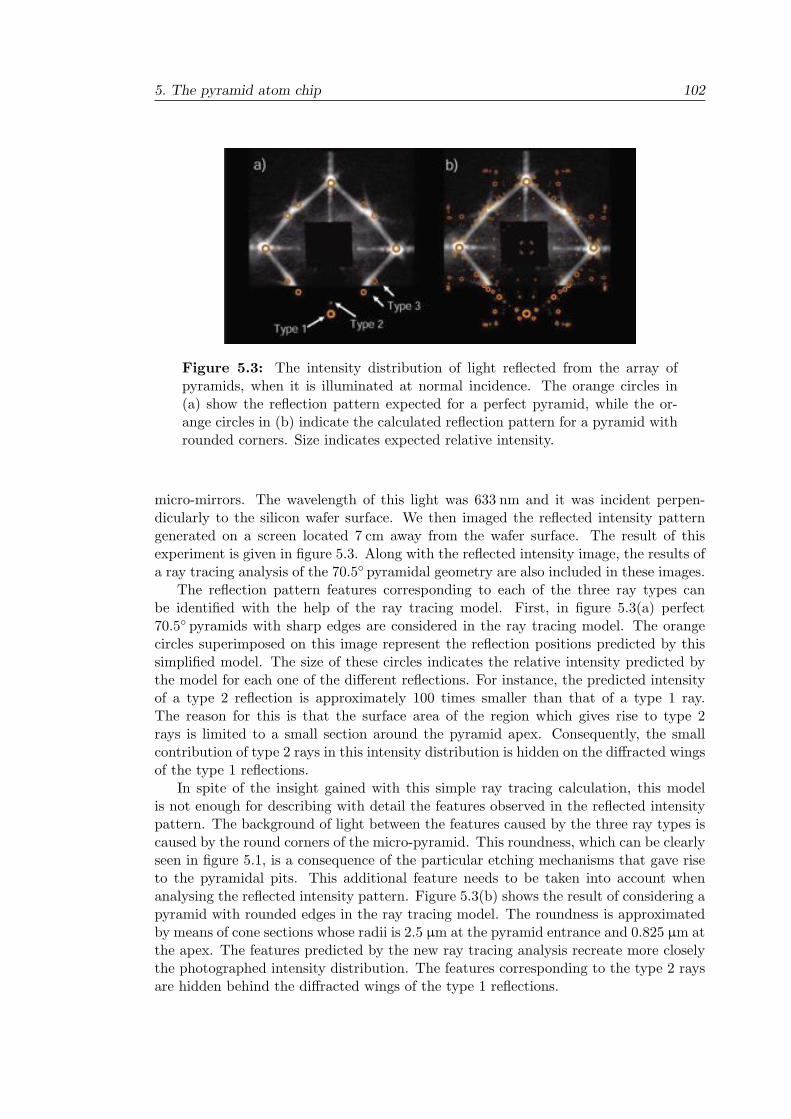
5. The pyramid atom chip 102
Figure 5.3: The intensity distribution of light reflected from the array ofpyramids, when it is illuminated at normal incidence. The orange circles in(a) show the reflection pattern expected for a perfect pyramid, while the or-ange circles in (b) indicate the calculated reflection pattern for a pyramid withrounded corners. Size indicates expected relative intensity.
micro-mirrors. The wavelength of this light was 633 nm and it was incident perpen-dicularly to the silicon wafer surface. We then imaged the reflected intensity patterngenerated on a screen located 7 cm away from the wafer surface. The result of thisexperiment is given in figure 5.3. Along with the reflected intensity image, the results ofa ray tracing analysis of the 70.5! pyramidal geometry are also included in these images.
The reflection pattern features corresponding to each of the three ray types canbe identified with the help of the ray tracing model. First, in figure 5.3(a) perfect70.5! pyramids with sharp edges are considered in the ray tracing model. The orangecircles superimposed on this image represent the reflection positions predicted by thissimplified model. The size of these circles indicates the relative intensity predicted bythe model for each one of the di"erent reflections. For instance, the predicted intensityof a type 2 reflection is approximately 100 times smaller than that of a type 1 ray.The reason for this is that the surface area of the region which gives rise to type 2rays is limited to a small section around the pyramid apex. Consequently, the smallcontribution of type 2 rays in this intensity distribution is hidden on the di"racted wingsof the type 1 reflections.
In spite of the insight gained with this simple ray tracing calculation, this modelis not enough for describing with detail the features observed in the reflected intensitypattern. The background of light between the features caused by the three ray types iscaused by the round corners of the micro-pyramid. This roundness, which can be clearlyseen in figure 5.1, is a consequence of the particular etching mechanisms that gave riseto the pyramidal pits. This additional feature needs to be taken into account whenanalysing the reflected intensity pattern. Figure 5.3(b) shows the result of considering apyramid with rounded edges in the ray tracing model. The roundness is approximatedby means of cone sections whose radii is 2.5 µm at the pyramid entrance and 0.825 µm atthe apex. The features predicted by the new ray tracing analysis recreate more closelythe photographed intensity distribution. The features corresponding to the type 2 raysare hidden behind the di"racted wings of the type 1 reflections.
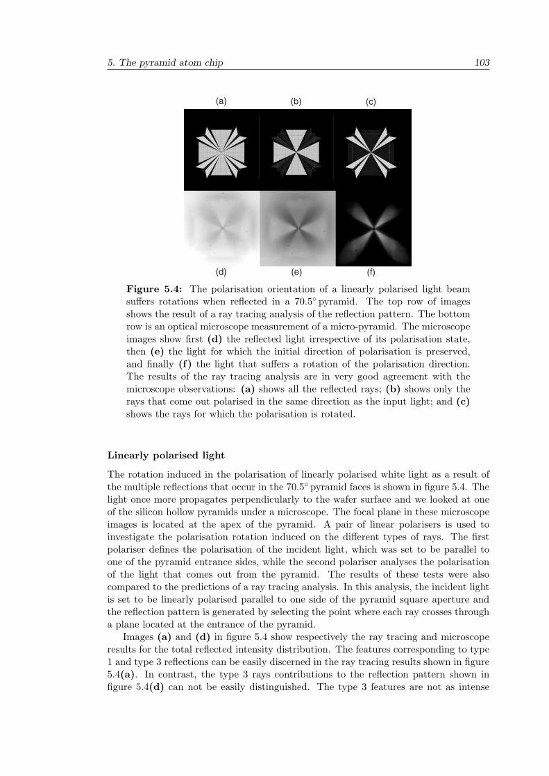
5. The pyramid atom chip 103
(a)
(e)
(b) (c)
(d) (f)
Figure 5.4: The polarisation orientation of a linearly polarised light beamsu"ers rotations when reflected in a 70.5! pyramid. The top row of imagesshows the result of a ray tracing analysis of the reflection pattern. The bottomrow is an optical microscope measurement of a micro-pyramid. The microscopeimages show first (d) the reflected light irrespective of its polarisation state,then (e) the light for which the initial direction of polarisation is preserved,and finally (f) the light that su"ers a rotation of the polarisation direction.The results of the ray tracing analysis are in very good agreement with themicroscope observations: (a) shows all the reflected rays; (b) shows only therays that come out polarised in the same direction as the input light; and (c)shows the rays for which the polarisation is rotated.
Linearly polarised light
The rotation induced in the polarisation of linearly polarised white light as a result ofthe multiple reflections that occur in the 70.5! pyramid faces is shown in figure 5.4. Thelight once more propagates perpendicularly to the wafer surface and we looked at oneof the silicon hollow pyramids under a microscope. The focal plane in these microscopeimages is located at the apex of the pyramid. A pair of linear polarisers is used toinvestigate the polarisation rotation induced on the di"erent types of rays. The firstpolariser defines the polarisation of the incident light, which was set to be parallel toone of the pyramid entrance sides, while the second polariser analyses the polarisationof the light that comes out from the pyramid. The results of these tests were alsocompared to the predictions of a ray tracing analysis. In this analysis, the incident lightis set to be linearly polarised parallel to one side of the pyramid square aperture andthe reflection pattern is generated by selecting the point where each ray crosses througha plane located at the entrance of the pyramid.
Images (a) and (d) in figure 5.4 show respectively the ray tracing and microscoperesults for the total reflected intensity distribution. The features corresponding to type1 and type 3 reflections can be easily discerned in the ray tracing results shown in figure5.4(a). In contrast, the type 3 rays contributions to the reflection pattern shown infigure 5.4(d) can not be easily distinguished. The type 3 features are not as intense
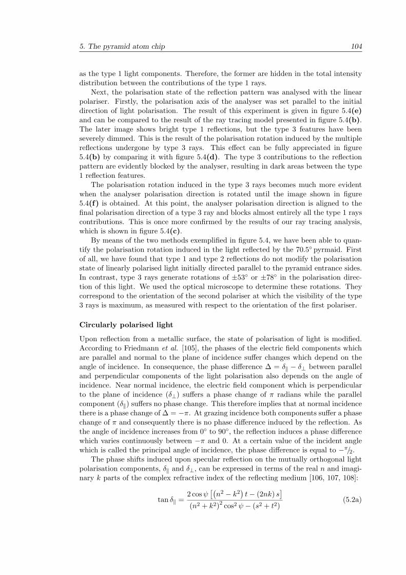
5. The pyramid atom chip 104
as the type 1 light components. Therefore, the former are hidden in the total intensitydistribution between the contributions of the type 1 rays.
Next, the polarisation state of the reflection pattern was analysed with the linearpolariser. Firstly, the polarisation axis of the analyser was set parallel to the initialdirection of light polarisation. The result of this experiment is given in figure 5.4(e)and can be compared to the result of the ray tracing model presented in figure 5.4(b).The later image shows bright type 1 reflections, but the type 3 features have beenseverely dimmed. This is the result of the polarisation rotation induced by the multiplereflections undergone by type 3 rays. This e"ect can be fully appreciated in figure5.4(b) by comparing it with figure 5.4(d). The type 3 contributions to the reflectionpattern are evidently blocked by the analyser, resulting in dark areas between the type1 reflection features.
The polarisation rotation induced in the type 3 rays becomes much more evidentwhen the analyser polarisation direction is rotated until the image shown in figure5.4(f) is obtained. At this point, the analyser polarisation direction is aligned to thefinal polarisation direction of a type 3 ray and blocks almost entirely all the type 1 rayscontributions. This is once more confirmed by the results of our ray tracing analysis,which is shown in figure 5.4(c).
By means of the two methods exemplified in figure 5.4, we have been able to quan-tify the polarisation rotation induced in the light reflected by the 70.5! pyrmaid. Firstof all, we have found that type 1 and type 2 reflections do not modify the polarisationstate of linearly polarised light initially directed parallel to the pyramid entrance sides.In contrast, type 3 rays generate rotations of ±53! or ±78! in the polarisation direc-tion of this light. We used the optical microscope to determine these rotations. Theycorrespond to the orientation of the second polariser at which the visibility of the type3 rays is maximum, as measured with respect to the orientation of the first polariser.
Circularly polarised light
Upon reflection from a metallic surface, the state of polarisation of light is modified.According to Friedmann et al. [105], the phases of the electric field components whichare parallel and normal to the plane of incidence su"er changes which depend on theangle of incidence. In consequence, the phase di"erence $ = *& " *' between paralleland perpendicular components of the light polarisation also depends on the angle ofincidence. Near normal incidence, the electric field component which is perpendicularto the plane of incidence (*') su"ers a phase change of & radians while the parallelcomponent (*&) su"ers no phase change. This therefore implies that at normal incidencethere is a phase change of $ = "&. At grazing incidence both components su"er a phasechange of & and consequently there is no phase di"erence induced by the reflection. Asthe angle of incidence increases from 0! to 90!, the reflection induces a phase di"erencewhich varies continuously between "& and 0. At a certain value of the incident anglewhich is called the principal angle of incidence, the phase di"erence is equal to "!/2.
The phase shifts induced upon specular reflection on the mutually orthogonal lightpolarisation components, *& and *', can be expressed in terms of the real n and imagi-nary k parts of the complex refractive index of the reflecting medium [106, 107, 108]:
tan *& =2 cos 1
61n2 " k2
2t" (2nk) s
7
(n2 + k2)2 cos2 1 " (s2 + t2)(5.2a)
5. The pyramid atom chip 105
tan *' =2t cos 1
cos2 1 " (s2 + t2)(5.2b)
where2s2 =
31n2 " k2 " sin2 1
22 + 4n2k2 +1n2 " k2 " sin2 1
2(5.3a)
2t2 =31
n2 " k2 " sin2 122 + 4n2k2 "
1n2 " k2 " sin2 1
2(5.3b)
With the aim of confirming this information and characterising the metallic mirrorsfabricated in the Centre for Cold Matter, we made a measurement of the retardationinduced between the two mutually orthogonal components of a circularly polarised laserbeam upon reflection from a gold mirror. The mirror utilised in this experiment wasfabricated by sputter deposition of the metallic material on the surface of a glass slide.To begin with, a thin chromium adhesion layer (5 nm) was laid on the surface of theglass slide. Then, an optically thick 100 nm layer of gold was sputtered on top of thechromium layer. This is the standard method used in our laboratory for fabricatinggold mirrors and results in highly reflective (! 95%) surfaces for infrared light.
In this experiment, a circularly polarised beam was reflected by the gold mirrorand the reflected beam was analysed by means of a quarter wave plate and a linearpolariser. The procedure was repeated for various angles of incidence. A laser beam ina linear horizontal polarisation state was firstly obtained by taking the light transmittedthrough a polarising beam cube. The circular polarisation was next prepared by sendingthe horizontally polarised light beam through a quarter wave plate whose fast axis wasoriented at an angle of 45! with respect to the initial light polarisation state. Thiscircularly polarised light beam was then reflected by the gold mirror, which was held ona mount that allowed us to vary the angle of incidence 1. Finally, the reflected beamwas sent through a second quarter wave plate and a horizontal linear polariser beforereaching a detector in which the transmitted power was measured. For a given angle ofincidence, the polarisation state of the reflected light can be determined by measuringthe dependence between the power transmitted through the linear polariser and theorientation of the second quarter wave plate.
Using the Jones Matrix formalism, the polarisation state of the beam before thereflection is given by [100]:
JI =1%2
)12
*
The e"ect that the mirror has on the polarisation state of the light can be expressedas a wave retarder having a fast axis parallel to the plane of incidence. This way, thepolarisation state of the light after the reflection can be expressed in the following way:
JR(/) = TM (/) ·JI = e".+/2
)1 00 e.+
*· 1%
2
)12
*=
e".+/2
%2
)1
2e.+
*
Next, the polarisation state of the reflected beam is interrogated by means of aquarter wave plate T"/4 and a horizontal linear polariser Tlh
JE(/, -) = Tlh ·T"/4(-) ·JR
whereTlh =
)10
*
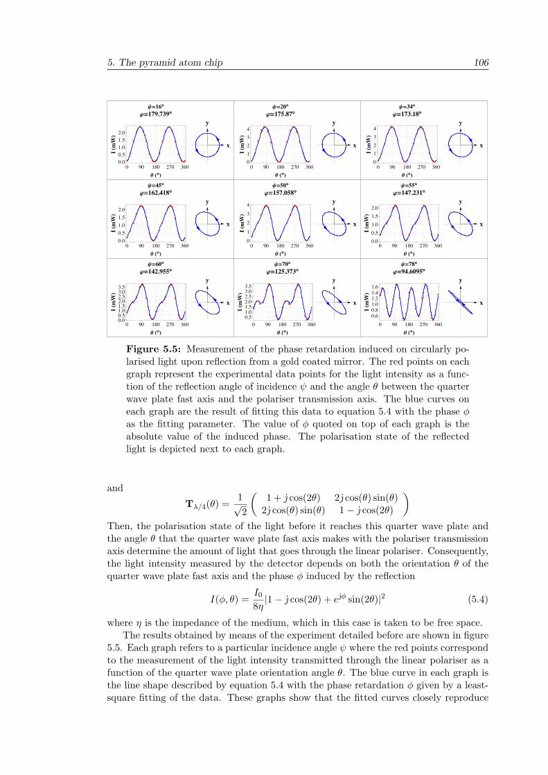
5. The pyramid atom chip 106
0 90 180 270 3600.00.51.01.52.0
! !""
I!mW"
#$16"%$179.739"
x
y
0 90 180 270 36001234
! !""
I!mW"
#$20"%$175.87"
x
y
0 90 180 270 36001234
! !""
I!mW"
#$34"%$173.18"
x
y
0 90 180 270 3600.00.51.01.52.0
! !""
I!mW"
#$45"%$162.418"
x
y
0 90 180 270 3600
1
2
3
4
! !""I!mW
"
#$50"%$157.058"
x
y
0 90 180 270 3600.00.51.01.52.0
! !""
I!mW"
#$55"%$147.231"
x
y
0 90 180 270 3600.00.51.01.52.02.53.03.5
! !""
I!mW"
#$60"%$142.955"
x
y
0 90 180 270 3600.51.01.52.02.53.03.5
! !""
I!mW"
#$70"%$125.373"
x
y
0 90 180 270 3600.60.81.01.21.41.6
! !""
I!mW"
#$78"%$94.6095"
x
y
Figure 5.5: Measurement of the phase retardation induced on circularly po-larised light upon reflection from a gold coated mirror. The red points on eachgraph represent the experimental data points for the light intensity as a func-tion of the reflection angle of incidence 1 and the angle - between the quarterwave plate fast axis and the polariser transmission axis. The blue curves oneach graph are the result of fitting this data to equation 5.4 with the phase /as the fitting parameter. The value of / quoted on top of each graph is theabsolute value of the induced phase. The polarisation state of the reflectedlight is depicted next to each graph.
andT"/4(-) =
1%2
)1 + 2 cos(2-) 22 cos(-) sin(-)
22 cos(-) sin(-) 1" 2 cos(2-)
*
Then, the polarisation state of the light before it reaches this quarter wave plate andthe angle - that the quarter wave plate fast axis makes with the polariser transmissionaxis determine the amount of light that goes through the linear polariser. Consequently,the light intensity measured by the detector depends on both the orientation - of thequarter wave plate fast axis and the phase / induced by the reflection
I(/, -) =I0
8.|1" 2 cos(2-) + e.+ sin(2-)|2 (5.4)
where . is the impedance of the medium, which in this case is taken to be free space.The results obtained by means of the experiment detailed before are shown in figure
5.5. Each graph refers to a particular incidence angle 1 where the red points correspondto the measurement of the light intensity transmitted through the linear polariser as afunction of the quarter wave plate orientation angle -. The blue curve in each graph isthe line shape described by equation 5.4 with the phase retardation / given by a least-square fitting of the data. These graphs show that the fitted curves closely reproduce
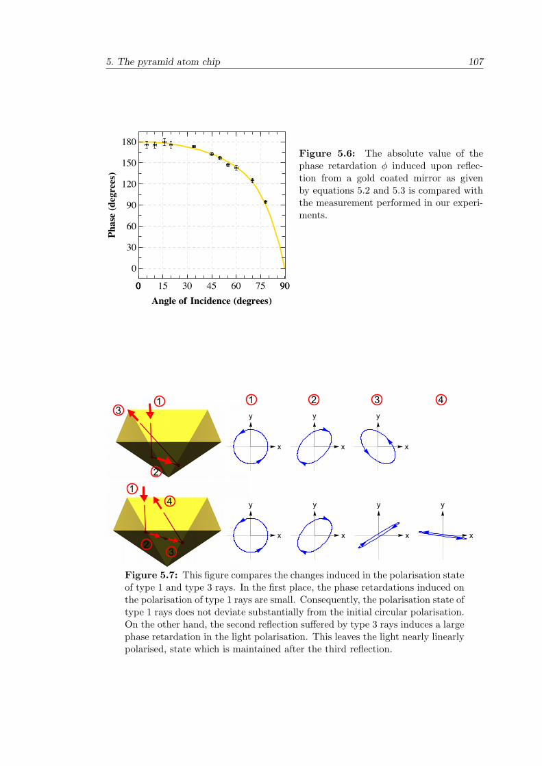
5. The pyramid atom chip 107
000 90900 15 30 45 60 75
0
30
60
90
120
150
180
Angle of Incidence !degrees"
Phase!degr
ees"
Figure 5.6: The absolute value of thephase retardation / induced upon reflec-tion from a gold coated mirror as givenby equations 5.2 and 5.3 is compared withthe measurement performed in our experi-ments.
Figure 5.7: This figure compares the changes induced in the polarisation stateof type 1 and type 3 rays. In the first place, the phase retardations induced onthe polarisation of type 1 rays are small. Consequently, the polarisation state oftype 1 rays does not deviate substantially from the initial circular polarisation.On the other hand, the second reflection su"ered by type 3 rays induces a largephase retardation in the light polarisation. This leaves the light nearly linearlypolarised, state which is maintained after the third reflection.
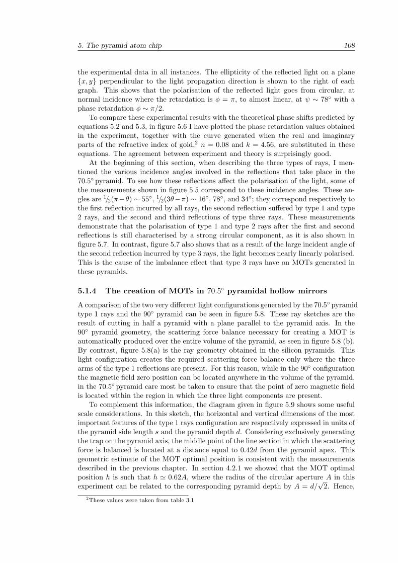
5. The pyramid atom chip 108
the experimental data in all instances. The ellipticity of the reflected light on a plane{x, y} perpendicular to the light propagation direction is shown to the right of eachgraph. This shows that the polarisation of the reflected light goes from circular, atnormal incidence where the retardation is / = &, to almost linear, at 1 ! 78! with aphase retardation / ! &/2.
To compare these experimental results with the theoretical phase shifts predicted byequations 5.2 and 5.3, in figure 5.6 I have plotted the phase retardation values obtainedin the experiment, together with the curve generated when the real and imaginaryparts of the refractive index of gold,2 n = 0.08 and k = 4.56, are substituted in theseequations. The agreement between experiment and theory is surprisingly good.
At the beginning of this section, when describing the three types of rays, I men-tioned the various incidence angles involved in the reflections that take place in the70.5! pyramid. To see how these reflections a"ect the polarisation of the light, some ofthe measurements shown in figure 5.5 correspond to these incidence angles. These an-gles are 1/2(&"-) ! 55!, 1/2(3-"&) ! 16!, 78!, and 34!; they correspond respectively tothe first reflection incurred by all rays, the second reflection su"ered by type 1 and type2 rays, and the second and third reflections of type three rays. These measurementsdemonstrate that the polarisation of type 1 and type 2 rays after the first and secondreflections is still characterised by a strong circular component, as it is also shown infigure 5.7. In contrast, figure 5.7 also shows that as a result of the large incident angle ofthe second reflection incurred by type 3 rays, the light becomes nearly linearly polarised.This is the cause of the imbalance e"ect that type 3 rays have on MOTs generated inthese pyramids.
5.1.4 The creation of MOTs in 70.5! pyramidal hollow mirrors
A comparison of the two very di"erent light configurations generated by the 70.5! pyramidtype 1 rays and the 90! pyramid can be seen in figure 5.8. These ray sketches are theresult of cutting in half a pyramid with a plane parallel to the pyramid axis. In the90! pyramid geometry, the scattering force balance necessary for creating a MOT isautomatically produced over the entire volume of the pyramid, as seen in figure 5.8 (b).By contrast, figure 5.8(a) is the ray geometry obtained in the silicon pyramids. Thislight configuration creates the required scattering force balance only where the threearms of the type 1 reflections are present. For this reason, while in the 90! configurationthe magnetic field zero position can be located anywhere in the volume of the pyramid,in the 70.5! pyramid care most be taken to ensure that the point of zero magnetic fieldis located within the region in which the three light components are present.
To complement this information, the diagram given in figure 5.9 shows some usefulscale considerations. In this sketch, the horizontal and vertical dimensions of the mostimportant features of the type 1 rays configuration are respectively expressed in units ofthe pyramid side length s and the pyramid depth d. Considering exclusively generatingthe trap on the pyramid axis, the middle point of the line section in which the scatteringforce is balanced is located at a distance equal to 0.42d from the pyramid apex. Thisgeometric estimate of the MOT optimal position is consistent with the measurementsdescribed in the previous chapter. In section 4.2.1 we showed that the MOT optimalposition h is such that h + 0.62A, where the radius of the circular aperture A in thisexperiment can be related to the corresponding pyramid depth by A = d/
%2. Hence,
2These values were taken from table 3.1
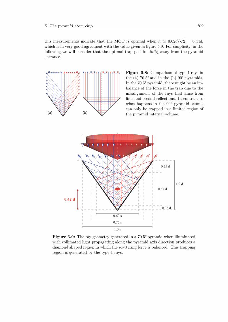
5. The pyramid atom chip 109
this measurements indicate that the MOT is optimal when h + 0.62d/%
2 = 0.44d,which is in very good agreement with the value given in figure 5.9. For simplicity, in thefollowing we will consider that the optimal trap position is d/2 away from the pyramidentrance.
(b)(a)
Figure 5.8: Comparison of type 1 rays inthe (a) 70.5! and in the (b) 90! pyramids.In the 70.5! pyramid, there might be an im-balance of the force in the trap due to themisalignment of the rays that arise fromfirst and second reflections. In contrast towhat happens in the 90! pyramid, atomscan only be trapped in a limited region ofthe pyramid internal volume.
0.08 d
1.0 d0.67 d
0.25 d
0.42 d
1.0 s
0.75 s
0.60 s
Figure 5.9: The ray geometry generated in a 70.5! pyramid when illuminatedwith collimated light propagating along the pyramid axis direction produces adiamond shaped region in which the scattering force is balanced. This trappingregion is generated by the type 1 rays.
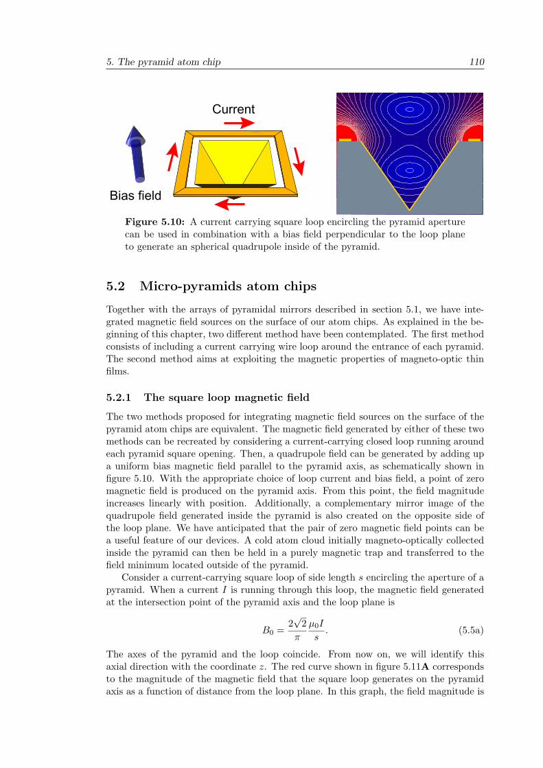
5. The pyramid atom chip 110
Current
Bias field
Figure 5.10: A current carrying square loop encircling the pyramid aperturecan be used in combination with a bias field perpendicular to the loop planeto generate an spherical quadrupole inside of the pyramid.
5.2 Micro-pyramids atom chips
Together with the arrays of pyramidal mirrors described in section 5.1, we have inte-grated magnetic field sources on the surface of our atom chips. As explained in the be-ginning of this chapter, two di"erent method have been contemplated. The first methodconsists of including a current carrying wire loop around the entrance of each pyramid.The second method aims at exploiting the magnetic properties of magneto-optic thinfilms.
5.2.1 The square loop magnetic field
The two methods proposed for integrating magnetic field sources on the surface of thepyramid atom chips are equivalent. The magnetic field generated by either of these twomethods can be recreated by considering a current-carrying closed loop running aroundeach pyramid square opening. Then, a quadrupole field can be generated by adding upa uniform bias magnetic field parallel to the pyramid axis, as schematically shown infigure 5.10. With the appropriate choice of loop current and bias field, a point of zeromagnetic field is produced on the pyramid axis. From this point, the field magnitudeincreases linearly with position. Additionally, a complementary mirror image of thequadrupole field generated inside the pyramid is also created on the opposite side ofthe loop plane. We have anticipated that the pair of zero magnetic field points can bea useful feature of our devices. A cold atom cloud initially magneto-optically collectedinside the pyramid can then be held in a purely magnetic trap and transferred to thefield minimum located outside of the pyramid.
Consider a current-carrying square loop of side length s encircling the aperture of apyramid. When a current I is running through this loop, the magnetic field generatedat the intersection point of the pyramid axis and the loop plane is
B0 =2%
2&
µ0I
s. (5.5a)
The axes of the pyramid and the loop coincide. From now on, we will identify thisaxial direction with the coordinate z. The red curve shown in figure 5.11A correspondsto the magnitude of the magnetic field that the square loop generates on the pyramidaxis as a function of distance from the loop plane. In this graph, the field magnitude is
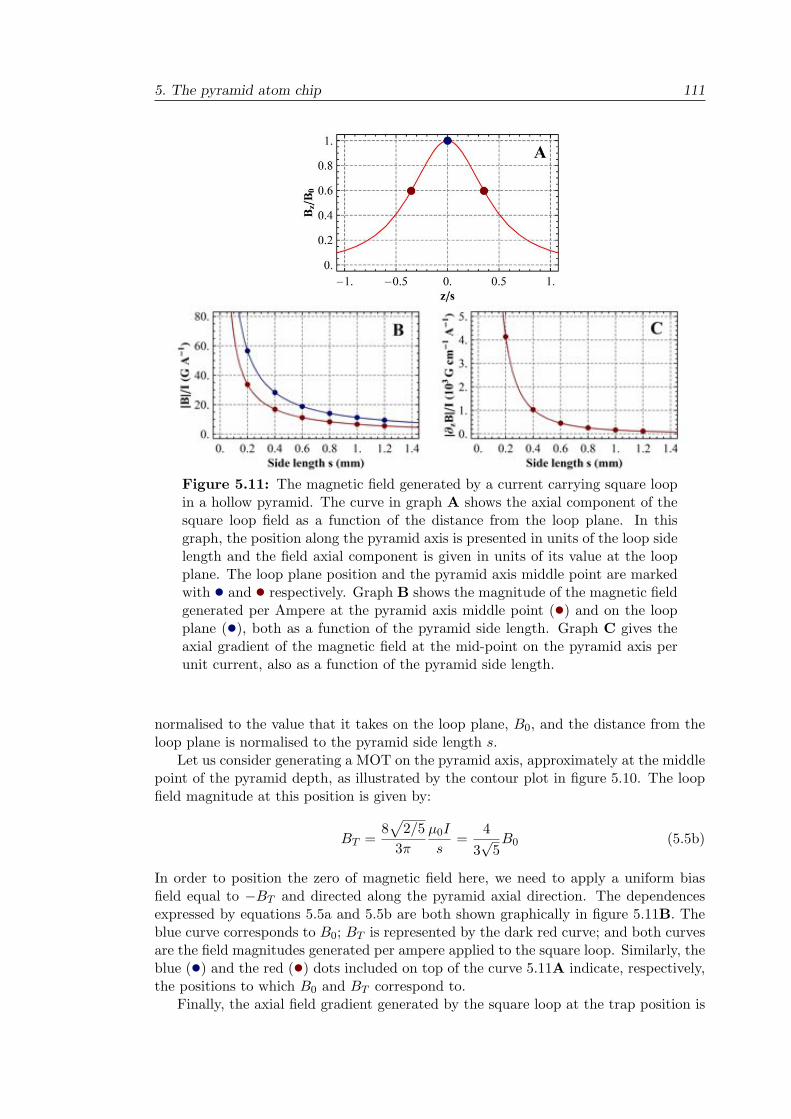
5. The pyramid atom chip 111
Figure 5.11: The magnetic field generated by a current carrying square loopin a hollow pyramid. The curve in graph A shows the axial component of thesquare loop field as a function of the distance from the loop plane. In thisgraph, the position along the pyramid axis is presented in units of the loop sidelength and the field axial component is given in units of its value at the loopplane. The loop plane position and the pyramid axis middle point are markedwith • and • respectively. Graph B shows the magnitude of the magnetic fieldgenerated per Ampere at the pyramid axis middle point (•) and on the loopplane (•), both as a function of the pyramid side length. Graph C gives theaxial gradient of the magnetic field at the mid-point on the pyramid axis perunit current, also as a function of the pyramid side length.
normalised to the value that it takes on the loop plane, B0, and the distance from theloop plane is normalised to the pyramid side length s.
Let us consider generating a MOT on the pyramid axis, approximately at the middlepoint of the pyramid depth, as illustrated by the contour plot in figure 5.10. The loopfield magnitude at this position is given by:
BT =8(
2/53&
µ0I
s=
43%
5B0 (5.5b)
In order to position the zero of magnetic field here, we need to apply a uniform biasfield equal to "BT and directed along the pyramid axial direction. The dependencesexpressed by equations 5.5a and 5.5b are both shown graphically in figure 5.11B. Theblue curve corresponds to B0; BT is represented by the dark red curve; and both curvesare the field magnitudes generated per ampere applied to the square loop. Similarly, theblue (•) and the red (•) dots included on top of the curve 5.11A indicate, respectively,the positions to which B0 and BT correspond to.
Finally, the axial field gradient generated by the square loop at the trap position is
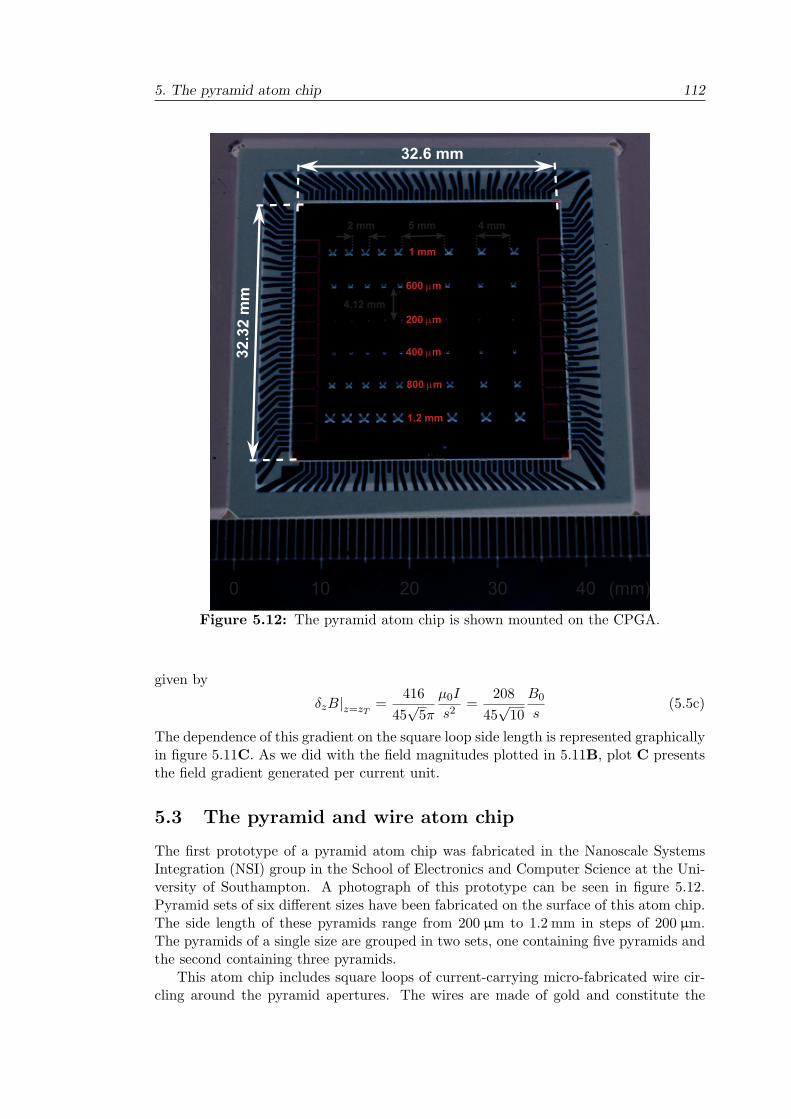
5. The pyramid atom chip 112
0 20 30 4010
32.6 mm
32.3
2 m
m5 mm2 mm 4 mm
4.12 mm
1 mm
800 µm
1.2 mm
600 µm
200 µm
400 µm
(mm)Figure 5.12: The pyramid atom chip is shown mounted on the CPGA.
given by
*zB|z=zT=
41645%
5&
µ0I
s2=
20845%
10B0
s(5.5c)
The dependence of this gradient on the square loop side length is represented graphicallyin figure 5.11C. As we did with the field magnitudes plotted in 5.11B, plot C presentsthe field gradient generated per current unit.
5.3 The pyramid and wire atom chip
The first prototype of a pyramid atom chip was fabricated in the Nanoscale SystemsIntegration (NSI) group in the School of Electronics and Computer Science at the Uni-versity of Southampton. A photograph of this prototype can be seen in figure 5.12.Pyramid sets of six di"erent sizes have been fabricated on the surface of this atom chip.The side length of these pyramids range from 200 µm to 1.2 mm in steps of 200 µm.The pyramids of a single size are grouped in two sets, one containing five pyramids andthe second containing three pyramids.
This atom chip includes square loops of current-carrying micro-fabricated wire cir-cling around the pyramid apertures. The wires are made of gold and constitute the
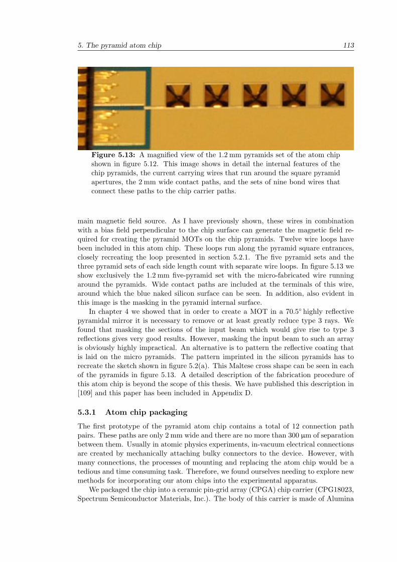
5. The pyramid atom chip 113
Figure 5.13: A magnified view of the 1.2 mm pyramids set of the atom chipshown in figure 5.12. This image shows in detail the internal features of thechip pyramids, the current carrying wires that run around the square pyramidapertures, the 2 mm wide contact paths, and the sets of nine bond wires thatconnect these paths to the chip carrier paths.
main magnetic field source. As I have previously shown, these wires in combinationwith a bias field perpendicular to the chip surface can generate the magnetic field re-quired for creating the pyramid MOTs on the chip pyramids. Twelve wire loops havebeen included in this atom chip. These loops run along the pyramid square entrances,closely recreating the loop presented in section 5.2.1. The five pyramid sets and thethree pyramid sets of each side length count with separate wire loops. In figure 5.13 weshow exclusively the 1.2 mm five-pyramid set with the micro-fabricated wire runningaround the pyramids. Wide contact paths are included at the terminals of this wire,around which the blue naked silicon surface can be seen. In addition, also evident inthis image is the masking in the pyramid internal surface.
In chapter 4 we showed that in order to create a MOT in a 70.5! highly reflectivepyramidal mirror it is necessary to remove or at least greatly reduce type 3 rays. Wefound that masking the sections of the input beam which would give rise to type 3reflections gives very good results. However, masking the input beam to such an arrayis obviously highly impractical. An alternative is to pattern the reflective coating thatis laid on the micro pyramids. The pattern imprinted in the silicon pyramids has torecreate the sketch shown in figure 5.2(a). This Maltese cross shape can be seen in eachof the pyramids in figure 5.13. A detailed description of the fabrication procedure ofthis atom chip is beyond the scope of this thesis. We have published this description in[109] and this paper has been included in Appendix D.
5.3.1 Atom chip packaging
The first prototype of the pyramid atom chip contains a total of 12 connection pathpairs. These paths are only 2 mm wide and there are no more than 300 µm of separationbetween them. Usually in atomic physics experiments, in-vacuum electrical connectionsare created by mechanically attaching bulky connectors to the device. However, withmany connections, the processes of mounting and replacing the atom chip would be atedious and time consuming task. Therefore, we found ourselves needing to explore newmethods for incorporating our atom chips into the experimental apparatus.
We packaged the chip into a ceramic pin-grid array (CPGA) chip carrier (CPG18023,Spectrum Semiconductor Materials, Inc.). The body of this carrier is made of Alumina
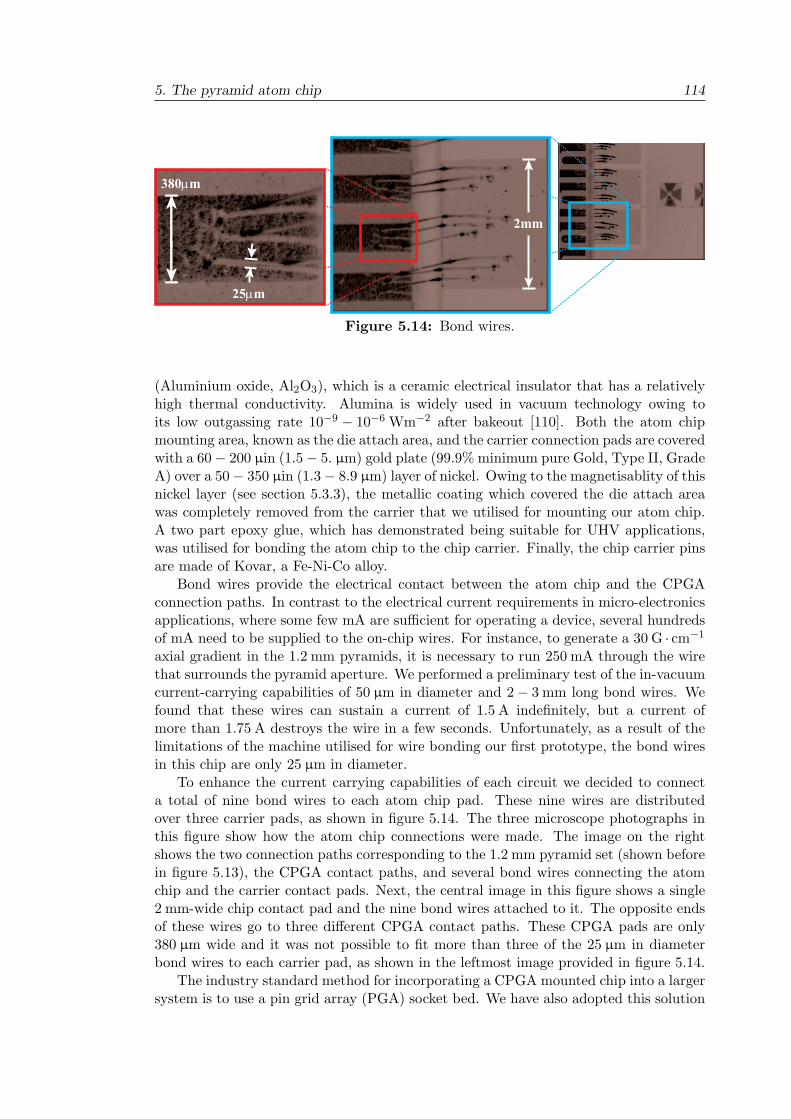
5. The pyramid atom chip 114
2mm
380µm
25µm
Figure 5.14: Bond wires.
(Aluminium oxide, Al2O3), which is a ceramic electrical insulator that has a relativelyhigh thermal conductivity. Alumina is widely used in vacuum technology owing toits low outgassing rate 10"9 " 10"6 Wm"2 after bakeout [110]. Both the atom chipmounting area, known as the die attach area, and the carrier connection pads are coveredwith a 60" 200 µin (1.5" 5. µm) gold plate (99.9% minimum pure Gold, Type II, GradeA) over a 50" 350 µin (1.3" 8.9 µm) layer of nickel. Owing to the magnetisablity of thisnickel layer (see section 5.3.3), the metallic coating which covered the die attach areawas completely removed from the carrier that we utilised for mounting our atom chip.A two part epoxy glue, which has demonstrated being suitable for UHV applications,was utilised for bonding the atom chip to the chip carrier. Finally, the chip carrier pinsare made of Kovar, a Fe-Ni-Co alloy.
Bond wires provide the electrical contact between the atom chip and the CPGAconnection paths. In contrast to the electrical current requirements in micro-electronicsapplications, where some few mA are su!cient for operating a device, several hundredsof mA need to be supplied to the on-chip wires. For instance, to generate a 30 G · cm"1
axial gradient in the 1.2 mm pyramids, it is necessary to run 250 mA through the wirethat surrounds the pyramid aperture. We performed a preliminary test of the in-vacuumcurrent-carrying capabilities of 50 µm in diameter and 2" 3 mm long bond wires. Wefound that these wires can sustain a current of 1.5 A indefinitely, but a current ofmore than 1.75 A destroys the wire in a few seconds. Unfortunately, as a result of thelimitations of the machine utilised for wire bonding our first prototype, the bond wiresin this chip are only 25 µm in diameter.
To enhance the current carrying capabilities of each circuit we decided to connecta total of nine bond wires to each atom chip pad. These nine wires are distributedover three carrier pads, as shown in figure 5.14. The three microscope photographs inthis figure show how the atom chip connections were made. The image on the rightshows the two connection paths corresponding to the 1.2 mm pyramid set (shown beforein figure 5.13), the CPGA contact paths, and several bond wires connecting the atomchip and the carrier contact pads. Next, the central image in this figure shows a single2 mm-wide chip contact pad and the nine bond wires attached to it. The opposite endsof these wires go to three di"erent CPGA contact paths. These CPGA pads are only380 µm wide and it was not possible to fit more than three of the 25 µm in diameterbond wires to each carrier pad, as shown in the leftmost image provided in figure 5.14.
The industry standard method for incorporating a CPGA mounted chip into a largersystem is to use a pin grid array (PGA) socket bed. We have also adopted this solution
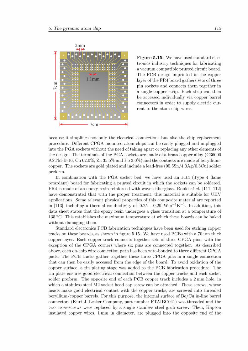
5. The pyramid atom chip 115
7cm
7cm
2mm
1.1mm
Figure 5.15: We have used standard elec-tronics industry techniques for fabricatinga vacuum compatible printed circuit board.The PCB design imprinted in the copperlayer of the FR4 board gathers sets of threepin sockets and connects them together ina single copper strip. Each strip can thenbe accessed individually via copper barrelconnectors in order to supply electric cur-rent to the atom chip wires.
because it simplifies not only the electrical connections but also the chip replacementprocedure. Di"erent CPGA mounted atom chips can be easily plugged and unpluggedinto the PGA sockets without the need of taking apart or replacing any other elements ofthe design. The terminals of the PGA sockets are made of a brass-copper alloy (C36000ASTM-B-16; Cu 62.0%, Zn 35.5% and Pb 3.0%) and the contacts are made of beryllium-copper. The sockets are gold plated and include a lead-free (95.5Sn/4.0Ag/0.5Cu) solderpreform.
In combination with the PGA socket bed, we have used an FR4 (Type 4 flameretardant) board for fabricating a printed circuit in which the sockets can be soldered.FR4 is made of an epoxy resin reinforced with woven fiberglass. Rouki et al. [111, 112]have demonstrated that with the proper treatment, this material is suitable for UHVapplications. Some relevant physical properties of this composite material are reportedin [113], including a thermal conductivity of [0.25" 0.29] Wm"1K"1. In addition, thisdata sheet states that the epoxy resin undergoes a glass transition at a temperature of135 !C. This establishes the maximum temperature at which these boards can be bakedwithout damaging them.
Standard electronics PCB fabrication techniques have been used for etching coppertracks on these boards, as shown in figure 5.15. We have used PCBs with a 70 µm thickcopper layer. Each copper track connects together sets of three CPGA pins, with theexception of the CPGA corners where six pins are connected together. As describedabove, each on-chip wire connection path has been wire-bonded to three di"erent CPGApads. The PCB tracks gather together these three CPGA pins in a single connectionthat can then be easily accessed from the edge of the board. To avoid oxidation of thecopper surface, a tin plating stage was added to the PCB fabrication procedure. Thetin plate ensures good electrical connection between the copper tracks and each socketsolder preform. The opposite end of each PCB copper track includes a 2 mm hole, inwhich a stainless steel M2 socket head cap screw can be attached. These screws, whoseheads make good electrical contact with the copper tracks, are screwed into threadedberyllium/copper barrels. For this purpose, the internal surface of Be/Cu in-line barrelconnectors (Kurt J. Lesker Company, part number FTAIBC041) was threaded and thetwo cross-screws were replaced by a single stainless steel grub screw. Then, Kaptoninsulated copper wires, 1 mm in diameter, are plugged into the opposite end of the
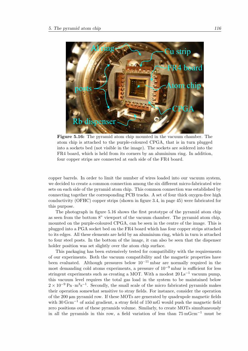
5. The pyramid atom chip 116
Cu stripAl ring
FR4 board
Atom chipposts
Rb dispenserCPGA
Figure 5.16: The pyramid atom chip mounted in the vacuum chamber. Theatom chip is attached to the purple-coloured CPGA, that is in turn pluggedinto a sockets bed (not visible in the image). The sockets are soldered into theFR4 board, which is held from its corners by an aluminium ring. In addition,four copper strips are connected at each side of the FR4 board.
copper barrels. In order to limit the number of wires loaded into our vacuum system,we decided to create a common connection among the six di"erent micro-fabricated wiresets on each side of the pyramid atom chip. This common connection was established byconnecting together the corresponding PCB tracks. A set of four thick oxygen-free highconductivity (OFHC) copper strips (shown in figure 3.4, in page 45) were fabricated forthis purpose.
The photograph in figure 5.16 shows the first prototype of the pyramid atom chipas seen from the bottom 8” viewport of the vacuum chamber. The pyramid atom chip,mounted on the purple-coloured CPGA, can be seen in the centre of the image. This isplugged into a PGA socket bed on the FR4 board which has four copper strips attachedto its edges. All these elements are held by an aluminium ring, which in turn is attachedto four steel posts. In the bottom of the image, it can also be seen that the dispenserholder position was set slightly over the atom chip surface.
This packaging has been extensively tested for compatibility with the requirementsof our experiments. Both the vacuum compatibility and the magnetic properties havebeen evaluated. Although pressures below 10"11 mbar are normally required in themost demanding cold atoms experiments, a pressure of 10"9 mbar is su!cient for lessstringent experiments such as creating a MOT. With a modest 20 Ls"1 vacuum pump,this vacuum level requires the total gas load in the system to be maintained below2# 10"9 Pa ·m3s"1. Secondly, the small scale of the micro fabricated pyramids makestheir operation somewhat sensitive to stray fields. For instance, consider the operationof the 200 µm pyramid row. If these MOTs are generated by quadrupole magnetic fieldswith 30 Gcm"1 of axial gradient, a stray field of 150 mG would push the magnetic fieldzero positions out of these pyramids volume. Similarly, to create MOTs simultaneouslyin all the pyramids in this row, a field variation of less than 75 mGcm"1 must be
5. The pyramid atom chip 117
guaranteed across the atom chip surface.
5.3.2 Vacuum tests of chip packaging resources
The bottom end of a CF full nipple (Kurt J. Lesker Company, FN-0600) was connectedto a turbomolecular pump (TurboVac 150). The nipple top end was sealed with a 6”to 2 3/4” CF reducer flange (Kurt J. Lesker Company, RF600X275). A 2 3/4” CF tee(Kurt J. Lesker Company, T-0275) connected to the reducer was used for connectinga pressure gauge (Pfei"er Vacuum, Compact Full Range BA Gauge, PBR 260) to thechamber. The measurement range of this gauge spans from 5# 10"10 to 103 mbar.
In order to prepare this chamber for testing the atom chip packaging resources, itwas pumped down while still empty. Before baking and after 12 hours of pumping time,a pressure of 10"7 mbar was reached. Next, a single heater tape wound around the top6” blank flange was used for maintaining this section of the chamber at 100 !C. After 24hours of baking at this temperature and allowing the flange to cool back down, a finalpressure of 2# 10"8 mbar was obtained. If the nominal pumping speed of the turbo! 100 Ls"1 is put together with this pressure, a ! 10"6 Ws"1 outgassing rate is deducedfor the stainless steel chamber after baking. This value is still high compared with therange reported by Delchar after bake-out ([10"11 " 10"8] Wm"2) [110]. However, it hasto be taken into account that only a small portion of the chamber was kept at 100 !Cduring the bake-out period. In fact, to avoid any damage to the gauge, the 2 3/4” teeport connecting to the gauge had to be kept at no more than 50 !C.
To continue, we loaded into the test chamber a 7# 7 cm2 FR4 board patterned asshown in figure 5.15. Two aluminium posts attached to the reducer flange were used forholding this PCB into the vacuum test chamber. After 2.5 hours of pumping down, apressure of 2# 10"6 mbar was reached. Next, two heater tapes were wound around boththe reducer flange and the top section of the nipple. The nipple top section and reducerflange were then covered with aluminium foil and the test chamber was heated until thetemperature of the reducer flange reached 130 !C. After baking at this temperature forthree and a half days, the minimum pressure attained while baking was 2# 10"7 mbar.Next, the system was allowed to cool down to room temperature and a final pressure of10"8 mbar was recorded. We were also interested in evaluating the amount of humidityabsorbed by the FR4 board when exposed to air after being baked out in vacuum.Therefore, we continued our tests by venting the system to nitrogen and then to air.The chamber was left open to air for one hour and afterwards the system was pumpeddown again. The 10"8 mbar pressure found before was recovered after just one day ofpumping without needing to bake the test chamber again.
Finally, the PCB was replaced by a new FR4 board which included PGA socketsand a CPGA. A pressure of 1.5 # 10"6 mbar was reached after pumping for two dayswithout baking the system. Next, the chamber was baked at 130 !C for two daysand a minimum pressure of 8.6# 10"7 mbar was obtained while baking. When thesystem was allowed to go back down to room temperature, we measured a pressure of3# 10"8 mbar. The chamber was then vented to air for a couple of hours and pumpedback down again. A pressure of 2 # 10"8 mbar was recovered in 4 hours. Baking thesystem by heating the 6” nipple at 150 !C for up to 5 days resulted in a final pressure,after cooling down, of 3# 10"9 mbar. The chamber was opened, closed and pumpeddown once more. A pressure of 10"8 mbar was recovered in one day, but it finally camedown to 3# 10"9 mbar in a week.
Thus, the vacuum compatibility of each element of the chip packaging arrangement
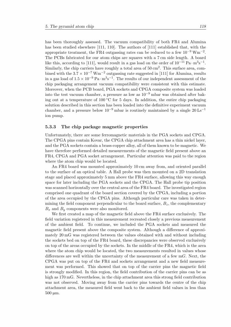
5. The pyramid atom chip 118
has been thoroughly assessed. The vacuum compatibility of both FR4 and Aluminahas been studied elsewhere [111, 110]. The authors of [111] established that, with theappropriate treatment, the FR4 outgassing rates can be reduced to a few 10"9 Wm"2.The PCBs fabricated for our atom chips are squares with a 7 cm side length. A boardlike this, according to [111], would result in a gas load on the order of 10"11 Pa ·m3s"1.Similarly, the chip carriers have roughly a total area of 50 cm2. This surface area, com-bined with the 3.7# 10"7 Wm"2 outgassing rate suggested in [111] for Alumina, resultsin a gas load of 1.5# 10"9 Pa ·m3s"1. The results of our independent assessment of thechip packaging arrangement vacuum compatibility were consistent with this estimate.Moreover, when the PCB board, PGA sockets and CPGA composite system was loadedinto the test vacuum chamber, a pressure as low as 10"9 mbar was obtained after bak-ing out at a temperature of 100 !C for 5 days. In addition, the entire chip packagingsolution described in this section has been loaded into the definitive experiment vacuumchamber, and a pressure below 10"9 mbar is routinely maintained by a single 20 Ls"1
ion pump.
5.3.3 The chip package magnetic properties
Unfortunately, there are some ferromagnetic materials in the PGA sockets and CPGA.The CPGA pins contain Kovar, the CPGA chip attachment area has a thin nickel layer,and the PGA sockets contain a brass-copper alloy, all of them known to be magnetic. Wehave therefore performed detailed measurements of the magnetic field present above anFR4, CPGA and PGA socket arrangement. Particular attention was paid to the regionwhere the atom chip would be located.
An FR4 board was mounted approximately 10 cm away from, and oriented parallelto the surface of an optical table. A Hall probe was then mounted on a 2D translationstage and placed approximately 5 mm above the FR4 surface, allowing this way enoughspace for later including the PGA sockets and the CPGA. The Hall probe tip positionwas scanned horizontally over the central area of the FR4 board. The investigated regioncomprised one quadrant of the board section covered by the CPGA, including a portionof the area occupied by the CPGA pins. Although particular care was taken in deter-mining the field component perpendicular to the board surface, Bz, the complementaryBx and By components were also monitored.
We first created a map of the magnetic field above the FR4 surface exclusively. Thefield variation registered in this measurement recreated closely a previous measurementof the ambient field. To continue, we included the PGA sockets and measured themagnetic field present above the composite system. Although a di"erence of approxi-mately 20 mG was registered between the values obtained with and without includingthe sockets bed on top of the FR4 board, these discrepancies were observed exclusivelyon top of the areas occupied by the sockets. In the middle of the FR4, which is the areawhere the atom chip would be located, the two measurements resulted in values whosedi"erences are well within the uncertainty of the measurement of a few mG. Next, theCPGA was put on top of the FR4 and sockets arrangement and a new field measure-ment was performed. This showed that on top of the carrier pins the magnetic fieldis strongly modified. In this region, the field contribution of the carrier pins can be ashigh as 170 mG. Nevertheless, in the chip attachment area this strong field contributionwas not observed. Moving away from the carrier pins towards the centre of the chipattachment area, the measured field went back to the ambient field values in less than500 µm.
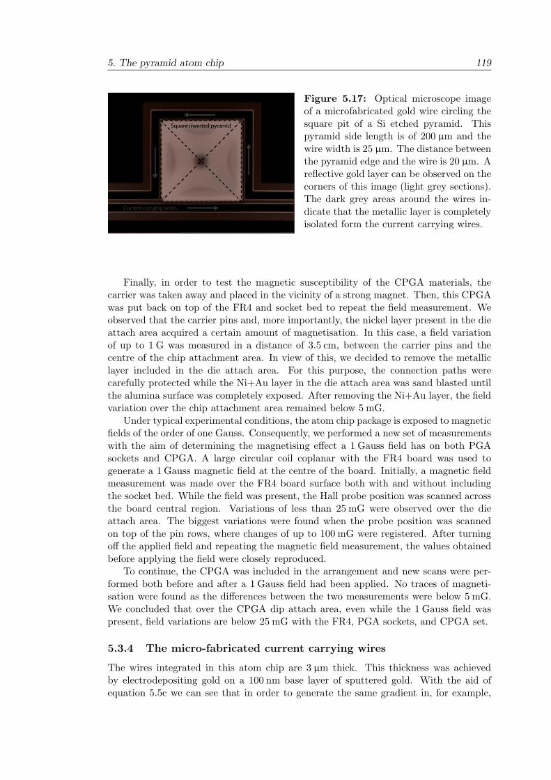
5. The pyramid atom chip 119
Figure 5.17: Optical microscope imageof a microfabricated gold wire circling thesquare pit of a Si etched pyramid. Thispyramid side length is of 200 µm and thewire width is 25 µm. The distance betweenthe pyramid edge and the wire is 20 µm. Areflective gold layer can be observed on thecorners of this image (light grey sections).The dark grey areas around the wires in-dicate that the metallic layer is completelyisolated form the current carrying wires.
Finally, in order to test the magnetic susceptibility of the CPGA materials, thecarrier was taken away and placed in the vicinity of a strong magnet. Then, this CPGAwas put back on top of the FR4 and socket bed to repeat the field measurement. Weobserved that the carrier pins and, more importantly, the nickel layer present in the dieattach area acquired a certain amount of magnetisation. In this case, a field variationof up to 1 G was measured in a distance of 3.5 cm, between the carrier pins and thecentre of the chip attachment area. In view of this, we decided to remove the metalliclayer included in the die attach area. For this purpose, the connection paths werecarefully protected while the Ni+Au layer in the die attach area was sand blasted untilthe alumina surface was completely exposed. After removing the Ni+Au layer, the fieldvariation over the chip attachment area remained below 5 mG.
Under typical experimental conditions, the atom chip package is exposed to magneticfields of the order of one Gauss. Consequently, we performed a new set of measurementswith the aim of determining the magnetising e"ect a 1 Gauss field has on both PGAsockets and CPGA. A large circular coil coplanar with the FR4 board was used togenerate a 1 Gauss magnetic field at the centre of the board. Initially, a magnetic fieldmeasurement was made over the FR4 board surface both with and without includingthe socket bed. While the field was present, the Hall probe position was scanned acrossthe board central region. Variations of less than 25 mG were observed over the dieattach area. The biggest variations were found when the probe position was scannedon top of the pin rows, where changes of up to 100 mG were registered. After turningo" the applied field and repeating the magnetic field measurement, the values obtainedbefore applying the field were closely reproduced.
To continue, the CPGA was included in the arrangement and new scans were per-formed both before and after a 1 Gauss field had been applied. No traces of magneti-sation were found as the di"erences between the two measurements were below 5 mG.We concluded that over the CPGA dip attach area, even while the 1 Gauss field waspresent, field variations are below 25 mG with the FR4, PGA sockets, and CPGA set.
5.3.4 The micro-fabricated current carrying wires
The wires integrated in this atom chip are 3 µm thick. This thickness was achievedby electrodepositing gold on a 100 nm base layer of sputtered gold. With the aid ofequation 5.5c we can see that in order to generate the same gradient in, for example,
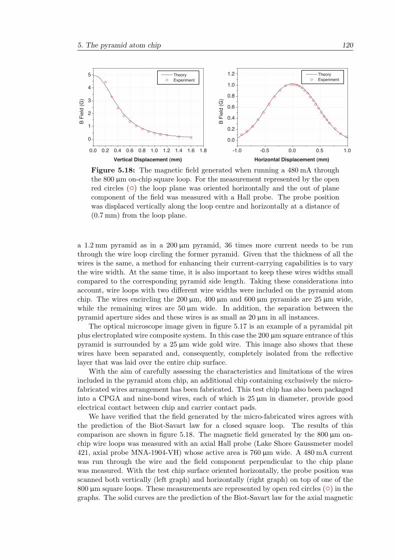
5. The pyramid atom chip 120
0.0 0.2 0.4 0.6 0.8 1.0 1.2 1.4 1.6 1.8
0
1
2
3
4
5
-1.0 -0.5 0.0 0.5 1.0
0.0
0.2
0.4
0.6
0.8
1.0
1.2 Theory Experiment
B Fi
eld
(G)
Vertical Displacement (mm)
Theory Experiment
B Fi
eld
(G)
Horizontal Displacement (mm)
Figure 5.18: The magnetic field generated when running a 480 mA throughthe 800 µm on-chip square loop. For the measurement represented by the openred circles (0) the loop plane was oriented horizontally and the out of planecomponent of the field was measured with a Hall probe. The probe positionwas displaced vertically along the loop centre and horizontally at a distance of(0.7 mm) from the loop plane.
a 1.2 mm pyramid as in a 200 µm pyramid, 36 times more current needs to be runthrough the wire loop circling the former pyramid. Given that the thickness of all thewires is the same, a method for enhancing their current-carrying capabilities is to varythe wire width. At the same time, it is also important to keep these wires widths smallcompared to the corresponding pyramid side length. Taking these considerations intoaccount, wire loops with two di"erent wire widths were included on the pyramid atomchip. The wires encircling the 200 µm, 400 µm and 600 µm pyramids are 25 µm wide,while the remaining wires are 50 µm wide. In addition, the separation between thepyramid aperture sides and these wires is as small as 20 µm in all instances.
The optical microscope image given in figure 5.17 is an example of a pyramidal pitplus electroplated wire composite system. In this case the 200 µm square entrance of thispyramid is surrounded by a 25 µm wide gold wire. This image also shows that thesewires have been separated and, consequently, completely isolated from the reflectivelayer that was laid over the entire chip surface.
With the aim of carefully assessing the characteristics and limitations of the wiresincluded in the pyramid atom chip, an additional chip containing exclusively the micro-fabricated wires arrangement has been fabricated. This test chip has also been packagedinto a CPGA and nine-bond wires, each of which is 25 µm in diameter, provide goodelectrical contact between chip and carrier contact pads.
We have verified that the field generated by the micro-fabricated wires agrees withthe prediction of the Biot-Savart law for a closed square loop. The results of thiscomparison are shown in figure 5.18. The magnetic field generated by the 800 µm on-chip wire loops was measured with an axial Hall probe (Lake Shore Gaussmeter model421, axial probe MNA-1904-VH) whose active area is 760 µm wide. A 480 mA currentwas run through the wire and the field component perpendicular to the chip planewas measured. With the test chip surface oriented horizontally, the probe position wasscanned both vertically (left graph) and horizontally (right graph) on top of one of the800 µm square loops. These measurements are represented by open red circles (0) in thegraphs. The solid curves are the prediction of the Biot-Savart law for the axial magnetic
5. The pyramid atom chip 121
Figure 5.19: The micro-facricated wires blow up just as if they were fuses.The 50 µm-wide wire blows with a current of 1.8 A and the 25 µm-wide wirecan not withstand more than 0.8 A. These optical microscope images of thefailure points in each case clearly indicate that the 50 µm-wide wire meltedbefore a short circuit destroyed it; the 25 µm-wide failure on the other handwas probably originated from a small defect in the electroplated wire.
field component generated by a closed 50 µm wide wire loop, centred on a 895 µm squareand running a current of 480 mA. There is an excellent agreement between the theoryand experiment.
We have also determined the maximum current that can be run through the atomchip micro-fabricated wires, and how long currents can be sustained without damagingthe chip wires. For this purpose, we performed a series of tests under moderate vacuum(! 10"5 mbar) conditions. The temperature variation at three di"erent points of thechip packaging arrangement was closely monitored. Thermocouples located on top ofthe test chip surface, next to the CPGA pins and on the edge of the FR4 board wereused for monitoring the temperature. In addition, the change in the resistance on thecurrent carrying wires was also monitored.
The maximum current that can be applied through the chip wires was determinedby increasing the current in small ! 10 mA steps. After each increment, we waited forthe temperature of the wire to stabilise before going to the next current. We repeatedthis procedure in a 50 µm-wide wire and in a 25 µm-wide wire. The former blows atapproximately 1.8 A and the latter at 0.8 A. The images shown in figure 5.19 are opticalmicroscope images of the points were the failure of the wires took place. The cause ofthe failure in the 25 µm-wide wire could have been a defect of the wire, while in the caseof the 50 µm-wide wire seems clear that the heat dissipated was enough for melting thegold and producing a short circuit between the two wires. Note the di"erences in thewire surface roughness between the regions where the wire exploded and where it stillshows the result of the electroplating process.
Figure 5.20 shows the time during which a given current can be applied through a25 µm-wide wire (!) and through a 50 µm-wide wire (•) before its temperature reaches120 !C, which is the safe operation limit determined by the chip packaging materials.The epoxy glue used for bonding the pyramid atom chip to the CPGA su"ers a glasstransition at a temperature of approximately 120 !C. Similarly, the FR4 data sheet
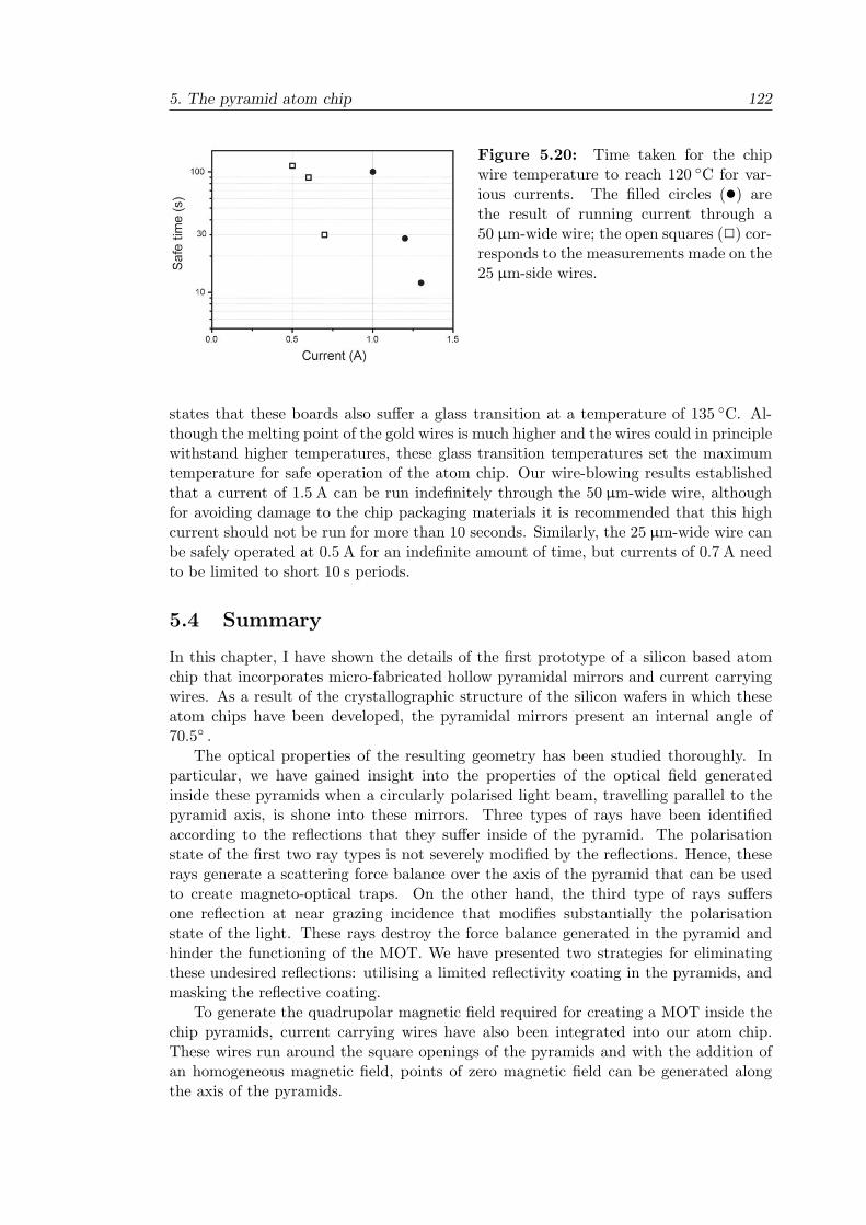
5. The pyramid atom chip 122
Figure 5.20: Time taken for the chipwire temperature to reach 120 !C for var-ious currents. The filled circles (•) arethe result of running current through a50 µm-wide wire; the open squares (!) cor-responds to the measurements made on the25 µm-side wires.
states that these boards also su"er a glass transition at a temperature of 135 !C. Al-though the melting point of the gold wires is much higher and the wires could in principlewithstand higher temperatures, these glass transition temperatures set the maximumtemperature for safe operation of the atom chip. Our wire-blowing results establishedthat a current of 1.5 A can be run indefinitely through the 50 µm-wide wire, althoughfor avoiding damage to the chip packaging materials it is recommended that this highcurrent should not be run for more than 10 seconds. Similarly, the 25 µm-wide wire canbe safely operated at 0.5 A for an indefinite amount of time, but currents of 0.7 A needto be limited to short 10 s periods.
5.4 Summary
In this chapter, I have shown the details of the first prototype of a silicon based atomchip that incorporates micro-fabricated hollow pyramidal mirrors and current carryingwires. As a result of the crystallographic structure of the silicon wafers in which theseatom chips have been developed, the pyramidal mirrors present an internal angle of70.5! .
The optical properties of the resulting geometry has been studied thoroughly. Inparticular, we have gained insight into the properties of the optical field generatedinside these pyramids when a circularly polarised light beam, travelling parallel to thepyramid axis, is shone into these mirrors. Three types of rays have been identifiedaccording to the reflections that they su"er inside of the pyramid. The polarisationstate of the first two ray types is not severely modified by the reflections. Hence, theserays generate a scattering force balance over the axis of the pyramid that can be usedto create magneto-optical traps. On the other hand, the third type of rays su"ersone reflection at near grazing incidence that modifies substantially the polarisationstate of the light. These rays destroy the force balance generated in the pyramid andhinder the functioning of the MOT. We have presented two strategies for eliminatingthese undesired reflections: utilising a limited reflectivity coating in the pyramids, andmasking the reflective coating.
To generate the quadrupolar magnetic field required for creating a MOT inside thechip pyramids, current carrying wires have also been integrated into our atom chip.These wires run around the square openings of the pyramids and with the addition ofan homogeneous magnetic field, points of zero magnetic field can be generated alongthe axis of the pyramids.

5. The pyramid atom chip 123
Finally, micro-electronics industry standard micro-chip packaging tools and tech-niques have been utilised for loading and holding the pyramids and wires atom chipinto the vacuum chamber, as well as for supplying current to the on-chip wires. Ex-tensive vacuum and magnetisability tests were performed to ensure the compatibilityof these elements with the requirements of cold atom experiments. As well, the flow ofthe heat generated by the chip wires through the experimental apparatus was carefullystudied with the aim of establishing the safe operation limits of the device.
124
Chapter 6
Co/Pt magneto-optic thin films
In this chapter I describe the properties of a permanently magnetised medium thatis suitable for applications in atom chips. The magneto-optic thin films composedby alternating layers of cobalt and platinum (Co/Pt MO films) can be engineered toproduce a medium that retains a large amount of magnetisation. Hence, the Co/Ptmagneto-optic thin films are strong enough to make magnetostatic atom traps andcould replace the current carrying wires in future integrated pyramid MOT chips.
To begin with, I provide a brief introduction to the physics of magnetic thin filmsand the required fabrication techniques. These concepts are necessary for evaluatingthe potential uses of these films. Then, the properties of the Co/Pt multilayer structurewill be outlined to show why these films are particularly suitable for creating cold atommicro-traps. To continue, I describe the thermomagnetic recording technique that wehave used for creating microscopic magnetic patterns on the surface of Co/Pt MO thinfilms. Finally, the results obtained by means of this technique are shown together withnumerical estimates of the corresponding magnetic fields.
6.1 Magneto-optic multi-layer thin films
Magneto-optic (MO) films have been commercially used to produce high density record-ing media such as the minidisk. According to [114], the high anisotropy of these filmsallows thermally stable magnetic grains with sizes below 10 nm. Among other interestingproperties, these magnetic films are characterised by a large out-of-plane magnetisation,an exceptionally strong remanent field, a high room-temperature coercivity and a largeKerr angle at short wavelengths. These properties make MO films technology speciallysuitable for applications in atom optics.
6.1.1 Preparation of multi-layer films
A magneto optic thin film is composed by a series of material layers. First of all, asubstrate provides a surface that can be assumed as perfectly smooth. Then, a seedlayer or insulation layer provides an initial texture and grain growth templates. This
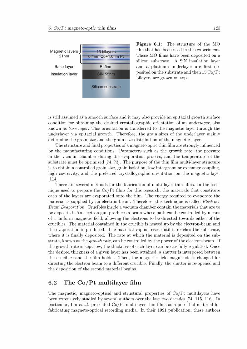
6. Co/Pt magneto-optic thin films 125
Silicon substrate
SiN 55nm
Pt 5nm
15 bilayers0.4nm Co+1.0nm Pt
Insulation layer
Base layer
Magnetic layers21nm
Figure 6.1: The structure of the MOfilm that has been used in this experiment.These MO films have been deposited on asilicon substrate. A SiN insulation layerand a platinum underlayer are first de-posited on the substrate and then 15 Co/Ptbilayers are grown on top.
is still assumed as a smooth surface and it may also provide an epitaxial growth surfacecondition for obtaining the desired crystallographic orientation of an underlayer, alsoknown as base layer. This orientation is transferred to the magnetic layer through theunderlayer via epitaxial growth. Therefore, the grain sizes of the underlayer mainlydetermine the grain size and the grain size distribution of the magnetic layer.
The structure and final properties of a magneto optic thin film are strongly influencedby the manufacturing conditions. Parameters such as the growth rate, the pressurein the vacuum chamber during the evaporation process, and the temperature of thesubstrate must be optimized [74, 73]. The purpose of the thin film multi-layer structureis to obtain a controlled grain size, grain isolation, low intergranular exchange coupling,high coercivity, and the preferred crystallographic orientation on the magnetic layer[114].
There are several methods for the fabrication of multi-layer thin films. In the tech-nique used to prepare the Co/Pt films for this research, the materials that constituteeach of the layers are evaporated onto the film. The energy required to evaporate thematerial is supplied by an electron-beam. Therefore, this technique is called Electron-Beam Evaporation. Crucibles inside a vacuum chamber contain the materials that are tobe deposited. An electron gun produces a beam whose path can be controlled by meansof a uniform magnetic field, allowing the electrons to be directed towards either of thecrucibles. The material contained in the crucible is heated up by the electron-beam andthe evaporation is produced. The material vapour rises until it reaches the substrate,where it is finally deposited. The rate at which the material is deposited on the sub-strate, known as the growth rate, can be controlled by the power of the electron-beam. Ifthe growth rate is kept low, the thickness of each layer can be carefully regulated. Oncethe desired thickness of a given layer has been attained, a shutter is interposed betweenthe crucibles and the film holder. Then, the magnetic field magnitude is changed fordirecting the electron beam to a di"erent crucible. Finally, the shutter is re-opened andthe deposition of the second material begins.
6.2 The Co/Pt multilayer film
The magnetic, magneto-optical and structural properties of Co/Pt multilayers havebeen extensively studied by several authors over the last two decades [74, 115, 116]. Inparticular, Lin et al. presented Co/Pt multilayer thin films as a potential material forfabricating magneto-optical recording media. In their 1991 publication, these authors
6. Co/Pt magneto-optic thin films 126
explain that the largest perpendicular anisotropy occurs for Co layer thickness of 1-2monolayers and that perfectly square hysteresis loops are obtained for multilayers ofCo3 A/Pt10 A with thickness up to about 10 periods. Similarly, the domain structureand magnetisation reversal processes in these films have been extensively studied [117,118, 119, 120].
The fabrication of the Co/Pt multilayer thin films in this thesis was optimised for cre-ating microscopic atom traps and guides. We wanted a large perpendicular anisotropyto allow the creation of well defined patterns with extremely thin boundaries betweenregions magnetised in opposite directions. We also wanted strong saturation magnetisa-tion and coercivity. These allow tight atom traps to be generated at very short distancesfrom these films.
As shown in Fig. 6.1, the magneto-optical films were deposited on silicon substrateswith a 550 A silicon-nitride (SiN) insulation layer. The insulation layer was held at200 !C while a thick platinum base layer of 50 A established a good 111 texture. Later,15 bi-layers of alternating Co (4 A) and Pt (10 A) were prepared by electron-beam evap-oration onto the 111 base layer. In order to ensure good control of the layer thickness,the evaporation rate was kept as low as 0.1 As"1.
6.2.1 Crystal structure
The magnetic properties of the Co/Pt thin films and particularly its magnetic anisotropydepend strongly on the crystallographic orientation of the layers. In a ferromagneticcrystal, the magnetisation is directed along certain definite crystallographic axes, calleddirections of easy magnetisation or just easy directions. For example, while bulk plat-inum establishes a cubic close-packed (ccp) crystal structure, the crystal structureadopted by bulk cobalt is hexagonal closed-packed (hcp). The hcp structure of bulkcobalt has an easy direction along its hexagonal axis.
In our case, the platinum underlayer is used to provide epitaxial growth conditionsfor face-centered tetragonal (fct) CoPt grains. These grains grow with their magneticeasy axis perpendicular to the film plane. The cobalt layers in our multi-layer filmsare extremely thin and are sandwiched between layers of platinum with well established111 texture. The growth conditions should assure that the good 111 texture establishedon the platinum base layer is transferred by epitaxial growth to the CoPt layers. InCoPt alloys, the ordered face-centered tetragonal structure (L10 phase) is adopted inthe composition range that goes from 40 to 60 at. %Co [114]. The crystal structureof this fct phase is shown in figure 6.2. It has a superlattice structure consisting of Coand Pt monoatomic layers stacked alternately along the c-axis, which is the magneticeasy axis. This ordered phase can be obtained by deposition of the films on a heatedsubstrate [114].
6.2.2 Magnetic and optical properties
The ferromagnetic component of Co/Pt MO films exhibits a spontaneous magnetisa-tion. This suggests that electron spins and magnetic moments are arranged in a regularmanner within the multi-layer structure of the film. Microscopically, even in the unmag-netised state, the magnetisation of a film is not uniform. The entire magnetic layer isdivided into magnetic domains, each with its own magnetisation state. These domainsare tiny volumes uniformly magnetised with a spontaneous magnetisation Ms in an easydirection, which in our case is perpendicular to the film surface. The transition volumes
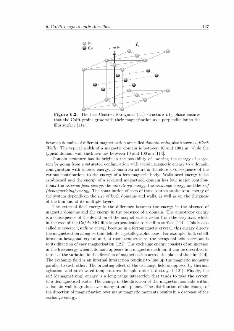
6. Co/Pt magneto-optic thin films 127
c-axisPtCo
Figure 6.2: The face-Centred tetragonal (fct) structure L10 phase ensuresthat the CoPt grains grow with their magnetisation axis perpendicular to thefilm surface [114].
between domains of di"erent magnetisation are called domain walls, also known as BlochWalls. The typical width of a magnetic domain is between 10 and 100 µm, while thetypical domain wall thickness lies between 10 and 100 nm [114].
Domain structure has its origin in the possibility of lowering the energy of a sys-tem by going from a saturated configuration with certain magnetic energy to a domainconfiguration with a lower energy. Domain structure is therefore a consequence of thevarious contributions to the energy of a ferromagnetic body. Walls need energy to beestablished and the energy of a reversed magnetised domain has four major contribu-tions: the external field energy, the anisotropy energy, the exchange energy and the self(demagnetising) energy. The contribution of each of these sources to the total energy ofthe system depends on the size of both domains and walls, as well as on the thicknessof the film and of its multiple layers.
The external field energy is the di"erence between the energy in the absence ofmagnetic domains and the energy in the presence of a domain. The anisotropy energyis a consequence of the deviation of the magnetisation vector from the easy axis, whichin the case of the Co/Pt MO film is perpendicular to the film surface [114]. This is alsocalled magnetocrystalline energy because in a ferromagnetic crystal, this energy directsthe magnetisation along certain definite crystallographic axes. For example, bulk cobaltforms an hexagonal crystal and, at room temperature, the hexagonal axis correspondsto its direction of easy magnetisation [121]. The exchange energy consists of an increasein the free energy when a domain appears in a magnetic medium; it can be described interms of the variation in the direction of magnetisation across the plane of the film [114].The exchange field is an internal interaction tending to line up the magnetic momentsparallel to each other. The orienting e"ect of the exchange field is opposed by thermalagitation, and at elevated temperatures the spin order is destroyed [121]. Finally, theself (demagnetising) energy is a long range interaction that tends to take the systemto a demagnetised state. The change in the direction of the magnetic moments withina domain wall is gradual over many atomic planes. The distribution of the change ofthe direction of magnetisation over many magnetic moments results in a decrease of theexchange energy.
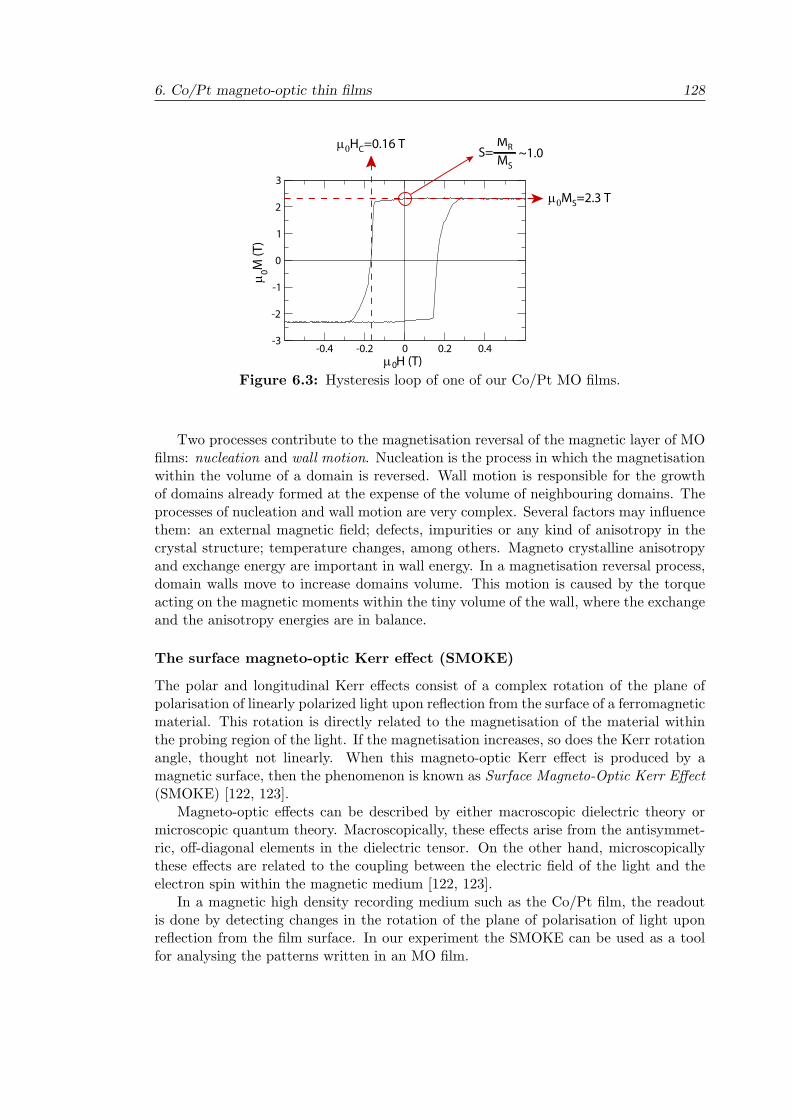
6. Co/Pt magneto-optic thin films 128
-0.4 -0.2 0 0.2 0.4µ0H (T)
-3
-2
-1
0
1
2
3
µ 0M (T
)
µ0MS=2.3 T
µ0HC=0.16 TMS
MRS= ~1.0
Figure 6.3: Hysteresis loop of one of our Co/Pt MO films.
Two processes contribute to the magnetisation reversal of the magnetic layer of MOfilms: nucleation and wall motion. Nucleation is the process in which the magnetisationwithin the volume of a domain is reversed. Wall motion is responsible for the growthof domains already formed at the expense of the volume of neighbouring domains. Theprocesses of nucleation and wall motion are very complex. Several factors may influencethem: an external magnetic field; defects, impurities or any kind of anisotropy in thecrystal structure; temperature changes, among others. Magneto crystalline anisotropyand exchange energy are important in wall energy. In a magnetisation reversal process,domain walls move to increase domains volume. This motion is caused by the torqueacting on the magnetic moments within the tiny volume of the wall, where the exchangeand the anisotropy energies are in balance.
The surface magneto-optic Kerr e!ect (SMOKE)
The polar and longitudinal Kerr e"ects consist of a complex rotation of the plane ofpolarisation of linearly polarized light upon reflection from the surface of a ferromagneticmaterial. This rotation is directly related to the magnetisation of the material withinthe probing region of the light. If the magnetisation increases, so does the Kerr rotationangle, thought not linearly. When this magneto-optic Kerr e"ect is produced by amagnetic surface, then the phenomenon is known as Surface Magneto-Optic Kerr E!ect(SMOKE) [122, 123].
Magneto-optic e"ects can be described by either macroscopic dielectric theory ormicroscopic quantum theory. Macroscopically, these e"ects arise from the antisymmet-ric, o"-diagonal elements in the dielectric tensor. On the other hand, microscopicallythese e"ects are related to the coupling between the electric field of the light and theelectron spin within the magnetic medium [122, 123].
In a magnetic high density recording medium such as the Co/Pt film, the readoutis done by detecting changes in the rotation of the plane of polarisation of light uponreflection from the film surface. In our experiment the SMOKE can be used as a toolfor analysing the patterns written in an MO film.
6. Co/Pt magneto-optic thin films 129
6.2.3 Characterization of MO films
The magnetic properties of the films used in this experiment were determined using analternating gradient force magnetometer (AGFM) [118]. The sensitivity of this deviceis on the order of 10"8 emu = 10"13 A ·m2. In the AGFM, the sample to be analysedis initially magnetised by a field produced by an electromagnet. At the same time, thesample is subject to a small alternating field gradient on the order of a few Oe/mmto a few tens of Oe/mm. This alternating gradient field exerts a force Fx = µdB
dx onthe sample, which rests on one end of an extension cantilever. The opposite end of thiscantilever is held by a piezo-electric biomorph unit, which senses the force exerted on thesample and converts it into an electric signal. The proportionality between the force andthe field gradient, which is given by the magnetic moment µ of the sample, is determinedby this measurement. The magnetisation is in turn defined as the quantity of magneticmoment per unit volume. Consequently, the AGFM allows us to determine a directrelation between the electric signal produced by the piezo unit and the magnetisationof the sample [114].
A set of key properties of a magnetic sample can be determined by analysing thecurve obtained for the magnetisation of the sample versus the applied field, namelyhysteresis loop. Figure 6.3 shows an example of the hysteresis loop for one of our MOfilms. If the sample is initially demagnetised and a low magnetic field is applied, amagnetisation is induced on the sample by means of a reversible domain wall motion.This means that, if this field is turned o" at this point, the sample will recover itsunmagnetised state. By increasing the applied field above this reversible stage, the wallswill move further away and a state of irreversible magnetisation is reached. This happensbecause the magnetisation rotation has to be done against the anisotropy energy. Then,once the magnetisation has been reversed, the anisotropy energy prevents the magneticmoments from relaxing to its initial direction. A further rise of the magnetic field willeventually make the sample reach its saturation magnetisation MS. At this point, thesample has been fully magnetised in the direction of the field and its magnetisationdoes not grow further on increasing the magnetic field. Moreover, after the saturationhas been reached and the magnetic field has been turned o", the magnetisation of thesample will relax to its remanent magnetisation MR.
The ratio S = MRMS
is known as the squareness of the hysteresis loop and is a measureof the relaxation of the magnetisation that the sample su"ers when the magnetisingfield disappears. If the field is now applied in the opposite direction and graduallyincreased as before, the magnetisation of the sample will eventually be reduced to zeroagain. The value of the applied magnetic field at which the magnetisation is reducedto zero is called the coercivity of the film. From the hysteresis loop shown in figure 6.3,the film coercivity is found to be µ0Hc = 0.16 T, while the saturation magnetisationµ0MS = 2.3 T. This represents a magnetisation ! 30% higher in the Co layers thanthat of bulk Co. This occurs because the cobalt layers polarise the nighboring platinumatoms, which in turn contribute to the magnetisation of the sample. In addition, thesquareness of this hysteresis loop (S + 1) guarantees that the sample remains in ahighly magnetised state (µ0MR + 2.3 T) even after the magnetising external field hasbeen removed.
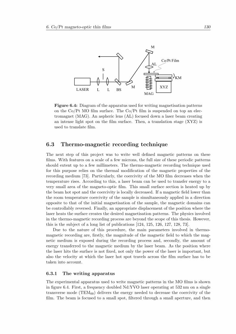
6. Co/Pt magneto-optic thin films 130
MBSL L
S
LASER
M
AL
KM
Co/Pt Film
MAG
XYZ
Figure 6.4: Diagram of the apparatus used for writing magnetisation patternson the Co/Pt MO film surface. The Co/Pt film is suspended on top an elec-tromagnet (MAG). An aspheric lens (AL) focused down a laser beam creatingan intense light spot on the film surface. Then, a translation stage (XYZ) isused to translate film.
6.3 Thermo-magnetic recording technique
The next step of this project was to write well defined magnetic patterns on thesefilms. With features on a scale of a few microns, the full size of these periodic patternsshould extent up to a few millimeters. The thermo-magnetic recording technique usedfor this purpose relies on the thermal modification of the magnetic properties of therecording medium [73]. Particularly, the coercivity of the MO film decreases when thetemperature rises. According to this, a laser beam can be used to transfer energy to avery small area of the magneto-optic film. This small surface section is heated up bythe beam hot spot and the coercivity is locally decreased. If a magnetic field lower thanthe room temperature coercivity of the sample is simultaneously applied in a directionopposite to that of the initial magnetisation of the sample, the magnetic domains canbe controllably reversed. Finally, an appropriate displacement of the position where thelaser heats the surface creates the desired magnetisation patterns. The physics involvedin the thermo-magnetic recording process are beyond the scope of this thesis. However,this is the subject of a long list of publications [124, 125, 126, 127, 128, 73].
Due to the nature of this procedure, the main parameters involved in thermo-magnetic recording are, firstly, the magnitude of the magnetic field to which the mag-netic medium is exposed during the recording process and, secondly, the amount ofenergy transferred to the magnetic medium by the laser beam. As the position wherethe laser hits the surface is not fixed, not only the power of the laser is important, butalso the velocity at which the laser hot spot travels across the film surface has to betaken into account.
6.3.1 The writing apparatus
The experimental apparatus used to write magnetic patterns in the MO films is shownin figure 6.4. First, a frequency doubled Nd:YVO laser operating at 532 nm on a singletransverse mode (TEM00) delivers the energy needed to decrease the coercivity of thefilm. The beam is focused to a small spot, filtered through a small aperture, and then
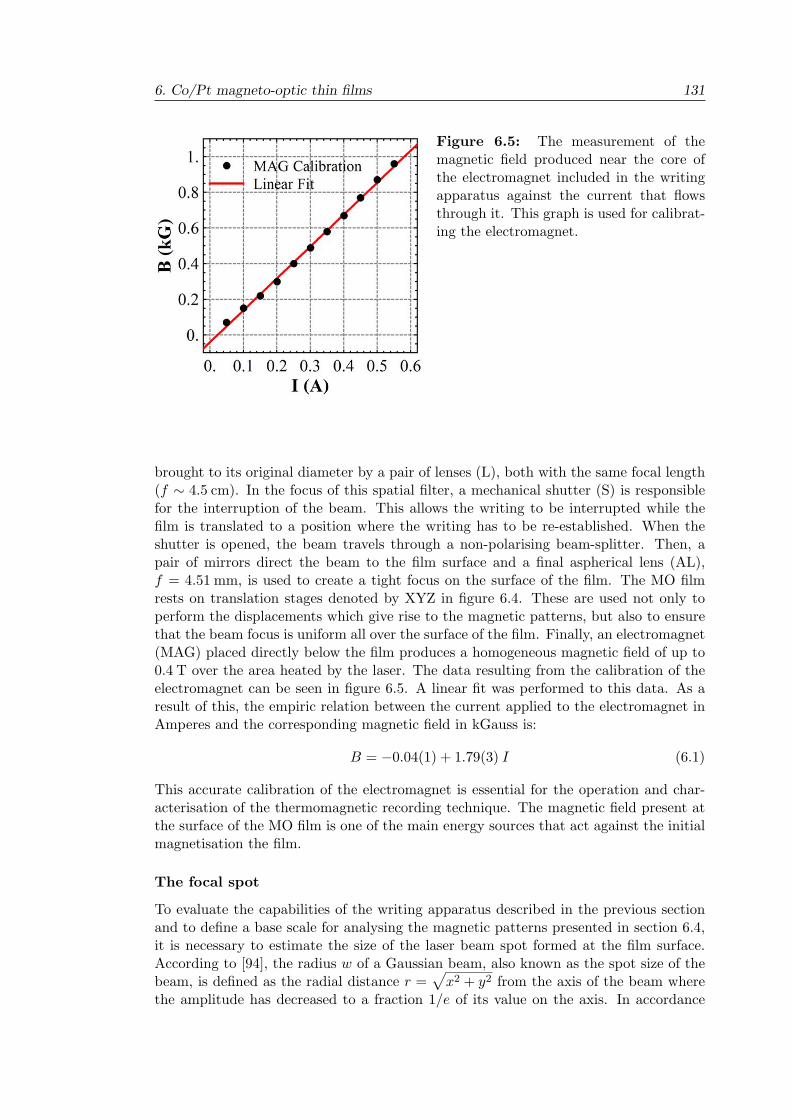
6. Co/Pt magneto-optic thin films 131
Figure 6.5: The measurement of themagnetic field produced near the core ofthe electromagnet included in the writingapparatus against the current that flowsthrough it. This graph is used for calibrat-ing the electromagnet.
brought to its original diameter by a pair of lenses (L), both with the same focal length(f ! 4.5 cm). In the focus of this spatial filter, a mechanical shutter (S) is responsiblefor the interruption of the beam. This allows the writing to be interrupted while thefilm is translated to a position where the writing has to be re-established. When theshutter is opened, the beam travels through a non-polarising beam-splitter. Then, apair of mirrors direct the beam to the film surface and a final aspherical lens (AL),f = 4.51 mm, is used to create a tight focus on the surface of the film. The MO filmrests on translation stages denoted by XYZ in figure 6.4. These are used not only toperform the displacements which give rise to the magnetic patterns, but also to ensurethat the beam focus is uniform all over the surface of the film. Finally, an electromagnet(MAG) placed directly below the film produces a homogeneous magnetic field of up to0.4 T over the area heated by the laser. The data resulting from the calibration of theelectromagnet can be seen in figure 6.5. A linear fit was performed to this data. As aresult of this, the empiric relation between the current applied to the electromagnet inAmperes and the corresponding magnetic field in kGauss is:
B = "0.04(1) + 1.79(3) I (6.1)
This accurate calibration of the electromagnet is essential for the operation and char-acterisation of the thermomagnetic recording technique. The magnetic field present atthe surface of the MO film is one of the main energy sources that act against the initialmagnetisation the film.
The focal spot
To evaluate the capabilities of the writing apparatus described in the previous sectionand to define a base scale for analysing the magnetic patterns presented in section 6.4,it is necessary to estimate the size of the laser beam spot formed at the film surface.According to [94], the radius w of a Gaussian beam, also known as the spot size of thebeam, is defined as the radial distance r =
(x2 + y2 from the axis of the beam where
the amplitude has decreased to a fraction 1/e of its value on the axis. In accordance
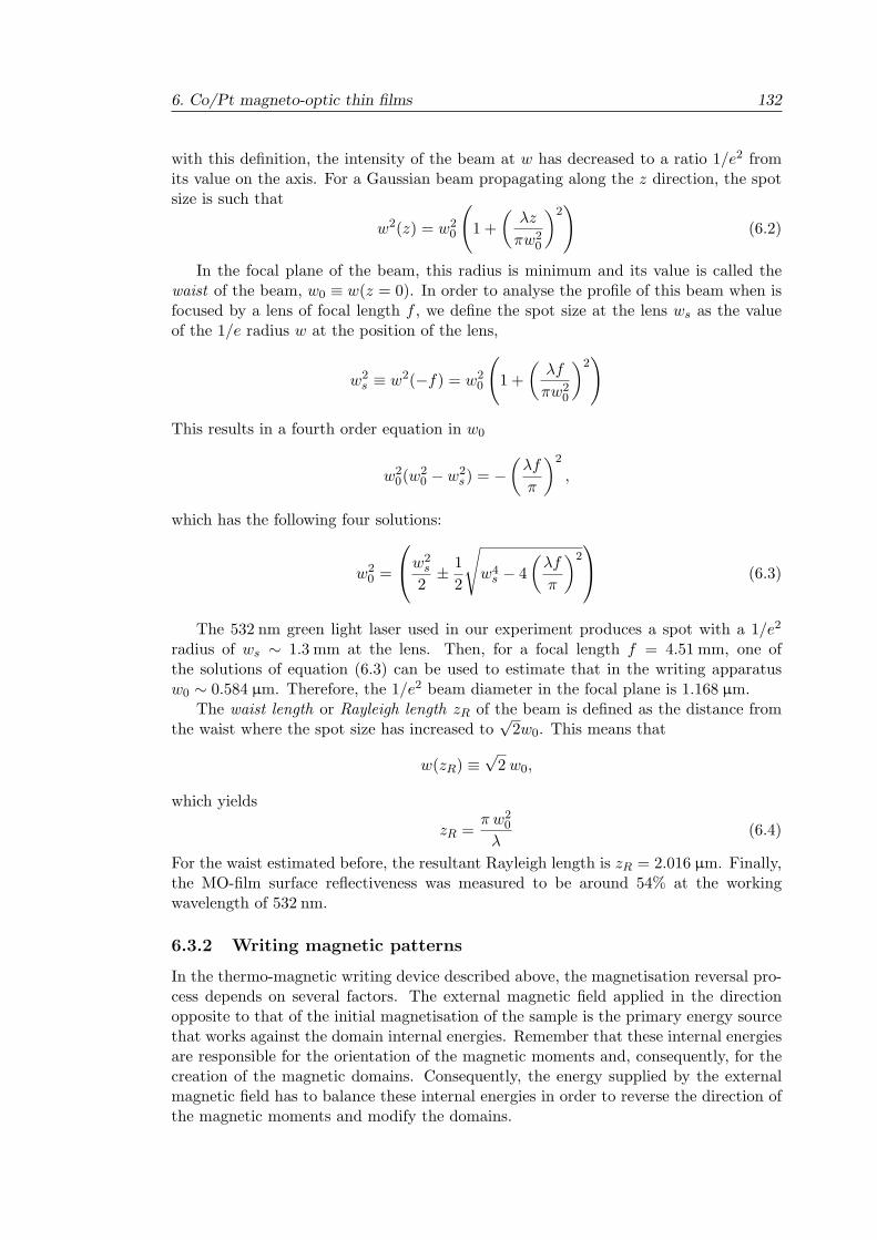
6. Co/Pt magneto-optic thin films 132
with this definition, the intensity of the beam at w has decreased to a ratio 1/e2 fromits value on the axis. For a Gaussian beam propagating along the z direction, the spotsize is such that
w2(z) = w20
81 +
)%z
&w20
*29
(6.2)
In the focal plane of the beam, this radius is minimum and its value is called thewaist of the beam, w0 & w(z = 0). In order to analyse the profile of this beam when isfocused by a lens of focal length f , we define the spot size at the lens ws as the valueof the 1/e radius w at the position of the lens,
w2s & w2("f) = w2
0
81 +
)%f
&w20
*29
This results in a fourth order equation in w0
w20(w
20 " w2
s) = ")
%f
&
*2
,
which has the following four solutions:
w20 =
!
"w2s
2± 1
2
/
w4s " 4
)%f
&
*2#
$ (6.3)
The 532 nm green light laser used in our experiment produces a spot with a 1/e2
radius of ws ! 1.3 mm at the lens. Then, for a focal length f = 4.51 mm, one ofthe solutions of equation (6.3) can be used to estimate that in the writing apparatusw0 ! 0.584 µm. Therefore, the 1/e2 beam diameter in the focal plane is 1.168 µm.
The waist length or Rayleigh length zR of the beam is defined as the distance fromthe waist where the spot size has increased to
%2w0. This means that
w(zR) &%
2 w0,
which yields
zR =& w2
0
%(6.4)
For the waist estimated before, the resultant Rayleigh length is zR = 2.016 µm. Finally,the MO-film surface reflectiveness was measured to be around 54% at the workingwavelength of 532 nm.
6.3.2 Writing magnetic patterns
In the thermo-magnetic writing device described above, the magnetisation reversal pro-cess depends on several factors. The external magnetic field applied in the directionopposite to that of the initial magnetisation of the sample is the primary energy sourcethat works against the domain internal energies. Remember that these internal energiesare responsible for the orientation of the magnetic moments and, consequently, for thecreation of the magnetic domains. Consequently, the energy supplied by the externalmagnetic field has to balance these internal energies in order to reverse the direction ofthe magnetic moments and modify the domains.
6. Co/Pt magneto-optic thin films 133
The laser beam is used to locally decrease the coercivity of the film. Thermalagitation acts against the orienting e"ect of the exchange field energy. Hence, the laserbeam intensity is also an important parameter that has to be taken into account duringthe process of thermo-magnetic writing. As a matter of fact, the laser intensity is soimportant that small displacements of the film surface from the focal plane of the beamare enough to prevent any writing on it.
Additionally, the temperature increase of a region of a film is a function of the timethat the beam spends on it or near it. Due to the displacement of the film during thewriting process, the time that a section of area of the film is illuminated by the laserdepends on the velocity of the translation stage. Once that the beam has transmittedenergy to the surface of the film and produced certain amount of heating, the energydi"uses through the crystal structure of the film.
6.4 Magnetic patterns
We have successfully written two di"erent patterns on the surface of our Co/Pt films.Figure 6.6 shows a section of the first pattern, an array of parallel lines. The secondpattern, shown in figure 6.8, is analogous to a wire Z-trap. A step-like pattern basedon a 40# 40 µm2 square is the elementary brick that builds up this periodic structure.
The images given in figures 6.6(a) and 6.8 (b) correspond to Magnetic Force Mi-croscope (MFM) measurements of the magnetic patterns. The MFM is a powerful toolfor analysing the small-scale features of a magnetised surface; it measures changes inthe vibration of a magnetic tip induced by the gradient of the force that the magnetisedsurface exerts on it. This tip is magnetised and held by a cantilever that sustains thetip vibration near its resonance frequency. Simultaneously, the vibrating tip closelyscans the surface of the film. Then, the tiny vibration of the tip is registered by a laserbeam that is reflected on its upper surface. After this reflection, the beam reaches aphoto-detector that measures the changes of the vibration of the tip. The resolutionof this microscope allows us to detect sub-micron features. Consequently, this device isthe main tool used in the analysis of the written patterns.
A set of 100 lines is particularly representative of my work. A reverse field of 500 G,a laser power of 74.7 mW and a translation speed of 0.25 m · s"1 were used to writethese lines. This is equivalent to the magnetic mirror described in [29]. The MFMmeasurement of this pattern (figure 6.6(a)) shows that these lines are ! 1 µm wide andare 2 µm away from each other. In addition, in this case each line was 200 µm long. Toanalyse the periodicity of this array, I have taken a single line of pixels perpendicularto the written lines, as indicated by the vertical red line included in the middle of theMFM image. The result of this is given in the graph (b) in figure 6.6. The nearly squaresteps demonstrate that each line is fully magnetised in a single direction and that, atthe border of these lines, the magnetisation is reversed in a thin section of surface thatis not wider than 200 nm. The Fourier transform of the plot given in figure 6.6(b) canbe used to determine the period of the array of lines. This is shown in graph (c), figure6.6. The narrow peak clearly indicates that the period % of this array is ! 2 µm
An additional feature of these lines can be seen in figure 6.6(a) and in more detailin figure 6.7(a). The edges of the lines, which are the boundaries between regions ofopposite magnetisation, are not straight. On the contrary, they oscillate along the linedirection creating a jagged boundary between regions of opposite magnetisation. Theinset shown in figure 6.6(a) is an MFM measurement of the unmagnetised MO film
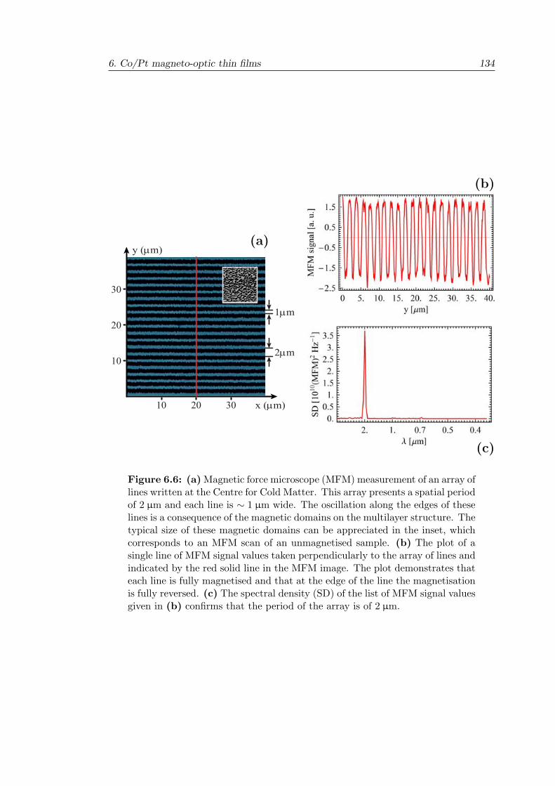
6. Co/Pt magneto-optic thin films 134
(a)
10 20 30
10
20
30
x (µm)
y (µm)
1µm
2µm
(b)
(c)
Figure 6.6: (a) Magnetic force microscope (MFM) measurement of an array oflines written at the Centre for Cold Matter. This array presents a spatial periodof 2 µm and each line is ! 1 µm wide. The oscillation along the edges of theselines is a consequence of the magnetic domains on the multilayer structure. Thetypical size of these magnetic domains can be appreciated in the inset, whichcorresponds to an MFM scan of an unmagnetised sample. (b) The plot of asingle line of MFM signal values taken perpendicularly to the array of lines andindicated by the red solid line in the MFM image. The plot demonstrates thateach line is fully magnetised and that at the edge of the line the magnetisationis fully reversed. (c) The spectral density (SD) of the list of MFM signal valuesgiven in (b) confirms that the period of the array is of 2 µm.
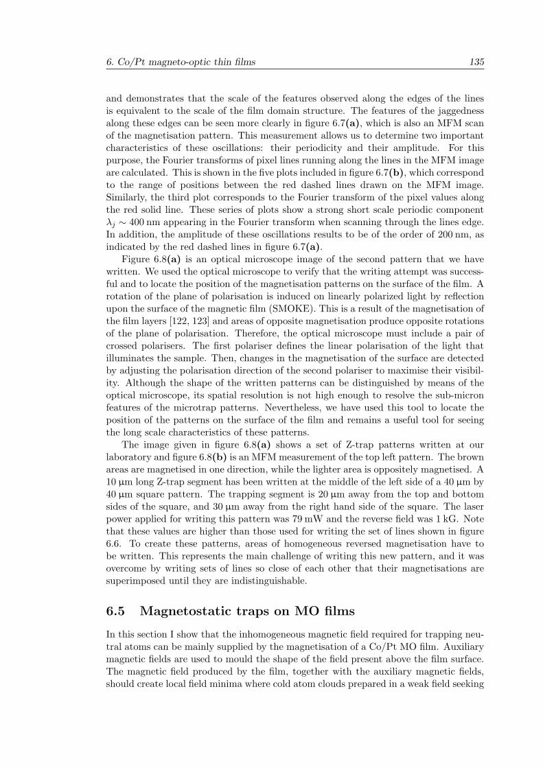
6. Co/Pt magneto-optic thin films 135
and demonstrates that the scale of the features observed along the edges of the linesis equivalent to the scale of the film domain structure. The features of the jaggednessalong these edges can be seen more clearly in figure 6.7(a), which is also an MFM scanof the magnetisation pattern. This measurement allows us to determine two importantcharacteristics of these oscillations: their periodicity and their amplitude. For thispurpose, the Fourier transforms of pixel lines running along the lines in the MFM imageare calculated. This is shown in the five plots included in figure 6.7(b), which correspondto the range of positions between the red dashed lines drawn on the MFM image.Similarly, the third plot corresponds to the Fourier transform of the pixel values alongthe red solid line. These series of plots show a strong short scale periodic component%j ! 400 nm appearing in the Fourier transform when scanning through the lines edge.In addition, the amplitude of these oscillations results to be of the order of 200 nm, asindicated by the red dashed lines in figure 6.7(a).
Figure 6.8(a) is an optical microscope image of the second pattern that we havewritten. We used the optical microscope to verify that the writing attempt was success-ful and to locate the position of the magnetisation patterns on the surface of the film. Arotation of the plane of polarisation is induced on linearly polarized light by reflectionupon the surface of the magnetic film (SMOKE). This is a result of the magnetisation ofthe film layers [122, 123] and areas of opposite magnetisation produce opposite rotationsof the plane of polarisation. Therefore, the optical microscope must include a pair ofcrossed polarisers. The first polariser defines the linear polarisation of the light thatilluminates the sample. Then, changes in the magnetisation of the surface are detectedby adjusting the polarisation direction of the second polariser to maximise their visibil-ity. Although the shape of the written patterns can be distinguished by means of theoptical microscope, its spatial resolution is not high enough to resolve the sub-micronfeatures of the microtrap patterns. Nevertheless, we have used this tool to locate theposition of the patterns on the surface of the film and remains a useful tool for seeingthe long scale characteristics of these patterns.
The image given in figure 6.8(a) shows a set of Z-trap patterns written at ourlaboratory and figure 6.8(b) is an MFM measurement of the top left pattern. The brownareas are magnetised in one direction, while the lighter area is oppositely magnetised. A10 µm long Z-trap segment has been written at the middle of the left side of a 40 µm by40 µm square pattern. The trapping segment is 20 µm away from the top and bottomsides of the square, and 30 µm away from the right hand side of the square. The laserpower applied for writing this pattern was 79 mW and the reverse field was 1 kG. Notethat these values are higher than those used for writing the set of lines shown in figure6.6. To create these patterns, areas of homogeneous reversed magnetisation have tobe written. This represents the main challenge of writing this new pattern, and it wasovercome by writing sets of lines so close of each other that their magnetisations aresuperimposed until they are indistinguishable.
6.5 Magnetostatic traps on MO films
In this section I show that the inhomogeneous magnetic field required for trapping neu-tral atoms can be mainly supplied by the magnetisation of a Co/Pt MO film. Auxiliarymagnetic fields are used to mould the shape of the field present above the film surface.The magnetic field produced by the film, together with the auxiliary magnetic fields,should create local field minima where cold atom clouds prepared in a weak field seeking
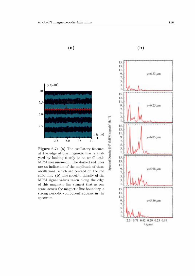
6. Co/Pt magneto-optic thin films 136
(a)
2.5 5.0 7.5
2.5
5.0
7.5
x (µm)
y (µm)
10
10
230nm
Figure 6.7: (a) The oscillatory featuresat the edge of one magnetic line is anal-ysed by looking closely at an small scaleMFM measurement. The dashed red linesare an indication of the amplitude of theseoscillations, which are centred on the redsolid line. (b) The spectral density of theMFM signal values taken along the edgeof this magnetic line suggest that as onescans across the magnetic line boundary, astrong periodic component appears in thespectrum.
(b)
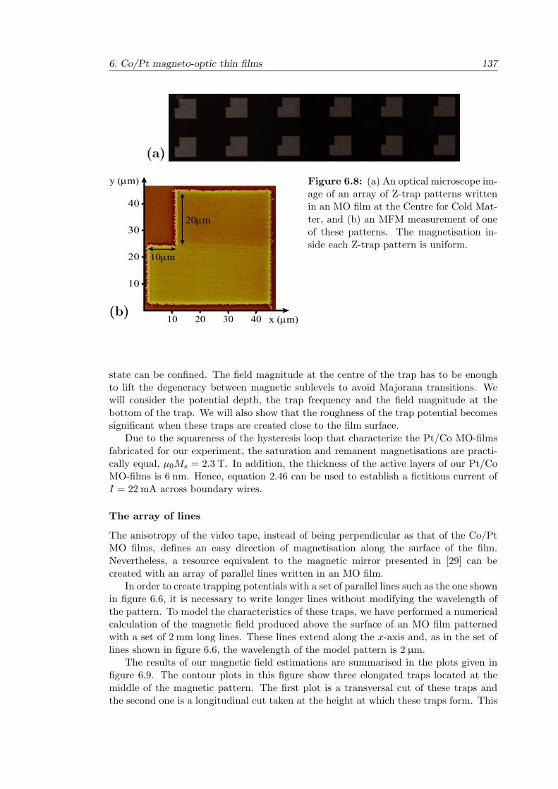
6. Co/Pt magneto-optic thin films 137
(a)
10 20 30 40
10
20
30
40
x (µm)
y (µm)
10µm
20µm
(b)
Figure 6.8: (a) An optical microscope im-age of an array of Z-trap patterns writtenin an MO film at the Centre for Cold Mat-ter, and (b) an MFM measurement of oneof these patterns. The magnetisation in-side each Z-trap pattern is uniform.
state can be confined. The field magnitude at the centre of the trap has to be enoughto lift the degeneracy between magnetic sublevels to avoid Majorana transitions. Wewill consider the potential depth, the trap frequency and the field magnitude at thebottom of the trap. We will also show that the roughness of the trap potential becomessignificant when these traps are created close to the film surface.
Due to the squareness of the hysteresis loop that characterize the Pt/Co MO-filmsfabricated for our experiment, the saturation and remanent magnetisations are practi-cally equal, µ0Ms = 2.3 T. In addition, the thickness of the active layers of our Pt/CoMO-films is 6 nm. Hence, equation 2.46 can be used to establish a fictitious current ofI = 22 mA across boundary wires.
The array of lines
The anisotropy of the video tape, instead of being perpendicular as that of the Co/PtMO films, defines an easy direction of magnetisation along the surface of the film.Nevertheless, a resource equivalent to the magnetic mirror presented in [29] can becreated with an array of parallel lines written in an MO film.
In order to create trapping potentials with a set of parallel lines such as the one shownin figure 6.6, it is necessary to write longer lines without modifying the wavelength ofthe pattern. To model the characteristics of these traps, we have performed a numericalcalculation of the magnetic field produced above the surface of an MO film patternedwith a set of 2 mm long lines. These lines extend along the x-axis and, as in the set oflines shown in figure 6.6, the wavelength of the model pattern is 2 µm.
The results of our magnetic field estimations are summarised in the plots given infigure 6.9. The contour plots in this figure show three elongated traps located at themiddle of the magnetic pattern. The first plot is a transversal cut of these traps andthe second one is a longitudinal cut taken at the height at which these traps form. This
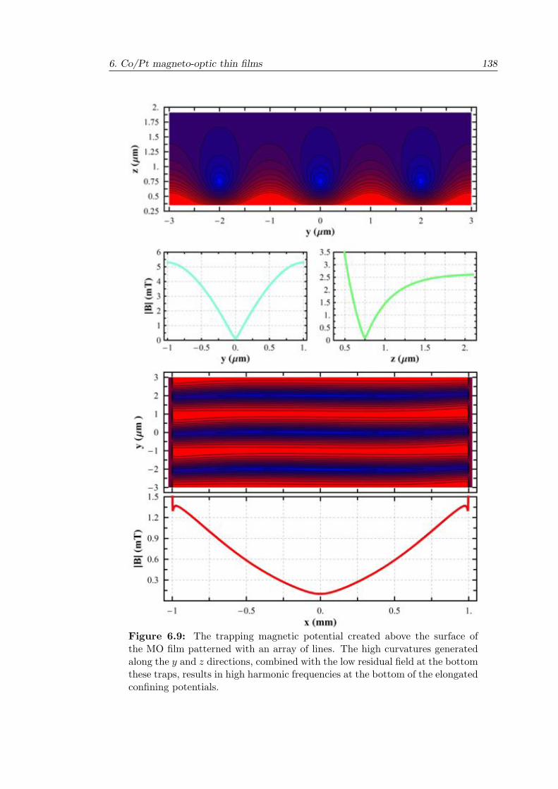
6. Co/Pt magneto-optic thin films 138
Figure 6.9: The trapping magnetic potential created above the surface ofthe MO film patterned with an array of lines. The high curvatures generatedalong the y and z directions, combined with the low residual field at the bottomthese traps, results in high harmonic frequencies at the bottom of the elongatedconfining potentials.
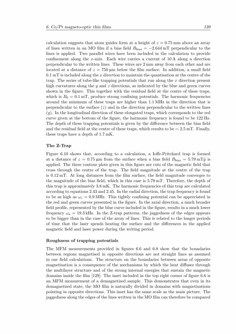
6. Co/Pt magneto-optic thin films 139
calculation suggests that atom guides form at a height of z = 0.75 mm above an arrayof lines written in an MO film if a bias field Bbias = "2.644 mT perpendicular to thelines is applied. Two parallel wires have been included in the calculation to provideconfinement along the x-axis. Each wire carries a current of 10 A along a directionperpendicular to the written lines. These wires are 2 mm away from each other and arelocated at a distance of z = 750 µm below the film surface. In addition, a small field0.1 mT is included along the x direction to maintain the quantisation at the centre of thetrap. The series of tube-like trapping potentials that run along the x direction presenthigh curvatures along the y and z directions, as indicated by the blue and green curvesshown in the figure. This together with the residual field at the centre of these traps,which is B0 = 0.1 mT, produce strong confining potentials. The harmonic frequenciesaround the minimum of these traps are higher than 1.1 MHz in the direction that isperpendicular to the surface (z) and in the direction perpendicular to the written lines(y). In the longitudinal direction of these elongated traps, which corresponds to the redcurve given at the bottom of the figure, the harmonic frequency is found to be 122 Hz.The depth of these trapping potentials is given by the di"erence between the bias fieldand the residual field at the centre of these traps, which results to be ! 2.5 mT. Finally,these traps have a depth of 1.7 mK.
The Z-Trap
Figure 6.10 shows that, according to a calculation, a Io"e-Pritchard trap is formedat a distance of z = 0.75 µm from the surface when a bias field Bbias = 5.79 mTy isapplied. The three contour plots given in this figure are cuts of the magnetic field thatcross through the centre of the trap. The field magnitude at the centre of the trapis 0.12 mT. At long distances from the film surface, the field magnitude converges tothe magnitude of the bias field, which in this case is 5.79 mT. Therefore, the depth ofthis trap is approximately 3.8 mK. The harmonic frequencies of this trap are calculatedaccording to equations 2.43 and 2.45. In the radial direction, the trap frequency is foundto be as high as )r = 0.9 MHz. This tightly confining potential can be appreciated inthe red and green curves presented in the figure. In the axial direction, a much broaderfield profile, represented by the blue curve included in the figure, results in a much lowerfrequency )a = 19.3 kHz. In the Z-trap patterns, the jaggedness of the edges appearsto be bigger than in the case of the array of lines. This is related to the longer periodsof time that the laser spends heating the surface and the di"erences in the appliedmagnetic field and laser power during the writing period.
Roughness of trapping potentials
The MFM measurements provided in figures 6.6 and 6.8 show that the boundariesbetween regions magnetised in opposite directions are not straight lines as assumedin our field calculations. The structure on the boundaries between areas of oppositemagnetisation is a consequence of the mechanisms by which the heat di"uses throughthe multilayer structure and of the strong internal energies that sustain the magneticdomains inside the film [129]. The inset included in the top right corner of figure 6.6 isan MFM measurement of a demagnetised sample. This demonstrates that even in itsdemagnetised state, the MO film is naturally divided in domains with magnetisationspointing in opposite directions. This inset has the same scale as the main picture. Thejaggedness along the edges of the lines written in the MO film can therefore be compared
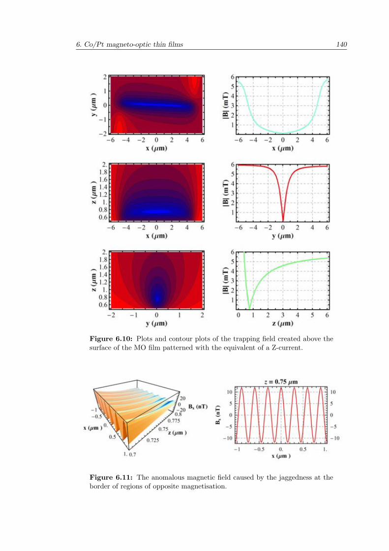
6. Co/Pt magneto-optic thin films 140
Figure 6.10: Plots and contour plots of the trapping field created above thesurface of the MO film patterned with the equivalent of a Z-current.
Figure 6.11: The anomalous magnetic field caused by the jaggedness at theborder of regions of opposite magnetisation.
6. Co/Pt magneto-optic thin films 141
with the characteristic length scale of the domains in the unmagnetised sample. Thiscomparison suggests that the quality of the magnetisation patterns created in the Co/PtMO films is limited by the size of the magnetic domains formed in the material.
As a result of the boundary jaggedness, the fictitious currents oscillate in the planeof the film. As we reported in [76] (see Appendix E), the analysis of our MFM mea-surements has allowed us to estimate that the typical amplitude of these oscillations isaj = 125 nm and the typical wavelength is %j = 300 nm. Previous work in our grouphas demonstrated that the anomalous field generated in the vicinity of a current carry-ing wire can be represented with a periodic function multiplied by the modified Besselfunction [58]. An example of such anomalous field is shown in figure 6.11. The oscil-lation of the fictitious currents in the MO films is analogous to the anomalous currentgenerated by a wire. In consequence, we have proposed that at a height z , aj abovethe boundary of two regions with opposite magnetisations the main field component isgiven by
By + µ0I/2&z
Meanwhile, the transverse oscillations along the edges of the magnetic patterns producea field which here we approximated by an oscillating field along the wire
Bx +µ0I
2&k2aK1(kz) cos(kx)
where k = 2&/%j and K1 is the modified Bessel function.As demonstrated in figure 6.11, the magnetic field generated by this idealised anoma-
lous oscillation of the pattern boundaries has an amplitude at the trapping heightz = 0.75 µm of 24 nT. This corresponds to corrugations in the trapping potentialwith a characteristic depth of 16 nK. To get an idea of what this means in terms ofthe latest advances on cold atoms research, let us compare this depth with the chemicalpotential µ of a BEC. According to Ketterle et al. [24],
µ =4&na!2
m(6.5)
where n is the condensate density; a is the s-wave scattering length; and m is the massof the atom. For a 87Rb condensate, n is typically 1014 atoms/cm3, and a + 100a0, witha0 = 0.529 A. This leads us to a chemical potential of µ/kB + 37 nK. Although thisvalue is higher than the potential depth estimated for the corrugations in the trappingpotential, these values are of the same order of magnitude and is reasonable to believethat a Bose-Einstein condensate confined in these traps would exhibit fragmentation atsuch short distances from the film surface.
6.6 Pyramids and MO films
The Co-Pt multilayer thin films can also be combined with the micro-pyramids presentedin the previous chapter; the multilayer film in this case would be used as the primarysource of magnetic field for generating the magneto-optic traps. A new procedure forselectively etching small areas of a Co-Pt multilayer thin film, without substantiallymodifying its magnetic properties, has been demonstrated. The Co-Pt multilayer struc-ture of these Magneto-Optic (MO) films was deposited on a silicon under layer. Theetching process used to make apertures in the MO film leaves this under layer unaf-fected. Hence, a further process of chemical etching can be applied to these substrates
6. Co/Pt magneto-optic thin films 142
in order to create micrometric pyramids on the silicon under layer. Finally, a thin re-flective coating can be deposited on top of the array of pyramids and the remaining MOfilm.
Due to the perpendicular magnetisation of the Co-Pt multilayer structure, the mag-netic field created at an aperture made on them can be thought as that produced bya single closed loop. The corresponding magnetic field circulates around the fictitiouscurrent loop and right at the surface it is always perpendicular to the film. Conse-quently, an external magnetic field can be applied in order to create and move a pointof zero magnetic field strength along the axis of each aperture. In addition, due to thesmall scale of these features and the strong remanent magnetization of the MO film,high gradients can be produced in the region of the hollow pyramid. Therefore, it isjustified to believe that magneto-optic traps can be created with these resources.
Let us consider a saturation magnetisation µ0MS = 2.3 T/m and a cobalt totalthickness t = 6 nm (see figures 6.3 and 6.1 in pages 128 and 125 respectively). Then,with the aid of equation 2.46 (page 40) we estimate that the fictitious current runningthrough the edge of a square aperture made on the MO film is 11 mA. If we nowsubstitute this value in equation 2.46, we find that to obtain a gradient of 20 G/cm weneed to create a square opening and a silicon pyramid with a side length of approximately300 µm. This length scale is well within the fabrication capabilities of the techniquesdescribed at the beginning of chapter 5.
6.7 Summary
Here I have shown that the remanent field generated by the Co/Pt MO films is as highas 2.3 T. This is ten times higher than the one that is present above the video tape atomchip used in the work reported by Sinclair et al. [68, 67]. In addition, I have shown thatthe periodic patterns written on the surface of the MO films have features of just a coupleof micrometres. Compared to the patterns that have been utilised in the video tapeexperiments, which have a period of approximately 100 µm, the Co/Pt films representan important improvement in the development of atom chips based on permanentlymagnetised media. This is reflected in the numerical calculations of the micro trapsthat have been presented in this chapter and reported in [76] (see appendix E), wherethe resulting trapping frequencies have been estimated to be as high as one megahertzin the radial direction and several hundred kilohertz in the longitudinal direction.
As a result of the domain structure of the Co/Pt films, on the edges of the writtenpatterns we have observed features with a length scale on the order of hundreds ofnanometres. We have estimated that these features would produce corrugations in thetrapping field. For an atom cloud located at distance of 750 nm from the surface of thefilm, we calculated that these corrugations would have a characteristic depth of 16 nK.These kind of corrugations have also been observed in the video tape micro traps, but inthis case these appeared as far as 50 µm away from the chip surface and had potentialdepths of up to 1 µK.
This work has demonstrated the potential that MO films have for creating coldatom micro traps. In spite of this, an atom chip based on this technology has not yetbeen fabricated and loaded into a cold atom experiment. Our numerical estimationsallowed us to predict the details of the interaction between a cold atom cloud and thefield generated above the Co/Pt MO films. These results are su!cient for establish-ing the adequacy of this technology. In conclusion, Co/Pt magneto-optical thin films

6. Co/Pt magneto-optic thin films 143
are presented in this chapter as a powerful tool that can be incorporated into futuregenerations of atom chips. For instance, we have proposed that an atom chip com-bining micro-fabricated optical components, such as hollow pyramidal mirrors, and apermanently magnetised medium like the Co-Pt magneto-optic film can be fabricated.
144
Chapter 7
Conclusions
We have built an experimental apparatus for testing new generations of atom chips.This apparatus consists of a vacuum system, three laser light sources, magnetic fieldsources, and an imaging system. The vacuum chamber is characterised by a largeinternal volume and wide optical axis. Sets of coils for the generation of the magneticfields required for creating magneto-optic traps in macroscopic hollow pyramidal mirrorshave been designed, built, and incorporated to the experimental apparatus. In addition,coils for balancing stray fields and for manipulating the position of the MOT were alsoincluded in the experimental apparatus.
Three external cavity diode lasers were incorporated to the experimental appara-tus. The optics and electronic devices required for locking these lasers, as well as forpreparing and delivering the laser beams to the main experimental chamber were alsobuilt. Locking signals for the three lasers are derived from Doppler free polarizationspectrums and a dichroic-atomic-vapor laser lock (DAVLL). The first scheme providesan stable frequency reference for determining the detuning of the trapping light. Thetwo DAVLL locks provide in addition the means for tuning the trapping and repumplight.
We have demonstrated that in spite of the angle di"erence between a 90! pyramidand the 70.5! of chemically etched pyramids on silicon wafers, the latter are still capableof generating magneto-optical traps. For this we fabricated on glass two pyramidalhollow mirrors, the first with an angle of 70.5! between its opposing faces and the secondone with an angle of 90!. The side length of these two pyramids is approximately 16 mm.To identify possible causes of imbalance in the MOT forces as a result of the pyramidalgeometry generated in silicon, the optical properties of the these pyramids were carefullystudied, both numerically and experimentally. We found that the pyramid surfacesections located next to the edges of the pyramid faces are responsible for the generationof light rays with the wrong polarisation. After going through three reflections, theselight component cross through the pyramid axis creating a force imbalance that issu!cient for destroying the trap.
In view of these results, we have identified methods for reducing and eliminating theundesired e"ect of these light sections. First, as this light su"ers one more reflection
7. Conclusions 145
from the pyramid faces than the rest of the light components contributing to the trap,we proposed to use a limited reflectivity coating in the pyramid faces. This way, wefound that an aluminium based coating characterised by a reflectivity of 78% takescare e!ciently of the imbalance generated by these parasitic light components. Wedemostrated that as many as 107 rubidium atoms can be trapped in our 70.5! glasspyramid coated in aluminium. We compared the MOTs generated in this pyramidwith the one formed in the 90! pyramid, both of comparable sizes and both coatedwith aluminium, and found no appreciable di"erences in the MOTs generated in thesetwo pyramids. A summary of these results and a complete optical characterisation ofthe 70.5! pyramidal geometry has been published in [72] and this paper is included inappendix C.
We have also shown that the undesired reflections generated in a 70.5! pyramid canbe eliminated if the surface of the pyramid is appropriately masked during the depositionof the reflective coating. The regions where the undesired reflections originate, whichwere identified by means of a ray tracing analysis, can be covered with these masks.This method gives satisfactory results when a high reflectivity gold coating (0 ! 95 %)is deposited in the regions not covered by the masks.
We measured scaling laws for the parameters that determine the MOT dynamics in70.5! pyramids. We found that the number of atoms that can be trapped on pyramidsof di"erent sizes is mainly determined by the MOT capture rate. As anticipated insection 2.4.1, the change of the capture parameter with the pyramid dimensions canbe described by means of a power law. To begin with, a measurement of the capturerate far from the pyramid apex allowed us to corroborate the validity of this powerlaw. Based on this measurement, we suggested that the perpendicular distance fromthe MOT centre to the pyramid surface is the defining distance on the operation ofthese MOTs. Next, the experiments performed in the vicinity of the pyramid apexalso resulted in a power law dependence of the capture rate on the distance to thepyramid apex. In this case we found that the capture rate divided by the rubidiumvapour density, which we denoted as $, is proportional to h3.5(3), h being the distancebetween the cold atom cloud and the apex of the pyramid. Also, our experiments haveshown that the loss rate parameter is practically insensitive to the size of the pyramidas long as the trap to surface distance is > 600 µm. Below this limit, we found thatthe increase in the loss rate can be appropriately described by considering that thecloud remains in the temperature limited regime and that atoms colliding with theroom temperature pyramid surface are irremediably lost from the trap. Based on thesescaling law measurements, we concluded that on the order of 104 atoms can be trappedin pyramids with a 1.2 mm side length, and some tens of atoms can be trapped in200 µm side length pyramids.
In this thesis I have presented an atom chip that integrates pyramidal micro-mirrorsand sources of magnetic field. Standard silicon micro-fabrication techniques have beenused to create an array of pyramidal pits, which coated with the appropriate metallicmaterial, can create high quality optical components on the chip surface. I have given acomplete characterisation of the resulting micro-mirrors, including their most relevantphysical and optical properties. These micro-fabricated optical components have beencombined with surface mounted wires to create a hybrid new device. In this chip, squarecurrent currying wire loops run around the pyramid apertures. Then, the magnetic fieldgenerated by these loops can be complemented with an homogeneous magnetic biasfield perpendicular to the chip surface. With the right choice of current and bias field
7. Conclusions 146
magnitude, spherical quadrupole potentials are created inside the atom chip pyramids.Both the reflective coating and the wires are made of gold. Hence, the masked coatingof the pyramid faces that was tested in the glass 70.5! was recreated in the atom chipfabrication.
I have described how the pyramid atom chip was mounted and bond wired in aCPGA chip mount. Extensive thermal, electric, magnetic and vacuum compatibilitycharacterisations of the full chip arrangement have been carried out. Vacuum testsand magnetic field estimations and measurements have been performed with the aim ofestablishing the conditions under which the chip mount elements can be used. We havedemonstrated that pressures below 10"9 mbar can be achieved in a vacuum system inwhich a set composed by a ceramic pin grid array (CPGA), a sockets array and a printedcircuit board has been loaded. Also, it has been verified under which circumstancesthe stray magnetic field generated above the chip carrier is low enough to allow thecreation of the micro-MOTs. In particular, we found that in order to keep the straymagnetic field generated in the chip attachment area of the CPGA at an acceptablelevel, it is necessary to remove the nickel layer present in this area. A paper thatdescribes the pyramid atom chip fabrication procedure and the characterisation of thefull packaging solution has been recently accepted for publication in the Journal ofMicroelectromechanical Systems. This paper (see reference [109]) has been included inappendix D.
Co/Pt magneto optic thin films have been fabricated with the aim of determininghow suitable is this media for creating a permanently magnetised atom chip. I haveshown that these films are characterised by a large perpendicular anisotropy, a highremanent magnetisation, a large room temperature coercivity, and the squareness ratioof its hysteresis loop is close to one. Then, a thermo-magnetic writing apparatus wasbuilt and magnetic patterns for creating local field minima were successfully created onthe surface of these films. We have demonstrated that atomic micro-traps based on thesemagnetic patterns can be produced. The large remanent magnetisation of these films,given by µ0Ms = 2.3 T, combined with micron-sized features, permit trap frequenciesof up to 1.1 MHz. In addition, the high room-temperature coercivity of these films notonly allows the creation of well defined micron sized magnetic patterns, but also assuresthat the patterns will remain intact even under the influence of an external magneticfield. This represents an important improvement with respect to the performance of thevideo tape atom chip.
Two magnetic patterns have been written in the Co/Pt MO films. An array of linescan be used to create a series of elongated atom traps above the chip surface. The secondpattern consists of an array of Z-traps, which can be used to create cigar shaped trapsabove the film surface. These patterns were carefully analysed via optical and magneticforce microscopy. These patterns consist of well defined and uniformly magnetised areasin which the direction of the magnetisation vector was reversed. The borders betweenregions magnetised in opposite directions present jaggedness, which we have shown to bea result of the film domain structure. As a consequence of this, the trapping potentialsgenerated above these films would have a corrugated structure. We have estimated thatthis corrugation would produce 16 nK deep wells at the bottom of a trapping potentiallocated 0.75 µm above the film surface. Although lower than the self interaction energyof atoms in a BEC (! 40 nK), this potential wells could generate fragmentation of theatom cloud. The results presented in this thesis allowed us to estimate the performanceof the Co/Pt in atom optics applications so accurately that we decided not to attempt
7. Conclusions 147
loading an atom chip made exclusively of this magnetic material into a cold atomsexperiment. However, these MO films remain as a an extremely versatile and powerfultool for more complicated atom optics devices. Further optimisation of these MO filmswould require a reduction of the length scale of their domain structure with maintainingboth the strong remanent magnetisation, and the large coercivity that characterise thesemagnetic films. The most important results of this investigation were published in [76].This paper is included in appendix E.
This thesis concludes with the fabrication of the first pyramid atom chip and itsincorporation into the experimental apparatus. Naturally, the steps that follow in thisresearch project include testing the functioning of this atom chip and determining itsoptimal operation parameters. Therefore, the creation of magneto optical traps on thesurface of this atom chip is being currently investigated at the Centre for Cold Matter.At the time of writing this thesis, no atoms have been observed in the atom chip pyra-mids. The causes for this are been investigated in order to optimise loading and imagingsystems, and even the micro fabrication process. Once that MOTs have been producedin the atom chip pyramids, it will be necessary to determine the currents required foroptimal operation of each one of the various pyramid side lengths included in this atomchip. This information results particularly interesting because it will determine thepossibility of integrating both micro-fabricated pyramids and magneto-optic thin filmsin a future atom chip. An additional feature of these micro-MOTs that would need tobe properly characterised is their sensitivity to magnetic fields. It has been proposedthat a highly sensitive magnetometer can be fabricated utilising these micro-fabricatedpyramid MOTs. We have shown that the cold atom clouds magneto-optically collectedin these pyramids could then be held by a purely magnetic trap. Consequently, a furthergoal of this research would be to magnetically trap these atom clouds and extract themfrom the pyramids internal volume. These clouds would then be held by a mirror imageof the magnetic quadrupole potential generated inside the pyramids.
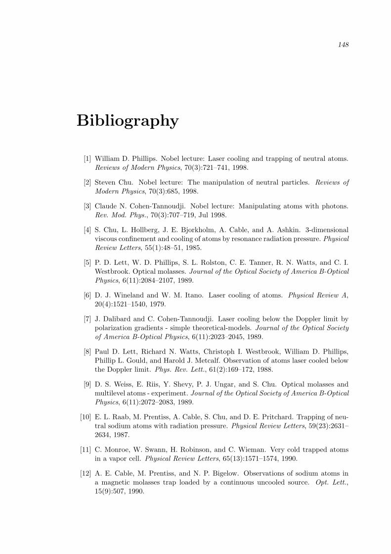
148
Bibliography
[1] William D. Phillips. Nobel lecture: Laser cooling and trapping of neutral atoms.Reviews of Modern Physics, 70(3):721–741, 1998.
[2] Steven Chu. Nobel lecture: The manipulation of neutral particles. Reviews ofModern Physics, 70(3):685, 1998.
[3] Claude N. Cohen-Tannoudji. Nobel lecture: Manipulating atoms with photons.Rev. Mod. Phys., 70(3):707–719, Jul 1998.
[4] S. Chu, L. Hollberg, J. E. Bjorkholm, A. Cable, and A. Ashkin. 3-dimensionalviscous confinement and cooling of atoms by resonance radiation pressure. PhysicalReview Letters, 55(1):48–51, 1985.
[5] P. D. Lett, W. D. Phillips, S. L. Rolston, C. E. Tanner, R. N. Watts, and C. I.Westbrook. Optical molasses. Journal of the Optical Society of America B-OpticalPhysics, 6(11):2084–2107, 1989.
[6] D. J. Wineland and W. M. Itano. Laser cooling of atoms. Physical Review A,20(4):1521–1540, 1979.
[7] J. Dalibard and C. Cohen-Tannoudji. Laser cooling below the Doppler limit bypolarization gradients - simple theoretical-models. Journal of the Optical Societyof America B-Optical Physics, 6(11):2023–2045, 1989.
[8] Paul D. Lett, Richard N. Watts, Christoph I. Westbrook, William D. Phillips,Phillip L. Gould, and Harold J. Metcalf. Observation of atoms laser cooled belowthe Doppler limit. Phys. Rev. Lett., 61(2):169–172, 1988.
[9] D. S. Weiss, E. Riis, Y. Shevy, P. J. Ungar, and S. Chu. Optical molasses andmultilevel atoms - experiment. Journal of the Optical Society of America B-OpticalPhysics, 6(11):2072–2083, 1989.
[10] E. L. Raab, M. Prentiss, A. Cable, S. Chu, and D. E. Pritchard. Trapping of neu-tral sodium atoms with radiation pressure. Physical Review Letters, 59(23):2631–2634, 1987.
[11] C. Monroe, W. Swann, H. Robinson, and C. Wieman. Very cold trapped atomsin a vapor cell. Physical Review Letters, 65(13):1571–1574, 1990.
[12] A. E. Cable, M. Prentiss, and N. P. Bigelow. Observations of sodium atoms ina magnetic molasses trap loaded by a continuous uncooled source. Opt. Lett.,15(9):507, 1990.
BIBLIOGRAPHY 149
[13] K. E. Gibble, S. Kasapi, and S. Chu. Improved magnetooptic trapping in a vaporcell. Optics Letters, 17(7):526–528, 1992.
[14] Alan L. Migdall, John V. Prodan, William D. Phillips, Thomas H. Bergeman,and Harold J. Metcalf. First observation of magnetically trapped neutral atoms.Phys. Rev. Lett., 54(24):2596–2599, 1985.
[15] Wolfgang Paul. Electromagnetic traps for charged and neutral particles. Reviewsof Modern Physics, 62(3):531–540, 1990.
[16] T. Bergeman, G. Erez, and H. J. Metcalf. Magnetostatic trapping fields for neutralatoms. Physical Review A, 35(4):1535–1546, 1987.
[17] H. Metcalf. Magneto-optical trapping and its application to helium metastables.Journal of the Optical Society of America B-Optical Physics, 6(11):2206–2210,1989.
[18] M. H. Anderson, J. R. Ensher, M. R. Matthews, C. E. Wieman, and E. A. Cornell.Observation of Bose-Einstein condensation in a dilute atomic vapor. Science,269(5221):198–201, 1995.
[19] C. C. Bradley, C. A. Sackett, J. J. Tollett, and R. G. Hulet. Evidence of Bose-Einstein condensation in an atomic gas with attractive interactions. Phys. Rev.Lett., 75(9):1687–1690, 1995.
[20] K. B. Davis, M. O. Mewes, M. R. Andrews, N. J. van Druten, D. S. Durfee, D. M.Kurn, and W. Ketterle. Bose-Einstein condensation in a gas of sodium atoms.Phys. Rev. Lett., 75(22):3969–3973, 1995.
[21] E. A. Cornell and C. E. Wieman. Nobel Lecture: Bose-Einstein condensation ina dilute gas, the first 70 years and some recent experiments. Rev. Mod. Phys.,74(3):875–893, 2002.
[22] Wolfgang Ketterle. Nobel lecture: When atoms behave as waves: Bose-einsteincondensation and the atom laser. Rev. Mod. Phys., 74(4):1131–1151, 2002.
[23] Eric A. Cornell, Jason R. Ensher, and Carl E. Wieman. Experiments in DiluteAtomic Bose-Einstein Condensation. arXiv:cond-mat/9903109v1, 1999.
[24] W. Ketterle, D.S. Durfee, , and D.M. Stamper-Kurn. Making, probing and un-derstanding Bose-Einstein condensates. arXiv:cond-mat/9904034v2, 1999.
[25] D. W. Sesko and C. E. Wieman. Observation of the cesium clock transition inlaser-cooled atoms. Optics Letters, 14(5):269–271, 1989.
[26] C. Monroe, H. Robinson, and C. Wieman. Observation of the cesium clock tran-sition using laser-cooled atoms in a vapor cell. Optics Letters, 16(1):50–52, 1991.
[27] C. Monroe. Quantum information processing with atoms and photons. Nature,416:238–246, 2002.
[28] D. Muller, D. Z. Anderson, R. J. Grow, P. D. D. Schwindt, and E. A. Cornell.Guiding neutral atoms around curves with lithographically patterned current-carrying wires. Physical Review Letters, 83(25):5194–5197, 1999.
BIBLIOGRAPHY 150
[29] E. A. Hinds and I. G. Hughes. Magnetic atom optics: mirrors, guides, traps, andchips for atoms. Journal of Physics D-Applied Physics, 32(18):R119–R146, 1999.
[30] R. Folman, P. Kruger, D. Cassettari, B. Hessmo, T. Maier, and J. Schmiedmayer.Controlling cold atoms using nanofabricated surfaces: Atom chips. Physical Re-view Letters, 84(20):4749–4752, 2000.
[31] D. Cassettari, A. Chenet, R. Folman, A. Haase, B. Hessmo, P. Kruger, T. Maier,S. Schneider, T. Calarco, and J. Schmiedmayer. Micromanipulation of neutralatoms with nanofabricated structures. Applied Physics B-Lasers and Optics,70(5):721–730, 2000.
[32] J. Fortagh, H. Ott, A. Grossmann, and C. Zimmermann. Miniaturized magneticguide for neutral atoms. Applied Physics B-Lasers and Optics, 70(5):701–708,2000.
[33] J. Reichel, W. Hansel, P. Hommelho", and T. W. Hansch. Applications of inte-grated magnetic microtraps. Applied Physics B-Lasers and Optics, 72(1):81–89,2001.
[34] J. D. Weinstein and K. G. Libbrecht. Microscopic magnetic traps for neutralatoms. Phys. Rev. A, 52(5):4004–4009, 1995.
[35] S. Eriksson, M. Trupke, H. F. Powell, D. Sahagun, C. D. J. Sinclair, E. A. Curtis,B. E. Sauer, E. A. Hinds, Z. Moktadir, C. O. Gollasch, and M. Kraft. Integratedoptical components on atom chips. European Physical Journal D, 35(1):135–139,2005.
[36] G. Birkl, F. B. J. Buchkremer, R. Dumke, and W. Ertmer. Atom optics withmicrofabricated optical elements. Optics Communications, 191(1-2):67–81, 2001.
[37] N. H. Dekker, C. S. Lee, V. Lorent, J. H. Thywissen, S. P. Smith, M. Drndic,R. M. Westervelt, and M. Prentiss. Guiding neutral atoms on a chip. PhysicalReview Letters, 84(6):1124–1127, 2000.
[38] D. Cassettari, B. Hessmo, R. Folman, T. Maier, and J. Schmiedmayer. Beamsplitter for guided atoms. Physical Review Letters, 85(26):5483–5487, 2000.
[39] A. E. Leanhardt, A. P. Chikkatur, D. Kielpinski, Y. Shin, T. L. Gustavson,W. Ketterle, and D. E. Pritchard. Propagation of Bose-Einstein condensatesin a magnetic waveguide. Physical Review Letters, 89(4):040401, 2002.
[40] E. A. Hinds, C. J. Vale, and M. G. Boshier. Two-wire waveguide and interferom-eter for cold atoms. Physical Review Letters, 86(8):1462–1465, 2001.
[41] H. Ott, J. Fortagh, G. Schlotterbeck, A. Grossmann, and C. Zimmermann.Bose-Einstein condensation in a surface microtrap. Physical Review Letters,87(23):230401, 2001.
[42] J. Reichel. Microchip traps and BoseEinstein condensation. Applied Physics B:Lasers and Optics, 75:469–487, 2002.
[43] W. Hansel, P. Hommelho", T. W. Hansch, and J. Reichel. Bose-Einstein conden-sation on a microelectronic chip. Nature, 413(6855):498–501, 2001.
BIBLIOGRAPHY 151
[44] S. Schneider, A. Kasper, Ch. vom Hagen, M. Bartenstein, B. Engeser, T. Schumm,I. Bar-Joseph, R. Folman, L. Feenstra, and J. Schmiedmayer. Bose-Einstein con-densation in a simple microtrap. Phys. Rev. A, 67(2):023612, 2003.
[45] A. Kasper, S. Schneider, C. vom Hagen, M. Bartenstein, B. Engeser, T. Schumm,I. Bar-Joseph, R. Folman, L. Feenstra, and J. Schmiedmayer. A Bose-Einsteincondensate in a microtrap. Journal of Optics B-Quantum and Semiclassical Op-tics, 5(2):S143–S149, 2003.
[46] H. Ott, J. Fortagh, S. Kraft, A. Gunther, D. Komma, and C. Zimmermann. Non-linear dynamics of a Bose-Einstein condensate in a magnetic waveguide. PhysicalReview Letters, 91(4):040402, 2003.
[47] H. Ott, J. Fortagh, and C. Zimmermann. Dynamics of a Bose-Einstein conden-sate in an anharmonic trap. Journal of Physics B-Atomic Molecular and OpticalPhysics, 36(13):2817–2822, 2003.
[48] J. Fortagh, H. Ott, S. Kraft, A. Gunther, and C. Zimmermann. Bose-Einstein con-densates in magnetic waveguides. Applied Physics B-Lasers and Optics, 76(2):157–163, 2003.
[49] R. Long, T. Steinmetz, P. Hommelho", W. Hansel, T. W. Hansch, and J. Reichel.Magnetic microchip traps and single-atom detection. Philosophical Transactionsof the Royal Society of London Series a-Mathematical Physical and EngineeringSciences, 361(1808):1375–1389, 2003.
[50] R. Long, T. Rom, W. Hansel, T. W. Hansch, and J. Reichel. Long distancemagnetic conveyor for precise positioning of ultracold atoms. European PhysicalJournal D, 35(1):125–133, 2005.
[51] Philipp Treutlein, Peter Hommelho", Tilo Steinmetz, Theodor W. Hansch,and Jakob Reichel. Coherence in microchip traps. Physical Review Letters,92(20):203005, 2004.
[52] C. Henkel, S. Potting, and M. Wilkens. Loss and heating of particles in small andnoisy traps. Applied Physics B-Lasers and Optics, 69(5-6):379–387, 1999.
[53] C. Henkel and S. Potting. Coherent transport of matter waves. Applied PhysicsB-Lasers and Optics, 72(1):73–80, 2001.
[54] M. P. A. Jones, C. J. Vale, D. Sahagun, B. V. Hall, and E. A. Hinds. Spincoupling between cold atoms and the thermal fluctuations of a metal surface.Physical Review Letters, 91(8):080401, 2003.
[55] C. Henkel, P. Kruger, R. Folman, and J. Schmiedmayer. Fundamental limitsfor coherent manipulation on atom chips. Applied Physics B-Lasers and Optics,76(2):173–182, 2003.
[56] J. Fortagh, H. Ott, S. Kraft, A. Gunther, and C. Zimmermann. Surface e"ects inmagnetic microtraps. Physical Review A, 66(4):041604, 2002.
[57] S. Kraft, A. Gunther, H. Ott, D. Wharam, C. Zimmermann, and J. Fortagh.Anomalous longitudinal magnetic field near the surface of copper conductors.
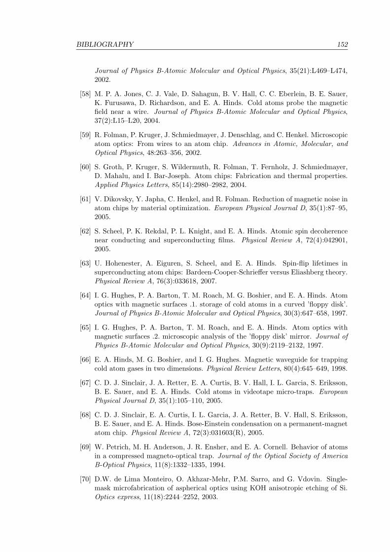
BIBLIOGRAPHY 152
Journal of Physics B-Atomic Molecular and Optical Physics, 35(21):L469–L474,2002.
[58] M. P. A. Jones, C. J. Vale, D. Sahagun, B. V. Hall, C. C. Eberlein, B. E. Sauer,K. Furusawa, D. Richardson, and E. A. Hinds. Cold atoms probe the magneticfield near a wire. Journal of Physics B-Atomic Molecular and Optical Physics,37(2):L15–L20, 2004.
[59] R. Folman, P. Kruger, J. Schmiedmayer, J. Denschlag, and C. Henkel. Microscopicatom optics: From wires to an atom chip. Advances in Atomic, Molecular, andOptical Physics, 48:263–356, 2002.
[60] S. Groth, P. Kruger, S. Wildermuth, R. Folman, T. Fernholz, J. Schmiedmayer,D. Mahalu, and I. Bar-Joseph. Atom chips: Fabrication and thermal properties.Applied Physics Letters, 85(14):2980–2982, 2004.
[61] V. Dikovsky, Y. Japha, C. Henkel, and R. Folman. Reduction of magnetic noise inatom chips by material optimization. European Physical Journal D, 35(1):87–95,2005.
[62] S. Scheel, P. K. Rekdal, P. L. Knight, and E. A. Hinds. Atomic spin decoherencenear conducting and superconducting films. Physical Review A, 72(4):042901,2005.
[63] U. Hohenester, A. Eiguren, S. Scheel, and E. A. Hinds. Spin-flip lifetimes insuperconducting atom chips: Bardeen-Cooper-Schrie"er versus Eliashberg theory.Physical Review A, 76(3):033618, 2007.
[64] I. G. Hughes, P. A. Barton, T. M. Roach, M. G. Boshier, and E. A. Hinds. Atomoptics with magnetic surfaces .1. storage of cold atoms in a curved ’floppy disk’.Journal of Physics B-Atomic Molecular and Optical Physics, 30(3):647–658, 1997.
[65] I. G. Hughes, P. A. Barton, T. M. Roach, and E. A. Hinds. Atom optics withmagnetic surfaces .2. microscopic analysis of the ’floppy disk’ mirror. Journal ofPhysics B-Atomic Molecular and Optical Physics, 30(9):2119–2132, 1997.
[66] E. A. Hinds, M. G. Boshier, and I. G. Hughes. Magnetic waveguide for trappingcold atom gases in two dimensions. Physical Review Letters, 80(4):645–649, 1998.
[67] C. D. J. Sinclair, J. A. Retter, E. A. Curtis, B. V. Hall, I. L. Garcia, S. Eriksson,B. E. Sauer, and E. A. Hinds. Cold atoms in videotape micro-traps. EuropeanPhysical Journal D, 35(1):105–110, 2005.
[68] C. D. J. Sinclair, E. A. Curtis, I. L. Garcia, J. A. Retter, B. V. Hall, S. Eriksson,B. E. Sauer, and E. A. Hinds. Bose-Einstein condensation on a permanent-magnetatom chip. Physical Review A, 72(3):031603(R), 2005.
[69] W. Petrich, M. H. Anderson, J. R. Ensher, and E. A. Cornell. Behavior of atomsin a compressed magneto-optical trap. Journal of the Optical Society of AmericaB-Optical Physics, 11(8):1332–1335, 1994.
[70] D.W. de Lima Monteiro, O. Akhzar-Mehr, P.M. Sarro, and G. Vdovin. Single-mask microfabrication of aspherical optics using KOH anisotropic etching of Si.Optics express, 11(18):2244–2252, 2003.
BIBLIOGRAPHY 153
[71] K. I. Lee, J. A. Kim, H. R. Noh, and W. Jhe. Single-beam atom trap in apyramidal and conical hollow mirror. Optics Letters, 21(15):1177–1179, 1996.
[72] M. Trupke, F. Ramirez-Martinez, E. A. Curtis, J. P. Ashmore, S. Eriksson, E. A.Hinds, Z. Moktadir, C. Gollasch, M. Kraft, G. V. Prakash, and J. J. Baumberg.Pyramidal micromirrors for microsystems and atom chips. Applied Physics Let-ters, 88(7):071116, 2006.
[73] M. Mansuripur. The physical principles of magneto-optical recording. CambridgeUniversity Press, Cambridge, 1995.
[74] C. J. Lin, G. L. Gorman, C. H. Lee, R. F. C. Farrow, E. E. Marinero, H. V.Do, H. Notarys, and C. J. Chien. Magnetic and structural properties of Co/Ptmultilayers. Journal of Magnetism and Magnetic Materials, 93:194–206, 1991.
[75] Jocelyn Anna Retter. Cold Atom Microtraps above a Video Tape Surface. PhDthesis, University of Sussex, 2002.
[76] S. Eriksson, F. Ramirez-Martinez, E. Curtis, B. Sauer, P. Nutter, E. Hill, andE. Hinds. Micron-sized atom traps made from magneto-optical thin films. Appl.Phys. B, 79:811, 2004.
[77] H. J. Metcalf and P. Van der Straten. Laser Cooling and Trapping. Springer-Verlag, New York, 1999.
[78] K. Lindquist, M. Stephens, and C. Wieman. Experimental and theoretical studyof the vapor-cell Zeeman optical trap. Physical Review A, 46(7):4082–4090, 1992.
[79] A. M. Steane, M. Chowdhury, and C. J. Foot. Radiation force in the magneto-optical trap. Journal of the Optical Society of America B-Optical Physics,9(12):2142–2158, 1992.
[80] J. A. Kim, K. I. Lee, H. R. Noh, W. Jhe, and M. Ohtsu. Atom trap in an axiconmirror. Optics Letters, 22(2):117–119, 1997.
[81] Young-Tak Chough and Wonho Jhe. A computational analysis of an axiconmagneto-optical trap. Journal of the Physical Society of Japan, 69(5):1366–1373,May 2000.
[82] E. Arimondo, M. Inguscio, and P. Violino. Experimental determinations ofhyperfine-structure in alkali atoms. Reviews of Modern Physics, 49(1):31–75, 1977.
[83] D. Sesko, T. Walker, C. Monroe, A. Gallagher, and C. Wieman. Collisional lossesfrom a light-force atom trap. Physical Review Letters, 63(9):961–964, 1989.
[84] Frederick Reif. Fundamentals of statistical and thermal physics. McGraw-Hillseries in fundamentals of physics. McGraw-Hill, New York, 1965.
[85] U. D. Rapol, A. Wasan, and V. Natarajan. Loading of a Rb magneto-optic trapfrom a getter source. Physical Review A, 64(2):023402, 2001.
[86] J. A. Kim, K. I. Lee, H. Nha, H. R. Noh, and W. Jhe. Simple atom trap in aconical hollow mirror: Numerical analysis. Journal of the Korean Physical Society,30(2):387–390, 1997.
BIBLIOGRAPHY 154
[87] K. H. Kim, K. I. Lee, H. R. Noh, W. Jhe, N. Kwon, and M. Ohtsu. Cold atomicbeam produced by a conical mirror funnel. Physical Review A, 64(1):013402, 2001.
[88] H. R. Noh and W. Jhe. Atom optics with hollow optical systems. Physics Reports-Review Section of Physics Letters, 372(3):269–317, 2002.
[89] J. M. Kohel, J. Ramirez-Serrano, R. J. Thompson, and L. Maleki. Generation ofan intense cold-atom beam from a pyramidal magneto-optical trap: experimentand simulation. Journal of the Optical Society of America B-Optical Physics,20(6):1161–1168, 2003.
[90] A. S. Mellish and A. C. Wilson. A simple laser cooling and trapping apparatus forundergraduate laboratories. American Journal of Physics, 70(9):965–971, 2002.
[91] W. A. Nierenberg. The measurement of the nuclear spins and static moments ofradioactive isotopes. Annu. Rev. Nucl. Sci., 7:349–406, 1957.
[92] G. Breit and I. I. Rabi. Measurement of nuclear spin. Physical Review, 38(11):2082,1931.
[93] D. M. Brink and C. V. Sukumar. Majorana spin-flip transitions in a magnetictrap. Physical Review A, 74(3):035401, 2006.
[94] W. Demtroder. Laser spectroscopy : basic concepts and instrumentation. Ad-vanced texts in physics. Springer, New York, 3rd edition, 2003.
[95] Daniel A. Steck. Rubidium 87 D Line Data. The current version of this documentis available at http://steck.us/alkalidata, October 2003.
[96] A. S. Arnold, J. S. Wilson, and M. G. Boshier. A simple extended-cavity diodelaser. Review of Scientific Instruments, 69(3):1236–1239, 1998.
[97] C. P. Pearman, C. S. Adams, S. G. Cox, P. F. Gri!n, D. A. Smith, and I. G.Hughes. Polarization spectroscopy of a closed atomic transition: applicationsto laser frequency locking. Journal of Physics B-Atomic Molecular and OpticalPhysics, 35(24):5141–5151, 2002.
[98] Sacher Lasertechnik Group. Technical documentation: Spectroscopy with diodelasers. http://data.sacher-laser.com/techdocs/dlspec.pdf.
[99] K. L. Corwin, Z. T. Lu, C. F. Hand, R. J. Epstein, and C. E. Wieman. Frequency-stabilized diode laser with the Zeeman shift in an atomic vapor. Applied Optics,37(15):3295–3298, 1998.
[100] Bahaa E. A. Saleh and Malvin Carl Teich. Fundamentals of photonics. Wiley,1991.
[101] David W. Allan. Time and frequency (time-domain) characterization, estima-tion, and prediction of precision clocks and oscillators. IEEE Transactions onUltrasonics, Ferroelectrics, and Frequency Control., URC-34(6):647–654, 1967.
[102] Marvin J. Weber. Handbook of Optical Materials. CRC Press, 2003.
BIBLIOGRAPHY 155
[103] C. G. Townsend, N. H. Edwards, C. J. Cooper, K. P. Zetie, C. J. Foot, A. M.Steane, P. Szriftgiser, H. Perrin, and J. Dalibard. Phase-space density in themagnetooptical trap. Physical Review A, 52(2):1423–1440, 1995.
[104] E. Bassous. Fabrication of novel 3-dimensional microstructures by anisotropicetching of (100) and (110) silicon. IEEE Transactions on Electron Devices,25(10):1178–1185, 1978.
[105] G. B. Friedmann and H. S. Sandhu. Phase changes on reflection from a metallicsurface. American Journal of Physics, 56:270–273, 1988.
[106] L. B. Wol". Polarization-based material classification from specular reflection.IEEE Transactions on Pattern Analysis and Machine Intelligence, 12(11):1059–1071, 1990.
[107] H. Chen and L. B. Wol". Polarization phase-based method for material classifica-tion in computer vision. International Journal of Computer Vision, 28(1):73–83,1998.
[108] Robert Siegel and John R. Howell. Thermal radiation heat transfer. Taylor &Francis, New York, 4th edition, 2001.
[109] G. Lewis, Z. Moktadir, C. Gollasch, M. Kraft, S. Pollock, F. Ramirez-Martinez,J. P. Ashmore, A. Laliotis, M. Trupke, and E. A. Hinds. Fabrication of magneto-optical atom traps on a chip. arXiv:0804.4593v1 [physics.atom-ph], 2008.
[110] T. A. Delchar. Vacuum physics and techniques. Number 6 in Physics and itsapplications. Chapman & Hall, London, 1993.
[111] C. Rouki, L. Westerberg, and Chicsi Dev Grp. Ultra-high vacuum compatibilitymeasurements of materials for the CHICSi detector system. Physica Scripta,T104:107–108, 2003.
[112] L. Westerberg, V. Avdeichikov, L. Carlen, P. Golubev, B. Jakobsson, C. Rouki,A. Siwek, E. J. van Veldhuizen, and H. J. Whitlow. CHICSi - a compact ultra-highvacuum compatible detector system for nuclear reaction experiments at storagerings. I. General structure, mechanics and UHV compatibility. Nuclear Instru-ments & Methods in Physics Research Section a-Accelerators Spectrometers De-tectors and Associated Equipment, 500(1-3):84–95, 2003.
[113] FR4 Data Sheet. http://www.p-m-services.co.uk/fr4 data sheet.htm.
[114] H. S. Nalwa. Handbook of thin film materials: Nanomaterials and Magnetic ThinFilms., volume 5. Academic Press, New York, 2002.
[115] S. Uba, L. Uba, A. N. Yaresko, A. Y. Perlov, V. N. Antonov, and R. Gontarz.Optical and magneto-optical properties of Co/Pt multilayers. Physical Review B,53(10):6526–6535, 1996.
[116] R. A. Fry, L. H. Bennett, E. Della Torre, and R. F. C. Farrow. Magneto-optical be-havior in Co/Pt ultrathin film multilayers. Journal of Applied Physics, 87(9):5765–5767, 2000.
BIBLIOGRAPHY 156
[117] G. N. Phillips, K. O’Grady, Q. Meng, and J. C. Lodder. Domain structure andmagnetisation processes in magneto-optic Co/Pt thin films. IEEE Transactionson Magnetics, 32(5):4070–4072, 1996.
[118] G. N. Phillips, K. OGrady, and J. C. Lodder. Magnetization reversal at ele-vated temperatures in Co/Pt multilayer thin films. Journal of Physics D: AppliedPhysics, 34:29602971, 2001.
[119] Y. C. Cho, S. B. Choe, and S. C. Shin. Magnetic field dependence of magnetizationreversal behavior in Co/Pt multilayers. Journal of Applied Physics, 90(3):1419–1421, 2001.
[120] M. Kisielewski, A. Maziewski, M. Tekielak, J. Ferre, S. Lemerle, V. Mathet,and C. Chappert. Magnetic anisotropy and magnetization reversal processes inPt/Co/Pt films. Journal of Magnetism and Magnetic Materials, 260(1-2):231–243,2003.
[121] Ch. Kittel. Introduction to Solid State Physics. John Wiley and Sons, New York,1971.
[122] Z. Q. Qiu and S. D. Bader. Surface magneto-optic kerr e"ect. Review of ScientificInstruments, 71(3):1243–1255, 2000.
[123] Z. Q. Qiu and S. D. Bader. Surface magneto-optic kerr e"ect (SMOKE). Journalof Magnetism and Magnetic Materials, 200(1-3):664–678, 1999.
[124] M. Mansuripur, G. A. N. Connell, and J. W. Goodman. Laser-induced localheating of multilayers. Applied Optics, 21(6):1106–1114, 1982.
[125] M. Mansuripur and G. A. N. Connell. Laser-induced local heating of movingmultilayer media. Applied Optics, 22(5):666–670, 1983.
[126] M. Mansuripur and G. A. N. Connell. Thermal aspects of magneto-optical record-ing. Journal of Applied Physics, 54(9):4794–4798, 1983.
[127] M. Mansuripur and G. A. N. Connell. Energetics of domain formation in thermo-magnetic recording. Journal of Applied Physics, 55(8):3049–3055, 1984.
[128] M. Mansuripur and T. W. Mcdaniel. Magnetization reversal dynamics in magneto-optic media. Journal of Applied Physics, 63(8):3831–3834, 1988.
[129] B. E. Bernacki and M. Mansuripur. Characterization of magnetooptical record-ing media in terms of domain boundary jaggedness. Journal of Applied Physics,69(8):4960–4962, 1991.
[130] D. W. Sesko, T. G. Walker, and C. E. Wieman. Behavior of neutral atoms ina spontaneous force trap. Journal of the Optical Society of America B-OpticalPhysics, 8(5):946–958, 1991.
157
Appendix A
Pumping down procedure
Initially, the chamber is pumped through the angle valve by a turbo molecular pump forat least one hour before attempting to turn on the ion pump. After this initial pumpingstage, the ion pump is switched on and an initial reading in the middle 10"4 mbar regionis normally obtained. At this point and provided that the pressure is in this range, theion pump can be left pumping for a few hours.
When the pressure reading in the ion pump controller is in the low 10"5 mbar orhigh 10"6 mbar region, it is possible to begin outgassing the contents of the chamber.These contents are a pair of anti-Helmholtz coils which is described in section 3.4.1,the rubidium dispenser described in section 3.1.2, and the atom chip assembly that isfully described in section 5.3.1. We begin by heating up the coil pair by running currentthrough them and monitoring the corresponding temperature variation by recording thechange in the coil resistance. As the coil temperature increases, so does the outgassingrate and this is reflected in the chamber pressure. However, once the coil temperaturehas stabilised at a certain value, the outgassing rate gradually decreases and the pressurecomes back down. The current supplied to these coils is raised in small amounts, alwayskeeping the pressure in the chamber below 10"4 mbar.
Once the coil temperature has been stabilised at around 100 !C and the pressurehas dropped below 10"6 mbar, it is possible to begin outgassing the rubidium dispenser.Although the nominal activation current of these dispensers is as high as 4.5 A, imme-diately after loading a dispenser into the vacuum chamber, currents as low as a fewhundreds of mA are enough to expel a large amount of material. We have found thatduring the initial dispenser outgassing stages, the current needs to be raised in steps assmall as 250 mA. Each one of these steps pushes the pressure briefly up to the 10"4 mbarrange, before the turbo pump brings the pressure back down into the 10"7 mbar range ina few minutes. This procedure is repeated until a current of up to 6 A has been reached.Once the 4.5 A activation threshold has been crossed, a laser beam tuned to one of therubidium transitions is sent into the vacuum chamber. The appearance of fluorescencein the path of this resonant beam indicates the presence of Rb in the chamber and, inconsequence, the correct operation of the dispenser. At this point, the current suppliescan be turned o" and both vacuum pumps are left pumping for several hours. Next,the angle valve is closed and from this point onwards the ion pump alone will su!ce to

A. Pumping down procedure 158
take the pressure below 10"8 mbar in a few days and below 10"9 mbar in less than aweek.
When the atom chip assembly, which is described in sections 3.1.3 and 5.3.1, wereincluded in the experimental apparatus, we found it necessary to add a full chamberbake-out stage to the pumping down procedure. We do this with the aim of keepingthe pumping-down period as short as possible. In this stage, three heaters are woundaround the vacuum chamber, especially in the top 8” port area. This is because all theelements of our experiments are attached to the flange that seals that port. This flangeis then kept at a temperature between 100 !C and 120 !C for two or three days, whileboth the turbo pump and the ion pump are kept working. Following this procedure, apressure below 10"9 mbar can be achieved in approximately one week.
159
Appendix B
The rate of losses to a wall
The loss rate can be estimated by considering the number of atoms per unit timecolliding with a surface located at a distance d from the trap centre. The atom flux canbe simply written as %0 = 1
4nv and, as we are interested in clouds containing ! 105
atoms, it is justified to consider an atom density following a gaussian distribution aroundthe trap centre. Hence, the total number of atoms striking the surface per unit time isestimated by summing this flux over the entire wall surface, L =
:%0dA,
L =14v
+ (
"(
+ (
"(n0e
" 12 ( x
!x)2e
" 12 ( y
!y)2
e"12 ( z
!z)2dxdz (B.1)
This is then evaluated at y = d to give:
L =&%2vn0,
2e"12( d
! )2
(B.2)
Here we have considered that the cloud extent in each direction is determined by themagnetic field gradient and , = ,x = ,y =
%2,z.
The maximum number of atoms recorded in the loss rate measurements is of theorder of 105 atoms. This suggest that in these extreme cases we are operating in thefrontier between the temperature limited and the multiple scattering regimes, althoughin general the number of atoms was below this limit [103]. Consequently, our modelmust be developed for either of the two possible regimes. Firstly, in the temperaturelimited regime, as more atoms are added to the trap, the cloud radius remains constantand the density is determined by the total number of trapped atoms. However, theextent of the cloud is restricted by the proximity of the wall. Consequently, the cloudpopulation N can be calculated by integrating the gaussian atom distribution with therestriction imposed by the wall:
N =+ (
"(
+ d
"(
+ (
"(n0e
" 12 ( x
!x)2e
" 12 ( y
!y)2
e"12 ( z
!z)2dxdydz
This leads toN = 2&3/2,3n0
-1 + Erf(
d%2,
).
(B.3)
B. The rate of losses to a wall 160
where Erf(x) denotes the Gauss error function
Erf(x) =2%&
+ x
0e"t2dt
This result can be used to express the cloud density in terms of the number of atomscollected in the trap, which then can be substituted into equation B.2. Furthermore,the wall loss rate results to be proportional to the number of atoms in the trap and wecan write LTL = (TLN , where
(TL =ve"
12( d
! )2
%8&,
41 + Erf( d%
2()5 (B.4)
is the wall contribution to the loss rate in the temperature limited regime (TL). Theoverall loss rate can then be expressed as ( = #nRb + (B + (TL, which is the parameterthat we have determined experimentally.
In the multiple scattering regime, the cloud density is limited by the reabsorptionof photons within the trap. The cloud radius is then determined by the total number oftrapped atoms and, as it has been pointed out in [130], in this regime the cloud beginsto di"er from a gaussian distribution. However, the clouds generated in our experimentsare not far from the border between the two regimes and for this estimation we assumethat the distribution is still very close to a gaussian, which is consistent with what wehave seen in our experiments. Then, the number of atoms collected in the trap is givenby
N = (2&)3/2n0,3 (B.5)
In order to determine the actual density at which the atom cloud saturates, we con-sidered a cold atom cloud in a MOT generated far from the wall. In this situation,
nMS =N
4&3/2,3(B.6)
and N and , are taken to be typical values for a large cloud.This density can now be utilised to express the cloud radius in terms of the number
of atoms in the trap and the result can be substituted in equation B.2,
LMS =21/6
4vN2/3n1/3
MS exp
8"21/3&d2n2/3
MS
N2/3
9(B.7)
In contrast to what was found for the temperature limited regime, LMS is a complicatedfunction of the number of atoms collected in the trap. Therefore, to see how this esti-mation compares with the results of our experiments, we need to insert this expressionin the MOT filling equation considering the losses to the wall separately,
dN
dt= R" (#nRb + (B) N " LMS (B.8)
Considering the steady state situation dNdt = 0, we can write
R" (#nRb + (B + (MS) NS = 0 (B.9)
with (MS = NS"1LMS. This equation can be solved numerically for NS and the solution
can be used in B.7 to express the dependency of the MOT loss rate on the distance tothe surface in the multiple scattering regime.

B. The rate of losses to a wall 161
We have shown how the interaction between the cold atom cloud and a room temper-ature surface is expected to influence the trap loss rate. In our analysis, a distinction wasmade between the temperature limited (TL) and the multiple scattering (MS) regimes.In order to demonstrate how these models recreate the real situation, in figure 4.19 wehave included a pair of curves corresponding to each of these models. The values of theparameters that were utilised for generating these curves are typical of our experiments,but do not represent a fitting of the model to the experimental data.
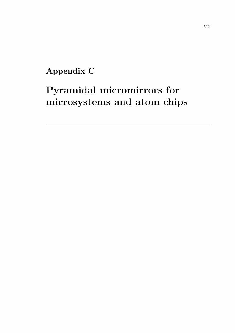
162
Appendix C
Pyramidal micromirrors formicrosystems and atom chips
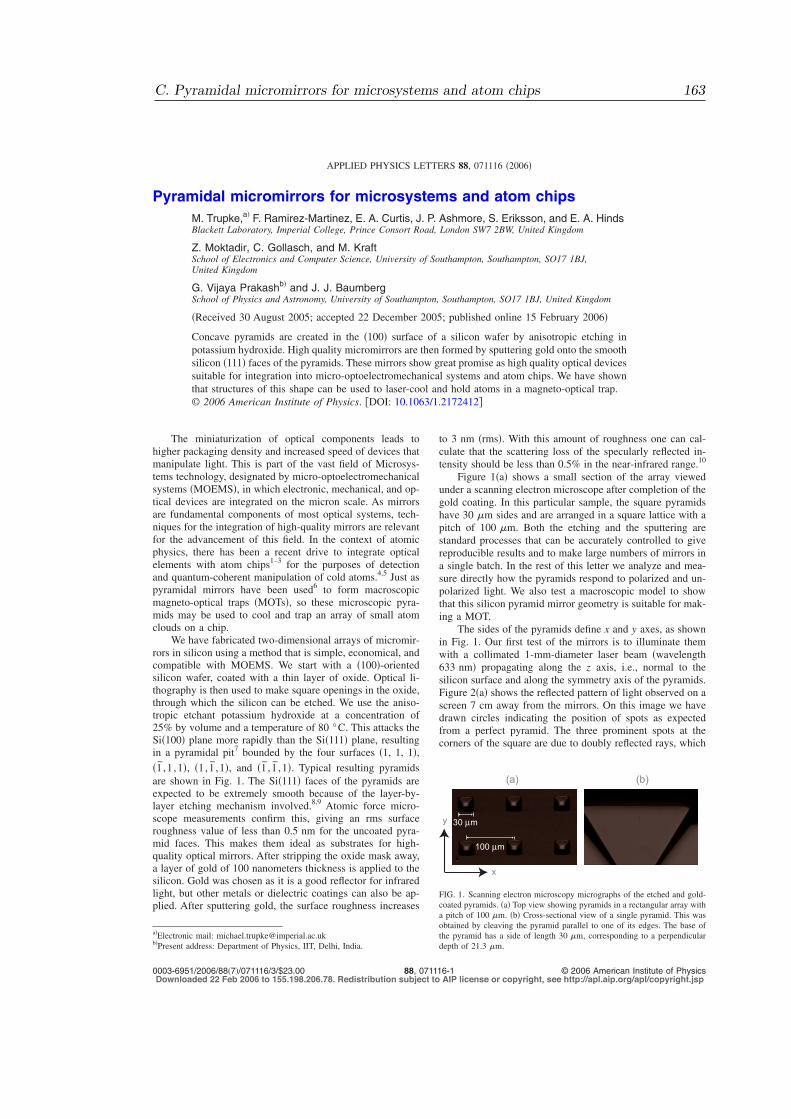
Pyramidal micromirrors for microsystems and atom chipsM. Trupke,a! F. Ramirez-Martinez, E. A. Curtis, J. P. Ashmore, S. Eriksson, and E. A. HindsBlackett Laboratory, Imperial College, Prince Consort Road, London SW7 2BW, United Kingdom
Z. Moktadir, C. Gollasch, and M. KraftSchool of Electronics and Computer Science, University of Southampton, Southampton, SO17 1BJ,United Kingdom
G. Vijaya Prakashb! and J. J. BaumbergSchool of Physics and Astronomy, University of Southampton, Southampton, SO17 1BJ, United Kingdom
!Received 30 August 2005; accepted 22 December 2005; published online 15 February 2006"
Concave pyramids are created in the !100" surface of a silicon wafer by anisotropic etching inpotassium hydroxide. High quality micromirrors are then formed by sputtering gold onto the smoothsilicon !111" faces of the pyramids. These mirrors show great promise as high quality optical devicessuitable for integration into micro-optoelectromechanical systems and atom chips. We have shownthat structures of this shape can be used to laser-cool and hold atoms in a magneto-optical trap.© 2006 American Institute of Physics. #DOI: 10.1063/1.2172412$
The miniaturization of optical components leads tohigher packaging density and increased speed of devices thatmanipulate light. This is part of the vast field of Microsys-tems technology, designated by micro-optoelectromechanicalsystems !MOEMS", in which electronic, mechanical, and op-tical devices are integrated on the micron scale. As mirrorsare fundamental components of most optical systems, tech-niques for the integration of high-quality mirrors are relevantfor the advancement of this field. In the context of atomicphysics, there has been a recent drive to integrate opticalelements with atom chips1–3 for the purposes of detectionand quantum-coherent manipulation of cold atoms.4,5 Just aspyramidal mirrors have been used6 to form macroscopicmagneto-optical traps !MOTs", so these microscopic pyra-mids may be used to cool and trap an array of small atomclouds on a chip.
We have fabricated two-dimensional arrays of micromir-rors in silicon using a method that is simple, economical, andcompatible with MOEMS. We start with a !100"-orientedsilicon wafer, coated with a thin layer of oxide. Optical li-thography is then used to make square openings in the oxide,through which the silicon can be etched. We use the aniso-tropic etchant potassium hydroxide at a concentration of25% by volume and a temperature of 80 °C. This attacks theSi!100" plane more rapidly than the Si!111" plane, resultingin a pyramidal pit7 bounded by the four surfaces !1, 1, 1",!1 ,1 ,1", !1, 1 ,1", and !1 , 1 ,1". Typical resulting pyramidsare shown in Fig. 1. The Si!111" faces of the pyramids areexpected to be extremely smooth because of the layer-by-layer etching mechanism involved.8,9 Atomic force micro-scope measurements confirm this, giving an rms surfaceroughness value of less than 0.5 nm for the uncoated pyra-mid faces. This makes them ideal as substrates for high-quality optical mirrors. After stripping the oxide mask away,a layer of gold of 100 nanometers thickness is applied to thesilicon. Gold was chosen as it is a good reflector for infraredlight, but other metals or dielectric coatings can also be ap-plied. After sputtering gold, the surface roughness increases
to 3 nm !rms". With this amount of roughness one can cal-culate that the scattering loss of the specularly reflected in-tensity should be less than 0.5% in the near-infrared range.10
Figure 1!a" shows a small section of the array viewedunder a scanning electron microscope after completion of thegold coating. In this particular sample, the square pyramidshave 30 !m sides and are arranged in a square lattice with apitch of 100 !m. Both the etching and the sputtering arestandard processes that can be accurately controlled to givereproducible results and to make large numbers of mirrors ina single batch. In the rest of this letter we analyze and mea-sure directly how the pyramids respond to polarized and un-polarized light. We also test a macroscopic model to showthat this silicon pyramid mirror geometry is suitable for mak-ing a MOT.
The sides of the pyramids define x and y axes, as shownin Fig. 1. Our first test of the mirrors is to illuminate themwith a collimated 1-mm-diameter laser beam !wavelength633 nm" propagating along the z axis, i.e., normal to thesilicon surface and along the symmetry axis of the pyramids.Figure 2!a" shows the reflected pattern of light observed on ascreen 7 cm away from the mirrors. On this image we havedrawn circles indicating the position of spots as expectedfrom a perfect pyramid. The three prominent spots at thecorners of the square are due to doubly reflected rays, which
a"Electronic mail: [email protected]"Present address: Department of Physics, IIT, Delhi, India.
(b)(a)
y
x
30 µm
100 µm
FIG. 1. Scanning electron microscopy micrographs of the etched and gold-coated pyramids. !a" Top view showing pyramids in a rectangular array witha pitch of 100 !m. !b" Cross-sectional view of a single pyramid. This wasobtained by cleaving the pyramid parallel to one of its edges. The base ofthe pyramid has a side of length 30 !m, corresponding to a perpendiculardepth of 21.3 !m.
APPLIED PHYSICS LETTERS 88, 071116 !2006"
0003-6951/2006/88"7!/071116/3/$23.00 © 2006 American Institute of Physics88, 071116-1Downloaded 22 Feb 2006 to 155.198.206.78. Redistribution subject to AIP license or copyright, see http://apl.aip.org/apl/copyright.jsp
C. Pyramidal micromirrors for microsystems and atom chips 163
we classify as type !1". These reflect from opposite faces ofthe pyramid, as illustrated by the solid line in Fig. 3!a". Thereshould be a fourth spot at the bottom of the photographs, butthis is blocked by a mount holding the beamsplitter throughwhich the array is illuminated.
If the angle between opposite mirrors is ", the type !1"beams make an angle of !#!2"" with the z axis. From theangles measured, we find that "= !70.6±0.7"°, in agreementwith the expected angle between opposing faces ofarccos!1/3"=70.5°.
When the incident ray is close to the apex of the pyramid!within 1.6 !m for a pyramid of 30 !m base length", it isreflected twice by the first mirror, as illustrated by the dashedline in Fig. 3!a". These rays, which we call type !2", shouldproduce secondary spots just inside the type !1" spots. How-ever, the power in the type !2" reflected beams is expected tobe 100 times smaller because of the small area from whichthey originate, as shown in Fig. 3!b". Consequently, it is notpossible to identify the type !2" beams clearly against thediffracted wings of the type !1" beams. Furthermore, there isa background of light along the x and y axes caused byreflection from rounded edges on the entrance aperture of thepyramid, which can be seen in Fig. 1!b".
If a ray is incident near one of the corners of the pyra-mid, the first reflection sends it off towards the opposite mir-ror, but it is intercepted and deflected by the adjacent mirrorbefore the opposite mirror sends it out of the pyramid as atype !3" ray. These rays make an angle of 31.5° with the z
axis and form double spots at azimuthal angles of 36.9°,53.1°, etc. as shown in Fig. 2!a". These spots are less distinctthan those of type !1" because the corners of the pyramid arerounded, a feature that does not affect the type !1" rays.Figure 2!b" shows the same photographed reflection pattern,but here the superimposed circles indicate the expected po-sition and magnitude of spots reflected from a pyramid withrounded corners. The roundness is included in the ray-tracingmodel by four additional surfaces at each corner. These areshaped to form approximate cone sections with radii of2.5 !m at the base and 0.825 !m at the apex of the pyramid.The reflection pattern predicted for this modified shapematches many of the features of the photographed intensitydistribution more closely.
The three types of ray described earlier also present dif-ferent characteristics when observed using polarized light.For our observations, we use light which is polarized parallelto the x axis. Reflections of types !1" and !2" leave the linearpolarization of the light unchanged in the x-y plane. The type!3" reflections produce rotations of ±53° or ±78° about the zaxis, depending on whether the pyramid face on which thefirst bounce occurs is parallel to the polarization of incomingbeam. The rotations are caused by the obliquity of the secondand third bounces of the type !3" reflections.11 This is inves-tigated in our second test of the mirrors, in which we exam-ine them with white light under an optical microscope, illu-minating them once again along the z axis. Figure 4!a" showsthe image calculated by ray tracing for unpolarized light withthe microscope focussed in the plane of the apex of a perfectpyramid. In this figure most of the area is bright. In Fig. 4!b"we show the expected image for linearly polarized light,viewed through a parallel analyser, which suppresses thetype !3" contribution. This leads to a reduction in the inten-sity of reflections from the corner region. In Fig. 4!c", theanalyzer is crossed with the polarizer and only type !3" rayscontribute, making the corner region bright. The intensitypatterns observed in the laboratory are shown in Figs.4!d"–4!f". They correspond closely to the calculated distribu-tions, indicating that the pyramid reflects light as expected.
Our immediate application for these structures is to buildan array of small magneto-optical traps, integrated into anatom chip in a single additional etching step. As in a 90°pyramid MOT,6 lateral confinement is given by the first re-
FIG. 2. !Color online" Measured intensity distribution of reflected light, at adistance of 7 cm from the array of pyramids, when it is illuminated atnormal incidence. A central bright spot, which is caused by reflection fromthe region between pyramids, was blocked to improve the visibility of lightreflected from the pyramids. The circles in !a" show the reflection patternexpected for a perfect pyramid, while the circles in !b" indicate the calcu-lated reflection pattern for a pyramid with rounded corners. Size indicatesexpected relative intensity.
FIG. 3. !Color online" !a" Cross section in the x-z plane through a pyramid,showing type !1" and !2" trajectories. These involve reflections from mirrorson opposite sides of the pyramid. !b" View of the entrance aperture of thepyramid, showing the regions that produce type !1", !2", and !3" rays.
FIG. 4. Views of the vertex pyramidal mirror under an optical microscope at100$ magnification. Top row: Raytracing simulation. Bottom row: Photo-graphs. !a" and !d" without polarizers; !b" and !e" parallel polarizer andanalyzer; !c" and !f" crossed polarizer and analyzer.
071116-2 Trupke et al. Appl. Phys. Lett. 88, 071116 "2006!
Downloaded 22 Feb 2006 to 155.198.206.78. Redistribution subject to AIP license or copyright, see http://apl.aip.org/apl/copyright.jsp
C. Pyramidal micromirrors for microsystems and atom chips 164
flections of the type !1" beams, while the vertical trappingforces arise from the input beam and the second reflectionsof the type !1" beams. In the present pyramid the beams arenot orthogonal and there are additional rays, which couldalso disturb the balance of forces in the trap. To test whetherit is nonetheless possible to trap atoms in such a pyramid, weconstructed a macroscopic glass model with a base length of16.3 mm, coated with aluminium and a protective layer ofSiO2. Figure 5 shows the fluorescence image from a cloud ofatoms trapped in this pyramid MOT, together with two re-flections of the cloud. There are also reflections from the topface of the pyramid and from the edges. In order to assist theeye, we superimpose the entrance aperture of the pyramid asa solid line and we show the edges dashed. We have alsobuilt and tested a 90° pyramid MOT of similar volume andwith the same coating, and find that there is no significantdifference in the number of trapped atoms or in the stabilityof the MOT.
In the microscopic version, we anticipate using pyramidswith a 200 !m base and will supply the required magneticquadrupole field using existing microfabrication methods1,12
to produce small current loops around each pyramid. Weestimate that such a MOT can collect as many as 1000 atomsor as few as 1, according to the choice of operating param-eters. Compared with other methods of creating arrays ofmicroscopic traps on a chip,13,14 this relies on a simple fab-rication method and requires only a single input laser beamto give all the necessary trapping beams. It has been shownthat Bose-Einstein condensation can be achieved on atomchips, both with current-carrying wire traps15 and with per-manent magnet traps.16 Consequently it may be possible tocreate an array of condensates loaded from these MOTs. Al-ternatively, if there is just one atom per site, the array would
have possible applications in quantum informationprocessing.4
Further potential applications for the pyramids are in theareas of photonics and telecommunications. For example, byfilling the pits with ferroelectric material or liquid crystalsand applying an electric field, it may be possible to use thepyramids as fast optical switches.
In summary, we have designed, fabricated and character-ized a new type of micromirror, produced by anisotropicetching through square apertures on a silicon single crystal.As an elementary component for optics, the micromirror hasa variety of possible applications in MOEMS devices. Wehave demonstrated that it is possible to form a magneto-optical trap with this mirror geometry, making these pyra-mids very promising for creating arrays of microscopic trapson atom chips. Detailed experiments and further theoreticalanalysis are currently under way to develop theseapplications.
The authors acknowledge support from the UK EPSRCBasic Technology, QIPIRC, and Physics programmes andfrom the FASTNET and Atom Chips networks of the Euro-pean Commission.
1R. Folman, P. Krueger, J. Schmiedmayer, J. Denschlag, and C. Henkel,Adv. At. Mol. Phys. 48, 263 !2002".
2S. Eriksson, M. Trupke, H. F. Powell, D. Sahagun, C. D. J. Sinclair, E. A.Curtis, B. E. Sauer, E. A. Hinds, Z. Moktadir, C. O. Gollasch, and M.Kraft, Eur. Phys. J. D 35, 135 !2005".
3M. Trupke, E. A. Hinds, S. Eriksson, E. A. Curtis, Z. M. E. Kukarenka,and M. Kraft, Appl. Phys. Lett. 87, 211106 !2005".
4S. Scheel, J. Pachos, and P. L. Hinds, and E. A. Knight, Quantum Coher-ence, Lecture Notes in Physics Vol. 689 !Springer, Berlin, 2006", pp. 47–80.
5P. Horak, B. Klappauf, A. Haase, R. Folman, J. Schmiedmayer, P.Domokos, and E. A. Hinds, Phys. Rev. A 67, 043806 !2003".
6K. Lee, J. Kim, H. Noh, and W. Jhe, Opt. Lett. 21, 1177 !1996".7R. Brendel, in Proceedings of the 14th European Photovoltaic Solar En-ergy Conference, edited by H. A. Ossenbrink, P. Helm, and H. Ehmann!Stephens, Bedford, 1997", p. 1354.
8Z. Moktadir and H. Camon, Modell. Simul. Mater. Sci. Eng. 5, 481!1997".
9K. Sato, M. Shikida, T. Yamashiro, M. Tsunekawa, and S. Ito, Sens. Ac-tuators, A A73, 122 !1999".
10P. Beckmann and A. Spizzichino, The Scattering of ElectromagneticWaves from Rough Surfaces !Pergamon, New York, 1963".
11B. A. E. Saleh and M. C. Teich, Fundamentals of Photonics !Wiley, NewYork, 1991".
12S. Eriksson, F. Ramirez-Martinez, E. Curtis, B. Sauer, P. Nutter, E. Hill,and E. Hinds, Appl. Phys. B B79, 811 !2004".
13A. Grabowski and T. Pfau, Eur. Phys. J. D 22, 347 !2003".14E. Hinds, in Atomic Physics 17, AIP Conference Proceedings Vol. 551
edited by E. Arimondo, P. D. Natale, and M. Inguscio !AIP, New York,2001", pp. 405–413.
15H. Ott, J. Fortagh, G. Schlotterbeck, A. Grossmann, and C. Zimmermann,Phys. Rev. Lett. 87, 230401 !2001".
16C. D. J. Sinclair, E. A. Curtis, I. Llorente-Garcia, J. A. Retter, B. V. Hall,S. Eriksson, B. E. Sauer, and E. A. Hinds, Phys. Rev. A 72, 031603!2005".
FIG. 5. !Color online". Fluorescence image of 1.6$108 atoms magneto-optically trapped in a 70.5° pyramid. Two reflections are also visible. The16.3 mm aperture of the pyramid !solid line" and its sloping edges !dashedlines" have been added to guide the eye of the reader. The outline of theincident laser beam is shown dotted. Some light is scattered from the edgesof the pyramid and from the plane outside.
071116-3 Trupke et al. Appl. Phys. Lett. 88, 071116 "2006!
Downloaded 22 Feb 2006 to 155.198.206.78. Redistribution subject to AIP license or copyright, see http://apl.aip.org/apl/copyright.jsp
C. Pyramidal micromirrors for microsystems and atom chips 165
166
Appendix D
Fabrication of magneto-opticalatom traps on a chip
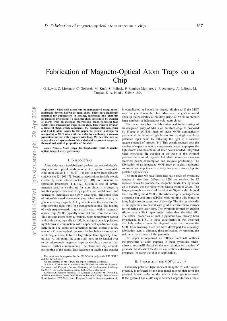
1
Fabrication of Magneto-Optical Atom Traps on aChip
G. Lewis, Z. Moktadir, C. Gollasch, M. Kraft, S. Pollock, F. Ramirez-Martinez, J. P. Ashmore, A. Laliotis, M.Trupke, E. A. Hinds, Fellow, OSA,
Abstract— Ultra-cold atoms can be manipulated using micro-fabricated devices known as atom chips. These have significantpotential for applications in sensing, metrology and quantuminformation processing. To date, the chips are loaded by transferof atoms from an external, macroscopic magneto-optical trap(MOT) into microscopic traps on the chip. This transfer involvesa series of steps, which complicate the experimental procedureand lead to atom losses. In this paper we present a design forintegrating a MOT into a silicon wafer by combining a concavepyramidal mirror with a square wire loop. We describe how anarray of such traps has been fabricated and we present magnetic,thermal and optical properties of the chip.
Index Terms— Atom chips, Electrophoretic resist, Magneto-optical traps, Cavity patterning.
I. INTRODUCTION
Atom chips are microfabricated devices that control electric,magnetic and optical fields in order to trap and manipulatecold atom clouds [1], [2], [3], [4] and to form Bose-Einsteincondensates [5], [6], [7]. Potential applications include atomicclocks [8], atom interferometers [9], [10], and quantum in-formation processors [11], [12]. Silicon is one of severalmaterials used as a substrate for atom chips. It is attractivefor this purpose because its properties are well-known andfabrication techniques are highly developed. The small scaleof microfabricated current-carrying wires makes it easy togenerate strong magnetic field gradients near the surface of thechip, forming tight traps for paramagnetic atoms. The loadingof such magneto-static traps usually starts with a magneto-optical trap (MOT) typically some 3-4 mm from the surface.This collects atoms from a tenuous, room-temperature vapourand cools them, typically to 100 µK, using circularly polarisedlight beams in conjunction with a spherical quadrupole mag-netic field. The atoms are sometimes further cooled to a fewtens of µK using optical molasses, before being captured in aweak magnetic trap to form a large atom cloud, typically 1 mmin size. At this point, the atoms still have to be handed overto the microscopic magnetic traps on the chip, a process thatinvolves further compression of the cloud and very accuratepositioning of the atoms. This sequence of loading and transfer
This work was in supported by the EU SCALA project, the UK EPSRCand the Royal Society.
We are indebted to Mr J. Dyne for expert technical assistance.G. Lewis, Z. Moktadir, C. Gollasch and M. Kraft are with the School of
Electronics and Computer Science, University of Southampton, Southamp-ton,SO17 1BJ, United Kingdom (email:[email protected])
S. Pollock, F. Ramirez-Martinez, J. P. Ashmore, A. Laliotis, M. Trupke & E.A. Hinds are with the Centre for Cold Matter, Imperial College, Prince ConsortRoad, London, SW7 2AZ, United Kingdom (email:[email protected])
is complicated and could be largely eliminated if the MOTwere integrated into the chip. Moreover, integration wouldopen up the possibility of building arrays of MOTs to preparelarge numbers of independent cold atom clouds.
This paper describes the fabrication and initial testing ofan integrated array of MOTs on an atom chip, as proposedby Trupke et al. [13]. Each of these MOTs automaticallyprepares all the required light beams from a single circularlypolarised input beam by reflecting the light in a concavesquare pyramid of mirrors [14]. This greatly reduces both thenumber of expensive optical components needed to prepare thelight beams and the amount of laser power needed. Integratedwires encircling the opening at the base of the pyramidproduce the required magnetic field distributions with modestelectrical power consumption and accurate positioning. Thefabrication of an integrated MOT array on a chip representsan important step towards a truly integrated atom chip forportable applications.
The atom chip we have fabricated has 6 rows of pyramids,ranging in size from 200 µm to 1200 µm, serviced by 12separate wires to produce the magnetic fields. For pyramidsup to 600 µm, the encircling wires have a width of 25 µm. Thelarger pyramids are serviced by wires of 50 µm width. In totalthere are 48 pyramid MOTs. The whole chip is packaged intoa ceramic pin grid array (CPGA) with multiple wire bonds tobring high currents in and out of the chip. The silicon sidewallsof the pyramids are coated with gold to create micro-mirrorsfor reflecting the laser light. The pyramids formed by etchingsilicon have a 70.5o apex angle, rather than the ideal 90o.The optical properties of such a pyramid have already beeninvestigated in [13]. In those experiments it was observedthat light reflected near the diagonal edges can prevent theMOT from working. Here we have developed the necessaryfabrication steps to eliminate these reflections by removing thegold near the corners of the pyramids.
This paper is organised as follows. Section II outlinesthe principles of atom trapping in these pyramidal micro-mirrors, section III describes the microfabrication, section IVpresents initial tests of the device and section V discusses someprospects for using the chip in applications.
II. PRINCIPLE OF THE MOT ON A CHIP
Circularly polarised light, incident along the axis of a squarepyramid, is reflected by the four metal mirrors that form thepyramid. At each reflection the helicity of the light is reversed.If the pyramid has a 90o angle between opposite faces, these
arX
iv:0
804.
4593
v1 [
phys
ics.a
tom
-ph]
29
Apr
200
8D. Fabrication of magneto-optical atom traps on a chip 167
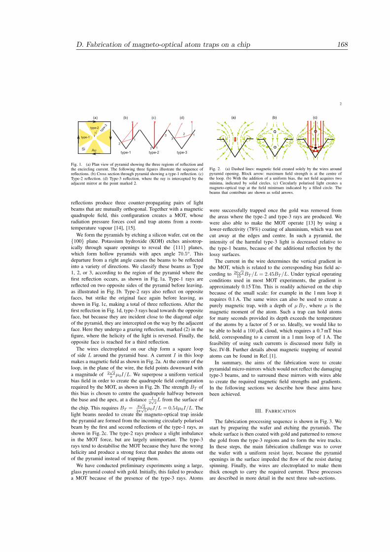
2
2
33
2
2
1
1
1type-1
type-2
type-3
Si Au type-1 type-2 type-3
(a) (b) (c) (d)
Fig. 1. (a) Plan view of pyramid showing the three regions of reflection andthe encircling current. The following three figures illustrate the sequence ofreflections. (b) Cross section through pyramid showing a type-1 reflection. (c)Type-2 reflection. (d) Type-3 reflection, where the ray is intercepted by theadjacent mirror at the point marked 2.
reflections produce three counter-propagating pairs of lightbeams that are mutually orthogonal. Together with a magneticquadrupole field, this configuration creates a MOT, whoseradiation pressure forces cool and trap atoms from a room-temperature vapour [14], [15].
We form the pyramids by etching a silicon wafer, cut on the{100} plane. Potassium hydroxide (KOH) etches anisotrop-ically through square openings to reveal the {111} planes,which form hollow pyramids with apex angle 70.5o. Thisdeparture from a right angle causes the beams to be reflectedinto a variety of directions. We classify these beams as Type1, 2, or 3, according to the region of the pyramid where thefirst reflection occurs, as shown in Fig. 1a. Type-1 rays arereflected on two opposite sides of the pyramid before leaving,as illustrated in Fig. 1b. Type-2 rays also reflect on oppositefaces, but strike the original face again before leaving, asshown in Fig. 1c, making a total of three reflections. After thefirst reflection in Fig. 1d, type-3 rays head towards the oppositeface, but because they are incident close to the diagonal edgeof the pyramid, they are intercepted on the way by the adjacentface. Here they undergo a grazing reflection, marked (2) in thefigure, where the helicity of the light is reversed. Finally, theopposite face is reached for a third reflection.
The wires electroplated on our chip form a square loopof side L around the pyramid base. A current I in this loopmakes a magnetic field as shown in Fig. 2a. At the centre of theloop, in the plane of the wire, the field points downward witha magnitude of 2
!2
! µ0I/L. We superpose a uniform verticalbias field in order to create the quadrupole field configurationrequired by the MOT, as shown in Fig. 2b. The strength BT ofthis bias is chosen to centre the quadrupole halfway betweenthe base and the apex, at a distance 1
2!
2L from the surface of
the chip. This requires BT = 8!
23!!
5µ0I/L = 0.54µ0I/L. The
light beams needed to create the magneto-optical trap insidethe pyramid are formed from the incoming circularly polarisedbeam by the first and second reflections of the type-1 rays, asshown in Fig. 2c. The type-2 rays produce a slight imbalancein the MOT force, but are largely unimportant. The type-3rays tend to destabilise the MOT because they have the wronghelicity and produce a strong force that pushes the atoms outof the pyramid instead of trapping them.
We have conducted preliminary experiments using a large,glass pyramid coated with gold. Initially, this failed to producea MOT because of the presence of the type-3 rays. Atoms
(a) (b) (c)
Fig. 2. (a) Dashed lines: magnetic field created solely by the wires aroundpyramid opening. Block arrow: maximum field strength is at the centre ofthe loop. (b) With the addition of a uniform bias, the net field acquires twominima, indicated by solid circles. (c) Circularly polarised light creates amagneto-optical trap at the field minimum indicated by a filled circle. Thebeams that contribute are shown as solid arrows.
were successfully trapped once the gold was removed fromthe areas where the type-2 and type-3 rays are produced. Wewere also able to make the MOT operate [13] by using alower-reflectivity (78%) coating of aluminium, which was notcut away at the edges and centre. In such a pyramid, theintensity of the harmful type-3 light is decreased relative tothe type-1 beams, because of the additional reflection by thelossy surfaces.
The current in the wire determines the vertical gradient inthe MOT, which is related to the corresponding bias field ac-cording to 26
!2
15 BT /L = 2.45BT /L. Under typical operatingconditions used in most MOT experiments, the gradient isapproximately 0.15 T/m. This is readily achieved on the chipbecause of the small scale: for example in the 1 mm loop itrequires 0.1 A. The same wires can also be used to create apurely magnetic trap, with a depth of µ BT , where µ is themagnetic moment of the atom. Such a trap can hold atomsfor many seconds provided its depth exceeds the temperatureof the atoms by a factor of 5 or so. Ideally, we would like tobe able to hold a 100 µK cloud, which requires a 0.7 mT biasfield, corresponding to a current in a 1 mm loop of 1 A. Thefeasibility of using such currents is discussed more fully inSec. IV-B. Further details about magnetic trapping of neutralatoms can be found in Ref. [1].
In summary, the aims of the fabrication were to createpyramidal micro-mirrors which would not reflect the damagingtype-3 beams, and to surround these mirrors with wires ableto create the required magnetic field strengths and gradients.In the following sections we describe how these aims havebeen achieved.
III. FABRICATION
The fabrication processing sequence is shown in Fig. 3. Westart by preparing the wafer and etching the pyramids. Thewhole surface is then coated with gold and patterned to removethe gold from the type-3 regions and to form the wire tracks.In these steps, the main fabrication challenge was to coverthe wafer with a uniform resist layer, because the pyramidopenings in the surface impeded the flow of the resist duringspinning. Finally, the wires are electroplated to make themthick enough to carry the required current. These processesare described in more detail in the next three sub-sections.
D. Fabrication of magneto-optical atom traps on a chip 168
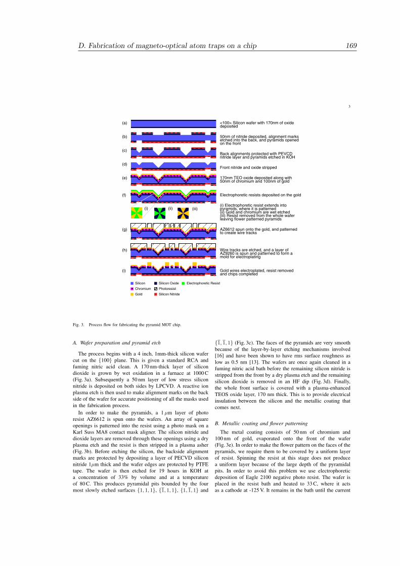
3
<100> Silicon wafer with 170nm of oxide deposited
50nm of nitride deposited, alignment marks etched into the back, and pyramids opened on the front
Back alignments protected with PEVCD nitride layer and pyramids etched in KOH
Front nitride and oxide stripped
170nm TEO oxide deposited along with 50nm of chromium and 100nm of gold
Electrophoretic resists deposited on the gold
(i) Electrophoretic resist extends into pyramids, where it is patterned(ii) Gold and chromium are wet etched(iii) Resist removed from the whole wafer leaving flower patterned pyramids
AZ6612 spun onto the gold, and patterned to create wire tracks
Wire tracks are etched, and a layer of AZ9260 is spun and patterned to form a mold for electroplating
Gold wires electroplated, resist removed and chips completed
(i) (ii) (iii)
Silicon
Chromium
Gold
Silicon Oxide
Photoresist
Silicon Nitride
Electrophoretic Resist
(a)
(b)
(c)
(d)
(e)
(f)
(g)
(h)
(i)
Fig. 3. Process flow for fabricating the pyramid MOT chip.
A. Wafer preparation and pyramid etch
The process begins with a 4 inch, 1mm-thick silicon wafercut on the {100} plane. This is given a standard RCA andfuming nitric acid clean. A 170 nm-thick layer of silicondioxide is grown by wet oxidation in a furnace at 1000 C(Fig. 3a). Subsequently a 50 nm layer of low stress siliconnitride is deposited on both sides by LPCVD. A reactive ionplasma etch is then used to make alignment marks on the backside of the wafer for accurate positioning of all the masks usedin the fabrication process.
In order to make the pyramids, a 1 µm layer of photoresist AZ6612 is spun onto the wafers. An array of squareopenings is patterned into the resist using a photo mask on aKarl Suss MA8 contact mask aligner. The silicon nitride anddioxide layers are removed through these openings using a dryplasma etch and the resist is then stripped in a plasma asher(Fig. 3b). Before etching the silicon, the backside alignmentmarks are protected by depositing a layer of PECVD siliconnitride 1µm thick and the wafer edges are protected by PTFEtape. The wafer is then etched for 19 hours in KOH ata concentration of 33% by volume and at a temperatureof 80 C. This produces pyramidal pits bounded by the fourmost slowly etched surfaces {1, 1, 1}, {1, 1, 1}, {1, 1, 1} and
{1, 1, 1} (Fig. 3c). The faces of the pyramids are very smoothbecause of the layer-by-layer etching mechanisms involved[16] and have been shown to have rms surface roughness aslow as 0.5 nm [13]. The wafers are once again cleaned in afuming nitric acid bath before the remaining silicon nitride isstripped from the front by a dry plasma etch and the remainingsilicon dioxide is removed in an HF dip (Fig. 3d). Finally,the whole front surface is covered with a plasma-enhancedTEOS oxide layer, 170 nm thick. This is to provide electricalinsulation between the silicon and the metallic coating thatcomes next.
B. Metallic coating and flower patterning
The metal coating consists of 50 nm of chromium and100 nm of gold, evaporated onto the front of the wafer(Fig. 3e). In order to make the flower pattern on the faces of thepyramids, we require them to be covered by a uniform layerof resist. Spinning the resist at this stage does not producea uniform layer because of the large depth of the pyramidalpits. In order to avoid this problem we use electrophoreticdeposition of Eagle 2100 negative photo resist. The wafer isplaced in the resist bath and heated to 33 C, where it actsas a cathode at -125 V. It remains in the bath until the current
D. Fabrication of magneto-optical atom traps on a chip 169
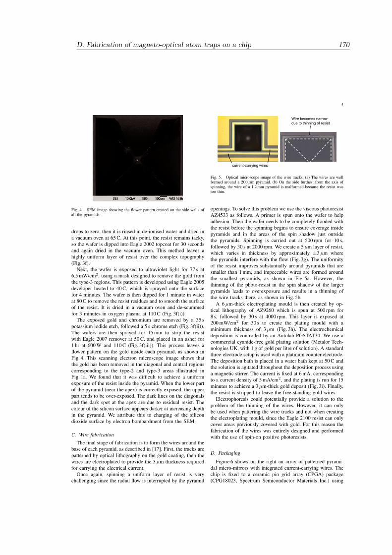
4
Fig. 4. SEM image showing the flower pattern created on the side walls ofall the pyramids.
drops to zero, then it is rinsed in de-ionised water and dried ina vacuum oven at 65 C. At this point, the resist remains tacky,so the wafer is dipped into Eagle 2002 topcoat for 30 secondsand again dried in the vacuum oven. This method leaves ahighly uniform layer of resist over the complex topography(Fig. 3f).
Next, the wafer is exposed to ultraviolet light for 77 s at6.5 mW/cm2, using a mask designed to remove the gold fromthe type-3 regions. This pattern is developed using Eagle 2005developer heated to 40 C, which is sprayed onto the surfacefor 4 minutes. The wafer is then dipped for 1 minute in waterat 80 C to remove the resist residues and to smooth the surfaceof the resist. It is dried in a vacuum oven and de-scummedfor 3 minutes in oxygen plasma at 110 C (Fig. 3f(i)).
The exposed gold and chromium are removed by a 35 spotassium iodide etch, followed a 5 s chrome etch (Fig. 3f(ii)).The wafers are then sprayed for 15 min to strip the resistwith Eagle 2007 remover at 50 C, and placed in an asher for1 hr at 600 W and 110 C (Fig. 3f(iii)). This process leaves aflower pattern on the gold inside each pyramid, as shown inFig. 4. This scanning electron microscope image shows thatthe gold has been removed in the diagonal and central regionscorresponding to the type-2 and type-3 areas illustrated inFig. 1a. We found that it was difficult to achieve a uniformexposure of the resist inside the pyramid. When the lower partof the pyramid (near the apex) is correctly exposed, the upperpart tends to be over-exposed. The dark lines on the diagonalsand the dark spot at the apex are due to residual resist. Thecolour of the silicon surface appears darker at increasing depthin the pyramid. We attribute this to charging of the silicondioxide surface by electron bombardment from the SEM.
C. Wire fabricationThe final stage of fabrication is to form the wires around the
base of each pyramid, as described in [17]. First, the tracks arepatterned by optical lithography on the gold coating, then thewires are electroplated to provide the 3 µm thickness requiredfor carrying the electrical current.
Once again, spinning a uniform layer of resist is verychallenging since the radial flow is interrupted by the pyramid
current-carrying wires
Wire becomes narrowdue to thinning of resist
Fig. 5. Optical microscope image of the wire tracks. (a) The wires are wellformed around a 200 µm pyramid. (b) On the side furthest from the axis ofspinning, the wire of a 1.2 mm pyramid is malformed because the resist wastoo thin.
openings. To solve this problem we use the viscous photoresistAZ4533 as follows. A primer is spun onto the wafer to helpadhesion. Then the wafer needs to be completely flooded withthe resist before the spinning begins to ensure coverage insidepyramids and in the areas of the spin shadow just outsidethe pyramids. Spinning is carried out at 500 rpm for 10 s,followed by 30 s at 2000 rpm. We create a 5 µm layer of resist,which varies in thickness by approximately ±3 µm wherethe pyramids interfere with the flow (Fig. 3g). The uniformityof the resist improves substantially around pyramids that aresmaller than 1 mm, and impeccable wires are formed aroundthe smallest pyramids, as shown in Fig. 5a. However, thethinning of the photo-resist in the spin shadow of the largerpyramids leads to overexposure and results in a thinning ofthe wire tracks there, as shown in Fig. 5b.
A 6 µm-thick electroplating mould is then created by op-tical lithography of AZ9260 which is spun at 500 rpm for8 s, followed by 30 s at 4000 rpm. This layer is exposed at200 mW/cm2 for 30 s to create the plating mould with aminimum thickness of 3 µm (Fig. 3h). The electrochemicaldeposition is controlled by an Autolab PGSTAT30. We use acommercial cyanide-free gold plating solution (Metalor Tech-nologies UK, with 1 g of gold per litre of solution). A standardthree-electrode setup is used with a platinum counter electrode.The deposition bath is placed in a water bath kept at 50 C andthe solution is agitated throughout the deposition process usinga magnetic stirrer. The current is fixed at 6 mA, correspondingto a current density of 5 mA/cm2, and the plating is run for 15minutes to achieve a 3 µm-thick gold deposit (Fig. 3i). Finally,the resist is stripped to leave the free-standing gold wires.
Electrophoresis could potentially provide a solution to theproblem of the thinning of the wires. However, it can onlybe used when pattering the wire tracks and not when creatingthe electroplating mould, since the Eagle 2100 resist can onlycover areas previously covered with gold. For this reason thefabrication of the wires was entirely designed and performedwith the use of spin-on positive photoresists.
D. Packaging
Figure 6 shows on the right an array of patterned pyrami-dal micro-mirrors with integrated current-carrying wires. Thechip is fixed to a ceramic pin grid array (CPGA) package(CPG18023, Spectrum Semiconductor Materials Inc.) using
D. Fabrication of magneto-optical atom traps on a chip 170
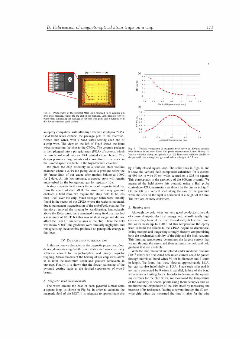
5
32.6 mm
1 mm
Fig. 6. Photographs of the pyramid-MOT chip mounted in its ceramic pingrid array package. Right: the the chip in its package. Left: detailed view ofbond wires connecting the package to the chip wire pads, and a pyramid withthe flower-patterned gold coating.
an epoxy compatible with ultra-high vacuum (Bylapox 7285).Gold bond wires connect the package pins to the microfab-ricated chip wires, with 9 bond wires serving each end ofa chip wire. The view on the left of Fig. 6 shows the bondwires connecting the chip to the CPGA. The ceramic packageis then plugged into a pin grid array (PGA) of sockets, whichin turn is soldered into an FR4 printed circuit board. Thisdesign permits a large number of connections to be made inthe limited space available in the high-vacuum chamber.
We place the chip assembly in a stainless steel vacuumchamber where a 20 l/s ion pump yields a pressure below the10"9mbar limit of our gauge after modest baking at 100 Cfor 2 days. At this low pressure, a trapped atom will remainundisturbed by the background gas for typically 10 s.
A stray magnetic field moves the zeros of magnetic field thatform the centre of each MOT. To ensure that every pyramidencloses a field zero, we require the stray field to be lessthan 10 µT over the chip. Much stronger fields were initiallyfound in the recess of the CPGA where the wafer is mounted,due to permanent magnetisation of the nickel/gold coating. Wetherefore removed the coating by sandblasting. Immediatelyabove the Kovar pins, there remained a stray field that reacheda maximum of 10 µT, but this was of short range and did notaffect the 3 cm x 3 cm active area of the chip. There the fieldwas below 500 nT, the gradients were similarly negligible, andremagnetising the assembly produced no perceptible change atthat level.
IV. DEVICE CHARACTERISATION
In this section we characterise the magnetic properties of ourdevice, demonstrating that the micro-fabricated wires can carrysufficient current for magneto-optical and purely magnetictrapping. Measurements of the heating of our chip wires allowus to infer the maximum depth and gradient achievable inour trap. Finally, it is shown that the flower patterning of thepyramid coating leads to the desired suppression of type-3beams.
A. Magnetic field measurementsThe wires around the base of each pyramid almost form
a square loop, as shown in Fig. 5a. In order to calculate themagnetic field of the MOT, it is adequate to approximate this
0.0 0.3 0.6 0.9 1.2 1.5 1.8
0
1
2
3
4
5
-1.0 -0.5 0.0 0.5 1.0
0.0
0.2
0.4
0.6
0.8
1.0
1.2
B F
ield
(G
)
Vertical Displacement (mm)
(a)
(b)
B F
ield
(G
)
Horizontal Displacement (mm)
Fig. 7. Vertical component of magnetic field above an 800 µm pyramidwith 480 mA in the wire. Dots: Hall probe measurement. Lines: Theory. (a)Vertical variation along the pyramid axis. (b) Transverse variation parallel tothe pyramid row, through the pyramid axis at a height of 0.7 mm.
by a fully closed square loop. The solid lines in Figs. 7a andb show the vertical field component calculated for a currentof 480 mA in wire 50 µm wide, centred on a 895 µm square.This corresponds to the geometry of the 800 µm pyramid. Wemeasured the field above this pyramid using a Hall probe(Lakeshore 421 Gaussmeter), as shown by the circles in Fig. 7.On the left is a vertical scan along the axis of the pyramid,while the scan on the right is horizontal at a height of 0.7 mm.The two are entirely consistent.
B. Heating testsAlthough the gold wires are very good conductors, they do
of course dissipate electrical energy and, at sufficiently highcurrents, they blow like a fuse. Considerably below that limit,the wafer heats up to 120 C. At this temperature the epoxyused to bond the silicon to the CPGA begins to decompose,losing strength and outgassing strongly, thereby compromisingboth the mechanical stability of the chip and the high vacuum.This limiting temperature determines the largest current thatwe run through the wires, and thereby limits the field and fieldgradient that are available.
With the chip mounted and placed under moderate vacuum(10"5 mbar), we first tested how much current could be passedthrough individual bond wires 50 µm in diameter and 2-3 mmin length. We found that these blow at approximately 1.8 A,but can survive indefinitely at 1.5 A. Since each chip pad isnormally connected by 9 wires in parallel, failure of the bondwires is not a limiting factor. In order to determine the operat-ing currents for the chip wires, we monitored the temperatureof the assembly at several points using thermocouples and wemonitored the temperature of the wire itself by measuring theincrease of its resistance. Passing a current through the 50 µm-wide chip wires, we measured the time it takes for the wire
D. Fabrication of magneto-optical atom traps on a chip 171
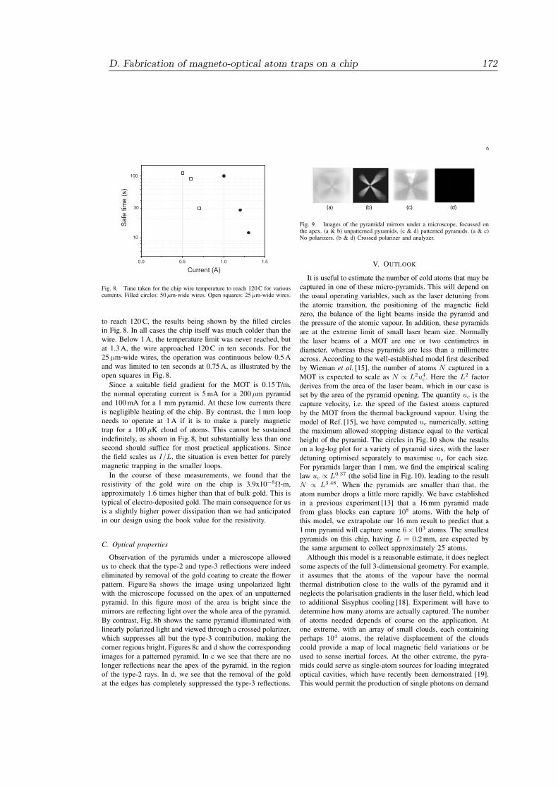
6
0.0 0.5 1.0 1.5
10
100
Saf
e tim
e (s
)
Current (A)
30
Fig. 8. Time taken for the chip wire temperature to reach 120 C for variouscurrents. Filled circles: 50 µm-wide wires. Open squares: 25 µm-wide wires.
to reach 120 C, the results being shown by the filled circlesin Fig. 8. In all cases the chip itself was much colder than thewire. Below 1 A, the temperature limit was never reached, butat 1.3 A, the wire approached 120 C in ten seconds. For the25 µm-wide wires, the operation was continuous below 0.5 Aand was limited to ten seconds at 0.75 A, as illustrated by theopen squares in Fig. 8.
Since a suitable field gradient for the MOT is 0.15 T/m,the normal operating current is 5 mA for a 200 µm pyramidand 100 mA for a 1 mm pyramid. At these low currents thereis negligible heating of the chip. By contrast, the 1 mm loopneeds to operate at 1 A if it is to make a purely magnetictrap for a 100 µK cloud of atoms. This cannot be sustainedindefinitely, as shown in Fig. 8, but substantially less than onesecond should suffice for most practical applications. Sincethe field scales as I/L, the situation is even better for purelymagnetic trapping in the smaller loops.
In the course of these measurements, we found that theresistivity of the gold wire on the chip is 3.9x10"8!-m,approximately 1.6 times higher than that of bulk gold. This istypical of electro-deposited gold. The main consequence for usis a slightly higher power dissipation than we had anticipatedin our design using the book value for the resistivity.
C. Optical properties
Observation of the pyramids under a microscope allowedus to check that the type-2 and type-3 reflections were indeedeliminated by removal of the gold coating to create the flowerpattern. Figure 8a shows the image using unpolarized lightwith the microscope focussed on the apex of an unpatternedpyramid. In this figure most of the area is bright since themirrors are reflecting light over the whole area of the pyramid.By contrast, Fig. 8b shows the same pyramid illuminated withlinearly polarized light and viewed through a crossed polarizer,which suppresses all but the type-3 contribution, making thecorner regions bright. Figures 8c and d show the correspondingimages for a patterned pyramid. In c we see that there are nolonger reflections near the apex of the pyramid, in the regionof the type-2 rays. In d, we see that the removal of the goldat the edges has completely suppressed the type-3 reflections.
(a) (b) (c) (d)
Fig. 9. Images of the pyramidal mirrors under a microscope, focussed onthe apex. (a & b) unpatterned pyramids, (c & d) patterned pyramids. (a & c)No polarizers. (b & d) Crossed polarizer and analyzer.
V. OUTLOOK
It is useful to estimate the number of cold atoms that may becaptured in one of these micro-pyramids. This will depend onthe usual operating variables, such as the laser detuning fromthe atomic transition, the positioning of the magnetic fieldzero, the balance of the light beams inside the pyramid andthe pressure of the atomic vapour. In addition, these pyramidsare at the extreme limit of small laser beam size. Normallythe laser beams of a MOT are one or two centimetres indiameter, whereas these pyramids are less than a millimetreacross. According to the well-established model first describedby Wieman et al. [15], the number of atoms N captured in aMOT is expected to scale as N ! L2u4
c . Here the L2 factorderives from the area of the laser beam, which in our case isset by the area of the pyramid opening. The quantity uc is thecapture velocity, i.e. the speed of the fastest atoms capturedby the MOT from the thermal background vapour. Using themodel of Ref. [15], we have computed uc numerically, settingthe maximum allowed stopping distance equal to the verticalheight of the pyramid. The circles in Fig. 10 show the resultson a log-log plot for a variety of pyramid sizes, with the laserdetuning optimised separately to maximise uc for each size.For pyramids larger than 1 mm, we find the empirical scalinglaw uc ! L0.37 (the solid line in Fig. 10), leading to the resultN ! L3.48. When the pyramids are smaller than that, theatom number drops a little more rapidly. We have establishedin a previous experiment [13] that a 16 mm pyramid madefrom glass blocks can capture 108 atoms. With the help ofthis model, we extrapolate our 16 mm result to predict that a1 mm pyramid will capture some 6" 103 atoms. The smallestpyramids on this chip, having L = 0.2 mm, are expected bythe same argument to collect approximately 25 atoms.
Although this model is a reasonable estimate, it does neglectsome aspects of the full 3-dimensional geometry. For example,it assumes that the atoms of the vapour have the normalthermal distribution close to the walls of the pyramid and itneglects the polarisation gradients in the laser field, which leadto additional Sisyphus cooling [18]. Experiment will have todetermine how many atoms are actually captured. The numberof atoms needed depends of course on the application. Atone extreme, with an array of small clouds, each containingperhaps 104 atoms, the relative displacement of the cloudscould provide a map of local magnetic field variations or beused to sense inertial forces. At the other extreme, the pyra-mids could serve as single-atom sources for loading integratedoptical cavities, which have recently been demonstrated [19].This would permit the production of single photons on demand
D. Fabrication of magneto-optical atom traps on a chip 172
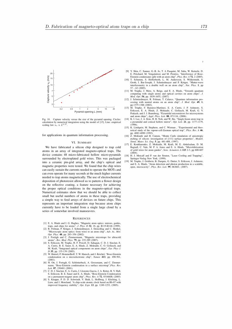
7
0.2 0.5 1 2 5
5
7
10
15
20
3
10 20Pyramid opening L (mm)
Cap
ture
vel
ocity
uc
(m/s
)
Fig. 10. Capture velocity versus the size of the pyramid opening. Circles:calculation by numerical integration using the model of [15]. Line: empiricalscaling law uc ! L0.37.
for applications in quantum information processing.
VI. SUMMARY
We have fabricated a silicon chip designed to trap coldatoms in an array of integrated magneto-optical traps. Thedevice contains 48 micro-fabricated hollow micro-pyramidssurrounded by electroplated gold wires. This was packagedinto a ceramic pin-grid array, and the chip’s optical andmagnetic properties were tested. We found that the chip wirescan easily sustain the currents needed to operate the MOTs andcan even operate for many seconds at the much higher currentsneeded to trap atoms magnetically. The use of electrochemicaldeposition of photoresist allowed us to pattern a flower designon the reflective coating, a feature necessary for achievingthe proper optical conditions in the magneto-optical traps.Numerical estimates show that we should be able to collectsmall but useful numbers of atoms in these traps, providinga simple way to feed arrays of devices on future chips. Thisrepresents an important integration step because atom chipscurrently have to be loaded from a single large cloud by aseries of somewhat involved manoeuvres.
REFERENCES
[1] E. A. Hinds and I. G. Hughes, “Magnetic atom optics: mirrors, guides,traps, and chips for atoms”, J. Phys. D 32, 18, pp. R119-R146 (1999).
[2] R. Folman, P. Kruger, J. Schmiedmayer, J. Denschlag and C. Henkel,“Microscopic atom optics: from wires to an atom chip”, Adv. At., Mol.Opt. Phys. 48, pp. 263–356 (2002).
[3] J. Fortagh and C. Zimmermann, “Magnetic microtraps for ultracoldatoms”, Rev. Mod. Phys. 79, pp. 235-289 (2007).
[4] S. Eriksson, M. Trupke, H. F. Powell, D. Sahagun, C. D. J. Sinclair, E.A. Curtis, B. E. Sauer, E. A. Hinds, Z. Moktadir, C. O. Gollasch, andM. Kraft, “Integrated optical components on atom chips”, Eur. Phys J.D 35, pp. 135-139 (2005).
[5] W. Hansel, P. Hommelhoff, T. W. Hansch, and J. Reichel, “Bose-Einsteincondensation on a microelectronic chip”, Nature 413, pp. 498-501,(2001).
[6] H. Ott, J. Fortagh, G. Schlotterbeck, A. Grossmann, and C. Zimmer-mann, “Bose-Einstein condensation in a surface microtrap”,Phys. Rev.Lett. 87, 230401 (2001).
[7] C. D. J. Sinclair, E. A. Curtis, I. Llorente-Garcia, J. A. Retter, B. V. Hall,S. Eriksson, B. E. Sauer and E. A. Hinds, “Bose-Einstein Condensationon a permanent-magnet atom chip”, Phys. Rev. A 72, 03160(R) (2005)
[8] S. Knappe, P. D. D. Schwindt, V. Shah, L. Hollberg, J. Kitching, L.Liew, and J. Moreland, “A chip-scale atomic clock based on Rb-87 withimproved frequency stability”, Opt. Expr. 13, pp. 1249-1253, (2005).
[9] Y. Shin, C. Sanner, G.-B. Jo, T. A Pasquini, M. Saba, W. Ketterle, D.E. Pritchard, M. Vengalattore and M. Prentiss, “Interference of Bose-Einstein condensates split with an atom chip”, Phys. Rev. A 72, 2 (2005).
[10] T. Schumm, S. Hofferberth, L. M. Andersson, S. Wildermuth, S.Groth, I. Bar-Joseph, J. Schmiedmayer and P. Kruger, “Matter-waveinterferometry in a double well on an atom chip”, Nat. Phys. 1, pp57 - 62 (2005).
[11] M. Trupke, J. Metz, A. Beige, and E. A. Hinds, “Towards quantumcomputing with single atoms and optical cavities on atom chips”, J.Mod. Opt. 54, pp. 1639-1655, (2007).
[12] J. Schmiedmayer, R. Folman, T. Calarco, “Quantum information pro-cessing with neutral atoms on an atom chip”, J. Mod. Opt. 49, 8,pp.1375-1388 (2002).
[13] M. Trupke, F. Ramirez-Martinez, E. A. Curtis, J. P. Ashmore, S.Eriksson, E. A. Hinds, Z. Moktadir, C. Gollasch, M. Kraft, G. V.Prakash, and J. J. Baumberg, “Pyramidal micromirrors for microsystemsand atom chips”, Appl. Phys. Lett. 88, 071116, (2006).
[14] K. I. Lee, J. A. Kim, H. R. Noh, and W. Jhe, “Single-beam atom trap ina pyramidal and conical hollow mirror”, Opt. Lett. 21, pp. 1177-1179,(1996).
[15] K. Lindquist, M. Stephens, and C. Wieman , “Experimental and theo-retical study of the vapour-cell-Zeeman optical trap”, Phys. Rev. A 46,pp. 4082-4090 (1992).
[16] Z. Moktadir and H. Camon, “Monte Carlo simulation of anisotropicetching of silicon: investigation of [111] surface properties”, Modell.Simul. Mater. Sci. Eng. 5, pp. 481-488, (1997).
[17] E. Koukharenko, Z. Moktadir, M. Kraft, M. E. Abdelsalam, D. M.Bagnall, C. Vale, M. P. A. Jones and E. A. Hinds, “Microfabricationof gold wires for atom guides”, Sens. Actuators A 115 2-3, pp 600-607(2004).
[18] H. J. Metcalf and P. van der Straten, ”Laser Cooling and Trapping”,Springer-Verlag New York. (1999).
[19] M. Trupke, J. Goldwin, B. Darquie, G. Dutier, S. Eriksson, J. Ashmore,and E. A. Hinds, “Atom detection and photon production in a scalable,open, microcavity”, Phys. Rev. Lett. 99, 063601, (2007).
D. Fabrication of magneto-optical atom traps on a chip 173
174
Appendix E
Micron-sized atom traps madefrom magneto-optical thin films
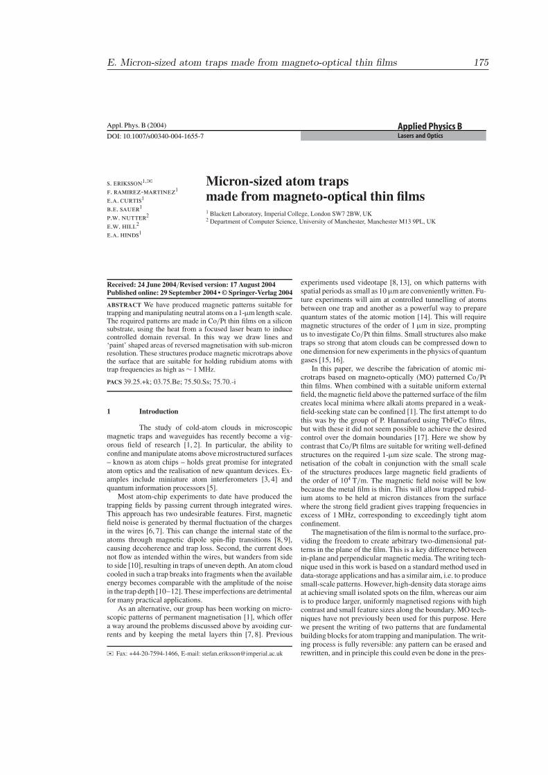
DOI: 10.1007/s00340-004-1655-7
Appl. Phys. B (2004)Lasers and OpticsApplied Physics B
s. eriksson1,!
f. ramirez-martinez1
e.a. curtis1
b.e. sauer1
p.w. nutter2
e.w. hill2
e.a. hinds1
Micron-sized atom trapsmade from magneto-optical thin films1 Blackett Laboratory, Imperial College, London SW7 2BW, UK2 Department of Computer Science, University of Manchester, Manchester M13 9PL, UK
Received: 24 June 2004/Revised version: 17 August 2004Published online: 29 September 2004 • © Springer-Verlag 2004
ABSTRACT We have produced magnetic patterns suitable fortrapping and manipulating neutral atoms on a 1-µm length scale.The required patterns are made in Co/Pt thin films on a siliconsubstrate, using the heat from a focused laser beam to inducecontrolled domain reversal. In this way we draw lines and‘paint’ shaped areas of reversed magnetisation with sub-micronresolution. These structures produce magnetic microtraps abovethe surface that are suitable for holding rubidium atoms withtrap frequencies as high as ! 1 MHz.
PACS 39.25.+k; 03.75.Be; 75.50.Ss; 75.70.-i
1 Introduction
The study of cold-atom clouds in microscopicmagnetic traps and waveguides has recently become a vig-orous field of research [1, 2]. In particular, the ability toconfine and manipulate atoms above microstructured surfaces– known as atom chips – holds great promise for integratedatom optics and the realisation of new quantum devices. Ex-amples include miniature atom interferometers [3, 4] andquantum information processors [5].
Most atom-chip experiments to date have produced thetrapping fields by passing current through integrated wires.This approach has two undesirable features. First, magneticfield noise is generated by thermal fluctuation of the chargesin the wires [6, 7]. This can change the internal state of theatoms through magnetic dipole spin-flip transitions [8, 9],causing decoherence and trap loss. Second, the current doesnot flow as intended within the wires, but wanders from sideto side [10], resulting in traps of uneven depth. An atom cloudcooled in such a trap breaks into fragments when the availableenergy becomes comparable with the amplitude of the noisein the trap depth [10–12]. These imperfections are detrimentalfor many practical applications.
As an alternative, our group has been working on micro-scopic patterns of permanent magnetisation [1], which offera way around the problems discussed above by avoiding cur-rents and by keeping the metal layers thin [7, 8]. Previous
! Fax: +44-20-7594-1466, E-mail: [email protected]
experiments used videotape [8, 13], on which patterns withspatial periods as small as 10 µm are conveniently written. Fu-ture experiments will aim at controlled tunnelling of atomsbetween one trap and another as a powerful way to preparequantum states of the atomic motion [14]. This will requiremagnetic structures of the order of 1 µm in size, promptingus to investigate Co/Pt thin films. Small structures also maketraps so strong that atom clouds can be compressed down toone dimension for new experiments in the physics of quantumgases [15, 16].
In this paper, we describe the fabrication of atomic mi-crotraps based on magneto-optically (MO) patterned Co/Ptthin films. When combined with a suitable uniform externalfield, the magnetic field above the patterned surface of the filmcreates local minima where alkali atoms prepared in a weak-field-seeking state can be confined [1]. The first attempt to dothis was by the group of P. Hannaford using TbFeCo films,but with these it did not seem possible to achieve the desiredcontrol over the domain boundaries [17]. Here we show bycontrast that Co/Pt films are suitable for writing well-definedstructures on the required 1-µm size scale. The strong mag-netisation of the cobalt in conjunction with the small scaleof the structures produces large magnetic field gradients ofthe order of 104 T/m. The magnetic field noise will be lowbecause the metal film is thin. This will allow trapped rubid-ium atoms to be held at micron distances from the surfacewhere the strong field gradient gives trapping frequencies inexcess of 1 MHz, corresponding to exceedingly tight atomconfinement.
The magnetisation of the film is normal to the surface, pro-viding the freedom to create arbitrary two-dimensional pat-terns in the plane of the film. This is a key difference betweenin-plane and perpendicular magnetic media. The writing tech-nique used in this work is based on a standard method used indata-storage applications and has a similar aim, i.e. to producesmall-scale patterns. However, high-density data storage aimsat achieving small isolated spots on the film, whereas our aimis to produce larger, uniformly magnetised regions with highcontrast and small feature sizes along the boundary. MO tech-niques have not previously been used for this purpose. Herewe present the writing of two patterns that are fundamentalbuilding blocks for atom trapping and manipulation. The writ-ing process is fully reversible: any pattern can be erased andrewritten, and in principle this could even be done in the pres-
E. Micron-sized atom traps made from magneto-optical thin films 175
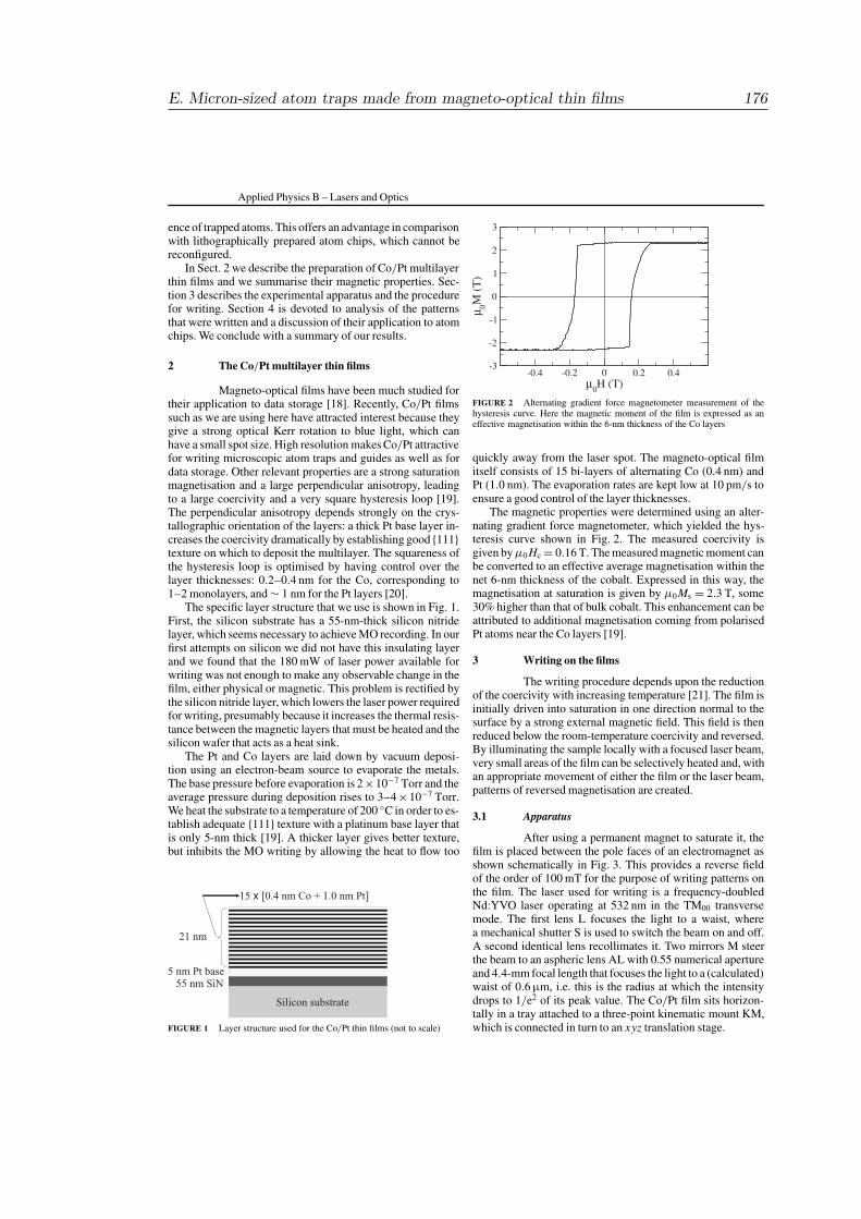
Applied Physics B – Lasers and Optics
ence of trapped atoms. This offers an advantage in comparisonwith lithographically prepared atom chips, which cannot bereconfigured.
In Sect. 2 we describe the preparation of Co/Pt multilayerthin films and we summarise their magnetic properties. Sec-tion 3 describes the experimental apparatus and the procedurefor writing. Section 4 is devoted to analysis of the patternsthat were written and a discussion of their application to atomchips. We conclude with a summary of our results.
2 The Co/Pt multilayer thin films
Magneto-optical films have been much studied fortheir application to data storage [18]. Recently, Co/Pt filmssuch as we are using here have attracted interest because theygive a strong optical Kerr rotation to blue light, which canhave a small spot size. High resolution makes Co/Pt attractivefor writing microscopic atom traps and guides as well as fordata storage. Other relevant properties are a strong saturationmagnetisation and a large perpendicular anisotropy, leadingto a large coercivity and a very square hysteresis loop [19].The perpendicular anisotropy depends strongly on the crys-tallographic orientation of the layers: a thick Pt base layer in-creases the coercivity dramatically by establishing good {111}texture on which to deposit the multilayer. The squareness ofthe hysteresis loop is optimised by having control over thelayer thicknesses: 0.2–0.4 nm for the Co, corresponding to1–2 monolayers, and ! 1 nm for the Pt layers [20].
The specific layer structure that we use is shown in Fig. 1.First, the silicon substrate has a 55-nm-thick silicon nitridelayer, which seems necessary to achieve MO recording. In ourfirst attempts on silicon we did not have this insulating layerand we found that the 180 mW of laser power available forwriting was not enough to make any observable change in thefilm, either physical or magnetic. This problem is rectified bythe silicon nitride layer, which lowers the laser power requiredfor writing, presumably because it increases the thermal resis-tance between the magnetic layers that must be heated and thesilicon wafer that acts as a heat sink.
The Pt and Co layers are laid down by vacuum deposi-tion using an electron-beam source to evaporate the metals.The base pressure before evaporation is 2 "10#7 Torr and theaverage pressure during deposition rises to 3–4 "10#7 Torr.We heat the substrate to a temperature of 200 $C in order to es-tablish adequate {111} texture with a platinum base layer thatis only 5-nm thick [19]. A thicker layer gives better texture,but inhibits the MO writing by allowing the heat to flow too
FIGURE 1 Layer structure used for the Co/Pt thin films (not to scale)
FIGURE 2 Alternating gradient force magnetometer measurement of thehysteresis curve. Here the magnetic moment of the film is expressed as aneffective magnetisation within the 6-nm thickness of the Co layers
quickly away from the laser spot. The magneto-optical filmitself consists of 15 bi-layers of alternating Co (0.4 nm) andPt (1.0 nm). The evaporation rates are kept low at 10 pm/s toensure a good control of the layer thicknesses.
The magnetic properties were determined using an alter-nating gradient force magnetometer, which yielded the hys-teresis curve shown in Fig. 2. The measured coercivity isgiven by µ0 Hc = 0.16 T. The measured magnetic moment canbe converted to an effective average magnetisation within thenet 6-nm thickness of the cobalt. Expressed in this way, themagnetisation at saturation is given by µ0Ms = 2.3 T, some30% higher than that of bulk cobalt. This enhancement can beattributed to additional magnetisation coming from polarisedPt atoms near the Co layers [19].
3 Writing on the films
The writing procedure depends upon the reductionof the coercivity with increasing temperature [21]. The film isinitially driven into saturation in one direction normal to thesurface by a strong external magnetic field. This field is thenreduced below the room-temperature coercivity and reversed.By illuminating the sample locally with a focused laser beam,very small areas of the film can be selectively heated and, withan appropriate movement of either the film or the laser beam,patterns of reversed magnetisation are created.
3.1 Apparatus
After using a permanent magnet to saturate it, thefilm is placed between the pole faces of an electromagnet asshown schematically in Fig. 3. This provides a reverse fieldof the order of 100 mT for the purpose of writing patterns onthe film. The laser used for writing is a frequency-doubledNd:YVO laser operating at 532 nm in the TM00 transversemode. The first lens L focuses the light to a waist, wherea mechanical shutter S is used to switch the beam on and off.A second identical lens recollimates it. Two mirrors M steerthe beam to an aspheric lens AL with 0.55 numerical apertureand 4.4-mm focal length that focuses the light to a (calculated)waist of 0.6 µm, i.e. this is the radius at which the intensitydrops to 1/e2 of its peak value. The Co/Pt film sits horizon-tally in a tray attached to a three-point kinematic mount KM,which is connected in turn to an xyz translation stage.
E. Micron-sized atom traps made from magneto-optical thin films 176
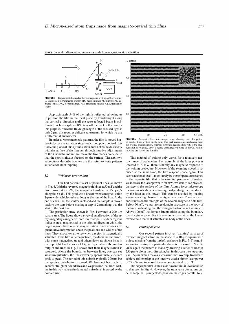
ERIKSSON et al. Micron-sized atom traps made from magneto-optical thin films
FIGURE 3 Experimental setup for thermomagnetic writing. Abbreviations:L, lenses; S, programmable shutter; BS, beam splitter; M, mirrors; AL, as-pheric lens; MAG, electromagnet; KM, kinematic mount; XYZ, translationstages
Approximately 54% of the light is reflected, allowing usto position the film in the focal plane by translating it alongthe vertical z direction until the retro-reflected beam is col-limated. A beam splitter BS picks off the back reflection forthis purpose. Since the Rayleigh length of the focused light isonly 2 µm, this requires delicate adjustment, for which we usea differential micrometer.
In order to write magnetic patterns, the film is moved hor-izontally by a translation stage under computer control. Ini-tially, the plane of this xy translation does not coincide exactlywith the surface of the film but, through iterative adjustmentsof the kinematic mount, we make the two planes coincide sothat the spot is always focused on the surface. The next twosubsections describe how we use this setup to write patternssuitable for atom trapping.
3.2 Writing an array of lines
Our first pattern is a set of parallel lines, as shownin Fig. 4. With the reversed magnetic field set at 50 mT and thelaser power at 75 mW, the sample is translated at 250 µm/salong the x axis. This produces a line of reverse magnetisation1-µm wide, which can be as long as the size of the film. At theend of each line, the shutter is closed and the sample is movedback to the start before making a step of 2 µm along y to thestart of the next line.
The particular array shown in Fig. 4 covered a 200-µmsquare area. The figure shows a typical small section of the ar-ray imaged by a magnetic force microscope. The dark regionsindicate areas magnetised in the original direction whilst thebright regions have reverse magnetisation. Such images givequantitative information about the positions and widths of thelines. They also allow us to see when a region is magneticallysaturated. If the film is demagnetised, the domains are mixed,with some magnetised up and others down as shown inset inthe top right hand corner of Fig. 4. By contrast, the unifor-mity of the lines in Fig. 4 shows that their magnetisation issaturated. Along the boundaries between lines, one can seesmall irregularities: the lines waver by approximately 250 nmpeak-to-peak. The period of this noise is typically 300 nm butthe spectral distribution is broad. We have not been able toachieve straighter boundaries and we presume that lines writ-ten in this way have a fundamental noise level imposed by thedomain size.
FIGURE 4 Magnetic force microscope image showing part of a patternof parallel lines written on the film. The dark regions are unchanged fromthe original magnetisation, whereas the bright regions show where the mag-netisation is reversed. Inset: a nearly demagnetised piece of the Co/Pt film,showing the size of the domains
This method of writing only works for a relatively nar-row range of parameters. For example, if the laser power islowered to 70 mW, there is hardly any magnetic response tothe writing procedure. However, if the scanning speed is re-duced at the same time, the film responds once again. Thisseems reasonable as it must surely be the temperature reachedin the magnetic film that is the essential parameter. If insteadwe increase the laser power to 80 mW, we start to see physicaldamage to the surface of the film. Atomic force microscopemeasurements show a 2-nm-high ridge along the line drawnby the laser at this power. This can be avoided by makinga compensating change to a higher scan rate. There are alsoconstraints on the strength of the reverse magnetic field bias.Below 50 mT, we start to see domain structure in the body ofthe lines, indicating that the remagnetisation is not saturated.Above 100 mT the domain irregularities along the boundarylines begin to grow. For this reason, we operate at the lowestreverse field that still saturates the body of the lines.
3.3 Painting an area
Our second pattern involves ‘painting’ an area ofreversed magnetisation in the shape of a 40-µm square witha piece missing from the top left, as shown in Fig. 5. The moti-vation for making this particular shape is discussed in Sect. 4.Once again the pattern is made by drawing a series of lines at250 µm/s along the x direction, but in this case the step alongy is 0.5 µm, which makes successive lines overlap. In order toachieve full overlap of the lines we used a higher laser powerof 79 mW and increased the reverse-bias field to 0.1 T.
The edges parallel to the x axis have a similar level of noiseto that seen in Fig. 4. However, the transverse deviations canbe as large as 1 µm peak-to-peak on the edges parallel to y.
E. Micron-sized atom traps made from magneto-optical thin films 177
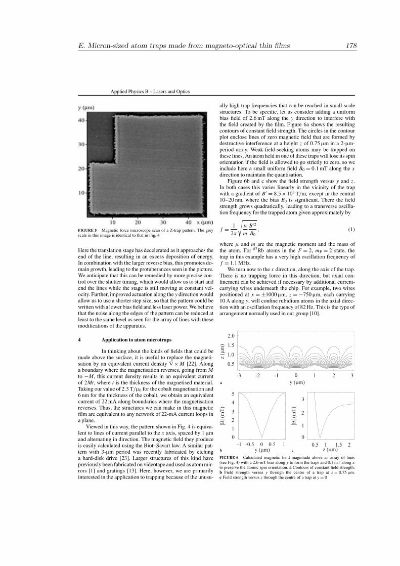
Applied Physics B – Lasers and Optics
FIGURE 5 Magnetic force microscope scan of a Z-trap pattern. The greyscale in this image is identical to that in Fig. 4
Here the translation stage has decelerated as it approaches theend of the line, resulting in an excess deposition of energy.In combination with the larger reverse bias, this promotes do-main growth, leading to the protuberances seen in the picture.We anticipate that this can be remedied by more precise con-trol over the shutter timing, which would allow us to start andend the lines while the stage is still moving at constant vel-ocity. Further, improved actuation along the y direction wouldallow us to use a shorter step size, so that the pattern could bewritten with a lower bias field and less laser power. We believethat the noise along the edges of the pattern can be reduced atleast to the same level as seen for the array of lines with thesemodifications of the apparatus.
4 Application to atom microtraps
In thinking about the kinds of fields that could bemade above the surface, it is useful to replace the magneti-sation by an equivalent current density % " M [22]. Alonga boundary where the magnetisation reverses, going from Mto #M, this current density results in an equivalent currentof 2Mt, where t is the thickness of the magnetised material.Taking our value of 2.3 T/µ0 for the cobalt magnetisation and6 nm for the thickness of the cobalt, we obtain an equivalentcurrent of 22 mA along boundaries where the magnetisationreverses. Thus, the structures we can make in this magneticfilm are equivalent to any network of 22-mA current loops ina plane.
Viewed in this way, the pattern shown in Fig. 4 is equiva-lent to lines of current parallel to the x axis, spaced by 1 µmand alternating in direction. The magnetic field they produceis easily calculated using the Biot–Savart law. A similar pat-tern with 3-µm period was recently fabricated by etchinga hard-disk drive [23]. Larger structures of this kind havepreviously been fabricated on videotape and used as atom mir-rors [1] and gratings [13]. Here, however, we are primarilyinterested in the application to trapping because of the unusu-
ally high trap frequencies that can be reached in small-scalestructures. To be specific, let us consider adding a uniformbias field of 2.6 mT along the y direction to interfere withthe field created by the film. Figure 6a shows the resultingcontours of constant field strength. The circles in the contourplot enclose lines of zero magnetic field that are formed bydestructive interference at a height z of 0.75 µm in a 2-µm-period array. Weak-field-seeking atoms may be trapped onthese lines. An atom held in one of these traps will lose its spinorientation if the field is allowed to go strictly to zero, so weinclude here a small uniform field B0 = 0.1 mT along the xdirection to maintain the quantisation.
Figure 6b and c show the field strength versus y and z.In both cases this varies linearly in the vicinity of the trapwith a gradient of B& = 8.5 "103 T/m, except in the central10–20 nm, where the bias B0 is significant. There the fieldstrength grows quadratically, leading to a transverse oscilla-tion frequency for the trapped atom given approximately by
f = 12!
!µ
mB&2
B0, (1)
where µ and m are the magnetic moment and the mass ofthe atom. For 87Rb atoms in the F = 2, mF = 2 state, thetrap in this example has a very high oscillation frequency off = 1.1 MHz.
We turn now to the x direction, along the axis of the trap.There is no trapping force in this direction, but axial con-finement can be achieved if necessary by additional current-carrying wires underneath the chip. For example, two wirespositioned at x = ±1000 µm, z = #750 µm, each carrying10 A along y, will confine rubidium atoms in the axial direc-tion with an oscillation frequency of 82 Hz. This is the type ofarrangement normally used in our group [10].
c
FIGURE 6 Calculated magnetic field magnitude above an array of lines(see Fig. 4) with a 2.6-mT bias along y to form the traps and 0.1 mT along xto preserve the atomic spin orientation. a Contours of constant field strength.b Field strength versus y through the centre of a trap at z = 0.75 µm.c Field strength versus z through the centre of a trap at y = 0
E. Micron-sized atom traps made from magneto-optical thin films 178
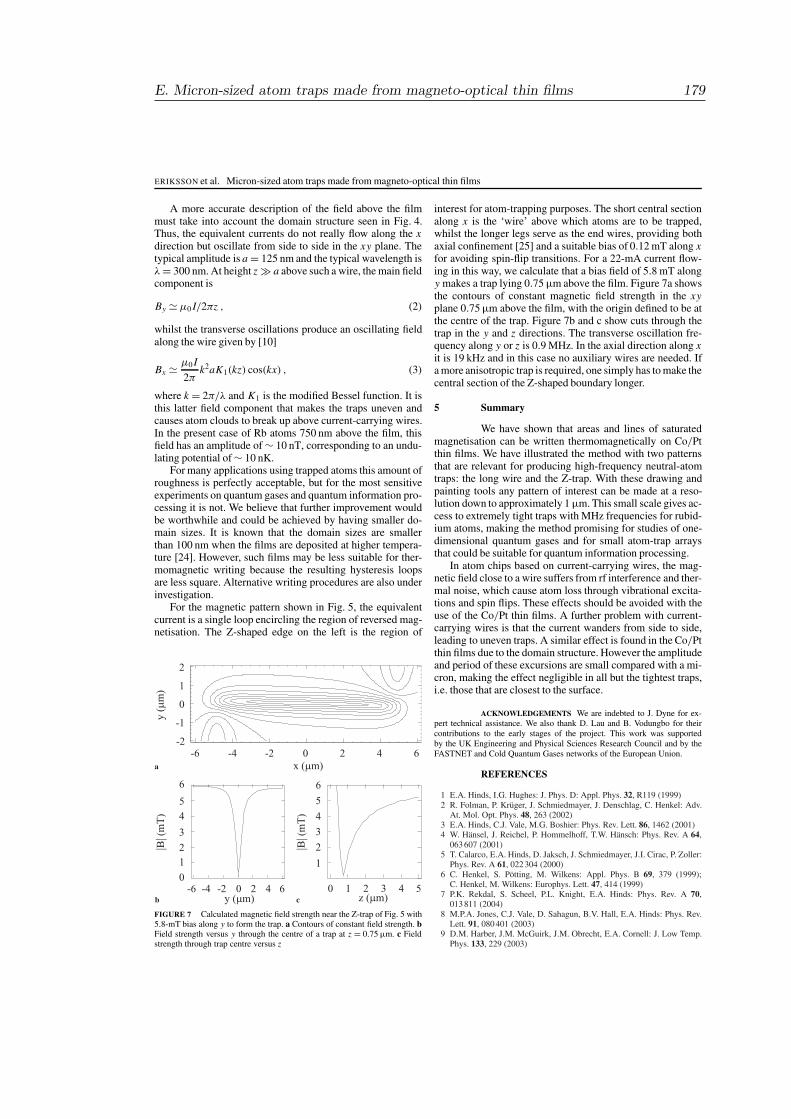
ERIKSSON et al. Micron-sized atom traps made from magneto-optical thin films
A more accurate description of the field above the filmmust take into account the domain structure seen in Fig. 4.Thus, the equivalent currents do not really flow along the xdirection but oscillate from side to side in the xy plane. Thetypical amplitude is a = 125 nm and the typical wavelength is" = 300 nm. At height z ' a above such a wire, the main fieldcomponent is
By ( µ0 I/2!z , (2)
whilst the transverse oscillations produce an oscillating fieldalong the wire given by [10]
Bx ( µ0 I2!
k2aK1(kz) cos(kx) , (3)
where k = 2!/" and K1 is the modified Bessel function. It isthis latter field component that makes the traps uneven andcauses atom clouds to break up above current-carrying wires.In the present case of Rb atoms 750 nm above the film, thisfield has an amplitude of ! 10 nT, corresponding to an undu-lating potential of ! 10 nK.
For many applications using trapped atoms this amount ofroughness is perfectly acceptable, but for the most sensitiveexperiments on quantum gases and quantum information pro-cessing it is not. We believe that further improvement wouldbe worthwhile and could be achieved by having smaller do-main sizes. It is known that the domain sizes are smallerthan 100 nm when the films are deposited at higher tempera-ture [24]. However, such films may be less suitable for ther-momagnetic writing because the resulting hysteresis loopsare less square. Alternative writing procedures are also underinvestigation.
For the magnetic pattern shown in Fig. 5, the equivalentcurrent is a single loop encircling the region of reversed mag-netisation. The Z-shaped edge on the left is the region of
FIGURE 7 Calculated magnetic field strength near the Z-trap of Fig. 5 with5.8-mT bias along y to form the trap. a Contours of constant field strength. bField strength versus y through the centre of a trap at z = 0.75 µm. c Fieldstrength through trap centre versus z
interest for atom-trapping purposes. The short central sectionalong x is the ‘wire’ above which atoms are to be trapped,whilst the longer legs serve as the end wires, providing bothaxial confinement [25] and a suitable bias of 0.12 mT along xfor avoiding spin-flip transitions. For a 22-mA current flow-ing in this way, we calculate that a bias field of 5.8 mT alongy makes a trap lying 0.75 µm above the film. Figure 7a showsthe contours of constant magnetic field strength in the xyplane 0.75 µm above the film, with the origin defined to be atthe centre of the trap. Figure 7b and c show cuts through thetrap in the y and z directions. The transverse oscillation fre-quency along y or z is 0.9 MHz. In the axial direction along xit is 19 kHz and in this case no auxiliary wires are needed. Ifa more anisotropic trap is required, one simply has to make thecentral section of the Z-shaped boundary longer.
5 Summary
We have shown that areas and lines of saturatedmagnetisation can be written thermomagnetically on Co/Ptthin films. We have illustrated the method with two patternsthat are relevant for producing high-frequency neutral-atomtraps: the long wire and the Z-trap. With these drawing andpainting tools any pattern of interest can be made at a reso-lution down to approximately 1 µm. This small scale gives ac-cess to extremely tight traps with MHz frequencies for rubid-ium atoms, making the method promising for studies of one-dimensional quantum gases and for small atom-trap arraysthat could be suitable for quantum information processing.
In atom chips based on current-carrying wires, the mag-netic field close to a wire suffers from rf interference and ther-mal noise, which cause atom loss through vibrational excita-tions and spin flips. These effects should be avoided with theuse of the Co/Pt thin films. A further problem with current-carrying wires is that the current wanders from side to side,leading to uneven traps. A similar effect is found in the Co/Ptthin films due to the domain structure. However the amplitudeand period of these excursions are small compared with a mi-cron, making the effect negligible in all but the tightest traps,i.e. those that are closest to the surface.
ACKNOWLEDGEMENTS We are indebted to J. Dyne for ex-pert technical assistance. We also thank D. Lau and B. Vodungbo for theircontributions to the early stages of the project. This work was supportedby the UK Engineering and Physical Sciences Research Council and by theFASTNET and Cold Quantum Gases networks of the European Union.
REFERENCES
1 E.A. Hinds, I.G. Hughes: J. Phys. D: Appl. Phys. 32, R119 (1999)2 R. Folman, P. Krüger, J. Schmiedmayer, J. Denschlag, C. Henkel: Adv.
At. Mol. Opt. Phys. 48, 263 (2002)3 E.A. Hinds, C.J. Vale, M.G. Boshier: Phys. Rev. Lett. 86, 1462 (2001)4 W. Hänsel, J. Reichel, P. Hommelhoff, T.W. Hänsch: Phys. Rev. A 64,
063 607 (2001)5 T. Calarco, E.A. Hinds, D. Jaksch, J. Schmiedmayer, J.I. Cirac, P. Zoller:
Phys. Rev. A 61, 022 304 (2000)6 C. Henkel, S. Pötting, M. Wilkens: Appl. Phys. B 69, 379 (1999);
C. Henkel, M. Wilkens: Europhys. Lett. 47, 414 (1999)7 P.K. Rekdal, S. Scheel, P.L. Knight, E.A. Hinds: Phys. Rev. A 70,
013 811 (2004)8 M.P.A. Jones, C.J. Vale, D. Sahagun, B.V. Hall, E.A. Hinds: Phys. Rev.
Lett. 91, 080 401 (2003)9 D.M. Harber, J.M. McGuirk, J.M. Obrecht, E.A. Cornell: J. Low Temp.
Phys. 133, 229 (2003)
E. Micron-sized atom traps made from magneto-optical thin films 179
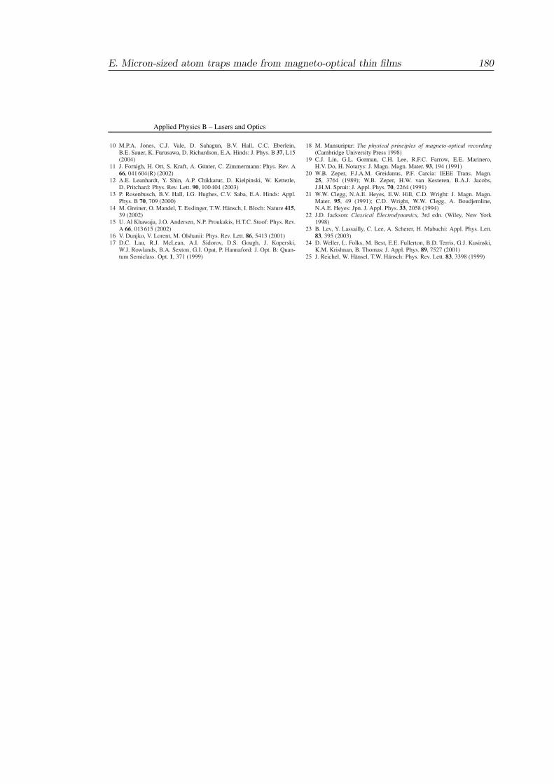
Applied Physics B – Lasers and Optics
10 M.P.A. Jones, C.J. Vale, D. Sahagun, B.V. Hall, C.C. Eberlein,B.E. Sauer, K. Furusawa, D. Richardson, E.A. Hinds: J. Phys. B 37, L15(2004)
11 J. Fortagh, H. Ott, S. Kraft, A. Günter, C. Zimmermann: Phys. Rev. A66, 041 604(R) (2002)
12 A.E. Leanhardt, Y. Shin, A.P. Chikkatur, D. Kielpinski, W. Ketterle,D. Pritchard: Phys. Rev. Lett. 90, 100 404 (2003)
13 P. Rosenbusch, B.V. Hall, I.G. Hughes, C.V. Saba, E.A. Hinds: Appl.Phys. B 70, 709 (2000)
14 M. Greiner, O. Mandel, T. Esslinger, T.W. Hänsch, I. Bloch: Nature 415,39 (2002)
15 U. Al Khawaja, J.O. Andersen, N.P. Proukakis, H.T.C. Stoof: Phys. Rev.A 66, 013 615 (2002)
16 V. Dunjko, V. Lorent, M. Olshanii: Phys. Rev. Lett. 86, 5413 (2001)17 D.C. Lau, R.J. McLean, A.I. Sidorov, D.S. Gough, J. Koperski,
W.J. Rowlands, B.A. Sexton, G.I. Opat, P. Hannaford: J. Opt. B: Quan-tum Semiclass. Opt. 1, 371 (1999)
18 M. Mansuripur: The physical principles of magneto-optical recording(Cambridge University Press 1998)
19 C.J. Lin, G.L. Gorman, C.H. Lee, R.F.C. Farrow, E.E. Marinero,H.V. Do, H. Notarys: J. Magn. Magn. Mater. 93, 194 (1991)
20 W.B. Zeper, F.J.A.M. Greidanus, P.F. Carcia: IEEE Trans. Magn.25, 3764 (1989); W.B. Zeper, H.W. van Kesteren, B.A.J. Jacobs,J.H.M. Spruit: J. Appl. Phys. 70, 2264 (1991)
21 W.W. Clegg, N.A.E. Heyes, E.W. Hill, C.D. Wright: J. Magn. Magn.Mater. 95, 49 (1991); C.D. Wright, W.W. Clegg, A. Boudjemline,N.A.E. Heyes: Jpn. J. Appl. Phys. 33, 2058 (1994)
22 J.D. Jackson: Classical Electrodynamics, 3rd edn. (Wiley, New York1998)
23 B. Lev, Y. Lassailly, C. Lee, A. Scherer, H. Mabuchi: Appl. Phys. Lett.83, 395 (2003)
24 D. Weller, L. Folks, M. Best, E.E. Fullerton, B.D. Terris, G.J. Kusinski,K.M. Krishnan, B. Thomas: J. Appl. Phys. 89, 7527 (2001)
25 J. Reichel, W. Hänsel, T.W. Hänsch: Phys. Rev. Lett. 83, 3398 (1999)
E. Micron-sized atom traps made from magneto-optical thin films 180