integration seminar - portland state universityweb.pdx.edu/~davide/seminar.pdf · gate oxide gate...
TRANSCRIPT

Microelectronic Device Fabrication I (Basic Chemistry and Physics of
Semiconductor Device Fabrication)
Physics 445/545
Integration Seminar
Dec. 1 & 3, 2014

Chip Fabrication
• From bare Si wafers
to fully functional
IC’s requires a
complicated series
of processing
steps.
• Cleanliness
regimen must be
rigorous.
Jack Kilby inspecting a
300 mm wafer (courtesy TI)
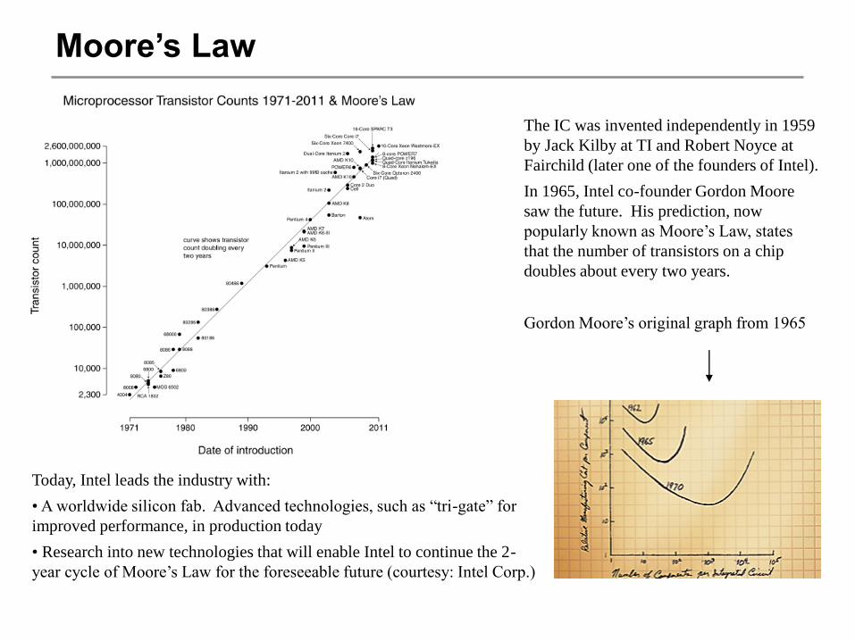
Moore’s Law
The IC was invented independently in 1959
by Jack Kilby at TI and Robert Noyce at
Fairchild (later one of the founders of Intel).
In 1965, Intel co-founder Gordon Moore
saw the future. His prediction, now
popularly known as Moore’s Law, states
that the number of transistors on a chip
doubles about every two years.
Gordon Moore’s original graph from 1965
Today, Intel leads the industry with:
• A worldwide silicon fab. Advanced technologies, such as “tri-gate” for
improved performance, in production today
• Research into new technologies that will enable Intel to continue the 2-
year cycle of Moore’s Law for the foreseeable future (courtesy: Intel Corp.)

Challenge to Moore’s Law
0
5
10
15
20
25
30
35
40
45
650 500 350 250 180 130 100
Generation (nm)
De
lay (
ps
)
Gate Delay
Interconnect Delay
(Al/SiO2)
Interconnect Delay
(Cu/Low k)
Sum of Delays
(Al/SiO2)
Sum of Delays
(Cu/Low k)

SIA Technology Roadmap
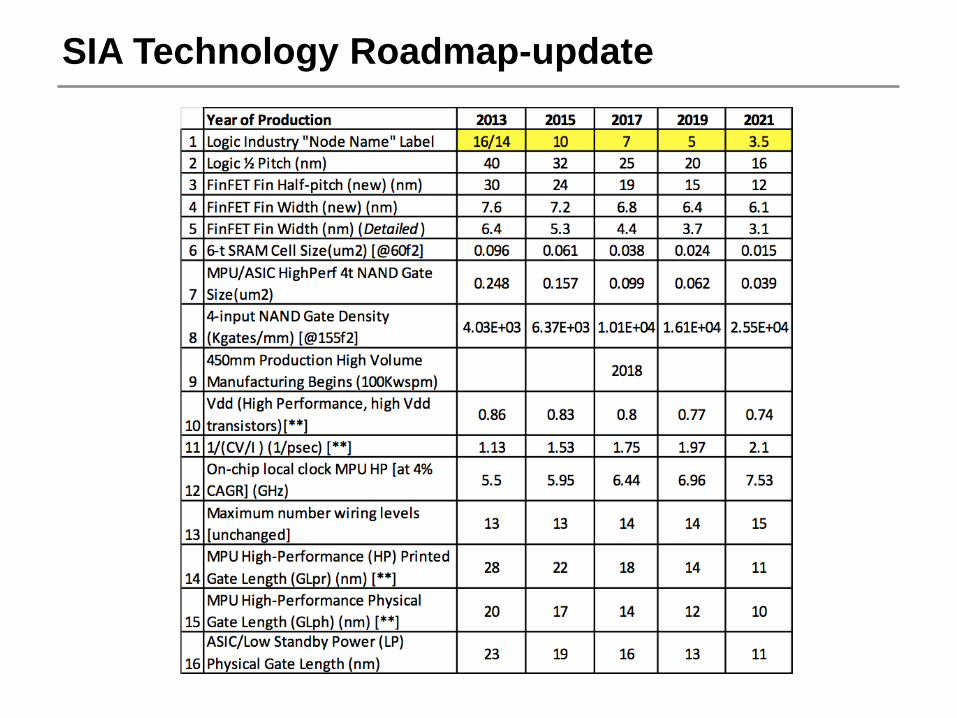
SIA Technology Roadmap-update
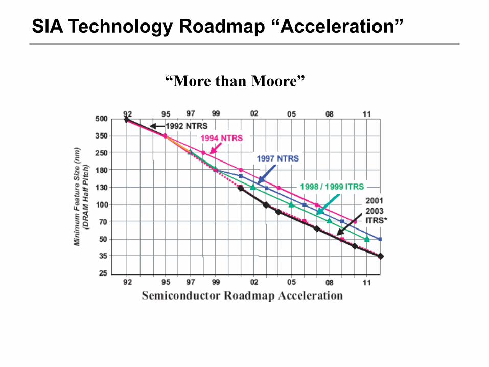
SIA Technology Roadmap “Acceleration”
“More than Moore”

Speculative Future Technologies
Long range roadmap for logic CMOS transistor research
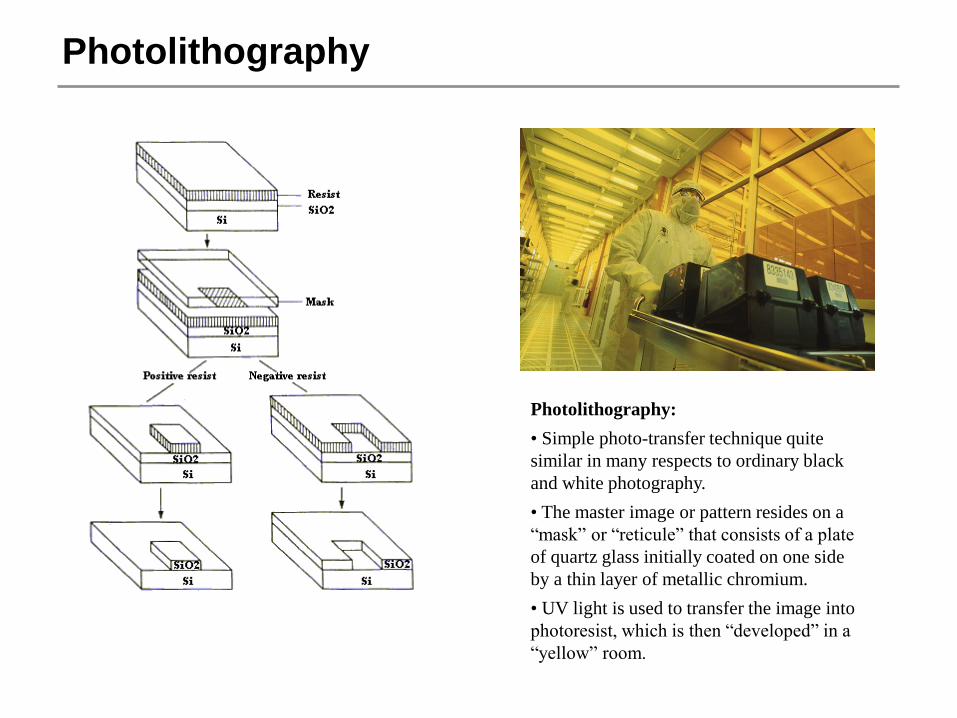
Photolithography
Photolithography:
• Simple photo-transfer technique quite
similar in many respects to ordinary black
and white photography.
• The master image or pattern resides on a
“mask” or “reticule” that consists of a plate
of quartz glass initially coated on one side
by a thin layer of metallic chromium.
• UV light is used to transfer the image into
photoresist, which is then “developed” in a
“yellow” room.

Photolithography – cont’d
Photoresist:
• Negative: remains in exposed area.
Developer: xylene or similar solvent
• Positive: removed in exposed area.
Developer: strong alkaline solution
Exposure Systems:
• Contact: original concept, mask contacts substrate.
• Proximity: improvement of contact to increase
lifetime of mask and reduce “soft” defects.
• Projection: current state-of-the-art – a fully
configured system costs in the neighborhood of M$20.
• Direct write: At one time was considered a competitor
to projection; however, although resolution is high,
throughput is too slow. (Direct write is used for
fabrication of photomasks.)

Photoresist spin-coating
• Photoresist is generally applied to wafers (or other kinds of
substrates) by spin-coating.
• As the term suggests, the idea is quite simple: a solution
containing the resist is dispensed on a spinning substrate,
which then spreads out to form a uniform layer.
• Once the film is coated, it is baked to drive off excess solvent
and stabilize the properties of the film.

Wet Chemical Etching and Cleaning
• Many wet chemical processes are still used in IC fabrication.
• These require strong acids, viz., sulfuric, nitric, hydrochloric,
etc., as well as weaker acids such as acetic and phosphoric.
• Also strong bases, viz., potassium hydroxide or more
recently tetramethyl ammonium hydroxide. Also weaker
bases such as ammonium hydroxide.
• Fluoride chemistry: hydrofluoric acid and ammonium fluoride
• Solvents: acetone, isopropyl alcohol, etc.
• Everyone working fab must be well aware of hazards and
correct handling procedures!!

Dry Etching
Mask
Substrate
Mask
Substrate
Isotropic Etching:
• Requires only the use of simple “wet” chemical
solutions.
• Increases the width of photlithograpically defined
features due to “undercut”. Rule of thumb: size of
undercut equal to depth of etch. (can be much larger).
Anisotropic Etching:
• Includes a directional component, which ideally
allows vertical etching without undercut.
• Cannot be achieved using simple chemical etching,
requires more sophisticated apparatus generally
requiring reduced pressure (a vacuum chamber)
• Because anisotropic etching is generally carried out
using gaseous chemicals it is “dry”.
Plasma Etching
Powered Sheath
Glow
Grounded Sheath
Powered Electrode
Vacuum
Chamber
Grounded Sheath
• Plasma etching uses gaseous chemicals (viz., halocarbons,
halogens, oxygen, etc.) that are activated by a radio
frequency glow discharge.
• The electrical discharge results in the formation of highly
reactive free radical and ionic species that attack the
substrate.
Directionality
+ +
+
+
+ +
+
++
+
++
+
+
+
+
+
++
+
+
+
+
+
+
+
+ + +
+++
+ ++
+
+
+
+
+
++
+
+
++
+
++
+
+
++
+
++
-
- -- -
--
- -
-
--
--
---
---
-
--
-- -
-
- -
--
- -
-
-
---
- --
-
--
--
-
-
---
-
---
-
-
+ +
+
+
+ +
+
++
+
++
+
+
+
+
+
++
+
+
+
+
+
+
+
+ + +
+++
+ ++
+
+
+
+
+
++
+
+
++
+
++
+
+
++
+
++
-
- --
--
- - -
--
-
--
-
--
-- -
-
-
-- - -
--- -
-
--
--
-
-
-
-
-
---
-
-
-
- -
--
--
- -
--
--
-
-
--
-
+ +
+
+
+ +
+
+
+
++
+
+
+
+
+
+
+
+
++
+
+++
+ ++
++
++
+
++
++ +
++
+
+
+
++
+
• Directionality is due to a natural
electric field that accelerates ions
toward and solid surface.
• This is due to the difference in mobility
of electrons and ions and is similar to
a depletion region formed at a metal-
semiconductor contact!!
Physical Vapor Deposition
• Sputtering, e-beam and thermal evaporation processes are all
examples of PVD.
• In all cases the idea is the same, by some means a super-
cooled vapor is formed from a source, typically solid, that
migrates to condense as a thin film on a substrate.

Chemical Vapor Deposition
• CVD processes may be thermal or “plasma enhanced”.
• In both cases, precursor gases react on the substrate surface
to form a thin film.
• It is critical that gas phase nucleation is avoided. This
generally requires subatmospheric pressure, but not
necessarily.
Electrochemical Deposition
Cu++
Cu++ Cu++
Cu++ SO4
= SO4
=
SO4= SO4
=
Substrate
Copper Anode
Liquid Electrolyte
• Electrochemical deposition is merely application of old-
fashioned electroplating to IC fabrication.
• The deposition is unpatterned. (A patterned deposition is more
correctly called “electroforming”.)
• Very pure copper films having very good conformal coverage
and feature filling are obtained by ECD.
• A thin copper “seed” or “strike” layer is required to obtain
adherent copper thin films by ECD; this layer must be deposited
by some other means.

Chemical Mechanical Polishing
Spindle
Pad
Table
Wafer Insert
Wafer Transport Carrier
Capture Ring
• Slurry can be dripped on the pad from above or some systems
introduce slurry through the pad.
• The pad and insert are both compliant. This allows for a more
even distribution of down force (or pressure).
• Either vacuum or air pressure can be applied to the back of the
wafer; however, in practice only the capture ring prevents the
wafer being lost from the spindle during CMP.
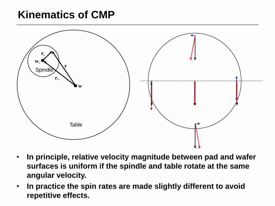
Kinematics of CMP
Table
Spindle r
w
r o
r s
w s
• In principle, relative velocity magnitude between pad and wafer
surfaces is uniform if the spindle and table rotate at the same
angular velocity.
• In practice the spin rates are made slightly different to avoid
repetitive effects.

Damascene Patterning
Two levels
Dielectric
Barrier Layer
Copper
Dielectric
Barrier Layer
Copper
Dielectric
Barrier Layer
Copper
Damascene Patterning:
• Useful for materials such as copper, which cannot be
successfully removed by conventional etching
processes.
• Requires stringent control of deposition process.
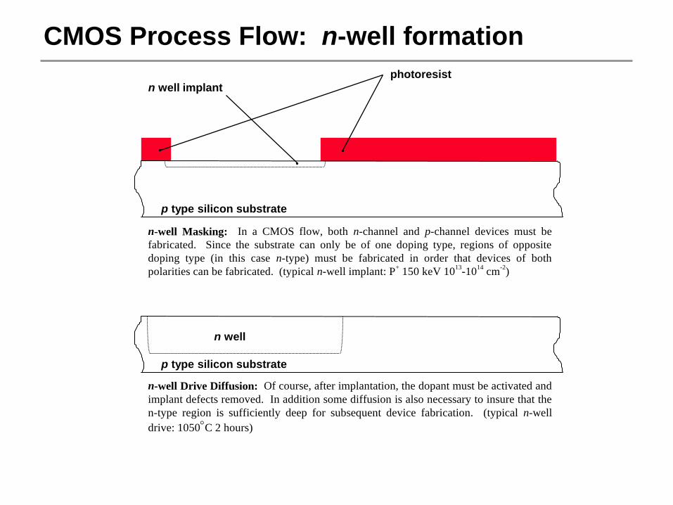
CMOS Process Flow: n-well formation
p type silicon substrate
n well
n-well Drive Diffusion: Of course, after implantation, the dopant must be activated and
implant defects removed. In addition some diffusion is also necessary to insure that the
n-type region is sufficiently deep for subsequent device fabrication. (typical n-well
drive: 1050C 2 hours)
n-well Masking: In a CMOS flow, both n-channel and p-channel devices must be
fabricated. Since the substrate can only be of one doping type, regions of opposite
doping type (in this case n-type) must be fabricated in order that devices of both
polarities can be fabricated. (typical n-well implant: P+ 150 keV 10
13-10
14 cm
-2)
p type silicon substrate
n well implant
photoresist
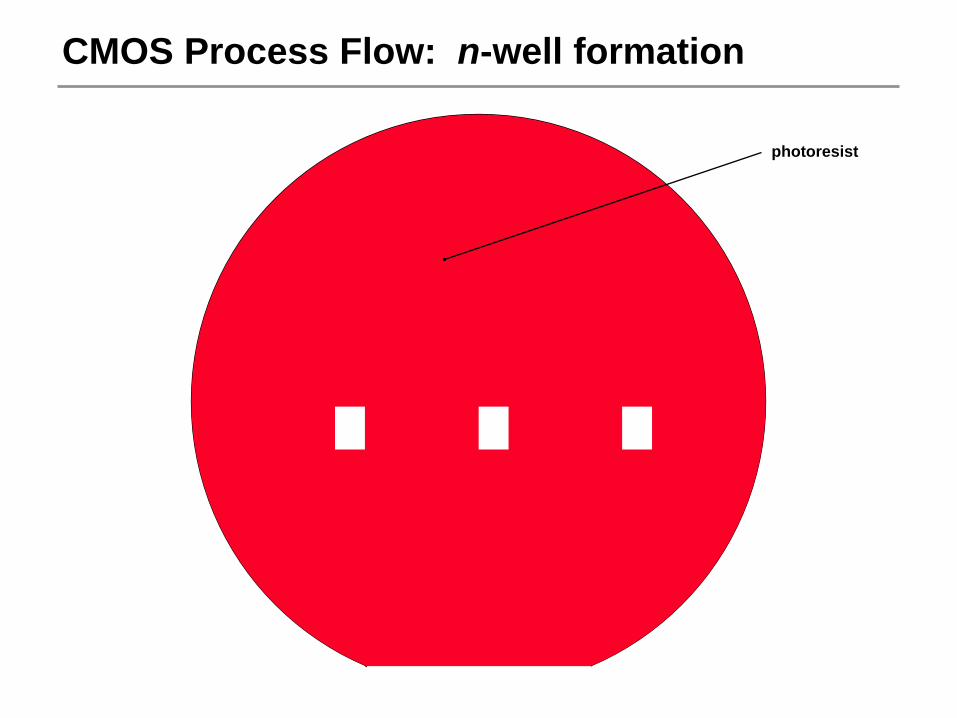
CMOS Process Flow: n-well formation
p type silicon substrate
photoresist
p type silicon substrate
n well
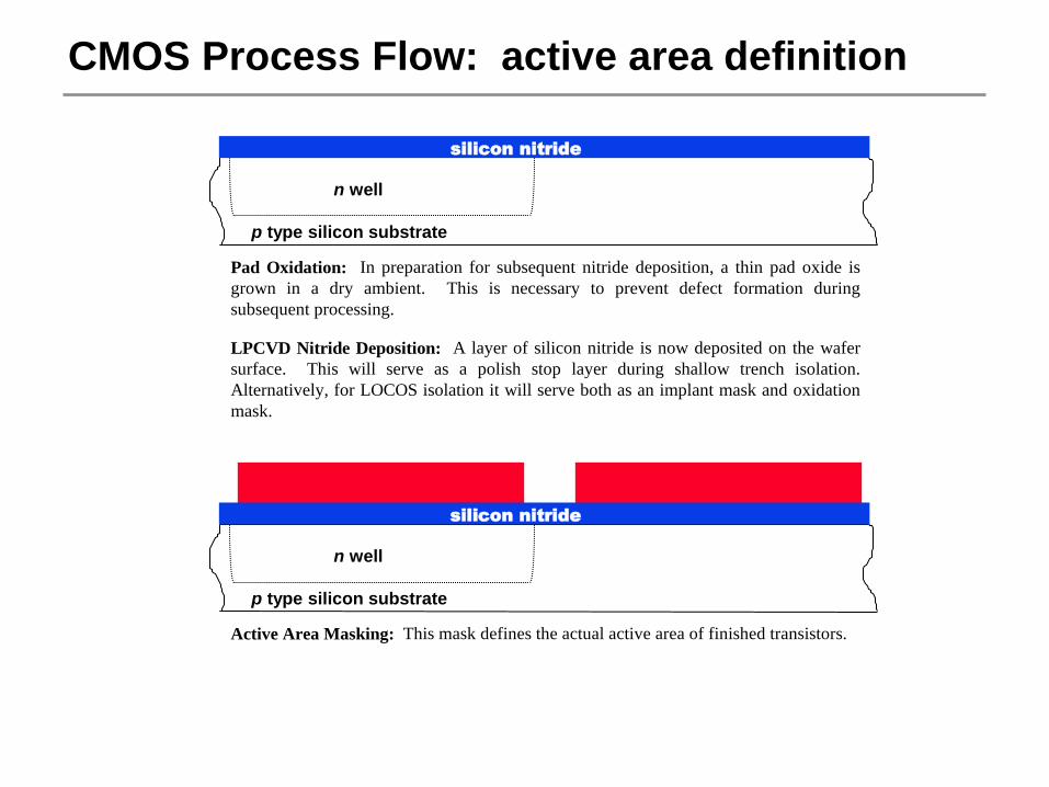
silicon nitride
Pad Oxidation: In preparation for subsequent nitride deposition, a thin pad oxide is
grown in a dry ambient. This is necessary to prevent defect formation during
subsequent processing.
LPCVD Nitride Deposition: A layer of silicon nitride is now deposited on the wafer
surface. This will serve as a polish stop layer during shallow trench isolation.
Alternatively, for LOCOS isolation it will serve both as an implant mask and oxidation
mask.
CMOS Process Flow: active area definition
p type silicon substrate
n well
silicon nitride
Active Area Masking: This mask defines the actual active area of finished transistors.

CMOS Process Flow: active area definition
CMOS Process Flow: shallow trench isolation
p type silicon substrate
n well
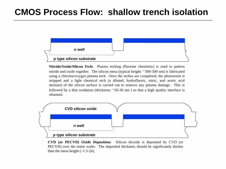
Nitride/Oxide/Silicon Etch: Plasma etching (fluorine chemistry) is used to pattern
nitride and oxide together. The silicon mesa (typical height: 300-500 nm) is fabricated
using a chlorine/oxygen plasma etch. Once the etches are completed, the photoresist is
stripped and a light chemical etch (a diluted, hydrofluoric, nitric, and acetic acid
mixture) of the silicon surface is carried out to remove any plasma damage. This is
followed by a thin oxidation (thickness: 20-30 nm ) so that a high quality interface is
obtained.
p type silicon substrate
n well
CVD (or PECVD) Oxide Deposition: Silicon dioxide is deposited by CVD (or
PECVD) over the entire wafer. The deposited thickness should be significantly thicker
than the mesa height (~1.5-2x).
CVD silicon oxide

CMOS Process Flow: shallow trench isolation
p type silicon substrate
n well
Oxide Densification: The deposited oxide generally needs to be densified since its
deposition temperature is usually low, 400C. A typical densification process is 850-
900C for 30 minutes to an hour.
Chemical Mechanical Polishing (CMP): The wafer is now polished to remove
topography due to the mesa etch. Ideally, it is desirable to remove the oxide layer to just
expose the nitride cap on top of the mesa (or alternatively, to have a polish process
which is highly selective toward oxide in comparison to nitride). In practice this is
difficult to achieve uniformly and is one of the limitations of CMP.
p type silicon substrate
n well
Nitride/Oxide Strip: The nitride and pad oxide layers are removed to expose clean
silicon.
CVD silicon oxide
CMOS Process Flow: LOCOS isolation
p type silicon substrate
n well
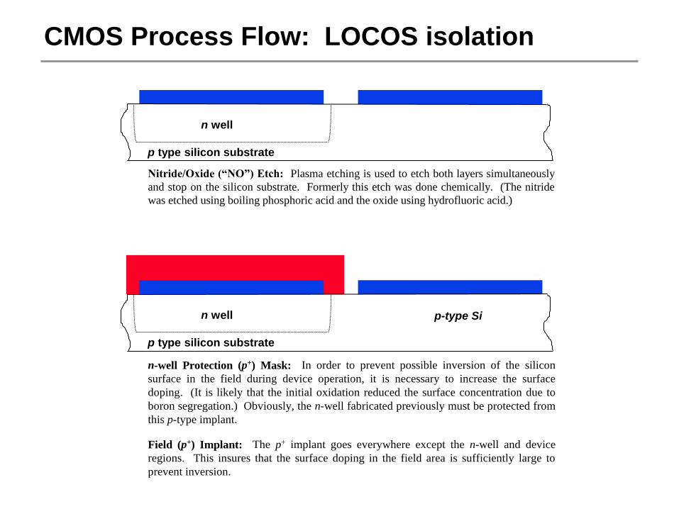
Nitride/Oxide (“NO”) Etch: Plasma etching is used to etch both layers simultaneously
and stop on the silicon substrate. Formerly this etch was done chemically. (The nitride
was etched using boiling phosphoric acid and the oxide using hydrofluoric acid.)
n-well Protection (p+) Mask: In order to prevent possible inversion of the silicon
surface in the field during device operation, it is necessary to increase the surface
doping. (It is likely that the initial oxidation reduced the surface concentration due to
boron segregation.) Obviously, the n-well fabricated previously must be protected from
this p-type implant.
Field (p+) Implant: The p+ implant goes everywhere except the n-well and device
regions. This insures that the surface doping in the field area is sufficiently large to
prevent inversion.
p type silicon substrate
n well p-type Si

p type silicon substrate
n well
LOCOS Field Oxidation: The nitride now serves as a wet oxidation mask. It is
important to control oxidation conditions so that the length of the “bird’s beak” is not
too large and that oxidation induced defects are not formed at the edge of the LOCOS
mask.
Channel Stop Mask and Implant: To insure that devices are electrically isolated, a
“channel stop” mask is defined to separate device regions. This is a high energy implant
that completely penetrates the field oxide. Again, photoresist is used as an implant mask
and must be removed after the implant.
CMOS Process Flow: LOCOS isolation
p type silicon substrate
n well
Nitride/Oxide (ONO) Strip: The nitride/oxide LOCOS mask is now stripped using
hydrofluoric acid, boiling phosphoric acid, and hydrofluoric acid again. It is necessary
to use this so-called ONO process since the nitride surface is converted to oxide during
LOCOS.

CMOS Process Flow: active area isolation
CMOS Process Flow: self-aligned source/drain
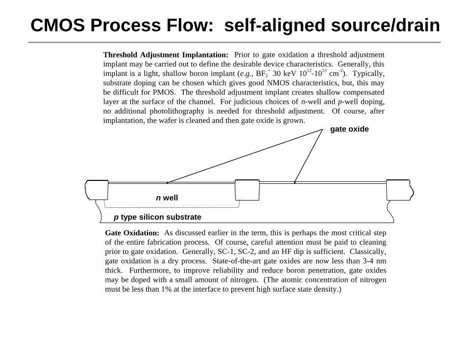
p type silicon substrate
n well
gate oxide
Gate Oxidation: As discussed earlier in the term, this is perhaps the most critical step
of the entire fabrication process. Of course, careful attention must be paid to cleaning
prior to gate oxidation. Generally, SC-1, SC-2, and an HF dip is sufficient. Classically,
gate oxidation is a dry process. State-of-the-art gate oxides are now less than 3-4 nm
thick. Furthermore, to improve reliability and reduce boron penetration, gate oxides
may be doped with a small amount of nitrogen. (The atomic concentration of nitrogen
must be less than 1% at the interface to prevent high surface state density.)
Threshold Adjustment Implantation: Prior to gate oxidation a threshold adjustment
implant may be carried out to define the desirable device characteristics. Generally, this
implant is a light, shallow boron implant (e.g., BF2+ 30 keV 10
12-10
13 cm
-2). Typically,
substrate doping can be chosen which gives good NMOS characteristics, but, this may
be difficult for PMOS. The threshold adjustment implant creates shallow compensated
layer at the surface of the channel. For judicious choices of n-well and p-well doping,
no additional photolithography is needed for threshold adjustment. Of course, after
implantation, the wafer is cleaned and then gate oxide is grown.

CMOS Process Flow: self-aligned source/drain
p type silicon substrate
n well
polysilicon
Polysilicon Deposition: A layer of polysilicon is now deposited over the entire wafer.
This polysilicon will be used to fabricate the gate electrode.
p type silicon substrate
n well
Gate Electrode Mask and Etch: The polysilicon layer is patterned using conventional
photolithography. A critical aspect of this process is the etch which must be done using
an anisotropic plasma etch with high selectivity toward the gate oxide.
CMOS Process Flow: self-aligned source/drain
p type silicon substrate
n well
n channel LDD (p-)
p type silicon substrate
n well
p channel LDD (n-)
CMOS Process Flow: self-aligned source/drain
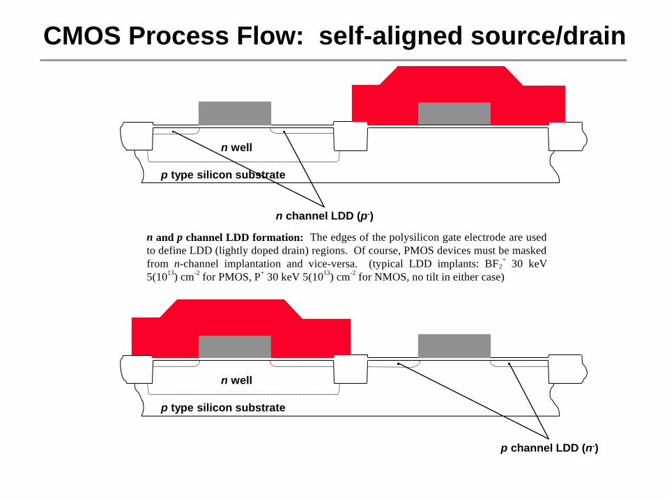
n and p channel LDD formation: The edges of the polysilicon gate electrode are used
to define LDD (lightly doped drain) regions. Of course, PMOS devices must be masked
from n-channel implantation and vice-versa. (typical LDD implants: BF2+ 30 keV
5(1013
) cm-2 for PMOS, P
+ 30 keV 5(10
13) cm
-2 for NMOS, no tilt in either case)

CMOS Process Flow: self-aligned source/drain
CMOS Process Flow: self-aligned source/drain
p type silicon substrate
n well
spacer oxide
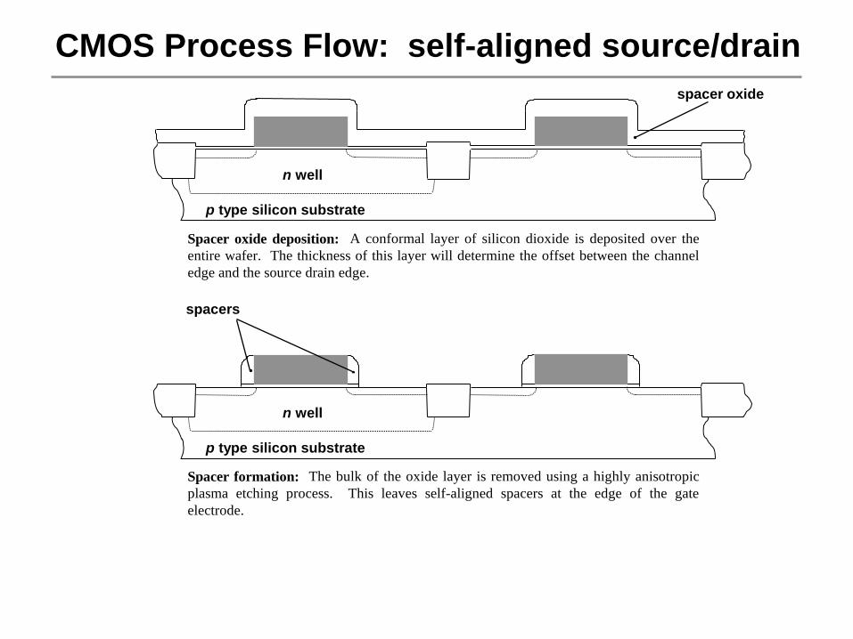
Spacer oxide deposition: A conformal layer of silicon dioxide is deposited over the
entire wafer. The thickness of this layer will determine the offset between the channel
edge and the source drain edge.
p type silicon substrate
n well
spacers
Spacer formation: The bulk of the oxide layer is removed using a highly anisotropic
plasma etching process. This leaves self-aligned spacers at the edge of the gate
electrode.
p type silicon substrate
n well
n channel source/drain (p+)
p type silicon substrate
n well
p channel source/drain (n+)
CMOS Process Flow: self-aligned source/drain
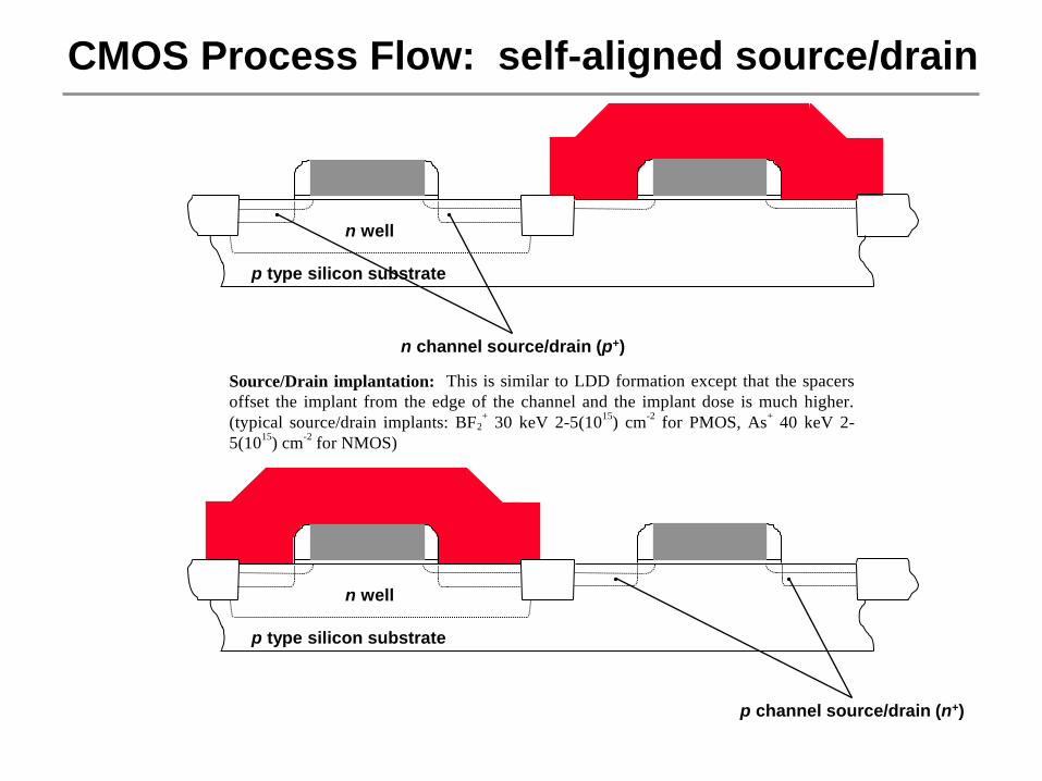
Source/Drain implantation: This is similar to LDD formation except that the spacers
offset the implant from the edge of the channel and the implant dose is much higher.
(typical source/drain implants: BF2+ 30 keV 2-5(10
15) cm
-2 for PMOS, As
+ 40 keV 2-
5(1015
) cm-2 for NMOS)

CMOS Process Flow: self-aligned source/drain
CMOS Process Flow: self-aligned source/drain
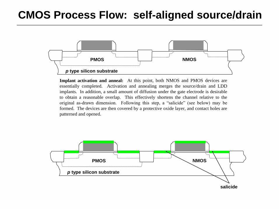
Implant activation and anneal: At this point, both NMOS and PMOS devices are
essentially completed. Activation and annealing merges the source/drain and LDD
implants. In addition, a small amount of diffusion under the gate electrode is desirable
to obtain a reasonable overlap. This effectively shortens the channel relative to the
original as-drawn dimension. Following this step, a “salicide” (see below) may be
formed. The devices are then covered by a protective oxide layer, and contact holes are
patterned and opened.
p type silicon substrate
PMOS NMOS
p type silicon substrate
PMOS NMOS
salicide
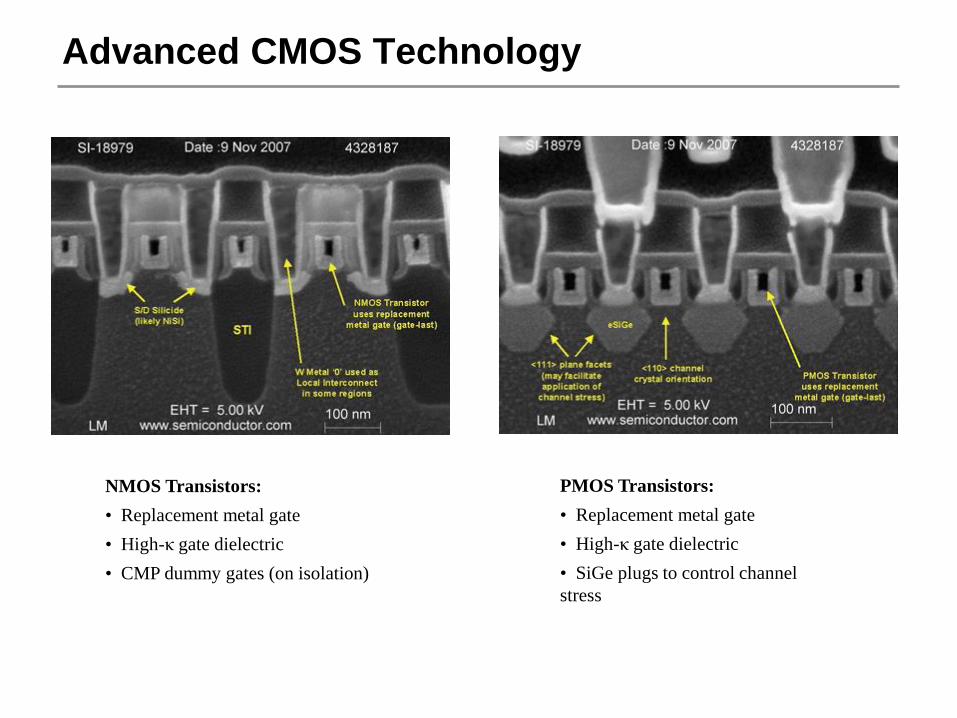
Advanced CMOS Technology
NMOS Transistors:
• Replacement metal gate
• High-κ gate dielectric
• CMP dummy gates (on isolation)
PMOS Transistors:
• Replacement metal gate
• High-κ gate dielectric
• SiGe plugs to control channel
stress

Advanced CMOS Technology

Tri-gate (FinFET)
Tri-gate Transistors:
Represent a truly
revolutionary departure from
conventional MOSFET
technology

Intel Transistor Innovations
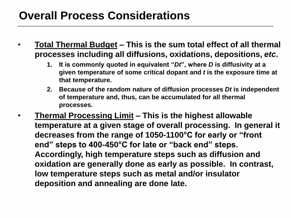
Overall Process Considerations
• Total Thermal Budget – This is the sum total effect of all thermal
processes including all diffusions, oxidations, depositions, etc.
1. It is commonly quoted in equivalent “Dt”, where D is diffusivity at a
given temperature of some critical dopant and t is the exposure time at
that temperature.
2. Because of the random nature of diffusion processes Dt is independent
of temperature and, thus, can be accumulated for all thermal
processes.
• Thermal Processing Limit – This is the highest allowable
temperature at a given stage of overall processing. In general it
decreases from the range of 1050-1100°C for early or “front
end” steps to 400-450°C for late or “back end” steps.
Accordingly, high temperature steps such as diffusion and
oxidation are generally done as early as possible. In contrast,
low temperature steps such as metal and/or insulator
deposition and annealing are done late.

Process Control
• Statistical Methods (SPC) – Pioneered by Walter A. Shewhart
and taken up by W. Edwards Deming after the Second World
War.
• Response Parameters – Objectively measurable quantities well-
correlated with the process.
1. Sheet resistance
2. Thin film thickness
3. Others
• Control Parameters – Adjustable parameters that cause a
change in response.
1. Time.
2. Temperature
3. Chemical concentration (e.g., implant dose)
4. Others
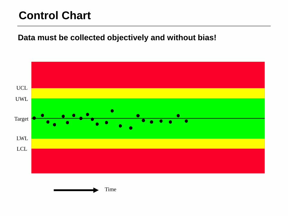
Control Chart
Data must be collected objectively and without bias!
Time
Target
UWL
UCL
LWL
LCL