intel® 64 and ia-32 architectures software developer’s...
TRANSCRIPT

Intel® 64 and IA-32 ArchitecturesSoftware Developer’s Manual
Volume 3A:System Programming Guide, Part 1
NOTE: The Intel® 64 and IA-32 Architectures Software Developer's Manualconsists of five volumes: Basic Architecture, Order Number 253665;Instruction Set Reference A-M, Order Number 253666; Instruction SetReference N-Z, Order Number 253667; System Programming Guide,Part 1, Order Number 253668; System Programming Guide, Part 2, OrderNumber 253669. Refer to all five volumes when evaluating your designneeds.
Order Number: 253668-034USMarch 2010

CHAPTER 1ABOUT THIS MANUAL
The Intel® 64 and IA-32 Architectures Software Developer’s Manual, Volume 3A: System Programming Guide, Part 1 (order number 253668) and the Intel® 64 and IA-32 Architectures Software Developer’s Manual, Volume 3B: System Programming Guide, Part 2 (order number 253669) are part of a set that describes the architecture and programming environment of Intel 64 and IA-32 Architecture processors. The other volumes in this set are:
• Intel® 64 and IA-32 Architectures Software Developer’s Manual, Volume 1: Basic Architecture (order number 253665).
• Intel® 64 and IA-32 Architectures Software Developer’s Manual, Volumes 2A & 2B: Instruction Set Reference (order numbers 253666 and 253667).
The Intel® 64 and IA-32 Architectures Software Developer’s Manual, Volume 1, describes the basic architecture and programming environment of Intel 64 and IA-32 processors. The Intel® 64 and IA-32 Architectures Software Developer’s Manual, Volumes 2A & 2B, describe the instruction set of the processor and the opcode struc-ture. These volumes apply to application programmers and to programmers who write operating systems or executives. The Intel® 64 and IA-32 Architectures Soft-ware Developer’s Manual, Volumes 3A & 3B, describe the operating-system support environment of Intel 64 and IA-32 processors. These volumes target operating-system and BIOS designers. In addition, Intel® 64 and IA-32 Architectures Software Developer’s Manual, Volume 3B, addresses the programming environment for classes of software that host operating systems.
1.1 PROCESSORS COVERED IN THIS MANUALThis manual set includes information pertaining primarily to the most recent Intel® 64 and IA-32 processors, which include:
• Pentium® processors
• P6 family processors
• Pentium® 4 processors
• Pentium® M processors
• Intel® Xeon® processors
• Pentium® D processors
• Pentium® processor Extreme Editions
• 64-bit Intel® Xeon® processors
• Intel® Core™ Duo processor
• Intel® Core™ Solo processor
Vol. 3 1-1

ABOUT THIS MANUAL
• Dual-Core Intel® Xeon® processor LV
• Intel® Core™2 Duo processor
• Intel® Core™2 Quad processor Q6000 series
• Intel® Xeon® processor 3000, 3200 series
• Intel® Xeon® processor 5000 series
• Intel® Xeon® processor 5100, 5300 series
• Intel® Core™2 Extreme processor X7000 and X6800 series
• Intel® Core™2 Extreme QX6000 series
• Intel® Xeon® processor 7100 series
• Intel® Pentium® Dual-Core processor
• Intel® Xeon® processor 7200, 7300 series
• Intel® Core™2 Extreme QX9000 series
• Intel® Xeon® processor 5200, 5400, 7400 series
• Intel® CoreTM2 Extreme processor QX9000 and X9000 series
• Intel® CoreTM2 Quad processor Q9000 series
• Intel® CoreTM2 Duo processor E8000, T9000 series
• Intel® AtomTM processor family
• Intel® CoreTM i7 processor
• Intel® CoreTM i5 processor
P6 family processors are IA-32 processors based on the P6 family microarchitecture. This includes the Pentium® Pro, Pentium® II, Pentium® III, and Pentium® III Xeon® processors.
The Pentium® 4, Pentium® D, and Pentium® processor Extreme Editions are based on the Intel NetBurst® microarchitecture. Most early Intel® Xeon® processors are based on the Intel NetBurst® microarchitecture. Intel Xeon processor 5000, 7100 series are based on the Intel NetBurst® microarchitecture.
The Intel® Core™ Duo, Intel® Core™ Solo and dual-core Intel® Xeon® processor LV are based on an improved Pentium® M processor microarchitecture.
The Intel® Xeon® processor 3000, 3200, 5100, 5300, 7200, and 7300 series, Intel® Pentium® dual-core, Intel® Core™2 Duo, Intel® Core™2 Quad and Intel® Core™2 Extreme processors are based on Intel® Core™ microarchitecture.
The Intel® Xeon® processor 5200, 5400, 7400 series, Intel® CoreTM2 Quad processor Q9000 series, and Intel® CoreTM2 Extreme processors QX9000, X9000 series, Intel® CoreTM2 processor E8000 series are based on Enhanced Intel® CoreTM microarchitec-ture.
The Intel® AtomTM processor family is based on the Intel® AtomTM microarchitecture and supports Intel 64 architecture.
1-2 Vol. 3

ABOUT THIS MANUAL
The Intel® CoreTM i7 processor and the Intel® CoreTM i5 processor are based on the Intel® microarchitecture codename Nehalem and support Intel 64 architecture.
Processors based on the Next Generation Intel Processor, codenamed Westmere, support Intel 64 architecture.
P6 family, Pentium® M, Intel® Core™ Solo, Intel® Core™ Duo processors, dual-core Intel® Xeon® processor LV, and early generations of Pentium 4 and Intel Xeon processors support IA-32 architecture. The Intel® Atom™ processor Z5xx series support IA-32 architecture.
The Intel® Xeon® processor 3000, 3200, 5000, 5100, 5200, 5300, 5400, 7100, 7200, 7300, 7400 series, Intel® Core™2 Duo, Intel® Core™2 Extreme processors, Intel Core 2 Quad processors, Pentium® D processors, Pentium® Dual-Core processor, newer generations of Pentium 4 and Intel Xeon processor family support Intel® 64 architecture.
IA-32 architecture is the instruction set architecture and programming environment for Intel's 32-bit microprocessors. Intel® 64 architecture is the instruction set archi-tecture and programming environment which is a superset of and compatible with IA-32 architecture.
1.2 OVERVIEW OF THE SYSTEM PROGRAMMING GUIDEA description of this manual’s content follows:
Chapter 1 — About This Manual. Gives an overview of all five volumes of the Intel® 64 and IA-32 Architectures Software Developer’s Manual. It also describes the notational conventions in these manuals and lists related Intel manuals and documentation of interest to programmers and hardware designers.
Chapter 2 — System Architecture Overview. Describes the modes of operation used by Intel 64 and IA-32 processors and the mechanisms provided by the architec-tures to support operating systems and executives, including the system-oriented registers and data structures and the system-oriented instructions. The steps neces-sary for switching between real-address and protected modes are also identified.
Chapter 3 — Protected-Mode Memory Management. Describes the data struc-tures, registers, and instructions that support segmentation and paging. The chapter explains how they can be used to implement a “flat” (unsegmented) memory model or a segmented memory model.
Chapter 4 — Paging. Describes the paging modes supported by Intel 64 and IA-32 processors.
Chapter 5 — Protection. Describes the support for page and segment protection provided in the Intel 64 and IA-32 architectures. This chapter also explains the implementation of privilege rules, stack switching, pointer validation, user and supervisor modes.
Vol. 3 1-3

ABOUT THIS MANUAL
Chapter 6 — Interrupt and Exception Handling. Describes the basic interrupt mechanisms defined in the Intel 64 and IA-32 architectures, shows how interrupts and exceptions relate to protection, and describes how the architecture handles each exception type. Reference information for each exception is given at the end of this chapter.
Chapter 7 — Task Management. Describes mechanisms the Intel 64 and IA-32 architectures provide to support multitasking and inter-task protection.
Chapter 8 — Multiple-Processor Management. Describes the instructions and flags that support multiple processors with shared memory, memory ordering, and Intel® Hyper-Threading Technology.
Chapter 9 — Processor Management and Initialization. Defines the state of an Intel 64 or IA-32 processor after reset initialization. This chapter also explains how to set up an Intel 64 or IA-32 processor for real-address mode operation and protected- mode operation, and how to switch between modes.
Chapter 10 — Advanced Programmable Interrupt Controller (APIC). Describes the programming interface to the local APIC and gives an overview of the interface between the local APIC and the I/O APIC.
Chapter 11 — Memory Cache Control. Describes the general concept of caching and the caching mechanisms supported by the Intel 64 or IA-32 architectures. This chapter also describes the memory type range registers (MTRRs) and how they can be used to map memory types of physical memory. Information on using the new cache control and memory streaming instructions introduced with the Pentium III, Pentium 4, and Intel Xeon processors is also given.
Chapter 12 — Intel® MMX™ Technology System Programming. Describes those aspects of the Intel® MMX™ technology that must be handled and considered at the system programming level, including: task switching, exception handling, and compatibility with existing system environments.
Chapter 13 — System Programming For Instruction Set Extensions And Processor Extended States. Describes the operating system requirements to support SSE/SSE2/SSE3/SSSE3/SSE4 extensions, including task switching, excep-tion handling, and compatibility with existing system environments. The latter part of this chapter describes the extensible framework of operating system requirements to support processor extended states. Processor extended state may be required by instruction set extensions beyond those of SSE/SSE2/SSE3/SSSE3/SSE4 extensions.
Chapter 14 — Power and Thermal Management. Describes facilities of Intel 64 and IA-32 architecture used for power management and thermal monitoring.
Chapter 15 — Machine-Check Architecture. Describes the machine-check architecture and machine-check exception mechanism found in the Pentium 4, Intel Xeon, and P6 family processors. Additionally, a signaling mechanism for software to respond to hardware corrected machine check error is covered.
1-4 Vol. 3

ABOUT THIS MANUAL
Chapter 16 — Debugging, Branch Profiles and Time-Stamp Counter. Describes the debugging registers and other debug mechanism provided in Intel 64 or IA-32 processors. This chapter also describes the time-stamp counter.
Chapter 17 — 8086 Emulation. Describes the real-address and virtual-8086 modes of the IA-32 architecture.
Chapter 18 — Mixing 16-Bit and 32-Bit Code. Describes how to mix 16-bit and 32-bit code modules within the same program or task.
Chapter 19 — IA-32 Architecture Compatibility. Describes architectural compatibility among IA-32 processors.
Chapter 20 — Introduction to Virtual-Machine Extensions. Describes the basic elements of virtual machine architecture and the virtual-machine extensions for Intel 64 and IA-32 Architectures.
Chapter 21 — Virtual-Machine Control Structures. Describes components that manage VMX operation. These include the working-VMCS pointer and the control-ling-VMCS pointer.
Chapter 22— VMX Non-Root Operation. Describes the operation of a VMX non-root operation. Processor operation in VMX non-root mode can be restricted programmatically such that certain operations, events or conditions can cause the processor to transfer control from the guest (running in VMX non-root mode) to the monitor software (running in VMX root mode).
Chapter 23 — VM Entries. Describes VM entries. VM entry transitions the processor from the VMM running in VMX root-mode to a VM running in VMX non-root mode. VM-Entry is performed by the execution of VMLAUNCH or VMRESUME instructions.
Chapter 24 — VM Exits. Describes VM exits. Certain events, operations or situa-tions while the processor is in VMX non-root operation may cause VM-exit transitions. In addition, VM exits can also occur on failed VM entries.
Chapter 25 — VMX Support for Address Translation. Describes virtual-machine extensions that support address translation and the virtualization of physical memory.
Chapter 26 — System Management Mode. Describes Intel 64 and IA-32 architec-tures’ system management mode (SMM) facilities.
Chapter 27 — Virtual-Machine Monitoring Programming Considerations. Describes programming considerations for VMMs. VMMs manage virtual machines (VMs).
Chapter 28 — Virtualization of System Resources. Describes the virtualization of the system resources. These include: debugging facilities, address translation, physical memory, and microcode update facilities.
Chapter 29 — Handling Boundary Conditions in a Virtual Machine Monitor. Describes what a VMM must consider when handling exceptions, interrupts, error conditions, and transitions between activity states.
Vol. 3 1-5

ABOUT THIS MANUAL
Chapter 30 — Performance Monitoring. Describes the Intel 64 and IA-32 archi-tectures’ facilities for monitoring performance.
Appendix A — Performance-Monitoring Events. Lists architectural performance events. Non-architectural performance events (i.e. model-specific events) are listed for each generation of microarchitecture.
Appendix B — Model-Specific Registers (MSRs). Lists the MSRs available in the Pentium processors, the P6 family processors, the Pentium 4, Intel Xeon, Intel Core Solo, Intel Core Duo processors, and Intel Core 2 processor family and describes their functions.
Appendix C — MP Initialization For P6 Family Processors. Gives an example of how to use of the MP protocol to boot P6 family processors in n MP system.
Appendix D — Programming the LINT0 and LINT1 Inputs. Gives an example of how to program the LINT0 and LINT1 pins for specific interrupt vectors.
Appendix E — Interpreting Machine-Check Error Codes. Gives an example of how to interpret the error codes for a machine-check error that occurred on a P6 family processor.
Appendix F — APIC Bus Message Formats. Describes the message formats for messages transmitted on the APIC bus for P6 family and Pentium processors.
Appendix G — VMX Capability Reporting Facility. Describes the VMX capability MSRs. Support for specific VMX features is determined by reading capability MSRs.
Appendix H — Field Encoding in VMCS. Enumerates all fields in the VMCS and their encodings. Fields are grouped by width (16-bit, 32-bit, etc.) and type (guest-state, host-state, etc.).
Appendix I — VM Basic Exit Reasons. Describes the 32-bit fields that encode reasons for a VM exit. Examples of exit reasons include, but are not limited to: soft-ware interrupts, processor exceptions, software traps, NMIs, external interrupts, and triple faults.
1.3 NOTATIONAL CONVENTIONSThis manual uses specific notation for data-structure formats, for symbolic represen-tation of instructions, and for hexadecimal and binary numbers. A review of this notation makes the manual easier to read.
1.3.1 Bit and Byte OrderIn illustrations of data structures in memory, smaller addresses appear toward the bottom of the figure; addresses increase toward the top. Bit positions are numbered from right to left. The numerical value of a set bit is equal to two raised to the power of the bit position. Intel 64 and IA-32 processors are “little endian” machines; this
1-6 Vol. 3

ABOUT THIS MANUAL
means the bytes of a word are numbered starting from the least significant byte. Figure 1-1 illustrates these conventions.
1.3.2 Reserved Bits and Software CompatibilityIn many register and memory layout descriptions, certain bits are marked as reserved. When bits are marked as reserved, it is essential for compatibility with future processors that software treat these bits as having a future, though unknown, effect. The behavior of reserved bits should be regarded as not only undefined, but unpredictable. Software should follow these guidelines in dealing with reserved bits:
• Do not depend on the states of any reserved bits when testing the values of registers which contain such bits. Mask out the reserved bits before testing.
• Do not depend on the states of any reserved bits when storing to memory or to a register.
• Do not depend on the ability to retain information written into any reserved bits.
• When loading a register, always load the reserved bits with the values indicated in the documentation, if any, or reload them with values previously read from the same register.
NOTEAvoid any software dependence upon the state of reserved bits in Intel 64 and IA-32 registers. Depending upon the values of reserved register bits will make software dependent upon the unspecified manner in which the processor handles these bits. Programs that depend upon reserved values risk incompatibility with future processors.
Figure 1-1. Bit and Byte Order
Byte 3
HighestData Structure
Byte 1Byte 2 Byte 0
31 24 23 16 15 8 7 0Address
Lowest
Bit offset2824201612840 Address
Byte Offset
Vol. 3 1-7

ABOUT THIS MANUAL
1.3.3 Instruction OperandsWhen instructions are represented symbolically, a subset of assembly language is used. In this subset, an instruction has the following format:
label: mnemonic argument1, argument2, argument3
where:
• A label is an identifier which is followed by a colon.
• A mnemonic is a reserved name for a class of instruction opcodes which have the same function.
• The operands argument1, argument2, and argument3 are optional. There may be from zero to three operands, depending on the opcode. When present, they take the form of either literals or identifiers for data items. Operand identifiers are either reserved names of registers or are assumed to be assigned to data items declared in another part of the program (which may not be shown in the example).
When two operands are present in an arithmetic or logical instruction, the right operand is the source and the left operand is the destination.
For example:
LOADREG: MOV EAX, SUBTOTAL
In this example LOADREG is a label, MOV is the mnemonic identifier of an opcode, EAX is the destination operand, and SUBTOTAL is the source operand. Some assembly languages put the source and destination in reverse order.
1.3.4 Hexadecimal and Binary NumbersBase 16 (hexadecimal) numbers are represented by a string of hexadecimal digits followed by the character H (for example, F82EH). A hexadecimal digit is a character from the following set: 0, 1, 2, 3, 4, 5, 6, 7, 8, 9, A, B, C, D, E, and F.
Base 2 (binary) numbers are represented by a string of 1s and 0s, sometimes followed by the character B (for example, 1010B). The “B” designation is only used in situations where confusion as to the type of number might arise.
1.3.5 Segmented AddressingThe processor uses byte addressing. This means memory is organized and accessed as a sequence of bytes. Whether one or more bytes are being accessed, a byte address is used to locate the byte or bytes memory. The range of memory that can be addressed is called an address space.
The processor also supports segmented addressing. This is a form of addressing where a program may have many independent address spaces, called segments.
1-8 Vol. 3

ABOUT THIS MANUAL
For example, a program can keep its code (instructions) and stack in separate segments. Code addresses would always refer to the code space, and stack addresses would always refer to the stack space. The following notation is used to specify a byte address within a segment:
Segment-register:Byte-address
For example, the following segment address identifies the byte at address FF79H in the segment pointed by the DS register:
DS:FF79H
The following segment address identifies an instruction address in the code segment. The CS register points to the code segment and the EIP register contains the address of the instruction.
CS:EIP
1.3.6 Syntax for CPUID, CR, and MSR ValuesObtain feature flags, status, and system information by using the CPUID instruction, by checking control register bits, and by reading model-specific registers. We are moving toward a single syntax to represent this type of information. See Figure 1-2.
Vol. 3 1-9

CHAPTER 2SYSTEM ARCHITECTURE OVERVIEW
IA-32 architecture (beginning with the Intel386 processor family) provides extensive support for operating-system and system-development software. This support offers multiple modes of operation, which include:
• Real mode, protected mode, virtual 8086 mode, and system management mode. These are sometimes referred to as legacy modes.
Intel 64 architecture supports almost all the system programming facilities available in IA-32 architecture and extends them to a new operating mode (IA-32e mode) that supports a 64-bit programming environment. IA-32e mode allows software to operate in one of two sub-modes:
• 64-bit mode supports 64-bit OS and 64-bit applications
• Compatibility mode allows most legacy software to run; it co-exists with 64-bit applications under a 64-bit OS.
The IA-32 system-level architecture and includes features to assist in the following operations:
• Memory management
• Protection of software modules
• Multitasking
• Exception and interrupt handling
• Multiprocessing
• Cache management
• Hardware resource and power management
• Debugging and performance monitoring
This chapter provides a description of each part of this architecture. It also describes the system registers that are used to set up and control the processor at the system level and gives a brief overview of the processor’s system-level (operating system) instructions.
Many features of the system-level architectural are used only by system program-mers. However, application programmers may need to read this chapter and the following chapters in order to create a reliable and secure environment for applica-tion programs.
This overview and most subsequent chapters of this book focus on protected-mode operation of the IA-32 architecture. IA-32e mode operation of the Intel 64 architec-ture, as it differs from protected mode operation, is also described.
All Intel 64 and IA-32 processors enter real-address mode following a power-up or reset (see Chapter 9, “Processor Management and Initialization”). Software then
Vol. 3 2-1

SYSTEM ARCHITECTURE OVERVIEW
initiates the switch from real-address mode to protected mode. If IA-32e mode oper-ation is desired, software also initiates a switch from protected mode to IA-32e mode.
2.1 OVERVIEW OF THE SYSTEM-LEVEL ARCHITECTURESystem-level architecture consists of a set of registers, data structures, and instruc-tions designed to support basic system-level operations such as memory manage-ment, interrupt and exception handling, task management, and control of multiple processors.
Figure 2-1 provides a summary of system registers and data structures that applies to 32-bit modes. System registers and data structures that apply to IA-32e mode are shown in Figure 2-2.
2-2 Vol. 3

SYSTEM ARCHITECTURE OVERVIEW
Figure 2-1. IA-32 System-Level Registers and Data Structures
Local DescriptorTable (LDT)
EFLAGS Register
Control Registers
CR1CR2CR3CR4
CR0 Global DescriptorTable (GDT)
Interrupt DescriptorTable (IDT)
IDTR
GDTR
Interrupt Gate
Trap Gate
LDT Desc.
TSS Desc.
CodeStack
CodeStack
CodeStack
Task-StateSegment (TSS)
CodeData
Stack
Task
Interrupt Handler
Exception Handler
Protected Procedure
TSS Seg. Sel.
Call-GateSegment Selector
Dir Table OffsetLinear Address
Page Directory
Pg. Dir. Entry
Linear Address Space
Linear Addr.
0
Seg. Desc.Segment Sel.
Code, Data orStack Segment
InterruptVector
TSS Desc.
Seg. Desc.
Task Gate
CurrentTSS
Call Gate
Task-StateSegment (TSS)
CodeData
Stack
Task
Seg. Desc.
CurrentTSS
CurrentTSS
Segment Selector
Linear Address
Task Register
CR3*
Page Table
Pg. Tbl. Entry
Page
Physical Addr.
LDTR
This page mapping example is for 4-KByte pagesand the normal 32-bit physical address size.
Register
*Physical Address
Physical Address
XCR0 (XFEM)
Vol. 3 2-3

SYSTEM ARCHITECTURE OVERVIEW
Figure 2-2. System-Level Registers and Data Structures in IA-32e Mode
Local DescriptorTable (LDT)
CR1CR2CR3CR4
CR0 Global DescriptorTable (GDT)
Interrupt DescriptorTable (IDT)
IDTR
GDTR
Interrupt Gate
Trap Gate
LDT Desc.
TSS Desc.
CodeStack
CodeStack
CodeStack
Current TSSCode
Stack
Interr. Handler
Interrupt Handler
Exception Handler
Protected Procedure
TR
Call-GateSegment Selector
Linear Address
PML4
PML4.
Linear Address Space
Linear Addr.
0
Seg. Desc.Segment Sel.
Code, Data or Stack Segment (Base =0)
InterruptVector
Seg. Desc.
Seg. Desc.
NULL
Call Gate
Task-StateSegment (TSS)
Seg. Desc.
NULL
NULL
Segment Selector
Linear Address
Task Register
CR3*
Page
LDTR
This page mapping example is for 4-KByte pagesand 40-bit physical address size.
Register
*Physical Address
Physical Address
CR8Control Register
RFLAGS
OffsetTableDirectory
Page Table
Entry
PhysicalAddr.Page Tbl
Entry
Page Dir.Pg. Dir. Ptr.
PML4 Dir. Pointer
Pg. Dir.Entry
Interrupt GateIST
XCR0 (XFEM)
2-4 Vol. 3

SYSTEM ARCHITECTURE OVERVIEW
2.1.1 Global and Local Descriptor TablesWhen operating in protected mode, all memory accesses pass through either the global descriptor table (GDT) or an optional local descriptor table (LDT) as shown in Figure 2-1. These tables contain entries called segment descriptors. Segment descriptors provide the base address of segments well as access rights, type, and usage information.
Each segment descriptor has an associated segment selector. A segment selector provides the software that uses it with an index into the GDT or LDT (the offset of its associated segment descriptor), a global/local flag (determines whether the selector points to the GDT or the LDT), and access rights information.
To access a byte in a segment, a segment selector and an offset must be supplied. The segment selector provides access to the segment descriptor for the segment (in the GDT or LDT). From the segment descriptor, the processor obtains the base address of the segment in the linear address space. The offset then provides the location of the byte relative to the base address. This mechanism can be used to access any valid code, data, or stack segment, provided the segment is accessible from the current privilege level (CPL) at which the processor is operating. The CPL is defined as the protection level of the currently executing code segment.
See Figure 2-1. The solid arrows in the figure indicate a linear address, dashed lines indicate a segment selector, and the dotted arrows indicate a physical address. For simplicity, many of the segment selectors are shown as direct pointers to a segment. However, the actual path from a segment selector to its associated segment is always through a GDT or LDT.
The linear address of the base of the GDT is contained in the GDT register (GDTR); the linear address of the LDT is contained in the LDT register (LDTR).
2.1.1.1 Global and Local Descriptor Tables in IA-32e ModeGDTR and LDTR registers are expanded to 64-bits wide in both IA-32e sub-modes (64-bit mode and compatibility mode). For more information: see Section 3.5.2, “Segment Descriptor Tables in IA-32e Mode.”
Global and local descriptor tables are expanded in 64-bit mode to support 64-bit base addresses, (16-byte LDT descriptors hold a 64-bit base address and various attributes). In compatibility mode, descriptors are not expanded.
2.1.2 System Segments, Segment Descriptors, and GatesBesides code, data, and stack segments that make up the execution environment of a program or procedure, the architecture defines two system segments: the task-state segment (TSS) and the LDT. The GDT is not considered a segment because it is not accessed by means of a segment selector and segment descriptor. TSSs and LDTs have segment descriptors defined for them.
Vol. 3 2-5
SYSTEM ARCHITECTURE OVERVIEW
The architecture also defines a set of special descriptors called gates (call gates, interrupt gates, trap gates, and task gates). These provide protected gateways to system procedures and handlers that may operate at a different privilege level than application programs and most procedures. For example, a CALL to a call gate can provide access to a procedure in a code segment that is at the same or a numerically lower privilege level (more privileged) than the current code segment. To access a procedure through a call gate, the calling procedure1 supplies the selector for the call gate. The processor then performs an access rights check on the call gate, comparing the CPL with the privilege level of the call gate and the destination code segment pointed to by the call gate.
If access to the destination code segment is allowed, the processor gets the segment selector for the destination code segment and an offset into that code segment from the call gate. If the call requires a change in privilege level, the processor also switches to the stack for the targeted privilege level. The segment selector for the new stack is obtained from the TSS for the currently running task. Gates also facili-tate transitions between 16-bit and 32-bit code segments, and vice versa.
2.1.2.1 Gates in IA-32e ModeIn IA-32e mode, the following descriptors are 16-byte descriptors (expanded to allow a 64-bit base): LDT descriptors, 64-bit TSSs, call gates, interrupt gates, and trap gates.
Call gates facilitate transitions between 64-bit mode and compatibility mode. Task gates are not supported in IA-32e mode. On privilege level changes, stack segment selectors are not read from the TSS. Instead, they are set to NULL.
2.1.3 Task-State Segments and Task GatesThe TSS (see Figure 2-1) defines the state of the execution environment for a task. It includes the state of general-purpose registers, segment registers, the EFLAGS register, the EIP register, and segment selectors with stack pointers for three stack segments (one stack for each privilege level). The TSS also includes the segment selector for the LDT associated with the task and the base address of the paging-structure hierarchy.
All program execution in protected mode happens within the context of a task (called the current task). The segment selector for the TSS for the current task is stored in the task register. The simplest method for switching to a task is to make a call or jump to the new task. Here, the segment selector for the TSS of the new task is given in the CALL or JMP instruction. In switching tasks, the processor performs the following actions:
1. Stores the state of the current task in the current TSS.
1. The word “procedure” is commonly used in this document as a general term for a logical unit or block of code (such as a program, procedure, function, or routine).
2-6 Vol. 3
SYSTEM ARCHITECTURE OVERVIEW
2. Loads the task register with the segment selector for the new task.
3. Accesses the new TSS through a segment descriptor in the GDT.
4. Loads the state of the new task from the new TSS into the general-purpose registers, the segment registers, the LDTR, control register CR3 (base address of the paging-structure hierarchy), the EFLAGS register, and the EIP register.
5. Begins execution of the new task.
A task can also be accessed through a task gate. A task gate is similar to a call gate, except that it provides access (through a segment selector) to a TSS rather than a code segment.
2.1.3.1 Task-State Segments in IA-32e ModeHardware task switches are not supported in IA-32e mode. However, TSSs continue to exist. The base address of a TSS is specified by its descriptor.
A 64-bit TSS holds the following information that is important to 64-bit operation:
• Stack pointer addresses for each privilege level
• Pointer addresses for the interrupt stack table
• Offset address of the IO-permission bitmap (from the TSS base)
The task register is expanded to hold 64-bit base addresses in IA-32e mode. See also: Section 7.7, “Task Management in 64-bit Mode.”
2.1.4 Interrupt and Exception HandlingExternal interrupts, software interrupts and exceptions are handled through the interrupt descriptor table (IDT). The IDT stores a collection of gate descriptors that provide access to interrupt and exception handlers. Like the GDT, the IDT is not a segment. The linear address for the base of the IDT is contained in the IDT register (IDTR).
Gate descriptors in the IDT can be interrupt, trap, or task gate descriptors. To access an interrupt or exception handler, the processor first receives an interrupt vector (interrupt number) from internal hardware, an external interrupt controller, or from software by means of an INT, INTO, INT 3, or BOUND instruction. The interrupt vector provides an index into the IDT. If the selected gate descriptor is an interrupt gate or a trap gate, the associated handler procedure is accessed in a manner similar to calling a procedure through a call gate. If the descriptor is a task gate, the handler is accessed through a task switch.
2.1.4.1 Interrupt and Exception Handling IA-32e ModeIn IA-32e mode, interrupt descriptors are expanded to 16 bytes to support 64-bit base addresses. This is true for 64-bit mode and compatibility mode.
Vol. 3 2-7

SYSTEM ARCHITECTURE OVERVIEW
The IDTR register is expanded to hold a 64-bit base address. Task gates are not supported.
2.1.5 Memory ManagementSystem architecture supports either direct physical addressing of memory or virtual memory (through paging). When physical addressing is used, a linear address is treated as a physical address. When paging is used: all code, data, stack, and system segments (including the GDT and IDT) can be paged with only the most recently accessed pages being held in physical memory.
The location of pages (sometimes called page frames) in physical memory is contained in the paging structures. These structures reside in physical memory (see Figure 2-1 for the case of 32-bit paging).
The base physical address of the paging-structure hierarchy is contained in control register CR3. The entries in the paging structures determine the physical address of the base of a page frame, access rights and memory management information.
To use this paging mechanism, a linear address is broken into parts. The parts provide separate offsets into the paging structures and the page frame. A system can have a single hierarchy of paging structures or several. For example, each task can have its own hierarchy.
2.1.5.1 Memory Management in IA-32e Mode In IA-32e mode, physical memory pages are managed by a set of system data struc-tures. In compatibility mode and 64-bit mode, four levels of system data structures are used. These include:
• The page map level 4 (PML4) — An entry in a PML4 table contains the physical address of the base of a page directory pointer table, access rights, and memory management information. The base physical address of the PML4 is stored in CR3.
• A set of page directory pointer tables — An entry in a page directory pointer table contains the physical address of the base of a page directory table, access rights, and memory management information.
• Sets of page directories — An entry in a page directory table contains the physical address of the base of a page table, access rights, and memory management information.
• Sets of page tables — An entry in a page table contains the physical address of a page frame, access rights, and memory management information.
2-8 Vol. 3

SYSTEM ARCHITECTURE OVERVIEW
2.1.6 System RegistersTo assist in initializing the processor and controlling system operations, the system architecture provides system flags in the EFLAGS register and several system registers:
• The system flags and IOPL field in the EFLAGS register control task and mode switching, interrupt handling, instruction tracing, and access rights. See also: Section 2.3, “System Flags and Fields in the EFLAGS Register.”
• The control registers (CR0, CR2, CR3, and CR4) contain a variety of flags and data fields for controlling system-level operations. Other flags in these registers are used to indicate support for specific processor capabilities within the operating system or executive. See also: Section 2.5, “Control Registers.”
• The debug registers (not shown in Figure 2-1) allow the setting of breakpoints for use in debugging programs and systems software. See also: Chapter 16, “Debugging, Profiling Branches and Time-Stamp Counter.”
• The GDTR, LDTR, and IDTR registers contain the linear addresses and sizes (limits) of their respective tables. See also: Section 2.4, “Memory-Management Registers.”
• The task register contains the linear address and size of the TSS for the current task. See also: Section 2.4, “Memory-Management Registers.”
• Model-specific registers (not shown in Figure 2-1).
The model-specific registers (MSRs) are a group of registers available primarily to operating-system or executive procedures (that is, code running at privilege level 0). These registers control items such as the debug extensions, the performance-moni-toring counters, the machine- check architecture, and the memory type ranges (MTRRs).
The number and function of these registers varies among different members of the Intel 64 and IA-32 processor families. See also: Section 9.4, “Model-Specific Regis-ters (MSRs),” and Appendix B, “Model-Specific Registers (MSRs).”
Most systems restrict access to system registers (other than the EFLAGS register) by application programs. Systems can be designed, however, where all programs and procedures run at the most privileged level (privilege level 0). In such a case, appli-cation programs would be allowed to modify the system registers.
2.1.6.1 System Registers in IA-32e ModeIn IA-32e mode, the four system-descriptor-table registers (GDTR, IDTR, LDTR, and TR) are expanded in hardware to hold 64-bit base addresses. EFLAGS becomes the 64-bit RFLAGS register. CR0–CR4 are expanded to 64 bits. CR8 becomes available. CR8 provides read-write access to the task priority register (TPR) so that the oper-ating system can control the priority classes of external interrupts.
In 64-bit mode, debug registers DR0–DR7 are 64 bits. In compatibility mode, address-matching in DR0–DR3 is also done at 64-bit granularity.
Vol. 3 2-9

SYSTEM ARCHITECTURE OVERVIEW
On systems that support IA-32e mode, the extended feature enable register (IA32_EFER) is available. This model-specific register controls activation of IA-32e mode and other IA-32e mode operations. In addition, there are several model-specific registers that govern IA-32e mode instructions:
• IA32_KernelGSbase — Used by SWAPGS instruction.
• IA32_LSTAR — Used by SYSCALL instruction.
• IA32_SYSCALL_FLAG_MASK — Used by SYSCALL instruction.
• IA32_STAR_CS — Used by SYSCALL and SYSRET instruction.
2.1.7 Other System ResourcesBesides the system registers and data structures described in the previous sections, system architecture provides the following additional resources:
• Operating system instructions (see also: Section 2.7, “System Instruction Summary”).
• Performance-monitoring counters (not shown in Figure 2-1).
• Internal caches and buffers (not shown in Figure 2-1).
Performance-monitoring counters are event counters that can be programmed to count processor events such as the number of instructions decoded, the number of interrupts received, or the number of cache loads. See also: Section 20, “Introduc-tion to Virtual-Machine Extensions.”
The processor provides several internal caches and buffers. The caches are used to store both data and instructions. The buffers are used to store things like decoded addresses to system and application segments and write operations waiting to be performed. See also: Chapter 11, “Memory Cache Control.”
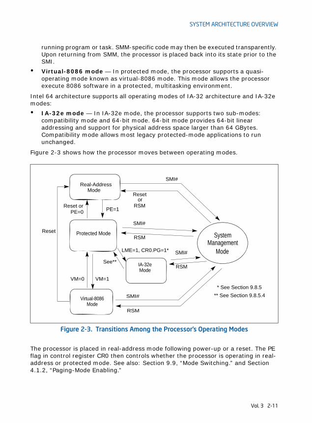
2.2 MODES OF OPERATIONThe IA-32 supports three operating modes and one quasi-operating mode:
• Protected mode — This is the native operating mode of the processor. It provides a rich set of architectural features, flexibility, high performance and backward compatibility to existing software base.
• Real-address mode — This operating mode provides the programming environment of the Intel 8086 processor, with a few extensions (such as the ability to switch to protected or system management mode).
• System management mode (SMM) — SMM is a standard architectural feature in all IA-32 processors, beginning with the Intel386 SL processor. This mode provides an operating system or executive with a transparent mechanism for implementing power management and OEM differentiation features. SMM is entered through activation of an external system interrupt pin (SMI#), which generates a system management interrupt (SMI). In SMM, the processor switches to a separate address space while saving the context of the currently
2-10 Vol. 3
SYSTEM ARCHITECTURE OVERVIEW
running program or task. SMM-specific code may then be executed transparently. Upon returning from SMM, the processor is placed back into its state prior to the SMI.
• Virtual-8086 mode — In protected mode, the processor supports a quasi-operating mode known as virtual-8086 mode. This mode allows the processor execute 8086 software in a protected, multitasking environment.
Intel 64 architecture supports all operating modes of IA-32 architecture and IA-32e modes:
• IA-32e mode — In IA-32e mode, the processor supports two sub-modes: compatibility mode and 64-bit mode. 64-bit mode provides 64-bit linear addressing and support for physical address space larger than 64 GBytes. Compatibility mode allows most legacy protected-mode applications to run unchanged.
Figure 2-3 shows how the processor moves between operating modes.
The processor is placed in real-address mode following power-up or a reset. The PE flag in control register CR0 then controls whether the processor is operating in real-address or protected mode. See also: Section 9.9, “Mode Switching.” and Section 4.1.2, “Paging-Mode Enabling.”
Figure 2-3. Transitions Among the Processor’s Operating Modes
Real-Address
Protected Mode
Virtual-8086Mode
SystemManagement
Mode
PE=1Reset or
VM=1VM=0
PE=0
Resetor
RSM
SMI#
RSM
SMI#
RSM
SMI#Reset
Mode
IA-32eMode
RSM
SMI#LME=1, CR0.PG=1*
See**
* See Section 9.8.5** See Section 9.8.5.4
Vol. 3 2-11

SYSTEM ARCHITECTURE OVERVIEW
The VM flag in the EFLAGS register determines whether the processor is operating in protected mode or virtual-8086 mode. Transitions between protected mode and virtual-8086 mode are generally carried out as part of a task switch or a return from an interrupt or exception handler. See also: Section 17.2.5, “Entering Virtual-8086 Mode.”
The LMA bit (IA32_EFER.LMA.LMA[bit 10]) determines whether the processor is operating in IA-32e mode. When running in IA-32e mode, 64-bit or compatibility sub-mode operation is determined by CS.L bit of the code segment. The processor enters into IA-32e mode from protected mode by enabling paging and setting the LME bit (IA32_EFER.LME[bit 8]). See also: Chapter 9, “Processor Management and Initialization.”
The processor switches to SMM whenever it receives an SMI while the processor is in real-address, protected, virtual-8086, or IA-32e modes. Upon execution of the RSM instruction, the processor always returns to the mode it was in when the SMI occurred.
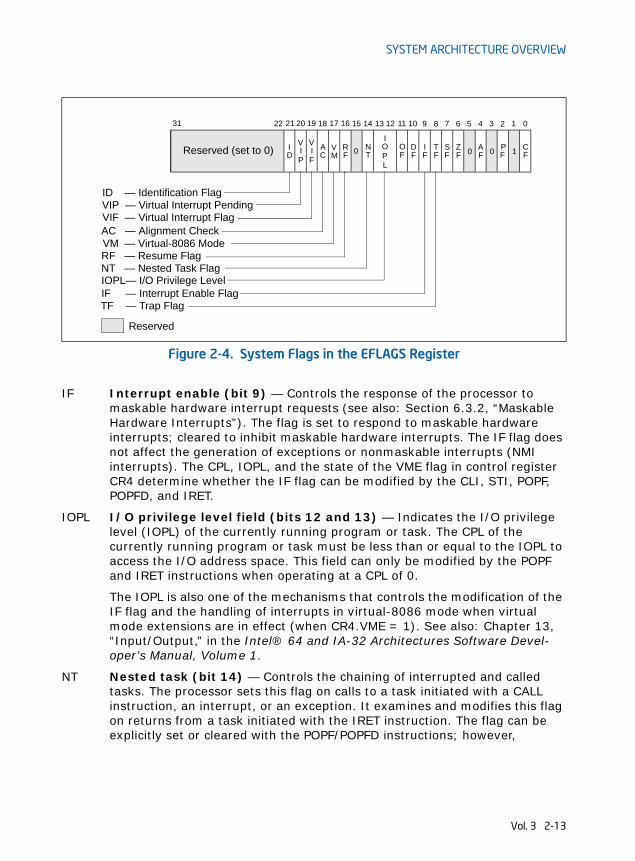
2.3 SYSTEM FLAGS AND FIELDS IN THE EFLAGS REGISTER
The system flags and IOPL field of the EFLAGS register control I/O, maskable hard-ware interrupts, debugging, task switching, and the virtual-8086 mode (see Figure 2-4). Only privileged code (typically operating system or executive code) should be allowed to modify these bits.
The system flags and IOPL are:
TF Trap (bit 8) — Set to enable single-step mode for debugging; clear to disable single-step mode. In single-step mode, the processor generates a debug exception after each instruction. This allows the execution state of a program to be inspected after each instruction. If an application program sets the TF flag using a POPF, POPFD, or IRET instruction, a debug exception is generated after the instruction that follows the POPF, POPFD, or IRET.
2-12 Vol. 3
SYSTEM ARCHITECTURE OVERVIEW
IF Interrupt enable (bit 9) — Controls the response of the processor to maskable hardware interrupt requests (see also: Section 6.3.2, “Maskable Hardware Interrupts”). The flag is set to respond to maskable hardware interrupts; cleared to inhibit maskable hardware interrupts. The IF flag does not affect the generation of exceptions or nonmaskable interrupts (NMI interrupts). The CPL, IOPL, and the state of the VME flag in control register CR4 determine whether the IF flag can be modified by the CLI, STI, POPF, POPFD, and IRET.
IOPL I/O privilege level field (bits 12 and 13) — Indicates the I/O privilege level (IOPL) of the currently running program or task. The CPL of the currently running program or task must be less than or equal to the IOPL to access the I/O address space. This field can only be modified by the POPF and IRET instructions when operating at a CPL of 0.
The IOPL is also one of the mechanisms that controls the modification of the IF flag and the handling of interrupts in virtual-8086 mode when virtual mode extensions are in effect (when CR4.VME = 1). See also: Chapter 13, “Input/Output,” in the Intel® 64 and IA-32 Architectures Software Devel-oper’s Manual, Volume 1.
NT Nested task (bit 14) — Controls the chaining of interrupted and called tasks. The processor sets this flag on calls to a task initiated with a CALL instruction, an interrupt, or an exception. It examines and modifies this flag on returns from a task initiated with the IRET instruction. The flag can be explicitly set or cleared with the POPF/POPFD instructions; however,
Figure 2-4. System Flags in the EFLAGS Register
31 22 21 20 19 18 17 16
RF
ID
AC
VM
VM — Virtual-8086 ModeRF — Resume FlagNT — Nested Task FlagIOPL— I/O Privilege LevelIF — Interrupt Enable Flag
AC — Alignment Check
ID — Identification FlagVIP — Virtual Interrupt Pending
15 1314 12 11 10 9 8 7 6 5 4 3 2 1 0
0 CF
AF
PF 1D
FIF
TF
SF
ZF
NT 00
VIP
VIF
OF
IOPL
VIF — Virtual Interrupt Flag
TF — Trap Flag
Reserved
Reserved (set to 0)
Vol. 3 2-13

SYSTEM ARCHITECTURE OVERVIEW
changing to the state of this flag can generate unexpected exceptions in application programs.
See also: Section 7.4, “Task Linking.”
RF Resume (bit 16) — Controls the processor’s response to instruction-break-point conditions. When set, this flag temporarily disables debug exceptions (#DB) from being generated for instruction breakpoints (although other exception conditions can cause an exception to be generated). When clear, instruction breakpoints will generate debug exceptions.
The primary function of the RF flag is to allow the restarting of an instruction following a debug exception that was caused by an instruction breakpoint condition. Here, debug software must set this flag in the EFLAGS image on the stack just prior to returning to the interrupted program with IRETD (to prevent the instruction breakpoint from causing another debug exception). The processor then automatically clears this flag after the instruction returned to has been successfully executed, enabling instruction breakpoint faults again.
See also: Section 16.3.1.1, “Instruction-Breakpoint Exception Condition.”
VM Virtual-8086 mode (bit 17) — Set to enable virtual-8086 mode; clear to return to protected mode.
See also: Section 17.2.1, “Enabling Virtual-8086 Mode.”
AC Alignment check (bit 18) — Set this flag and the AM flag in control register CR0 to enable alignment checking of memory references; clear the AC flag and/or the AM flag to disable alignment checking. An alignment-check exception is generated when reference is made to an unaligned operand, such as a word at an odd byte address or a doubleword at an address which is not an integral multiple of four. Alignment-check exceptions are generated only in user mode (privilege level 3). Memory references that default to priv-ilege level 0, such as segment descriptor loads, do not generate this excep-tion even when caused by instructions executed in user-mode.
The alignment-check exception can be used to check alignment of data. This is useful when exchanging data with processors which require all data to be aligned. The alignment-check exception can also be used by interpreters to flag some pointers as special by misaligning the pointer. This eliminates overhead of checking each pointer and only handles the special pointer when used.
VIF Virtual Interrupt (bit 19) — Contains a virtual image of the IF flag. This flag is used in conjunction with the VIP flag. The processor only recognizes the VIF flag when either the VME flag or the PVI flag in control register CR4 is set and the IOPL is less than 3. (The VME flag enables the virtual-8086 mode extensions; the PVI flag enables the protected-mode virtual interrupts.)
See also: Section 17.3.3.5, “Method 6: Software Interrupt Handling,” and Section 17.4, “Protected-Mode Virtual Interrupts.”
2-14 Vol. 3

SYSTEM ARCHITECTURE OVERVIEW
VIP Virtual interrupt pending (bit 20) — Set by software to indicate that an interrupt is pending; cleared to indicate that no interrupt is pending. This flag is used in conjunction with the VIF flag. The processor reads this flag but never modifies it. The processor only recognizes the VIP flag when either the VME flag or the PVI flag in control register CR4 is set and the IOPL is less than 3. The VME flag enables the virtual-8086 mode extensions; the PVI flag enables the protected-mode virtual interrupts.
See Section 17.3.3.5, “Method 6: Software Interrupt Handling,” and Section 17.4, “Protected-Mode Virtual Interrupts.”
ID Identification (bit 21). — The ability of a program or procedure to set or clear this flag indicates support for the CPUID instruction.
2.3.1 System Flags and Fields in IA-32e ModeIn 64-bit mode, the RFLAGS register expands to 64 bits with the upper 32 bits reserved. System flags in RFLAGS (64-bit mode) or EFLAGS (compatibility mode) are shown in Figure 2-4.
In IA-32e mode, the processor does not allow the VM bit to be set because virtual-8086 mode is not supported (attempts to set the bit are ignored). Also, the processor will not set the NT bit. The processor does, however, allow software to set the NT bit (note that an IRET causes a general protection fault in IA-32e mode if the NT bit is set).
In IA-32e mode, the SYSCALL/SYSRET instructions have a programmable method of specifying which bits are cleared in RFLAGS/EFLAGS. These instructions save/restore EFLAGS/RFLAGS.
2.4 MEMORY-MANAGEMENT REGISTERSThe processor provides four memory-management registers (GDTR, LDTR, IDTR, and TR) that specify the locations of the data structures which control segmented memory management (see Figure 2-5). Special instructions are provided for loading and storing these registers.
Vol. 3 2-15

SYSTEM ARCHITECTURE OVERVIEW
2.4.1 Global Descriptor Table Register (GDTR)The GDTR register holds the base address (32 bits in protected mode; 64 bits in IA-32e mode) and the 16-bit table limit for the GDT. The base address specifies the linear address of byte 0 of the GDT; the table limit specifies the number of bytes in the table.
The LGDT and SGDT instructions load and store the GDTR register, respectively. On power up or reset of the processor, the base address is set to the default value of 0 and the limit is set to 0FFFFH. A new base address must be loaded into the GDTR as part of the processor initialization process for protected-mode operation.
See also: Section 3.5.1, “Segment Descriptor Tables.”
2.4.2 Local Descriptor Table Register (LDTR)The LDTR register holds the 16-bit segment selector, base address (32 bits in protected mode; 64 bits in IA-32e mode), segment limit, and descriptor attributes for the LDT. The base address specifies the linear address of byte 0 of the LDT segment; the segment limit specifies the number of bytes in the segment. See also: Section 3.5.1, “Segment Descriptor Tables.”
The LLDT and SLDT instructions load and store the segment selector part of the LDTR register, respectively. The segment that contains the LDT must have a segment descriptor in the GDT. When the LLDT instruction loads a segment selector in the LDTR: the base address, limit, and descriptor attributes from the LDT descriptor are automatically loaded in the LDTR.
When a task switch occurs, the LDTR is automatically loaded with the segment selector and descriptor for the LDT for the new task. The contents of the LDTR are not automatically saved prior to writing the new LDT information into the register.
On power up or reset of the processor, the segment selector and base address are set to the default value of 0 and the limit is set to 0FFFFH.
Figure 2-5. Memory Management Registers
047(79)
GDTRIDTR
System Table Registers
32(64)-bit Linear Base Address 16-Bit Table Limit
1516
32(64)-bit Linear Base Address
0Task
LDTR
System Segment
Seg. Sel.
15
Seg. Sel.
Segment Descriptor Registers (Automatically Loaded)
32(64)-bit Linear Base Address Segment Limit
AttributesRegisters
32(64)-bit Linear Base Address Segment LimitRegister
16-Bit Table Limit
2-16 Vol. 3

SYSTEM ARCHITECTURE OVERVIEW
2.4.3 IDTR Interrupt Descriptor Table RegisterThe IDTR register holds the base address (32 bits in protected mode; 64 bits in IA-32e mode) and 16-bit table limit for the IDT. The base address specifies the linear address of byte 0 of the IDT; the table limit specifies the number of bytes in the table. The LIDT and SIDT instructions load and store the IDTR register, respectively. On power up or reset of the processor, the base address is set to the default value of 0 and the limit is set to 0FFFFH. The base address and limit in the register can then be changed as part of the processor initialization process.
See also: Section 6.10, “Interrupt Descriptor Table (IDT).”
2.4.4 Task Register (TR)The task register holds the 16-bit segment selector, base address (32 bits in protected mode; 64 bits in IA-32e mode), segment limit, and descriptor attributes for the TSS of the current task. The selector references the TSS descriptor in the GDT. The base address specifies the linear address of byte 0 of the TSS; the segment limit specifies the number of bytes in the TSS. See also: Section 7.2.4, “Task Register.”
The LTR and STR instructions load and store the segment selector part of the task register, respectively. When the LTR instruction loads a segment selector in the task register, the base address, limit, and descriptor attributes from the TSS descriptor are automatically loaded into the task register. On power up or reset of the processor, the base address is set to the default value of 0 and the limit is set to 0FFFFH.
When a task switch occurs, the task register is automatically loaded with the segment selector and descriptor for the TSS for the new task. The contents of the task register are not automatically saved prior to writing the new TSS information into the register.
2.5 CONTROL REGISTERSControl registers (CR0, CR1, CR2, CR3, and CR4; see Figure 2-6) determine oper-ating mode of the processor and the characteristics of the currently executing task. These registers are 32 bits in all 32-bit modes and compatibility mode.
In 64-bit mode, control registers are expanded to 64 bits. The MOV CRn instructions are used to manipulate the register bits. Operand-size prefixes for these instructions are ignored. The following is also true:
• Bits 63:32 of CR0 and CR4 are reserved and must be written with zeros. Writing a nonzero value to any of the upper 32 bits results in a general-protection exception, #GP(0).
• All 64 bits of CR2 are writable by software.
• Bits 51:40 of CR3 are reserved and must be 0.
Vol. 3 2-17

SYSTEM ARCHITECTURE OVERVIEW
• The MOV CRn instructions do not check that addresses written to CR2 and CR3 are within the linear-address or physical-address limitations of the implemen-tation.
• Register CR8 is available in 64-bit mode only.
The control registers are summarized below, and each architecturally defined control field in these control registers are described individually. In Figure 2-6, the width of the register in 64-bit mode is indicated in parenthesis (except for CR0).
• CR0 — Contains system control flags that control operating mode and states of the processor.
• CR1 — Reserved.
• CR2 — Contains the page-fault linear address (the linear address that caused a page fault).
• CR3 — Contains the physical address of the base of the paging-structure hierarchy and two flags (PCD and PWT). Only the most-significant bits (less the lower 12 bits) of the base address are specified; the lower 12 bits of the address are assumed to be 0. The first paging structure must thus be aligned to a page (4-KByte) boundary. The PCD and PWT flags control caching of that paging structure in the processor’s internal data caches (they do not control TLB caching of page-directory information).
When using the physical address extension, the CR3 register contains the base address of the page-directory-pointer table In IA-32e mode, the CR3 register contains the base address of the PML4 table.
See also: Chapter 4, “Paging.”
• CR4 — Contains a group of flags that enable several architectural extensions, and indicate operating system or executive support for specific processor capabil-ities. The control registers can be read and loaded (or modified) using the move-to-or-from-control-registers forms of the MOV instruction. In protected mode, the MOV instructions allow the control registers to be read or loaded (at privilege level 0 only). This restriction means that application programs or operating-system procedures (running at privilege levels 1, 2, or 3) are prevented from reading or loading the control registers.
• CR8 — Provides read and write access to the Task Priority Register (TPR). It specifies the priority threshold value that operating systems use to control the priority class of external interrupts allowed to interrupt the processor. This register is available only in 64-bit mode. However, interrupt filtering continues to apply in compatibility mode.
2-18 Vol. 3

SYSTEM ARCHITECTURE OVERVIEW
When loading a control register, reserved bits should always be set to the values previously read. The flags in control registers are:
PG Paging (bit 31 of CR0) — Enables paging when set; disables paging when clear. When paging is disabled, all linear addresses are treated as physical addresses. The PG flag has no effect if the PE flag (bit 0 of register CR0) is not also set; setting the PG flag when the PE flag is clear causes a general-protection exception (#GP). See also: Chapter 4, “Paging.”
On Intel 64 processors, enabling and disabling IA-32e mode operation also requires modifying CR0.PG.
CD Cache Disable (bit 30 of CR0) — When the CD and NW flags are clear, caching of memory locations for the whole of physical memory in the processor’s internal (and external) caches is enabled. When the CD flag is set, caching is restricted as described in Table 11-5. To prevent the processor from accessing and updating its caches, the CD flag must be set and the caches must be invalidated so that no cache hits can occur.
Figure 2-6. Control Registers
CR1
WP
AM
Page-Directory Base
VME
PSE
TSD
DE
PVI
PGE
MCE
PAE
PCE
NW
PG
CD
PWT
PCD
Page-Fault Linear Address
PE
EM
MP
TS
NE
ET
CR2
CR0
CR4
Reserved
CR3
Reserved (set to 0)
31 2930 28 19 18 17 16 15 6 5 4 3 2 1 0
31(63) 0
31(63) 0
31(63) 12 11 5 4 3 2
31(63) 9 8 7 6 5 4 3 2 1 0
(PDBR)
13 12 11 10
OSFXSROSXMMEXCPT
VMXE
00
EXMS
1418
OSXSAVEPCIDE
17
Vol. 3 2-19

SYSTEM ARCHITECTURE OVERVIEW
Software can access XCR0 only if CR4.OSXSAVE[bit 18] = 1. (This bit is also readable as CPUID.01H:ECX.OSXSAVE[bit 27].) The layout of XCR0 is architected to allow software to use CPUID leaf function 0DH to enumerate the set of bits that the processor supports in XCR0 (see CPUID instruction in Intel® 64 and IA-32 Architec-tures Software Developer’s Manual, Volume 2A). Each processor state (X87 FPU state, SSE state, or a future processor extended state) is represented by a bit in XCR0. The OS can enable future processor extended states in a forward manner by specifying the appropriate bit mask value using the XSETBV instruction according to the results of the CPUID leaf 0DH.
With the exception of bit 63, each bit in the XFEATURE_ENABLED_MASK register (XCR0) corresponds to a subset of the processor states. XCR0 thus provides space for up to 63 sets of processor state extensions. Bit 63 of XCR0 is reserved for future expansion and will not represent a processor extended state.
Currently, the XFEATURE_ENABLED_MASK register (XCR0) has two processor states defined, with up to 61 bits reserved for future processor extended states:
• XCR0.X87 (bit 0): If 1, indicates x87 FPU state (including MMX register states) is supported in the processor. Bit 0 must be 1. An attempt to write 0 causes a #GP exception.
• XCR0.SSE (bit 1): If 1, indicates MXCSR and XMM registers (XMM0-XMM15 in 64-bit mode, otherwise XMM0-XMM7) are supported by XSAVE/XRESTOR in the processor.
Any attempt to set a reserved bit (as determined by the contents of EAX and EDX after executing CPUID with EAX=0DH, ECX= 0H) in the XFEATURE_ENABLED_MASK register for a given processor will result in a #GP exception. An attempt to write 0 to XFEATURE_ENABLED_MASK.x87 (bit 0) will result in a #GP exception.
If a bit in the XFEATURE_ENABLED_MASK register is 1, XSAVE instruction can selec-tively (in conjunction with a save mask) save a partial or full set of processor states to memory (See XSAVE instruction in Intel® 64 and IA-32 Architectures Software Developer’s Manual, Volume 2B).
After reset all bits (except bit 0) in the XFEATURE_ENABLED_MASK register (XCR0) are cleared to zero. XCR0[0] is set to 1.
2.7 SYSTEM INSTRUCTION SUMMARYSystem instructions handle system-level functions such as loading system registers, managing the cache, managing interrupts, or setting up the debug registers. Many of these instructions can be executed only by operating-system or executive proce-dures (that is, procedures running at privilege level 0). Others can be executed at any privilege level and are thus available to application programs.
Table 2-2 lists the system instructions and indicates whether they are available and useful for application programs. These instructions are described in the Intel® 64 and IA-32 Architectures Software Developer’s Manual, Volumes 2A & 2B.
Vol. 3 2-27

SYSTEM ARCHITECTURE OVERVIEW
Table 2-2. Summary of System Instructions
Instruction DescriptionUseful toApplication?
Protected fromApplication?
LLDT Load LDT Register No Yes
SLDT Store LDT Register No No
LGDT Load GDT Register No Yes
SGDT Store GDT Register No No
LTR Load Task Register No Yes
STR Store Task Register No No
LIDT Load IDT Register No Yes
SIDT Store IDT Register No No
MOV CRn Load and store control registers No Yes
SMSW Store MSW Yes No
LMSW Load MSW No Yes
CLTS Clear TS flag in CR0 No Yes
ARPL Adjust RPL Yes1, 5 No
LAR Load Access Rights Yes No
LSL Load Segment Limit Yes No
VERR Verify for Reading Yes No
VERW Verify for Writing Yes No
MOV DRn Load and store debug registers No Yes
INVD Invalidate cache, no writeback No Yes
WBINVD Invalidate cache, with writeback No Yes
INVLPG Invalidate TLB entry No Yes
HLT Halt Processor No Yes
LOCK (Prefix) Bus Lock Yes No
RSM Return from system management mode
No Yes
RDMSR3 Read Model-Specific Registers No Yes
WRMSR3 Write Model-Specific Registers No Yes
RDPMC4 Read Performance-Monitoring Counter
Yes Yes2
RDTSC3 Read Time-Stamp Counter Yes Yes2
2-28 Vol. 3
SYSTEM ARCHITECTURE OVERVIEW
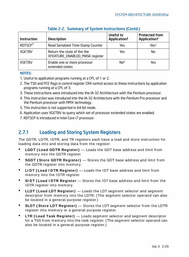
2.7.1 Loading and Storing System RegistersThe GDTR, LDTR, IDTR, and TR registers each have a load and store instruction for loading data into and storing data from the register:
• LGDT (Load GDTR Register) — Loads the GDT base address and limit from memory into the GDTR register.
• SGDT (Store GDTR Register) — Stores the GDT base address and limit from the GDTR register into memory.
• LIDT (Load IDTR Register) — Loads the IDT base address and limit from memory into the IDTR register.
• SIDT (Load IDTR Register — Stores the IDT base address and limit from the IDTR register into memory.
• LLDT (Load LDT Register) — Loads the LDT segment selector and segment descriptor from memory into the LDTR. (The segment selector operand can also be located in a general-purpose register.)
• SLDT (Store LDT Register) — Stores the LDT segment selector from the LDTR register into memory or a general-purpose register.
• LTR (Load Task Register) — Loads segment selector and segment descriptor for a TSS from memory into the task register. (The segment selector operand can also be located in a general-purpose register.)
RDTSCP7 Read Serialized Time-Stamp Counter Yes Yes2
XGETBV Return the state of the the XFEATURE_ENABLED_MASK register
Yes No
XSETBV Enable one or more processor extended states
No6 Yes
NOTES:1. Useful to application programs running at a CPL of 1 or 2.2. The TSD and PCE flags in control register CR4 control access to these instructions by application
programs running at a CPL of 3.3. These instructions were introduced into the IA-32 Architecture with the Pentium processor.4. This instruction was introduced into the IA-32 Architecture with the Pentium Pro processor and
the Pentium processor with MMX technology.5. This instruction is not supported in 64-bit mode.6. Application uses XGETBV to query which set of processor extended states are enabled.7. RDTSCP is introduced in Intel Core i7 processor.
Table 2-2. Summary of System Instructions (Contd.)
Instruction DescriptionUseful toApplication?
Protected fromApplication?
Vol. 3 2-29

SYSTEM ARCHITECTURE OVERVIEW
• STR (Store Task Register) — Stores the segment selector for the current task TSS from the task register into memory or a general-purpose register.
The LMSW (load machine status word) and SMSW (store machine status word) instructions operate on bits 0 through 15 of control register CR0. These instructions are provided for compatibility with the 16-bit Intel 286 processor. Programs written to run on 32-bit IA-32 processors should not use these instructions. Instead, they should access the control register CR0 using the MOV instruction.
The CLTS (clear TS flag in CR0) instruction is provided for use in handling a device-not-available exception (#NM) that occurs when the processor attempts to execute a floating-point instruction when the TS flag is set. This instruction allows the TS flag to be cleared after the x87 FPU context has been saved, preventing further #NM exceptions. See Section 2.5, “Control Registers,” for more information on the TS flag.
The control registers (CR0, CR1, CR2, CR3, CR4, and CR8) are loaded using the MOV instruction. The instruction loads a control register from a general-purpose register or stores the content of a control register in a general-purpose register.
2.7.2 Verifying of Access PrivilegesThe processor provides several instructions for examining segment selectors and segment descriptors to determine if access to their associated segments is allowed. These instructions duplicate some of the automatic access rights and type checking done by the processor, thus allowing operating-system or executive software to prevent exceptions from being generated.
The ARPL (adjust RPL) instruction adjusts the RPL (requestor privilege level) of a segment selector to match that of the program or procedure that supplied the segment selector. See Section 5.10.4, “Checking Caller Access Privileges (ARPL Instruction),” for a detailed explanation of the function and use of this instruction. Note that ARPL is not supported in 64-bit mode.
The LAR (load access rights) instruction verifies the accessibility of a speci-fied segment and loads access rights information from the segment’s segment descriptor into a general-purpose register. Software can then examine the access rights to determine if the segment type is compatible with its intended use. See Section 5.10.1, “Checking Access Rights (LAR Instruction),” for a detailed explanation of the function and use of this instruction.
The LSL (load segment limit) instruction verifies the accessibility of a speci-fied segment and loads the segment limit from the segment’s segment descriptor into a general-purpose register. Software can then compare the segment limit with an offset into the segment to determine whether the offset lies within the segment. See Section 5.10.3, “Checking That the Pointer Offset Is Within Limits (LSL Instruction),” for a detailed explanation of the function and use of this instruction.
2-30 Vol. 3

SYSTEM ARCHITECTURE OVERVIEW
The VERR (verify for reading) and VERW (verify for writing) instructions verify if a selected segment is readable or writable, respectively, at a given CPL. See Section 5.10.2, “Checking Read/Write Rights (VERR and VERW Instructions),” for a detailed explanation of the function and use of this instruction.
2.7.3 Loading and Storing Debug RegistersInternal debugging facilities in the processor are controlled by a set of 8 debug regis-ters (DR0-DR7). The MOV instruction allows setup data to be loaded to and stored from these registers.
On processors that support Intel 64 architecture, debug registers DR0-DR7 are 64 bits. In 32-bit modes and compatibility mode, writes to a debug register fill the upper 32 bits with zeros. Reads return the lower 32 bits. In 64-bit mode, the upper 32 bits of DR6-DR7 are reserved and must be written with zeros. Writing one to any of the upper 32 bits causes an exception, #GP(0).
In 64-bit mode, MOV DRn instructions read or write all 64 bits of a debug register (operand-size prefixes are ignored). All 64 bits of DR0-DR3 are writable by software. However, MOV DRn instructions do not check that addresses written to DR0-DR3 are in the limits of the implementation. Address matching is supported only on valid addresses generated by the processor implementation.
2.7.4 Invalidating Caches and TLBsThe processor provides several instructions for use in explicitly invalidating its caches and TLB entries. The INVD (invalidate cache with no writeback) instruction invali-dates all data and instruction entries in the internal caches and sends a signal to the external caches indicating that they should be also be invalidated.
The WBINVD (invalidate cache with writeback) instruction performs the same func-tion as the INVD instruction, except that it writes back modified lines in its internal caches to memory before it invalidates the caches. After invalidating the internal caches, WBINVD signals external caches to write back modified data and invalidate their contents.
The INVLPG (invalidate TLB entry) instruction invalidates (flushes) the TLB entry for a specified page.
2.7.5 Controlling the Processor
The HLT (halt processor) instruction stops the processor until an enabled interrupt (such as NMI or SMI, which are normally enabled), a debug exception, the BINIT# signal, the INIT# signal, or the RESET# signal is received. The processor generates a special bus cycle to indicate that the halt mode has been entered.
Vol. 3 2-31

SYSTEM ARCHITECTURE OVERVIEW
Hardware may respond to this signal in a number of ways. An indicator light on the front panel may be turned on. An NMI interrupt for recording diagnostic information may be generated. Reset initialization may be invoked (note that the BINIT# pin was introduced with the Pentium Pro processor). If any non-wake events are pending during shutdown, they will be handled after the wake event from shutdown is processed (for example, A20M# interrupts).
The LOCK prefix invokes a locked (atomic) read-modify-write operation when modi-fying a memory operand. This mechanism is used to allow reliable communications between processors in multiprocessor systems, as described below:
• In the Pentium processor and earlier IA-32 processors, the LOCK prefix causes the processor to assert the LOCK# signal during the instruction. This always causes an explicit bus lock to occur.
• In the Pentium 4, Intel Xeon, and P6 family processors, the locking operation is handled with either a cache lock or bus lock. If a memory access is cacheable and affects only a single cache line, a cache lock is invoked and the system bus and the actual memory location in system memory are not locked during the operation. Here, other Pentium 4, Intel Xeon, or P6 family processors on the bus write-back any modified data and invalidate their caches as necessary to maintain system memory coherency. If the memory access is not cacheable and/or it crosses a cache line boundary, the processor’s LOCK# signal is asserted and the processor does not respond to requests for bus control during the locked operation.
The RSM (return from SMM) instruction restores the processor (from a context dump) to the state it was in prior to an system management mode (SMM) interrupt.
2.7.6 Reading Performance-Monitoring and Time-Stamp CountersThe RDPMC (read performance-monitoring counter) and RDTSC (read time-stamp counter) instructions allow application programs to read the processor’s perfor-mance-monitoring and time-stamp counters, respectively. Processors based on Intel NetBurst® microarchitecture have eighteen 40-bit performance-monitoring counters; P6 family processors have two 40-bit counters. Intel® Atom™ processors and most of the processors based on the Intel Core microarchitecture support two types of performance monitoring counters: two programmable performance counters similar to those available in the P6 family, and three fixed-function perfor-mance monitoring counters.
The programmable performance counters can support counting either the occurrence or duration of events. Events that can be monitored on programmable counters generally are model specific (except for architectural performance events enumer-ated by CPUID leaf 0AH); they may include the number of instructions decoded, interrupts received, or the number of cache loads. Individual counters can be set up to monitor different events. Use the system instruction WRMSR to set up values in IA32_PERFEVTSEL0/1 (for Intel Atom, Intel Core 2, Intel Core Duo, and Intel Pentium M processors), in one of the 45 ESCRs and one of the 18 CCCR MSRs (for
2-32 Vol. 3

CHAPTER 3PROTECTED-MODE MEMORY MANAGEMENT
This chapter describes the Intel 64 and IA-32 architecture’s protected-mode memory management facilities, including the physical memory requirements, segmentation mechanism, and paging mechanism.
See also: Chapter 5, “Protection” (for a description of the processor’s protection mechanism) and Chapter 17, “8086 Emulation” (for a description of memory addressing protection in real-address and virtual-8086 modes).
3.1 MEMORY MANAGEMENT OVERVIEWThe memory management facilities of the IA-32 architecture are divided into two parts: segmentation and paging. Segmentation provides a mechanism of isolating individual code, data, and stack modules so that multiple programs (or tasks) can run on the same processor without interfering with one another. Paging provides a mechanism for implementing a conventional demand-paged, virtual-memory system where sections of a program’s execution environment are mapped into physical memory as needed. Paging can also be used to provide isolation between multiple tasks. When operating in protected mode, some form of segmentation must be used. There is no mode bit to disable segmentation. The use of paging, however, is optional.
These two mechanisms (segmentation and paging) can be configured to support simple single-program (or single-task) systems, multitasking systems, or multiple-processor systems that used shared memory.
As shown in Figure 3-1, segmentation provides a mechanism for dividing the processor’s addressable memory space (called the linear address space) into smaller protected address spaces called segments. Segments can be used to hold the code, data, and stack for a program or to hold system data structures (such as a TSS or LDT). If more than one program (or task) is running on a processor, each program can be assigned its own set of segments. The processor then enforces the boundaries between these segments and insures that one program does not interfere with the execution of another program by writing into the other program’s segments. The segmentation mechanism also allows typing of segments so that the operations that may be performed on a particular type of segment can be restricted.
All the segments in a system are contained in the processor’s linear address space. To locate a byte in a particular segment, a logical address (also called a far pointer) must be provided. A logical address consists of a segment selector and an offset. The segment selector is a unique identifier for a segment. Among other things it provides an offset into a descriptor table (such as the global descriptor table, GDT) to a data structure called a segment descriptor. Each segment has a segment descriptor, which specifies the size of the segment, the access rights and privilege level for the
Vol. 3 3-1

PROTECTED-MODE MEMORY MANAGEMENT
segment, the segment type, and the location of the first byte of the segment in the linear address space (called the base address of the segment). The offset part of the logical address is added to the base address for the segment to locate a byte within the segment. The base address plus the offset thus forms a linear address in the processor’s linear address space.
If paging is not used, the linear address space of the processor is mapped directly into the physical address space of processor. The physical address space is defined as the range of addresses that the processor can generate on its address bus.
Because multitasking computing systems commonly define a linear address space much larger than it is economically feasible to contain all at once in physical memory, some method of “virtualizing” the linear address space is needed. This virtualization of the linear address space is handled through the processor’s paging mechanism.
Paging supports a “virtual memory” environment where a large linear address space is simulated with a small amount of physical memory (RAM and ROM) and some disk
Figure 3-1. Segmentation and Paging
Global DescriptorTable (GDT)
Linear AddressSpace
SegmentSegmentDescriptor
Offset
Logical Address
SegmentBase Address
Page
Phy. Addr.Lin. Addr.
SegmentSelector
Dir Table OffsetLinear Address
Page Table
Page Directory
Entry
Physical
Space
Entry
(or Far Pointer)
PagingSegmentation
Address
Page
3-2 Vol. 3

PROTECTED-MODE MEMORY MANAGEMENT
storage. When using paging, each segment is divided into pages (typically 4 KBytes each in size), which are stored either in physical memory or on the disk. The oper-ating system or executive maintains a page directory and a set of page tables to keep track of the pages. When a program (or task) attempts to access an address location in the linear address space, the processor uses the page directory and page tables to translate the linear address into a physical address and then performs the requested operation (read or write) on the memory location.
If the page being accessed is not currently in physical memory, the processor inter-rupts execution of the program (by generating a page-fault exception). The oper-ating system or executive then reads the page into physical memory from the disk and continues executing the program.
When paging is implemented properly in the operating-system or executive, the swapping of pages between physical memory and the disk is transparent to the correct execution of a program. Even programs written for 16-bit IA-32 processors can be paged (transparently) when they are run in virtual-8086 mode.
3.2 USING SEGMENTSThe segmentation mechanism supported by the IA-32 architecture can be used to implement a wide variety of system designs. These designs range from flat models that make only minimal use of segmentation to protect programs to multi-segmented models that employ segmentation to create a robust operating environ-ment in which multiple programs and tasks can be executed reliably.
The following sections give several examples of how segmentation can be employed in a system to improve memory management performance and reliability.
3.2.1 Basic Flat ModelThe simplest memory model for a system is the basic “flat model,” in which the oper-ating system and application programs have access to a continuous, unsegmented address space. To the greatest extent possible, this basic flat model hides the segmentation mechanism of the architecture from both the system designer and the application programmer.
To implement a basic flat memory model with the IA-32 architecture, at least two segment descriptors must be created, one for referencing a code segment and one for referencing a data segment (see Figure 3-2). Both of these segments, however, are mapped to the entire linear address space: that is, both segment descriptors have the same base address value of 0 and the same segment limit of 4 GBytes. By setting the segment limit to 4 GBytes, the segmentation mechanism is kept from generating exceptions for out of limit memory references, even if no physical memory resides at a particular address. ROM (EPROM) is generally located at the top of the physical address space, because the processor begins execution at
Vol. 3 3-3

PROTECTED-MODE MEMORY MANAGEMENT
FFFF_FFF0H. RAM (DRAM) is placed at the bottom of the address space because the initial base address for the DS data segment after reset initialization is 0.
3.2.2 Protected Flat ModelThe protected flat model is similar to the basic flat model, except the segment limits are set to include only the range of addresses for which physical memory actually exists (see Figure 3-3). A general-protection exception (#GP) is then generated on any attempt to access nonexistent memory. This model provides a minimum level of hardware protection against some kinds of program bugs.
Figure 3-2. Flat Model
Figure 3-3. Protected Flat Model
Linear Address Space(or Physical Memory)
Data and
FFFFFFFFHSegment
LimitAccessBase Address
RegistersCS
SS
DS
ES
FS
GS
Code
0
Code- and Data-SegmentDescriptors
Stack
Not Present
Linear Address Space(or Physical Memory)
Data and
FFFFFFFFHSegment
LimitAccessBase Address
Registers
CS
ES
SS
DS
FS
GS
Code
0
SegmentDescriptors
LimitAccessBase Address
Memory I/O
Stack
Not Present
3-4 Vol. 3
PROTECTED-MODE MEMORY MANAGEMENT
More complexity can be added to this protected flat model to provide more protec-tion. For example, for the paging mechanism to provide isolation between user and supervisor code and data, four segments need to be defined: code and data segments at privilege level 3 for the user, and code and data segments at privilege level 0 for the supervisor. Usually these segments all overlay each other and start at address 0 in the linear address space. This flat segmentation model along with a simple paging structure can protect the operating system from applications, and by adding a separate paging structure for each task or process, it can also protect appli-cations from each other. Similar designs are used by several popular multitasking operating systems.
3.2.3 Multi-Segment ModelA multi-segment model (such as the one shown in Figure 3-4) uses the full capabili-ties of the segmentation mechanism to provided hardware enforced protection of code, data structures, and programs and tasks. Here, each program (or task) is given its own table of segment descriptors and its own segments. The segments can be completely private to their assigned programs or shared among programs. Access to all segments and to the execution environments of individual programs running on the system is controlled by hardware.
Vol. 3 3-5
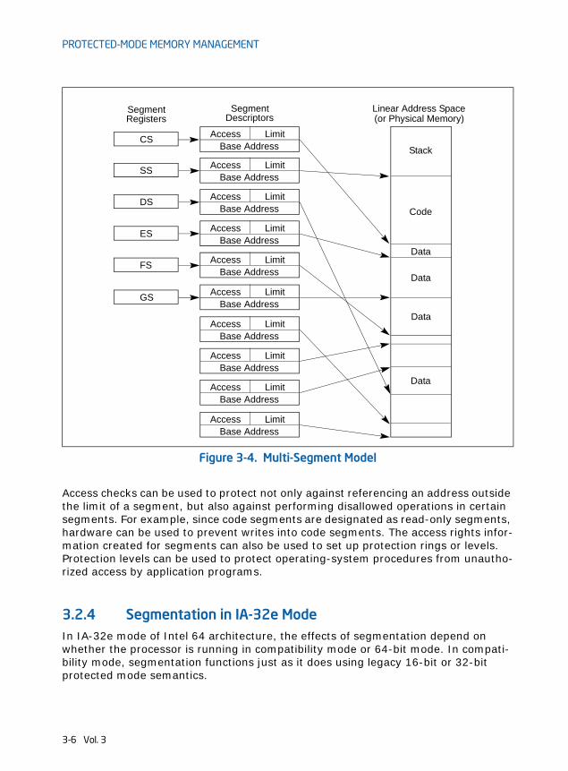
PROTECTED-MODE MEMORY MANAGEMENT
Access checks can be used to protect not only against referencing an address outside the limit of a segment, but also against performing disallowed operations in certain segments. For example, since code segments are designated as read-only segments, hardware can be used to prevent writes into code segments. The access rights infor-mation created for segments can also be used to set up protection rings or levels. Protection levels can be used to protect operating-system procedures from unautho-rized access by application programs.
3.2.4 Segmentation in IA-32e ModeIn IA-32e mode of Intel 64 architecture, the effects of segmentation depend on whether the processor is running in compatibility mode or 64-bit mode. In compati-bility mode, segmentation functions just as it does using legacy 16-bit or 32-bit protected mode semantics.
Figure 3-4. Multi-Segment Model
Linear Address Space(or Physical Memory)
SegmentRegisters
CS
SegmentDescriptors
LimitAccessBase Address
SS LimitAccessBase Address
DS LimitAccessBase Address
ES LimitAccessBase Address
FS LimitAccessBase Address
GS LimitAccessBase Address
LimitAccessBase Address
LimitAccessBase Address
LimitAccessBase Address
LimitAccessBase Address
Stack
Code
Data
Data
Data
Data
3-6 Vol. 3

PROTECTED-MODE MEMORY MANAGEMENT
In 64-bit mode, segmentation is generally (but not completely) disabled, creating a flat 64-bit linear-address space. The processor treats the segment base of CS, DS, ES, SS as zero, creating a linear address that is equal to the effective address. The FS and GS segments are exceptions. These segment registers (which hold the segment base) can be used as an additional base registers in linear address calculations. They facilitate addressing local data and certain operating system data structures.
Note that the processor does not perform segment limit checks at runtime in 64-bit mode.
3.2.5 Paging and SegmentationPaging can be used with any of the segmentation models described in Figures 3-2, 3-3, and 3-4. The processor’s paging mechanism divides the linear address space (into which segments are mapped) into pages (as shown in Figure 3-1). These linear-address-space pages are then mapped to pages in the physical address space. The paging mechanism offers several page-level protection facilities that can be used with or instead of the segment-protection facilities. For example, it lets read-write protection be enforced on a page-by-page basis. The paging mechanism also provides two-level user-supervisor protection that can also be specified on a page-by-page basis.
3.3 PHYSICAL ADDRESS SPACEIn protected mode, the IA-32 architecture provides a normal physical address space of 4 GBytes (232
bytes). This is the address space that the processor can address on its address bus. This address space is flat (unsegmented), with addresses ranging continuously from 0 to FFFFFFFFH. This physical address space can be mapped to read-write memory, read-only memory, and memory mapped I/O. The memory mapping facilities described in this chapter can be used to divide this physical memory up into segments and/or pages.
Starting with the Pentium Pro processor, the IA-32 architecture also supports an extension of the physical address space to 236 bytes (64 GBytes); with a maximum physical address of FFFFFFFFFH. This extension is invoked in either of two ways:
• Using the physical address extension (PAE) flag, located in bit 5 of control register CR4.
• Using the 36-bit page size extension (PSE-36) feature (introduced in the Pentium III processors).
Physical address support has since been extended beyond 36 bits. See Chapter 4, “Paging” for more information about 36-bit physical addressing.
Vol. 3 3-7

PROTECTED-MODE MEMORY MANAGEMENT
3.3.1 Intel® 64 Processors and Physical Address SpaceOn processors that support Intel 64 architecture (CPUID.80000001:EDX[29] = 1), the size of the physical address range is implementation-specific and indicated by CPUID.80000008H:EAX[bits 7-0].
For the format of information returned in EAX, see “CPUID—CPU Identification” in Chapter 3 of the Intel® 64 and IA-32 Architectures Software Developer’s Manual, Volume 2A. See also: Chapter 4, “Paging.”
3.4 LOGICAL AND LINEAR ADDRESSESAt the system-architecture level in protected mode, the processor uses two stages of address translation to arrive at a physical address: logical-address translation and linear address space paging.
Even with the minimum use of segments, every byte in the processor’s address space is accessed with a logical address. A logical address consists of a 16-bit segment selector and a 32-bit offset (see Figure 3-5). The segment selector identi-fies the segment the byte is located in and the offset specifies the location of the byte in the segment relative to the base address of the segment.
The processor translates every logical address into a linear address. A linear address is a 32-bit address in the processor’s linear address space. Like the physical address space, the linear address space is a flat (unsegmented), 232-byte address space, with addresses ranging from 0 to FFFFFFFFH. The linear address space contains all the segments and system tables defined for a system.
To translate a logical address into a linear address, the processor does the following:
1. Uses the offset in the segment selector to locate the segment descriptor for the segment in the GDT or LDT and reads it into the processor. (This step is needed only when a new segment selector is loaded into a segment register.)
2. Examines the segment descriptor to check the access rights and range of the segment to insure that the segment is accessible and that the offset is within the limits of the segment.
3. Adds the base address of the segment from the segment descriptor to the offset to form a linear address.
3-8 Vol. 3
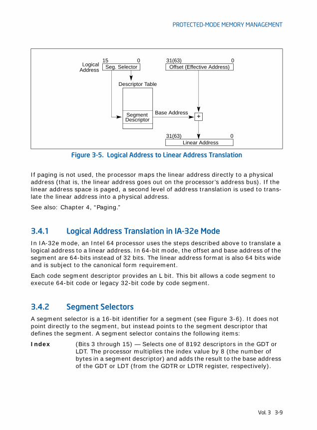
PROTECTED-MODE MEMORY MANAGEMENT
If paging is not used, the processor maps the linear address directly to a physical address (that is, the linear address goes out on the processor’s address bus). If the linear address space is paged, a second level of address translation is used to trans-late the linear address into a physical address.
See also: Chapter 4, “Paging.”
3.4.1 Logical Address Translation in IA-32e ModeIn IA-32e mode, an Intel 64 processor uses the steps described above to translate a logical address to a linear address. In 64-bit mode, the offset and base address of the segment are 64-bits instead of 32 bits. The linear address format is also 64 bits wide and is subject to the canonical form requirement.
Each code segment descriptor provides an L bit. This bit allows a code segment to execute 64-bit code or legacy 32-bit code by code segment.
3.4.2 Segment SelectorsA segment selector is a 16-bit identifier for a segment (see Figure 3-6). It does not point directly to the segment, but instead points to the segment descriptor that defines the segment. A segment selector contains the following items:
Index (Bits 3 through 15) — Selects one of 8192 descriptors in the GDT or LDT. The processor multiplies the index value by 8 (the number of bytes in a segment descriptor) and adds the result to the base address of the GDT or LDT (from the GDTR or LDTR register, respectively).
Figure 3-5. Logical Address to Linear Address Translation
Offset (Effective Address)0
Base Address
Descriptor Table
SegmentDescriptor
31(63)Seg. Selector
015Logical
Address
+
Linear Address031(63)
Vol. 3 3-9

PROTECTED-MODE MEMORY MANAGEMENT
TI (table indicator) flag(Bit 2) — Specifies the descriptor table to use: clearing this flag selects the GDT; setting this flag selects the current LDT.
Requested Privilege Level (RPL)(Bits 0 and 1) — Specifies the privilege level of the selector. The priv-ilege level can range from 0 to 3, with 0 being the most privileged level. See Section 5.5, “Privilege Levels”, for a description of the rela-tionship of the RPL to the CPL of the executing program (or task) and the descriptor privilege level (DPL) of the descriptor the segment selector points to.
The first entry of the GDT is not used by the processor. A segment selector that points to this entry of the GDT (that is, a segment selector with an index of 0 and the TI flag set to 0) is used as a “null segment selector.” The processor does not generate an exception when a segment register (other than the CS or SS registers) is loaded with a null selector. It does, however, generate an exception when a segment register holding a null selector is used to access memory. A null selector can be used to initialize unused segment registers. Loading the CS or SS register with a null segment selector causes a general-protection exception (#GP) to be generated.
Segment selectors are visible to application programs as part of a pointer variable, but the values of selectors are usually assigned or modified by link editors or linking loaders, not application programs.
3.4.3 Segment RegistersTo reduce address translation time and coding complexity, the processor provides registers for holding up to 6 segment selectors (see Figure 3-7). Each of these segment registers support a specific kind of memory reference (code, stack, or data). For virtually any kind of program execution to take place, at least the code-segment (CS), data-segment (DS), and stack-segment (SS) registers must be loaded with valid segment selectors. The processor also provides three additional data-segment registers (ES, FS, and GS), which can be used to make additional data segments available to the currently executing program (or task).
Figure 3-6. Segment Selector
15 3 2 1 0TIIndex
Table Indicator 0 = GDT 1 = LDTRequested Privilege Level (RPL)
RPL
3-10 Vol. 3
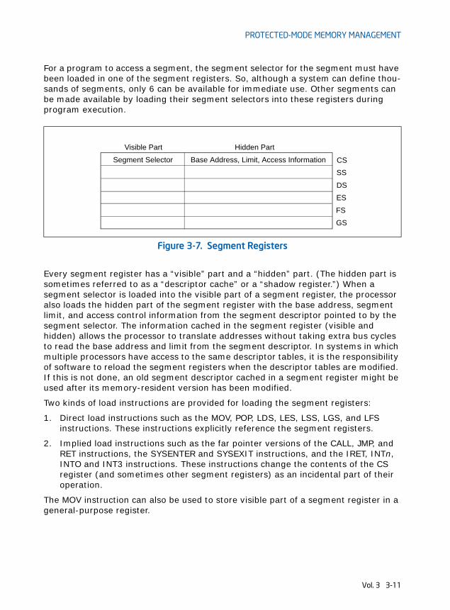
PROTECTED-MODE MEMORY MANAGEMENT
For a program to access a segment, the segment selector for the segment must have been loaded in one of the segment registers. So, although a system can define thou-sands of segments, only 6 can be available for immediate use. Other segments can be made available by loading their segment selectors into these registers during program execution.
Every segment register has a “visible” part and a “hidden” part. (The hidden part is sometimes referred to as a “descriptor cache” or a “shadow register.”) When a segment selector is loaded into the visible part of a segment register, the processor also loads the hidden part of the segment register with the base address, segment limit, and access control information from the segment descriptor pointed to by the segment selector. The information cached in the segment register (visible and hidden) allows the processor to translate addresses without taking extra bus cycles to read the base address and limit from the segment descriptor. In systems in which multiple processors have access to the same descriptor tables, it is the responsibility of software to reload the segment registers when the descriptor tables are modified. If this is not done, an old segment descriptor cached in a segment register might be used after its memory-resident version has been modified.
Two kinds of load instructions are provided for loading the segment registers:
1. Direct load instructions such as the MOV, POP, LDS, LES, LSS, LGS, and LFS instructions. These instructions explicitly reference the segment registers.
2. Implied load instructions such as the far pointer versions of the CALL, JMP, and RET instructions, the SYSENTER and SYSEXIT instructions, and the IRET, INTn, INTO and INT3 instructions. These instructions change the contents of the CS register (and sometimes other segment registers) as an incidental part of their operation.
The MOV instruction can also be used to store visible part of a segment register in a general-purpose register.
Figure 3-7. Segment Registers
CSSS
DSES
FSGS
Segment Selector Base Address, Limit, Access Information
Visible Part Hidden Part
Vol. 3 3-11

PROTECTED-MODE MEMORY MANAGEMENT
3.4.5 Segment DescriptorsA segment descriptor is a data structure in a GDT or LDT that provides the processor with the size and location of a segment, as well as access control and status informa-tion. Segment descriptors are typically created by compilers, linkers, loaders, or the operating system or executive, but not application programs. Figure 3-8 illustrates the general descriptor format for all types of segment descriptors.
The flags and fields in a segment descriptor are as follows:
Segment limit fieldSpecifies the size of the segment. The processor puts together the two segment limit fields to form a 20-bit value. The processor inter-prets the segment limit in one of two ways, depending on the setting of the G (granularity) flag:
• If the granularity flag is clear, the segment size can range from 1 byte to 1 MByte, in byte increments.
• If the granularity flag is set, the segment size can range from 4 KBytes to 4 GBytes, in 4-KByte increments.
The processor uses the segment limit in two different ways, depending on whether the segment is an expand-up or an expand-down segment. See Section 3.4.5.1, “Code- and Data-Segment Descriptor Types”, for more information about segment types. For expand-up segments, the offset in a logical address can range from 0
Figure 3-8. Segment Descriptor
31 24 23 22 21 20 19 16 15 1314 12 11 8 7 0
PBase 31:24 GDPL
TypeSL 4
31 16 15 0
Base Address 15:00 Segment Limit 15:00 0
Base 23:16D/B
AVL
Seg.Limit19:16
G — GranularityLIMIT — Segment LimitP — Segment presentS — Descriptor type (0 = system; 1 = code or data)TYPE — Segment type
DPL — Descriptor privilege level
AVL — Available for use by system softwareBASE — Segment base addressD/B — Default operation size (0 = 16-bit segment; 1 = 32-bit segment)
L — 64-bit code segment (IA-32e mode only)
Vol. 3 3-13

PROTECTED-MODE MEMORY MANAGEMENT
to the segment limit. Offsets greater than the segment limit generate general-protection exceptions (#GP). For expand-down segments, the segment limit has the reverse function; the offset can range from the segment limit to FFFFFFFFH or FFFFH, depending on the setting of the B flag. Offsets less than the segment limit generate general-protection exceptions. Decreasing the value in the segment limit field for an expand-down segment allocates new memory at the bottom of the segment's address space, rather than at the top. IA-32 architec-ture stacks always grow downwards, making this mechanism conve-nient for expandable stacks.
Base address fieldsDefines the location of byte 0 of the segment within the 4-GByte linear address space. The processor puts together the three base address fields to form a single 32-bit value. Segment base addresses should be aligned to 16-byte boundaries. Although 16-byte alignment is not required, this alignment allows programs to maximize perfor-mance by aligning code and data on 16-byte boundaries.
Type field Indicates the segment or gate type and specifies the kinds of access that can be made to the segment and the direction of growth. The interpretation of this field depends on whether the descriptor type flag specifies an application (code or data) descriptor or a system descriptor. The encoding of the type field is different for code, data, and system descriptors (see Figure 5-1). See Section 3.4.5.1, “Code- and Data-Segment Descriptor Types”, for a description of how this field is used to specify code and data-segment types.
S (descriptor type) flagSpecifies whether the segment descriptor is for a system segment (S flag is clear) or a code or data segment (S flag is set).
DPL (descriptor privilege level) fieldSpecifies the privilege level of the segment. The privilege level can range from 0 to 3, with 0 being the most privileged level. The DPL is used to control access to the segment. See Section 5.5, “Privilege Levels”, for a description of the relationship of the DPL to the CPL of the executing code segment and the RPL of a segment selector.
P (segment-present) flagIndicates whether the segment is present in memory (set) or not present (clear). If this flag is clear, the processor generates a segment-not-present exception (#NP) when a segment selector that points to the segment descriptor is loaded into a segment register. Memory management software can use this flag to control which segments are actually loaded into physical memory at a given time. It offers a control in addition to paging for managing virtual memory.
Figure 3-9 shows the format of a segment descriptor when the segment-present flag is clear. When this flag is clear, the operating system or executive is free to use the locations marked “Available” to
3-14 Vol. 3

PROTECTED-MODE MEMORY MANAGEMENT
store its own data, such as information regarding the whereabouts of the missing segment.
D/B (default operation size/default stack pointer size and/or upper bound) flagPerforms different functions depending on whether the segment descriptor is an executable code segment, an expand-down data segment, or a stack segment. (This flag should always be set to 1 for 32-bit code and data segments and to 0 for 16-bit code and data segments.)
• Executable code segment. The flag is called the D flag and it indicates the default length for effective addresses and operands referenced by instructions in the segment. If the flag is set, 32-bit addresses and 32-bit or 8-bit operands are assumed; if it is clear, 16-bit addresses and 16-bit or 8-bit operands are assumed. The instruction prefix 66H can be used to select an operand size other than the default, and the prefix 67H can be used select an address size other than the default.
• Stack segment (data segment pointed to by the SS register). The flag is called the B (big) flag and it specifies the size of the stack pointer used for implicit stack operations (such as pushes, pops, and calls). If the flag is set, a 32-bit stack pointer is used, which is stored in the 32-bit ESP register; if the flag is clear, a 16-bit stack pointer is used, which is stored in the 16-bit SP register. If the stack segment is set up to be an expand-down data segment (described in the next paragraph), the B flag also specifies the upper bound of the stack segment.
• Expand-down data segment. The flag is called the B flag and it specifies the upper bound of the segment. If the flag is set, the upper bound is FFFFFFFFH (4 GBytes); if the flag is clear, the upper bound is FFFFH (64 KBytes).
Figure 3-9. Segment Descriptor When Segment-Present Flag Is Clear
31 16 15 1314 12 11 8 7 0
0AvailableDPL
TypeS 4
31 0
Available 0
Available
Vol. 3 3-15

PROTECTED-MODE MEMORY MANAGEMENT
G (granularity) flagDetermines the scaling of the segment limit field. When the granu-larity flag is clear, the segment limit is interpreted in byte units; when flag is set, the segment limit is interpreted in 4-KByte units. (This flag does not affect the granularity of the base address; it is always byte granular.) When the granularity flag is set, the twelve least significant bits of an offset are not tested when checking the offset against the segment limit. For example, when the granularity flag is set, a limit of 0 results in valid offsets from 0 to 4095.
L (64-bit code segment) flagIn IA-32e mode, bit 21 of the second doubleword of the segment descriptor indicates whether a code segment contains native 64-bit code. A value of 1 indicates instructions in this code segment are executed in 64-bit mode. A value of 0 indicates the instructions in this code segment are executed in compatibility mode. If L-bit is set, then D-bit must be cleared. When not in IA-32e mode or for non-code segments, bit 21 is reserved and should always be set to 0.
Available and reserved bitsBit 20 of the second doubleword of the segment descriptor is available for use by system software.
3.4.5.1 Code- and Data-Segment Descriptor TypesWhen the S (descriptor type) flag in a segment descriptor is set, the descriptor is for either a code or a data segment. The highest order bit of the type field (bit 11 of the second double word of the segment descriptor) then determines whether the descriptor is for a data segment (clear) or a code segment (set).
For data segments, the three low-order bits of the type field (bits 8, 9, and 10) are interpreted as accessed (A), write-enable (W), and expansion-direction (E). See Table 3-1 for a description of the encoding of the bits in the type field for code and data segments. Data segments can be read-only or read/write segments, depending on the setting of the write-enable bit.
3-16 Vol. 3

PROTECTED-MODE MEMORY MANAGEMENT
Stack segments are data segments which must be read/write segments. Loading the SS register with a segment selector for a nonwritable data segment generates a general-protection exception (#GP). If the size of a stack segment needs to be changed dynamically, the stack segment can be an expand-down data segment (expansion-direction flag set). Here, dynamically changing the segment limit causes stack space to be added to the bottom of the stack. If the size of a stack segment is intended to remain static, the stack segment may be either an expand-up or expand-down type.
The accessed bit indicates whether the segment has been accessed since the last time the operating-system or executive cleared the bit. The processor sets this bit whenever it loads a segment selector for the segment into a segment register, assuming that the type of memory that contains the segment descriptor supports processor writes. The bit remains set until explicitly cleared. This bit can be used both for virtual memory management and for debugging.
Table 3-1. Code- and Data-Segment Types
Type Field DescriptorType
Description
Decimal 11 10E
9W
8A
0 0 0 0 0 Data Read-Only
1 0 0 0 1 Data Read-Only, accessed
2 0 0 1 0 Data Read/Write
3 0 0 1 1 Data Read/Write, accessed
4 0 1 0 0 Data Read-Only, expand-down
5 0 1 0 1 Data Read-Only, expand-down, accessed
6 0 1 1 0 Data Read/Write, expand-down
7 0 1 1 1 Data Read/Write, expand-down, accessed
C R A
8 1 0 0 0 Code Execute-Only
9 1 0 0 1 Code Execute-Only, accessed
10 1 0 1 0 Code Execute/Read
11 1 0 1 1 Code Execute/Read, accessed
12 1 1 0 0 Code Execute-Only, conforming
13 1 1 0 1 Code Execute-Only, conforming, accessed
14 1 1 1 0 Code Execute/Read, conforming
15 1 1 1 1 Code Execute/Read, conforming, accessed
Vol. 3 3-17

PROTECTED-MODE MEMORY MANAGEMENT
For code segments, the three low-order bits of the type field are interpreted as accessed (A), read enable (R), and conforming (C). Code segments can be execute-only or execute/read, depending on the setting of the read-enable bit. An execute/read segment might be used when constants or other static data have been placed with instruction code in a ROM. Here, data can be read from the code segment either by using an instruction with a CS override prefix or by loading a segment selector for the code segment in a data-segment register (the DS, ES, FS, or GS registers). In protected mode, code segments are not writable.
Code segments can be either conforming or nonconforming. A transfer of execution into a more-privileged conforming segment allows execution to continue at the current privilege level. A transfer into a nonconforming segment at a different privi-lege level results in a general-protection exception (#GP), unless a call gate or task gate is used (see Section 5.8.1, “Direct Calls or Jumps to Code Segments”, for more information on conforming and nonconforming code segments). System utilities that do not access protected facilities and handlers for some types of exceptions (such as, divide error or overflow) may be loaded in conforming code segments. Utilities that need to be protected from less privileged programs and procedures should be placed in nonconforming code segments.
NOTEExecution cannot be transferred by a call or a jump to a less-privileged (numerically higher privilege level) code segment, regardless of whether the target segment is a conforming or noncon-forming code segment. Attempting such an execution transfer will result in a general-protection exception.
All data segments are nonconforming, meaning that they cannot be accessed by less privileged programs or procedures (code executing at numerically high privilege levels). Unlike code segments, however, data segments can be accessed by more privileged programs or procedures (code executing at numerically lower privilege levels) without using a special access gate.
If the segment descriptors in the GDT or an LDT are placed in ROM, the processor can enter an indefinite loop if software or the processor attempts to update (write to) the ROM-based segment descriptors. To prevent this problem, set the accessed bits for all segment descriptors placed in a ROM. Also, remove operating-system or executive code that attempts to modify segment descriptors located in ROM.
3.5 SYSTEM DESCRIPTOR TYPESWhen the S (descriptor type) flag in a segment descriptor is clear, the descriptor type is a system descriptor. The processor recognizes the following types of system descriptors:
• Local descriptor-table (LDT) segment descriptor.
3-18 Vol. 3

PROTECTED-MODE MEMORY MANAGEMENT
• Task-state segment (TSS) descriptor.
• Call-gate descriptor.
• Interrupt-gate descriptor.
• Trap-gate descriptor.
• Task-gate descriptor.
These descriptor types fall into two categories: system-segment descriptors and gate descriptors. System-segment descriptors point to system segments (LDT and TSS segments). Gate descriptors are in themselves “gates,” which hold pointers to proce-dure entry points in code segments (call, interrupt, and trap gates) or which hold segment selectors for TSS’s (task gates).
Table 3-2 shows the encoding of the type field for system-segment descriptors and gate descriptors. Note that system descriptors in IA-32e mode are 16 bytes instead of 8 bytes.
Table 3-2. System-Segment and Gate-Descriptor Types
Type Field Description
Decimal 11 10 9 8 32-Bit Mode IA-32e Mode
0 0 0 0 0 Reserved Upper 8 byte of an 16-byte descriptor
1 0 0 0 1 16-bit TSS (Available) Reserved
2 0 0 1 0 LDT LDT
3 0 0 1 1 16-bit TSS (Busy) Reserved
4 0 1 0 0 16-bit Call Gate Reserved
5 0 1 0 1 Task Gate Reserved
6 0 1 1 0 16-bit Interrupt Gate Reserved
7 0 1 1 1 16-bit Trap Gate Reserved
8 1 0 0 0 Reserved Reserved
9 1 0 0 1 32-bit TSS (Available) 64-bit TSS (Available)
10 1 0 1 0 Reserved Reserved
11 1 0 1 1 32-bit TSS (Busy) 64-bit TSS (Busy)
12 1 1 0 0 32-bit Call Gate 64-bit Call Gate
13 1 1 0 1 Reserved Reserved
14 1 1 1 0 32-bit Interrupt Gate 64-bit Interrupt Gate
15 1 1 1 1 32-bit Trap Gate 64-bit Trap Gate
Vol. 3 3-19
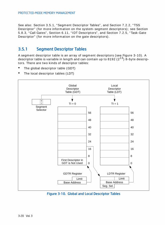
PROTECTED-MODE MEMORY MANAGEMENT
See also: Section 3.5.1, “Segment Descriptor Tables”, and Section 7.2.2, “TSS Descriptor” (for more information on the system-segment descriptors); see Section 5.8.3, “Call Gates”, Section 6.11, “IDT Descriptors”, and Section 7.2.5, “Task-Gate Descriptor” (for more information on the gate descriptors).
3.5.1 Segment Descriptor TablesA segment descriptor table is an array of segment descriptors (see Figure 3-10). A descriptor table is variable in length and can contain up to 8192 (213) 8-byte descrip-tors. There are two kinds of descriptor tables:
• The global descriptor table (GDT)
• The local descriptor tables (LDT)
Figure 3-10. Global and Local Descriptor Tables
SegmentSelector
GlobalDescriptor
T
First Descriptor inGDT is Not Used
TI = 0I
56
40
48
32
24
16
8
0
TI = 1
56
40
48
32
24
16
8
0
Table (GDT)
LocalDescriptor
Table (LDT)
Base AddressLimit
GDTR Register LDTR Register
Base AddressSeg. Sel.
Limit
3-20 Vol. 3

PROTECTED-MODE MEMORY MANAGEMENT
Each system must have one GDT defined, which may be used for all programs and tasks in the system. Optionally, one or more LDTs can be defined. For example, an LDT can be defined for each separate task being run, or some or all tasks can share the same LDT.
The GDT is not a segment itself; instead, it is a data structure in linear address space. The base linear address and limit of the GDT must be loaded into the GDTR register (see Section 2.4, “Memory-Management Registers”). The base addresses of the GDT should be aligned on an eight-byte boundary to yield the best processor perfor-mance. The limit value for the GDT is expressed in bytes. As with segments, the limit value is added to the base address to get the address of the last valid byte. A limit value of 0 results in exactly one valid byte. Because segment descriptors are always 8 bytes long, the GDT limit should always be one less than an integral multiple of eight (that is, 8N – 1).
The first descriptor in the GDT is not used by the processor. A segment selector to this “null descriptor” does not generate an exception when loaded into a data-segment register (DS, ES, FS, or GS), but it always generates a general-protection exception (#GP) when an attempt is made to access memory using the descriptor. By initializing the segment registers with this segment selector, accidental reference to unused segment registers can be guaranteed to generate an exception.
The LDT is located in a system segment of the LDT type. The GDT must contain a segment descriptor for the LDT segment. If the system supports multiple LDTs, each must have a separate segment selector and segment descriptor in the GDT. The segment descriptor for an LDT can be located anywhere in the GDT. See Section 3.5, “System Descriptor Types”, information on the LDT segment-descriptor type.
An LDT is accessed with its segment selector. To eliminate address translations when accessing the LDT, the segment selector, base linear address, limit, and access rights of the LDT are stored in the LDTR register (see Section 2.4, “Memory-Management Registers”).
When the GDTR register is stored (using the SGDT instruction), a 48-bit “pseudo-descriptor” is stored in memory (see top diagram in Figure 3-11). To avoid alignment check faults in user mode (privilege level 3), the pseudo-descriptor should be located at an odd word address (that is, address MOD 4 is equal to 2). This causes the processor to store an aligned word, followed by an aligned doubleword. User-mode programs normally do not store pseudo-descriptors, but the possibility of generating an alignment check fault can be avoided by aligning pseudo-descriptors in this way. The same alignment should be used when storing the IDTR register using the SIDT instruction. When storing the LDTR or task register (using the SLTR or STR instruc-tion, respectively), the pseudo-descriptor should be located at a doubleword address (that is, address MOD 4 is equal to 0).
Vol. 3 3-21

PROTECTED-MODE MEMORY MANAGEMENT
3.5.2 Segment Descriptor Tables in IA-32e ModeIn IA-32e mode, a segment descriptor table can contain up to 8192 (213) 8-byte descriptors. An entry in the segment descriptor table can be 8 bytes. System descrip-tors are expanded to 16 bytes (occupying the space of two entries).
GDTR and LDTR registers are expanded to hold 64-bit base address. The corre-sponding pseudo-descriptor is 80 bits. (see the bottom diagram in Figure 3-11).
The following system descriptors expand to 16 bytes:
— Call gate descriptors (see Section 5.8.3.1, “IA-32e Mode Call Gates”)
— IDT gate descriptors (see Section 6.14.1, “64-Bit Mode IDT”)
— LDT and TSS descriptors (see Section 7.2.3, “TSS Descriptor in 64-bit mode”).
Figure 3-11. Pseudo-Descriptor Formats
032-bit Base Address Limit
47 1516
064-bit Base Address Limit
79 1516
3-22 Vol. 3

CHAPTER 4PAGING
Chapter 3 explains how segmentation converts logical addresses to linear addresses. Paging (or linear-address translation) is the process of translating linear addresses so that they can be used to access memory or I/O devices. Paging translates each linear address to a physical address and determines, for each translation, what accesses to the linear address are allowed (the address’s access rights) and the type of caching used for such accesses (the address’s memory type).
Intel-64 processors support three different paging modes. These modes are identi-fied and defined in Section 4.1. Section 4.2 gives an overview of the translation mechanism that is used in all modes. Section 4.3, Section 4.4, and Section 4.5 discuss the three paging modes in detail.
Section 4.6 details how paging determines and uses access rights. Section 4.7 discusses exceptions that may be generated by paging (page-fault exceptions). Section 4.8 considers data which the processor writes in response to linear-address accesses (accessed and dirty flags).
Section 4.9 describes how paging determines the memory types used for accesses to linear addresses. Section 4.10 provides details of how a processor may cache infor-mation about linear-address translation. Section 4.11 outlines interactions between paging and certain VMX features. Section 4.12 gives an overview of how paging can be used to implement virtual memory.
4.1 PAGING MODES AND CONTROL BITSPaging behavior is controlled by the following control bits:
• The WP and PG flags in control register CR0 (bit 16 and bit 31, respectively).
• The PSE, PAE, PGE, and PCIDE flags in control register CR4 (bit 4, bit 5, bit 7, and bit 17, respectively).
• The LME and NXE flags in the IA32_EFER MSR (bit 8 and bit 11, respectively).
Software enables paging by using the MOV to CR0 instruction to set CR0.PG. Before doing so, software should ensure that control register CR3 contains the physical address of the first paging structure that the processor will use for linear-address translation (see Section 4.2) and that structure is initialized as desired. See Table 4-3, Table 4-7, and Table 4-12 for the use of CR3 in the different paging modes.
Section 4.1.1 describes how the values of CR0.PG, CR4.PAE, and IA32_EFER.LME determine whether paging is in use and, if so, which of three paging modes is in use. Section 4.1.2 explains how to manage these bits to establish or make changes in
Vol. 3 4-1

PAGING
paging modes. Section 4.1.3 discusses how CR0.WP, CR4.PSE, CR4.PGE, CR4.PCIDE, and IA32_EFER.NXE modify the operation of the different paging modes.
4.1.1 Three Paging ModesIf CR0.PG = 0, paging is not used. The logical processor treats all linear addresses as if they were physical addresses. CR4.PAE and IA32_EFER.LME are ignored by the processor, as are CR0.WP, CR4.PSE, and CR4.PGE, and IA32_EFER.NXE.
Paging is enabled if CR0.PG = 1. Paging can be enabled only if protection is enabled (CR0.PE = 1). If paging is enabled, one of three paging modes is used. The values of CR4.PAE and IA32_EFER.LME determine which paging mode is used:
• If CR0.PG = 1 and CR4.PAE = 0, 32-bit paging is used. 32-bit paging is detailed in Section 4.3. 32-bit paging uses CR0.WP, CR4.PSE, and CR4.PGE as described in Section 4.1.3.
• If CR0.PG = 1, CR4.PAE = 1, and IA32_EFER.LME = 0, PAE paging is used. PAE paging is detailed in Section 4.4. PAE paging uses CR0.WP, CR4.PGE, and IA32_EFER.NXE as described in Section 4.1.3.
• If CR0.PG = 1, CR4.PAE = 1, and IA32_EFER.LME = 1, IA-32e paging is used.1 IA-32e paging is detailed in Section 4.5. IA-32e paging uses CR0.WP, CR4.PGE, CR4.PCIDE, and IA32_EFER.NXE as described in Section 4.1.3. IA-32e paging is available only on processors that support the Intel 64 architecture.
The three paging modes differ with regard to the following details:
• Linear-address width. The size of the linear addresses that can be translated.
• Physical-address width. The size of the physical addresses produced by paging.
• Page size. The granularity at which linear addresses are translated. Linear addresses on the same page are translated to corresponding physical addresses on the same page.
• Support for execute-disable access rights. In some paging modes, software can be prevented from fetching instructions from pages that are otherwise readable.
Table 4-1 illustrates the key differences between the three paging modes.
Because they are used only if IA32_EFER.LME = 0, 32-bit paging and PAE paging is used only in legacy protected mode. Because legacy protected mode cannot produce
1. The LMA flag in the IA32_EFER MSR (bit 10) is a status bit that indicates whether the logical pro-cessor is in IA-32e mode (and thus using IA-32e paging). The processor always sets IA32_EFER.LMA to CR0.PG & IA32_EFER.LME. Software cannot directly modify IA32_EFER.LMA; an execution of WRMSR to the IA32_EFER MSR ignores bit 10 of its source operand.
4-2 Vol. 3
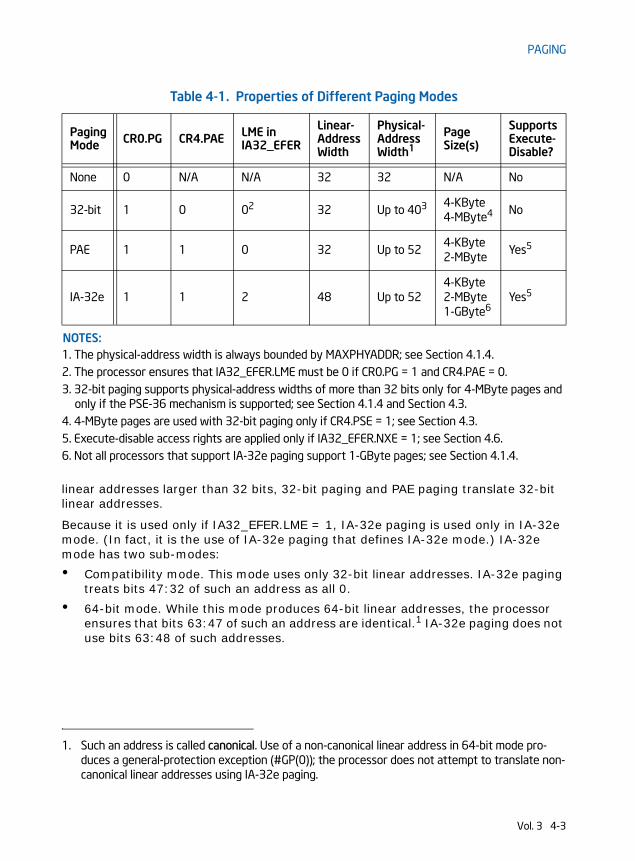
PAGING
linear addresses larger than 32 bits, 32-bit paging and PAE paging translate 32-bit linear addresses.
Because it is used only if IA32_EFER.LME = 1, IA-32e paging is used only in IA-32e mode. (In fact, it is the use of IA-32e paging that defines IA-32e mode.) IA-32e mode has two sub-modes:
• Compatibility mode. This mode uses only 32-bit linear addresses. IA-32e paging treats bits 47:32 of such an address as all 0.
• 64-bit mode. While this mode produces 64-bit linear addresses, the processor ensures that bits 63:47 of such an address are identical.1 IA-32e paging does not use bits 63:48 of such addresses.
Table 4-1. Properties of Different Paging Modes
PagingMode CR0.PG CR4.PAE LME in
IA32_EFER
Linear-AddressWidth
Physical-AddressWidth1
PageSize(s)
SupportsExecute-Disable?
None 0 N/A N/A 32 32 N/A No
32-bit 1 0 02 32 Up to 403 4-KByte4-MByte4 No
PAE 1 1 0 32 Up to 524-KByte2-MByte
Yes5
IA-32e 1 1 2 48 Up to 524-KByte2-MByte1-GByte6
Yes5
NOTES:1. The physical-address width is always bounded by MAXPHYADDR; see Section 4.1.4.2. The processor ensures that IA32_EFER.LME must be 0 if CR0.PG = 1 and CR4.PAE = 0.3. 32-bit paging supports physical-address widths of more than 32 bits only for 4-MByte pages and
only if the PSE-36 mechanism is supported; see Section 4.1.4 and Section 4.3.4. 4-MByte pages are used with 32-bit paging only if CR4.PSE = 1; see Section 4.3.5. Execute-disable access rights are applied only if IA32_EFER.NXE = 1; see Section 4.6.6. Not all processors that support IA-32e paging support 1-GByte pages; see Section 4.1.4.
1. Such an address is called canonical. Use of a non-canonical linear address in 64-bit mode pro-duces a general-protection exception (#GP(0)); the processor does not attempt to translate non-canonical linear addresses using IA-32e paging.
Vol. 3 4-3

PAGING
• Page1GB: 1-GByte pages.If CPUID.80000001H:EDX.Page1GB [bit 26] = 1, 1-GByte pages are supported with IA-32e paging (see Section 4.5).
• LM: IA-32e mode support.If CPUID.80000001H:EDX.LM [bit 29] = 1, IA32_EFER.LME may be set to 1, enabling IA-32e paging. (Processors that do not support CPUID function 80000001H do not allow IA32_EFER.LME to be set to 1.)
• CPUID.80000008H:EAX[7:0] reports the physical-address width supported by the processor. (For processors that do not support CPUID function 80000008H, the width is generally 36 if CPUID.01H:EDX.PAE [bit 6] = 1 and 32 otherwise.) This width is referred to as MAXPHYADDR. MAXPHYADDR is at most 52.
• CPUID.80000008H:EAX[15:8] reports the linear-address width supported by the processor. Generally, this value is 48 if CPUID.80000001H:EDX.LM [bit 29] = 1 and 32 otherwise. (Processors that do not support CPUID function 80000008H, support a linear-address width of 32.)
4.2 HIERARCHICAL PAGING STRUCTURES: AN OVERVIEWAll three paging modes translate linear addresses use hierarchical paging struc-tures. This section provides an overview of their operation. Section 4.3, Section 4.4, and Section 4.5 provide details for the three paging modes.
Every paging structure is 4096 Bytes in size and comprises a number of individual entries. With 32-bit paging, each entry is 32 bits (4 bytes); there are thus 1024 entries in each structure. With PAE paging and IA-32e paging, each entry is 64 bits (8 bytes); there are thus 512 entries in each structure. (PAE paging includes one exception, a paging structure that is 32 bytes in size, containing 4 64-bit entries.)
The processor uses the upper portion of a linear address to identify a series of paging-structure entries. The last of these entries identifies the physical address of the region to which the linear address translates (called the page frame). The lower portion of the linear address (called the page offset) identifies the specific address within that region to which the linear address translates.
Each paging-structure entry contains a physical address, which is either the address of another paging structure or the address of a page frame. In the first case, the entry is said to reference the other paging structure; in the latter, the entry is said to map a page.
The first paging structure used for any translation is located at the physical address in CR3. A linear address is translated using the following iterative procedure. A portion of the linear address (initially the uppermost bits) select an entry in a paging structure (initially the one located using CR3). If that entry references another paging structure, the process continues with that paging structure and with the portion of the linear address immediately below that just used. If instead the entry maps a page, the process completes: the physical address in the entry is that of the page frame and the remaining lower portion of the linear address is the page offset.
Vol. 3 4-7

PAGING
The following items give an example for each of the three paging modes (each example locates a 4-KByte page frame):
• With 32-bit paging, each paging structure comprises 1024 = 210 entries. For this reason, the translation process uses 10 bits at a time from a 32-bit linear address. Bits 31:22 identify the first paging-structure entry and bits 21:12 identify a second. The latter identifies the page frame. Bits 11:0 of the linear address are the page offset within the 4-KByte page frame. (See Figure 4-2 for an illustration.)
• With PAE paging, the first paging structure comprises only 4 = 22 entries. Translation thus begins by using bits 31:30 from a 32-bit linear address to identify the first paging-structure entry. Other paging structures comprise 512 =29 entries, so the process continues by using 9 bits at a time. Bits 29:21 identify a second paging-structure entry and bits 20:12 identify a third. This last identifies the page frame. (See Figure 4-5 for an illustration.)
• With IA-32e paging, each paging structure comprises 512 = 29 entries and translation uses 9 bits at a time from a 48-bit linear address. Bits 47:39 identify the first paging-structure entry, bits 38:30 identify a second, bits 29:21 a third, and bits 20:12 identify a fourth. Again, the last identifies the page frame. (See Figure 4-8 for an illustration.)
The translation process in each of the examples above completes by identifying a page frame. However, the paging structures may be configured so that translation terminates before doing so. This occurs if process encounters a paging-structure entry that is marked “not present” (because its P flag — bit 0 — is clear) or in which a reserved bit is set. In this case, there is no translation for the linear address; an access to that address causes a page-fault exception (see Section 4.7).
In the examples above, a paging-structure entry maps a page with 4-KByte page frame when only 12 bits remain in the linear address; entries identified earlier always reference other paging structures. That may not apply in other cases. The following items identify when an entry maps a page and when it references another paging structure:
• If more than 12 bits remain in the linear address, bit 7 (PS — page size) of the current paging-structure entry is consulted. If the bit is 0, the entry references another paging structure; if the bit is 1, the entry maps a page.
• If only 12 bits remain in the linear address, the current paging-structure entry always maps a page (bit 7 is used for other purposes).
If a paging-structure entry maps a page when more than 12 bits remain in the linear address, the entry identifies a page frame larger than 4 KBytes. For example, 32-bit paging uses the upper 10 bits of a linear address to locate the first paging-structure entry; 22 bits remain. If that entry maps a page, the page frame is 222 Bytes = 4 MBytes. 32-bit paging supports 4-MByte pages if CR4.PSE = 1. PAE paging and IA-32e paging support 2-MByte pages (regardless of the value of CR4.PSE). IA-32e paging may support 1-GByte pages (see Section 4.1.4).
Paging structures are given different names based their uses in the translation process. Table 4-2 gives the names of the different paging structures. It also
4-8 Vol. 3

PAGING
provides, for each structure, the source of the physical address used to locate it (CR3 or a different paging-structure entry); the bits in the linear address used to select an entry from the structure; and details of about whether and how such an entry can map a page.
4.3 32-BIT PAGINGA logical processor uses 32-bit paging if CR0.PG = 1 and CR4.PAE = 0. 32-bit paging translates 32-bit linear addresses to 40-bit physical addresses.1 Although 40 bits
Table 4-2. Paging Structures in the Different Paging Modes
Paging Structure
Entry Name Paging Mode
Physical Address of Structure
Bits Selecting Entry
Page Mapping
PML4 table PML4E32-bit, PAE N/A
IA-32e CR3 47:39 N/A (PS must be 0)
Page-directory-pointer table
PDPTE
32-bit N/A
PAE CR3 31:30 N/A (PS must be 0)
IA-32e PML4E 38:30 1-GByte page if PS=11
NOTES:1. Not all processors allow the PS flag to be 1 in PDPTEs; see Section 4.1.4 for how to determine
whether 1-GByte pages are supported.
Page directory PDE32-bit CR3 31:22 4-MByte page if PS=12
2. 32-bit paging ignores the PS flag in a PDE (and uses the entry to reference a page table) unless CR4.PSE = 1. Not all processors allow CR4.PSE to be 1; see Section 4.1.4 for how to determine whether 4-MByte pages are supported with 32-bit paging.
PAE, IA-32e PDPTE 29:21 2-MByte page if PS=1
Page table PTE32-bit
PDE21:12 4-KByte page
PAE, IA-32e 20:12 4-KByte page
1. Bits in the range 39:32 are 0 in any physical address used by 32-bit paging except those used to map 4-MByte pages. If the processor does not support the PSE-36 mechanism, this is true also for physical addresses used to map 4-MByte pages. If the processor does support the PSE-36 mechanism and MAXPHYADDR < 40, bits in the range 39:MAXPHYADDR are 0 in any physical address used to map a 4-MByte page. (The corresponding bits are reserved in PDEs.) See Section 4.1.4 for how to determine MAXPHYADDR and whether the PSE-36 mechanism is supported.
Vol. 3 4-9

PAGING
corresponds to 1 TByte, linear addresses are limited to 32 bits; at most 4 GBytes of linear-address space may be accessed at any given time.
32-bit paging uses a hierarchy of paging structures to produce a translation for a linear address. CR3 is used to locate the first paging-structure, the page directory. Table 4-3 illustrates how CR3 is used with 32-bit paging.
32-bit paging may map linear addresses to either 4-KByte pages or 4-MByte pages. Figure 4-2 illustrates the translation process when it uses a 4-KByte page; Figure 4-3 covers the case of a 4-MByte page. The following items describe the 32-bit paging process in more detail as well has how the page size is determined:
• A 4-KByte naturally aligned page directory is located at the physical address specified in bits 31:12 of CR3 (see Table 4-3). A page directory comprises 1024 32-bit entries (PDEs). A PDE is selected using the physical address defined as follows:
— Bits 39:32 are all 0.
— Bits 31:12 are from CR3.
— Bits 11:2 are bits 31:22 of the linear address.
— Bits 1:0 are 0.
Because a PDE is identified using bits 31:22 of the linear address, it controls access to a 4-Mbyte region of the linear-address space. Use of the PDE depends on CR.PSE and the PDE’s PS flag (bit 7):
• If CR4.PSE = 1 and the PDE’s PS flag is 1, the PDE maps a 4-MByte page (see Table 4-4). The final physical address is computed as follows:
— Bits 39:32 are bits 20:13 of the PDE.
Table 4-3. Use of CR3 with 32-Bit Paging
Bit Position(s)
Contents
2:0 Ignored
3 (PWT) Page-level write-through; indirectly determines the memory type used to access the page directory during linear-address translation (see Section 4.9)
4 (PCD) Page-level cache disable; indirectly determines the memory type used to access the page directory during linear-address translation (see Section 4.9)
11:5 Ignored
31:12 Physical address of the 4-KByte aligned page directory used for linear-address translation
63:32 Ignored (these bits exist only on processors supporting the Intel-64 architecture)
4-10 Vol. 3

PAGING
— Bits 31:22 are bits 31:22 of the PDE.1
— Bits 21:0 are from the original linear address.
Figure 4-2. Linear-Address Translation to a 4-KByte Page using 32-Bit Paging
Figure 4-3. Linear-Address Translation to a 4-MByte Page using 32-Bit Paging
1. The upper bits in the final physical address do not all come from corresponding positions in the PDE; the physical-address bits in the PDE are not all contiguous.
0Directory Table Offset
Page Directory
PDE with PS=0
CR3
Page Table
PTE
4-KByte Page
Physical Address
31 21 111222Linear Address
32
10
12
10
20
20
0Directory Offset
Page Directory
PDE with PS=1
CR3
4-MByte Page
Physical Address
31 2122Linear Address
10
22
32
18
Vol. 3 4-11

PAGING
— VM entries allow transitions from IA-32e paging directly to either 32-bit paging or PAE paging.
— VM exits allow transitions from either 32-bit paging or PAE paging directly to IA-32e paging.
• VMX transitions that result in PAE paging load the PDPTE registers (see Section 4.4.1) as follows:
— VM entries load the PDPTE registers either from the physical address being loaded into CR3 or from the virtual-machine control structure (VMCS); see Section 23.3.2.4.
— VM exits load the PDPTE registers from the physical address being loaded into CR3; see Section 24.5.4.
• VMX transitions invalidate the TLBs and paging-structure caches based on certain control settings. See Section 23.3.2.5 and Section 24.5.5 in the Intel® 64 and IA-32 Architectures Software Developer’s Manual, Volume 3B.
4.11.2 VMX Support for Address TranslationChapter 25, “VMX Support for Address Translation,” in the Intel® 64 and IA-32 Archi-tectures Software Developer’s Manual, Volume 3B describe two features of the virtual-machine extensions (VMX) that interact directly with paging. These are virtual-processor identifiers (VPIDs) and the extended page table mechanism (EPT).
VPIDs provide a way for software to identify to the processor the address spaces for different “virtual processors.” The processor may use this identification to maintain concurrently information for multiple address spaces in its TLBs and paging-structure caches, even when non-zero PCIDs are not being used. See Section 25.1 for details.
When EPT is in use, the addresses in the paging-structures are not used as physical addresses to access memory and memory-mapped I/O. Instead, they are treated as guest-physical addresses and are translated through a set of EPT paging structures to produce physical addresses. EPT can also specify its own access rights and memory typing; these are used on conjunction with those specified in this chapter. See Section 25.2 for more information.
Both VPIDs and EPT may change the way that a processor maintains information in TLBs and paging structure caches and the ways in which software can manage that information. Some of the behaviors documented in Section 4.10 may change. See Section 25.3 for details.
4.12 USING PAGING FOR VIRTUAL MEMORYWith paging, portions of the linear-address space need not be mapped to the phys-ical-address space; data for the unmapped addresses can be stored externally (e.g.,
4-58 Vol. 3
PAGING
on disk). This method of mapping the linear-address space is referred to as virtual memory or demand-paged virtual memory.
Paging divides the linear address space into fixed-size pages that can be mapped into the physical-address space and/or external storage. When a program (or task) refer-ences a linear address, the processor uses paging to translate the linear address into a corresponding physical address if such an address is defined.
If the page containing the linear address is not currently mapped into the physical-address space, the processor generates a page-fault exception as described in Section 4.7. The handler for page-fault exceptions typically directs the operating system or executive to load data for the unmapped page from external storage into physical memory (perhaps writing a different page from physical memory out to external storage in the process) and to map it using paging (by updating the paging structures). When the page has been loaded into physical memory, a return from the exception handler causes the instruction that generated the exception to be restarted.
Paging differs from segmentation through its use of fixed-size pages. Unlike segments, which usually are the same size as the code or data structures they hold, pages have a fixed size. If segmentation is the only form of address translation used, a data structure present in physical memory will have all of its parts in memory. If paging is used, a data structure can be partly in memory and partly in disk storage.
4.13 MAPPING SEGMENTS TO PAGESThe segmentation and paging mechanisms provide in the support a wide variety of approaches to memory management. When segmentation and paging are combined, segments can be mapped to pages in several ways. To implement a flat (unseg-mented) addressing environment, for example, all the code, data, and stack modules can be mapped to one or more large segments (up to 4-GBytes) that share same range of linear addresses (see Figure 3-2 in Section 3.2.2). Here, segments are essentially invisible to applications and the operating-system or executive. If paging is used, the paging mechanism can map a single linear-address space (contained in a single segment) into virtual memory. Alternatively, each program (or task) can have its own large linear-address space (contained in its own segment), which is mapped into virtual memory through its own paging structures.
Segments can be smaller than the size of a page. If one of these segments is placed in a page which is not shared with another segment, the extra memory is wasted. For example, a small data structure, such as a 1-Byte semaphore, occupies 4 KBytes if it is placed in a page by itself. If many semaphores are used, it is more efficient to pack them into a single page.
The Intel-64 and IA-32 architectures do not enforce correspondence between the boundaries of pages and segments. A page can contain the end of one segment and the beginning of another. Similarly, a segment can contain the end of one page and the beginning of another.
Vol. 3 4-59

PAGING
Memory-management software may be simpler and more efficient if it enforces some alignment between page and segment boundaries. For example, if a segment which can fit in one page is placed in two pages, there may be twice as much paging over-head to support access to that segment.
One approach to combining paging and segmentation that simplifies memory-management software is to give each segment its own page table, as shown in Figure 4-13. This convention gives the segment a single entry in the page directory, and this entry provides the access control information for paging the entire segment.
Figure 4-13. Memory Management Convention That Assigns a Page Tableto Each Segment
Seg. Descript.
LDT
Seg. Descript.PDE
Page Directory
PDE
PTEPTEPTE
PTEPTE
Page Tables
Page Frames
4-60 Vol. 3

CHAPTER 5PROTECTION
In protected mode, the Intel 64 and IA-32 architectures provide a protection mecha-nism that operates at both the segment level and the page level. This protection mechanism provides the ability to limit access to certain segments or pages based on privilege levels (four privilege levels for segments and two privilege levels for pages). For example, critical operating-system code and data can be protected by placing them in more privileged segments than those that contain applications code. The processor’s protection mechanism will then prevent application code from accessing the operating-system code and data in any but a controlled, defined manner.
Segment and page protection can be used at all stages of software development to assist in localizing and detecting design problems and bugs. It can also be incorpo-rated into end-products to offer added robustness to operating systems, utilities soft-ware, and applications software.
When the protection mechanism is used, each memory reference is checked to verify that it satisfies various protection checks. All checks are made before the memory cycle is started; any violation results in an exception. Because checks are performed in parallel with address translation, there is no performance penalty. The protection checks that are performed fall into the following categories:
• Limit checks.
• Type checks.
• Privilege level checks.
• Restriction of addressable domain.
• Restriction of procedure entry-points.
• Restriction of instruction set.
All protection violation results in an exception being generated. See Chapter 6, “Interrupt and Exception Handling,” for an explanation of the exception mechanism. This chapter describes the protection mechanism and the violations which lead to exceptions.
The following sections describe the protection mechanism available in protected mode. See Chapter 17, “8086 Emulation,” for information on protection in real-address and virtual-8086 mode.
5.1 ENABLING AND DISABLING SEGMENT AND PAGE PROTECTION
Setting the PE flag in register CR0 causes the processor to switch to protected mode, which in turn enables the segment-protection mechanism. Once in protected mode,
Vol. 3 5-1
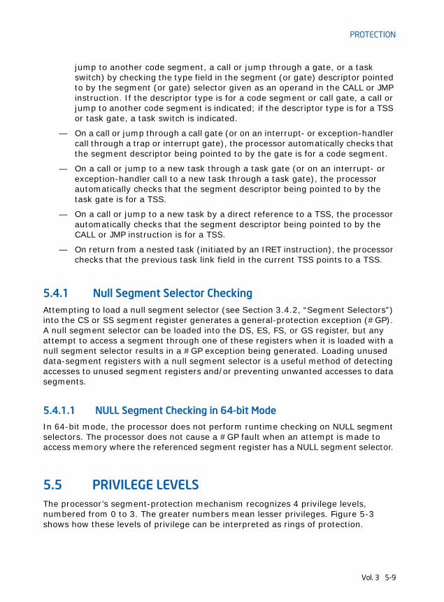
PROTECTION
jump to another code segment, a call or jump through a gate, or a task switch) by checking the type field in the segment (or gate) descriptor pointed to by the segment (or gate) selector given as an operand in the CALL or JMP instruction. If the descriptor type is for a code segment or call gate, a call or jump to another code segment is indicated; if the descriptor type is for a TSS or task gate, a task switch is indicated.
— On a call or jump through a call gate (or on an interrupt- or exception-handler call through a trap or interrupt gate), the processor automatically checks that the segment descriptor being pointed to by the gate is for a code segment.
— On a call or jump to a new task through a task gate (or on an interrupt- or exception-handler call to a new task through a task gate), the processor automatically checks that the segment descriptor being pointed to by the task gate is for a TSS.
— On a call or jump to a new task by a direct reference to a TSS, the processor automatically checks that the segment descriptor being pointed to by the CALL or JMP instruction is for a TSS.
— On return from a nested task (initiated by an IRET instruction), the processor checks that the previous task link field in the current TSS points to a TSS.
5.4.1 Null Segment Selector CheckingAttempting to load a null segment selector (see Section 3.4.2, “Segment Selectors”) into the CS or SS segment register generates a general-protection exception (#GP). A null segment selector can be loaded into the DS, ES, FS, or GS register, but any attempt to access a segment through one of these registers when it is loaded with a null segment selector results in a #GP exception being generated. Loading unused data-segment registers with a null segment selector is a useful method of detecting accesses to unused segment registers and/or preventing unwanted accesses to data segments.
5.4.1.1 NULL Segment Checking in 64-bit ModeIn 64-bit mode, the processor does not perform runtime checking on NULL segment selectors. The processor does not cause a #GP fault when an attempt is made to access memory where the referenced segment register has a NULL segment selector.
5.5 PRIVILEGE LEVELSThe processor’s segment-protection mechanism recognizes 4 privilege levels, numbered from 0 to 3. The greater numbers mean lesser privileges. Figure 5-3 shows how these levels of privilege can be interpreted as rings of protection.
Vol. 3 5-9
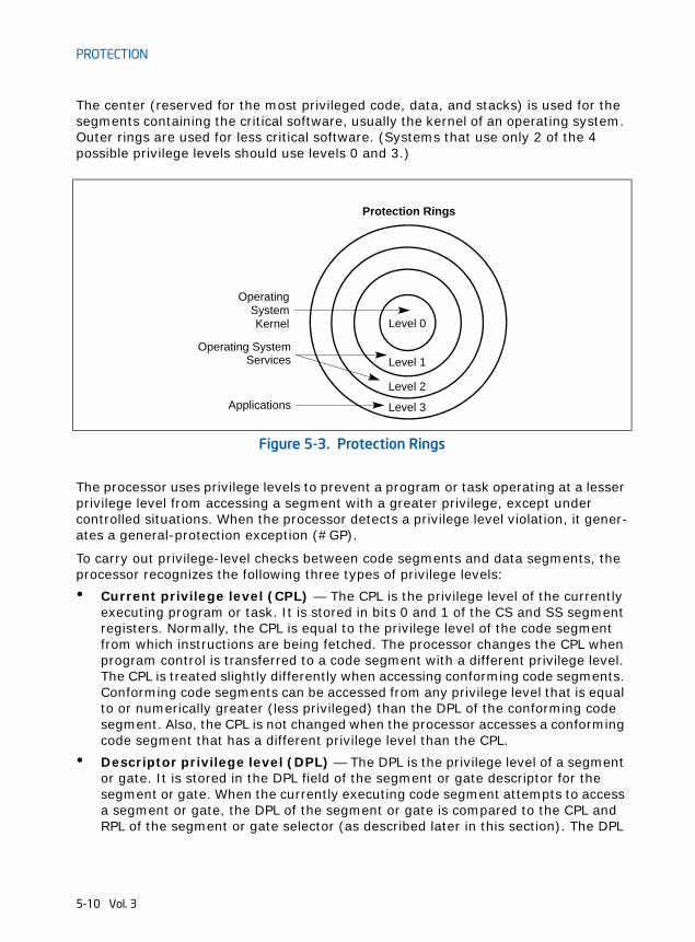
PROTECTION
The center (reserved for the most privileged code, data, and stacks) is used for the segments containing the critical software, usually the kernel of an operating system. Outer rings are used for less critical software. (Systems that use only 2 of the 4 possible privilege levels should use levels 0 and 3.)
The processor uses privilege levels to prevent a program or task operating at a lesser privilege level from accessing a segment with a greater privilege, except under controlled situations. When the processor detects a privilege level violation, it gener-ates a general-protection exception (#GP).
To carry out privilege-level checks between code segments and data segments, the processor recognizes the following three types of privilege levels:
• Current privilege level (CPL) — The CPL is the privilege level of the currently executing program or task. It is stored in bits 0 and 1 of the CS and SS segment registers. Normally, the CPL is equal to the privilege level of the code segment from which instructions are being fetched. The processor changes the CPL when program control is transferred to a code segment with a different privilege level. The CPL is treated slightly differently when accessing conforming code segments. Conforming code segments can be accessed from any privilege level that is equal to or numerically greater (less privileged) than the DPL of the conforming code segment. Also, the CPL is not changed when the processor accesses a conforming code segment that has a different privilege level than the CPL.
• Descriptor privilege level (DPL) — The DPL is the privilege level of a segment or gate. It is stored in the DPL field of the segment or gate descriptor for the segment or gate. When the currently executing code segment attempts to access a segment or gate, the DPL of the segment or gate is compared to the CPL and RPL of the segment or gate selector (as described later in this section). The DPL
Figure 5-3. Protection Rings
Level 0
Level 1
Level 2
Level 3
Protection Rings
Operating
Operating SystemServices
SystemKernel
Applications
5-10 Vol. 3

PROTECTION
is interpreted differently, depending on the type of segment or gate being accessed:
— Data segment — The DPL indicates the numerically highest privilege level that a program or task can have to be allowed to access the segment. For example, if the DPL of a data segment is 1, only programs running at a CPL of 0 or 1 can access the segment.
— Nonconforming code segment (without using a call gate) — The DPL indicates the privilege level that a program or task must be at to access the segment. For example, if the DPL of a nonconforming code segment is 0, only programs running at a CPL of 0 can access the segment.
— Call gate — The DPL indicates the numerically highest privilege level that the currently executing program or task can be at and still be able to access the call gate. (This is the same access rule as for a data segment.)
— Conforming code segment and nonconforming code segment accessed through a call gate — The DPL indicates the numerically lowest privilege level that a program or task can have to be allowed to access the segment. For example, if the DPL of a conforming code segment is 2, programs running at a CPL of 0 or 1 cannot access the segment.
— TSS — The DPL indicates the numerically highest privilege level that the currently executing program or task can be at and still be able to access the TSS. (This is the same access rule as for a data segment.)
• Requested privilege level (RPL) — The RPL is an override privilege level that is assigned to segment selectors. It is stored in bits 0 and 1 of the segment selector. The processor checks the RPL along with the CPL to determine if access to a segment is allowed. Even if the program or task requesting access to a segment has sufficient privilege to access the segment, access is denied if the RPL is not of sufficient privilege level. That is, if the RPL of a segment selector is numerically greater than the CPL, the RPL overrides the CPL, and vice versa. The RPL can be used to insure that privileged code does not access a segment on behalf of an application program unless the program itself has access privileges for that segment. See Section 5.10.4, “Checking Caller Access Privileges (ARPL Instruction),” for a detailed description of the purpose and typical use of the RPL.
Privilege levels are checked when the segment selector of a segment descriptor is loaded into a segment register. The checks used for data access differ from those used for transfers of program control among code segments; therefore, the two kinds of accesses are considered separately in the following sections.
5.6 PRIVILEGE LEVEL CHECKING WHEN ACCESSING DATA SEGMENTS
To access operands in a data segment, the segment selector for the data segment must be loaded into the data-segment registers (DS, ES, FS, or GS) or into the stack-
Vol. 3 5-11

PROTECTION
5.6.1 Accessing Data in Code SegmentsIn some instances it may be desirable to access data structures that are contained in a code segment. The following methods of accessing data in code segments are possible:
• Load a data-segment register with a segment selector for a nonconforming, readable, code segment.
• Load a data-segment register with a segment selector for a conforming, readable, code segment.
• Use a code-segment override prefix (CS) to read a readable, code segment whose selector is already loaded in the CS register.
The same rules for accessing data segments apply to method 1. Method 2 is always valid because the privilege level of a conforming code segment is effectively the same as the CPL, regardless of its DPL. Method 3 is always valid because the DPL of the code segment selected by the CS register is the same as the CPL.
5.7 PRIVILEGE LEVEL CHECKING WHEN LOADING THE SS REGISTER
Privilege level checking also occurs when the SS register is loaded with the segment selector for a stack segment. Here all privilege levels related to the stack segment must match the CPL; that is, the CPL, the RPL of the stack-segment selector, and the DPL of the stack-segment descriptor must be the same. If the RPL and DPL are not equal to the CPL, a general-protection exception (#GP) is generated.
5.8 PRIVILEGE LEVEL CHECKING WHEN TRANSFERRING PROGRAM CONTROL BETWEEN CODE SEGMENTS
To transfer program control from one code segment to another, the segment selector for the destination code segment must be loaded into the code-segment register (CS). As part of this loading process, the processor examines the segment descriptor for the destination code segment and performs various limit, type, and privilege checks. If these checks are successful, the CS register is loaded, program control is transferred to the new code segment, and program execution begins at the instruc-tion pointed to by the EIP register.
Program control transfers are carried out with the JMP, CALL, RET, SYSENTER, SYSEXIT, INT n, and IRET instructions, as well as by the exception and interrupt mechanisms. Exceptions, interrupts, and the IRET instruction are special cases discussed in Chapter 6, “Interrupt and Exception Handling.” This chapter discusses only the JMP, CALL, RET, SYSENTER, and SYSEXIT instructions.
A JMP or CALL instruction can reference another code segment in any of four ways:
5-14 Vol. 3

PROTECTION
• The target operand contains the segment selector for the target code segment.
• The target operand points to a call-gate descriptor, which contains the segment selector for the target code segment.
• The target operand points to a TSS, which contains the segment selector for the target code segment.
• The target operand points to a task gate, which points to a TSS, which in turn contains the segment selector for the target code segment.
The following sections describe first two types of references. See Section 7.3, “Task Switching,” for information on transferring program control through a task gate and/or TSS.
The SYSENTER and SYSEXIT instructions are special instructions for making fast calls to and returns from operating system or executive procedures. These instructions are discussed briefly in Section 5.8.7, “Performing Fast Calls to System Procedures with the SYSENTER and SYSEXIT Instructions.”
5.8.1 Direct Calls or Jumps to Code SegmentsThe near forms of the JMP, CALL, and RET instructions transfer program control within the current code segment, so privilege-level checks are not performed. The far forms of the JMP, CALL, and RET instructions transfer control to other code segments, so the processor does perform privilege-level checks.
When transferring program control to another code segment without going through a call gate, the processor examines four kinds of privilege level and type information (see Figure 5-6):
• The CPL. (Here, the CPL is the privilege level of the calling code segment; that is, the code segment that contains the procedure that is making the call or jump.)
Figure 5-6. Privilege Check for Control Transfer Without Using a Gate
CPL
RPL
DPL
PrivilegeCheck
CS Register
Segment SelectorFor Code Segment
Destination CodeSegment Descriptor
C
Vol. 3 5-15

PROTECTION
The RPL of the segment selector that points to a nonconforming code segment has a limited effect on the privilege check. The RPL must be numerically less than or equal to the CPL of the calling procedure for a successful control transfer to occur. So, in the example in Figure 5-7, the RPLs of segment selectors C1 and C2 could legally be set to 0, 1, or 2, but not to 3.
When the segment selector of a nonconforming code segment is loaded into the CS register, the privilege level field is not changed; that is, it remains at the CPL (which is the privilege level of the calling procedure). This is true, even if the RPL of the segment selector is different from the CPL.
5.8.1.2 Accessing Conforming Code SegmentsWhen accessing conforming code segments, the CPL of the calling procedure may be numerically equal to or greater than (less privileged) the DPL of the destination code segment; the processor generates a general-protection exception (#GP) only if the CPL is less than the DPL. (The segment selector RPL for the destination code segment is not checked if the segment is a conforming code segment.)
Figure 5-7. Examples of Accessing Conforming and Nonconforming Code Segments From Various Privilege Levels
CodeSegment D
CodeSegment CCode
Segment A
Lowest Privilege
Highest Privilege
CPL=3
CodeSegment B
NonconformingCode Segment
ConformingCode Segment
3
2
1
0
CPL=2DPL=2
DPL=1
Segment Sel. D1RPL=2
Segment Sel. D2RPL=3
Segment Sel. C2RPL=3
Segment Sel. C1RPL=2
Vol. 3 5-17
PROTECTION
In the example in Figure 5-7, code segment D is a conforming code segment. There-fore, calling procedures in both code segment A and B can access code segment D (using either segment selector D1 or D2, respectively), because they both have CPLs that are greater than or equal to the DPL of the conforming code segment. For conforming code segments, the DPL represents the numerically lowest priv-ilege level that a calling procedure may be at to successfully make a call to the code segment.
(Note that segments selectors D1 and D2 are identical except for their respective RPLs. But since RPLs are not checked when accessing conforming code segments, the two segment selectors are essentially interchangeable.)
When program control is transferred to a conforming code segment, the CPL does not change, even if the DPL of the destination code segment is less than the CPL. This situation is the only one where the CPL may be different from the DPL of the current code segment. Also, since the CPL does not change, no stack switch occurs.
Conforming segments are used for code modules such as math libraries and excep-tion handlers, which support applications but do not require access to protected system facilities. These modules are part of the operating system or executive soft-ware, but they can be executed at numerically higher privilege levels (less privileged levels). Keeping the CPL at the level of a calling code segment when switching to a conforming code segment prevents an application program from accessing noncon-forming code segments while at the privilege level (DPL) of a conforming code segment and thus prevents it from accessing more privileged data.
Most code segments are nonconforming. For these segments, program control can be transferred only to code segments at the same level of privilege, unless the transfer is carried out through a call gate, as described in the following sections.
5.8.2 Gate DescriptorsTo provide controlled access to code segments with different privilege levels, the processor provides special set of descriptors called gate descriptors. There are four kinds of gate descriptors:
• Call gates
• Trap gates
• Interrupt gates
• Task gates
Task gates are used for task switching and are discussed in Chapter 7, “Task Manage-ment”. Trap and interrupt gates are special kinds of call gates used for calling excep-tion and interrupt handlers. The are described in Chapter 6, “Interrupt and Exception Handling.” This chapter is concerned only with call gates.
5-18 Vol. 3

PROTECTION
5.8.3 Call GatesCall gates facilitate controlled transfers of program control between different privi-lege levels. They are typically used only in operating systems or executives that use the privilege-level protection mechanism. Call gates are also useful for transferring program control between 16-bit and 32-bit code segments, as described in Section 18.4, “Transferring Control Among Mixed-Size Code Segments.”
Figure 5-8 shows the format of a call-gate descriptor. A call-gate descriptor may reside in the GDT or in an LDT, but not in the interrupt descriptor table (IDT). It performs six functions:
• It specifies the code segment to be accessed.
• It defines an entry point for a procedure in the specified code segment.
• It specifies the privilege level required for a caller trying to access the procedure.
• If a stack switch occurs, it specifies the number of optional parameters to be copied between stacks.
• It defines the size of values to be pushed onto the target stack: 16-bit gates force 16-bit pushes and 32-bit gates force 32-bit pushes.
• It specifies whether the call-gate descriptor is valid.
The segment selector field in a call gate specifies the code segment to be accessed. The offset field specifies the entry point in the code segment. This entry point is generally to the first instruction of a specific procedure. The DPL field indicates the privilege level of the call gate, which in turn is the privilege level required to access the selected procedure through the gate. The P flag indicates whether the call-gate descriptor is valid. (The presence of the code segment to which the gate points is indicated by the P flag in the code segment’s descriptor.) The parameter count field indicates the number of parameters to copy from the calling procedures stack to the new stack if a stack switch occurs (see Section 5.8.5, “Stack Switching”). The param-eter count specifies the number of words for 16-bit call gates and doublewords for 32-bit call gates.
Figure 5-8. Call-Gate Descriptor
31 16 15 1314 12 11 8 7 0
POffset in Segment 31:16DPL
Type
04
31 16 15 0
Segment Selector Offset in Segment 15:00 0
Param.0011
PDPL
Gate ValidDescriptor Privilege Level
Count
456
0 0 0
Vol. 3 5-19

PROTECTION
Note that the P flag in a gate descriptor is normally always set to 1. If it is set to 0, a not present (#NP) exception is generated when a program attempts to access the descriptor. The operating system can use the P flag for special purposes. For example, it could be used to track the number of times the gate is used. Here, the P flag is initially set to 0 causing a trap to the not-present exception handler. The exception handler then increments a counter and sets the P flag to 1, so that on returning from the handler, the gate descriptor will be valid.
5.8.3.1 IA-32e Mode Call GatesCall-gate descriptors in 32-bit mode provide a 32-bit offset for the instruction pointer (EIP); 64-bit extensions double the size of 32-bit mode call gates in order to store 64-bit instruction pointers (RIP). See Figure 5-9:
• The first eight bytes (bytes 7:0) of a 64-bit mode call gate are similar but not identical to legacy 32-bit mode call gates. The parameter-copy-count field has been removed.
• Bytes 11:8 hold the upper 32 bits of the target-segment offset in canonical form. A general-protection exception (#GP) is generated if software attempts to use a call gate with a target offset that is not in canonical form.
• 16-byte descriptors may reside in the same descriptor table with 16-bit and 32-bit descriptors. A type field, used for consistency checking, is defined in bits 12:8 of the 64-bit descriptor’s highest dword (cleared to zero). A general-protection exception (#GP) results if an attempt is made to access the upper half of a 64-bit mode descriptor as a 32-bit mode descriptor.
5-20 Vol. 3

PROTECTION
5.8.4 Accessing a Code Segment Through a Call GateTo access a call gate, a far pointer to the gate is provided as a target operand in a CALL or JMP instruction. The segment selector from this pointer identifies the call gate (see Figure 5-10); the offset from the pointer is required, but not used or checked by the processor. (The offset can be set to any value.)
When the processor has accessed the call gate, it uses the segment selector from the call gate to locate the segment descriptor for the destination code segment. (This segment descriptor can be in the GDT or the LDT.) It then combines the base address from the code-segment descriptor with the offset from the call gate to form the linear address of the procedure entry point in the code segment.
As shown in Figure 5-11, four different privilege levels are used to check the validity of a program control transfer through a call gate:
• The CPL (current privilege level).
• The RPL (requestor's privilege level) of the call gate’s selector.
• The DPL (descriptor privilege level) of the call gate descriptor.
• The DPL of the segment descriptor of the destination code segment.
The C flag (conforming) in the segment descriptor for the destination code segment is also checked.
Figure 5-10. Call-Gate Mechanism
OffsetSegment Selector
Far Pointer to Call Gate
Required but not used by processor
Call-GateDescriptor
Code-SegmentDescriptor
Descriptor Table
Offset
BaseBase
Offset
Base
Segment Selector
+ProcedureEntry Point
5-22 Vol. 3

PROTECTION
The privilege checking rules are different depending on whether the control transfer was initiated with a CALL or a JMP instruction, as shown in Table 5-1.
The DPL field of the call-gate descriptor specifies the numerically highest privilege level from which a calling procedure can access the call gate; that is, to access a call gate, the CPL of a calling procedure must be equal to or less than the DPL of the call gate. For example, in Figure 5-15, call gate A has a DPL of 3. So calling procedures at all CPLs (0 through 3) can access this call gate, which includes calling procedures in code segments A, B, and C. Call gate B has a DPL of 2, so only calling procedures at a CPL or 0, 1, or 2 can access call gate B, which includes calling procedures in code
Figure 5-11. Privilege Check for Control Transfer with Call Gate
Table 5-1. Privilege Check Rules for Call Gates
Instruction Privilege Check Rules
CALL CPL ≤ call gate DPL; RPL ≤ call gate DPL
Destination conforming code segment DPL ≤ CPL
Destination nonconforming code segment DPL ≤ CPL
JMP CPL ≤ call gate DPL; RPL ≤ call gate DPL
Destination conforming code segment DPL ≤ CPL
Destination nonconforming code segment DPL = CPL
CPL
RPL
DPL
DPL
PrivilegeCheck
Call Gate (Descriptor)
Destination Code-
CS Register
Call-Gate Selector
Segment Descriptor
Vol. 3 5-23

PROTECTION
segments B and C. The dotted line shows that a calling procedure in code segment A cannot access call gate B.
The RPL of the segment selector to a call gate must satisfy the same test as the CPL of the calling procedure; that is, the RPL must be less than or equal to the DPL of the call gate. In the example in Figure 5-15, a calling procedure in code segment C can access call gate B using gate selector B2 or B1, but it could not use gate selector B3 to access call gate B.
If the privilege checks between the calling procedure and call gate are successful, the processor then checks the DPL of the code-segment descriptor against the CPL of the calling procedure. Here, the privilege check rules vary between CALL and JMP instructions. Only CALL instructions can use call gates to transfer program control to more privileged (numerically lower privilege level) nonconforming code segments; that is, to nonconforming code segments with a DPL less than the CPL. A JMP instruc-tion can use a call gate only to transfer program control to a nonconforming code segment with a DPL equal to the CPL. CALL and JMP instruction can both transfer program control to a more privileged conforming code segment; that is, to a conforming code segment with a DPL less than or equal to the CPL.
If a call is made to a more privileged (numerically lower privilege level) noncon-forming destination code segment, the CPL is lowered to the DPL of the destination code segment and a stack switch occurs (see Section 5.8.5, “Stack Switching”). If a call or jump is made to a more privileged conforming destination code segment, the CPL is not changed and no stack switch occurs.
5-24 Vol. 3
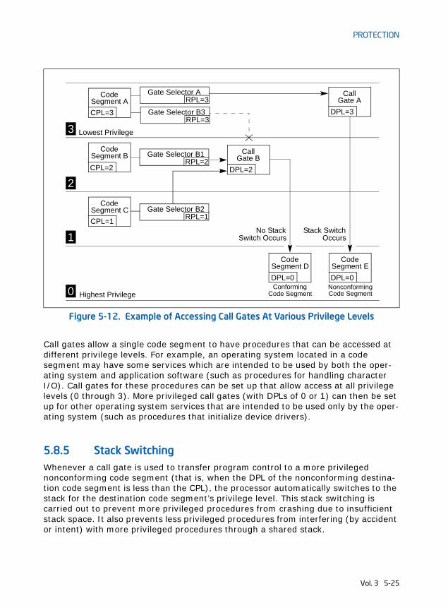
PROTECTION
Call gates allow a single code segment to have procedures that can be accessed at different privilege levels. For example, an operating system located in a code segment may have some services which are intended to be used by both the oper-ating system and application software (such as procedures for handling character I/O). Call gates for these procedures can be set up that allow access at all privilege levels (0 through 3). More privileged call gates (with DPLs of 0 or 1) can then be set up for other operating system services that are intended to be used only by the oper-ating system (such as procedures that initialize device drivers).
5.8.5 Stack SwitchingWhenever a call gate is used to transfer program control to a more privileged nonconforming code segment (that is, when the DPL of the nonconforming destina-tion code segment is less than the CPL), the processor automatically switches to the stack for the destination code segment’s privilege level. This stack switching is carried out to prevent more privileged procedures from crashing due to insufficient stack space. It also prevents less privileged procedures from interfering (by accident or intent) with more privileged procedures through a shared stack.
Figure 5-12. Example of Accessing Call Gates At Various Privilege Levels
CodeSegment A
Stack SwitchNo StackSwitch Occurs Occurs
Lowest Privilege
Highest Privilege
3
2
1
0
CallGate A
CodeSegment B Call
Gate B
CodeSegment C
CodeSegment D
CodeSegment E
NonconformingCode Segment
ConformingCode Segment
Gate Selector ARPL=3
Gate Selector B1RPL=2
Gate Selector B2RPL=1
CPL=3
CPL=2
CPL=1
DPL=3
DPL=2
DPL=0 DPL=0
Gate Selector B3RPL=3
Vol. 3 5-25

PROTECTION
Each task must define up to 4 stacks: one for applications code (running at privilege level 3) and one for each of the privilege levels 2, 1, and 0 that are used. (If only two privilege levels are used [3 and 0], then only two stacks must be defined.) Each of these stacks is located in a separate segment and is identified with a segment selector and an offset into the stack segment (a stack pointer).
The segment selector and stack pointer for the privilege level 3 stack is located in the SS and ESP registers, respectively, when privilege-level-3 code is being executed and is automatically stored on the called procedure’s stack when a stack switch occurs.
Pointers to the privilege level 0, 1, and 2 stacks are stored in the TSS for the currently running task (see Figure 7-2). Each of these pointers consists of a segment selector and a stack pointer (loaded into the ESP register). These initial pointers are strictly read-only values. The processor does not change them while the task is running. They are used only to create new stacks when calls are made to more privileged levels (numerically lower privilege levels). These stacks are disposed of when a return is made from the called procedure. The next time the procedure is called, a new stack is created using the initial stack pointer. (The TSS does not specify a stack for privilege level 3 because the processor does not allow a transfer of program control from a procedure running at a CPL of 0, 1, or 2 to a procedure running at a CPL of 3, except on a return.)
The operating system is responsible for creating stacks and stack-segment descrip-tors for all the privilege levels to be used and for loading initial pointers for these stacks into the TSS. Each stack must be read/write accessible (as specified in the type field of its segment descriptor) and must contain enough space (as specified in the limit field) to hold the following items:
• The contents of the SS, ESP, CS, and EIP registers for the calling procedure.
• The parameters and temporary variables required by the called procedure.
• The EFLAGS register and error code, when implicit calls are made to an exception or interrupt handler.
The stack will need to require enough space to contain many frames of these items, because procedures often call other procedures, and an operating system may support nesting of multiple interrupts. Each stack should be large enough to allow for the worst case nesting scenario at its privilege level.
(If the operating system does not use the processor’s multitasking mechanism, it still must create at least one TSS for this stack-related purpose.)
When a procedure call through a call gate results in a change in privilege level, the processor performs the following steps to switch stacks and begin execution of the called procedure at a new privilege level:
1. Uses the DPL of the destination code segment (the new CPL) to select a pointerto the new stack (segment selector and stack pointer) from the TSS.
2. Reads the segment selector and stack pointer for the stack to be switched to from the current TSS. Any limit violations detected while reading the stack-segment selector, stack pointer, or stack-segment descriptor cause an invalid TSS (#TS) exception to be generated.
5-26 Vol. 3

PROTECTION
3. Checks the stack-segment descriptor for the proper privileges and type and generates an invalid TSS (#TS) exception if violations are detected.
4. Temporarily saves the current values of the SS and ESP registers.
5. Loads the segment selector and stack pointer for the new stack in the SS and ESP registers.
6. Pushes the temporarily saved values for the SS and ESP registers (for the calling procedure) onto the new stack (see Figure 5-13).
7. Copies the number of parameter specified in the parameter count field of the call gate from the calling procedure’s stack to the new stack. If the count is 0, no parameters are copied.
8. Pushes the return instruction pointer (the current contents of the CS and EIP registers) onto the new stack.
9. Loads the segment selector for the new code segment and the new instruction pointer from the call gate into the CS and EIP registers, respectively, and begins execution of the called procedure.
See the description of the CALL instruction in Chapter 3, Instruction Set Reference, in the IA-32 Intel Architecture Software Developer’s Manual, Volume 2, for a detailed description of the privilege level checks and other protection checks that the processor performs on a far call through a call gate.
The parameter count field in a call gate specifies the number of data items (up to 31) that the processor should copy from the calling procedure’s stack to the stack of the called procedure. If more than 31 data items need to be passed to the called proce-
Figure 5-13. Stack Switching During an Interprivilege-Level Call
Parameter 1
Parameter 2
Parameter 3
Calling SS
Calling ESP
Parameter 1
Parameter 2
Parameter 3
Calling CS
Calling EIP
Called Procedure’s Stack
ESP
ESP
Calling Procedure’s Stack
Vol. 3 5-27

PROTECTION
dure, one of the parameters can be a pointer to a data structure, or the saved contents of the SS and ESP registers may be used to access parameters in the old stack space. The size of the data items passed to the called procedure depends on the call gate size, as described in Section 5.8.3, “Call Gates.”
5.8.5.1 Stack Switching in 64-bit ModeAlthough protection-check rules for call gates are unchanged from 32-bit mode, stack-switch changes in 64-bit mode are different.
When stacks are switched as part of a 64-bit mode privilege-level change through a call gate, a new SS (stack segment) descriptor is not loaded; 64-bit mode only loads an inner-level RSP from the TSS. The new SS is forced to NULL and the SS selector’s RPL field is forced to the new CPL. The new SS is set to NULL in order to handle nested far transfers (CALLF, INTn, interrupts and exceptions). The old SS and RSP are saved on the new stack.
On a subsequent RETF, the old SS is popped from the stack and loaded into the SS register. See Table 5-2.
In 64-bit mode, stack operations resulting from a privilege-level-changing far call or far return are eight-bytes wide and change the RSP by eight. The mode does not support the automatic parameter-copy feature found in 32-bit mode. The call-gate count field is ignored. Software can access the old stack, if necessary, by referencing the old stack-segment selector and stack pointer saved on the new process stack.
In 64-bit mode, RETF is allowed to load a NULL SS under certain conditions. If the target mode is 64-bit mode and the target CPL< >3, IRET allows SS to be loaded with a NULL selector. If the called procedure itself is interrupted, the NULL SS is pushed on the stack frame. On the subsequent RETF, the NULL SS on the stack acts as a flag to tell the processor not to load a new SS descriptor.
5.8.6 Returning from a Called ProcedureThe RET instruction can be used to perform a near return, a far return at the same privilege level, and a far return to a different privilege level. This instruction is
Table 5-2. 64-Bit-Mode Stack Layout After CALLF with CPL Change32-bit Mode IA-32e mode
Old SS Selector +12 +24 Old SS Selector
Old ESP +8 +16 Old RSP
CS Selector +4 +8 Old CS Selector
EIP 0 ESP RSP 0 RIP
< 4 Bytes > < 8 Bytes >
5-28 Vol. 3
PROTECTION
intended to execute returns from procedures that were called with a CALL instruc-tion. It does not support returns from a JMP instruction, because the JMP instruction does not save a return instruction pointer on the stack.
A near return only transfers program control within the current code segment; there-fore, the processor performs only a limit check. When the processor pops the return instruction pointer from the stack into the EIP register, it checks that the pointer does not exceed the limit of the current code segment.
On a far return at the same privilege level, the processor pops both a segment selector for the code segment being returned to and a return instruction pointer from the stack. Under normal conditions, these pointers should be valid, because they were pushed on the stack by the CALL instruction. However, the processor performs privilege checks to detect situations where the current procedure might have altered the pointer or failed to maintain the stack properly.
A far return that requires a privilege-level change is only allowed when returning to a less privileged level (that is, the DPL of the return code segment is numerically greater than the CPL). The processor uses the RPL field from the CS register value saved for the calling procedure (see Figure 5-13) to determine if a return to a numer-ically higher privilege level is required. If the RPL is numerically greater (less privi-leged) than the CPL, a return across privilege levels occurs.
The processor performs the following steps when performing a far return to a calling procedure (see Figures 6-2 and 6-4 in the Intel® 64 and IA-32 Architectures Soft-ware Developer’s Manual, Volume 1, for an illustration of the stack contents prior to and after a return):
1. Checks the RPL field of the saved CS register value to determine if a privilegelevel change is required on the return.
2. Loads the CS and EIP registers with the values on the called procedure’s stack. (Type and privilege level checks are performed on the code-segment descriptor and RPL of the code- segment selector.)
3. (If the RET instruction includes a parameter count operand and the return requires a privilege level change.) Adds the parameter count (in bytes obtained from the RET instruction) to the current ESP register value (after popping the CS and EIP values), to step past the parameters on the called procedure’s stack. The resulting value in the ESP register points to the saved SS and ESP values for the calling procedure’s stack. (Note that the byte count in the RET instruction must be chosen to match the parameter count in the call gate that the calling procedure referenced when it made the original call multiplied by the size of the parameters.)
4. (If the return requires a privilege level change.) Loads the SS and ESP registers with the saved SS and ESP values and switches back to the calling procedure’s stack. The SS and ESP values for the called procedure’s stack are discarded. Any limit violations detected while loading the stack-segment selector or stack pointer cause a general-protection exception (#GP) to be generated. The new stack-segment descriptor is also checked for type and privilege violations.
Vol. 3 5-29

PROTECTION
5. (If the RET instruction includes a parameter count operand.) Adds the parameter count (in bytes obtained from the RET instruction) to the current ESP register value, to step past the parameters on the calling procedure’s stack. The resulting ESP value is not checked against the limit of the stack segment. If the ESP value is beyond the limit, that fact is not recognized until the next stack operation.
6. (If the return requires a privilege level change.) Checks the contents of the DS, ES, FS, and GS segment registers. If any of these registers refer to segments whose DPL is less than the new CPL (excluding conforming code segments), the segment register is loaded with a null segment selector.
See the description of the RET instruction in Chapter 4 of the Intel® 64 and IA-32 Architectures Software Developer’s Manual, Volume 2B, for a detailed description of the privilege level checks and other protection checks that the processor performs on a far return.
5.8.7 Performing Fast Calls to System Procedures with theSYSENTER and SYSEXIT Instructions
The SYSENTER and SYSEXIT instructions were introduced into the IA-32 architecture in the Pentium II processors for the purpose of providing a fast (low overhead) mech-anism for calling operating system or executive procedures. SYSENTER is intended for use by user code running at privilege level 3 to access operating system or exec-utive procedures running at privilege level 0. SYSEXIT is intended for use by privilege level 0 operating system or executive procedures for fast returns to privilege level 3 user code. SYSENTER can be executed from privilege levels 3, 2, 1, or 0; SYSEXIT can only be executed from privilege level 0.
The SYSENTER and SYSEXIT instructions are companion instructions, but they do not constitute a call/return pair. This is because SYSENTER does not save any state infor-mation for use by SYSEXIT on a return.
The target instruction and stack pointer for these instructions are not specified through instruction operands. Instead, they are specified through parameters entered in MSRs and general-purpose registers.
For SYSENTER, target fields are generated using the following sources:
• Target code segment — Reads this from IA32_SYSENTER_CS.
• Target instruction — Reads this from IA32_SYSENTER_EIP.
• Stack segment — Computed by adding 8 to the value in IA32_SYSENTER_CS.
• Stack pointer — Reads this from the IA32_SYSENTER_ESP.
For SYSEXIT, target fields are generated using the following sources:
• Target code segment — Computed by adding 16 to the value in the IA32_SYSENTER_CS.
• Target instruction — Reads this from EDX.
5-30 Vol. 3

PROTECTION
When SYSRET transfers control to 32-bit mode user code using a 32-bit operand size, the processor gets the privilege level 3 target instruction and stack pointer from:
• Target code segment — Reads a non-NULL selector from IA32_STAR[63:48].
• Target instruction — Copies the value in ECX into EIP.
• Stack segment — IA32_STAR[63:48] + 8.
• EFLAGS — Loaded from R11.
It is the responsibility of the OS to ensure the descriptors in the GDT/LDT correspond to the selectors loaded by SYSCALL/SYSRET (consistent with the base, limit, and attribute values forced by the instructions).
Any address written to IA32_LSTAR is first checked by WRMSR to ensure canonical form. If an address is not canonical, an exception is generated (#GP).
See Figure 5-14 for the layout of IA32_STAR, IA32_LSTAR and IA32_FMASK.
5.9 PRIVILEGED INSTRUCTIONSSome of the system instructions (called “privileged instructions”) are protected from use by application programs. The privileged instructions control system functions (such as the loading of system registers). They can be executed only when the CPL is 0 (most privileged). If one of these instructions is executed when the CPL is not 0, a
Figure 5-14. MSRs Used by SYSCALL and SYSRET
63 32 31 0
63 0
63 0
Target RIP for 64-bit Mode Calling Program
SYSRET CS and SS SYSCALL CS and SS
48 47
IA32_STAR
IA32_LSTAR
IA32_FMASK
32 31
SYSCALL EFLAGS MaskReserved
Reserved
Vol. 3 5-33

PROTECTION
general-protection exception (#GP) is generated. The following system instructions are privileged instructions:
• LGDT — Load GDT register.
• LLDT — Load LDT register.
• LTR — Load task register.
• LIDT — Load IDT register.
• MOV (control registers) — Load and store control registers.
• LMSW — Load machine status word.
• CLTS — Clear task-switched flag in register CR0.
• MOV (debug registers) — Load and store debug registers.
• INVD — Invalidate cache, without writeback.
• WBINVD — Invalidate cache, with writeback.
• INVLPG —Invalidate TLB entry.
• HLT— Halt processor.
• RDMSR — Read Model-Specific Registers.
• WRMSR —Write Model-Specific Registers.
• RDPMC — Read Performance-Monitoring Counter.
• RDTSC — Read Time-Stamp Counter.
Some of the privileged instructions are available only in the more recent families of Intel 64 and IA-32 processors (see Section 19.13, “New Instructions In the Pentium and Later IA-32 Processors”).
The PCE and TSD flags in register CR4 (bits 4 and 2, respectively) enable the RDPMC and RDTSC instructions, respectively, to be executed at any CPL.
5.10 POINTER VALIDATIONWhen operating in protected mode, the processor validates all pointers to enforce protection between segments and maintain isolation between privilege levels. Pointer validation consists of the following checks:
1. Checking access rights to determine if the segment type is compatible with itsuse.
2. Checking read/write rights.
3. Checking if the pointer offset exceeds the segment limit.
4. Checking if the supplier of the pointer is allowed to access the segment.
5. Checking the offset alignment.
5-34 Vol. 3

PROTECTION
The example in Figure 5-15 demonstrates how the ARPL instruction is intended to be used. When the operating-system receives segment selector D2 from the application program, it uses the ARPL instruction to compare the RPL of the segment selector with the privilege level of the application program (represented by the code-segment selector pushed onto the stack). If the RPL is less than application program’s privi-lege level, the ARPL instruction changes the RPL of the segment selector to match the privilege level of the application program (segment selector D1). Using this instruc-tion thus prevents a procedure running at a numerically higher privilege level from accessing numerically lower privilege-level (more privileged) segments by lowering the RPL of a segment selector.
Note that the privilege level of the application program can be determined by reading the RPL field of the segment selector for the application-program’s code segment. This segment selector is stored on the stack as part of the call to the operating system. The operating system can copy the segment selector from the stack into a register for use as an operand for the ARPL instruction.
5.10.5 Checking AlignmentWhen the CPL is 3, alignment of memory references can be checked by setting the AM flag in the CR0 register and the AC flag in the EFLAGS register. Unaligned memory references generate alignment exceptions (#AC). The processor does not generate alignment exceptions when operating at privilege level 0, 1, or 2. See Table 6-7 for a description of the alignment requirements when alignment checking is enabled.
5.11 PAGE-LEVEL PROTECTIONPage-level protection can be used alone or applied to segments. When page-level protection is used with the flat memory model, it allows supervisor code and data (the operating system or executive) to be protected from user code and data (appli-cation programs). It also allows pages containing code to be write protected. When the segment- and page-level protection are combined, page-level read/write protec-tion allows more protection granularity within segments.
With page-level protection (as with segment-level protection) each memory refer-ence is checked to verify that protection checks are satisfied. All checks are made before the memory cycle is started, and any violation prevents the cycle from starting and results in a page-fault exception being generated. Because checks are performed in parallel with address translation, there is no performance penalty.
The processor performs two page-level protection checks:
• Restriction of addressable domain (supervisor and user modes).
• Page type (read only or read/write).
Violations of either of these checks results in a page-fault exception being generated. See Chapter 6, “Interrupt 14—Page-Fault Exception (#PF),” for an explanation of the
Vol. 3 5-39

PROTECTION
page-fault exception mechanism. This chapter describes the protection violations which lead to page-fault exceptions.
5.11.1 Page-Protection FlagsProtection information for pages is contained in two flags in a paging-structure entry (see Chapter 4): the read/write flag (bit 1) and the user/supervisor flag (bit 2). The protection checks use the flags in all paging structures.
5.11.2 Restricting Addressable DomainThe page-level protection mechanism allows restricting access to pages based on two privilege levels:
• Supervisor mode (U/S flag is 0)—(Most privileged) For the operating system or executive, other system software (such as device drivers), and protected system data (such as page tables).
• User mode (U/S flag is 1)—(Least privileged) For application code and data.
The segment privilege levels map to the page privilege levels as follows. If the processor is currently operating at a CPL of 0, 1, or 2, it is in supervisor mode; if it is operating at a CPL of 3, it is in user mode. When the processor is in supervisor mode, it can access all pages; when in user mode, it can access only user-level pages. (Note that the WP flag in control register CR0 modifies the supervisor permissions, as described in Section 5.11.3, “Page Type.”)
Note that to use the page-level protection mechanism, code and data segments must be set up for at least two segment-based privilege levels: level 0 for supervisor code and data segments and level 3 for user code and data segments. (In this model, the stacks are placed in the data segments.) To minimize the use of segments, a flat memory model can be used (see Section 3.2.1, “Basic Flat Model”).
Here, the user and supervisor code and data segments all begin at address zero in the linear address space and overlay each other. With this arrangement, operating-system code (running at the supervisor level) and application code (running at the user level) can execute as if there are no segments. Protection between operating-system and application code and data is provided by the processor’s page-level protection mechanism.
5.11.3 Page TypeThe page-level protection mechanism recognizes two page types:
• Read-only access (R/W flag is 0).
• Read/write access (R/W flag is 1).
5-40 Vol. 3
PROTECTION
When the processor is in supervisor mode and the WP flag in register CR0 is clear (its state following reset initialization), all pages are both readable and writable (write-protection is ignored). When the processor is in user mode, it can write only to user-mode pages that are read/write accessible. User-mode pages which are read/write or read-only are readable; supervisor-mode pages are neither readable nor writable from user mode. A page-fault exception is generated on any attempt to violate the protection rules.
Starting with the P6 family, Intel processors allow user-mode pages to be write-protected against supervisor-mode access. Setting CR0.WP = 1 enables supervisor-mode sensitivity to write protected pages. If CR0.WP = 1, read-only pages are not writable from any privilege level. This supervisor write-protect feature is useful for implementing a “copy-on-write” strategy used by some operating systems, such as UNIX*, for task creation (also called forking or spawning). When a new task is created, it is possible to copy the entire address space of the parent task. This gives the child task a complete, duplicate set of the parent's segments and pages. An alter-native copy-on-write strategy saves memory space and time by mapping the child's segments and pages to the same segments and pages used by the parent task. A private copy of a page gets created only when one of the tasks writes to the page. By using the WP flag and marking the shared pages as read-only, the supervisor can detect an attempt to write to a page, and can copy the page at that time.
5.11.4 Combining Protection of Both Levels of Page TablesFor any one page, the protection attributes of its page-directory entry (first-level page table) may differ from those of its page-table entry (second-level page table). The processor checks the protection for a page in both its page-directory and the page-table entries. Table 5-3 shows the protection provided by the possible combina-tions of protection attributes when the WP flag is clear.
5.11.5 Overrides to Page ProtectionThe following types of memory accesses are checked as if they are privilege-level 0 accesses, regardless of the CPL at which the processor is currently operating:
• Access to segment descriptors in the GDT, LDT, or IDT.
• Access to an inner-privilege-level stack during an inter-privilege-level call or a call to in exception or interrupt handler, when a change of privilege level occurs.
5.12 COMBINING PAGE AND SEGMENT PROTECTIONWhen paging is enabled, the processor evaluates segment protection first, then evaluates page protection. If the processor detects a protection violation at either the segment level or the page level, the memory access is not carried out and an
Vol. 3 5-41

PROTECTION
exception is generated. If an exception is generated by segmentation, no paging exception is generated.
Page-level protections cannot be used to override segment-level protection. For example, a code segment is by definition not writable. If a code segment is paged, setting the R/W flag for the pages to read-write does not make the pages writable. Attempts to write into the pages will be blocked by segment-level protection checks.
Page-level protection can be used to enhance segment-level protection. For example, if a large read-write data segment is paged, the page-protection mecha-nism can be used to write-protect individual pages.
Table 5-3. Combined Page-Directory and Page-Table Protection
Page-Directory Entry Page-Table Entry Combined Effect
Privilege Access Type Privilege Access Type Privilege Access Type
User Read-Only User Read-Only User Read-Only
User Read-Only User Read-Write User Read-Only
User Read-Write User Read-Only User Read-Only
User Read-Write User Read-Write User Read/Write
User Read-Only Supervisor Read-Only Supervisor Read/Write*
User Read-Only Supervisor Read-Write Supervisor Read/Write*
User Read-Write Supervisor Read-Only Supervisor Read/Write*
User Read-Write Supervisor Read-Write Supervisor Read/Write
Supervisor Read-Only User Read-Only Supervisor Read/Write*
Supervisor Read-Only User Read-Write Supervisor Read/Write*
Supervisor Read-Write User Read-Only Supervisor Read/Write*
Supervisor Read-Write User Read-Write Supervisor Read/Write
Supervisor Read-Only Supervisor Read-Only Supervisor Read/Write*
Supervisor Read-Only Supervisor Read-Write Supervisor Read/Write*
Supervisor Read-Write Supervisor Read-Only Supervisor Read/Write*
Supervisor Read-Write Supervisor Read-Write Supervisor Read/Write
NOTE:* If CR0.WP = 1, access type is determined by the R/W flags of the page-directory and page-table
entries. IF CR0.WP = 0, supervisor privilege permits read-write access.
5-42 Vol. 3

CHAPTER 6INTERRUPT AND EXCEPTION HANDLING
This chapter describes the interrupt and exception-handling mechanism when oper-ating in protected mode on an Intel 64 or IA-32 processor. Most of the information provided here also applies to interrupt and exception mechanisms used in real-address, virtual-8086 mode, and 64-bit mode.
Chapter 17, “8086 Emulation,” describes information specific to interrupt and excep-tion mechanisms in real-address and virtual-8086 mode. Section 6.14, “Exception and Interrupt Handling in 64-bit Mode,” describes information specific to interrupt and exception mechanisms in IA-32e mode and 64-bit sub-mode.
6.1 INTERRUPT AND EXCEPTION OVERVIEWInterrupts and exceptions are events that indicate that a condition exists somewhere in the system, the processor, or within the currently executing program or task that requires the attention of a processor. They typically result in a forced transfer of execution from the currently running program or task to a special software routine or task called an interrupt handler or an exception handler. The action taken by a processor in response to an interrupt or exception is referred to as servicing or handling the interrupt or exception.
Interrupts occur at random times during the execution of a program, in response to signals from hardware. System hardware uses interrupts to handle events external to the processor, such as requests to service peripheral devices. Software can also generate interrupts by executing the INT n instruction.
Exceptions occur when the processor detects an error condition while executing an instruction, such as division by zero. The processor detects a variety of error condi-tions including protection violations, page faults, and internal machine faults. The machine-check architecture of the Pentium 4, Intel Xeon, P6 family, and Pentium processors also permits a machine-check exception to be generated when internal hardware errors and bus errors are detected.
When an interrupt is received or an exception is detected, the currently running procedure or task is suspended while the processor executes an interrupt or excep-tion handler. When execution of the handler is complete, the processor resumes execution of the interrupted procedure or task. The resumption of the interrupted procedure or task happens without loss of program continuity, unless recovery from an exception was not possible or an interrupt caused the currently running program to be terminated.
This chapter describes the processor’s interrupt and exception-handling mechanism, when operating in protected mode. A description of the exceptions and the conditions that cause them to be generated is given at the end of this chapter.
Vol. 3 6-1

INTERRUPT AND EXCEPTION HANDLING
6.2 EXCEPTION AND INTERRUPT VECTORSTo aid in handling exceptions and interrupts, each architecturally defined exception and each interrupt condition requiring special handling by the processor is assigned a unique identification number, called a vector number. The processor uses the vector number assigned to an exception or interrupt as an index into the interrupt descriptor table (IDT). The table provides the entry point to an exception or interrupt handler (see Section 6.10, “Interrupt Descriptor Table (IDT)”).
The allowable range for vector numbers is 0 to 255. Vector numbers in the range 0 through 31 are reserved by the Intel 64 and IA-32 architectures for architecture-defined exceptions and interrupts. Not all of the vector numbers in this range have a currently defined function. The unassigned vector numbers in this range are reserved. Do not use the reserved vector numbers.
Vector numbers in the range 32 to 255 are designated as user-defined interrupts and are not reserved by the Intel 64 and IA-32 architecture. These interrupts are gener-ally assigned to external I/O devices to enable those devices to send interrupts to the processor through one of the external hardware interrupt mechanisms (see Section 6.3, “Sources of Interrupts”).
Table 6-1 shows vector number assignments for architecturally defined exceptions and for the NMI interrupt. This table gives the exception type (see Section 6.5, “Exception Classifications”) and indicates whether an error code is saved on the stack for the exception. The source of each predefined exception and the NMI interrupt is also given.
6.3 SOURCES OF INTERRUPTSThe processor receives interrupts from two sources:
• External (hardware generated) interrupts.
• Software-generated interrupts.
6.3.1 External InterruptsExternal interrupts are received through pins on the processor or through the local APIC. The primary interrupt pins on Pentium 4, Intel Xeon, P6 family, and Pentium processors are the LINT[1:0] pins, which are connected to the local APIC (see Chapter 10, “Advanced Programmable Interrupt Controller (APIC)”). When the local APIC is enabled, the LINT[1:0] pins can be programmed through the APIC’s local vector table (LVT) to be associated with any of the processor’s exception or interrupt vectors.
When the local APIC is global/hardware disabled, these pins are configured as INTR and NMI pins, respectively. Asserting the INTR pin signals the processor that an external interrupt has occurred. The processor reads from the system bus the inter-
6-2 Vol. 3

INTERRUPT AND EXCEPTION HANDLING
rupt vector number provided by an external interrupt controller, such as an 8259A (see Section 6.2, “Exception and Interrupt Vectors”). Asserting the NMI pin signals a non-maskable interrupt (NMI), which is assigned to interrupt vector 2.
Table 6-1. Protected-Mode Exceptions and Interrupts
Vector No.
Mne-monic
Description Type Error Code
Source
0 #DE Divide Error Fault No DIV and IDIV instructions.
1 #DB RESERVED Fault/ Trap
No For Intel use only.
2 — NMI Interrupt Interrupt No Nonmaskable external interrupt.
3 #BP Breakpoint Trap No INT 3 instruction.
4 #OF Overflow Trap No INTO instruction.
5 #BR BOUND Range Exceeded Fault No BOUND instruction.
6 #UD Invalid Opcode (Undefined Opcode)
Fault No UD2 instruction or reserved opcode.1
7 #NM Device Not Available (No Math Coprocessor)
Fault No Floating-point or WAIT/FWAIT instruction.
8 #DF Double Fault Abort Yes (zero)
Any instruction that can generate an exception, an NMI, or an INTR.
9 Coprocessor Segment Overrun (reserved)
Fault No Floating-point instruction.2
10 #TS Invalid TSS Fault Yes Task switch or TSS access.
11 #NP Segment Not Present Fault Yes Loading segment registers or accessing system segments.
12 #SS Stack-Segment Fault Fault Yes Stack operations and SS register loads.
13 #GP General Protection Fault Yes Any memory reference and other protection checks.
14 #PF Page Fault Fault Yes Any memory reference.
15 — (Intel reserved. Do not use.)
No
16 #MF x87 FPU Floating-Point Error (Math Fault)
Fault No x87 FPU floating-point or WAIT/FWAIT instruction.
17 #AC Alignment Check Fault Yes (Zero)
Any data reference in memory.3
Vol. 3 6-3
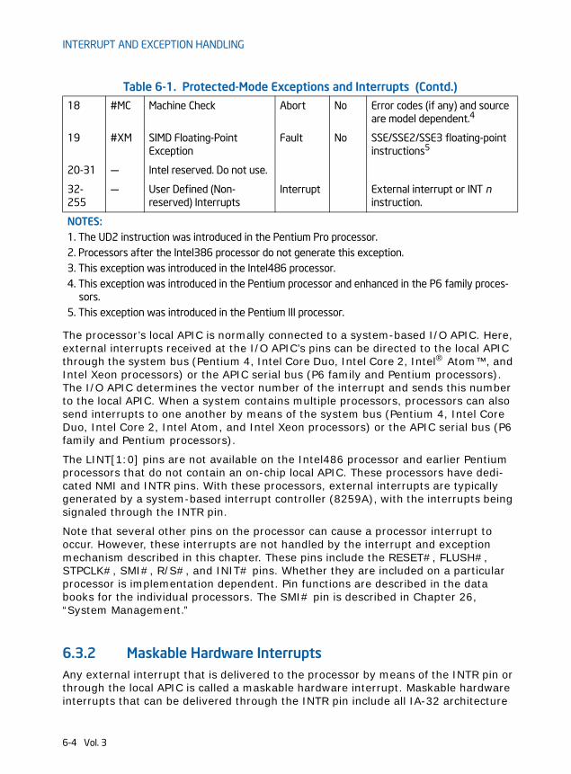
INTERRUPT AND EXCEPTION HANDLING
The processor’s local APIC is normally connected to a system-based I/O APIC. Here, external interrupts received at the I/O APIC’s pins can be directed to the local APIC through the system bus (Pentium 4, Intel Core Duo, Intel Core 2, Intel® Atom™, and Intel Xeon processors) or the APIC serial bus (P6 family and Pentium processors). The I/O APIC determines the vector number of the interrupt and sends this number to the local APIC. When a system contains multiple processors, processors can also send interrupts to one another by means of the system bus (Pentium 4, Intel Core Duo, Intel Core 2, Intel Atom, and Intel Xeon processors) or the APIC serial bus (P6 family and Pentium processors).
The LINT[1:0] pins are not available on the Intel486 processor and earlier Pentium processors that do not contain an on-chip local APIC. These processors have dedi-cated NMI and INTR pins. With these processors, external interrupts are typically generated by a system-based interrupt controller (8259A), with the interrupts being signaled through the INTR pin.
Note that several other pins on the processor can cause a processor interrupt to occur. However, these interrupts are not handled by the interrupt and exception mechanism described in this chapter. These pins include the RESET#, FLUSH#, STPCLK#, SMI#, R/S#, and INIT# pins. Whether they are included on a particular processor is implementation dependent. Pin functions are described in the data books for the individual processors. The SMI# pin is described in Chapter 26, “System Management.”
6.3.2 Maskable Hardware InterruptsAny external interrupt that is delivered to the processor by means of the INTR pin or through the local APIC is called a maskable hardware interrupt. Maskable hardware interrupts that can be delivered through the INTR pin include all IA-32 architecture
18 #MC Machine Check Abort No Error codes (if any) and source are model dependent.4
19 #XM SIMD Floating-Point Exception
Fault No SSE/SSE2/SSE3 floating-point instructions5
20-31 — Intel reserved. Do not use.
32-255
— User Defined (Non-reserved) Interrupts
Interrupt External interrupt or INT n instruction.
NOTES:1. The UD2 instruction was introduced in the Pentium Pro processor.2. Processors after the Intel386 processor do not generate this exception.3. This exception was introduced in the Intel486 processor.4. This exception was introduced in the Pentium processor and enhanced in the P6 family proces-
sors.5. This exception was introduced in the Pentium III processor.
Table 6-1. Protected-Mode Exceptions and Interrupts (Contd.)
6-4 Vol. 3

INTERRUPT AND EXCEPTION HANDLING
defined interrupt vectors from 0 through 255; those that can be delivered through the local APIC include interrupt vectors 16 through 255.
The IF flag in the EFLAGS register permits all maskable hardware interrupts to be masked as a group (see Section 6.8.1, “Masking Maskable Hardware Interrupts”). Note that when interrupts 0 through 15 are delivered through the local APIC, the APIC indicates the receipt of an illegal vector.
6.3.3 Software-Generated InterruptsThe INT n instruction permits interrupts to be generated from within software by supplying an interrupt vector number as an operand. For example, the INT 35 instruction forces an implicit call to the interrupt handler for interrupt 35.
Any of the interrupt vectors from 0 to 255 can be used as a parameter in this instruc-tion. If the processor’s predefined NMI vector is used, however, the response of the processor will not be the same as it would be from an NMI interrupt generated in the normal manner. If vector number 2 (the NMI vector) is used in this instruction, the NMI interrupt handler is called, but the processor’s NMI-handling hardware is not activated.
Interrupts generated in software with the INT n instruction cannot be masked by the IF flag in the EFLAGS register.
6.4 SOURCES OF EXCEPTIONSThe processor receives exceptions from three sources:
• Processor-detected program-error exceptions.
• Software-generated exceptions.
• Machine-check exceptions.
6.4.1 Program-Error ExceptionsThe processor generates one or more exceptions when it detects program errors during the execution in an application program or the operating system or executive. Intel 64 and IA-32 architectures define a vector number for each processor-detect-able exception. Exceptions are classified as faults, traps, and aborts (see Section 6.5, “Exception Classifications”).
Vol. 3 6-5

INTERRUPT AND EXCEPTION HANDLING
6.4.2 Software-Generated ExceptionsThe INTO, INT 3, and BOUND instructions permit exceptions to be generated in soft-ware. These instructions allow checks for exception conditions to be performed at points in the instruction stream. For example, INT 3 causes a breakpoint exception to be generated.
The INT n instruction can be used to emulate exceptions in software; but there is a limitation. If INT n provides a vector for one of the architecturally-defined excep-tions, the processor generates an interrupt to the correct vector (to access the exception handler) but does not push an error code on the stack. This is true even if the associated hardware-generated exception normally produces an error code. The exception handler will still attempt to pop an error code from the stack while handling the exception. Because no error code was pushed, the handler will pop off and discard the EIP instead (in place of the missing error code). This sends the return to the wrong location.
6.4.3 Machine-Check ExceptionsThe P6 family and Pentium processors provide both internal and external machine-check mechanisms for checking the operation of the internal chip hardware and bus transactions. These mechanisms are implementation dependent. When a machine-check error is detected, the processor signals a machine-check exception (vector 18) and returns an error code.
See Chapter 6, “Interrupt 18—Machine-Check Exception (#MC)” and Chapter 15, “Machine-Check Architecture,” for more information about the machine-check mechanism.
6.5 EXCEPTION CLASSIFICATIONSExceptions are classified as faults, traps, or aborts depending on the way they are reported and whether the instruction that caused the exception can be restarted without loss of program or task continuity.
• Faults — A fault is an exception that can generally be corrected and that, once corrected, allows the program to be restarted with no loss of continuity. When a fault is reported, the processor restores the machine state to the state prior to the beginning of execution of the faulting instruction. The return address (saved contents of the CS and EIP registers) for the fault handler points to the faulting instruction, rather than to the instruction following the faulting instruction.
• Traps — A trap is an exception that is reported immediately following the execution of the trapping instruction. Traps allow execution of a program or task to be continued without loss of program continuity. The return address for the trap handler points to the instruction to be executed after the trapping instruction.
6-6 Vol. 3

INTERRUPT AND EXCEPTION HANDLING
• Aborts — An abort is an exception that does not always report the precise location of the instruction causing the exception and does not allow a restart of the program or task that caused the exception. Aborts are used to report severe errors, such as hardware errors and inconsistent or illegal values in system tables.
NOTEOne exception subset normally reported as a fault is not restartable. Such exceptions result in loss of some processor state. For example, executing a POPAD instruction where the stack frame crosses over the end of the stack segment causes a fault to be reported. In this situation, the exception handler sees that the instruction pointer (CS:EIP) has been restored as if the POPAD instruction had not been executed. However, internal processor state (the general-purpose registers) will have been modified. Such cases are considered programming errors. An application causing this class of exceptions should be terminated by the operating system.
6.6 PROGRAM OR TASK RESTARTTo allow the restarting of program or task following the handling of an exception or an interrupt, all exceptions (except aborts) are guaranteed to report exceptions on an instruction boundary. All interrupts are guaranteed to be taken on an instruction boundary.
For fault-class exceptions, the return instruction pointer (saved when the processor generates an exception) points to the faulting instruction. So, when a program or task is restarted following the handling of a fault, the faulting instruction is restarted (re-executed). Restarting the faulting instruction is commonly used to handle exceptions that are generated when access to an operand is blocked. The most common example of this type of fault is a page-fault exception (#PF) that occurs when a program or task references an operand located on a page that is not in memory. When a page-fault exception occurs, the exception handler can load the page into memory and resume execution of the program or task by restarting the faulting instruction. To insure that the restart is handled transparently to the currently executing program or task, the processor saves the necessary registers and stack pointers to allow a restart to the state prior to the execution of the faulting instruction.
For trap-class exceptions, the return instruction pointer points to the instruction following the trapping instruction. If a trap is detected during an instruction which transfers execution, the return instruction pointer reflects the transfer. For example, if a trap is detected while executing a JMP instruction, the return instruction pointer points to the destination of the JMP instruction, not to the next address past the JMP instruction. All trap exceptions allow program or task restart with no loss of conti-nuity. For example, the overflow exception is a trap exception. Here, the return instruction pointer points to the instruction following the INTO instruction that tested
Vol. 3 6-7

INTERRUPT AND EXCEPTION HANDLING
EFLAGS.OF (overflow) flag. The trap handler for this exception resolves the overflow condition. Upon return from the trap handler, program or task execution continues at the instruction following the INTO instruction.
The abort-class exceptions do not support reliable restarting of the program or task. Abort handlers are designed to collect diagnostic information about the state of the processor when the abort exception occurred and then shut down the application and system as gracefully as possible.
Interrupts rigorously support restarting of interrupted programs and tasks without loss of continuity. The return instruction pointer saved for an interrupt points to the next instruction to be executed at the instruction boundary where the processor took the interrupt. If the instruction just executed has a repeat prefix, the interrupt is taken at the end of the current iteration with the registers set to execute the next iteration.
The ability of a P6 family processor to speculatively execute instructions does not affect the taking of interrupts by the processor. Interrupts are taken at instruction boundaries located during the retirement phase of instruction execution; so they are always taken in the “in-order” instruction stream. See Chapter 2, “Intel® 64 and IA-32 Architectures,” in the Intel® 64 and IA-32 Architectures Software Developer’s Manual, Volume 1, for more information about the P6 family processors’ microarchi-tecture and its support for out-of-order instruction execution.
Note that the Pentium processor and earlier IA-32 processors also perform varying amounts of prefetching and preliminary decoding. With these processors as well, exceptions and interrupts are not signaled until actual “in-order” execution of the instructions. For a given code sample, the signaling of exceptions occurs uniformly when the code is executed on any family of IA-32 processors (except where new exceptions or new opcodes have been defined).
6.7 NONMASKABLE INTERRUPT (NMI)The nonmaskable interrupt (NMI) can be generated in either of two ways:
• External hardware asserts the NMI pin.
• The processor receives a message on the system bus (Pentium 4, Intel Core Duo, Intel Core 2, Intel Atom, and Intel Xeon processors) or the APIC serial bus (P6 family and Pentium processors) with a delivery mode NMI.
When the processor receives a NMI from either of these sources, the processor handles it immediately by calling the NMI handler pointed to by interrupt vector number 2. The processor also invokes certain hardware conditions to insure that no other interrupts, including NMI interrupts, are received until the NMI handler has completed executing (see Section 6.7.1, “Handling Multiple NMIs”).
Also, when an NMI is received from either of the above sources, it cannot be masked by the IF flag in the EFLAGS register.
6-8 Vol. 3
INTERRUPT AND EXCEPTION HANDLING
It is possible to issue a maskable hardware interrupt (through the INTR pin) to vector 2 to invoke the NMI interrupt handler; however, this interrupt will not truly be an NMI interrupt. A true NMI interrupt that activates the processor’s NMI-handling hardware can only be delivered through one of the mechanisms listed above.
6.7.1 Handling Multiple NMIsWhile an NMI interrupt handler is executing, the processor disables additional calls to the NMI handler until the next IRET instruction is executed. This blocking of subse-quent NMIs prevents stacking up calls to the NMI handler. It is recommended that the NMI interrupt handler be accessed through an interrupt gate to disable maskable hardware interrupts (see Section 6.8.1, “Masking Maskable Hardware Interrupts”). If the NMI handler is a virtual-8086 task with an IOPL of less than 3, an IRET instruction issued from the handler generates a general-protection exception (see Section 17.2.7, “Sensitive Instructions”). In this case, the NMI is unmasked before the general-protection exception handler is invoked.
6.8 ENABLING AND DISABLING INTERRUPTSThe processor inhibits the generation of some interrupts, depending on the state of the processor and of the IF and RF flags in the EFLAGS register, as described in the following sections.
6.8.1 Masking Maskable Hardware InterruptsThe IF flag can disable the servicing of maskable hardware interrupts received on the processor’s INTR pin or through the local APIC (see Section 6.3.2, “Maskable Hard-ware Interrupts”). When the IF flag is clear, the processor inhibits interrupts deliv-ered to the INTR pin or through the local APIC from generating an internal interrupt request; when the IF flag is set, interrupts delivered to the INTR or through the local APIC pin are processed as normal external interrupts.
The IF flag does not affect non-maskable interrupts (NMIs) delivered to the NMI pin or delivery mode NMI messages delivered through the local APIC, nor does it affect processor generated exceptions. As with the other flags in the EFLAGS register, the processor clears the IF flag in response to a hardware reset.
The fact that the group of maskable hardware interrupts includes the reserved inter-rupt and exception vectors 0 through 32 can potentially cause confusion. Architectur-ally, when the IF flag is set, an interrupt for any of the vectors from 0 through 32 can be delivered to the processor through the INTR pin and any of the vectors from 16 through 32 can be delivered through the local APIC. The processor will then generate an interrupt and call the interrupt or exception handler pointed to by the vector number. So for example, it is possible to invoke the page-fault handler through the INTR pin (by means of vector 14); however, this is not a true page-fault exception. It
Vol. 3 6-9

INTERRUPT AND EXCEPTION HANDLING
is an interrupt. As with the INT n instruction (see Section 6.4.2, “Software-Generated Exceptions”), when an interrupt is generated through the INTR pin to an exception vector, the processor does not push an error code on the stack, so the exception handler may not operate correctly.
The IF flag can be set or cleared with the STI (set interrupt-enable flag) and CLI (clear interrupt-enable flag) instructions, respectively. These instructions may be executed only if the CPL is equal to or less than the IOPL. A general-protection excep-tion (#GP) is generated if they are executed when the CPL is greater than the IOPL. (The effect of the IOPL on these instructions is modified slightly when the virtual mode extension is enabled by setting the VME flag in control register CR4: see Section 17.3, “Interrupt and Exception Handling in Virtual-8086 Mode.” Behavior is also impacted by the PVI flag: see Section 17.4, “Protected-Mode Virtual Interrupts.”
The IF flag is also affected by the following operations:
• The PUSHF instruction stores all flags on the stack, where they can be examined and modified. The POPF instruction can be used to load the modified flags back into the EFLAGS register.
• Task switches and the POPF and IRET instructions load the EFLAGS register; therefore, they can be used to modify the setting of the IF flag.
• When an interrupt is handled through an interrupt gate, the IF flag is automati-cally cleared, which disables maskable hardware interrupts. (If an interrupt is handled through a trap gate, the IF flag is not cleared.)
See the descriptions of the CLI, STI, PUSHF, POPF, and IRET instructions in Chapter 3, “Instruction Set Reference, A-M,” in the Intel® 64 and IA-32 Architectures Soft-ware Developer’s Manual, Volume 2A, for a detailed description of the operations these instructions are allowed to perform on the IF flag.
6.8.2 Masking Instruction BreakpointsThe RF (resume) flag in the EFLAGS register controls the response of the processor to instruction-breakpoint conditions (see the description of the RF flag in Section 2.3, “System Flags and Fields in the EFLAGS Register”).
When set, it prevents an instruction breakpoint from generating a debug exception (#DB); when clear, instruction breakpoints will generate debug exceptions. The primary function of the RF flag is to prevent the processor from going into a debug exception loop on an instruction-breakpoint. See Section 16.3.1.1, “Instruction-Breakpoint Exception Condition,” for more information on the use of this flag.
6-10 Vol. 3

INTERRUPT AND EXCEPTION HANDLING
6.8.3 Masking Exceptions and Interrupts When Switching StacksTo switch to a different stack segment, software often uses a pair of instructions, for example:
MOV SS, AXMOV ESP, StackTop
If an interrupt or exception occurs after the segment selector has been loaded into the SS register but before the ESP register has been loaded, these two parts of the logical address into the stack space are inconsistent for the duration of the interrupt or exception handler.
To prevent this situation, the processor inhibits interrupts, debug exceptions, and single-step trap exceptions after either a MOV to SS instruction or a POP to SS instruction, until the instruction boundary following the next instruction is reached. All other faults may still be generated. If the LSS instruction is used to modify the contents of the SS register (which is the recommended method of modifying this register), this problem does not occur.
6.9 PRIORITY AMONG SIMULTANEOUS EXCEPTIONS AND INTERRUPTS
If more than one exception or interrupt is pending at an instruction boundary, the processor services them in a predictable order. Table 6-2 shows the priority among classes of exception and interrupt sources.
Table 6-2. Priority Among Simultaneous Exceptions and Interrupts
Priority Description
1 (Highest) Hardware Reset and Machine Checks
- RESET
- Machine Check
2 Trap on Task Switch
- T flag in TSS is set
3 External Hardware Interventions
- FLUSH
- STOPCLK
- SMI
- INIT
4 Traps on the Previous Instruction
- Breakpoints
- Debug Trap Exceptions (TF flag set or data/I-O breakpoint)
Vol. 3 6-11

INTERRUPT AND EXCEPTION HANDLING
While priority among these classes listed in Table 6-2 is consistent throughout the architecture, exceptions within each class are implementation-dependent and may vary from processor to processor. The processor first services a pending exception or interrupt from the class which has the highest priority, transferring execution to the first instruction of the handler. Lower priority exceptions are discarded; lower priority interrupts are held pending. Discarded exceptions are re-generated when the inter-rupt handler returns execution to the point in the program or task where the excep-tions and/or interrupts occurred.
6.10 INTERRUPT DESCRIPTOR TABLE (IDT)The interrupt descriptor table (IDT) associates each exception or interrupt vector with a gate descriptor for the procedure or task used to service the associated excep-tion or interrupt. Like the GDT and LDTs, the IDT is an array of 8-byte descriptors (in
5 Nonmaskable Interrupts (NMI) 1
6 Maskable Hardware Interrupts 1
7 Code Breakpoint Fault
8 Faults from Fetching Next Instruction
- Code-Segment Limit Violation
- Code Page Fault
9 Faults from Decoding the Next Instruction
- Instruction length > 15 bytes
- Invalid Opcode
- Coprocessor Not Available
10 (Lowest) Faults on Executing an Instruction
- Overflow
- Bound error
- Invalid TSS
- Segment Not Present
- Stack fault
- General Protection
- Data Page Fault
- Alignment Check
- x87 FPU Floating-point exception
- SIMD floating-point exception
NOTE:
1. The Intel486™ processor and earlier processors group nonmaskable and maskable interrupts in the same priority class.
Table 6-2. Priority Among Simultaneous Exceptions and Interrupts (Contd.)
6-12 Vol. 3
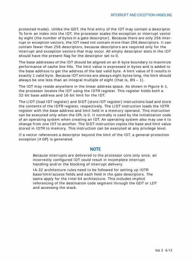
INTERRUPT AND EXCEPTION HANDLING
protected mode). Unlike the GDT, the first entry of the IDT may contain a descriptor. To form an index into the IDT, the processor scales the exception or interrupt vector by eight (the number of bytes in a gate descriptor). Because there are only 256 inter-rupt or exception vectors, the IDT need not contain more than 256 descriptors. It can contain fewer than 256 descriptors, because descriptors are required only for the interrupt and exception vectors that may occur. All empty descriptor slots in the IDT should have the present flag for the descriptor set to 0.
The base addresses of the IDT should be aligned on an 8-byte boundary to maximize performance of cache line fills. The limit value is expressed in bytes and is added to the base address to get the address of the last valid byte. A limit value of 0 results in exactly 1 valid byte. Because IDT entries are always eight bytes long, the limit should always be one less than an integral multiple of eight (that is, 8N – 1).
The IDT may reside anywhere in the linear address space. As shown in Figure 6-1, the processor locates the IDT using the IDTR register. This register holds both a 32-bit base address and 16-bit limit for the IDT.
The LIDT (load IDT register) and SIDT (store IDT register) instructions load and store the contents of the IDTR register, respectively. The LIDT instruction loads the IDTR register with the base address and limit held in a memory operand. This instruction can be executed only when the CPL is 0. It normally is used by the initialization code of an operating system when creating an IDT. An operating system also may use it to change from one IDT to another. The SIDT instruction copies the base and limit value stored in IDTR to memory. This instruction can be executed at any privilege level.
If a vector references a descriptor beyond the limit of the IDT, a general-protection exception (#GP) is generated.
NOTEBecause interrupts are delivered to the processor core only once, an incorrectly configured IDT could result in incomplete interrupt handling and/or the blocking of interrupt delivery.
IA-32 architecture rules need to be followed for setting up IDTR base/limit/access fields and each field in the gate descriptors. The same apply for the Intel 64 architecture. This includes implicit referencing of the destination code segment through the GDT or LDT and accessing the stack.
Vol. 3 6-13

INTERRUPT AND EXCEPTION HANDLING
6.11 IDT DESCRIPTORSThe IDT may contain any of three kinds of gate descriptors:
• Task-gate descriptor
• Interrupt-gate descriptor
• Trap-gate descriptor
Figure 6-2 shows the formats for the task-gate, interrupt-gate, and trap-gate descriptors. The format of a task gate used in an IDT is the same as that of a task gate used in the GDT or an LDT (see Section 7.2.5, “Task-Gate Descriptor”). The task gate contains the segment selector for a TSS for an exception and/or interrupt handler task.
Interrupt and trap gates are very similar to call gates (see Section 5.8.3, “Call Gates”). They contain a far pointer (segment selector and offset) that the processor uses to transfer program execution to a handler procedure in an exception- or inter-rupt-handler code segment. These gates differ in the way the processor handles the IF flag in the EFLAGS register (see Section 6.12.1.2, “Flag Usage By Exception- or Interrupt-Handler Procedure”).
Figure 6-1. Relationship of the IDTR and IDT
IDT LimitIDT Base Address
+Interrupt
Descriptor Table (IDT)Gate for
0IDTR Register
Interrupt #n
Gate forInterrupt #3
Gate forInterrupt #2
Gate forInterrupt #1
151647
0310
8
16
(n−1)∗8
6-14 Vol. 3
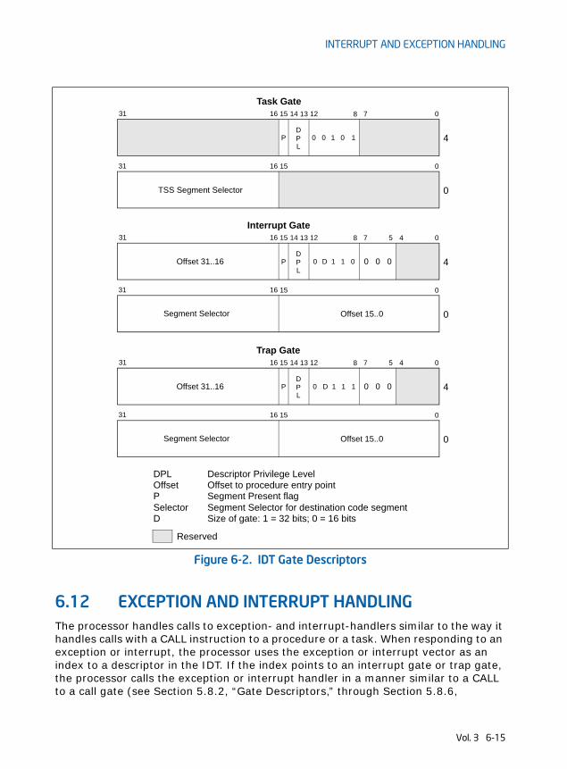
INTERRUPT AND EXCEPTION HANDLING
6.12 EXCEPTION AND INTERRUPT HANDLINGThe processor handles calls to exception- and interrupt-handlers similar to the way it handles calls with a CALL instruction to a procedure or a task. When responding to an exception or interrupt, the processor uses the exception or interrupt vector as an index to a descriptor in the IDT. If the index points to an interrupt gate or trap gate, the processor calls the exception or interrupt handler in a manner similar to a CALL to a call gate (see Section 5.8.2, “Gate Descriptors,” through Section 5.8.6,
Figure 6-2. IDT Gate Descriptors
31 16 15 1314 12 8 7 0
POffset 31..16DPL
0 4
31 16 15 0
Segment Selector Offset 15..0 0
011D
Interrupt Gate
DPLOffsetPSelector
Descriptor Privilege LevelOffset to procedure entry pointSegment Present flagSegment Selector for destination code segment
31 16 15 1314 12 8 7 0
PDPL
0 4
31 16 15 0
TSS Segment Selector 0
1010
Task Gate
45
0 0 0
31 16 15 1314 12 8 7 0
POffset 31..16DPL
0 4
31 16 15 0
Segment Selector Offset 15..0 0
111D
Trap Gate45
0 0 0
Reserved
Size of gate: 1 = 32 bits; 0 = 16 bitsD
Vol. 3 6-15

INTERRUPT AND EXCEPTION HANDLING
“Returning from a Called Procedure”). If index points to a task gate, the processor executes a task switch to the exception- or interrupt-handler task in a manner similar to a CALL to a task gate (see Section 7.3, “Task Switching”).
6.12.1 Exception- or Interrupt-Handler ProceduresAn interrupt gate or trap gate references an exception- or interrupt-handler proce-dure that runs in the context of the currently executing task (see Figure 6-3). The segment selector for the gate points to a segment descriptor for an executable code segment in either the GDT or the current LDT. The offset field of the gate descriptor points to the beginning of the exception- or interrupt-handling procedure.
Figure 6-3. Interrupt Procedure Call
IDT
Interrupt or
Code Segment
Segment Selector
GDT or LDT
Segment
InterruptVector
BaseAddress
Destination
ProcedureInterrupt
+
Descriptor
Trap Gate
Offset
6-16 Vol. 3

INTERRUPT AND EXCEPTION HANDLING
When the processor performs a call to the exception- or interrupt-handler procedure:
• If the handler procedure is going to be executed at a numerically lower privilege level, a stack switch occurs. When the stack switch occurs:
a. The segment selector and stack pointer for the stack to be used by the handler are obtained from the TSS for the currently executing task. On this new stack, the processor pushes the stack segment selector and stack pointer of the interrupted procedure.
b. The processor then saves the current state of the EFLAGS, CS, and EIP registers on the new stack (see Figures 6-4).
c. If an exception causes an error code to be saved, it is pushed on the new stack after the EIP value.
• If the handler procedure is going to be executed at the same privilege level as the interrupted procedure:
a. The processor saves the current state of the EFLAGS, CS, and EIP registers on the current stack (see Figures 6-4).
b. If an exception causes an error code to be saved, it is pushed on the current stack after the EIP value.
Vol. 3 6-17

INTERRUPT AND EXCEPTION HANDLING
To return from an exception- or interrupt-handler procedure, the handler must use the IRET (or IRETD) instruction. The IRET instruction is similar to the RET instruction except that it restores the saved flags into the EFLAGS register. The IOPL field of the EFLAGS register is restored only if the CPL is 0. The IF flag is changed only if the CPL is less than or equal to the IOPL. See Chapter 3, “Instruction Set Reference, A-M,” of the Intel® 64 and IA-32 Architectures Software Developer’s Manual, Volume 2A, for a description of the complete operation performed by the IRET instruction.
If a stack switch occurred when calling the handler procedure, the IRET instruction switches back to the interrupted procedure’s stack on the return.
6.12.1.1 Protection of Exception- and Interrupt-Handler ProceduresThe privilege-level protection for exception- and interrupt-handler procedures is similar to that used for ordinary procedure calls when called through a call gate (see Section 5.8.4, “Accessing a Code Segment Through a Call Gate”). The processor does
Figure 6-4. Stack Usage on Transfers to Interrupt and Exception-Handling Routines
CS
Error Code
EFLAGSCS
EIPESP AfterTransfer to Handler
Error Code
ESP BeforeTransfer to Handler
EFLAGS
EIP
SS ESP
Stack Usage with NoPrivilege-Level Change
Stack Usage withPrivilege-Level Change
Interrupted Procedure’s
Interrupted Procedure’sand Handler’s Stack
Handler’s Stack
ESP AfterTransfer to Handler
Transfer to HandlerESP Before
Stack
6-18 Vol. 3

INTERRUPT AND EXCEPTION HANDLING
not permit transfer of execution to an exception- or interrupt-handler procedure in a less privileged code segment (numerically greater privilege level) than the CPL.
An attempt to violate this rule results in a general-protection exception (#GP). The protection mechanism for exception- and interrupt-handler procedures is different in the following ways:
• Because interrupt and exception vectors have no RPL, the RPL is not checked on implicit calls to exception and interrupt handlers.
• The processor checks the DPL of the interrupt or trap gate only if an exception or interrupt is generated with an INT n, INT 3, or INTO instruction. Here, the CPL must be less than or equal to the DPL of the gate. This restriction prevents application programs or procedures running at privilege level 3 from using a software interrupt to access critical exception handlers, such as the page-fault handler, providing that those handlers are placed in more privileged code segments (numerically lower privilege level). For hardware-generated interrupts and processor-detected exceptions, the processor ignores the DPL of interrupt and trap gates.
Because exceptions and interrupts generally do not occur at predictable times, these privilege rules effectively impose restrictions on the privilege levels at which excep-tion and interrupt- handling procedures can run. Either of the following techniques can be used to avoid privilege-level violations.
• The exception or interrupt handler can be placed in a conforming code segment. This technique can be used for handlers that only need to access data available on the stack (for example, divide error exceptions). If the handler needs data from a data segment, the data segment needs to be accessible from privilege level 3, which would make it unprotected.
• The handler can be placed in a nonconforming code segment with privilege level 0. This handler would always run, regardless of the CPL that the interrupted program or task is running at.
6.12.1.2 Flag Usage By Exception- or Interrupt-Handler ProcedureWhen accessing an exception or interrupt handler through either an interrupt gate or a trap gate, the processor clears the TF flag in the EFLAGS register after it saves the contents of the EFLAGS register on the stack. (On calls to exception and interrupt handlers, the processor also clears the VM, RF, and NT flags in the EFLAGS register, after they are saved on the stack.) Clearing the TF flag prevents instruction tracing from affecting interrupt response. A subsequent IRET instruction restores the TF (and VM, RF, and NT) flags to the values in the saved contents of the EFLAGS register on the stack.
The only difference between an interrupt gate and a trap gate is the way the processor handles the IF flag in the EFLAGS register. When accessing an exception- or interrupt-handling procedure through an interrupt gate, the processor clears the IF flag to prevent other interrupts from interfering with the current interrupt handler. A subsequent IRET instruction restores the IF flag to its value in the saved contents
Vol. 3 6-19

INTERRUPT AND EXCEPTION HANDLING
of the EFLAGS register on the stack. Accessing a handler procedure through a trap gate does not affect the IF flag.
6.12.2 Interrupt TasksWhen an exception or interrupt handler is accessed through a task gate in the IDT, a task switch results. Handling an exception or interrupt with a separate task offers several advantages:
• The entire context of the interrupted program or task is saved automatically.
• A new TSS permits the handler to use a new privilege level 0 stack when handling the exception or interrupt. If an exception or interrupt occurs when the current privilege level 0 stack is corrupted, accessing the handler through a task gate can prevent a system crash by providing the handler with a new privilege level 0 stack.
• The handler can be further isolated from other tasks by giving it a separate address space. This is done by giving it a separate LDT.
The disadvantage of handling an interrupt with a separate task is that the amount of machine state that must be saved on a task switch makes it slower than using an interrupt gate, resulting in increased interrupt latency.
A task gate in the IDT references a TSS descriptor in the GDT (see Figure 6-5). A switch to the handler task is handled in the same manner as an ordinary task switch (see Section 7.3, “Task Switching”). The link back to the interrupted task is stored in the previous task link field of the handler task’s TSS. If an exception caused an error code to be generated, this error code is copied to the stack of the new task.
When exception- or interrupt-handler tasks are used in an operating system, there are actually two mechanisms that can be used to dispatch tasks: the software sched-uler (part of the operating system) and the hardware scheduler (part of the processor's interrupt mechanism). The software scheduler needs to accommodate interrupt tasks that may be dispatched when interrupts are enabled.
NOTEBecause IA-32 architecture tasks are not re-entrant, an interrupt-handler task must disable interrupts between the time it completes handling the interrupt and the time it executes the IRET instruction. This action prevents another interrupt from occurring while the interrupt task’s TSS is still marked busy, which would cause a general-protection (#GP) exception.
6-20 Vol. 3

INTERRUPT AND EXCEPTION HANDLING
6.13 ERROR CODEWhen an exception condition is related to a specific segment, the processor pushes an error code onto the stack of the exception handler (whether it is a procedure or task). The error code has the format shown in Figure 6-6. The error code resembles a segment selector; however, instead of a TI flag and RPL field, the error code contains 3 flags:
EXT External event (bit 0) — When set, indicates that an event external to the program, such as a hardware interrupt, caused the exception.
IDT Descriptor location (bit 1) — When set, indicates that the index portion of the error code refers to a gate descriptor in the IDT; when
Figure 6-5. Interrupt Task Switch
IDT
Task Gate
TSS for Interrupt-
TSS Selector
GDT
TSS Descriptor
InterruptVector
TSSBaseAddress
Handling Task
Vol. 3 6-21
CHAPTER 7TASK MANAGEMENT
This chapter describes the IA-32 architecture’s task management facilities. These facilities are only available when the processor is running in protected mode.
This chapter focuses on 32-bit tasks and the 32-bit TSS structure. For information on 16-bit tasks and the 16-bit TSS structure, see Section 7.6, “16-Bit Task-State Segment (TSS).” For information specific to task management in 64-bit mode, see Section 7.7, “Task Management in 64-bit Mode.”
7.1 TASK MANAGEMENT OVERVIEWA task is a unit of work that a processor can dispatch, execute, and suspend. It can be used to execute a program, a task or process, an operating-system service utility, an interrupt or exception handler, or a kernel or executive utility.
The IA-32 architecture provides a mechanism for saving the state of a task, for dispatching tasks for execution, and for switching from one task to another. When operating in protected mode, all processor execution takes place from within a task. Even simple systems must define at least one task. More complex systems can use the processor’s task management facilities to support multitasking applications.
7.1.1 Task StructureA task is made up of two parts: a task execution space and a task-state segment (TSS). The task execution space consists of a code segment, a stack segment, and one or more data segments (see Figure 7-1). If an operating system or executive uses the processor’s privilege-level protection mechanism, the task execution space also provides a separate stack for each privilege level.
The TSS specifies the segments that make up the task execution space and provides a storage place for task state information. In multitasking systems, the TSS also provides a mechanism for linking tasks.
A task is identified by the segment selector for its TSS. When a task is loaded into the processor for execution, the segment selector, base address, limit, and segment descriptor attributes for the TSS are loaded into the task register (see Section 2.4.4, “Task Register (TR)”).
If paging is implemented for the task, the base address of the page directory used by the task is loaded into control register CR3.
Vol. 3 7-1

TASK MANAGEMENT
7.1.2 Task StateThe following items define the state of the currently executing task:
• The task’s current execution space, defined by the segment selectors in the segment registers (CS, DS, SS, ES, FS, and GS).
• The state of the general-purpose registers.
• The state of the EFLAGS register.
• The state of the EIP register.
• The state of control register CR3.
• The state of the task register.
• The state of the LDTR register.
• The I/O map base address and I/O map (contained in the TSS).
• Stack pointers to the privilege 0, 1, and 2 stacks (contained in the TSS).
• Link to previously executed task (contained in the TSS).
Prior to dispatching a task, all of these items are contained in the task’s TSS, except the state of the task register. Also, the complete contents of the LDTR register are not contained in the TSS, only the segment selector for the LDT.
Figure 7-1. Structure of a Task
CodeSegment
StackSegment
(Current Priv.
DataSegment
Stack Seg.Priv. Level 0
Stack Seg.Priv. Level 1
StackSegment
(Priv. Level 2)
Task-StateSegment
(TSS)
Task Register
CR3
Level)
7-2 Vol. 3

TASK MANAGEMENT
7.1.3 Executing a TaskSoftware or the processor can dispatch a task for execution in one of the following ways:
• A explicit call to a task with the CALL instruction.
• A explicit jump to a task with the JMP instruction.
• An implicit call (by the processor) to an interrupt-handler task.
• An implicit call to an exception-handler task.
• A return (initiated with an IRET instruction) when the NT flag in the EFLAGS register is set.
All of these methods for dispatching a task identify the task to be dispatched with a segment selector that points to a task gate or the TSS for the task. When dispatching a task with a CALL or JMP instruction, the selector in the instruction may select the TSS directly or a task gate that holds the selector for the TSS. When dispatching a task to handle an interrupt or exception, the IDT entry for the interrupt or exception must contain a task gate that holds the selector for the interrupt- or exception-handler TSS.
When a task is dispatched for execution, a task switch occurs between the currently running task and the dispatched task. During a task switch, the execution environ-ment of the currently executing task (called the task’s state or context) is saved in its TSS and execution of the task is suspended. The context for the dispatched task is then loaded into the processor and execution of that task begins with the instruction pointed to by the newly loaded EIP register. If the task has not been run since the system was last initialized, the EIP will point to the first instruction of the task’s code; otherwise, it will point to the next instruction after the last instruction that the task executed when it was last active.
If the currently executing task (the calling task) called the task being dispatched (the called task), the TSS segment selector for the calling task is stored in the TSS of the called task to provide a link back to the calling task.
For all IA-32 processors, tasks are not recursive. A task cannot call or jump to itself.
Interrupts and exceptions can be handled with a task switch to a handler task. Here, the processor performs a task switch to handle the interrupt or exception and auto-matically switches back to the interrupted task upon returning from the interrupt-handler task or exception-handler task. This mechanism can also handle interrupts that occur during interrupt tasks.
As part of a task switch, the processor can also switch to another LDT, allowing each task to have a different logical-to-physical address mapping for LDT-based segments. The page-directory base register (CR3) also is reloaded on a task switch, allowing each task to have its own set of page tables. These protection facilities help isolate tasks and prevent them from interfering with one another.
If protection mechanisms are not used, the processor provides no protection between tasks. This is true even with operating systems that use multiple privilege levels for protection. A task running at privilege level 3 that uses the same LDT and
Vol. 3 7-3

TASK MANAGEMENT
page tables as other privilege-level-3 tasks can access code and corrupt data and the stack of other tasks.
Use of task management facilities for handling multitasking applications is optional. Multitasking can be handled in software, with each software defined task executed in the context of a single IA-32 architecture task.
7.2 TASK MANAGEMENT DATA STRUCTURESThe processor defines five data structures for handling task-related activities:
• Task-state segment (TSS).
• Task-gate descriptor.
• TSS descriptor.
• Task register.
• NT flag in the EFLAGS register.
When operating in protected mode, a TSS and TSS descriptor must be created for at least one task, and the segment selector for the TSS must be loaded into the task register (using the LTR instruction).
7.2.1 Task-State Segment (TSS)The processor state information needed to restore a task is saved in a system segment called the task-state segment (TSS). Figure 7-2 shows the format of a TSS for tasks designed for 32-bit CPUs. The fields of a TSS are divided into two main cate-gories: dynamic fields and static fields.
For information about 16-bit Intel 286 processor task structures, see Section 7.6, “16-Bit Task-State Segment (TSS).” For information about 64-bit mode task struc-tures, see Section 7.7, “Task Management in 64-bit Mode.”
7-4 Vol. 3
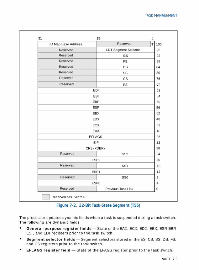
TASK MANAGEMENT
The processor updates dynamic fields when a task is suspended during a task switch. The following are dynamic fields:
• General-purpose register fields — State of the EAX, ECX, EDX, EBX, ESP, EBP, ESI, and EDI registers prior to the task switch.
• Segment selector fields — Segment selectors stored in the ES, CS, SS, DS, FS, and GS registers prior to the task switch.
• EFLAGS register field — State of the EFAGS register prior to the task switch.
Figure 7-2. 32-Bit Task-State Segment (TSS)
031
100
96
92
88
84
80
76
I/O Map Base Address
15
LDT Segment Selector
GS
FS
DS
SS
CS
72
68
64
60
56
52
48
44
40
36
32
28
24
20
SS2
16
12
8
4
0
SS1
SS0
ESP0
Previous Task Link
ESP1
ESP2
CR3 (PDBR)
T
ES
EDI
ESIEBP
ESP
EBX
EDX
ECX
EAX
EFLAGS
EIP
Reserved bits. Set to 0.
Reserved
Reserved
Reserved
Reserved
Reserved
Reserved
ReservedReserved
Reserved
Reserved
Reserved
Reserved
Vol. 3 7-5

TASK MANAGEMENT
• EIP (instruction pointer) field — State of the EIP register prior to the task switch.
• Previous task link field — Contains the segment selector for the TSS of the previous task (updated on a task switch that was initiated by a call, interrupt, or exception). This field (which is sometimes called the back link field) permits a task switch back to the previous task by using the IRET instruction.
The processor reads the static fields, but does not normally change them. These fields are set up when a task is created. The following are static fields:
• LDT segment selector field — Contains the segment selector for the task's LDT.
• CR3 control register field — Contains the base physical address of the page directory to be used by the task. Control register CR3 is also known as the page-directory base register (PDBR).
• Privilege level-0, -1, and -2 stack pointer fields — These stack pointers consist of a logical address made up of the segment selector for the stack segment (SS0, SS1, and SS2) and an offset into the stack (ESP0, ESP1, and ESP2). Note that the values in these fields are static for a particular task; whereas, the SS and ESP values will change if stack switching occurs within the task.
• T (debug trap) flag (byte 100, bit 0) — When set, the T flag causes the processor to raise a debug exception when a task switch to this task occurs (see Section 16.3.1.5, “Task-Switch Exception Condition”).
• I/O map base address field — Contains a 16-bit offset from the base of the TSS to the I/O permission bit map and interrupt redirection bitmap. When present, these maps are stored in the TSS at higher addresses. The I/O map base address points to the beginning of the I/O permission bit map and the end of the interrupt redirection bit map. See Chapter 13, “Input/Output,” in the Intel® 64 and IA-32 Architectures Software Developer’s Manual, Volume 1, for more information about the I/O permission bit map. See Section 17.3, “Interrupt and Exception Handling in Virtual-8086 Mode,” for a detailed description of the interrupt redirection bit map.
If paging is used:
• Avoid placing a page boundary in the part of the TSS that the processor reads during a task switch (the first 104 bytes). The processor may not correctly perform address translations if a boundary occurs in this area. During a task switch, the processor reads and writes into the first 104 bytes of each TSS (using contiguous physical addresses beginning with the physical address of the first byte of the TSS). So, after TSS access begins, if part of the 104 bytes is not physically contiguous, the processor will access incorrect information without generating a page-fault exception.
• Pages corresponding to the previous task’s TSS, the current task’s TSS, and the descriptor table entries for each all should be marked as read/write.
7-6 Vol. 3

TASK MANAGEMENT
• Task switches are carried out faster if the pages containing these structures are present in memory before the task switch is initiated.
7.2.2 TSS DescriptorThe TSS, like all other segments, is defined by a segment descriptor. Figure 7-3 shows the format of a TSS descriptor. TSS descriptors may only be placed in the GDT; they cannot be placed in an LDT or the IDT.
An attempt to access a TSS using a segment selector with its TI flag set (which indi-cates the current LDT) causes a general-protection exception (#GP) to be generated during CALLs and JMPs; it causes an invalid TSS exception (#TS) during IRETs. A general-protection exception is also generated if an attempt is made to load a segment selector for a TSS into a segment register.
The busy flag (B) in the type field indicates whether the task is busy. A busy task is currently running or suspended. A type field with a value of 1001B indicates an inac-tive task; a value of 1011B indicates a busy task. Tasks are not recursive. The processor uses the busy flag to detect an attempt to call a task whose execution has been interrupted. To insure that there is only one busy flag is associated with a task, each TSS should have only one TSS descriptor that points to it.
The base, limit, and DPL fields and the granularity and present flags have functions similar to their use in data-segment descriptors (see Section 3.4.5, “Segment Descriptors”). When the G flag is 0 in a TSS descriptor for a 32-bit TSS, the limit field must have a value equal to or greater than 67H, one byte less than the minimum size
Figure 7-3. TSS Descriptor
31 24 23 22 21 20 19 16 15 1314 12 11 8 7 0
PBase 31:24 GDPL
Type
00
31 16 15 0
Base Address 15:00 Segment Limit 15:00
Base 23:16AVL
Limit19:160
1B01
TSS Descriptor
AVLBBASEDPLG
Available for use by system softwareBusy flagSegment Base AddressDescriptor Privilege LevelGranularity
LIMITPTYPE
Segment LimitSegment PresentSegment Type
0
4
Vol. 3 7-7

TASK MANAGEMENT
of a TSS. Attempting to switch to a task whose TSS descriptor has a limit less than 67H generates an invalid-TSS exception (#TS). A larger limit is required if an I/O permission bit map is included or if the operating system stores additional data. The processor does not check for a limit greater than 67H on a task switch; however, it does check when accessing the I/O permission bit map or interrupt redirection bit map.
Any program or procedure with access to a TSS descriptor (that is, whose CPL is numerically equal to or less than the DPL of the TSS descriptor) can dispatch the task with a call or a jump.
In most systems, the DPLs of TSS descriptors are set to values less than 3, so that only privileged software can perform task switching. However, in multitasking appli-cations, DPLs for some TSS descriptors may be set to 3 to allow task switching at the application (or user) privilege level.
7.2.3 TSS Descriptor in 64-bit modeIn 64-bit mode, task switching is not supported, but TSS descriptors still exist. The format of a 64-bit TSS is described in Section 7.7.
In 64-bit mode, the TSS descriptor is expanded to 16 bytes (see Figure 7-4). This expansion also applies to an LDT descriptor in 64-bit mode. Table 3-2 provides the encoding information for the segment type field.
7-8 Vol. 3

TASK MANAGEMENT
7.2.4 Task RegisterThe task register holds the 16-bit segment selector and the entire segment descriptor (32-bit base address, 16-bit segment limit, and descriptor attributes) for the TSS of the current task (see Figure 2-5). This information is copied from the TSS descriptor in the GDT for the current task. Figure 7-5 shows the path the processor uses to access the TSS (using the information in the task register).
The task register has a visible part (that can be read and changed by software) and an invisible part (maintained by the processor and is inaccessible by software). The segment selector in the visible portion points to a TSS descriptor in the GDT. The processor uses the invisible portion of the task register to cache the segment descriptor for the TSS. Caching these values in a register makes execution of the task more efficient. The LTR (load task register) and STR (store task register) instructions load and read the visible portion of the task register:
Figure 7-4. Format of TSS and LDT Descriptors in 64-bit Mode
31 24 23 22 21 20 19 16 15 1314 12 11 8 7 0
PBase 31:24 GDPL
Type
00
31 16 15 0
Base Address 15:00 Segment Limit 15:00
Base 23:16AVL
Limit19:160
TSS (or LDT) Descriptor
AVLBBASEDPLG
Available for use by system softwareBusy flagSegment Base AddressDescriptor Privilege LevelGranularity
LIMITPTYPE
Segment LimitSegment PresentSegment Type
0
4
31 13 12 8 7 0
Reserved
31 0
Base Address 63:32
Reserved0
8
12
Vol. 3 7-9

TASK MANAGEMENT
The LTR instruction loads a segment selector (source operand) into the task register that points to a TSS descriptor in the GDT. It then loads the invisible portion of the task register with information from the TSS descriptor. LTR is a privileged instruction that may be executed only when the CPL is 0. It’s used during system initialization to put an initial value in the task register. Afterwards, the contents of the task register are changed implicitly when a task switch occurs.
The STR (store task register) instruction stores the visible portion of the task register in a general-purpose register or memory. This instruction can be executed by code running at any privilege level in order to identify the currently running task. However, it is normally used only by operating system software.
On power up or reset of the processor, segment selector and base address are set to the default value of 0; the limit is set to FFFFH.
Figure 7-5. Task Register
Segment LimitSelector
+
GDT
TSS Descriptor
0
Base AddressTaskInvisible PartVisible Part
TSS
Register
7-10 Vol. 3

TASK MANAGEMENT
7.2.5 Task-Gate DescriptorA task-gate descriptor provides an indirect, protected reference to a task (see Figure 7-6). It can be placed in the GDT, an LDT, or the IDT. The TSS segment selector field in a task-gate descriptor points to a TSS descriptor in the GDT. The RPL in this segment selector is not used.
The DPL of a task-gate descriptor controls access to the TSS descriptor during a task switch. When a program or procedure makes a call or jump to a task through a task gate, the CPL and the RPL field of the gate selector pointing to the task gate must be less than or equal to the DPL of the task-gate descriptor. Note that when a task gate is used, the DPL of the destination TSS descriptor is not used.
A task can be accessed either through a task-gate descriptor or a TSS descriptor. Both of these structures satisfy the following needs:
• Need for a task to have only one busy flag — Because the busy flag for a task is stored in the TSS descriptor, each task should have only one TSS descriptor. There may, however, be several task gates that reference the same TSS descriptor.
• Need to provide selective access to tasks — Task gates fill this need, because they can reside in an LDT and can have a DPL that is different from the TSS descriptor's DPL. A program or procedure that does not have sufficient privilege to access the TSS descriptor for a task in the GDT (which usually has a DPL of 0) may be allowed access to the task through a task gate with a higher DPL. Task gates give the operating system greater latitude for limiting access to specific tasks.
• Need for an interrupt or exception to be handled by an independent task — Task gates may also reside in the IDT, which allows interrupts and exceptions
Figure 7-6. Task-Gate Descriptor
31 16 15 1314 12 11 8 7 0
PDPL
Type
0
31 16 15 0
TSS Segment Selector
1010
DPLPTYPE
Descriptor Privilege LevelSegment PresentSegment Type
4
0Reserved
ReservedReserved
Vol. 3 7-11

TASK MANAGEMENT
to be handled by handler tasks. When an interrupt or exception vector points to a task gate, the processor switches to the specified task.
Figure 7-7 illustrates how a task gate in an LDT, a task gate in the GDT, and a task gate in the IDT can all point to the same task.
7.3 TASK SWITCHINGThe processor transfers execution to another task in one of four cases:
• The current program, task, or procedure executes a JMP or CALL instruction to a TSS descriptor in the GDT.
• The current program, task, or procedure executes a JMP or CALL instruction to a task-gate descriptor in the GDT or the current LDT.
Figure 7-7. Task Gates Referencing the Same Task
LDT
Task Gate
TSSGDT
TSS Descriptor
IDT
Task Gate
Task Gate
7-12 Vol. 3

TASK MANAGEMENT
• An interrupt or exception vector points to a task-gate descriptor in the IDT.
• The current task executes an IRET when the NT flag in the EFLAGS register is set.
JMP, CALL, and IRET instructions, as well as interrupts and exceptions, are all mech-anisms for redirecting a program. The referencing of a TSS descriptor or a task gate (when calling or jumping to a task) or the state of the NT flag (when executing an IRET instruction) determines whether a task switch occurs.
The processor performs the following operations when switching to a new task:
1. Obtains the TSS segment selector for the new task as the operand of the JMP or CALL instruction, from a task gate, or from the previous task link field (for a task switch initiated with an IRET instruction).
2. Checks that the current (old) task is allowed to switch to the new task. Data-access privilege rules apply to JMP and CALL instructions. The CPL of the current (old) task and the RPL of the segment selector for the new task must be less than or equal to the DPL of the TSS descriptor or task gate being referenced. Exceptions, interrupts (except for interrupts generated by the INT n instruction), and the IRET instruction are permitted to switch tasks regardless of the DPL of the destination task-gate or TSS descriptor. For interrupts generated by the INT n instruction, the DPL is checked.
3. Checks that the TSS descriptor of the new task is marked present and has a valid limit (greater than or equal to 67H).
4. Checks that the new task is available (call, jump, exception, or interrupt) or busy (IRET return).
5. Checks that the current (old) TSS, new TSS, and all segment descriptors used in the task switch are paged into system memory.
6. If the task switch was initiated with a JMP or IRET instruction, the processor clears the busy (B) flag in the current (old) task’s TSS descriptor; if initiated with a CALL instruction, an exception, or an interrupt: the busy (B) flag is left set. (See Table 7-2.)
7. If the task switch was initiated with an IRET instruction, the processor clears the NT flag in a temporarily saved image of the EFLAGS register; if initiated with a CALL or JMP instruction, an exception, or an interrupt, the NT flag is left unchanged in the saved EFLAGS image.
8. Saves the state of the current (old) task in the current task’s TSS. The processor finds the base address of the current TSS in the task register and then copies the states of the following registers into the current TSS: all the general-purpose registers, segment selectors from the segment registers, the temporarily saved image of the EFLAGS register, and the instruction pointer register (EIP).
9. If the task switch was initiated with a CALL instruction, an exception, or an interrupt, the processor will set the NT flag in the EFLAGS loaded from the new task. If initiated with an IRET instruction or JMP instruction, the NT flag will reflect the state of NT in the EFLAGS loaded from the new task (see Table 7-2).
Vol. 3 7-13

TASK MANAGEMENT
10. If the task switch was initiated with a CALL instruction, JMP instruction, an exception, or an interrupt, the processor sets the busy (B) flag in the new task’s TSS descriptor; if initiated with an IRET instruction, the busy (B) flag is left set.
11. Loads the task register with the segment selector and descriptor for the new task's TSS.
12. The TSS state is loaded into the processor. This includes the LDTR register, the PDBR (control register CR3), the EFLAGS registers, the EIP register, the general-purpose registers, and the segment selectors. Note that a fault during the load of this state may corrupt architectural state.
13. The descriptors associated with the segment selectors are loaded and qualified. Any errors associated with this loading and qualification occur in the context of the new task.
NOTESIf all checks and saves have been carried out successfully, the processor commits to the task switch. If an unrecoverable error occurs in steps 1 through 11, the processor does not complete the task switch and insures that the processor is returned to its state prior to the execution of the instruction that initiated the task switch.
If an unrecoverable error occurs in step 12, architectural state may be corrupted, but an attempt will be made to handle the error in the prior execution environment. If an unrecoverable error occurs after the commit point (in step 13), the processor completes the task switch (without performing additional access and segment avail-ability checks) and generates the appropriate exception prior to beginning execution of the new task.
If exceptions occur after the commit point, the exception handler must finish the task switch itself before allowing the processor to begin executing the new task. See Chapter 6, “Interrupt 10—Invalid TSS Exception (#TS),” for more information about the affect of exceptions on a task when they occur after the commit point of a task switch.
14. Begins executing the new task. (To an exception handler, the first instruction of the new task appears not to have been executed.)
The state of the currently executing task is always saved when a successful task switch occurs. If the task is resumed, execution starts with the instruction pointed to by the saved EIP value, and the registers are restored to the values they held when the task was suspended.
When switching tasks, the privilege level of the new task does not inherit its privilege level from the suspended task. The new task begins executing at the privilege level specified in the CPL field of the CS register, which is loaded from the TSS. Because tasks are isolated by their separate address spaces and TSSs and because privilege
7-14 Vol. 3

TASK MANAGEMENT
The TS (task switched) flag in the control register CR0 is set every time a task switch occurs. System software uses the TS flag to coordinate the actions of floating-point unit when generating floating-point exceptions with the rest of the processor. The TS flag indicates that the context of the floating-point unit may be different from that of the current task. See Section 2.5, “Control Registers”, for a detailed description of the function and use of the TS flag.
7.4 TASK LINKINGThe previous task link field of the TSS (sometimes called the “backlink”) and the NT flag in the EFLAGS register are used to return execution to the previous task. EFLAGS.NT = 1 indicates that the currently executing task is nested within the execution of another task.
When a CALL instruction, an interrupt, or an exception causes a task switch: the processor copies the segment selector for the current TSS to the previous task link field of the TSS for the new task; it then sets EFLAGS.NT = 1. If software uses an IRET instruction to suspend the new task, the processor checks for EFLAGS.NT = 1; it then uses the value in the previous task link field to return to the previous task. See Figures 7-8.
When a JMP instruction causes a task switch, the new task is not nested. The previous task link field is not used and EFLAGS.NT = 0. Use a JMP instruction to dispatch a new task when nesting is not desired.
DS, ES, FS, and GS segments are present in memory. #NP New Data Segment
DS, ES, FS, and GS segment DPL greater than or equal to CPL (unless these are conforming segments).
#TS New Data Segment
NOTES:1. #NP is segment-not-present exception, #GP is general-protection exception, #TS is invalid-TSS
exception, and #SS is stack-fault exception.2. The error code contains an index to the segment descriptor referenced in this column.3. A segment selector is valid if it is in a compatible type of table (GDT or LDT), occupies an address
within the table's segment limit, and refers to a compatible type of descriptor (for example, a seg-ment selector in the CS register only is valid when it points to a code-segment descriptor).
Table 7-1. Exception Conditions Checked During a Task Switch (Contd.)Condition Checked Exception1 Error Code
Reference2
7-16 Vol. 3

TASK MANAGEMENT
Table 7-2 shows the busy flag (in the TSS segment descriptor), the NT flag, the previous task link field, and TS flag (in control register CR0) during a task switch.
The NT flag may be modified by software executing at any privilege level. It is possible for a program to set the NT flag and execute an IRET instruction. This might randomly invoke the task specified in the previous link field of the current task's TSS. To keep such spurious task switches from succeeding, the operating system should initialize the previous task link field in every TSS that it creates to 0.
Figure 7-8. Nested Tasks
Table 7-2. Effect of a Task Switch on Busy Flag, NT Flag, Previous Task Link Field, and TS Flag
Flag or Field Effect of JMP instruction
Effect of CALL Instruction or
Interrupt
Effect of IRETInstruction
Busy (B) flag of new task.
Flag is set. Must have been clear before.
Flag is set. Must have been clear before.
No change. Must have been set.
Busy flag of old task. Flag is cleared. No change. Flag is currently set.
Flag is cleared.
NT flag of new task. Set to value from TSS of new task.
Flag is set. Set to value from TSS of new task.
NT flag of old task. No change. No change. Flag is cleared.
Previous task link field of new task.
No change. Loaded with selector for old task’s TSS.
No change.
Previous task link field of old task.
No change. No change. No change.
TS flag in control register CR0.
Flag is set. Flag is set. Flag is set.
Top LevelTask
NT=0
Previous
TSS
NestedTask
NT=1
TSS
More DeeplyNested Task
NT=1
TSS
Currently ExecutingTask
NT=1EFLAGS
Task RegisterTask LinkPrevious
Task LinkPrevious
Task Link
Vol. 3 7-17