intel ixp1240 network processor - digi-key sheets/intel pdfs/ixp1240.pdf · the intel® ixp1240...
TRANSCRIPT

Intel® IXP1240 Network Processor
DatasheetProduct Features
The Intel® IXP1240 Network Processor delivers high-performance processing power and flexibility to a wide variety of LAN and telecommunications products. Distinguishing features of the IXP1240 are the performance of ASIC hardware along with programmability of a microprocessor.
■ Applications— Multi-layer LAN Switches— Multi-protocol Telecommunications Products— Broadband Cable Products— Remote Access Devices— Intelligent PCI adapters
■ Integrated StrongARM Core— High-performance, low-power, 32-bit
Embedded RISC processor— 16 Kbyte instruction cache— 8 Kbyte data cache— 512 byte mini-cache for data that is used once
and then discarded— Write buffer— Memory management unit— Access to IXP1240 FBI Unit, PCI Unit and
SDRAM Unit via the ARM* AMBA Bus
■ Six Integrated Programmable Microengines— Operating frequency of up to 232 MHz— Multi-thread support of four threads per
microengine— Single-cycle ALU and shift operations— Zero context swap overhead— Large Register Set: 128 General-Purpose and
128 Transfer Registers— 2 K x 32-bit Instruction Control Store— Access to the IXP1240 FBI Unit, PCI DMA
channels, SRAM, and SDRAM
■ High Bandwidth I/O Bus (IX Bus)— 64-bit, up to 104 MHz operation— 6.6 Gbps peak bandwidth— 64-bit or dual 32-bit bus options
■ Integrated 32-bit, 66 MHz PCI Interface— Supports PCI Local Bus Specification
Revision 2.2 as a Bus Master— 264 Mbytes/sec peak burst mode operation— I2O* support for StrongARM Core— Dual DMA channels
■ Industry Standard 64-bit SDRAM Interface— Peak bandwidth of up to 928 Mbytes/sec— Address up to 256 Mbytes of SDRAM— Memory bandwidth improvement through
bank switching— Read-modify-write support— Byte aligner/merger— Cyclic Redundancy Check (CRC)
■ Industry Standard 32-bit SRAM Interface— Peak bandwidth of up to 464 Mbytes/sec— Address up to 8 Mbytes of SRAM— Up to 8 Mbytes FlashROM for booting
StrongARM Core— Supports atomic push/pop operations— Supports atomic bit set and bit clear
operations— Memory bandwidth improvement by reduced
read/write turnaround bus cycles
■ Other Integrated Features— Hardware Hash Unit for generation of 48- or
64-bit adaptive polynomial hash keys— Serial UART port— Real Time Clock— Four general-purpose I/O pins— Four 24-bit timers with CPU watchdog
support— Limited JTAG Support— 4 Kbyte Scratchpad Memory
■ 432-pin, HL-PBGA package■ 2 V CMOS device
— 3.3 V tolerant I/O
Part Number: 278405-003December 2001
Notice: This document contains preliminary information on new products in production. The specifications are subject to change without notice. Verify with your local Intel sales office that you have the latest datasheet before finalizing a design.

Intel® IXP1240 Network Processor
ii
Information in this dproperty rights is grwhatsoever, and Intfitness for a particuintended for use in
Intel may make cha
Designers must notfuture definition and
The IXP1240 Netwospecifications. Curr
Contact your local I
Copies of documen1-800-548-4725 or
Copyright © Intel C
Intel is a registered
*Other names and b
Revision History
Date Revision Description
6/8/01 001 Advance Information Release.
8/10/01 002 Release for the V2.0 SDK.
12/10/01 003 Release for the V2.01 SDK.
Datasheet
ocument is provided in connection with Intel® products. No license, express or implied, by estoppel or otherwise, to any intellectual anted by this document. Except as provided in Intel’s Terms and Conditions of Sale for such products, Intel assumes no liability el disclaims any express or implied warranty, relating to sale and/or use of Intel products including liability or warranties relating to lar purpose, merchantability, or infringement of any patent, copyright or other intellectual property right. Intel products are not medical, life saving, or life sustaining applications.
nges to specifications and product descriptions at any time, without notice.
rely on the absence or characteristics of any features or instructions marked “reserved” or “undefined.” Intel reserves these for shall have no responsibility whatsoever for conflicts or incompatibilities arising from future changes to them.
rk Processor may contain design defects or errors known as errata which may cause the product to deviate from published ent characterized errata are available on request.
ntel sales office or your distributor to obtain the latest specifications and before placing your product order.
ts which have an ordering number and are referenced in this document, or other Intel literature may be obtained by calling by visiting Intel's website at http://www.intel.com.
orporation, 2001
trademark of Intel Corporation or its subsidiaries in the United States and other countries
rands may be claimed as the property of others.

Intel® IXP1240 Network Processor
Contents1.0 Product Description ............................................................................................................9
2.0 Functional Units................................................................................................................11
2.1 Conventions ........................................................................................................112.2 StrongARM* Core................................................................................................112.3 Microengines .......................................................................................................112.4 FBI Unit and the IX Bus.......................................................................................12
2.4.1 IX Bus Access Behavior .........................................................................122.4.1.1 Reset and Idle Bus Considerations ...........................................14
2.5 SDRAM and SRAM Units....................................................................................152.5.1 SDRAM Unit ...........................................................................................152.5.2 SDRAM Bus Access Behavior ...............................................................162.5.3 SDRAM Cyclic Redundancy Checking (CRC) .......................................172.5.4 SDRAM Configurations ..........................................................................182.5.5 SRAM Unit..............................................................................................18
2.5.5.1 SRAM Types Supported............................................................202.5.5.2 SRAM Configurations................................................................202.5.5.3 BootROM Configurations ..........................................................202.5.5.4 SRAM Bus Access Behavior .....................................................21
2.6 PCI Unit ...............................................................................................................222.6.1 PCI Arbitration and Central Function Support ........................................22
2.7 Device Reset .......................................................................................................232.7.1 Hardware Initiated Reset........................................................................252.7.2 Software Initiated Reset .........................................................................252.7.3 PCI Initiated Reset .................................................................................252.7.4 Watchdog Timer Initiated Reset .............................................................25
3.0 Signal Description ............................................................................................................26
3.1 Pinout Diagram....................................................................................................263.2 Pin Type Legend .................................................................................................273.3 Pin Description, Grouped by Function.................................................................28
3.3.1 Processor Support Pins..........................................................................283.3.2 SRAM Interface Pins ..............................................................................293.3.3 SDRAM Interface Pins ...........................................................................313.3.4 IX Bus Interface Pins..............................................................................333.3.5 General Purpose I/Os.............................................................................373.3.6 Serial Port (UART) Pins .........................................................................373.3.7 PCI Interface Pins ..................................................................................383.3.8 Power Supply Pins .................................................................................413.3.9 IEEE 1149.1 Interface Pins ....................................................................423.3.10 Miscellaneous Test Pins.........................................................................423.3.11 Pin Usage Summary ..............................................................................43
3.4 Pin/Signal List......................................................................................................443.5 Signals Listed in Alphabetical Order ...................................................................483.6 IX Bus Pins Function Listed by Operating Mode.................................................523.7 IX Bus Decode Table Listed by Operating Mode Type .......................................623.8 Pin State During Reset........................................................................................64
Datasheet iii
Intel® IXP1240 Network Processor
3.9 Pullup/Pulldown and Unused Pin Guidelines ...................................................... 66
4.0 Electrical Specifications ...................................................................................................67
4.1 Absolute Maximum Ratings ................................................................................ 674.2 DC Specifications................................................................................................ 70
4.2.1 Type 1 Driver DC Specifications ............................................................704.2.2 Type 2 Driver DC Specifications ............................................................714.2.3 Overshoot/Undershoot Specifications.................................................... 71
4.3 AC Specifications ................................................................................................ 724.3.1 Clock Timing Specifications ................................................................... 724.3.2 PXTAL Clock Input................................................................................. 724.3.3 PXTAL Clock Oscillator Specifications................................................... 734.3.4 PCI .........................................................................................................73
4.3.4.1 PCI Electrical Specification Conformance................................. 734.3.4.2 PCI Clock Signal AC Parameter Measurements....................... 734.3.4.3 PCI Bus Signals Timing............................................................. 75
4.3.5 Reset...................................................................................................... 764.3.5.1 Reset Timings Specification...................................................... 76
4.3.6 IEEE 1149.1 ........................................................................................... 774.3.6.1 IEEE 1149.1 Timing Specifications ........................................... 78
4.3.7 IX Bus..................................................................................................... 804.3.7.1 FCLK Signal AC Parameter Measurements.............................. 804.3.7.2 IX Bus Signals Timing ............................................................... 814.3.7.3 IX Bus Protocol.......................................................................... 834.3.7.4 RDYBus................................................................................... 1174.3.7.5 TK_IN/TK_OUT.......................................................................120
4.3.8 SRAM Interface....................................................................................1204.3.8.1 SRAM SCLK Signal AC Parameter Measurements ................ 1204.3.8.2 SRAM Bus Signal Timing........................................................ 1224.3.8.3 SRAM Bus - SRAM Signal Protocol and Timing ..................... 1244.3.8.4 SRAM Bus - BootROM and SlowPort Timings........................ 1294.3.8.5 SRAM Bus - BootRom Signal Protocol and Timing................. 1294.3.8.6 SRAM Bus - Slow-Port Device Signal Protocol and Timing.... 132
4.3.9 SDRAM Interface ................................................................................. 1364.3.9.1 SDCLK AC Parameter Measurements.................................... 1364.3.9.2 SDRAM Bus Signal Timing ..................................................... 1374.3.9.3 SDRAM Signal Protocol ..........................................................138
4.4 Asynchronous Signal Timing Descriptions........................................................ 143
5.0 Mechanical Specifications.............................................................................................. 144
5.1 Package Dimensions ........................................................................................ 1445.2 IXP1240 Package Dimensions (mm) ................................................................146
Figures1 Block Diagram....................................................................................................... 92 System Block Diagram........................................................................................ 103 SDRAM Unit Block Diagram ...............................................................................164 SRAM Unit Block Diagram .................................................................................. 195 Reset Logic .........................................................................................................246 Pinout Diagram ...................................................................................................26
iv Datasheet
Intel® IXP1240 Network Processor
7 64-Bit Bidirectional IX Bus, 1-2 MAC Mode.........................................................528 64-Bit Bidirectional IX Bus, 1-2 MAC Mode, FastPort Device .............................539 64-Bit Bidirectional IX Bus, 3+ MAC Mode..........................................................5510 32-Bit Unidirectional IX Bus, 1-2 MAC Mode ......................................................5811 32-bit Unidirectional IX Bus, 3+ MAC Mode (3-4 MACs Supported) ...................6012 Typical IXP1240 Heatsink Application.................................................................6913 PXTAL Clock Input ..............................................................................................7214 PCI Clock Signal AC Parameter Measurements.................................................7315 PCI Bus Signals ..................................................................................................7416 RESET_IN_L Timing Diagram ............................................................................7617 IEEE 1149.1/Boundary-Scan General Timing.....................................................7818 IEEE 1149.1/Boundary-Scan Tri-State Timing....................................................7919 FCLK Signal AC Parameter Measurements........................................................8020 IX Bus Signals Timing .........................................................................................8121 64-Bit Bidirectional IX Bus Timing, 1-2 MAC Mode, Consecutive Receive
and Transmit, No EOP ........................................................................................8322 64-Bit Bidirectional IX Bus Timing - Consecutive Receive and Transmit, No
EOP.....................................................................................................................8423 64-Bit Bidirectional IX Bus Timing - Consecutive Receive and Transmit,
EOP on 8th Data Return with Status...................................................................8524 64-Bit Bidirectional IX Bus Timing - Consecutive Receive and Transmit,
EOP on 7th Data Return with Status...................................................................8625 64-Bit Bidirectional IX Bus Timing - Consecutive Receive and Transmit,
EOP on 6th Data Return with Status...................................................................8726 64-Bit Bidirectional IX Bus Timing - Consecutive Receive and Transmit,
EOP on 5th Data Return with Status...................................................................8827 64-Bit Bidirectional IX Bus Timing - Consecutive Receive and Transmit,
EOP on 4th Data Return with Status...................................................................8928 64-Bit Bidirectional IX Bus Timing - Consecutive Receive and Transmit,
EOP on 1st through 3rd Data Return with Status (3rd Data Return Shown).......9029 64-Bit Bidirectional IX Bus Timing - Consecutive Receives, EOP on 1st Data
Return, No Status................................................................................................9130 64-Bit Bidirectional IX Bus Timing - Consecutive Receives, No EOP .................9231 64-Bit Bidirectional IX Bus Timing - Consecutive Receives, EOP on 8th Data
Return with Status ...............................................................................................9332 64-Bit Bidirectional IX Bus Timing - Consecutive Receives, EOP on 7th Data
Return with Status ...............................................................................................9433 64-Bit Bidirectional IX Bus Timing - Consecutive Receives, EOP on 6th Data
Return with Status ...............................................................................................9534 64-Bit Bidirectional IX Bus Timing - Consecutive Receives, EOP, Two
Element Transfer with Status ..............................................................................9635 64-Bit Bidirectional IX Bus Timing - Consecutive Receives, Fetch-9, No EOP...9736 64-Bit Bidirectional IX Bus Timing - Consecutive Transmits, EOP......................9837 64-Bit Bidirectional IX Bus Timing - Consecutive Transmits with Prepend, EOP9938 32-Bit Unidirectional IX Bus Timing - Consecutive Receives, No EOP.............10039 32-Bit Unidirectional IX Bus Timing - Consecutive Receives, EOP on 16th
Data Return with Status ....................................................................................10140 32-Bit Unidirectional IX Bus Timing - Consecutive Receives, EOP on 15th
Data Return with Status ....................................................................................10241 32-Bit Unidirectional IX Bus Timing - Consecutive Receives, EOP on 14th
Data Return with Status ....................................................................................103
Datasheet v
Intel® IXP1240 Network Processor
42 32-Bit Unidirectional IX Bus Timing - Consecutive Receives, EOP on 1st Through 13th Data Return with Status (13th Data Return Shown) ...................104
43 32-Bit Unidirectional IX Bus Timing - Consecutive Receives, EOP, 64-Bit Status ................................................................................................................ 105
44 32-Bit Unidirectional IX Bus Timing - Consecutive Receives, Two Element Transfers with 32-Bit Status .............................................................................. 106
45 32-Bit Unidirectional IX Bus Timing - Consecutive Transmits, EOP ................. 10746 32-Bit Unidirectional IX Bus Timing - Consecutive Transmits with Prepend,
EOP................................................................................................................... 10847 64-Bit Bidirectional IX Bus Timing - Consecutive FastPort Receives, Same
Port, EOP, No Status, FP_READY_WAIT=0 .................................................... 10948 64-Bit Bidirectional IX Bus Timing - Consecutive FastPort Receives, Same
Port, EOP, No Status, FP_READY_WAIT=5 .................................................... 11049 64-Bit Bidirectional IX Bus Timing - Consecutive FastPort Receives, Same
Port, EOP, with Status, FP_READY_WAIT=0 .................................................. 11150 64-Bit Bidirectional IX Bus Timing - Consecutive FastPort Receives, Same
Port, EOP, No Status, FP_READY_WAIT=5 .................................................... 11251 64-Bit Bidirectional IX Bus Timing - Consecutive FastPort Receives, Same
Port, EOP, No Status, FP_READY_WAIT=0, Cancelled Request.................... 11352 64-Bit Bidirectional IX Bus Timing - Consecutive FastPort Receives, Same
Port, No EOP, FP_READY_WAIT=Don’t Care ................................................. 11453 64-Bit Bidirectional IX Bus Timing - Consecutive FastPort Receives, Different
Ports, EOP, No Status, FP_READY_WAIT=0 .................................................. 11554 64-Bit Bidirectional IX Bus Timing - Consecutive FastPort Receives, Different
Ports, EOP, No Status, FP_READY_WAIT=0, Cancelled Request .................. 11655 Consecutive Fetch Ready Flags, 1-2 MAC Mode (with No External Registered
Decoder) - RDYBUS_TEMPLATE_CTL[10]=1 ................................................. 11756 Consecutive Fetch Ready Flags, 3+ MAC Mode (with External Decoder) -
RDYBUS_TEMPLATE_CTL[10]=0 ................................................................... 11757 Fetch Ready Flags, Get/Send Commands, 3+ MAC Mode (with External
Registered Decoder) - RDYBUS_TEMPLATE_CTL[10]=0 ............................... 11858 Ready Bus Control Timing, Fetch Ready Flags - Flow Control - Fetch Ready
Flags, 1-2 MAC Mode (with No External Registered Decoder) -RDYBUS_TEMPLATE_CTL[10]=1 ................................................................... 118
59 Ready Bus Control Timing, Fetch Ready Flags - Flow Control - Fetch Ready Flags, 3+ MAC Mode (with External Registered Decoder) -RDYBUS_TEMPLATE_CTL[10]=0 ................................................................... 119
60 IX Bus Ownership Passing................................................................................ 12061 SRAM SCLK Signal AC Parameter Measurements.......................................... 12062 SRAM Bus Signal Timing.................................................................................. 12263 Pipelined SRAM Read Burst of Eight Longwords .............................................12464 Pipelined SRAM Write Burst of Eight Longwords .............................................12565 Pipelined SRAM Read Burst of Four From Bank 0 Followed by Write Burst of
Four From Bank 8 ............................................................................................. 12666 Pipelined SRAM Longword Write Followed by 2 Longword Burst Read
Followed by 4 Longword Burst Write ................................................................12767 Flowthrough SRAM Read Burst of Eight Longwords ........................................ 12868 BootROM Read.................................................................................................12969 BootROM Write .................................................................................................13070 Pipelined SRAM Two Longword Burst Read Followed by BootROM Write ......13171 SRAM SlowPort Read....................................................................................... 13272 SRAM SlowPort Write ....................................................................................... 13373 SRAM SlowPort ................................................................................................ 134
vi Datasheet

Intel® IXP1240 Network Processor
74 Pipelined SRAM Two Longword Burst Read Followed By SlowPort Write .......13575 SDCLK AC Timing Diagram ..............................................................................13676 SDRAM Bus Signal Timing ...............................................................................13777 SDRAM Initialization Sequence ........................................................................14078 SDRAM Read Cycle..........................................................................................14179 SDRAM Write Cycle ..........................................................................................14280 SDRAM Read-Modify-Write Cycle ....................................................................14381 IXP1240 Part Marking .......................................................................................14482 432-Pin HL-PBGA Package - Bottom View.......................................................14583 IXP1240 Side View............................................................................................14584 IXP1240 A-A Section View................................................................................145
Tables1 64-bit IX Bus Receive Remainder Cycles, No Status Transfer ...........................132 64-bit IX Bus Receive Remainder Cycles, with Status Transfer .........................133 32-bit IX Bus Receive Remainder Cycles, No Status Transfer ...........................134 32-bit IX Bus Receive Remainder Cycles, with Status Transfer .........................135 SDRAM CRC Types............................................................................................176 SDRAM Configurations .......................................................................................187 SRAM Configurations..........................................................................................208 BootROM x32 Sample Configurations ................................................................209 BootROM x16 Sample Configurations ................................................................2110 PCI Configuration Options...................................................................................2211 Signal Type Abbreviations...................................................................................2712 Processor Support Pins.......................................................................................2813 SRAM Interface Pins ...........................................................................................2914 SDRAM Interface Pins ........................................................................................3115 IX Bus Interface Pins...........................................................................................3316 General Purpose I/Os..........................................................................................3717 Serial Port (UART) Pins ......................................................................................3718 PCI Interface Pins ...............................................................................................3819 Power Supply Pins ..............................................................................................4120 IEEE 1149.1 Interface Pins .................................................................................4221 Miscellaneous Test Pins......................................................................................4222 Pin Usage Summary ...........................................................................................4323 Pin Table in Pin Order .........................................................................................4424 Pin Table in Alphabetical Order...........................................................................4825 64-Bit Bidirectional IX Bus, 1-2 MAC Mode.........................................................5426 64-Bit Bidirectional IX Bus, 3+ MAC Mode (Shared IX Bus Operation Only in
This Mode) ..........................................................................................................5627 32-Bit Unidirectional IX Bus, 1-2 MAC Mode ......................................................5928 32-bit Unidirectional IX Bus, 3+ MAC Mode........................................................6129 IX Bus Decode Table Listed by Operating Mode Type .......................................6230 Pin State During Reset........................................................................................6431 Absolute Maximum Ratings.................................................................................6732 Functional Operating Range ...............................................................................6833 Typical and Maximum Power ..............................................................................6834 Maximum and Typical Bus Loading Used for the Power Calculations ................6835 I1, I3, O1, O3, O4, and O5 Pin Types .................................................................70
Datasheet vii

Intel® IXP1240 Network Processor
36 I2 and O2 Pin Types ........................................................................................... 7137 Overshoot/Undershoot Specifications................................................................. 7138 PXTAL Clock Inputs ............................................................................................7239 66 MHz PCI Clock Signal AC Parameters .......................................................... 7340 33 MHz PCI Clock Signal AC Parameters .......................................................... 7440 33 MHz PCI Signal Timing .................................................................................. 7541 66 MHz PCI Signal Timing .................................................................................. 7542 Reset Timings Specification................................................................................ 7643 IEEE 1149.1/Boundary-Scan Interface Timing ................................................... 7944 FCLK Signal AC Parameter Measurements ....................................................... 8045 IX Bus Signals Timing ......................................................................................... 8146 Signal Delay Derating ......................................................................................... 8247 SRAM SCLK Signal AC Parameter Measurements.......................................... 12148 SRAM Bus Signal Timing, ................................................................................. 12249 Signal Delay Deratings for Tval and Tctl............................................................. 12350 SDCLK AC Parameter Measurements.............................................................. 13651 SDRAM Bus Signal Timing Parameters............................................................ 13752 Signal Delay Deratings for Tval and Tctl............................................................. 13853 IXP1240 Package Dimensions (mm) ................................................................146
viii Datasheet

Intel® IXP1240 Network Processor
1.0 Product Description
The Intel® IXP1240 Network Processor is a highly integrated, hybrid data processor that delivers high-performance parallel processing power and flexibility to a wide variety of networking, communications, and other data-intensive products. The IXP1240 is designed specifically as a data control element for applications that require access to a fast memory subsystem, a fast interface to I/O devices such as network MAC devices, and processing power to perform efficient manipulation on bits, bytes, words, and longword data.
The IXP1240 combines the popular StrongARM* processor with six independent 32-bit RISC data engines with hardware multithread support that combined, provide over 1 giga-operations per second. The Microengines contain the processing power to perform tasks typically reserved for high speed ASICs. In LAN switching applications, the six Microengines are capable of packet forwarding of over 3 million Ethernet packets per second at Layer 3. The StrongARM* processor can then be used for more complex tasks such as address learning, building and maintaining forwarding tables, and network management.
Figure 1. Block Diagram
A8868-01
Intel IXP1240 Network Processor
PCI Unit
Intel®StrongARM*
Core
SRAM Unit
SDRAM Unit
ScratchpadMemory(4 Kbyte)
FBI Unit
Hash Unit
IX Bus Interface
512 Byte Mini-Dcache
8 Kbyte Dcache16 Kbyte
IcacheIntel
StrongARMSA-1 Core Write Buffer
Read Buffer
Notes:* Other brands and names are the property of their respective owners.
32-bit Data Bus32-bit ARM System Bus
UARTGPIO
4 TimersRTC
JTAG
Micro-engine
4
Micro-engine
5
Micro-engine
6
Micro-engine
1
Micro-engine
2
Micro-engine
3
32-bit bus
64-bit bus
32-bit bus
64-bit bus
Datasheet 9
Intel® IXP1240 Network Processor
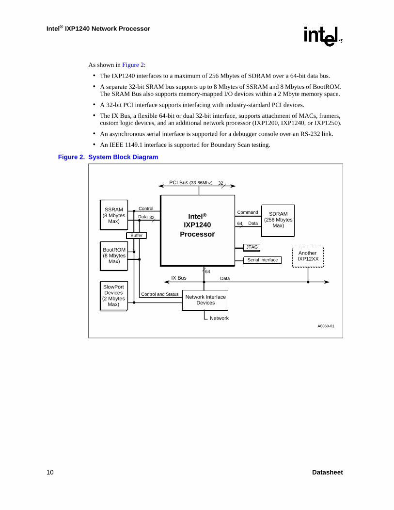
As shown in Figure 2:
• The IXP1240 interfaces to a maximum of 256 Mbytes of SDRAM over a 64-bit data bus.
• A separate 32-bit SRAM bus supports up to 8 Mbytes of SSRAM and 8 Mbytes of BootROM. The SRAM Bus also supports memory-mapped I/O devices within a 2 Mbyte memory space.
• A 32-bit PCI interface supports interfacing with industry-standard PCI devices.
• The IX Bus, a flexible 64-bit or dual 32-bit interface, supports attachment of MACs, framers, custom logic devices, and an additional network processor (IXP1200, IXP1240, or IXP1250).
• An asynchronous serial interface is supported for a debugger console over an RS-232 link.
• An IEEE 1149.1 interface is supported for Boundary Scan testing.
Figure 2. System Block Diagram
A8869-01
SSRAM(8 Mbytes
Max)
BootROM(8 Mbytes
Max)
Network InterfaceDevices
Control and Status
PCI Bus (33-66Mhz)
SlowPortDevices
(2 MbytesMax)
SDRAM(256 Mbytes
Max)
32
32
64
Command
Data
Data
Control
IX Bus 64
Data
Network
Another IXP12XX
Buffer
Serial Interface
JTAG
Intel®IXP1240
Processor
10 Datasheet
Intel® IXP1240 Network Processor
2.0 Functional Units
2.1 Conventions
• In all signal descriptions, an active low signal is indicated by the _L in the signal name.
• In this and related IXP1240 documents, a word is equal to 16 bits, a longword is equal to 32 bits, and a quadword is equal to 64 bits. StrongARM* processor documents and the ARM* V4.0 Architecture Reference typically refer to a word as being equal to 32 bits, and a halfword as being equal to 16 bits.
2.2 StrongARM* Core
The StrongARM* core is the same industry standard 32-bit RISC processor as used in the Intel® StrongARM* SA-1100. It is compatible with the StrongARM* processor family currently used in applications such as network computers, PDAs, palmtop computers and portable telephones. The differentiating feature of the StrongARM* processor is that it provides very high performance in a low-power, compact design. This makes it feasible to combine it with a collection of other dedicated execution units on the same silicon die.
The StrongARM* core processor and six RISC Microengines provide the processing power required to forward greater than 3 million Ethernet packets per second through the IXP1240. A multi-IXP1200 Network Processor Family system scales linearly so that a system comprised of eight IXP1200s can process over 24 million packets per second.
The designer can partition his/her application by allocating Microengines, threads, and StrongARM* tasks. If necessary, multiple IXP1200 Network Processor Family devices can be used to aggregate CPU MIPs, increase data bandwidth, increase port fanout and density, or some combination of all three metrics.
The StrongARM* core operates at a frequency determined by programming the Phase-Locked Loop Configuration register (PLL_CFG) and the maximum rated operating frequency of the IXP1240 device selected. The IXP1240 is currently available with an Fcore operating frequency of 166, 200, or 232 MHz.
2.3 Microengines
Six 32-bit, multithreaded RISC Microengines perform data movement and processing without assistance from the StrongARM* core. Each Microengine has four independent program counters, zero overhead context switching and hardware semaphores from other hardware units to ensure that each Microengine can be fully utilized. A Microengine’s powerful ALU and shifter perform both ALU and shift operations in a single cycle. The instruction set was specifically designed for networking and communications applications that require bit, byte, word and longword operations to forward data quickly and efficiently. Each Microengine contains a large amount of local memory and registers: 8 Kbytes organized as 2048 by 32 bits of high-speed RAM Control Store for program execution, 128 32-bit General Purpose Registers, and 128 32-bit transfer registers to service the SRAM and SDRAM Units.
The Microengines operate at the core clock frequency (Fcore).
Datasheet 11
Intel® IXP1240 Network Processor
2.4 FBI Unit and the IX Bus
The FBI Unit is responsible for servicing fast peripherals, such as MAC-layer devices, on the IX Bus. This includes moving data to and from the IXP1240 Receive and Transmit FIFOs.
The IX Bus provides a 4.4 Gbps interface to peripheral devices. The IX Bus was specifically designed to provide a simple and efficient interface. The IX Bus can be configured as either a 64-bit bidirectional bus or as two 32-bit unidirectional buses. The maximum operating frequency of the IX Bus is 104 MHz.
Two IXP1200 Network Processor Family devices can be placed on a single IX Bus in shared IX Bus mode. This option is supported only in 64-bit bidirectional mode.
The FBI Unit contains the Transmit and Receive FIFO elements, control and status registers (CSRs), a 4 Kbyte Scratchpad RAM, and a Hash Unit for generating 48- and 64-bit hash keys. It also contains the drivers and receivers for the IX Bus.
The IX Bus consists of 64 data pins, 23 control pins, and a clock input pin. A sideband bus operating in parallel to the IX Bus, called the Ready Bus, consists of eight additional data pins and five control pins.
The Ready Bus is synchronous to the IX Bus clock, but operation is controlled by a programmable hardware sequencer. Ready Bus cycles are separate and distinct from IX Bus cycles. Up to twelve sequencer commands are loaded at chip initialization time, and run in a continuous loop. The commands can consist of sampling FIFO status for the IX Bus devices, sending Flow Control messages to MAC devices, and reads/writes to other IXP1200 Network Processor Family devices as required by the application design. Refer to the IXP1200 Network Processor Family Hardware Reference Manual for specific details on using the Ready Bus.
2.4.1 IX Bus Access Behavior
There are two basic modes of IX Bus operation. This is a configuration option only and is not intended to be used “on the fly” to switch between modes.
• 64-Bit Bidirectional Mode
The entire 64-bit data path FDAT[63:0] is used for reads or writes to IX Bus devices. The IXP1240 always drives and receives all 64 bits of the IX Bus in this mode. Valid bytes are indicated on the FBE_L[7:0] signals driven by the IXP1240 during writes and by the IX Bus slave device on reads.
• 32-Bit Unidirectional Mode
The IX Bus is split into independent 32-bit transmit and 32-bit receive data paths. Transmit data is driven on FDAT[63:32] and receive data is input on FDAT[31:0]. In this mode, the transmit path is always driven. The receive path is an input during receive cycles and driven by the IXP1240 during device reset cycles or during prolonged idle time on the bus. Valid bytes are identified for the transmit path by the FBE_L[7:4] signals. Valid bytes are identified for the receive path by the FBE_L[3:0] signals.
Each basic mode has two additional modes depending on the number of IX Bus devices and ports being used: 1-2 MAC mode for one or two slave devices, and 3+ MAC mode when using three to seven slave devices. Bus timing and the functions of the IX Bus signals are slightly different in each mode. These functional definitions per IX Bus mode are listed in Section 3.6 and Section 3.7.
12 Datasheet
Intel® IXP1240 Network Processor
In addition, a shared IX Bus mode is supported in 64-bit bidirectional mode. Refer to the list at the bottom of Table 26 for the signals that the IX Bus masters must drive and IX Bus slaves must tri-state.
The IX Bus and Intel devices using the IX Bus, such as the 21440 and IXF1002, observe a pipelined bus protocol. When receive transfers are terminated early, the pipeline continues to cause several extra bus cycles depending on when the EOP signal was asserted. Data is a “don't care” for these trailing bus cycles, except in the case of a status transfer where the IX Bus burst includes a possible status transfer if the device were programmed to support it. Slave devices must drive valid logic levels on the FDAT data pins during these cycles.
The tables below show the number of total IX Bus data cycles that will occur for a burst with EOP asserted at specific clocks for 64-bit and 32-bit IX Bus modes. In each case, the tables show IX Bus cycles with and without the optional status transfer cycle. Refer to the IX Bus Protocol Timing diagrams (Figure 21 through Figure 54) when interpreting these tables.
Table 1. 64-bit IX Bus Receive Remainder Cycles, No Status Transfer
EOP signaled on this cycle: 1 2 3 4 5 6 7 8
# of bus cycles in burst: 5 6 7 8 8 8 8 8
# of Don’t Care cycles: 4 4 4 4 3 2 1 0
Table 2. 64-bit IX Bus Receive Remainder Cycles, with Status Transfer
EOP signaled on this cycle: 1 2 3 4 5 6 7 8
# of bus cycles in burst: 5 6 7 8 8 8 8 8
Status transfer 1 1 1 1 1 1 1 Note 1
# of Don’t Care cycles: 3 3 3 3 2 1 0 0
NOTE:1. Status transfer occurs on a subsequent IX Bus status cycle.
Table 3. 32-bit IX Bus Receive Remainder Cycles, No Status Transfer
EOP signaled on this cycle: 1 2 3 4 5 6 7 8 9 10 11 12 13 14 15 16
# of bus cycles in burst: 5 6 7 8 9 10 11 12 13 14 15 16 16 16 16 16
# of Don’t Care cycles: 4 4 4 4 4 4 4 4 4 4 4 4 3 2 1 0
Table 4. 32-bit IX Bus Receive Remainder Cycles, with Status Transfer
EOP signaled on this cycle: 1 2 3 4 5 6 7 8 9 10 11 12 13 14 15 16
# of bus cycles in burst: 5 6 7 8 9 10 11 12 13 14 15 16 16 16 16 16
Datasheet 13

Intel® IXP1240 Network Processor
In both 32-bit and 64-bit modes, all of the associated FBE_L signals (FBE_L[7:4] in 32-bit mode and FBE_L[7:0] for 64-bit mode) are driven low on a transmit. The last bus transfer, identified by the assertion of EOP in 64-bit mode or by EOP32 in 32-bit mode, indicates the number of valid bytes of this last transfer by driving only the valid FBE_L signals.
Similarly for receive cycles, in both 32-bit and 64-bit modes, all associated FBE_L signals must be driven low by the peripheral or MAC device. The FBE_L signals must identify the number of valid bytes on the last transfer driven with EOP. The IXP1240 uses this information to update the RCV_CTL register’s Valid Bytes field. Driving fewer than the four or eight FBE_Ls, except for the last transfer with EOP, may cause undefined behavior.
2.4.1.1 Reset and Idle Bus Considerations
While the IXP1240 is in reset, or when the IX Bus is idle for at least 4 FCLK cycles and no bus requests are pending, the IXP1240 drives the pins listed below. This is done so that the bus is not left in a high-Z state for a prolonged period of time. This allows the designer to avoid the use of keeper resistors on the pins to maintain valid levels.
FDAT[63:0]FBE_L[7:0]FPS[2:0]TXASISRDYBUS[7:0]RDYCTL_L[3:0]RDYCTL_L[4]EOPSOPEOP32SOP32RXFAIL
In shared IX Bus mode, pullups should be used on PORTCTL_L[3:0], FPS[2:0], and TXASIS to maintain valid logic levels during bus exchanges.
In configurations where two IXP1240s are in Shared IX Bus Mode, the IXP1240s must be reset synchronously, preferably with the same signal driving RESET_IN_L. During reset, the IXP1240s drive the pins listed above to identical logic states thereby avoiding logic state contention. If the two devices are not reset synchronously, bus contention could result if one of the devices is held in reset while the alternate device assumes the role of initial IX Bus owner and begins driving transactions. This would result in obvious bus malfunction, and over time could affect device reliability due to resulting high current conditions in the device.
Status transfer
32-bit status 1 1 1 1 1 1 1 1 1 1 1 1 1 1 1 Note1
64-bit status 2 2 2 2 2 2 2 2 2 2 2 2 2 2 2
# of Don’t Care cycles: 3 3 3 3 3 3 3 3 3 3 3 3 2 1 0 0
NOTE:1. Status transfer occurs on one or two subsequent IX Bus cycles.
Table 4. 32-bit IX Bus Receive Remainder Cycles, with Status Transfer
14 Datasheet
Intel® IXP1240 Network Processor
2.5 SDRAM and SRAM Units
The IXP1240 supports two high performance memory units. The SRAM Unit provides fast memory that can be used to store look-up tables. The SDRAM Unit provides lower cost memory for forwarding information and transmit queues. Both units contain features that improve memory bandwidth utilization.
2.5.1 SDRAM Unit
The IXP1240 provides an SDRAM Unit to access low cost, high bandwidth memory for mass data storage. The StrongARM* core address space allows up to 256 Mbytes of SDRAM to be addressed. The SDRAM interface operates at half the core frequency (0.5*Fcore), providing a peak bandwidth of 928 Mbytes per second at 232 MHz.
Bus cycles are generated by requests from the PCI Unit including PCI DMA cycles, the StrongARM* core, and the Microengines.
The SDRAM is operated by commands that are loaded into command queues within the unit. The SDRAM Unit decodes the command, reads or writes the data, then deletes the command from the head of the queue. The read and write sources may be SDRAM memory locations, transfer registers, or the Transmit and Receive FIFOs in the FBI Unit. Refer to the IXP1200 Network Processor Family Hardware Reference Manual for details on how these requests are queued, prioritized, and serviced by the SDRAM Unit.
SDRAM should have an access time (tac) of 6 ns or less (CAS latency = 2), PC100 compatible.
Datasheet 15

Intel® IXP1240 Network Processor
Figure 3 details the major components of the SDRAM Unit.
The SDRAM Bus consists of 15 row/column address bits, 64 data bits, RAS_L, CAS_L, write enable, DQM control, and a synchronous output clock running at one-half the IXP1240 core frequency (0.5*Fcore).
The PCI, Microengines, and StrongARM* core require single byte, word, and longword write capabilities. The SDRAM Unit supports this using a read-modify-write technique. As data is written from the PCI or StrongARM* core to SDRAM, a quadword is read from SDRAM. The IXP1240 then updates only the bytes that were enabled and writes the entire quadword of data back to SDRAM memory. (Note that the bytes do not have to be consecutive.) These three steps are performed automatically.
2.5.2 SDRAM Bus Access Behavior
• The number of quadwords transferred by the SDRAM Unit is determined by the requesting interface (StrongARM* core, Microengine, or PCI). The SDRAM Unit may reorder SDRAM accesses for best performance.
• Accesses are always quadword (64-bit) cycles on the SDRAM Bus.
• Accesses from the StrongARM* core.
— Byte, word, and longword accesses generated from the StrongARM* core result in Read-Modify-Write cycles to SDRAM space.
— Consecutive longword writes over the AMBA Bus to the same quadword address are buffered and aggregated into quadword writes to SDRAM.
Figure 3. SDRAM Unit Block Diagram
A8907-01
AMBA[31:0]
(fromStrongARM *Core)
MicroengineCommands &Addresses
Microengine Data [63:0]
SDRAMup to
256 MB
SDRAMPin
Interface
CommandDecoder
& Address Generator
Service Priority(Arbitration)
Machine & Registers
AMBA BusInterface
Logic
AMBA AddressRd/Wr Queue
PCI AddressRD/Wr Queue
Microengine Address& Command Queues(High Priority, Even,
Odd & Order)
Memory/AMBA Data
FIFOAddr[14:0]
Data[63:0]
WE_L,RAS_LCAS_L, DQM
addr
data
SDCLK
PCI Commandsand Addresses
* Other names and brands may be claimed as the property of others.** ARM architecture compatible
16 Datasheet
Intel® IXP1240 Network Processor
— Read accesses using the Prefetch Memory address space allow the SDRAM Unit to prefetch quadword data to be supplied to the AMBA Bus using 32-bit burst cycles.
• Accesses from the Microengines.
— The sdram microinstruction defines the number of 64-bit accesses to make, with up to 16 quadwords with one instruction.
— Only quadword accesses are supported. Less than 8 bytes can be written when using the byte mask within an instruction, but result in Read-Modify-Write cycles.
2.5.3 SDRAM Cyclic Redundancy Checking (CRC)
SDRAM Cyclic Redundancy Checking (CRC) is used to protect blocks of data called Frames. Using this technique, the transmitter appends an extra n-bit sequence (called a Frame Check Sequence or FCS) to every frame. The FCS holds redundant information about the frame that helps the transmitter detect errors in the frame.
The CRC is one of the most used techniques for error detection in data communications. The technique combines three advantages:
• Extreme error detection capabilities
• Minimal overhead
• Ease of implementation
CRC generation is performed in the SDRAM unit and is controlled by Microengine instructions. All CRC checking and appending is also handled by the Microengines.
The CRC types supported are described in Table 5.
Table 5. SDRAM CRC Types
CRC Type Polynomial Application Bit Order
CRC-32 X 32 +X 26 +X 23 +X 22 +X 16 +X 12 +X 11 +X 10 +X 8 +X 7 +X 5 +X 4 +X2 +X+1
ATM AAL5
Ethernet
MSB first
LSB first
CRC-16 X 16 +X 12 +X 5 +1HDLC
Frame Relay
LSB first
LSB first
CRC-10 x 10 +x 9 +x 5 +x 4 +x+1 ATM OAMMSB first,
LW (or LW +1)
Datasheet 17

Intel® IXP1240 Network Processor
2.5.4 SDRAM Configurations
2.5.5 SRAM Unit
The IXP1240 provides an SRAM Unit for very high bandwidth memory for storage of lookup tables and other data for the packet processing Microengines. The SRAM Unit controls the SRAM (up to 8 Mbytes), BootROM (up to 8 Mbytes) for booting, and 2 Mbytes of SlowPort address space for peripheral device access. The I/O signal timing is determined by internal address decodes and configuration registers for the BootROM and SlowPort address regions. The SRAM Unit includes an 8 entry Push/Pop register list for fast queue operations, bit test, set and clear instructions for atomic bit operations, and an 8 entry CAM for Read Locks.
The SRAM interface operates at one-half the IXP1240 core frequency (0.5 * Fcore).
The SRAM Unit supports both Pipelined Burst Double Cycle Deselect (DCD) and Flowthru SRAM types. Other SSRAM devices, including single cycle deselect, are not supported. The bus is also used to attach BootROM and can be used to interface other peripheral devices such as custom interface logic or MAC management ports. The SRAM interface provides three separate timing domains for the three device types: SRAM, BootROM, and Peripheral (also referred to as SlowPort access).
BootROM devices may be either 32 bits or 16 bits in width. This is determined by GPIO[3] during reset. When 16-bit BootROM devices are used, the maximum BootROM address space is reduced from 8 Mbytes to 4 Mbytes.
Figure 4 details the major components of the SRAM Unit.
Table 6. SDRAM Configurations
Total Memory
Number of Chips
Size DRAM
Configuration (per bank)
InternalBanks Bank Bits RAS Bits CAS Bits
8 Mbytes 4 16 Mbit 512 K x 16-bit 2 1 11 8
16 Mbytes 8 16 Mbit 1 M x 8-bit 2 1 11 9
32 Mbytes 4 64 Mbit 2 M x 16-bit 2 1 13 8
64 Mbytes 8 64 Mbit 4 M x 8-bit 2 1 13 9
32 Mbytes 4 64 Mbit 1 M x 16-bit 4 2 12 8
64 Mbytes 8 64 Mbit 2 M x 8-bit 4 2 12 9
64 Mbytes 4 128 Mbit 2 M x 16-bit 4 2 12 9
128 Mbytes 8 128 Mbit 4 M x 8-bit 4 2 12 10
128 Mbytes 4 256 Mbit 4 M x 16-bit 4 2 13 9
256 Mbytes 8 256 Mbit 8 M x 8-bit 4 2 13 10
18 Datasheet

Intel® IXP1240 Network Processor
The SRAM Bus consists of 19 address bits, 32 data bits, 4 chip enable bits, 8 buffer and read/write control signals, a synchronous output clock (SCLK) running at one-half the IXP1240 core frequency, and a synchronous input clock (NA/SACLK). When using Flowthru SRAM types, it is recommended to route the SCLK signal from the SRAMs back to the NA/SACLK input. Routing this trace identically to the DQ data signals will skew the NA/SACLK slightly to track the return data trace propagation delay. When using Pipelined/DCD SRAMs, the NA/SACLK input is not used and may be held inactive with a pulldown to GND to save power.
The SRAM Unit receives memory requests from seven sources: the StrongARM* core and each of the six Microengines. Refer to the IXP1200 Network Processor Family Hardware Reference Manual for details on the prioritization and queues provided for servicing these requests.
The IXP1240 supports the use of an optional asynchronous ready input for flexibility in interfacing memory-mapped I/O devices to the SRAM Slowport region. This will allow the I/O device to add wait-states to IXP1240 I/O accesses. This function is supported on the HIGH_EN_L pin. An I/O device must drive HIGH_EN_L with a wired-OR open drain buffer configuration, and only drive the pin when the I/O device is selected.
To use the RDY_L pin function, it must be enabled by setting SRAM_CSR[19]=1. The RDY_L Pause State Value field located in register SRAM_SLOW_CONFIG[23:16] must be programmed with the state value at which you choose to pause the internal wait-state logic. This pause state relates to the other timing parameters programmed into the SRAM_SLOW_CONFIG and SRAM_SLOWPORT_CONFIG register fields. See Figure 73 which illustrates this example. The SCC value is the total number of core clocks for the I/O cycle, and the SRWA, SCEA, SRWD, and SCED values specify the RD/WR and Chip Enable signal assert and deassert times. When the I/O cycles begins, the SCC value is loaded into the internal state counter and is decremented on each
Figure 4. SRAM Unit Block Diagram
A8545-01
AMBA[31:0]
(fromStrongARM*Core)
MicroengineCommands &Addresses
Microengine Data [63:0]
SRAM32KB to
8MBPipelined-
DCD orFlowthru
Buffer
SRAMPin
Interface
CommandDecoder
& Address Generator
Service Priority(Arbitration)
Machine & Registers
AMBA BusInterface
Logic
AMBA AddressRd/Wr Queue
Microengine Address& Command Queues(High Priority, Read,
Readlock Failand Order)
Memory/AMBA Data
FIFOAddr[18:0]
Data[31:0]
RD/WR/ENSignals
addr
data
* Other names and brands may be claimed as the property of others.** ARM architecture compatible
BootROM256KB
to8 MB
PeripheralDevice
(i.e., MACCPU port)
SCLK
Datasheet 19

Intel® IXP1240 Network Processor
core clock tick (twice the SCLK frequency). When the state counter reaches the RDY_L Pause State Value, it will remain in that state until the HIGH_EN_L pin is sampled LOW, allowing the state counter to resume its decrement operation. The HIGH_EN_L must be driven for at least two SCLK periods to be sampled properly by the IXP1240.
The RDY_L Pause State must also occur at a minimum of 5 core clock periods prior to the SRWD state to be recognized. A RDY_L Pause State value of SRWD+5 (Decimal 10, Hexidecimal A) is used in this example.
In this example, 6 additional core clock “wait-states” are inserted. If the RDY_L input is synchronous to SCLK and it meets the specified setup and hold times, the resulting number of wait states will be predictable. However, if the RDY_L input is asynchronous to SCLK, the number of wait-states the IXP1240 inserts could vary by +/- 2 core clock periods.
2.5.5.1 SRAM Types Supported
Pipeline Burst DCD (double cycle deselect) type: tKQmax=4.2 ns, 3.3 V.
Flowthru type: tKQmax= 9 ns, 3.3 V.
Note: Other SSRAM devices, including single cycle deselect, are not supported.
2.5.5.2 SRAM Configurations
2.5.5.3 BootROM Configurations
Table 7. SRAM Configurations
Total Memory Number of Chips(Maximum of 8) Size of SRAM Device Organization
1 Mbytes 8 1 Mbit 32 K x 32-bit
2 Mbytes 8 2 Mbit 64 K x 32-bit
2 Mbytes 8 2 Mbit 128 K x 16-bit
4 Mbytes 8 4 Mbit 128 K x 32-bit
4 Mbytes 8 4 Mbit 256 K x 16-bit
8 Mbytes (maximum) 8 8 Mbit 256 K x 32-bit
Table 8. BootROM x32 Sample Configurations
Total Memory Number of Chips(Maximum of 8) Size of Boot ROM Device Organization
512 Kbytes 2 2 Mbit 128 K x 16-bit
2 Mbytes 8 2 Mbit 128 K x 16-bit
4 Mbytes 8 4 Mbit 256 K x 16-bit
6 Mbytes 6 8 Mbit 512 K x 16-bit
8 Mbytes 8 8 Mbit 512 K x 16-bit
20 Datasheet

Intel® IXP1240 Network Processor
2.5.5.4 SRAM Bus Access Behavior
• The SRAM controller within the IXP1240 will never initiate automatic bursting. Bursting is controlled by the requestor (StrongARM* core or Microengine) depending on the type and number of SRAM accesses needed.
• Accesses are always longword 32-bit cycles on the SRAM Bus.
• The IXP1240 always drives the address for each data cycle. No external address generation or address advance control to SRAM devices is required.
• Accesses from the StrongARM* core:
— Byte, word, and longword accesses generated from the StrongARM* core are supported.
— Bit operations are supported via StrongARM* core accesses to the SRAM Alias Address Space to perform the same operations as a Microengine can accomplish implicitly in a microinstruction (Push, Pop, Bit Test and Set, CAM operations, Lock/Unlock, etc.).
— Bit, byte, and word writes result in Read-Modify-Write cycles.
— Declare memory-mapped I/O as non-cachable to prevent line fill burst cycles, and disable caching and write buffering to ensure I/O device coherency.
— For best performance, use longword accesses to avoid Read-Modify-Write cycles on the SRAM Bus that occur with byte and word accesses.
• Accesses from the Microengines:
— The sram microinstruction defines the number of 32-bit accesses to make, up to 8 longwords with one Microengine command.
— Only bit and longword accesses are supported.
— Bit write accesses result in Read-Modify-Write cycles.
— Unlike the StrongARM* core, the Microengine microinstruction allows you to perform bit operations within the instruction (Push, Pop, Bit Test and Set, CAM operations, Lock/Unlock, etc.).
Table 9. BootROM x16 Sample Configurations
Total Memory Number of Chips(Maximum of 8) Size of Boot ROM Device Organization
256 Kbytes 1 2 Mbit 128 K x 16-bit
512 Kbytes - 4 Mbytes 2 - 8 2 Mbit 128 K x 16-bit
512 Kbytes 1 4 Mbit 256 K x 16-bit
1 Mbytes - 4 Mbytes 2 - 8 4 Mbit 256 K x 16-bit
1 Mbytes 1 8 Mbit 512 K x 16-bit
2Mbytes - 4 Mbytes 2 - 4 8 Mbit 512 K x 16-bit
Datasheet 21

Intel® IXP1240 Network Processor
2.6 PCI Unit
The PCI Unit provides an industry standard 32-bit PCI Bus to interface to PCI peripheral devices such as host processors and MAC devices. The PCI Unit supports operating speeds from DC up to 66 MHz, and supports PCI Local Bus Specification, Revision 2.2. This unit contains:
• Arbitration logic to support up to three PCI Bus masters,
• PCI Intelligent I/O (I2O),
• Two DMA channels, and
• Four 24-bit timers.
Refer to the IXP1200 Network Processor Family Hardware Reference Manual for details on PCI Bus behavior for Target (Slave) and Initiator (Master) modes, configuration and register definitions.
The PCI interface is specified to operate from DC up to 66 MHz. Above 33 MHz operation, two PCI devices are supported only, the IXP1240 and a second PCI device. To increase the number of PCI devices supported or to add connectors to the bus at the higher PCI Bus speeds, a PCI-to-PCI bridge device, such the Intel 21150, 21152, or 21153 is required.
Both PCI Initiator and Target cycles are supported. As a target device, the IXP1240 responds as a Medium Speed device asserting DEVSEL_L two PCI_CLK cycles after FRAME_L is asserted.
2.6.1 PCI Arbitration and Central Function Support
The IXP1240 contains an optional arbiter to support up to three PCI Bus masters. This includes the IXP1240 plus two external PCI Bus master devices. The external masters are supported by two request signals, REQ_L[1:0], and two grant signals GNT_L[1:0].
The IXP1240 can also provide PCI Central Function support. In this configuration, the IXP1240:
• Drives the PCI Reset signal, PCI_RST_L, as an output,
• Monitors the PCI System Error input signal, SERR_L, and
• Provides Bus Parking where the IXP1240 is the default PCI Bus master, and it drives valid logic levels on the PCI A/D, C/BE, and PAR pins during reset and idle PCI Bus conditions.
Two configuration pins, PCI_CFN[1:0], are sampled at the rising edge of RESET_IN_L to determine the PCI configuration (see Table 10).
Table 10. PCI Configuration Options
PCI_CFN[1:0] PCI FUNCTION
00 Central Function and Arbitration disabled.
10 Reserved for future use.
01 Reserved for future use.
11 Central Function and Arbitration enabled.
22 Datasheet

Intel® IXP1240 Network Processor
2.7 Device Reset
The IXP1240 can be reset by the following:
• Hardware Reset via RESET_IN_L pin
• Software Reset by StrongARM* core or by PCI device write to the IXP1200_RESET register
• PCI Reset via the PCI_RST_L pin
• Watchdog Timer expiration
Figure 5 illustrates details of the internal reset function logic.
Datasheet 23

Intel ® IX
P1240 N
etwo
rk Pro
cessor
24 D
atasheet
Fig
ure 5. R
eset Lo
gic
RESET_IN_L
PCI_RST_L
PCI_CFG[0]
RESET_CSR_wr_enasserted when: PCI or Corewrites to the RESET CSR.
watchdog_timer
PCI or StrongARM core writeto the PCI Reset CSR
Internal Signals
Input Pin
!zero cyclenter
ardt timer
PXTAL
(Should be asserted 150msafter power supply is stable)
Core clock
Input Pin
Input/Output Pin
0 = reset in1 = reset out
A8546-01
async set
syncclear
RESET_OUT_Lext_rst
microengine5_rst
sdram_rst
fbi_rst
QD QD
synchro
microengine4_rstmicroengine3_rstmicroengine2_rstmicroengine1_rstmicroengine0_rst
sram_rst
strongarm_rstpci_rst
InternalReset Signals
Coreclock
ueng5reset
ueng4reset
ueng3reset
ueng2reset
ueng1reset
ueng0reset
sramreset
sdramreset
cmdarb
reset
fbireset
extreset
PCIreset
SACorereset
res res
[14:7][28:19]
Output Pin
[0][1][2][3][4][5][15][16][17][29][30][31] [18]
cmd_arb_rst
rst_in_sync
start512cou
Hrese
Core clock
Core clock
[6]
PCIBusresetout
start !zero
140 cyclecounter
Softreset timer

Intel® IXP1240 Network Processor
2.7.1 Hardware Initiated Reset
The IXP1240 provides the RESET_IN_L pin so that an external device can reset the IXP1240. Asserting this pin resets the internal functions and generates an external reset via the RESET_OUT_L pin.
Upon power-up, RESET_IN_L must remain asserted for 150 ms after VDD and VDDX are stable to properly reset the IXP1240 and ensure that the PXTAL clock input and PLL Clock generator are stable.
While RESET_IN_L is asserted, the processor is held reset. When RESET_IN_L is released, the StrongARM* processor begins execution from SRAM address 0 after 512 PXTAL cycles. If RESET_IN_L is asserted while the StrongARM* core is executing, the current instruction terminated abnormally and the on-chip caches, MMU, and write buffer are disabled.
The RESET_OUT_L signal remains asserted until deasserted by the StrongARM* core. The StrongARM* core deasserts the signal by writing bit 15 of the IXP1200_RESET register.
2.7.2 Software Initiated Reset
The StrongARM* core or an external PCI Bus master can reset specific functions in the IXP1240 by writing to the IXP1200_RESET register. In most cases, only the individual Microengines are reset and the external RESET_OUT_L pin will be asserted via this register. The ability to reset the other functions is provided for debugging. The SRAM Unit is always reset when the StrongARM* core is reset. To ensure a proper reset, the StrongARM* core and the SRAM Unit are held in reset for 140 system clock cycles after RESET_IN_L is deasserted. The other functions that can be reset via the IXP1200_RESET register are properly reset when consecutive writes are performed to assert and deassert the reset.
2.7.3 PCI Initiated Reset
The IXP1240 can be reset by an external PCI Bus master when the IXP1240 is not the PCI Central Function and arbiter device (PCI_CFG[1:0] = 00) and PCI_RST_L is an input. The entire IXP1240 is reset during a PCI Initiated Reset. When the IXP1240 is assigned as the PCI Central Function and arbiter device (PCI_CFG[1:0] = 11), the IXP1240 drives PCI_RST_L as an output to the other devices on the PCI Bus.
2.7.4 Watchdog Timer Initiated Reset
The IXP1240 provides a watchdog timer that can reset the StrongARM* core. The StrongARM* core should be programmed to reset the watchdog timer periodically to ensure that the timer does not expire. If the watchdog timer expires, it is assumed the StrongARM* core has ceased executing instructions properly. The reset generated by the Watchdog Timer will reset each of the functions in the IXP1240.
Datasheet 25
Intel® IXP1240 Network Processor
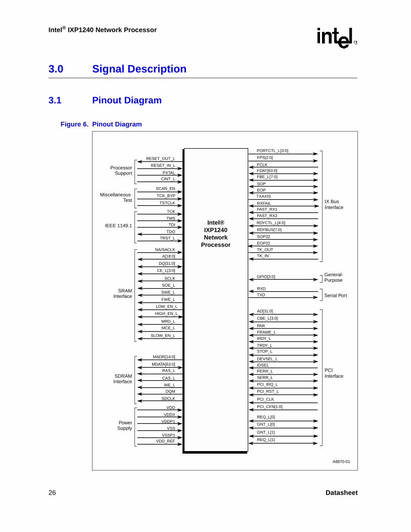
3.0 Signal Description
3.1 Pinout Diagram
Figure 6. Pinout Diagram
A8870-01
Intel®IXP1240Network
Processor
TCK_BYP
SCAN_EN
TSTCLK
CINT_L
PXTALProcessor
Support
TCK
TRST_L
TDO
TDI
TMS
IEEE 1149.1
A[18:0]
DQ[31:0]
CE_L[3:0]
FCLK
MRD_L
MCE_L
LOW_EN_L
FWE_L
SWE_L
SOE_L
SCLK
NA/SACLK
HIGH_EN_L
SLOW_EN_L
SRAMInterface
MADR[14:0]
MDATA[63:0]
SDCLK
DQM
WE_L
CAS_L
RAS_LSDRAMInterface
PORTCTL_L[3:0]
FPS[2:0]
FBE_L[7:0]
RXD
FDAT[63:0]
TXAXIS
EOP
SOP
EOP32
TK_OUT
TK_IN
SOP32
RDYBUS[7:0]
FAST_RX1
FAST_RX2
IX BusInterface
FRAME_L
PAR
TXD
IRDY_L
PERR_L
DEVSEL_L
TRDY_L
SERR_L
RXFAIL
STOP_L
IDSEL
VDD_REF
Serial Port
General-Purpose
AD[31:0]
CBE_L[3:0]
RESET_OUT_L
PCI_IRQ_L
RESET_IN_L
VSSP1
PCI_RST_L
PCI_CLK
PCI_CFN[1:0]
REQ_L[0]
GNT_L[0]
GNT_L[1]
REQ_L[1]
PCIInterface
PowerSupply
VDD
VDDX
VDDP1
VSS
Miscellaneous Test
RDYCTL_L[4:0]
GPIO[3:0]
26 Datasheet
Intel® IXP1240 Network Processor
3.2 Pin Type Legend
The IXP1240 signals are categorized into one of several groups: Processor Support, Miscellaneous/Test, IEEE 1149.1, SRAM Interface, SDRAM Interface, IX Bus Interface, General Purpose, Serial Port, and PCI Interface.
Table 11 defines the signal type abbreviations used in the Pin Description section.
Table 11. Signal Type Abbreviations
Signal Type Description
I Standard input only. There are three types of inputs (I1,I2, and I3) for the IXP1240. Refer to Table 35 and Table 36 for more information.
O Standard output only. There are 5 types of outputs (O1,O2,O3,O4, O5) for the IXP1240. Refer to Table 35 and Table 36 for more information.
TS Tri-state output.
STS
Sustained tri-state. Active low signal owned and driven by one and only one agent at a time. The agent that drives this pin low must drive it high for at least one clock before letting it float. A new agent cannot start driving this signal any sooner than one clock after the previous owner tri-states it. A pullup is required to sustain the inactive state until another agent drives it, and it must be provided by the central resource (that is, on a PC board).
P Power supply.
ODStandard open drain allows multiple devices to share as a wire-OR. A pullup is required to sustain the inactive state until another agent drives it, and it must be provided by the central resource.
Datasheet 27

Intel® IXP1240 Network Processor
3.3 Pin Description, Grouped by Function
3.3.1 Processor Support Pins
Table 12. Processor Support Pins
Processor Support Signal Names Pin # Type Total Pin Descriptions
PXTAL B4 I1 1 Input connection for system oscillator. Typically 3.6864 MHz. Drives internal PLL clock generator.
CINT_L Y28 I1 1 Level-sensitive interrupt input to the StrongARM* core.
RESET_OUT_L A5 O4 1
IXP1240 System Reset Output. Asserted when:
• RESET_IN_L is asserted.
• PCI Central Function and arbiter disabled (PCI_CFN[1:0]=00) and PCI_RST_L is asserted.
• A soft reset is initiated.
• The Watchdog Timer expires.
To deassert, write register IXP1200_RESET bit 15.
RESET_IN_L C6 I1 1
IXP1240 System Reset Input. If asserted, the IXP1240 will reset and will assert RESET_OUT_L. If PCI Central Function and arbiter enabled (PCI_CFN[1:0]=11), PCI_RST_L output will also be asserted.
Totals: 4
28 Datasheet

Intel® IXP1240 Network Processor
3.3.2 SRAM Interface Pins
Table 13. SRAM Interface Pins
SRAM Interface Signal Names Pin # Type Total Pin Descriptions
A[18:0]
[18][17][16][15][14][13][12][11][10]
[9][8][7][6][5][4][3][2][1][0]
A28B28D27E28D30D31E29F28E30E31F29F30F31G29H28G30G31H29J28
O4 19 Address outputs
DQ[31:0]
[31][30][29][28][27][26][25][24][23][22][21][20][19][18][17][16][15][14][13][12][11][10]
[9][8][7][6][5][4][3][2][1][0]
H30J30J31K29L28K30K31L29M28L30L31M29N28M30M31N29N30N31P29R28P30R29R30R31T28T29T30T31U29U28V30V29
I1/O4 32 32 Bidirectional data signals
Datasheet 29

Intel® IXP1240 Network Processor
CE_L[3:0]
[3][2][1][0]
A26B26C26A27
O4 4 SRAM Bus chip enable outputs. Internally decoded from SRAM address. Valid during SRAM and BootROM accesses.
SCLK W31 O3 1 SRAM clock output - Frequency is one half the speed of the core clock (½ * Fcore).
NA/SACLK B24 I1 1
SRAM clock input, used to compensate for skew in data path when using Flowthru SRAMs. Must be connected to SCLK output when using Flowthru devices. Not used with Pipelined devices and should be pulled low.
SOE_L W30 O4 1 SRAM output enable.
SWE_L Y30 O4 1 SRAM write enable.
FWE_L W28 O4 1 Asynchronous interface write enable (BootROM or MAC devices).
LOW_EN_L D26 O4 1Low order SRAM bank enable and buffer direction select for slow interface. When used as the buffer direction select:
0 = write and 1 = read.
HIGH_EN_L C27 I1/O4 1
High-order SRAM bank enable output and Flash PROM/BootROM read enable or asynchronous Ready input from I/O devices. The pin function is determined by programming SRAM_CSR[19] =1, which enables RDY_L or SRAM_CSR[19] =0, which enables the HIGH_EN_L function.
When using the RDY_L function, I/O devices must drive this signal using a wired-OR configuration, which requires a pullup resistor on this pin. Note that this pin is driven as an output until SRAM_CSR[19] is set.
SLOW_EN_L Y29 O4 1 Slow device enable: 0 = Slow device (BootROM or SlowPort), 1=SRAM.
MCE_L W29 O4 1 Slow asynchronous interface chip enable output.
MRD_L Y31 O4 1 Slow asynchronous interface read enable output.
Totals: 65
Table 13. SRAM Interface Pins (Continued)
SRAM Interface Signal Names Pin # Type Total Pin Descriptions
30 Datasheet
Intel® IXP1240 Network Processor
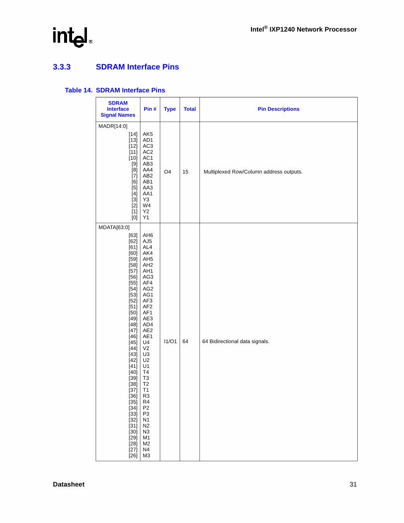
3.3.3 SDRAM Interface Pins
Table 14. SDRAM Interface Pins
SDRAM Interface
Signal NamesPin # Type Total Pin Descriptions
MADR[14:0]
[14][13][12][11][10]
[9][8][7][6][5][4][3][2][1][0]
AK5AD1AC3AC2AC1AB3AA4AB2AB1AA3AA1Y3W4Y2Y1
O4 15 Multiplexed Row/Column address outputs.
MDATA[63:0]
[63][62][61][60][59][58][57][56][55][54][53][52][51][50][49][48][47][46][45][44][43][42][41][40][39][38][37][36][35][34][33][32][31][30][29][28][27][26]
AH6AJ5AL4AK4AH5AH2AH1AG3AF4AG2AG1AF3AF2AF1AE3AD4AE2AE1U4V2U3U2U1T4T3T2T1R3R4P2P3N1N2N3M1M2N4M3
I1/O1 64 64 Bidirectional data signals.
Datasheet 31

Intel® IXP1240 Network Processor
[25][24][23][22][21][20][19][18][17][16][15][14][13][12][11][10]
[9][8][7][6][5][4][3][2][1][0]
L1L2M4L3K1K3J1J2J3H1H2J4H3G1G2H4G3F1F2F3E1E2F4E3D1D2
RAS_L W2 O4 1Row Address Select output.
Precharge cycle indicated if asserted with WE_L.
CAS_L W3 O4 1 Column Address Select output.
WE_L W1 O4 1 Write Enable output.
DQM V3 O4 1SDRAM data control output. SDRAMs use this signal to enable their data buffers to drive MDATA[63:0] on reads, or enable the SDRAM to accept input data from MDATA[63:0] for writes.
SDCLK AD2 O3 1 SDRAM Clock output. Frequency is one half the speed of the core clock (½ * Fcore).
Totals: 84
Table 14. SDRAM Interface Pins (Continued)
SDRAM Interface
Signal NamesPin # Type Total Pin Descriptions
32 Datasheet

Intel® IXP1240 Network Processor
3.3.4 IX Bus Interface Pins
Table 15. IX Bus Interface Pins
IX Bus Signal Names Pin # Type Total Pin Descriptions
FCLK AB30 I3 1 IX Bus Clock input. All IX Bus transfers are synchronized to this clock. Typical operating frequency 33 MHz - 104 MHz.
PORTCTL_L[3:0]
[3][2][1][0]
AC30AC31AB29AA28
O1/TS 4
Port Control outputs. Used to select the transmit and/or receive mode for IX Bus devices, typically MAC devices.
In 64-bit bidirectional IX Bus mode, this is a 4-bit bus used to indicate transmit or receive commands and device selects.
In 32-bit unidirectional IX Bus mode, bits [1:0] are used to select the receive device and bits [3:2] are used to select the transmit device.
In a shared IX Bus system, these pins will be tri-stated when passing ownership of the IX Bus.
FPS[2:0]
[2][1][0]
AC29AD31AD30
O4/TS 3
MAC Port Select outputs.
In 32-bit and 64-bit modes, these pins select one of eight MAC receive ports from the selected MAC device. See IX Bus control signal decode tables.
In a shared IX Bus system, these pins will be tri-stated when passing ownership of the IX Bus.
FDAT[63:0]
[63][62][61][60][59][58][57][56][55][54][53][52][51][50][49][48][47][46][45][44][43][42][41][40][39][38][37][36][35][34][33][32][31]
AC28AD29AE31AE30AF31AF30AF29AG31AG30AF28AG29AH31AH30AH27AK28AL28AJ27AH26AK27AL27AJ26AK26AL26AJ25AH24AK25AL25AJ24AH23AK24AL24AJ23AK23
I2/O5/TS
64
IX Bus Data.
One 64-bit bus in bidirectional IX Bus mode.
Two 32-bit buses in unidirectional IX Bus mode where bits [63:32] are used for Transmit Data output and [31:0] are used for Receive Data input.
In a shared IX Bus system, these pins will be tri-stated when passing ownership of the IX Bus.
Datasheet 33

Intel® IXP1240 Network Processor
[30][29][28][27][26][25][24][23][22][21][20][19][18][17][16][15][14][13][12][11][10]
[9][8][7][6][5][4][3][2][1][0]
AL23AJ22AH21AK22AL22AJ21AH20AK21AL21AJ20AH19AK20AL20AJ19AK19AL19AJ18AH17AK18AJ17AK17AL17AH16AJ16AK16AL16AJ15AH15AK14AJ14AL13
FBE_L[7:0]
[7][6][5][4][3][2][1][0]
AK13AJ13AL12AK12AH13AJ12AL11AK11
I2/O5/TS
8
Bidirectional Byte Enables.
64-bit bidirectional IX Bus mode. Bits [7:0] indicate transmit and receive valid bytes on FDAT[63:0].
32-bit unidirectional IX Bus mode. Bits [7:4] are used to indicate valid transmit bytes on FDAT[63:32] and bits [3:0] are used to indicate valid receive bytes on FDAT[31:0].
In a shared IX Bus system, these pins will be tri-stated when passing ownership of the IX Bus.
TXASIS AL10 O4/TS 1
Transmit As Is/Transmit Error output.
TXASIS states are output according to values programmed in the TFIFO control field. TXASIS value driven coincident with SOP/SOP_TX signal.
In a shared IX Bus system, these pins will be tri-stated when passing ownership of the IX Bus.
RXFAIL AK10 I1/O1/TS 1
Receive Packet Failure. As input, asserted by a MAC device if a packet was received with errors. Mimics the behavior of EOP to terminate an IX Bus cycle.
As output, driven when no receive cycle in-progress.
In a shared IX Bus system, these pins will be tri-stated when passing ownership of the IX Bus.
FAST_RX1 AH11 I1 1 Ready Input from Fast Port 0 (i.e., Gigabit port). Pulldown through 10 KOhms to VSS if not used.
FAST_RX2 AJ10 I1 1 Ready Input from Fast Port 1 (i.e., Gigabit port). Pulldown through 10 KOhms to VSS if not used.
Table 15. IX Bus Interface Pins (Continued)
IX Bus Signal Names Pin # Type Total Pin Descriptions
34 Datasheet

Intel® IXP1240 Network Processor
RDYCTL_L[4] AK6 I1/O4/TS 1
In 64-bit Bidirectional IX Bus Mode:
• 1-2 MAC mode: Used as an active low flow control enable for MAC 1 (GPIO[0] used as a flow control enable for MAC 0).
• 3+ MAC mode: Used in conjunction with RDYCTL_L[3:0].
• In a shared IX Bus system the IXP1240 Ready Bus Master drives this pin. IXP1240 Ready Bus slave devices snoop this pin.
In 32-bit Unidirectional Mode:
• 1-2 MAC mode: Used as an active low flow control enable for MAC 1. GPIO[0] is used as a flow control enable for MAC 0.
• 3+ MAC mode: Used as an active low enable for an external decoder for the PORTCTL[1:0] signals.
RDYCTL_L[3:0]
[3][2][1][0]
AL6AJ7AH8AK7
I1/O4/TS
4
Bidirectional Ready Control signals.
In 64-bit Bidirectional IX Bus Mode:
• 1-2 MAC mode: Bits [3:0] are used to enable the transmit or receive FIFO Ready Flags.
• 3+ MAC mode: The transmit and receive FIFO Ready, the flow control, and inter-processor communication enables are decoded from RDYCTL_L[4:0].
• In a shared IX Bus system the IXP1240 Ready Bus Master drives this bus. IXP1240 Ready Bus slave devices snoop these pins as inputs.
In 32-bit Unidirectional Mode:
• 1-2 MAC mode: Bits [3:0] are used to enable the transmit or receive FIFO Ready Flags.
• 3+ MAC mode: The transmit and receive FIFO ready and flow control enables are decoded from RDYCTL_L[3:0].
RDYBUS[7:0]
[7][6][5][4][3][2][1][0]
AL9AK9AJ9AL8AK8AH9AJ8AL7
I1/O4 8
8-Bit Bidirectional Ready Bus data.
• Inputs the Transmit and Receive Ready Flags from IX Bus devices.
• Outputs flow control data to IX Bus devices.
• Data bus for interprocessor communications.
SOP AH12 I1/O4/TS
1
Start of Packet indication.
• Receive Start of Packet Input in 32-bit unidirectional IX Bus mode.
• Input/Output in 64-bit bidirectional IX Bus mode. Is Receive Start of Packet input during receive cycles.
• In a shared IX Bus system, this pin will be tri-stated when passing ownership of the IX Bus.
EOP AJ11 I1/O4/TS
1
End of Packet Indication.
• Receive End of Packet Input in 32-bit unidirectional IX Bus mode.
• Input/Output in 64-bit bidirectional IX Bus mode. EOP is Transmit End of Packet output according to values programmed in the TFIFO control field. Is Receive End of Packet input during receive cycles.
• In a shared IX Bus system, this pin will be tri-stated when passing ownership of the IX Bus.
Table 15. IX Bus Interface Pins (Continued)
IX Bus Signal Names Pin # Type Total Pin Descriptions
Datasheet 35
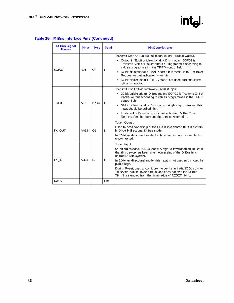
Intel® IXP1240 Network Processor
SOP32 AJ6 O4 1
Transmit Start Of Packet Indication/Token Request Output.
• Output in 32-bit unidirectional IX Bus modes. SOP32 is Transmit Start of Packet output during transmit according to values programmed in the TFIFO control field.
• 64-bit bidirectional 3+ MAC shared bus mode, is IX Bus Token Request output indication when high.
• 64-bit bidirectional 1-2 MAC mode, not used and should be left unconnected.
EOP32 AL5 I1/O4 1
Transmit End Of Packet/Token Request Input.
• 32-bit unidirectional IX Bus modes EOP32 is Transmit End of Packet output according to values programmed in the TFIFO control field.
• 64-bit bidirectional IX Bus modes, single-chip operation, this input should be pulled high.
• In shared IX Bus mode, an input indicating IX Bus Token Request Pending from another device when high.
TK_OUT AA29 O1 1
Token Output.
Used to pass ownership of the IX Bus in a shared IX Bus system in 64-bit bidirectional IX Bus mode.
In 32-bit unidirectional mode this bit is unused and should be left unconnected.
TK_IN AB31 I1 1
Token Input.
64-bit bidirectional IX Bus Mode: A high-to-low transition indicates that this device has been given ownership of the IX Bus in a shared IX Bus system.
In 32-bit unidirectional mode, this input is not used and should be pulled high.
During Reset, used to configure the device as initial IX Bus owner. 1= device is initial owner, 0= device does not own the IX Bus. TK_IN is sampled from the rising edge of RESET_IN_L.
Totals: 103
Table 15. IX Bus Interface Pins (Continued)
IX Bus Signal Names Pin # Type Total Pin Descriptions
36 Datasheet

Intel® IXP1240 Network Processor
3.3.5 General Purpose I/Os
3.3.6 Serial Port (UART) Pins
Table 16. General Purpose I/Os
General Purpose I/O
Signal NamesPin # Type Total Pin Descriptions
GPIO[3:1]
[3][2][1]
A25B25D24
I1/O4 3
Bidirectional General Purpose pins.
64-bit Bidirectional IX Bus mode: Accessible by StrongARM* core. Configurable as Input or Output.
32-bit Unidirectional IX Bus mode: Transmit Port Select [2:0] outputs.
GPIO[3] is sampled during reset to determine if a 32-bit or 16-bit BootROM device is used. If low, enable 32-bit BootROM. If high, Enable 16-bit BootROM.
GPIO[0] C25 I1/O4 1
Bidirectional General Purpose I/O pin.
1-2 MAC mode (Uni or Bidirectional mode): Active low Flow Control Enable output for MAC 0.
3+ MAC 64-bit Bidirectional IX Bus mode: Accessible to the StrongARM* core. Configurable as input or output.
3+ MAC 32-bit Unidirectional IX Bus mode: Active high Transmit Port Enable for an external PORTCTL_L[3:2] decoder.
Totals: 4
Table 17. Serial Port (UART) Pins
Serial Port (UART) Signal
NamesPin # Type Total Pin Descriptions
RXD D23 I1 1 UART Receive data.
TXD C24 O1 1 UART Transmit data.
Totals: 2
Datasheet 37
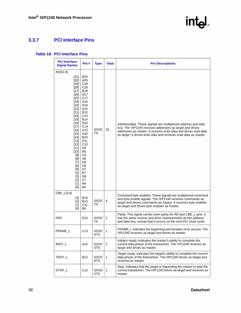
Intel® IXP1240 Network Processor
3.3.7 PCI Interface Pins
Table 18. PCI Interface Pins
PCI Interface Signal Names Pin # Type Total Pin Descriptions
AD[31:0]
[31][30][29][28][27][26][25][24][23][22][21][20][19][18][17][16][15][14][13][12][11][10]
[9][8][7][6][5][4][3][2][1][0]
B20A20C19C18B18D17C17A16D16A15B15C15B14D15C14A13A10B10D11C10A9B9C9A8D9C8A7B7D8C7A6B6
I2/O2/TS
32
Address/data. These signals are multiplexed address and data bus. The IXP1240 receives addresses as target and drives addresses as master. It receives write data and drives read data as target. It drives write data and receives read data as master.
CBE_L[3:0]
[3][2][1][0]
B16B13C11B8
I2/O2/TS
4
Command byte enables. These signals are multiplexed command and byte enable signals. The IXP1240 receives commands as target and drives commands as master. It receives byte enables as target and drives byte enables as master.
PAR D12 I2/O2/TS
1Parity. This signal carries even parity for AD and CBE_L pins. It has the same receive and drive characteristics as the address and data bus, except that it occurs on the next PCI clock cycle.
FRAME_L C13 I2/O2/STS
1 FRAME_L indicates the beginning and duration of an access. The IXP1240 receives as target and drives as master.
IRDY_L A12 I2/O2/STS
1Initiator ready. Indicates the master’s ability to complete the current data phase of the transaction. The IXP1240 receives as target and drives as master.
TRDY_L B12 I2/O2/STS
1Target ready. Indicates the target’s ability to complete the current data phase of the transaction. The IXP1240 drives as target and receives as master.
STOP_L C12 I2/O2/STS
1Stop. Indicates that the target is requesting the master to stop the current transaction. The IXP1240 drives as target and receives as master.
38 Datasheet
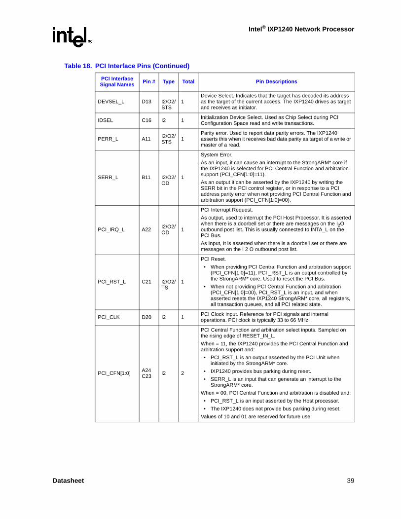
Intel® IXP1240 Network Processor
DEVSEL_L D13 I2/O2/STS
1Device Select. Indicates that the target has decoded its address as the target of the current access. The IXP1240 drives as target and receives as initiator.
IDSEL C16 I2 1 Initialization Device Select. Used as Chip Select during PCI Configuration Space read and write transactions.
PERR_L A11 I2/O2/STS 1
Parity error. Used to report data parity errors. The IXP1240 asserts this when it receives bad data parity as target of a write or master of a read.
SERR_L B11 I2/O2/OD
1
System Error.
As an input, it can cause an interrupt to the StrongARM* core if the IXP1240 is selected for PCI Central Function and arbitration support (PCI_CFN[1:0]=11).
As an output it can be asserted by the IXP1240 by writing the SERR bit in the PCI control register, or in response to a PCI address parity error when not providing PCI Central Function and arbitration support (PCI_CFN[1:0]=00).
PCI_IRQ_L A22 I2/O2/OD 1
PCI Interrupt Request.
As output, used to interrupt the PCI Host Processor. It is asserted when there is a doorbell set or there are messages on the I2O outbound post list. This is usually connected to INTA_L on the PCI Bus.
As Input, It is asserted when there is a doorbell set or there are messages on the I 2 O outbound post list.
PCI_RST_L C21 I2/O2/TS
1
PCI Reset.
• When providing PCI Central Function and arbitration support (PCI_CFN[1:0]=11), PCI _RST_L is an output controlled by the StrongARM* core. Used to reset the PCI Bus.
• When not providing PCI Central Function and arbitration (PCI_CFN[1:0]=00), PCI_RST_L is an input, and when asserted resets the IXP1240 StrongARM* core, all registers, all transaction queues, and all PCI related state.
PCI_CLK D20 I2 1 PCI Clock input. Reference for PCI signals and internal operations. PCI clock is typically 33 to 66 MHz.
PCI_CFN[1:0] A24C23 I2 2
PCI Central Function and arbitration select inputs. Sampled on the rising edge of RESET_IN_L.
When = 11, the IXP1240 provides the PCI Central Function and arbitration support and:
• PCI_RST_L is an output asserted by the PCI Unit when initiated by the StrongARM* core.
• IXP1240 provides bus parking during reset.
• SERR_L is an input that can generate an interrupt to the StrongARM* core.
When = 00, PCI Central Function and arbitration is disabled and:
• PCI_RST_L is an input asserted by the Host processor.
• The IXP1240 does not provide bus parking during reset.
Values of 10 and 01 are reserved for future use.
Table 18. PCI Interface Pins (Continued)
PCI Interface Signal Names Pin # Type Total Pin Descriptions
Datasheet 39
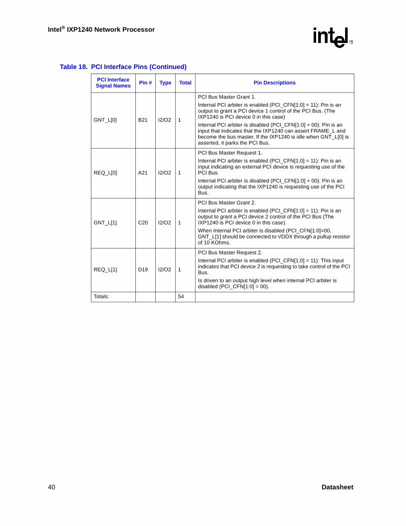
Intel® IXP1240 Network Processor
GNT_L[0] B21 I2/O2 1
PCI Bus Master Grant 1.
Internal PCI arbiter is enabled (PCI_CFN[1:0] = 11): Pin is an output to grant a PCI device 1 control of the PCI Bus. (The IXP1240 is PCI device 0 in this case)
Internal PCI arbiter is disabled (PCI_CFN[1:0] = 00): Pin is an input that indicates that the IXP1240 can assert FRAME_L and become the bus master. If the IXP1240 is idle when GNT_L[0] is asserted, it parks the PCI Bus.
REQ_L[0] A21 I2/O2 1
PCI Bus Master Request 1.
Internal PCI arbiter is enabled (PCI_CFN[1:0] = 11): Pin is an input indicating an external PCI device is requesting use of the PCI Bus.
Internal PCI arbiter is disabled (PCI_CFN[1:0] = 00): Pin is an output indicating that the IXP1240 is requesting use of the PCI Bus.
GNT_L[1] C20 I2/O2 1
PCI Bus Master Grant 2.
Internal PCI arbiter is enabled (PCI_CFN[1:0] = 11): Pin is an output to grant a PCI device 2 control of the PCI Bus (The IXP1240 is PCI device 0 in this case).
When Internal PCI arbiter is disabled (PCI_CFN[1:0]=00, GNT_L[1] should be connected to VDDX through a pullup resistor of 10 KOhms.
REQ_L[1] D19 I2/O2 1
PCI Bus Master Request 2.
Internal PCI arbiter is enabled (PCI_CFN[1:0] = 11): This input indicates that PCI device 2 is requesting to take control of the PCI Bus.
Is driven to an output high level when internal PCI arbiter is disabled (PCI_CFN[1:0] = 00).
Totals: 54
Table 18. PCI Interface Pins (Continued)
PCI Interface Signal Names Pin # Type Total Pin Descriptions
40 Datasheet
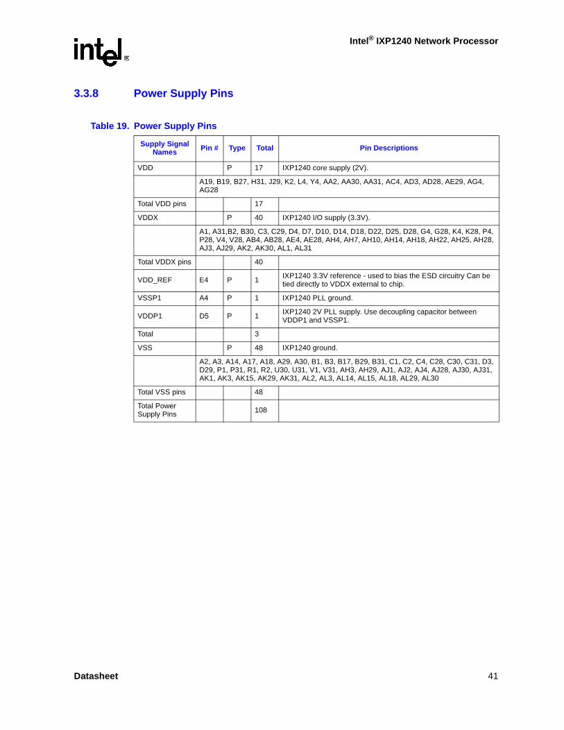
Intel® IXP1240 Network Processor
3.3.8 Power Supply Pins
Table 19. Power Supply Pins
Supply Signal Names Pin # Type Total Pin Descriptions
VDD P 17 IXP1240 core supply (2V).
A19, B19, B27, H31, J29, K2, L4, Y4, AA2, AA30, AA31, AC4, AD3, AD28, AE29, AG4, AG28
Total VDD pins 17
VDDX P 40 IXP1240 I/O supply (3.3V).
A1, A31,B2, B30, C3, C29, D4, D7, D10, D14, D18, D22, D25, D28, G4, G28, K4, K28, P4, P28, V4, V28, AB4, AB28, AE4, AE28, AH4, AH7, AH10, AH14, AH18, AH22, AH25, AH28, AJ3, AJ29, AK2, AK30, AL1, AL31
Total VDDX pins 40
VDD_REF E4 P 1 IXP1240 3.3V reference - used to bias the ESD circuitry Can be tied directly to VDDX external to chip.
VSSP1 A4 P 1 IXP1240 PLL ground.
VDDP1 D5 P 1 IXP1240 2V PLL supply. Use decoupling capacitor between VDDP1 and VSSP1.
Total 3
VSS P 48 IXP1240 ground.
A2, A3, A14, A17, A18, A29, A30, B1, B3, B17, B29, B31, C1, C2, C4, C28, C30, C31, D3, D29, P1, P31, R1, R2, U30, U31, V1, V31, AH3, AH29, AJ1, AJ2, AJ4, AJ28, AJ30, AJ31, AK1, AK3, AK15, AK29, AK31, AL2, AL3, AL14, AL15, AL18, AL29, AL30
Total VSS pins 48
Total Power Supply Pins 108
Datasheet 41

Intel® IXP1240 Network Processor
3.3.9 IEEE 1149.1 Interface Pins
3.3.10 Miscellaneous Test Pins
Table 20. IEEE 1149.1 Interface Pins
IEEE 1149.1 Interface Pin
NamePin # Type Total Pin Description
TCK A23 I1 1 Test Interface reference clock. This clock times all the transfers on the IEEE 1149.1 test interface.
TMS C22 I1 1 Test Interface mode select. Causes state transitions on the test access port (TAP) controller.
TDI B22 I1 1 Test Interface data input. The serial input through which IEEE 1149.1 instructions and test data enter the IEEE 1149.1 interface.
TDO D21 O1 1 Test Interface data output. The serial output through which test instruction and data from the test logic leave the IXP1240.
TRST_L B23 I1 1
Test Interface RESET. When asserted low, the TAP controller is asynchronously forced to enter a reset state, and disables the IEEE 1149.1 port. This pin must be driven or held low to achieve normal device operation.
Totals: 5
Table 21. Miscellaneous Test Pins
Processor Support Signal
NamesPin # Type Total Pin Descriptions
SCAN_EN C5 I1 1Used for Intel test purposes only. Enables internal scan chains for chip testing. This pin should be connected to VSS through a pulldown resistor.
TCK_BYP D6 I1 1 Used for Intel test purposes only. When high, bypasses PLL for Test/debug. Must be low for normal system operation.
TSTCLK B5 I1 1
Used for Intel test purposes only. Used as clock input when bypassing the internal PLL clock generator. For Normal operation, this pin should not be allowed to float. It should be pulled up or pulled down through the proper value resistor.
Totals: 3
42 Datasheet

Intel® IXP1240 Network Processor
3.3.11 Pin Usage Summary
Table 22. Pin Usage Summary
Type Quantity
Inputs 21
Outputs 68
Bidirectional 235
Total Signal 324
Power 108
Overall Totals: 432
Datasheet 43
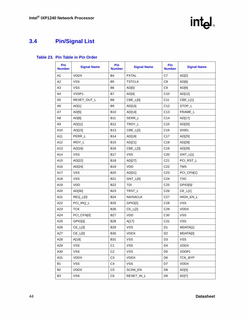
Intel® IXP1240 Network Processor
3.4 Pin/Signal List
Table 23. Pin Table in Pin Order
Pin Number Signal Name Pin
Number Signal Name Pin Number Signal Name
A1 VDDX B4 PXTAL C7 AD[2]
A2 VSS B5 TSTCLK C8 AD[6]
A3 VSS B6 AD[0] C9 AD[9]
A4 VSSP1 B7 AD[4] C10 AD[12]
A5 RESET_OUT_L B8 CBE_L[0] C11 CBE_L[1]
A6 AD[1] B9 AD[10] C12 STOP_L
A7 AD[5] B10 AD[14] C13 FRAME_L
A8 AD[8] B11 SERR_L C14 AD[17]
A9 AD[11] B12 TRDY_L C15 AD[20]
A10 AD[15] B13 CBE_L[2] C16 IDSEL
A11 PERR_L B14 AD[19] C17 AD[25]
A12 IRDY_L B15 AD[21] C18 AD[28]
A13 AD[16] B16 CBE_L[3] C19 AD[29]
A14 VSS B17 VSS C20 GNT_L[1]
A15 AD[22] B18 AD[27] C21 PCI_RST_L
A16 AD[24] B19 VDD C22 TMS
A17 VSS B20 AD[31] C23 PCI_CFN[1]
A18 VSS B21 GNT_L[0] C24 TXD
A19 VDD B22 TDI C25 GPIO[0]/
A20 AD[30] B23 TRST_L C26 CE_L[1]
A21 REQ_L[0] B24 NA/SACLK C27 HIGH_EN_L
A22 PCI_IRQ_L B25 GPIO[2] C28 VSS
A23 TCK B26 CE_L[2] C29 VDDX
A24 PCI_CFN[0] B27 VDD C30 VSS
A25 GPIO[3] B28 A[17] C31 VSS
A26 CE_L[3] B29 VSS D1 MDATA[1]
A27 CE_L[0] B30 VDDX D2 MDATA[0]
A28 A[18] B31 VSS D3 VSS
A29 VSS C1 VSS D4 VDDX
A30 VSS C2 VSS D5 VDDP1
A31 VDDX C3 VDDX D6 TCK_BYP
B1 VSS C4 VSS D7 VDDX
B2 VDDX C5 SCAN_EN D8 AD[3]
B3 VSS C6 RESET_IN_L D9 AD[7]
44 Datasheet
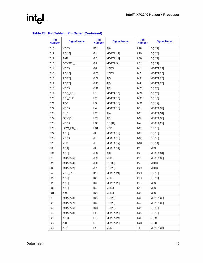
Intel® IXP1240 Network Processor
D10 VDDX F31 A[6] L28 DQ[27]
D11 AD[13] G1 MDATA[12] L29 DQ[24]
D12 PAR G2 MDATA[11] L30 DQ[22]
D13 DEVSEL_L G3 MDATA[9] L31 DQ[21]
D14 VDDX G4 VDDX M1 MDATA[29]
D15 AD[18] G28 VDDX M2 MDATA[28]
D16 AD[23] G29 A[5] M3 MDATA[26]
D17 AD[26] G30 A[3] M4 MDATA[23]
D18 VDDX G31 A[2] M28 DQ[23]
D19 REQ_L[1] H1 MDATA[16] M29 DQ[20]
D20 PCI_CLK H2 MDATA[15] M30 DQ[18]
D21 TDO H3 MDATA[13] M31 DQ[17]
D22 VDDX H4 MDATA[10] N1 MDATA[32]
D23 RXD H28 A[4] N2 MDATA[31]
D24 GPIO[1] H29 A[1] N3 MDATA[30]
D25 VDDX H30 DQ[31] N4 MDATA[27]
D26 LOW_EN_L H31 VDD N28 DQ[19]
D27 A[16] J1 MDATA[19] N29 DQ[16]
D28 VDDX J2 MDATA[18] N30 DQ[15]
D29 VSS J3 MDATA[17] N31 DQ[14]
D30 A[14] J4 MDATA[14] P1 VSS
D31 A[13] J28 A[0] P2 MDATA[34]
E1 MDATA[5] J29 VDD P3 MDATA[33]
E2 MDATA[4] J30 DQ[30] P4 VDDX
E3 MDATA[2] J31 DQ[29] P28 VDDX
E4 VDD_REF K1 MDATA[21] P29 DQ[13]
E28 A[15] K2 VDD P30 DQ[11]
E29 A[12] K3 MDATA[20] P31 VSS
E30 A[10] K4 VDDX R1 VSS
E31 A[9] K28 VDDX R2 VSS
F1 MDATA[8] K29 DQ[28] R3 MDATA[36]
F2 MDATA[7] K30 DQ[26] R4 MDATA[35]
F3 MDATA[6] K31 DQ[25] R28 DQ[12]
F4 MDATA[3] L1 MDATA[25] R29 DQ[10]
F28 A[11] L2 MDATA[24] R30 DQ[9]
F29 A[8] L3 MDATA[22] R31 DQ[8]
F30 A[7] L4 VDD T1 MDATA[37]
Table 23. Pin Table in Pin Order (Continued)
Pin Number Signal Name Pin
Number Signal Name Pin Number Signal Name
Datasheet 45

Intel® IXP1240 Network Processor
T2 MDATA[38] Y31 MRD_L AE28 VDDX
T3 MDATA[39] AA1 MADR[4] AE29 VDD
T4 MDATA[40] AA2 VDD AE30 FDAT[60]
T28 DQ[7] AA3 MADR[5] AE31 FDAT[61]
T29 DQ[6] AA4 MADR[8] AF1 MDATA[50]
T30 DQ[5] AA28 PORTCTL_L[0] AF2 MDATA[51]
T31 DQ[4] AA29 TK_OUT AF3 MDATA[52]
U1 MDATA[41] AA30 VDD AF4 MDATA[55]
U2 MDATA[42] AA31 VDD AF28 FDAT[54]
U3 MDATA[43] AB1 MADR[6] AF29 FDAT[57]
U4 MDATA[45] AB2 MADR[7] AF30 FDAT[58]
U28 DQ[2] AB3 MADR[9] AF31 FDAT[59]
U29 DQ[3] AB4 VDDX AG1 MDATA[53]
U30 VSS AB28 VDDX AG2 MDATA[54]
U31 VSS AB29 PORTCTL_L[1] AG3 MDATA[56]
V1 VSS AB30 FCLK AG4 VDD
V2 MDATA[44] AB31 TK_IN AG28 VDD
V4 VDDX AC1 MADR[10] AG29 FDAT[53]
V28 VDDX AC2 MADR[11] AG30 FDAT[55]
V29 DQ[0] AC3 MADR[12] AG31 FDAT[56]
V30 DQ[1] AC4 VDD AH1 MDATA[57]
V31 VSS AC28 FDAT[63] AH2 MDATA[58]
W1 WE_L AC29 FPS[2] AH3 VSS
W2 RAS_L AC30 PORTCTL_L[3] AH4 VDDX
W3 CAS_L AC31 PORTCTL_L[2] AH5 MDATA[59]
W4 MADR[2] AD1 MADR[13] AH6 MDATA[63]
W28 FWE_L AD2 SDCLK AH7 VDDX
W29 MCE_L AD3 VDD AH8 RDYCTL_L[1]
W30 SOE_L AD4 MDATA[48] AH9 RDYBUS[2]
W31 SCLK AD28 VDD AH10 VDDX
Y1 MADR[0] AD29 FDAT[62] AH11 FAST_RX1
Y2 MADR[1] AD30 FPS[0] AH12 SOP
Y3 MADR[3] AD31 FPS[1] AH13 FBE_L[3]
Y4 VDD AE1 MDATA[46] AH14 VDDX
Y28 CINT_L AE2 MDATA[47] AH15 FDAT[3]
Y29 SLOW_EN_L AE3 MDATA[49] AH16 FDAT[8]
Y30 SWE_L AE4 VDDX AH17 FDAT[13]
Table 23. Pin Table in Pin Order (Continued)
Pin Number Signal Name Pin
Number Signal Name Pin Number Signal Name
46 Datasheet

Intel® IXP1240 Network Processor
AH18 VDDX AJ23 FDAT[32] AK28 FDAT[49]
AH19 FDAT[20] AJ24 FDAT[36] AK29 VSS
AH20 FDAT[24] AJ25 FDAT[40] AK30 VDDX
AH21 FDAT[28] AJ26 FDAT[43] AK31 VSS
AH22 VDDX AJ27 FDAT[47] AL1 VDDX
AH23 FDAT[35] AJ28 VSS AL2 VSS
AH24 FDAT[39] AJ29 VDDX AL3 VSS
AH25 VDDX AJ30 VSS AL4 MDATA[61]
AH26 FDAT[46] AJ31 VSS AL5 EOP32
AH27 FDAT[50] AK1 VSS AL6 RDYCTL_L[3]
AH28 VDDX AK2 VDDX AL7 RDYBUS[0]
AH29 VSS AK3 VSS AL8 RDYBUS[4]
AH30 FDAT[51] AK4 MDATA[60] AL9 RDYBUS[7]
AH31 FDAT[52] AK5 MADR[14] AL10 TXASIS
AJ1 VSS AK6 RDYCTL_L[4] AL11 FBE_L[1]
AJ2 VSS AK7 RDYCTL_L[0] AL12 FBE_L[5]
AJ3 VDDX AK8 RDYBUS[3] AL13 FDAT[0]
AJ4 VSS AK9 RDYBUS[6] AL14 VSS
AJ5 MDATA[62] AK10 RXFAIL AL15 VSS
AJ6 SOP32 AK11 FBE_L[0] AL16 FDAT[5]
AJ7 RDYCTL_L[2] AK12 FBE_L[4] AL17 FDAT[9]
AJ8 RDYBUS[1] AK13 FBE_L[7] AL18 VSS
AJ9 RDYBUS[5] AK14 FDAT[2] AL19 FDAT[15]
AJ10 FAST_RX2 AK15 VSS AL20 FDAT[18]
AJ11 EOP AK16 FDAT[6] AL21 FDAT[22]
AJ12 FBE_L[2] AK17 FDAT[10] AL22 FDAT[26]
AJ13 FBE_L[6] AK18 FDAT[12] AL23 FDAT[30]
AJ14 FDAT[1] AK19 FDAT[16] AL24 FDAT[33]
AJ15 FDAT[4] AK20 FDAT[19] AL25 FDAT[37]
AJ16 FDAT[7] AK21 FDAT[23] AL26 FDAT[41]
AJ17 FDAT[11] AK22 FDAT[27] AL27 FDAT[44]
AJ18 FDAT[14] AK23 FDAT[31] AL28 FDAT[48]
AJ19 FDAT[17] AK24 FDAT[34] AL29 VSS
AJ20 FDAT[21] AK25 FDAT[38] AL30 VSS
AJ21 FDAT[25] AK26 FDAT[42] AL31 VDDX
AJ22 FDAT[29] AK27 FDAT[45]
Table 23. Pin Table in Pin Order (Continued)
Pin Number Signal Name Pin
Number Signal Name Pin Number Signal Name
Datasheet 47

Intel® IXP1240 Network Processor
3.5 Signals Listed in Alphabetical Order
Table 24. Pin Table in Alphabetical Order
Signal Name Pin Number Signal Name Pin
Number Signal Name Pin Number
A[0] J28 AD[22] A15 DQ[14] N31
A[1] H29 AD[23] D16 DQ[15] N30
A[10] E30 AD[24] A16 DQ[16] N29
A[11] F28 AD[25] C17 DQ[17] M31
A[12] E29 AD[26] D17 DQ[18] M30
A[13] D31 AD[27] B18 DQ[19] N28
A[14] D30 AD[28] C18 DQ[2] U28
A[15] E28 AD[29] C19 DQ[20] M29
A[16] D27 AD[3] D8 DQ[21] L31
A[17] B28 AD[30] A20 DQ[22] L30
A[18] A28 AD[31] B20 DQ[23] M28
A[2] G31 AD[4] B7 DQ[24] L29
A[3] G30 AD[5] A7 DQ[25] K31
A[4] H28 AD[6] C8 DQ[26] K30
A[5] G29 AD[7] D9 DQ[27] L28
A[6] F31 AD[8] A8 DQ[28] K29
A[7] F30 AD[9] C9 DQ[29] J31
A[8] F29 CAS_L W3 DQ[3] U29
A[9] E31 CBE_L[0] B8 DQ[30] J30
AD[0] B6 CBE_L[1] C11 DQ[31] H30
AD[1] A6 CBE_L[2] B13 DQ[4] T31
AD[10] B9 CBE_L[3] B16 DQ[5] T30
AD[11] A9 CE_L[0] A27 DQ[6] T29
AD[12] C10 CE_L[1] C26 DQ[7] T28
AD[13] D11 CE_L[2] B26 DQ[8] R31
AD[14] B10 CE_L[3] A26 DQ[9] R30
AD[15] A10 CINT_L Y28 DQM V3
AD[16] A13 DEVSEL_L D13 EOP AJ11
AD[17] C14 DQ[0] V29 EOP32 AL5
AD[18] D15 DQ[1] V30 FAST_RX1 AH11
AD[19] B14 DQ[10] R29 FAST_RX2 AJ10
AD[2] C7 DQ[11] P30 FBE_L[0] AK11
AD[20] C15 DQ[12] R28 FBE_L[1] AL11
AD[21] B15 DQ[13] P29 FBE_L[2] AJ12
48 Datasheet

Intel® IXP1240 Network Processor
FBE_L[3] AH13 FDAT[37] AL25 FWE_L W28
FBE_L[4] AK12 FDAT[38] AK25 GNT_L[0] B21
FBE_L[5] AL12 FDAT[39] AH24 GNT_L[1] C20
FBE_L[6] AJ13 FDAT[4] AJ15 GPIO[0] C25
FBE_L[7] AK13 FDAT[40] AJ25 GPIO[1] D24
FCLK AB30 FDAT[41] AL26 GPIO[2] B25
FDAT[0] AL13 FDAT[42] AK26 GPIO[3] A25
FDAT[1] AJ14 FDAT[43] AJ26 HIGH_EN_L C27
FDAT[10] AK17 FDAT[44] AL27 IDSEL C16
FDAT[11] AJ17 FDAT[45] AK27 IRDY_L A12
FDAT[12] AK18 FDAT[46] AH26 LOW_EN_L D26
FDAT[13] AH17 FDAT[47] AJ27 MADR[0] Y1
FDAT[14] AJ18 FDAT[48] AL28 MADR[1] Y2
FDAT[15] AL19 FDAT[49] AK28 MADR[10] AC1
FDAT[16] AK19 FDAT[5] AL16 MADR[11] AC2
FDAT[17] AJ19 FDAT[50] AH27 MADR[12] AC3
FDAT[18] AL20 FDAT[51] AH30 MADR[13] AD1
FDAT[19] AK20 FDAT[52] AH31 MADR[14] AK5
FDAT[2] AK14 FDAT[53] AG29 MADR[2] W4
FDAT[20] AH19 FDAT[54] AF28 MADR[3] Y3
FDAT[21] AJ20 FDAT[55] AG30 MADR[4] AA1
FDAT[22] AL21 FDAT[56] AG31 MADR[5] AA3
FDAT[23] AK21 FDAT[57] AF29 MADR[6] AB1
FDAT[24] AH20 FDAT[58] AF30 MADR[7] AB2
FDAT[25] AJ21 FDAT[59] AF31 MADR[8] AA4
FDAT[26] AL22 FDAT[6] AK16 MADR[9] AB3
FDAT[27] AK22 FDAT[60] AE30 MCE_L W29
FDAT[28] AH21 FDAT[61] AE31 MDATA[0] D2
FDAT[29] AJ22 FDAT[62] AD29 MDATA[1] D1
FDAT[3] AH15 FDAT[63] AC28 MDATA[10] H4
FDAT[30] AL23 FDAT[7] AJ16 MDATA[11] G2
FDAT[31] AK23 FDAT[8] AH16 MDATA[12] G1
FDAT[32] AJ23 FDAT[9] AL17 MDATA[13] H3
FDAT[33] AL24 FPS[0] AD30 MDATA[14] J4
FDAT[34] AK24 FPS[1] AD31 MDATA[15] H2
FDAT[35] AH23 FPS[2] AC29 MDATA[16] H1
FDAT[36] AJ24 FRAME_L C13 MDATA[17] J3
Table 24. Pin Table in Alphabetical Order (Continued)
Signal Name Pin Number Signal Name Pin
Number Signal Name Pin Number
Datasheet 49
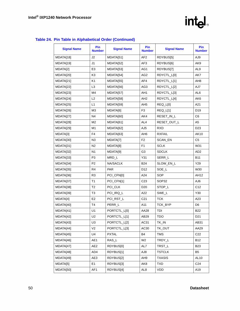
Intel® IXP1240 Network Processor
MDATA[18] J2 MDATA[51] AF2 RDYBUS[5] AJ9
MDATA[19] J1 MDATA[52] AF3 RDYBUS[6] AK9
MDATA[2] E3 MDATA[53] AG1 RDYBUS[7] AL9
MDATA[20] K3 MDATA[54] AG2 RDYCTL_L[0] AK7
MDATA[21] K1 MDATA[55] AF4 RDYCTL_L[1] AH8
MDATA[22] L3 MDATA[56] AG3 RDYCTL_L[2] AJ7
MDATA[23] M4 MDATA[57] AH1 RDYCTL_L[3] AL6
MDATA[24] L2 MDATA[58] AH2 RDYCTL_L[4] AK6
MDATA[25] L1 MDATA[59] AH5 REQ_L[0] A21
MDATA[26] M3 MDATA[6] F3 REQ_L[1] D19
MDATA[27] N4 MDATA[60] AK4 RESET_IN_L C6
MDATA[28] M2 MDATA[61] AL4 RESET_OUT_L A5
MDATA[29] M1 MDATA[62] AJ5 RXD D23
MDATA[3] F4 MDATA[63] AH6 RXFAIL AK10
MDATA[30] N3 MDATA[7] F2 SCAN_EN C5
MDATA[31] N2 MDATA[8] F1 SCLK W31
MDATA[32] N1 MDATA[9] G3 SDCLK AD2
MDATA[33] P3 MRD_L Y31 SERR_L B11
MDATA[34] P2 NA/SACLK B24 SLOW_EN_L Y29
MDATA[35] R4 PAR D12 SOE_L W30
MDATA[36] R3 PCI_CFN[0] A24 SOP AH12
MDATA[37] T1 PCI_CFN[1] C23 SOP32 AJ6
MDATA[38] T2 PCI_CLK D20 STOP_L C12
MDATA[39] T3 PCI_IRQ_L A22 SWE_L Y30
MDATA[4] E2 PCI_RST_L C21 TCK A23
MDATA[40] T4 PERR_L A11 TCK_BYP D6
MDATA[41] U1 PORTCTL_L[0] AA28 TDI B22
MDATA[42] U2 PORTCTL_L[1] AB29 TDO D21
MDATA[43] U3 PORTCTL_L[2] AC31 TK_IN AB31
MDATA[44] V2 PORTCTL_L[3] AC30 TK_OUT AA29
MDATA[45] U4 PXTAL B4 TMS C22
MDATA[46] AE1 RAS_L W2 TRDY_L B12
MDATA[47] AE2 RDYBUS[0] AL7 TRST_L B23
MDATA[48] AD4 RDYBUS[1] AJ8 TSTCLK B5
MDATA[49] AE3 RDYBUS[2] AH9 TXASIS AL10
MDATA[5] E1 RDYBUS[3] AK8 TXD C24
MDATA[50] AF1 RDYBUS[4] AL8 VDD A19
Table 24. Pin Table in Alphabetical Order (Continued)
Signal Name Pin Number Signal Name Pin
Number Signal Name Pin Number
50 Datasheet

Intel® IXP1240 Network Processor
VDD B19 VDDX P28 VSS C30
VDD B27 VDDX V4 VSS C31
VDD H31 VDDX V28 VSS D3
VDD J29 VDDX AB4 VSS D29
VDD K2 VDDX AB28 VSS P1
VDD L4 VDDX AE4 VSS P31
VDD Y4 VDDX AE28 VSS R1
VDD AA2 VDDX AH4 VSS R2
VDD AA30 VDDX AH7 VSS U30
VDD AA31 VDDX AH10 VSS U31
VDD AC4 VDDX AH14 VSS V1
VDD AD3 VDDX AH18 VSS V31
VDD AD28 VDDX AH22 VSS AH3
VDD AE29 VDDX AH25 VSS AH29
VDD AG4 VDDX AH28 VSS AJ1
VDD AG28 VDDX AJ3 VSS AJ2
VDD_REF E4 VDDX AJ29 VSS AJ4
VDDP1 D5 VDDX AK2 VSS AJ28
VDDX A1 VDDX AK30 VSS AJ30
VDDX A31 VDDX AL1 VSS AJ31
VDDX B2 VDDX AL31 VSS AK1
VDDX B30 VSS A2 VSS AK3
VDDX C3 VSS A3 VSS AK15
VDDX C29 VSS A14 VSS AK29
VDDX D4 VSS A17 VSS AK31
VDDX D7 VSS A18 VSS AL2
VDDX D10 VSS A29 VSS AL3
VDDX D14 VSS A30 VSS AL14
VDDX D18 VSS B1 VSS AL15
VDDX D22 VSS B3 VSS AL18
VDDX D25 VSS B17 VSS AL29
VDDX D28 VSS B29 VSS AL30
VDDX G4 VSS B31 VSSP1 A4
VDDX G28 VSS C1 WE_L W1
VDDX K4 VSS C2
VDDX K28 VSS C4
VDDX P4 VSS C28
Table 24. Pin Table in Alphabetical Order (Continued)
Signal Name Pin Number Signal Name Pin
Number Signal Name Pin Number
Datasheet 51

Intel® IXP1240 Network Processor
3.6 IX Bus Pins Function Listed by Operating Mode
Figure 7 through Figure 11 illustrate the four IX Bus modes. Each figure shows the logic interface to one or more MAC devices and is accompanied by a pin description for the IX Bus in that mode.
Figure 7. 64-Bit Bidirectional IX Bus, 1-2 MAC Mode
A8871-01
wireorCINT_L
RDYBUS[7:0]
RDYCTL_L[4:0]
PORTCTL_L[3:0]
[0][1]
[0]
[2]
FBE_L[7:0]
EOP
CINT[7:0]
TxRDY[7:0]
TxCTL_L
RxRDY[7:0]
FLCTL[7:0]
RxCTL_L
RxSEL_L
MAC1
TxSEL_L
[2][3]
[1][3]
FDAT[63:0]
SOP
FPS[2:0]
FBE_L[7:0]
RxFAIL
EOPTXAXIS
SOP32
TXAXIS
EOP32
FPS[2:0]
SOP
FDAT[63:0]
[4]
FCLK
FCLK
DQe
GPIO[0]not usedGPIO[3:1]
CINT[7:0]
TxRDY[7:0]
TxCTL_L
RxRDY[7:0]
FLCTL[7:0]
RxCTL_L
RxSEL_L
MAC0
TxSEL_L
FPS[2:0]
FBE_L[7:0]
SOP
FDAT[63:0]
EOPTXAXIS
RxFAIL RxFAIL
Intel® IXP1240Processor
3.3V
not used
DQe
3.3V
52 Datasheet
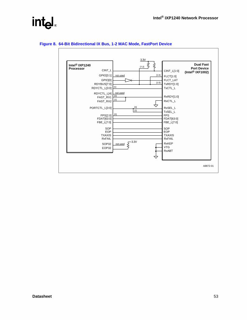
Intel® IXP1240 Network Processor
Figure 8. 64-Bit Bidirectional IX Bus, 1-2 MAC Mode, FastPort Device
A8872-01
[1]
[7:2]
[1:0]
[1:0]
[0]
[1]
[0]
[0]
[2]
not used
not used
not used
3.3V
CINT_L[1:0]
TxRDY[1:0]TxCTL_L
RxRDY[1:0]
FLCT[1:0]FLCT_LAT
RxSEL_LTxSEL_LFPSFDAT[63:0]FBE_L[7:0]
EOPSOP
TXAXIS
Dual FastPort Device
(Intel® IXF1002)CINT_L
RDYBUS[7:0]RDYCTL_L[3:0]
PORTCTL_L[3:0]
FAST_RX1RxCTL_LFAST_RX2
FPS[2:0]FDAT[63:0]FBE_L[7:0]
SOPEOP
TXAXISRxFAIL RxFAIL
GPIO[0]
GPIO[3:1]
SOP32EOP32
Intel® IXP1240Processor
RDYCTL_L[4]
RxKEPVTGRxABT
3.3V
Datasheet 53

Intel® IXP1240 Network Processor
Table 25. 64-Bit Bidirectional IX Bus, 1-2 MAC Mode
Signal Description
GPIO[3:1] Active High, input/output assigned to StrongARM* core not used for MAC interface.
GPIO[0 Active Low, output flow-control enable for MAC 0.
RDYCTL_L[3:0] Active Low, output, enables for Transmit or Receive Ready flags.
RDYCTL_L[4] Active Low, output, flow-control enable for MAC 1.
RDYBUS[7:0] Active High, input/output, Transmit or Receive Ready flags, and flow control mask data.
PORTCTL_L[3:0] Active Low, output, transmit and receive device selects.
FPS[2:0] Active High, output, port select.
SOPActive High, input/output, Start of Packet indication. SOP is an output during transmit according to values programmed in the TFIFO control field. Is an input during receives indicating Receive Start of Packet from MAC.
SOP32 Output, not used, no connect.
EOPActive High, input/output, End of Packet indication. EOP is an output during transmit according to values programmed in the TFIFO control field. Is an input during receives indicating Receive End of Packet from MAC.
EOP32 Input/output, not used, terminate through 10 KOhms to VDDX.
TK_IN Input, not used, must be pulled High in this mode.
TK_OUT Output, not used, no connect.
RXFAIL
Active High, input/output.
Input - Receive Error input.
Output - driven low during transmit and when bus maintains a No-Select state.
TXASIS Active High, output. TXASIS states are output according to values programmed in the TFIFO Control field. TXASIS state is output coincident with SOP signal,
FBE_L[7:0] Active Low, byte enables for FDAT [64:0].
FDAT[63:0] Active High, read and write data.
FAST_RX1 Active High ready input from FastPort 0, pulldown 10 KOhms to GND if not used.
FAST_RX2 Active High ready input from FastPort 1, pulldown 10 KOhms to GND if not used.
54 Datasheet

Intel® IXP1240 Network Processor
Figure 9. 64-Bit Bidirectional IX Bus, 3+ MAC Mode
A8873-01
wireor
[20][24]
CINT[7:0]
TxRDY[7:0]
TxCTL_L
RxRDY[7:0]
FLCTL[7:0]
RxCTL_L
RxSEL_LTxSEL_LFPS[2:0]FDAT[63:0]FBE_L[7:0]SOPEOPTXAXISRxFAIL
CINT[7:0]
TxRDY[7:0]
TxCTL_L
RxRDY[7:0]
FLCTL[7:0]
RxCTL_L
RxSEL_LTxSEL_LFPS[2:0]FDAT[63:0]FBE_L[7:0]
SOPEOPTXAXISRxFAIL
[27]
[23]
[1]
[0]
[7][6]
[19]
[16]
MAC0
MAC3
5 > 32[31:0]
[15:0]
CINT_L
RDYBUS[7:0]RDYCTL_L[4:0]
PORTCTL_L[3:0]
FPS[2:0]FDAT[63:0]FBE_L[7:0]
SOPEOP
TXAXISRxFAIL
GPIO[3:0]
SOP32EOP32
Intel® IXP1240Processor
not used
not used
FCLK
FCLK
FCLK
FCLK
D Qe
D Qe
3.3V
4 > 16
3.3V
Datasheet 55
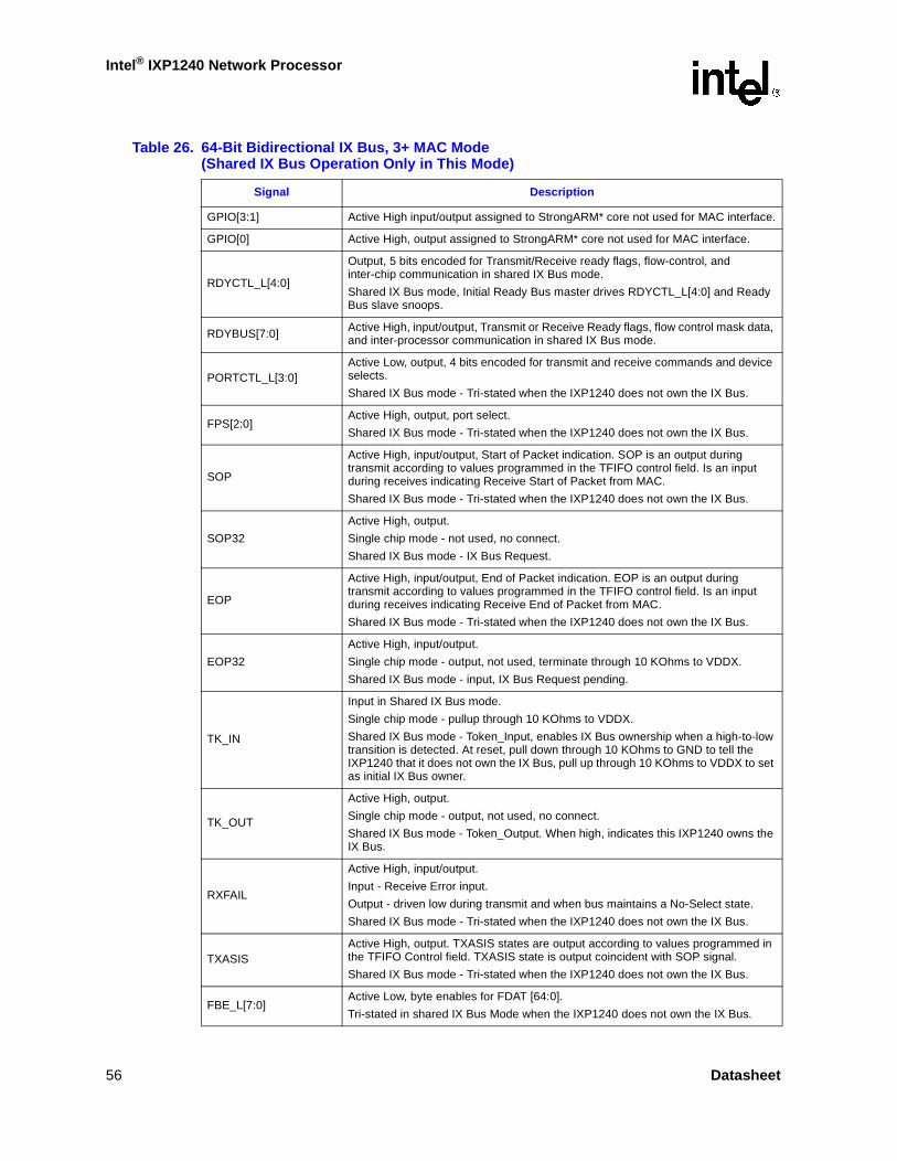
Intel® IXP1240 Network Processor
Table 26. 64-Bit Bidirectional IX Bus, 3+ MAC Mode(Shared IX Bus Operation Only in This Mode)
Signal Description
GPIO[3:1] Active High input/output assigned to StrongARM* core not used for MAC interface.
GPIO[0] Active High, output assigned to StrongARM* core not used for MAC interface.
RDYCTL_L[4:0]
Output, 5 bits encoded for Transmit/Receive ready flags, flow-control, and inter-chip communication in shared IX Bus mode.
Shared IX Bus mode, Initial Ready Bus master drives RDYCTL_L[4:0] and Ready Bus slave snoops.
RDYBUS[7:0] Active High, input/output, Transmit or Receive Ready flags, flow control mask data, and inter-processor communication in shared IX Bus mode.
PORTCTL_L[3:0]Active Low, output, 4 bits encoded for transmit and receive commands and device selects.
Shared IX Bus mode - Tri-stated when the IXP1240 does not own the IX Bus.
FPS[2:0]Active High, output, port select.
Shared IX Bus mode - Tri-stated when the IXP1240 does not own the IX Bus.
SOP
Active High, input/output, Start of Packet indication. SOP is an output during transmit according to values programmed in the TFIFO control field. Is an input during receives indicating Receive Start of Packet from MAC.
Shared IX Bus mode - Tri-stated when the IXP1240 does not own the IX Bus.
SOP32
Active High, output.
Single chip mode - not used, no connect.
Shared IX Bus mode - IX Bus Request.
EOP
Active High, input/output, End of Packet indication. EOP is an output during transmit according to values programmed in the TFIFO control field. Is an input during receives indicating Receive End of Packet from MAC.
Shared IX Bus mode - Tri-stated when the IXP1240 does not own the IX Bus.
EOP32
Active High, input/output.
Single chip mode - output, not used, terminate through 10 KOhms to VDDX.
Shared IX Bus mode - input, IX Bus Request pending.
TK_IN
Input in Shared IX Bus mode.
Single chip mode - pullup through 10 KOhms to VDDX.
Shared IX Bus mode - Token_Input, enables IX Bus ownership when a high-to-low transition is detected. At reset, pull down through 10 KOhms to GND to tell the IXP1240 that it does not own the IX Bus, pull up through 10 KOhms to VDDX to set as initial IX Bus owner.
TK_OUT
Active High, output.
Single chip mode - output, not used, no connect.
Shared IX Bus mode - Token_Output. When high, indicates this IXP1240 owns the IX Bus.
RXFAIL
Active High, input/output.
Input - Receive Error input.
Output - driven low during transmit and when bus maintains a No-Select state.
Shared IX Bus mode - Tri-stated when the IXP1240 does not own the IX Bus.
TXASISActive High, output. TXASIS states are output according to values programmed in the TFIFO Control field. TXASIS state is output coincident with SOP signal.
Shared IX Bus mode - Tri-stated when the IXP1240 does not own the IX Bus.
FBE_L[7:0]Active Low, byte enables for FDAT [64:0].
Tri-stated in shared IX Bus Mode when the IXP1240 does not own the IX Bus.
56 Datasheet
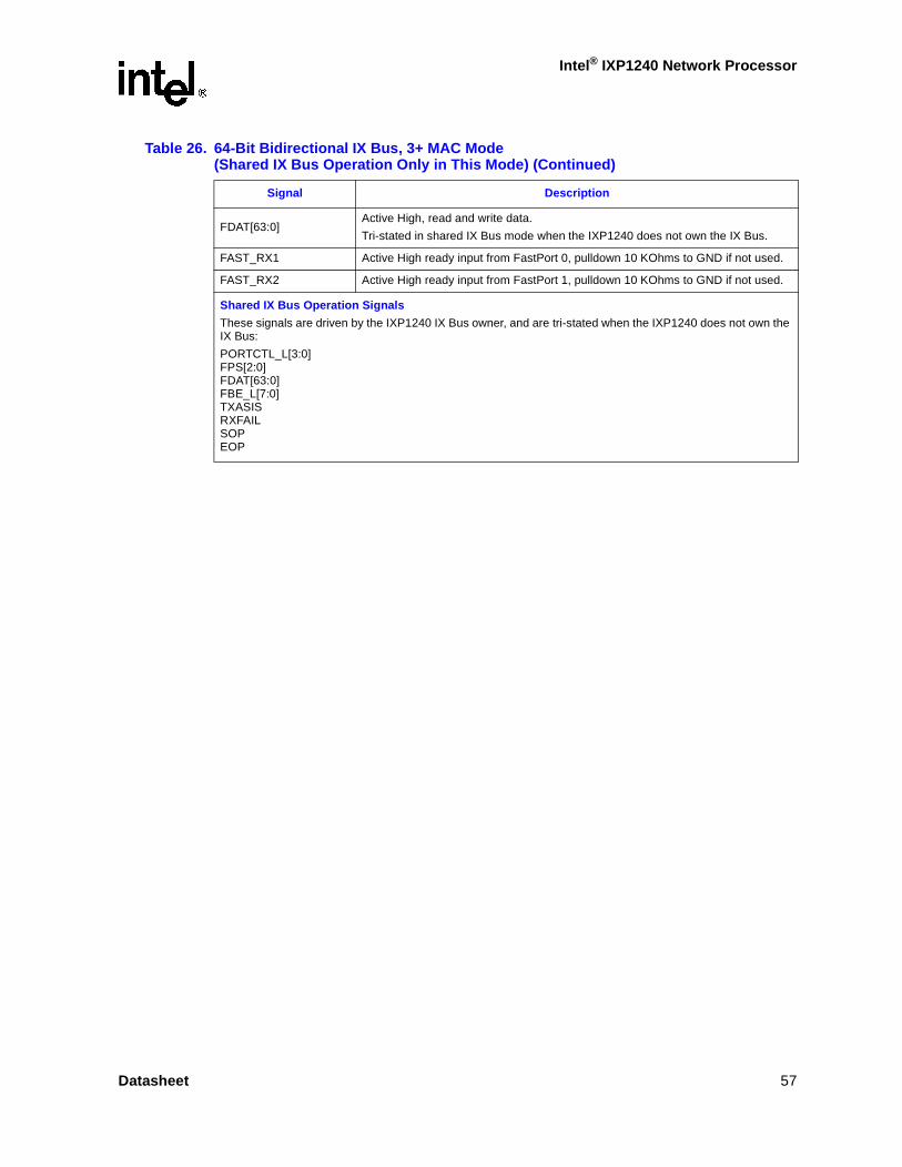
Intel® IXP1240 Network Processor
FDAT[63:0]Active High, read and write data.
Tri-stated in shared IX Bus mode when the IXP1240 does not own the IX Bus.
FAST_RX1 Active High ready input from FastPort 0, pulldown 10 KOhms to GND if not used.
FAST_RX2 Active High ready input from FastPort 1, pulldown 10 KOhms to GND if not used.
Shared IX Bus Operation Signals
These signals are driven by the IXP1240 IX Bus owner, and are tri-stated when the IXP1240 does not own the IX Bus:
PORTCTL_L[3:0]FPS[2:0]FDAT[63:0]FBE_L[7:0]TXASISRXFAILSOPEOP
Table 26. 64-Bit Bidirectional IX Bus, 3+ MAC Mode(Shared IX Bus Operation Only in This Mode) (Continued)
Signal Description
Datasheet 57

Intel® IXP1240 Network Processor
Figure 10. 32-Bit Unidirectional IX Bus, 1-2 MAC Mode
A8874-01
wireorCINT_L
RDYBUS[7:0]
RDYCTL_L[4:0]
PORTCTL_L[1:0]
[0][1]
[0]
Transmit
Receive
FDAT[63:32]
FDAT [31:0]
EOP[2]
CINT[7:0]
TxRDY[7:0]
TxCTL_L
RxRDY[7:0]
FLCTL[7:0]
RxCTL_L
RxSEL_L
MAC1
RxFDAT[31:0]
[2][3]
[1]
[3]TxSEL_L
RxFPS[2:0]
TxFDAT[31:0]
RxFBE_L[3:0]
RxSOPRxFail
RxEOP
TxEOP
TxASIS
TxFBE_L[7:4]TxFPS[2:0]
TxSOP
SOP32
GPIO[3:1]TXAXIS
FBE_L[7:4]
EOP32
FPS[2:0]FBE_L[3:0]
SOPRxFAIL
PORTCTL_L[3:2]
[4]
FCLK
DQe
FCLK
DQe
[7:0]
[7:0]
GPIO[0]
CINT[7:0]
TxRDY[7:0]
TxCTL_L
RxRDY[7:0]
FLCTL[7:0]
RxCTL_L
RxSEL_L
MAC0
RxFDAT_L[31:0]
TxSEL_L
RxFPS[2:0]
TxFDAT[31:0]
RxFBE_L[3:0]
RxSOPRxFail
RxEOP
TxEOP
TXAXIS
TxFBE_L[7:4]TxFPS[2:0]
TxSOP
3.3V
Intel® IXP1240Processor
FDAT[63:32]
SOP32
GPIO[3:1]TxASIS/TxERR
FBE_L[7:4]
EOP32
FDAT [31:0]
EOP
FPS[2:0]FBE_L[3:0]
SOPRxFAIL
58 Datasheet

Intel® IXP1240 Network Processor
Table 27. 32-Bit Unidirectional IX Bus, 1-2 MAC Mode
Transmit Path Signals Description
GPIO[3:1] Active high outputs, Transmit Port Select [2:0].
PORTCTL_L[3:2]Active Low, output.
Transmit Device Selects [1:0].
SOP32 Active High, output, transmit Start of Packet. SOP32 is output during transmit according to value programmed in the TFIFO control field.
EOP32 Active High, output, transmit End of Packet. EOP32 is output during transmit according to value programmed in the TFIFO control field.
TXASIS Active High, output. TXASIS states are output according to values programmed in the TFIFO Control field. TXASIS state is output coincident with SOP32 signal.
FBE_L[7:4] Active Low, output, byte enables for FDAT [63:31].
FDAT[63:31] Active High, output, 32-bit transmit data.
Receive Path Signals
FPS[2:0]Active High, output.
Receive Port Selects [2:0].
PORTCTL_L[1:0]Active Low, output.
Receive Device Selects [1:0].
SOP Active High, input/output, input receive Start of Packet from the MAC. Driven as output when bus remains in No-Select state.
EOP Active High, input/output, input receive End of Packet from the MAC. Driven as output when bus remains in No-Select state.
RXFAIL Active High, input/output, input Receive Error indication from the MAC. Driven as output when bus remains in No-Select state.
FBE_L[3:0] Active Low, input/output, input byte enables for FDAT [31:0] from the MAC. Driven as output when bus remains in No-Select state.
FDAT[31:0] Active High, input/output, input 32-bit receive data from the MAC. Driven as output when bus remains in No-Select state.
Control Signals Common to both Transmit/Receive Paths
GPIO[0] Active Low, output, flow-control for MAC 0.
RDYCTL_L[4] Active Low, output, flow-control for MAC 1.
RDYCTL_L[3:0] Active Low enable outputs for Transmit or Receive Ready flags.
RDYBUS[7:0] Active High, input/output, Transmit or Receive Ready flags, and flow control mask data.
TK_IN Input, not used, must be pulled High in this mode.
TK_OUT Output, not used, no connect.
FAST_RX1 Active High, ready input from Fast Port 0, pulldown 10 KOhms if not used.
FAST_RX2 Active High, ready input from Fast Port 1, pulldown 10 KOhms if not used.
Datasheet 59
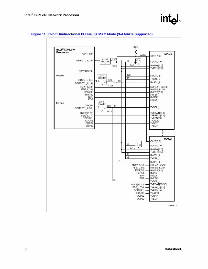
Intel® IXP1240 Network Processor
Figure 11. 32-bit Unidirectional IX Bus, 3+ MAC Mode (3-4 MACs Supported)
A8875-01
wireor
3.3V
[11]
[7]
[0]
[15:0]
[3:0]
[3:0] [0]
CINT[7:0]
TxRDY[7:0]
TxCTL_L
RxRDY[7:0]
FLCTL[7:0]
RxCTL_L
RxSEL_L
MAC3
RxFDAT[31:0]
[8]
[4]
[3]
[3]TxSEL_L
RxFPS[2:0]
TxFDAT[63:32]
RxFBE_L[3:0]
RxSOPRxFail
RxEOP
TxEOP
TXAXIS
TxFBE_L[7:4]TxFPS[2:0]
TxSOP
[0]
D4 > 16decoder
2 > 4decoder
Qe
FCLK
FCLK
[3]
CINT[7:0]
TxRDY[7:0]
TxCTL_L
RxRDY[7:0]
FLCTL[7:0]
RxCTL_L
RxSEL_L
MAC0
RxFDAT_L[31:0]
TxSEL_L
RxFPS[2:0]
TxFDAT[31:0]
RxFBE_L[3:0]
RxSOPRxFail
RxEOP
TxEOP
TXAXIS
TxFBE_L[7:4]TxFPS[2:0]
TxSOP
DQe
CINT_L[0]
RDYBUS[7:0]
RDYCTL_L[3:0]
RDYCTL_L[4]PORTCTL_L[1:0]
Transmit
Receive
FDAT[63:32]
FDAT [31:0]
EOP
SOP32
GPIO[3:1]TXAXIS
FBE_L[7:4]
EOP32
FPS[2:0]FBE_L[3:0]
SOPRxFAIL
PORTCTL_L[3:2]GPIO[0]
FCLK
FCLK
FCLK
Intel® IXP1240Processor
DQe
2 > 4decoder
DQe
FDAT[63:32]
SOP32
GPIO[3:1]TXAXIS
FBE_L[7:4]
EOP32
FDAT [31:0]
EOP
FPS[2:0]FBE_L[3:0]
SOPRxFAIL
60 Datasheet

Intel® IXP1240 Network Processor
Table 28. 32-bit Unidirectional IX Bus, 3+ MAC Mode
Transmit Path Signals Description
GPIO[3:1] Active high outputs, Transmit Port Selects [2:0].
PORTCTL_L[3:2]Active Low, outputs.
Used with GPIO[0]/FC_EN0_L/TXPEN for transmit device select via external 2-to-4 decoder.
GPIO[0]Active High, output, transmit enable.
Used with PORTCTL_L[3:2] for transmit device select via external 2-to-4 decoder.
SOP32 Active High, output, transmit Start of Packet. SOP32 is output during transmit according to values programmed in the TFIFO control field.
EOP32 Active High, output, transmit End of Packet. EOP32 is output during transmit according to values programmed in the TFIFO control field.
TXASIS Active High, output. TXASIS states are output according to values programmed in the TFIFO Control field. TXASIS state is output coincident with SOP32 signal.
FBE_L[7:4] Active Low, output, byte enables for FDAT [63:31].
FDAT[63:31] Active High, output, 32-bit transmit data.
Receive Path Signals
FPS[2:0] Active High, output. Receive Port Selects [2:0].
PORTCTL_L[1:0] Active Low, output. Used with RDYCTL_L[4] for receive device select via external 2-to-4 decoder.
RDYCTL_L[4] Active Low, output, receive enable. Used to enable an external 2-to-4 decoder. Used with PORTCTL_L[1:0].
SOP Active High, input/output, input receive Start of Packet from the MAC. Driven as output when bus remains in No-Select state.
EOP Active High, input/output, input receive End of Packet from the MAC. Driven as output when bus remains in No-Select state.
RXFAIL Active Low, input/output, input Receive Error indication from the MAC. Driven as output when bus remains in No-Select state.
FBE_L[3:0] Active High, input/output, input byte enables for FDAT [31:0] from the MAC. Driven as output when bus remains in No-Select state.
FDAT[31:0] Active High, input/output, input 32-bit receive data from the MAC. Driven as output when bus remains in No-Select state.
Control Signals Common to both Transmit/Receive Paths
RDYCTL_L[3:0] Output, 4 bits encoded for Transmit/Receive Ready flags, flow-control, and inter-chip communication. Decode with external 4-to-16 decoder.
RDYBUS[7:0] Active High, input/output, Transmit or Receive Ready flags, and flow control mask data.
TK_IN Input, not used, must be pulled High in this mode.
TK_OUT Output, not used, no connect.
FAST_RX1 Active High, ready input from Fast Port 0, pulldown 10 KOhms if not used.
FAST_RX2 Active High, ready input from Fast Port 1, pulldown 10 KOhms if not used.
Datasheet 61
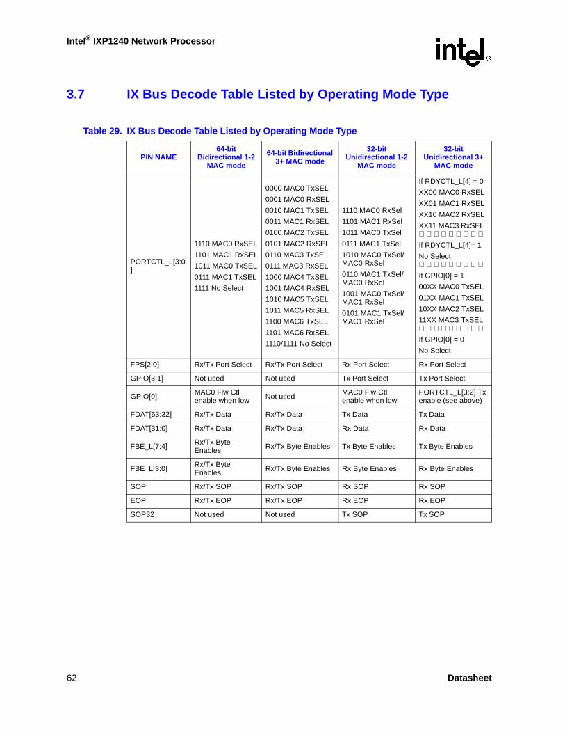
Intel® IXP1240 Network Processor
3.7 IX Bus Decode Table Listed by Operating Mode Type
Table 29. IX Bus Decode Table Listed by Operating Mode Type
PIN NAME64-bit
Bidirectional 1-2 MAC mode
64-bit Bidirectional 3+ MAC mode
32-bit Unidirectional 1-2
MAC mode
32-bit Unidirectional 3+
MAC mode
PORTCTL_L[3:0]
1110 MAC0 RxSEL
1101 MAC1 RxSEL
1011 MAC0 TxSEL
0111 MAC1 TxSEL
1111 No Select
0000 MAC0 TxSEL
0001 MAC0 RxSEL
0010 MAC1 TxSEL
0011 MAC1 RxSEL
0100 MAC2 TxSEL
0101 MAC2 RxSEL
0110 MAC3 TxSEL
0111 MAC3 RxSEL
1000 MAC4 TxSEL
1001 MAC4 RxSEL
1010 MAC5 TxSEL
1011 MAC5 RxSEL
1100 MAC6 TxSEL
1101 MAC6 RxSEL
1110/1111 No Select
1110 MAC0 RxSel
1101 MAC1 RxSel
1011 MAC0 TxSel
0111 MAC1 TxSel
1010 MAC0 TxSel/ MAC0 RxSel
0110 MAC1 TxSel/ MAC0 RxSel
1001 MAC0 TxSel/ MAC1 RxSel
0101 MAC1 TxSel/ MAC1 RxSel
If RDYCTL_L[4] = 0
XX00 MAC0 RxSEL
XX01 MAC1 RxSEL
XX10 MAC2 RxSEL
XX11 MAC3 RxSELIf RDYCTL_L[4]= 1
No SelectIf GPIO[0] = 1
00XX MAC0 TxSEL
01XX MAC1 TxSEL
10XX MAC2 TxSEL
11XX MAC3 TxSELIf GPIO[0] = 0
No Select
FPS[2:0] Rx/Tx Port Select Rx/Tx Port Select Rx Port Select Rx Port Select
GPIO[3:1] Not used Not used Tx Port Select Tx Port Select
GPIO[0] MAC0 Flw Ctl enable when low Not used MAC0 Flw Ctl
enable when lowPORTCTL_L[3:2] Tx enable (see above)
FDAT[63:32] Rx/Tx Data Rx/Tx Data Tx Data Tx Data
FDAT[31:0] Rx/Tx Data Rx/Tx Data Rx Data Rx Data
FBE_L[7:4] Rx/Tx Byte Enables Rx/Tx Byte Enables Tx Byte Enables Tx Byte Enables
FBE_L[3:0] Rx/Tx Byte Enables Rx/Tx Byte Enables Rx Byte Enables Rx Byte Enables
SOP Rx/Tx SOP Rx/Tx SOP Rx SOP Rx SOP
EOP Rx/Tx EOP Rx/Tx EOP Rx EOP Rx EOP
SOP32 Not used Not used Tx SOP Tx SOP
62 Datasheet

Intel® IXP1240 Network Processor
EOP Not used Not used Tx EOP Tx EOP
RDYCTL_L[4] MAC1 Flw Ctl enable when low
Ready Control (see below)
MAC1 Flw Ctl enable when low
PORTCTL_L[1:0] Rx enable (see above)
RDYCTL_L[4:0]
x1111 NOP
x1110 MAC0 Rx
x1101 MAC0 Tx
x1011 MAC1 Rx
x0111 MAC1 Tx
11111 NOP
11110 GET 1
11100 autopush
11011 MAC0 Rx
11010 MAC1 Rx
11001 MAC2 Rx
11000 MAC3 Rx
10111 MAC0 Tx
10110 MAC1 Tx
10101 MAC2 Tx
10100 MAC3 Tx
10011 MAC0 Flw Ctl enable
10010 MAC1 Flw Ctl enable
10001 MAC2 Flw Ctl enable
10000 MAC3 Flw Ctl enable
01110 GET 2
01101 SEND
01011 MAC4 Rx
01010 MAC5 Rx
01001 MAC6 Rx
00111 MAC4 Tx
00110 MAC5 Tx
00101 MAC6 Tx
00011 MAC4 Flw Ctl enable
00010 MAC5 Flw Ctl enable
00001 MAC6 Flw Ctl enable
x1111 NOP
x1110 MAC0 Rx
x1101 MAC0 Tx
x1011 MAC1 Rx
x0111 MAC1 Tx
x1111 NOP
x1110 GET 1
x1101 SEND
x1100 autopush
x1011 MAC0 Rx
x1010 MAC1 Rx
x1001 MAC2 Rx
x1000 MAC3 Rx
x0111 MAC0 Tx
x0110 MAC1 Tx
x0101 MAC2 Tx
x0100 MAC3 Tx
x0011 MAC0 Flw Ctl enable
x0010 MAC1 Flw Ctl enable
x0001 MAC2 Flw Ctl enable
x0000 MAC3 Flw Ctl enable
Table 29. IX Bus Decode Table Listed by Operating Mode Type (Continued)
PIN NAME64-bit
Bidirectional 1-2 MAC mode
64-bit Bidirectional 3+ MAC mode
32-bit Unidirectional 1-2
MAC mode
32-bit Unidirectional 3+
MAC mode
Datasheet 63

Intel® IXP1240 Network Processor
3.8 Pin State During Reset
Table 30 summarizes IXP1240 pin states during reset.
Table 30. Pin State During Reset
Function Pin Name Pin Reset State Comment
SRAM SCLK output, low
SRAM A[17:0] output, low
SRAM DQ[31:0] output, low
SRAM CE_L[3:0] output, high
SRAM SLOW_EN_L output, high
SRAM SOE_L output, high
SRAM SWE_L output, high
SRAM HIGH_EN_L output, high
SRAM LOW_EN_L output, high
SRAM MRD_L output, high
SRAM MCE_L output, high
SRAM FWE_L output, high
SRAM NA/SACLK input
SDRAM SDCLK active clock output
SDRAM MADR[14:0] output, low
SDRAM MDATA[63:0] output, low
SDRAM CAS_L output, high
SDRAM DQM output, high
SDRAM RAS_L output, high
SDRAM WE_L output, high
PCI PCI_CLK input
PCI AD[31:0]
PCI_CFN[1:0]=00, AD[31:0]=Hi-Z
PCI_CFN[1:0]=11 AD[31:0]=output, low
PCI CBE_L[3:0]
PCI_CFN[1:0]=00, CBE_L[[3:0]=Hi-Z
PCI_CFN[1:0]=11 CBE_L[3:0]=output, low
PCI FRAME_L Hi-Z
PCI PAR
PCI_CFN[1:0]=00, PAR=Hi-Z
PCI_CFN[1:0]=11 PAR=output, low
PCI IDSEL Hi-Z
PCI PCI_CFN[0] input
PCI PCI_CFN[1] input
64 Datasheet

Intel® IXP1240 Network Processor
PCI PCI_IRQ_L Hi-Z
PCI PCI_RST_L
PCI_CFN[1:0]=00, PCI_RST=Hi-Z
PCI_CFN[1:0]=11, PCI_RST=output, low
PCI PERR_L Hi-Z
PCI SERR_L Hi-Z
PCI STOP_L Hi-Z
PCI DEVSEL_L Hi-Z
PCI TRDY_L Hi-Z
PCI GNT_L[1:0]
PCI_CFN[1:0]=00, GNT_L[1:0]=Hi-Z
PCI_CFN[1:0]=11, GNT_L[1:0]=output, high
PCI REQ_L[1:0] Hi-Z
IX Bus FCLK input
IX Bus FDAT[63:0] output, high
IX Bus FBE_L[7:4] output, high
IX Bus FBE_L[3:0] output, high
IX Bus FPS[2:0] output, high
IX Bus TXASIS output, high
IX Bus PORTCTL_L[3:0] output, high
IX Bus FAST_RX1 input
IX Bus FAST_RX2 input
IX Bus RDYBUS[7:0] output, high
IX Bus RDYCTL_L[3:0] output, high
IX Bus RDYCTL_L[4] output, high
IX Bus EOP output, high
IX Bus SOP output, high
IX Bus EOP32 output, high
IX Bus SOP32 output, high
IX Bus RXFAIL output, high
IX Bus TK_IN input drive or pullup high to select initial owner
IX Bus TK_OUT Hi-Z
IX Bus GPIO[3] input
IX Bus GPIO[2] input
IX Bus GPIO[1] input
IX Bus GPIO[0] input
Misc Test TCK_BYP input
Table 30. Pin State During Reset (Continued)
Function Pin Name Pin Reset State Comment
Datasheet 65

Intel® IXP1240 Network Processor
3.9 Pullup/Pulldown and Unused Pin Guidelines
For normal (i.e., non-test mode) operation, terminate signals as follows:
• Pullup these signals to VDDX: TMS, TDI.
• TCK may be pulled up to VDDX or pulled down to VSSX at the system designer’s option.
• Pulldown these signals to VSS: SCAN_EN, TCK_BYP, TRST_L.
• Pullup this signal to VDDX or pulldown to VSS; do not allow it to float: TSTCLK.
• GPIO[3:1] and GPIO[0] are tri-stated during reset. If these signals are used to drive external logic, pullup or pulldown as approprate to ensure valid logic levels during reset.
Terminate unused signals as follows:
• Pullup these signals to VDDX: GNT_L[1], TK_IN, EOP32.
• Pulldown these signals to VSS: NA/SACLK, FAST_RX1, FAST_RX2.
For shared IX Bus operation, it is recommended to pullup PORTCTL_L[3:0] and, additionally, FPS[2:0] and TXASIS at the designer’s discretion.
Typical pullup/pulldown resistor values are in the range of 5-10 KOhms.
Misc Test TSTCLK input
Misc Test SCAN_EN input
Processor Support PXTAL input
Processor Support CINT_L input
Processor Support RESET_IN_L input
Processor Support RESET_OUT_L output, low
Serial RXD input
Serial TXD output, high
IEEE 1149.1 TCK input
IEEE 1149.1 TDI input
IEEE 1149.1 TDO output, undefined
IEEE 1149.1 TMS input
IEEE 1149.1 TRST_L input
Table 30. Pin State During Reset (Continued)
Function Pin Name Pin Reset State Comment
66 Datasheet

Intel® IXP1240 Network Processor
4.0 Electrical Specifications
This chapter specifies the following electrical behavior of the IXP1240:
• Absolute maximum ratings.
• DC specifications.
• AC timing specifications for the following signal interfaces:
— PXTAL Clock input.
— PCI Bus Interface.
— IX Bus Interface.
— Ready Bus Interface.
— TK_OUT/TK_IN signals.
— SRAM interface.
— SDRAM Interface.
— Reset signals.
— GPIO signals.
— IEEE 1149.1 Interface.
— Serial Port signals.
4.1 Absolute Maximum Ratings
The IXP1240 is specified to operate at a maximum core frequency (Fcore) of 232 MHz at a junction temperature (Tj) not to exceed 100°C. Table 31 lists the absolute maximum ratings for the IXP1240. These are stress ratings only; stressing the device beyond the absolute maximum ratings may cause permanent damage. Operating beyond the functional operating range (Table 31) is not recommended and extended exposure beyond the functional operating range may affect reliability.
Under all operating conditions, the 3.3 V to 2.0 V supply voltage difference (Vdelta) must not be exceeded or permanent damage to the device may result.
Table 31. Absolute Maximum Ratings
Parameter Minimum Maximum Comment
Junction temperature, Tj --- 100°C
Maximum voltage applied to signal pins 3.6 V
Supply voltage (core and PLL), VDD, VDDP1 1.9 V 2.1 V 2 V supply
Supply voltage (I/O), VDDX, VDDREF 3.0 V 3.6 V 3.3 V supply
Storage temperature range -55°C 125°C
Vdelta 0.0 V 1.8 V (VDDX - VDD) or(VDDX - VDDP1)
Datasheet 67

Intel® IXP1240 Network Processor
The power specifications listed below are based on the following assumption:
• PCI Bus Frequency (PCI_CLK) = 66 MHz.
Table 32. Functional Operating Range
Parameter Minimum Maximum Comment
Operating temperature range 0°C 70°C
Tjmax to be managed to stay below 100°C. (see the Heatsink application in Figure 12).
Supply voltage (core and PLL), VDD, VDDP1 1.9 V 2.1 V 2.0 V +/- 5%
Supply voltage (I/O), VDDX, VDDREF 3.0 V 3.6 V 3.3 V +/- 10%
Table 33. Typical and Maximum Power
Parameter
Core Freq/IX Bus Freq166 MHz/66 MHz
Core Freq/IX Bus Freq200 MHz/85 MHz
Core Freq/IX Bus Freq232 MHz/104 MHz
Typical1,2
1. Typical and maximum power specifications are based upon the bus loading shown in Table 34.2. Typical power measured at nominal supply voltages.
Maximum1 Typical1,2 Maximum1 Typical1,2 Maximum1
2.0 V supply 3.3 W 4.8 W 3.9 W 5.4 W 4.5 W 5.9 W
3.3 V supply 0.5 W 1.2 W 0.58 W 1.2 W 0.69 W 0.8 W
Total Power 3.80 W 6.0 W 4.48 W 6.6 W 5.19 W 6.7 W
Table 34. Maximum and Typical Bus Loading Used for the Power Calculations1
1. A load is defined as input capacitance equivalent to a CMOS gate + minimal trace length capacitance, typically 8 pF. Thecustomer is responsible for managing the signal integrity and external power issues that occur with increased IXP1240 Busloading in their application to ensure reliable system operation.
Maximum Power Load for
Core Freq/IX Bus Freq
166 MHz/66 MHz
Maximum Power Load for
Core Freq/IX Bus Freq
200 MHz/85 MHz
Maximum Power Load for
Core Freq/IX Bus Freq
232 MHz/104 MHz
Typical Power Load for IX Bus Frequency ≤ 85 MHz
SDRAM Bus 8 8 5 5
SRAM Bus 8 8 5 5
IX Bus 7 4 1 2
68 Datasheet

Intel® IXP1240 Network Processor
Note: Refer to the IXP1200 Network Processor Heatsinks: θja and Airflow - Application Note for additional information on heatsinks and thermal management.
Figure 12. Typical IXP1240 Heatsink Application
A8541-01
12.5
10.0
7.5
5.0
2.50 100 200 300 400 500 600 700 800
Airflow (LFM)
/ ja(
˚c/w
)
Bare Package
HST354HST355Fan HS
HST353
Datasheet 69
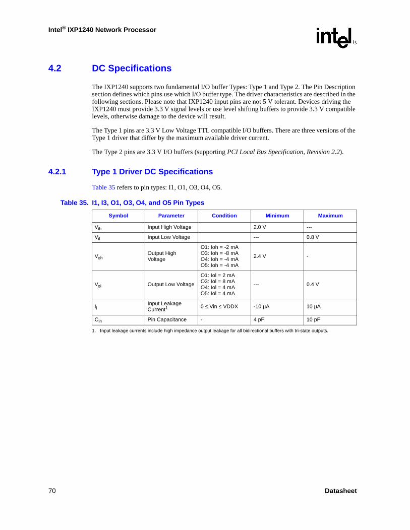
Intel® IXP1240 Network Processor
4.2 DC Specifications
The IXP1240 supports two fundamental I/O buffer Types: Type 1 and Type 2. The Pin Description section defines which pins use which I/O buffer type. The driver characteristics are described in the following sections. Please note that IXP1240 input pins are not 5 V tolerant. Devices driving the IXP1240 must provide 3.3 V signal levels or use level shifting buffers to provide 3.3 V compatible levels, otherwise damage to the device will result.
The Type 1 pins are 3.3 V Low Voltage TTL compatible I/O buffers. There are three versions of the Type 1 driver that differ by the maximum available driver current.
The Type 2 pins are 3.3 V I/O buffers (supporting PCI Local Bus Specification, Revision 2.2).
4.2.1 Type 1 Driver DC Specifications
Table 35 refers to pin types: I1, O1, O3, O4, O5.
Table 35. I1, I3, O1, O3, O4, and O5 Pin Types
Symbol Parameter Condition Minimum Maximum
Vih Input High Voltage 2.0 V ---
Vil Input Low Voltage --- 0.8 V
VohOutput High Voltage
O1: Ioh = -2 mAO3: Ioh = -8 mAO4: Ioh = -4 mAO5: Ioh = -4 mA
2.4 V -
Vol Output Low Voltage
O1: Iol = 2 mAO3: Iol = 8 mAO4: Iol = 4 mAO5: Iol = 4 mA
--- 0.4 V
IiInput Leakage Current1
1. Input leakage currents include high impedance output leakage for all bidirectional buffers with tri-state outputs.
0 ≤ Vin ≤ VDDX -10 µA 10 µA
Cin Pin Capacitance - 4 pF 10 pF
70 Datasheet
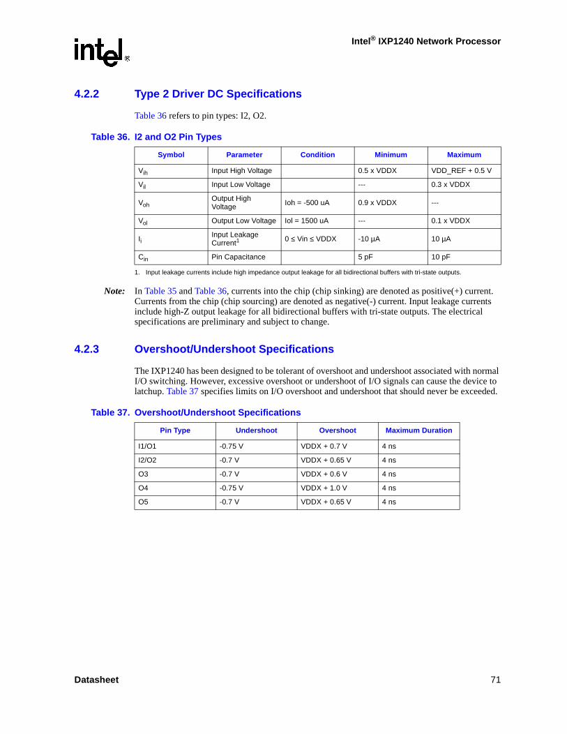
Intel® IXP1240 Network Processor
4.2.2 Type 2 Driver DC Specifications
Table 36 refers to pin types: I2, O2.
Note: In Table 35 and Table 36, currents into the chip (chip sinking) are denoted as positive(+) current. Currents from the chip (chip sourcing) are denoted as negative(-) current. Input leakage currents include high-Z output leakage for all bidirectional buffers with tri-state outputs. The electrical specifications are preliminary and subject to change.
4.2.3 Overshoot/Undershoot Specifications
The IXP1240 has been designed to be tolerant of overshoot and undershoot associated with normal I/O switching. However, excessive overshoot or undershoot of I/O signals can cause the device to latchup. Table 37 specifies limits on I/O overshoot and undershoot that should never be exceeded.
Table 36. I2 and O2 Pin Types
Symbol Parameter Condition Minimum Maximum
Vih Input High Voltage 0.5 x VDDX VDD_REF + 0.5 V
Vil Input Low Voltage --- 0.3 x VDDX
VohOutput High Voltage Ioh = -500 uA 0.9 x VDDX ---
Vol Output Low Voltage Iol = 1500 uA --- 0.1 x VDDX
IiInput Leakage Current1
1. Input leakage currents include high impedance output leakage for all bidirectional buffers with tri-state outputs.
0 ≤ Vin ≤ VDDX -10 µA 10 µA
Cin Pin Capacitance 5 pF 10 pF
Table 37. Overshoot/Undershoot Specifications
Pin Type Undershoot Overshoot Maximum Duration
I1/O1 -0.75 V VDDX + 0.7 V 4 ns
I2/O2 -0.7 V VDDX + 0.65 V 4 ns
O3 -0.7 V VDDX + 0.6 V 4 ns
O4 -0.75 V VDDX + 1.0 V 4 ns
O5 -0.7 V VDDX + 0.65 V 4 ns
Datasheet 71

Intel® IXP1240 Network Processor
4.3 AC Specifications
4.3.1 Clock Timing Specifications
The ac specifications consist of input requirements and output responses. The input requirements consist of setup and hold times, pulse widths, and high and low times. Output responses are delays from clock to signal. The ac specifications are defined separately for each clock domain within the IXP1240.
For example, Figure 14 shows the ac parameter measurements for the PCI_CLK signal, and Table 39 and Table 40 specify parameter values for clock signal ac timing. See also Figure 15 for a further illustration of signal timing. Unless otherwise noted, all ac parameters are guaranteed when tested within the functional operating range of Table 32.
Unless otherwise indicated, all ac output delays are measured with a 5 pF load. Capacitive deratings are provided for all output buffers.
4.3.2 PXTAL Clock Input
Figure 13. PXTAL Clock Input
Table 38. PXTAL Clock Inputs
Symbol Parameter Minimum Typical Maximum Unit
Fpxtal Clock frequency 3.5795 3.6864 3.7878 MHz
Vptp Clock peak to peak 0.6*VDDX --- V
Vhigh Clock high threshold 2.0 --- V
Vlow Clock low threshold --- 0.8 V
Clock slew rate1
1. Not tested. Guaranteed by design.
1 4 V/ns
Fcore Core frequency2,3,4
2. Core frequency (Fcore) of 165.89 MHz when register PLL_CFG[4:0] = 10000b.3. Core frequency (Fcore) of 166.67 MHz when register PLL_CFG[4:0] = 01111b and Fpxtal = 3.7878 MHz. Refer to the IXP1200
Network Processor Family Microcode Programmer’s Reference Manual for a complete list of programmable frequencies.4. Core frequency (Fcore) of 199.0656 MHz when register PLL_CFG[4:0] = 10011b and Fpxtal = 3.6864 MHz. Refer to the IXP1200
Network Processor Family Microcode Programmer’s Reference Manual for a complete list of programmable frequencies.
165.89 MHz
A8553-01
1/FPXTAL
TfTr
Vl
Vh
Vptp
Thigh
Tlow
72 Datasheet
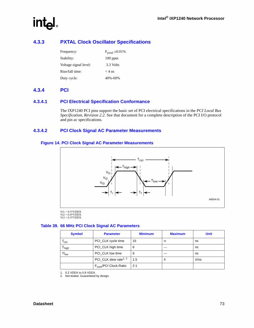
Intel® IXP1240 Network Processor
4.3.3 PXTAL Clock Oscillator Specifications
Frequency: Fpxtal ±0.01%
Stability: 100 ppm
Voltage signal level: 3.3 Volts
Rise/fall time: < 4 ns
Duty cycle: 40%-60%
4.3.4 PCI
4.3.4.1 PCI Electrical Specification Conformance
The IXP1240 PCI pins support the basic set of PCI electrical specifications in the PCI Local Bus Specification, Revision 2.2. See that document for a complete description of the PCI I/O protocol and pin ac specifications.
4.3.4.2 PCI Clock Signal AC Parameter Measurements
Vt1 = 0.5*VDDXVt2 = 0.4*VDDXVt3 = 0.3*VDDX
Figure 14. PCI Clock Signal AC Parameter Measurements
A8554-01
Tcyc
TfTr
Vt3
Vt1
Vt2
Thigh
Tlow
Table 39. 66 MHz PCI Clock Signal AC Parameters
Symbol Parameter Minimum Maximum Unit
Tcyc PCI_CLK cycle time 15 ∞ ns
Thigh PCI_CLK high time 6 --- ns
Tlow PCI_CLK low time 6 --- ns
PCI_CLK slew rate1, 2
1. 0.2 VDDX to 0.6 VDDX.2. Not tested. Guaranteed by design.
1.5 4 V/ns
Fcore/PCI Clock Ratio 2:1
Datasheet 73

Intel® IXP1240 Network Processor
Table 40. 33 MHz PCI Clock Signal AC Parameters
Symbol Parameter Minimum Maximum Unit
Tcyc PCI_CLK cycle time 30 ∞ ns
Thigh PCI_CLK high time 11 --- ns
Tlow PCI_CLK low time 11 --- ns
PCI_CLK slew rate1 2
1. 0.2 VDDX to 0.6 VDDX.2. Not tested. Guaranteed by design.
1 4 V/ns
Fcore/PCI Clock Ratio 2:1
Figure 15. PCI Bus Signals
A8555-01
Tval(max)
Tsu Th
Tval(min)
Ton Toff
VtestPCI_CLK
Outputs
Inputs
Note: Vtest = 0.4 VDDX for 3.3 volt PCI signals
74 Datasheet
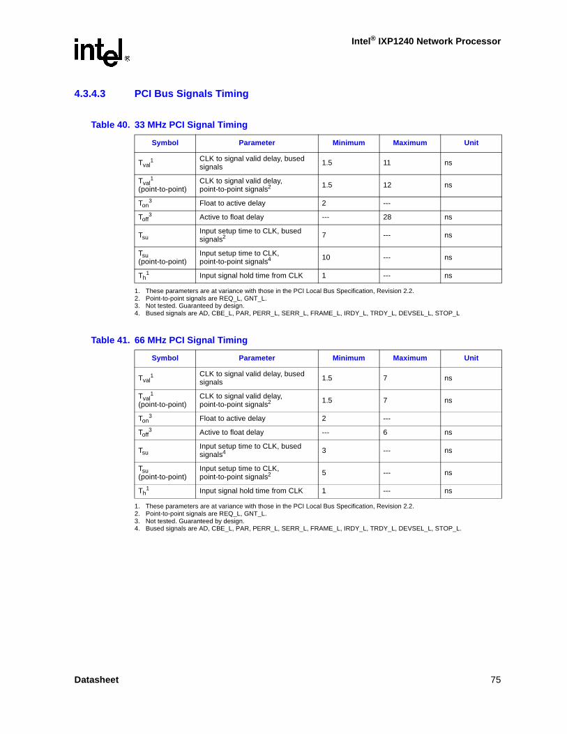
Intel® IXP1240 Network Processor
4.3.4.3 PCI Bus Signals Timing
Table 40. 33 MHz PCI Signal Timing
Symbol Parameter Minimum Maximum Unit
Tval1
1. These parameters are at variance with those in the PCI Local Bus Specification, Revision 2.2.
CLK to signal valid delay, bused signals 1.5 11 ns
Tval1
(point-to-point)CLK to signal valid delay, point-to-point signals2
2. Point-to-point signals are REQ_L, GNT_L.
1.5 12 ns
Ton3
3. Not tested. Guaranteed by design.
Float to active delay 2 ---
Toff3 Active to float delay --- 28 ns
TsuInput setup time to CLK, bused signals2 7 --- ns
Tsu (point-to-point)
Input setup time to CLK, point-to-point signals4
4. Bused signals are AD, CBE_L, PAR, PERR_L, SERR_L, FRAME_L, IRDY_L, TRDY_L, DEVSEL_L, STOP_L
10 --- ns
Th1 Input signal hold time from CLK 1 --- ns
Table 41. 66 MHz PCI Signal Timing
Symbol Parameter Minimum Maximum Unit
Tval1
1. These parameters are at variance with those in the PCI Local Bus Specification, Revision 2.2.
CLK to signal valid delay, bused signals 1.5 7 ns
Tval1
(point-to-point)CLK to signal valid delay, point-to-point signals2
2. Point-to-point signals are REQ_L, GNT_L.
1.5 7 ns
Ton3
3. Not tested. Guaranteed by design.
Float to active delay 2 ---
Toff3 Active to float delay --- 6 ns
TsuInput setup time to CLK, bused signals4
4. Bused signals are AD, CBE_L, PAR, PERR_L, SERR_L, FRAME_L, IRDY_L, TRDY_L, DEVSEL_L, STOP_L.
3 --- ns
Tsu (point-to-point)
Input setup time to CLK, point-to-point signals2 5 --- ns
Th1 Input signal hold time from CLK 1 --- ns
Datasheet 75

Intel® IXP1240 Network Processor
4.3.5 Reset
4.3.5.1 Reset Timings Specification
Table 42 shows the reset timing specifications for RESET_IN_L and RESET_OUT_L.
Table 42. Reset Timings Specification
Symbol Parameter Minimum Maximum Unit
tRSTRESET_IN_L asserted after power stable. 150 -- ms
tSG GPIO[3] setup to reset sample edge. 2 core_clk cycles1
1. core_clk is nominally running at 29.491 MHz after a hard reset when PXTAL is 3.6864 MHz.
tHGGPIO[3] hold from reset sample edge. 9 core_clk cycles1
tOETK TK_OUT hi-z to valid output. 4 7 core_clk cycles1
Figure 16. RESET_IN_L Timing Diagram
A8876-01
VDD: VDDX, VDDP,VDD_REF
RESET_IN_L
sram_rst_1[note 1]
tRST
tsg
GPIO<3>
TK_OUT
509 PXTALCycles
Valid
tng
toetk
Note 1: Internal signal to the Intel® IXP1240 processor.
76 Datasheet
Intel® IXP1240 Network Processor
4.3.6 IEEE 1149.1
The following pins are considered IEEE 1149.1 compliance pins:RESET_IN_LPCI_CLKSCAN_ENTCK_BYPTSTCLK
The following pins are not connected to the Boundary Scan ring:RESET_IN_LPCI_CLKSCAN_ENTCK_BYPTSTCLKTCKTMSTDITDOTRST_L
Caution: A clock signal must be applied to the core of the IXP1240 when using IEEE 1149.1 functions. The PXTAL clock input should be active, or, if using bypass mode, (TCK_BYP = 1) TSTCLK should be active. Failure to observe this rule may cause device damage.
Datasheet 77

Intel® IXP1240 Network Processor
4.3.6.1 IEEE 1149.1 Timing Specifications
Figure 17. IEEE 1149.1/Boundary-Scan General Timing
A8557-01
tck
Data In
Data Out
tdo
tms, tdi
Tbscl Tbsch
Tbsis
Tbsih
Tbsoh
Tbsod
Tbsss
Tbssh
Tbsdh
Tbsdd
78 Datasheet

Intel® IXP1240 Network Processor
Table 43 shows the IEEE 1149.1/boundary-scan interface timing specifications.
Figure 18. IEEE 1149.1/Boundary-Scan Tri-State Timing
A8558-01
tck
Data Out
tdo
Tbsoe Tbsoz
Tbsde Tbsdz
Table 43. IEEE 1149.1/Boundary-Scan Interface Timing
Symbol Parameter Minimum Typical Maximum Units Notes
Freq TCK frequency 10 MHz
Tbscl TCK low period – 50 – ns 1
Tbsch TCK high period – 50 – ns 1
Tbsis TDI,TMS setup time 40 – – ns –
Tbsih TDI,TMS hold time 40 – – ns –
Tbsod TDO valid delay 20 – 30 ns –
Tbsss I/O signal setup time 40 – – ns –
Tbssh I/O signal hold time 40 – – ns –
Tbsdd Data output valid 20 – 30 ns –
Tbsoe1,Tbsoz
1 TDO float delay 5 – 40 ns –
Tbsde1, Tbsdz
1 Data output float delay 5 – 40 ns –
Tbsr Reset period 40 – – ns –
NOTES:1. TCK may be stopped indefinitely in either the low or high phase.
1. Not tested. Guaranteed by design.
Datasheet 79

Intel® IXP1240 Network Processor
4.3.7 IX Bus
4.3.7.1 FCLK Signal AC Parameter Measurements
Figure 19. FCLK Signal AC Parameter Measurements
Table 44. FCLK Signal AC Parameter Measurements
Symbol Parameter Minimum Maximum Unit
FCLK Clock frequency 10 1041
1. Maximum FCLK frequency for 232 MHz rated parts is 104 MHz. Maximum FCLK frequency for 200 MHz rated parts is 85 MHz.Maximum FCLK frequency for 166 MHz rated parts is 66 MHz.
MHz
Tc Cycle time 9.621 100 ns
Thigh2
2. Thigh and Tlow are based on a 50% duty cycle and can vary (worst case) 45-55%.
Clock high time 3.8 --- ns
Tlow2 Clock low time 3.8 --- ns
Vptp Clock peak to peak2 0.6*VDDX --- V
Tr, Tf Clock rise/fall time3
3. Nominal Vptp = 0.12*VDDX to 0.75*VDDX.
1 4 ns
Fcore/FCLK Clock Ratio 1.5:1
A8573-01
Tc
TfTr
Vl
Vh
Vptp
Thigh
Tlow
80 Datasheet
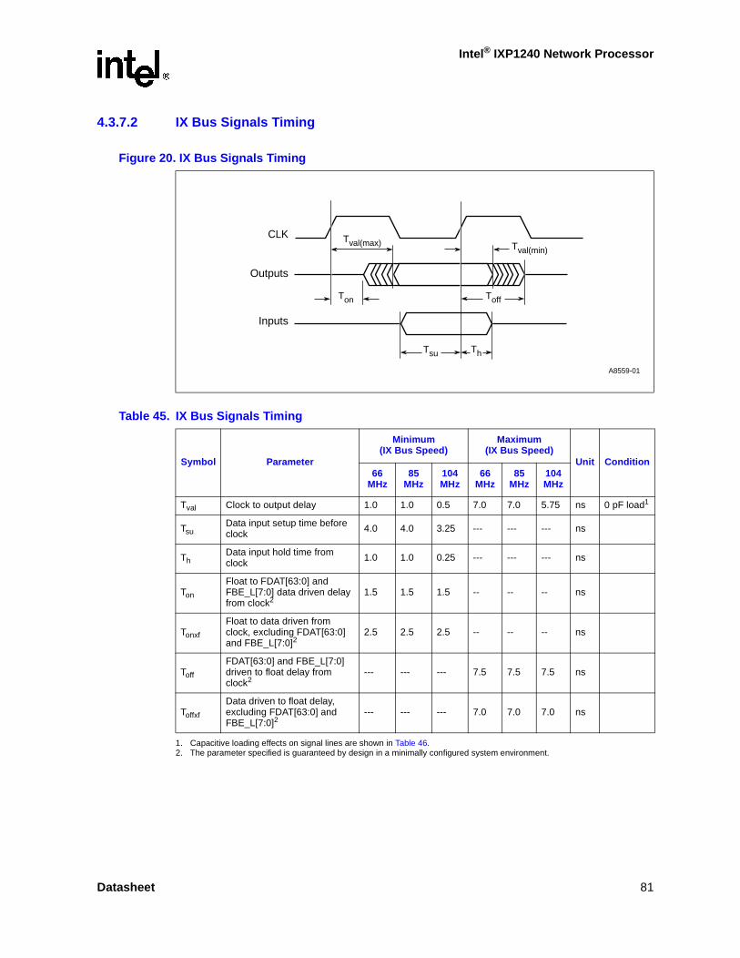
Intel® IXP1240 Network Processor
4.3.7.2 IX Bus Signals Timing
Figure 20. IX Bus Signals Timing
Table 45. IX Bus Signals Timing
Symbol Parameter
Minimum(IX Bus Speed)
Maximum(IX Bus Speed)
Unit Condition66
MHz85
MHz104MHz
66MHz
85MHz
104MHz
Tval Clock to output delay 1.0 1.0 0.5 7.0 7.0 5.75 ns 0 pF load1
1. Capacitive loading effects on signal lines are shown in Table 46.
TsuData input setup time before clock 4.0 4.0 3.25 --- --- --- ns
ThData input hold time from clock 1.0 1.0 0.25 --- --- --- ns
Ton
Float to FDAT[63:0] and FBE_L[7:0] data driven delay from clock2
2. The parameter specified is guaranteed by design in a minimally configured system environment.
1.5 1.5 1.5 -- -- -- ns
Tonxf
Float to data driven from clock, excluding FDAT[63:0] and FBE_L[7:0]2
2.5 2.5 2.5 -- -- -- ns
Toff
FDAT[63:0] and FBE_L[7:0] driven to float delay from clock2
--- --- --- 7.5 7.5 7.5 ns
Toffxf
Data driven to float delay, excluding FDAT[63:0] and FBE_L[7:0]2
--- --- --- 7.0 7.0 7.0 ns
A8559-01
Tval(max)
Tsu Th
Tval(min)
Ton Toff
CLK
Outputs
Inputs
Datasheet 81

Intel® IXP1240 Network Processor
Table 46. Signal Delay Derating
Signal Maximum Derating (ns/pF) Minimum Derating (ns/pF)
66 MHz 85 MHz 104 MHz 66 MHz 85 MHz 104 MHz
FDATA[63:0] 0.055 0.05 0.031 0.03 0.025 0.015
FBE_L[7:0] 0.055 0.05 0.031 0.03 0.025 0.015
FPS[2:0] 0.065 0.06 0.031 0.03 0.025 0.015
TK_REQ_OUT 0.065 0.06 0.031 0.03 0.025 0.015
TK_REQ_IN 0.065 0.06 0.031 0.03 0.025 0.015
RDYCTL_L[4:0] 0.065 0.06 0.031 0.03 0.025 0.015
RDYBUS[7:0] 0.065 0.06 0.031 0.03 0.025 0.015
TXAXIS 0.065 0.06 0.031 0.03 0.025 0.015
EOP 0.065 0.06 0.031 0.03 0.025 0.015
SOP 0.065 0.06 0.031 0.03 0.025 0.015
GPIO[3:0] 0.065 0.06 0.031 0.03 0.025 0.015
PORTCTL_L[3:0] 0.095 0.09 0.035 0.03 0.025 0.015
TK_OUT 0.095 0.09 0.035 0.03 0.025 0.015
RXFAIL 0.095 0.09 0.035 0.03 0.025 0.015
82 Datasheet

Intel ® IX
P1240 N
etwo
rk Pro
cessor
Datash
eet83
4.3.7.3IX
Bu
s Pro
toco
l
The follow
ing timing diagram
s show the IX
Bus signal protocol for both 64-bit B
idirectional and 32-bit U
nidirectional modes of operation.
Fig
ure 21. 64-B
it Bid
irection
al IX B
us Tim
ing
, 1-2 MA
C M
od
e, Co
nsecu
tive Receive an
d
Transm
it, No
EO
P
/Tx D
t D
Td7Td6Td5Td4
A8908-01
FCLK
PORTCTL_L[0]
PORTCTL_L[1]
PORTCTL_L[2]
PORTCTL_L[3]
FPS[2:0]
FDAT[63:0]
SOP
EOP
FBE_L[7:0]
int_1240_OE
MAC0/Rx A
MAC0/Tx B
MAC1/Rx C
MAC1
Notes:int_1240_OE is not an Intel® IXP1240 Processor signal. It is shown to indicate when the IXP1240 drives the FDATx,FBE_Lx, SOP, EOP, TXAXIS, SOP32, EOP32 pins.
Status Command indicated with STS-A, STS-B, etc.Status Data Transfer indicated with RaS, RbS, RcS, etc.
Port CPort BPort A Por
Td3Td2Td1Td0Rc7Rc6Rc5Rc4Rc3Rc2Rc1Rc0Tb7Tb6Tb5Tb4Tb3Tb2Tb1Tb0Ra7Ra6Ra5Ra4Ra3Ra2Ra1Ra0

Intel ® IX
P1240 N
etwo
rk Pro
cessor
84 D
atasheet
Fig
ure 22. 64-B
it Bid
irection
al IX B
us Tim
ing
- Co
nsecu
tive Receive an
d Tran
smit, N
o E
OP
1240 drives the FDATx, FBE_Lx,
MAC1/Rx C
Port C
Rc1 Rc2 Rc3 Rc4Rc0
A8877-01
Notes:Signals using prefix "ext_" are outputs of an external decoder in 3+ MAC mode.
Status Command indicated with STS-A, STS-B, etc.Status Data Transfer indicated with RaS, RbS, RcS, etc.
int_1250_OE is not an Intel® IXP1240 Processor signal. It is shown to indicate when the IXPSOP/SOP_RX, EOP/EOP_RX, TXAXIS, SOP32, EOP32 pins.
FCLK
PORTCTL_L[3:0] MAC0/Rx A MAC1/Tx B
No Select
No Select
ext_MAC0_Rx_L
ext_MAC1_Tx_L
ext_MAC2_Rx_L
FPS[2:0] Port A Port B
FDAT[63:0] Ra0 Ra1 Ra2 Ra3 Ra4 Ra5 Ra6 Ra7 Tb0 Tb1 Tb2 Tb3 Tb4 Tb5 Tb6 Tb7
SOP
EOP
FBE_L[7:0]
int_1240_OE

Intel ® IX
P1240 N
etwo
rk Pro
cessor
Datash
eet85
Fig
ure 23. 64-B
it Bid
irection
al IX B
us T
imin
g - C
on
secutive R
eceive and
Transm
it, EO
P o
n 8th
D
ata Retu
rn w
ith S
tatus
40 drives the FDATx,
No Sel
STS-C
No Select D
Port C
rt D
2 Td3 Td6 Td7 RcS
A8878-01
FCLK
Notes:Signals using prefix "ext_" are outputs of an external decoder in 3+ MAC mode.
int_1240_OE is not an Intel® IXP1240 Processor signal. It is shown to indicate when the IXP12FBE_Lx, SOP, EOP, TXAXIS, SOP32, EOP32 pins.
Status Command indicated with STS-A, STS-B, etc.Status Data Transfer indicated with RaS, RbS, RcS, etc.
MAC1/Tx B
No Sel No Sel
STS-A
MAC2/Rx CPORTCTL_L[3:0] No SelectMAC0/Rx A No Select MAC2/Tx
ext_MAC0_Rx_L
ext_MAC1_Tx_L
ext_MAC2_Rx_L
ext_MAC3_Tx_L
Port A Port B Port C
Port A
PoFPS[2:0]
Td0 Td1 TdRc0 Rc1 Rc4 Rc5 Rc6 Rc7 RaSTb0 Tb1 Tb2 Tb3 Tb6 Tb7Ra0 Ra1FDAT[63:0] Ra4 Ra5 Ra6 Ra7
SOP
EOP
FBE_L[7:0]
Int_1240_OE
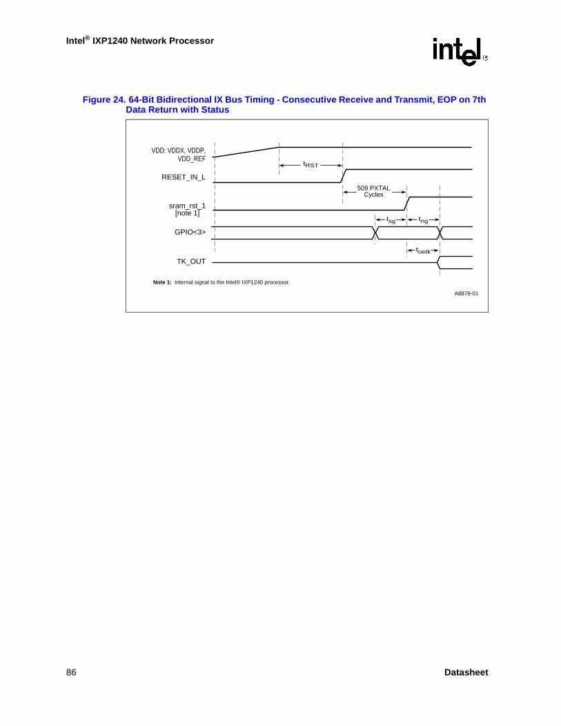
Intel® IXP1240 Network Processor
Figure 24. 64-Bit Bidirectional IX Bus Timing - Consecutive Receive and Transmit, EOP on 7th Data Return with Status
A8879-01
VDD: VDDX, VDDP,VDD_REF
RESET_IN_L
sram_rst_1[note 1]
tRST
tsg
GPIO<3>
TK_OUT
509 PXTALCycles
Valid
tng
toetk
Note 1: Internal signal to the Intel® IXP1240 processor.
86 Datasheet
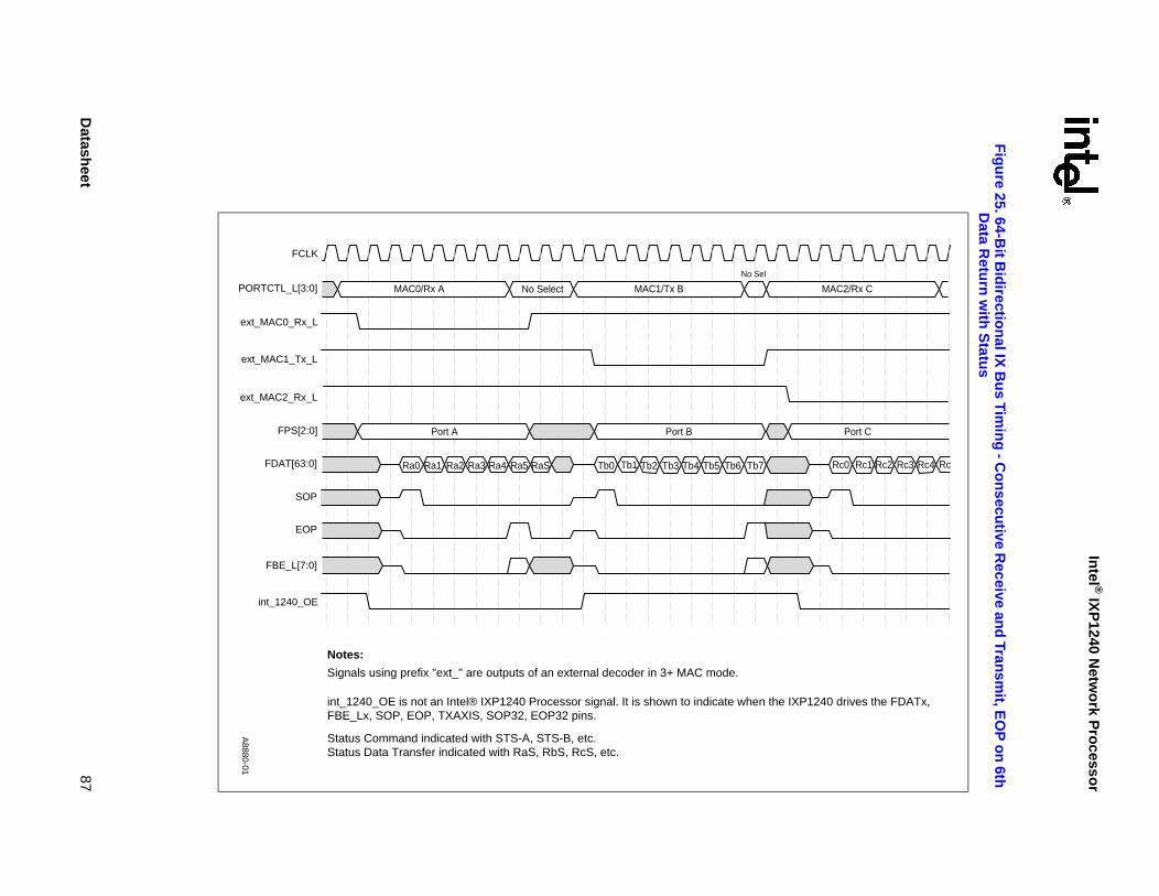
Intel ® IX
P1240 N
etwo
rk Pro
cessor
Datash
eet87
Fig
ure 25. 64-B
it Bid
irection
al IX B
us T
imin
g - C
on
secutive R
eceive and
Transm
it, EO
P o
n 6th
D
ata Retu
rn w
ith S
tatus
1240 drives the FDATx,
MAC2/Rx C
Port C
Rc0 Rc1 Rc2 Rc4 RcRc3
A8880-01
FCLK
Notes:
Signals using prefix "ext_" are outputs of an external decoder in 3+ MAC mode.
int_1240_OE is not an Intel® IXP1240 Processor signal. It is shown to indicate when the IXPFBE_Lx, SOP, EOP, TXAXIS, SOP32, EOP32 pins.
Status Command indicated with STS-A, STS-B, etc.Status Data Transfer indicated with RaS, RbS, RcS, etc.
PORTCTL_L[3:0] MAC0/Rx A MAC1/Tx B
No Sel
No Select
ext_MAC0_Rx_L
ext_MAC1_Tx_L
ext_MAC2_Rx_L
FPS[2:0] Port A Port B
FDAT[63:0] Ra0 Ra1 Ra2 Ra4 Ra5 RaSRa3 Tb0 Tb1 Tb2 Tb4 Tb5 Tb6 Tb7Tb3
SOP
EOP
FBE_L[7:0]
int_1240_OE
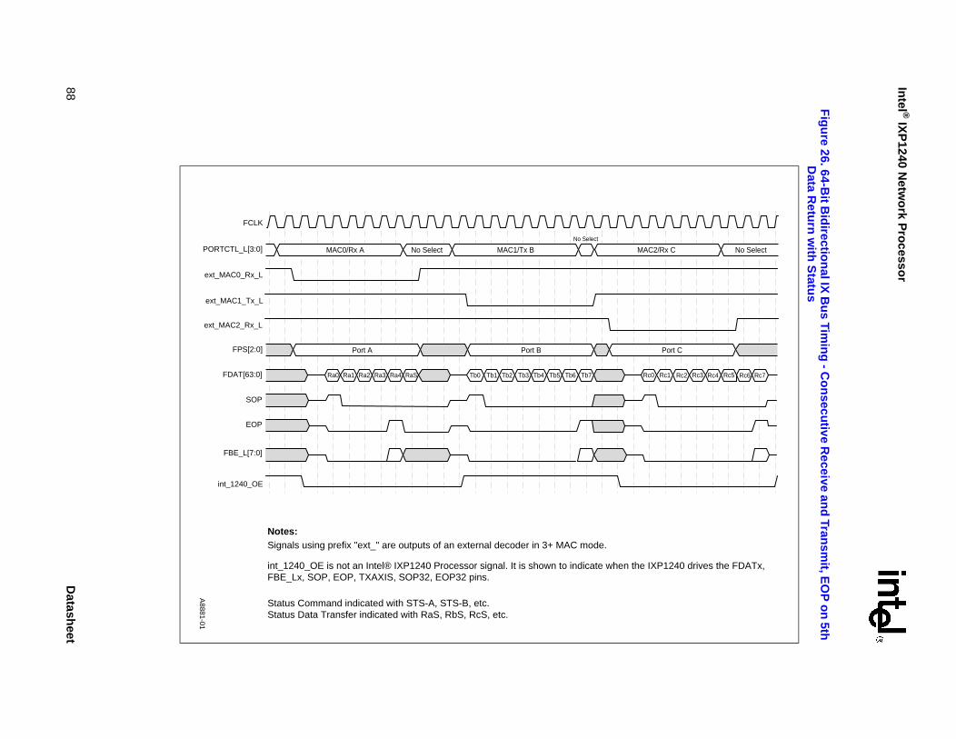
Intel ® IX
P1240 N
etwo
rk Pro
cessor
88 D
atasheet
Fig
ure 26. 64-B
it Bid
irection
al IX B
us Tim
ing
- Co
nsecu
tive Receive an
d Tran
smit, E
OP
on
5th
Data R
eturn
with
Statu
s
P1240 drives the FDATx,
/Rx C No Select
Port C
Rc1 Rc2 Rc3 Rc4 Rc5 Rc6 Rc7
A8881-01
FCLK
Notes:Signals using prefix "ext_" are outputs of an external decoder in 3+ MAC mode.
Status Command indicated with STS-A, STS-B, etc.Status Data Transfer indicated with RaS, RbS, RcS, etc.
int_1240_OE is not an Intel® IXP1240 Processor signal. It is shown to indicate when the IXFBE_Lx, SOP, EOP, TXAXIS, SOP32, EOP32 pins.
PORTCTL_L[3:0] MAC0/Rx A MAC1/Tx BNo Select
No Select
MAC2
ext_MAC0_Rx_L
ext_MAC1_Tx_L
ext_MAC2_Rx_L
FPS[2:0] Port A Port B
FDAT[63:0] Ra0 Ra1 Ra2 Ra3 Ra4 RaS Tb0 Tb1 Tb2 Tb3 Tb4 Tb5 Tb6 Rc0Tb7
SOP
EOP
FBE_L[7:0]
int_1240_OE

Intel ® IX
P1240 N
etwo
rk Pro
cessor
Datash
eet89
Fig
ure 27. 64-B
it Bid
irection
al IX B
us T
imin
g - C
on
secutive R
eceive and
Transm
it, EO
P o
n 4th
D
ata Retu
rn w
ith S
tatus
1240 drives the FDATx,
MAC2/Rx C
Port C
Rc1 Rc2 Rc3 Rc4Rc0
A8882-01
FCLK
Notes:Signals using prefix "ext_" are outputs of an external decoder in 3+ MAC mode.
int_1240_OE is not an Intel® IXP1240 Processor signal. It is shown to indicate when the IXPFBE_Lx, SOP, EOP, TXAXIS, SOP32, EOP32 pins.
Status Command indicated with STS-A, STS-B, etc.Status Data Transfer indicated with RaS, RbS, RcS, etc.
PORTCTL_L[3:0] MAC0/Rx A MAC1/Tx B
No Select No Select
No Select
ext_MAC0_Rx_L
ext_MAC1_Tx_L
ext_MAC2_Rx_L
FPS[2:0] Port A Port B
FDAT[63:0] Ra0 Ra1 Ra2 Ra3 RaS Tb0 Tb1 Tb2 Tb3 Tb4 Tb5 Tb6 Tb7
SOP
EOP
FBE_L[7:0]
int_1240_OE

Intel ® IX
P1240 N
etwo
rk Pro
cessor
90 D
atasheet
Fig
ure 28. 64-B
it Bid
irection
al IX B
us T
imin
g - C
on
secutive R
eceive and
Transm
it, EO
P o
n 1st
thro
ug
h 3rd
Data R
eturn
with
Statu
s (3rd D
ata Retu
rn S
ho
wn
)
P1240 drives the FDATx,
x C No Select
ort C
Rc2 Rc3 Rc4 Rc5 Rc6 Rc7 T
A8883-01
FCLK
Notes:Signals using prefix "ext_" are outputs of an external decoder in 3+ MAC mode.
Status Command indicated with STS-A, STS-B, etc.Status Data Transfer indicated with RaS, RbS, RcS, etc.
int_1240_OE is not an Intel® IXP1240 Processor signal. It is shown to indicate when the IXFBE#x, SOP, EOP, TXAXIS, SOP32, EOP32 pins.
PORTCTL_L[3:0] MAC0/Rx A MAC1/Tx BNo Select
No Select
MAC2/R
ext_MAC0_Rx_L
ext_MAC1_Tx_L
ext_MAC2_Rx_L
FPS[2:0] Port A Port B P
FDAT[63:0] Ra0 Ra1 Ra2 RaS Tb0 Tb1 Tb2 Tb3 Tb4 Tb5 Tb6 Rc1Rc0Tb7
SOP
EOP
FBE_L[7:0]
int_1240_OE
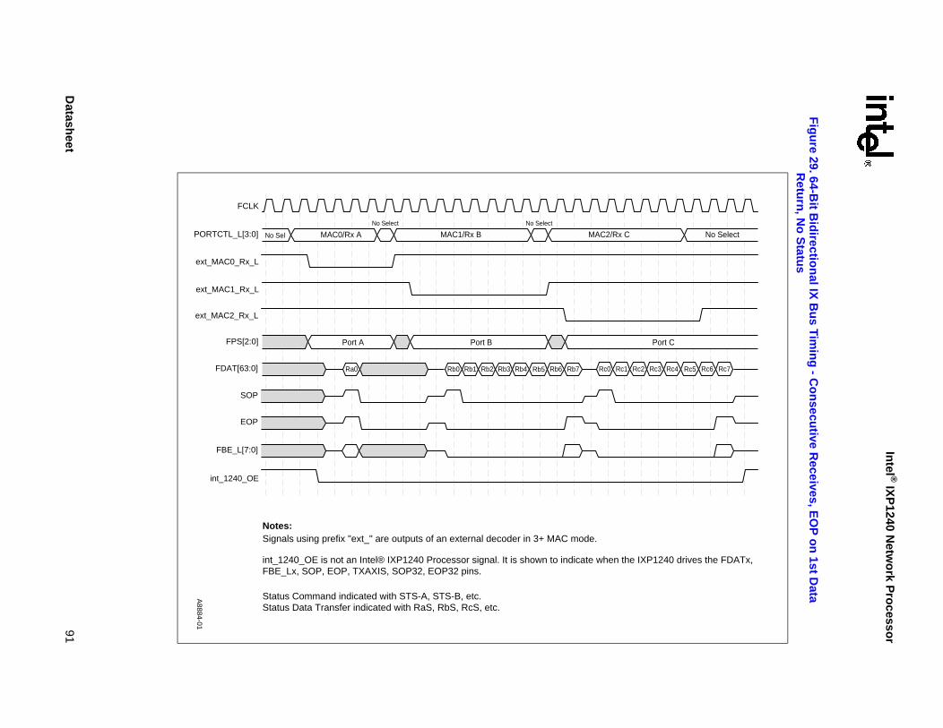
Intel ® IX
P1240 N
etwo
rk Pro
cessor
Datash
eet91
Fig
ure 29. 64-B
it Bid
irection
al IX B
us Tim
ing
- Co
nsecu
tive Receives, E
OP
on
1st Data
Retu
rn, N
o S
tatus
240 drives the FDATx,
No Select
ort C
3 Rc4 Rc5 Rc6 Rc7
A8884-01
FCLK
Notes:Signals using prefix "ext_" are outputs of an external decoder in 3+ MAC mode.
int_1240_OE is not an Intel® IXP1240 Processor signal. It is shown to indicate when the IXP1FBE_Lx, SOP, EOP, TXAXIS, SOP32, EOP32 pins.
Status Command indicated with STS-A, STS-B, etc.Status Data Transfer indicated with RaS, RbS, RcS, etc.
PORTCTL_L[3:0] MAC0/Rx A MAC1/Rx BNo Select No Select
No Sel MAC2/Rx C
ext_MAC0_Rx_L
ext_MAC1_Rx_L
ext_MAC2_Rx_L
FPS[2:0] Port A Port B P
FDAT[63:0] Ra0 Rb1Rb0 Rb2 Rb3 Rb4 Rb5 Rb6 Rb7 Rc1Rc0 Rc2 Rc
SOP
EOP
FBE_L[7:0]
int_1240_OE

Intel ® IX
P1240 N
etwo
rk Pro
cessor
92 D
atasheet
Fig
ure 30. 64-B
it Bid
irection
al IX B
us Tim
ing
- Co
nsecu
tive Receives, N
o E
OP
the IXP1240 drives the FDATx,
MAC2/Rx C
Port C
Rc1 Rc2 Rc3 Rc4 Rc5 RcRc0
A8885-01
FCLK
Notes:Signals using prefix "ext_" are outputs of an external decoder in 3+ MAC mode.
Status Command indicated with STS-A, STS-B, etc.Status Data Transfer indicated with RaS, RbS, RcS, etc.
int_1240_OE is not anIntel® IXP1240 Processor signal. It is shown to indicate whenFBE_Lx, SOP, EOP, TXAXIS, SOP32, EOP32 pins.
PORTCTL_L[3:0] MAC0/Rx A MAC1/Rx B
No Select No Select No Select
ext_MAC0_Rx_L
ext_MAC1_Rx_L
ext_MAC2_Rx_L
FPS[2:0] Port A Port B
FDAT[63:0] Ra0 Ra1 Ra2 Ra3 Ra4 Ra5 Ra6 Ra7 Rb0 Rb1 Rb2 Rb3 Rb4 Rb5 Rb6 Rb7
SOP
EOP
FBE_L[7:0]
int_1240_OE

Intel ® IX
P1240 N
etwo
rk Pro
cessor
Datash
eet93
Fig
ure 31. 64-B
it Bid
irection
al IX B
us T
imin
g - C
on
secutive R
eceives, EO
P o
n 8th
Data R
eturn
w
ith S
tatus
1240 drives the FDATx,
STS-BNoSel
NoSel
Port B
RbSRc4 Rc5 Rc6 Rc7
A8886-01
FCLK
Notes:Signals using prefix "ext_" are outputs of an external decoder in 3+ MAC mode.
int_1240_OE is not an Intel® IXP1240 Processor signal. It is shown to indicate when the IXPFBE_Lx, SOP, EOP, TXAXIS, SOP32, EOP32 pins.
Status Command indicated with STS-A, STS-B, etc.Status Data Transfer indicated with RaS, RbS, RcS, etc.
MAC0/Rx A MAC1/Rx BNoSel
STS-ANoSel
NoSel MAC2/Rx CPORTCTL_L[3:0]
ext_MAC0_Rx_L
ext_MAC1_Rx_L
ext_MAC2_Rx_L
Port A Port B
Port A
Port CFPS[2:0]
Ra0 Ra1 Ra2 Ra3FDAT[63:0] Rb0 RaSRb1 Rb2 Rb3 Rc0 Rc1 Rc2 Rc3Ra4 Ra5 Ra6 Ra7 Rb4 Rb5 Rb6 Rb7
SOP
EOP
FBE_L[7:0]
int_1240_OE

Intel ® IX
P1240 N
etwo
rk Pro
cessor
94 D
atasheet
Fig
ure 32. 64-B
it Bid
irection
al IX B
us Tim
ing
- Co
nsecu
tive Receives, E
OP
on
7th D
ata Retu
rn
with
Statu
s
P1240 drives the FDATx,
x C No Select
Port C
c1 Rc2 Rc3 Rc4 Rc5 Rc6 RcS
A8887-01
FCLK
Notes:Signals using prefix "ext_" are outputs of an external decoder in 3+ MAC mode.
Status Command indicated with STS-A, STS-B, etc.Status Data Transfer indicated with RaS, RbS, RcS, etc.
int_1240_OE is not an Intel® IXP1240 Processor signal. It is shown to indicate when the IXFBE_Lx, SOP, EOP, TXAXIS, SOP32, EOP32 pins.
PORTCTL_L[3:0] MAC0/Rx A MAC1/Rx B
No Select No Select
MAC2/R
ext_MAC0_Rx_L
ext_MAC1_Rx_L
ext_MAC2_Rx_L
FPS[2:0] Port A Port B
FDAT[63:0] Ra0 Ra1 Ra2 Ra3 Ra4 Ra5 Ra6 RaS Rb0 Rb1 Rb2 Rb3 Rb4 Rb5 Rb6 RbS RRc0
SOP
EOP
FBE_L[7:0]
int_1240_OE
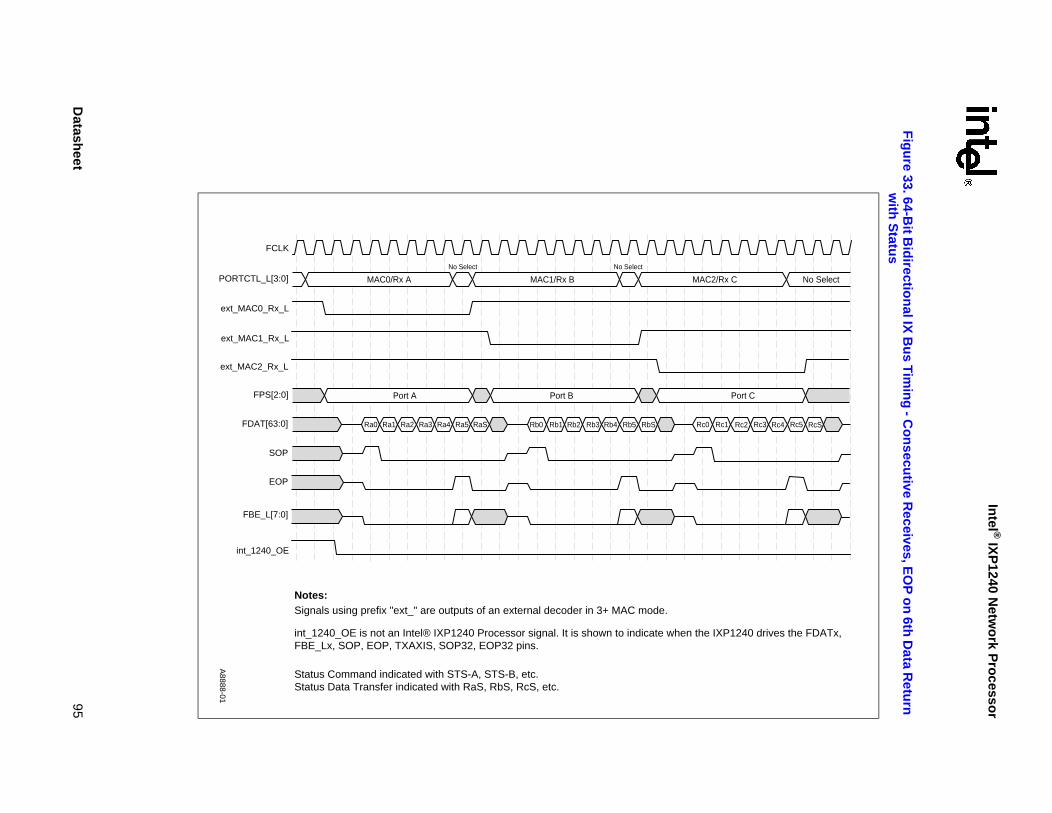
Intel ® IX
P1240 N
etwo
rk Pro
cessor
Datash
eet95
Fig
ure 33. 64-B
it Bid
irection
al IX B
us T
imin
g - C
on
secutive R
eceives, EO
P o
n 6th
Data R
eturn
w
ith S
tatus
240 drives the FDATx,
C No Select
Port C
Rc2 Rc3 Rc4 Rc5 RcS
A8888-01
FCLK
Notes:Signals using prefix "ext_" are outputs of an external decoder in 3+ MAC mode.
Status Command indicated with STS-A, STS-B, etc.Status Data Transfer indicated with RaS, RbS, RcS, etc.
int_1240_OE is not an Intel® IXP1240 Processor signal. It is shown to indicate when the IXP1FBE_Lx, SOP, EOP, TXAXIS, SOP32, EOP32 pins.
PORTCTL_L[3:0] MAC0/Rx A MAC1/Rx B
No Select No Select
MAC2/Rx
ext_MAC0_Rx_L
ext_MAC1_Rx_L
ext_MAC2_Rx_L
FPS[2:0] Port A Port B
FDAT[63:0] Ra0 Ra1 Ra2 Ra3 Ra4 Ra5 RaS Rb0 Rb1 Rb2 Rb3 Rb4 Rb5 RbS Rc1Rc0
SOP
EOP
FBE_L[7:0]
int_1240_OE
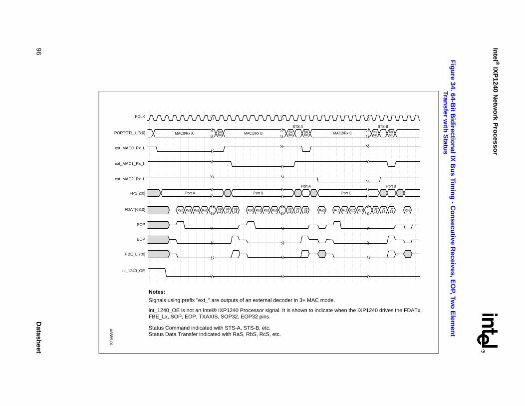
Intel ® IX
P1240 N
etwo
rk Pro
cessor
96 D
atasheet
Fig
ure 34. 64-B
it Bid
irection
al IX B
us Tim
ing
- Co
nsecu
tive Receives, E
OP, Tw
o E
lemen
t Tran
sfer with
Statu
s
P1240 drives the FDATx,
STS-BNoSel
NoSel
Port B
RbSc3 Rc13
Rc14
Rc15
A8889-01
FCLK
Notes:
Signals using prefix "ext_" are outputs of an external decoder in 3+ MAC mode.
int_1240_OE is not an Intel® IXP1240 Processor signal. It is shown to indicate when the IXFBE_Lx, SOP, EOP, TXAXIS, SOP32, EOP32 pins.
Status Command indicated with STS-A, STS-B, etc.Status Data Transfer indicated with RaS, RbS, RcS, etc.
MAC0/Rx A MAC1/Rx BNoSel
STS-ANoSel
NoSel MAC2/Rx CPORTCTL_L[3:0]
ext_MAC0_Rx_L
ext_MAC1_Rx_L
ext_MAC2_Rx_L
Port A Port B
Port A
Port CFPS[2:0]
Ra0 Ra1 Ra2 Ra3 Ra13
Ra14
Ra15FDAT[63:0] Rb0 RaSRb1 Rb2 Rb3 Rb
13Rb14
Rb15 Rc0 Rc1 Rc2 R
SOP
EOP
FBE_L[7:0]
int_1240_OE
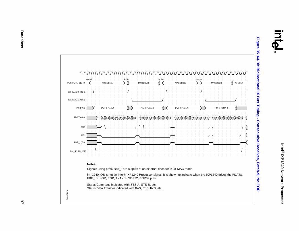
Intel ® IX
P1240 N
etwo
rk Pro
cessor
Datash
eet97
Fig
ure 35. 64-B
it Bid
irection
al IX B
us Tim
ing
- Co
nsecu
tive Receives, F
etch-9, N
o E
OP
P1240 drives the FDATx,
MAC1/Rx D No Select
Port D Fetch-8
Rd0 Rd1 Rd2 Rd38 Rd4 Rd5 Rd6 Rd7
A8890-01
FCLK
Notes:
Signals using prefix "ext_" are outputs of an external decoder in 3+ MAC mode.
int_1240_OE is not an Intel® IXP1240 Processor signal. It is shown to indicate when the IXFBE_Lx, SOP, EOP, TXAXIS, SOP32, EOP32 pins.
Status Command indicated with STS-A, STS-B, etc.Status Data Transfer indicated with RaS, RbS, RcS, etc.
MAC0/Rx A MAC1/Rx B MAC0/Rx C
No SelNo SelNo SelNo Sel
PORTCTL_L[7 :0]
ext_MAC0_Rx_L
ext_MAC1_Rx_L
Port A Fetch-9 Port B Fetch-8 Port C Fetch-9FPS[2:0]
Ra0 Ra1 Ra2 Ra3 Ra4 Ra5 Ra6 Ra7 Ra8 Rb0 Rb1 Rb2 Rb3 Rb4 Rb5 Rb6 Rb7FDAT[63:0] Rc0 Rc1 Rc2 Rc3 Rc4 Rc5 Rc6 Rc7 Rc
SOP
EOP
FBE_L[7:0]
int_1240_OE
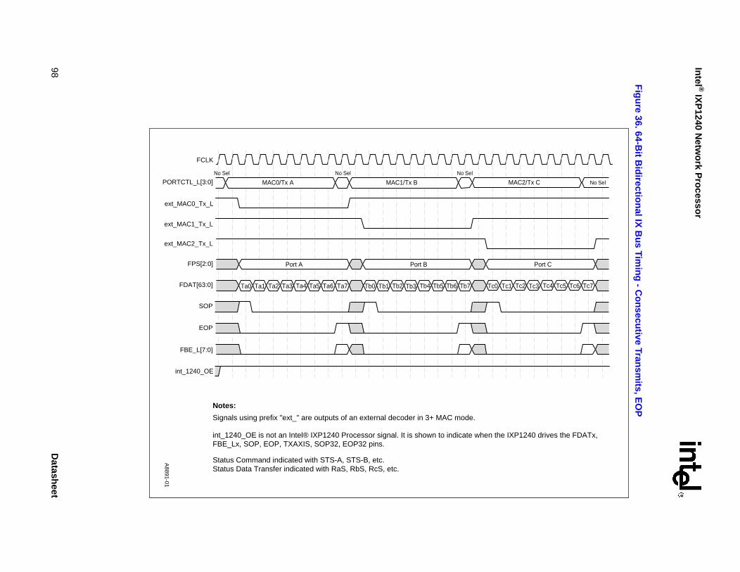
Intel ® IX
P1240 N
etwo
rk Pro
cessor
98 D
atasheet
Fig
ure 36. 64-B
it Bid
irection
al IX B
us Tim
ing
- Co
nsecu
tive Transm
its, EO
P
IXP1240 drives the FDATx,
MAC2/Tx C No Sel
Port C
1 Tc2 Tc4 Tc5 Tc6 Tc7Tc3
A8891-01
FCLK
Notes:
Signals using prefix "ext_" are outputs of an external decoder in 3+ MAC mode.
int_1240_OE is not an Intel® IXP1240 Processor signal. It is shown to indicate when the FBE_Lx, SOP, EOP, TXAXIS, SOP32, EOP32 pins.
Status Command indicated with STS-A, STS-B, etc.Status Data Transfer indicated with RaS, RbS, RcS, etc.
PORTCTL_L[3:0] MAC0/Tx A
No Sel
MAC1/Tx B
No SelNo Sel
ext_MAC0_Tx_L
ext_MAC1_Tx_L
ext_MAC2_Tx_L
FPS[2:0] Port A Port B
FDAT[63:0] Ta0 Ta1 Ta2 Ta4 Ta5 Ta6 Ta7Ta3 Tb0 Tb1 Tb2 Tb4 Tb5 Tb6 Tb7Tb3 Tc0 Tc
SOP
EOP
FBE_L[7:0]
int_1240_OE
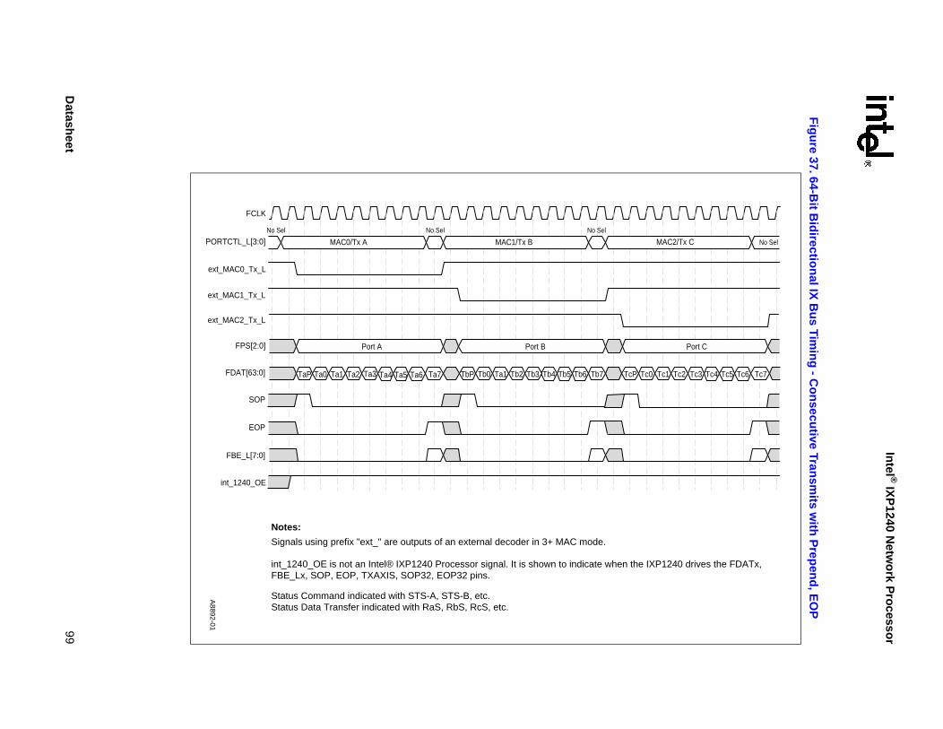
Intel ® IX
P1240 N
etwo
rk Pro
cessor
Datash
eet99
Fig
ure 37. 64-B
it Bid
irection
al IX B
us Tim
ing
- Co
nsecu
tive Transm
its with
Prep
end
, EO
P
P1240 drives the FDATx,
MAC2/Tx C No Sel
Port C
Tc7Tc1 Tc2 Tc6Tc5Tc4Tc3
A8892-01
FCLK
Notes:
Signals using prefix "ext_" are outputs of an external decoder in 3+ MAC mode.
int_1240_OE is not an Intel® IXP1240 Processor signal. It is shown to indicate when the IXFBE_Lx, SOP, EOP, TXAXIS, SOP32, EOP32 pins.
Status Command indicated with STS-A, STS-B, etc.Status Data Transfer indicated with RaS, RbS, RcS, etc.
PORTCTL_L[3:0] MAC0/Tx A
No Sel
MAC1/Tx B
No SelNo Sel
ext_MAC0_Tx_L
ext_MAC1_Tx_L
ext_MAC2_Tx_L
FPS[2:0] Port A Port B
FDAT[63:0] Ta7TaP Ta0 Ta1 Ta2 Ta6Ta5Ta4Ta3 Tb7TbP Tb0 Ta1 Tb2 Tb6Tb5Tb4Tb3 TcP Tc0
SOP
EOP
FBE_L[7:0]
int_1240_OE

Intel ® IX
P1240 N
etwo
rk Pro
cessor
100 D
atasheet
Fig
ure 38. 32-B
it Un
idirectio
nal IX
Bu
s Timin
g - C
on
secutive R
eceives, No
EO
P
IXP1240 drives the
MAC2/Rx D No Select
Port D
Rd0 Rd1 Rd2 Rd3 Rd13
Rd14
Rd15
A8893-01
FCLK
Notes:
Signals using prefix "ext_" are outputs of an external decoder in 3+ MAC mode.
int_1240_OE is not an Intel® IXP1240 Processor signal. It is shown to indicate when theFDATx, FBE_Lx, SOP, EOP, TXAXIS, SOP32, EOP32 pins.
MAC0/Rx A MAC1/Rx B MAC2/Rx B
No SelNo SelNo Sel
PORTCTL_L[1 :0]
RDYCTL_L[4]( used with PORTCTL_L 3+ MAC mode only )
ext_MAC0_Rx_L
ext_MAC1_Rx_L
ext_MAC2_Rx_L
ext_MAC3_Rx_L
Port A Port B Port CFPS[2:0]
Ra0 Ra1 Ra2 Ra3 Ra13
Ra14
Ra15 Rb0 Rb1 Rb2 Rb3 Rb
13Rb14
Rb15FDAT[31:0] Rc0 Rc1 Rc2 Rc3 Rc
13Rc14
Rc15
SOP
EOP
FBE_L[3:0]

Intel ® IX
P1240 N
etwo
rk Pro
cessor
Datash
eet101
Fig
ure 39. 32-B
it Un
idirectio
nal IX
Bu
s Timin
g - C
on
secutive R
eceives, EO
P o
n 16th
Data
Retu
rn w
ith S
tatus
/Rx D No Select
No Sel
STS-C
Port D
Port C
Rd13
Rd14
Rd15Rd0 Rd1
A8561-01
FCLK
Notes:Signals using prefix "ext_" are outputs of an external decoder in 3+ MAC mode.
Status Command indicated with STS-A, STS-B, etc.Status Data Transfer indicated with RaS, RbS, RcS, etc.
MAC0/Rx A MAC1/Rx B MAC2/Rx C MAC3
No SelNo Sel No Sel
STS-A
No SelNo Sel
PORTCTL_L[1:0]
No Sel
STS-B( used with PORTCTL_L 3+ MAC mode only )RDYCTL_L[4]
ext_MAC0_Rx_L
ext_MAC1_Rx_L
ext_MAC2_Rx_L
ext_MAC3_Rx_L
Port A Port B Port CFPS[2:0]
Port A Port B
Ra0 Ra1 Ra14
Ra13
Ra15 Rb0 Rb1 Rb
14Rb15
Rb13FDAT[31:0] Rc1Rc0 Rc
13Rc14
Rc15 RbSRaS
SOP
EOP
FBE_L[3:0]

Intel ® IX
P1240 N
etwo
rk Pro
cessor
102 D
atasheet
Fig
ure 40. 32-B
it Un
idirectio
nal IX
Bu
s Timin
g - C
on
secutive R
eceives, EO
P o
n 15th
Data
Retu
rn w
ith S
tatus
P1240 drives the FDATx,
3/Rx D No Select
ort D
0 Rd1 Rd2 Rd3 Rd13
Rd14 RdS
A8894-01
FCLK
Notes:Signals using prefix "ext_" are outputs of an external decoder in 3+ MAC mode.
int_1240_OE is not an Intel® IXP1240 Processor signal. It is shown to indicate when the IXFBE_Lx, SOP, EOP, TXAXIS, SOP32, EOP32 pins.
MAC0/Rx A MAC1/Rx B MAC2/Rx C MAC
No SelNo SelNo SelNo Sel
PORTCTL_L[1:0]
RDYCTL_L[4]( used with PORTCTL_L 3+ MAC mode only )
ext_MAC0_Rx_L
ext_MAC1_Rx_L
ext_MAC2_Rx_L
ext_MAC3_Rx_L
Port A Port B Port C PFPS[2:0]
Ra0 Ra1 Ra2 Ra3 Ra13
Ra14 Rb0 Rb1 Rb2 Rb3 Rb
13Rb14FDAT[31:0] Rc0 Rc1 Rc2 Rc3 Rc
13Rc14 RdRaS RbS RcS
SOP
EOP
FBE_L[3:0]

Intel ® IX
P1240 N
etwo
rk Pro
cessor
Datash
eet103
Fig
ure 41. 32-B
it Un
idirectio
nal IX
Bu
s Timin
g - C
on
secutive R
eceives, EO
P o
n 14th
Data
Retu
rn w
ith S
tatus
1240 drives the
x D No Select
ort D
d1 Rd2 Rd3 Rd13 RdS
A8895-01
FCLK
Notes:
Signals using prefix "ext_" are outputs of an external decoder in 3+ MAC mode.
int_1240_OE is not an Intel® IXP1240 Processor signal. It is shown to indicate when the IXPFDATx, FBE_Lx, SOP, EOP, TXAXIS, SOP32, EOP32 pins. .
MAC0/Rx A MAC1/Rx B MAC2/Rx C MAC3/R
No SelNo SelNo SelNo Sel
PORTCTL_L[1:0]
RDYCTL_L[4]( used with PORTCTL_L 3+ MAC mode only )
ext_MAC0_Rx_L
ext_MAC1_Rx_L
ext_MAC2_Rx_L
ext_MAC3_Rx_L
Port A Port B Port C PFPS[2:0]
Ra0 Ra1 Ra2 Ra3 Ra13 Rb0 Rb1 Rb2 Rb3 Rb
13FDAT[31:0] Rc0 Rc1 Rc2 Rc3 Rc13 Rd0 RRaS RbS RcS
SOP
EOP
FBE_L[3:0]

Intel ® IX
P1240 N
etwo
rk Pro
cessor
104 D
atasheet
Fig
ure 42. 32-B
it Un
idirectio
nal IX
Bu
s Timin
g - C
on
secutive R
eceives, EO
P o
n 1st T
hro
ug
h
13th D
ata Retu
rn w
ith S
tatus (13th
Data R
eturn
Sh
ow
n)
3/Rx C No Select
Port D
0 Rd1 Rd2 Rd12 RdS
A8563-01
FCLK
Notes:Signals using prefix "ext_" are outputs of an external decoder in 3+ MAC mode.
Status Command indicated with STS-A, STS-B, etc.Status Data Transfer indicated with RaS, RbS, RcS, etc.
MAC0/Rx A MAC1/Rx B MAC2/Rx C MAC
No SelNo SelNo SelNo Sel
PORTCTL_L[1:0]
( used with PORTCTL_L 3+ MAC mode only )RDYCTL_L[4]
ext_MAC0_Rx_L
ext_MAC1_Rx_L
ext_MAC2_Rx_L
ext_MAC3_Rx_L
Port A Port B Port CFPS[2:0]
Ra0 Ra1 Ra2 Ra12 Rb0 Rb1 Rb2 Rb
12FDAT[31:0] Rc0 Rc1 Rc2 Rc12 RdRaS RbS RcS
SOP
EOP
FBE_L[3:0]

Intel ® IX
P1240 N
etwo
rk Pro
cessor
Datash
eet105
Fig
ure 43. 32-B
it Un
idirectio
nal IX
Bu
s Timin
g - C
on
secutive R
eceives, EO
P, 64-Bit S
tatus
MAC0/Rx DNoSel
NoSel
ort B Port D
Rd0 Rd1 Rdc5
RaS1e
RbS0
A8592-01
FCLK
Notes:Signals using prefix "ext_" are outputs of an external decoder in 3+ MAC mode.Status Command indicated with STS-A, STS-B, etc.Status Data Transfer indicated with RaS0, RaS1e, RbS0, RbS1e etc.
MAC0/Rx A MAC0/Rx BNoSel STS-ANo
SelNoSel MAC0/Rx C STS-BNo
SelPORTCTL_L[1:0]
RDYCTL_L[4]( used with PORTCTL_L 3+ MAC mode only )
ext_MAC0_Rx_L
ext_MAC1_Rx_L
ext_MAC2_Rx_L
ext_MAC3_Rx_L
Port A Port B Port A Port C PFPS[2:0]
Ra0 Ra1 Rb0 Rb1 RaS0 Rc0 Rc1Ra
13Ra14
Ra15
FDAT[31:0] Rb14
Rb15
Rc13
Rc14
R1
RaS1e
Rb13
SOP
EOP
FBE_L[3:0]
Intel ® IX
P1240 N
etwo
rk Pro
cessor
106 D
atasheet
Fig
ure 44. 32-B
it Un
idirectio
nal IX
Bu
s Timin
g - C
on
secutive R
eceives, Two
Elem
ent
Transfers w
ith 32-B
it Statu
s
C3/Rx D
STS-CNoSel No Sel
Port C
Port D
Rd0 Rd1 Rd29
Rd30
Rd31
A8593-01
FCLK
Notes:Signals using prefix "ext_" are outputs of an external decoder in 3+ MAC mode.
Status Command indicated with STS-A, STS-B, etc.Status Data Transfer indicated with RaS0, RaS1e, RbS0, RbS1e etc.
MAC0/Rx A MAC1/Rx BNoSel
NoSel
STS-ANoSel
NoSel MAC2/Rx C MA
STS-BNoSel
NoSelPORTCTL_L[1:0]
RDYCTL_L[4]( used with PORTCTL_L 3+ MAC mode only )
ext_MAC0_Rx_L
ext_MAC1_Rx_L
ext_MAC2_Rx_L
ext_MAC3_Rx_L
Port A Port B
Port A
Port C
Port B
FPS[2:0]
Ra0 Ra1 Rb0 Rb1 Rc0 Rc1Ra29
Ra30
Ra31FDAT[31:0] Rb
30Rb31
Rc29
Rc30
Rc31
Rb29 RaS RbS
SOP
EOP
FBE_L[3:0]
Intel ® IX
P1240 N
etwo
rk Pro
cessor
Datash
eet107
Fig
ure 45. 32-B
it Un
idirectio
nal IX
Bu
s Timin
g - C
on
secutive Tran
smits, E
OP
MAC2/Tx C No Select
Port C
Tc1 Tc2 Tc3 Tc15
A8594-01
FCLK
Notes:Signals using prefix "ext_" are outputs of an external decoder in 3+ MAC mode.
Status Command indicated with STS-A, STS-B, etc.Status Data Transfer indicated with RaS, RbS, RcS, etc.
MAC0/Tx A
No Sel
MAC1/Tx B
No SelNo Sel
PORTCTL_L[3:2]
( used with PORTCTL_L 3+ MAC mode only )
GPIO[0]
ext_MAC0_Tx_L
ext_MAC1_Tx_L
ext_MAC2_Tx_L
Port A Port BGPIO[3:1]
Ta0 Ta1 Ta2 Ta3 Ta15 Tb0 Tb1 Tb2 Tb15 Tc0FDAT[31:0] Tb3
SOP32
EOP32
FBE_L[7:4]

Intel ® IX
P1240 N
etwo
rk Pro
cessor
108 D
atasheet
Fig
ure 46. 32-B
it Un
idirectio
nal IX
Bu
s Timin
g - C
on
secutive Tran
smits w
ith P
repen
d, E
OP
MAC2/Tx C No Select
Port C
Tc0 Tc1 Tc2 Tc15cP1 Tc14
A8595-01
FCLK
Notes:Signals using prefix "ext_" are outputs of an external decoder in 3+ MAC mode.
Status Command indicated with STS-A, STS-B, etc.Status Data Transfer indicated with RaS, RbS, RcS, etc.
MAC0/Tx A MAC1/Tx B
No SelNo Sel
PORTCTL_L[3:2]
( used with PORTCTL_L 3+ MAC mode only )
GPIO[0]
ext_MAC0_Tx_L
ext_MAC1_Tx_L
ext_MAC2_Tx_L
Port A Port BGPIO[3:1]
TaP0 Ta0 Ta1 Ta2 Ta14 Ta15FDAT[31:0] TaP
1TbP
0 Tb0 Tb1 Tb2 Tb15TbP1 Tb14 TcP
0T
SOP32
EOP32
FBE_L[7:4]
Intel ® IX
P1240 N
etwo
rk Pro
cessor
Datash
eet109
Fig
ure 47. 64-B
it Bid
irection
al IX B
us Tim
ing
- Co
nsecu
tive FastP
ort R
eceives, Sam
e Po
rt, E
OP, N
o S
tatus, F
P_R
EA
DY
_WA
IT=0
Number of NoSelect Cycles____________23456
elect cycles depends sampled:
No Select
Rf5 Rf6 Rf7
A8896-01
FCLK
Data Cycle EOPis sampled____________Rf0-Rf3Rf4Rf5Rf6Rf7
Notes:
Signals using prefix "ext_" are outputs of an external decoder in 3+ MAC mode. * Number of No Son when EOP is
int_1240_OE is not an Intel® IXP1240 Processor signal. It is shown to indicate whenthe IXP1240 drives the FDATx, FBE_Lx, SOP, EOP, TXAXIS, SOP32, EOP32 pins.
Status Command indicated with STS-A, STS-B, etc.Status Data Transfer indicated with RaS, RbS, RcS, etc.
PORTCTL_L[3:0] FastPort/Rx Port 0 req_L1 FastPort/Rx Port 0 req_L2No Select - See Footnote*NoSel
ext_MAC0_Rx_L
FPS[2:0] Port 0 Port 0
FDAT[63:0] Rf0 Rf1 Rf2 Rf4 Rf5 Rf6 Rf7Rf3 Rf0 Rf1 Rf2 Rf4Rf3
SOP
EOP
FAST_RX1
FAST_RX sampledregister FP_READY_WAIT=0
int_1240_OE
FBE_L[7:0]
Intel ® IX
P1240 N
etwo
rk Pro
cessor
110 D
atasheet
Fig
ure 48. 64-B
it Bid
irection
al IX B
us Tim
ing
- Co
nsecu
tive FastP
ort R
eceives, Sam
e Po
rt, E
OP, N
o S
tatus, F
P_R
EA
DY
_WA
IT=5
Number of NoSelect Cycles____________2 + FP_READY_WAIT value3 + FP_READY_WAIT value4 + FP_READY_WAIT value5 + FP_READY_WAIT value6 + FP_READY_WAIT value
elect cycles depends sampled:
eq_L2 No Select
0
2 Rf4 Rf5 Rf6 Rf7Rf3
A8897-01
FCLK
Data Cycle EOPis sampled____________Rf0-Rf3Rf4Rf5Rf6Rf7
Notes:
Signals using prefix "ext_" are outputs of an external decoder in 3+ MAC mode.
int_1240_OE is not an Intel® IXP1240 Processor signal. It is shown to indicate whenthe IXP1240 drives the FDATx, FBE_Lx, SOP, EOP, TXAXIS, SOP32, EOP32 pins.
Status Command indicated with STS-A, STS-B, etc.Status Data Transfer indicated with RaS, RbS, RcS, etc.
* Number of No Son when EOP is
PORTCTL_L[3:0] FastPort/Rx Port 0 req_L1 FastPort/Rx Port 0 rNo Select - See Footnote*NoSel
ext_MAC0_Rx_L
FPS[2:0] Port 0 Port
FDAT[63:0] Rf0 Rf1 Rf2 Rf4 Rf5 Rf6 Rf7Rf3 Rf0 Rf1 Rf
SOP
EOP
FBE_L[7:0]
FAST_RX1
FAST_RX sampledregister FP_READY_WAIT=5
int_1240_OE
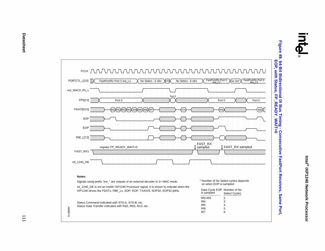
Intel ® IX
P1240 N
etwo
rk Pro
cessor
Datash
eet111
Fig
ure 49. 64-B
it Bid
irection
al IX B
us Tim
ing
- Co
nsecu
tive FastP
ort R
eceives, Sam
e Po
rt, E
OP, w
ith S
tatus, F
P_R
EA
DY
_WA
IT=0
umber of Noelect Cycles_________
ct cycles dependsmpled:
FastPort/Rx Port 0req_L3No Sel*
Port 0
Rf0
AST_RX sampled
A8898-01
FCLK
Data Cycle EOPis sampled____________Rf0-Rf3Rf4Rf5Rf6Rf7
NS__2 3 4 5 6
Notes:
Signals using prefix "ext_" are outputs of an external decoder in 3+ MAC mode.
int_1240_OE is not an Intel® IXP1240 Processor signal. It is shown to indicate when theIXP1240 drives the FDATx, FBE_Lx, SOP, EOP, TXAXIS, SOP32, EOP32 pins.
Status Command indicated with STS-A, STS-B, etc.Status Data Transfer indicated with RaS, RbS, RcS, etc.
* Number of No Seleon when EOP is sa
PORTCTL_L[3:0] FastPort/Rx Port 0 req_L1 FastPort/Rx Port 0req_L2No Select - 5 clks No Select - 6 clksSTSNo
Sel
ext_MAC0_Rx_L
FPS[2:0] Port 0 Port 0Port 0
FDAT[63:0] Rf0 Rf1 Rf2 Rf4 Rf5 Rf6 Rf7 STSRf3 Rf0
SOP
EOP
FBE_L[7:0]
FAST_RX1
FAST_RXsampledregister FP_READY_WAIT=0 F
int_1240_OE

Intel ® IX
P1240 N
etwo
rk Pro
cessor
112 D
atasheet
Fig
ure 50. 64-B
it Bid
irection
al IX B
us Tim
ing
- Co
nsecu
tive FastP
ort R
eceives, Sam
e Po
rt, E
OP, N
o S
tatus, F
P_R
EA
DY
_WA
IT=5
FDATx,
No SelectNo Select 5 clks STS
Port 0
4 Rf5 Rf6 Rf7 RfS
A8899-01
FCLK
Notes:
Signals using prefix "ext_" are outputs of an external decoder in 3+ MAC mode.
int_1240_OE is not an Intel® IXP1240 Processor signal. It is shown to indicate when the IXP1240 drives theFBE_Lx,SOP, EOP, TXAXIS, SOP32, EOP32 pins.
Status Command indicated with STS-A, STS-B, etc.Status Data Transfer indicated with RaS, RbS, RcS, etc.
PORTCTL_L[3:0] FastPort/Rx Port 0 req_L1 FastPort/Rx Port 0 req_L2No Select-5 clks No Select-11 clksSTS
ext_MAC0_Rx_L
FPS[2:0] Port 0 Port 0Port 0
FDAT[63:0] Rf0 Rf1 Rf2 Rf3 Rf4 Rf5 Rf6 Rf7 Rf0 Rf1 Rf2 Rf3 RfRfS
SOP
EOP
FBE_L[7:0]
FAST_RX1
FAST_RX sampledregister FP_READY_WAIT=5
int_1240_OE
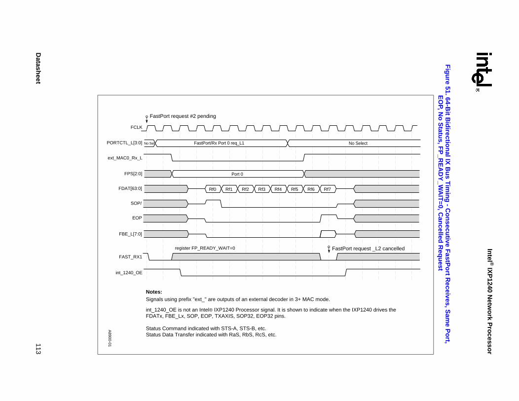
Intel ® IX
P1240 N
etwo
rk Pro
cessor
Datash
eet113
Fig
ure 51. 64-B
it Bid
irection
al IX B
us Tim
ing
- Co
nsecu
tive FastP
ort R
eceives, Sam
e Po
rt, E
OP, N
o S
tatus, F
P_R
EA
DY
_WA
IT=0, C
ancelled
Req
uest
1240 drives the
lect
uest _L2 cancelled
A8900-01
FCLK
FastPort request #2 pending
Notes:Signals using prefix "ext_" are outputs of an external decoder in 3+ MAC mode.
int_1240_OE is not an Intel® IXP1240 Processor signal. It is shown to indicate when the IXPFDATx, FBE_Lx, SOP, EOP, TXAXIS, SOP32, EOP32 pins.
Status Command indicated with STS-A, STS-B, etc.Status Data Transfer indicated with RaS, RbS, RcS, etc.
PORTCTL_L[3:0] FastPort/Rx Port 0 req_L1 No SeNo Sel
ext_MAC0_Rx_L
FPS[2:0] Port 0
FDAT[63:0] Rf0 Rf1 Rf2 Rf3 Rf4 Rf5 Rf6 Rf7
SOP/
EOP
FBE_L[7:0]
FAST_RX1
FastPort reqregister FP_READY_WAIT=0
int_1240_OE
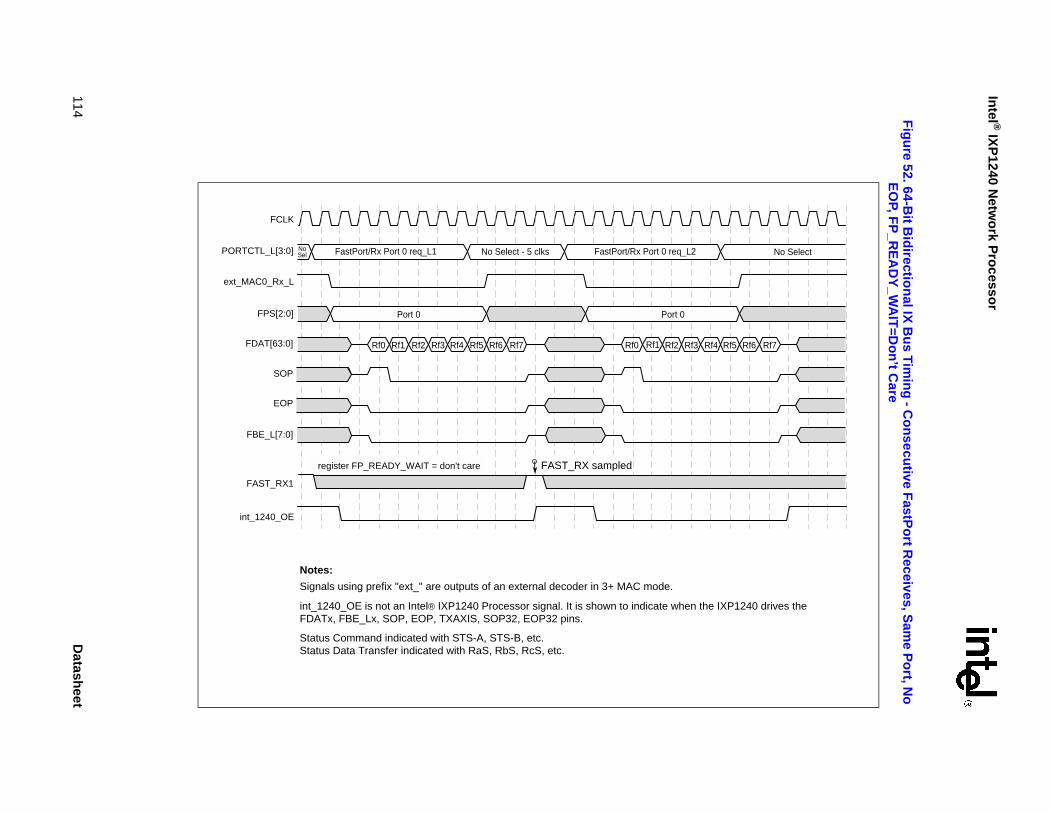
Intel ® IX
P1240 N
etwo
rk Pro
cessor
114 D
atasheet
Fig
ure 52. 64-B
it Bid
irection
al IX B
us T
imin
g - C
on
secutive F
astPo
rt Receives, S
ame P
ort, N
o
EO
P, FP
_RE
AD
Y_W
AIT
=Do
n’t C
are
XP1240 drives the
No Select
Rf5 Rf6 Rf7
FCLK
Notes:
Signals using prefix "ext_" are outputs of an external decoder in 3+ MAC mode.
int_1240_OE is not an Intel® IXP1240 Processor signal. It is shown to indicate when the IFDATx, FBE_Lx, SOP, EOP, TXAXIS, SOP32, EOP32 pins.
Status Command indicated with STS-A, STS-B, etc.Status Data Transfer indicated with RaS, RbS, RcS, etc.
PORTCTL_L[3:0] FastPort/Rx Port 0 req_L1 FastPort/Rx Port 0 req_L2No Select - 5 clksNoSel
ext_MAC0_Rx_L
FPS[2:0] Port 0 Port 0
FDAT[63:0] Rf0 Rf1 Rf2 Rf4 Rf5 Rf6 Rf7Rf3 Rf0 Rf1 Rf2 Rf4Rf3
SOP
EOP
FBE_L[7:0]
FAST_RX1
FAST_RX sampledregister FP_READY_WAIT = don't care
int_1240_OE

Intel ® IX
P1240 N
etwo
rk Pro
cessor
Datash
eet115
Fig
ure 53. 64-B
it Bid
irection
al IX B
us Tim
ing
- Co
nsecu
tive FastP
ort R
eceives, Differen
t P
orts, E
OP, N
o S
tatus, F
P_R
EA
DY
_WA
IT=0
40 drives the FDATx,
No Selectt/Rx Port 1 req_L2
Port 1
Rf0 Rf1 Rf2 Rf4 Rf5 Rf6 Rf7Rf3
or Port 1 req_L2 sampled
A8902-01
FCLK
Notes:Signals using prefix "ext_" are outputs of an external decoder in 3+ MAC mode.
Status Command indicated with STS-A, STS-B, etc.Status Data Transfer indicated with RaS, RbS, RcS, etc.
int_1240_OE is not an Intel® IXP1240 Processor signal. It is shown to indicate when the IXP12FBE_Lx, SOP, EOP, TXAXIS, SOP32, EOP32 pins.
PORTCTL_L[3:0] FastPort/Rx Port 0 req_L1 FastPort/Rx Port 1 req_L1 FastPort/Rx Port 0 req_L2No Sel No Sel
FastPorNo Sel
ext_MAC0_Rx_L
FPS[2:0] Port 0 Port 1 Port 0
FDAT[63:0] Rf0 Rf1 Rf2 Rf4 Rf5 Rf6 Rf7Rf3 Rf0 Rf1 Rf2 Rf4 Rf5 Rf6 Rf7Rf3 Rf0 Rf1 Rf2 Rf4 Rf5 Rf6 Rf7Rf3
SOP
EOP
FBE_L[7:0]
FAST_RX1
FAST_RX for Port 0 req_L2 sampledregister FP_READY_WAIT=0
FAST_RX2
FAST_RX for Port 1 req_L1 sampled FAST_RX f
int_1240_OE

Intel ® IX
P1240 N
etwo
rk Pro
cessor
116 D
atasheet
Fig
ure 54. 64-B
it Bid
irection
al IX B
us Tim
ing
- Co
nsecu
tive FastP
ort R
eceives, Differen
t P
orts, E
OP, N
o S
tatus, F
P_R
EA
DY
_WA
IT=0, C
ancelled
Req
uest
1240 drives the FDATx,
No Select/Rx Port 1 req_L2
Port 1
Rf0 Rf1 Rf2 Rf4 Rf5 Rf6 Rf7Rf3
r Port 1 req_L2 sampled
A8903-01
FCLK
Notes:Signals using prefix "ext_" are outputs of an external decoder in 3+ MAC mode.
Status Command indicated with STS-A, STS-B, etc.Status Data Transfer indicated with RaS, RbS, RcS, etc.
int_1240_OE is not an Intel® IXP1240 Processor signal. It is shown to indicate when the IXPFBE_Lx, SOP, EOP, TXAXIS, SOP32, EOP32 pins.
PORTCTL_L[3:0] FastPort/Rx Port 0 req_L1 No Select FastPort/Rx Port 0 req_L2 FastPortNo Sel
ext_MAC0_Rx_L
FPS[2:0] Port 0 Port 0
FDAT[63:0] Rf0 Rf1 Rf2 Rf4 Rf5 Rf6 Rf7Rf3 Rf0 Rf1 Rf2 Rf4 Rf5 Rf6 Rf7Rf3
SOP
EOP
FBE_L[7:0]
FAST_RX1
FAST_RX for Port 0 req_L2 sampledregister FP_READY_WAIT=0
FAST_RX2
FAST_RX for Port 1 req_L1 sampled- pending request cancelled
FAST_RX fo
int_1240_OE
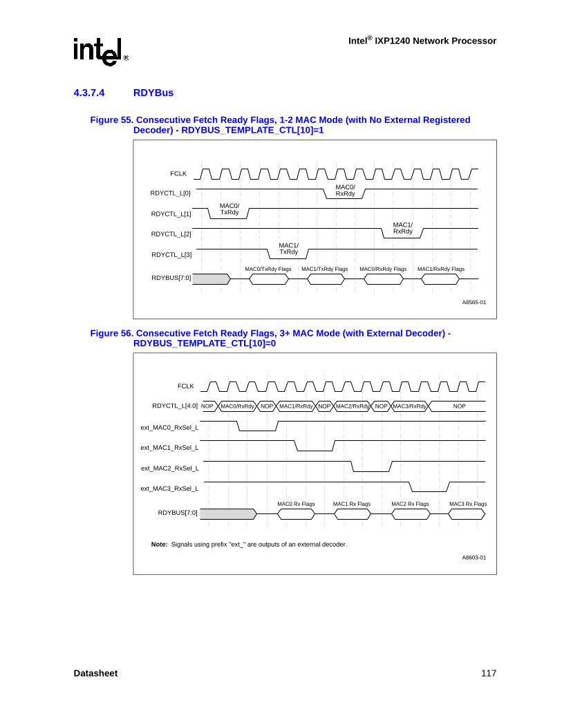
Intel® IXP1240 Network Processor
4.3.7.4 RDYBus
Figure 55. Consecutive Fetch Ready Flags, 1-2 MAC Mode (with No External Registered Decoder) - RDYBUS_TEMPLATE_CTL[10]=1
Figure 56. Consecutive Fetch Ready Flags, 3+ MAC Mode (with External Decoder) - RDYBUS_TEMPLATE_CTL[10]=0
A8565-01
RDYBUS[7:0]MAC0/TxRdy Flags MAC1/TxRdy Flags MAC0/RxRdy Flags MAC1/RxRdy Flags
RDYCTL_L[3]
MAC1/TxRdy
RDYCTL_L[2]MAC1/RxRdy
RDYCTL_L[1]MAC0/TxRdy
RDYCTL_L[0]MAC0/RxRdy
FCLK
A8603-01
Note: Signals using prefix "ext_" are outputs of an external decoder.
RDYBUS[7:0]MAC0 Rx Flags MAC1 Rx Flags MAC2 Rx Flags MAC3 Rx Flags
ext_MAC3_RxSel_L
ext_MAC2_RxSel_L
ext_MAC1_RxSel_L
ext_MAC0_RxSel_L
RDYCTL_L[4:0] NOP NOP NOPMAC0/RxRdy NOPMAC1/RxRdy MAC2/RxRdy NOPMAC3/RxRdy
FCLK
Datasheet 117
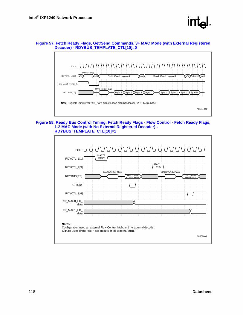
Intel® IXP1240 Network Processor
Figure 57. Fetch Ready Flags, Get/Send Commands, 3+ MAC Mode (with External Registered Decoder) - RDYBUS_TEMPLATE_CTL[10]=0
Figure 58. Ready Bus Control Timing, Fetch Ready Flags - Flow Control - Fetch Ready Flags, 1-2 MAC Mode (with No External Registered Decoder) - RDYBUS_TEMPLATE_CTL[10]=1
A8604-01
Note: Signals using prefix "ext_" are outputs of an external decoder in 3+ MAC mode.
RDYBUS[7:0]
MAC TxRdy Flags
Byte 3 Byte 2 Byte 1 Byte 0 Byte 3 Byte 2 Byte 1 Byte 0
ext_MAC0_TxRdy_L
RDYCTL_L[3:0]
MAC0/TxRdy
NOP NOP Get1, One Longword NOP NOP NOPAutopushSend, One Longword
FCLK
A8605-01
Notes:Configuration used an external Flow Control latch, and no external decoder.Signals using prefix "ext_" are outputs of the external latch.
ext_MAC1_FC_data
ext_MAC0_FC_data
RDYCTL_L[4]
GPIO[0]
MAC0/TxRdy Flags MAC1/TxRdy Flags
RDYBUS[7:0] MAC1 FlowControl Mask
MAC0 FlowControl Mask
RDYCTL_L[3]MAC1/TxRdy
RDYCTL_L[1]MAC0/TxRdy
FCLK
118 Datasheet
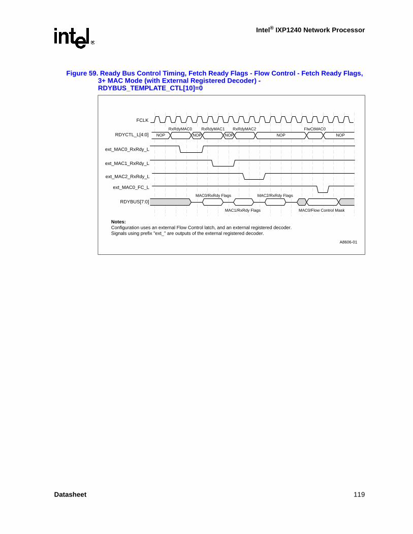
Intel® IXP1240 Network Processor
Figure 59. Ready Bus Control Timing, Fetch Ready Flags - Flow Control - Fetch Ready Flags, 3+ MAC Mode (with External Registered Decoder) - RDYBUS_TEMPLATE_CTL[10]=0
A8606-01
Notes:Configuration uses an external Flow Control latch, and an external registered decoder.Signals using prefix "ext_" are outputs of the external registered decoder.
RDYBUS[7:0]MAC0/RxRdy Flags MAC2/RxRdy Flags
MAC1/RxRdy Flags MAC0/Flow Control Mask
ext_MAC0_FC_L
ext_MAC2_RxRdy_L
ext_MAC1_RxRdy_L
ext_MAC0_RxRdy_L
RDYCTL_L[4:0] NOP NOP
RxRdyMAC0 RxRdyMAC1
NOP NOP
RxRdyMAC2
NOP
FlwCtMAC0
FCLK
Datasheet 119

Intel® IXP1240 Network Processor
4.3.7.5 TK_IN/TK_OUT
The following timing diagrams show the transition from one IX Bus owner to another. Note that prior to giving up the bus, the PORTCTL[4:0] signals are driven high which will not select any ports. Then the signal is tri-stated and must be held up with pullup resistors.
4.3.8 SRAM Interface
4.3.8.1 SRAM SCLK Signal AC Parameter Measurements
Vt1 = 0.5*VDDXVt2 = 0.4*VDDXVt3 = 0.3*VDDX
Figure 60. IX Bus Ownership Passing
Figure 61. SRAM SCLK Signal AC Parameter Measurements
A8904-01
1 2 3 4 5 6 7 8 9
FCLK
TK_OUT _L1(is TK_IN to _L2 )
FDAT[63:0]
A = Driven by the Intel® IXP1240 Network Processor _L1 if the transfer is a Tx, not drivenif the transfer is a Rx.
B = Driven high for one cycle by the IXP1200 Network Processor _L2 (no port is selected),then tristated.
C = Weak external pull-up resistors are recommended on PORTCTL_L[7:0], FPS[2:0] and TXAXIS.
PORTCTL_L[7:0]FPS[2:0]TXAXIS
Notes:
B C
TK_OUT _L2
Device 1 Releases Token Device 2 Now Has Token
Data A
A8608-01
Tcyc
TfTr
Vt3
Vt1
Vt2
Thigh
Tlow
120 Datasheet
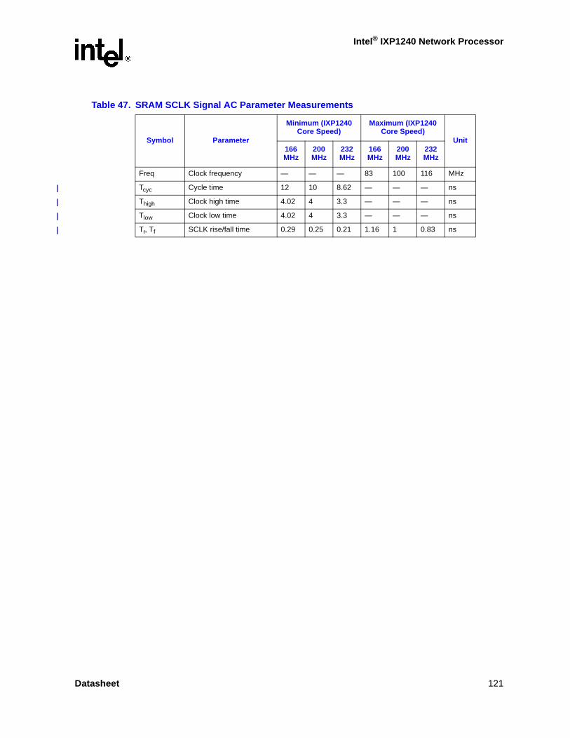
Intel® IXP1240 Network Processor
Table 47. SRAM SCLK Signal AC Parameter Measurements
Symbol Parameter
Minimum (IXP1240 Core Speed)
Maximum (IXP1240 Core Speed)
Unit166 MHz
200 MHz
232 MHz
166 MHz
200 MHz
232 MHz
Freq Clock frequency — — — 83 100 116 MHz
Tcyc Cycle time 12 10 8.62 — — — ns
Thigh Clock high time 4.02 4 3.3 — — — ns
Tlow Clock low time 4.02 4 3.3 — — — ns
Tr, Tf SCLK rise/fall time 0.29 0.25 0.21 1.16 1 0.83 ns
Datasheet 121
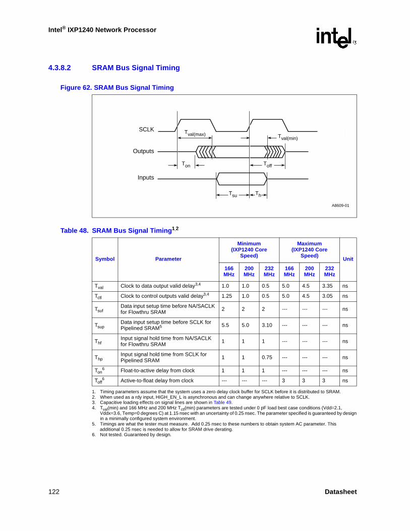
Intel® IXP1240 Network Processor
4.3.8.2 SRAM Bus Signal Timing
Figure 62. SRAM Bus Signal Timing
Table 48. SRAM Bus Signal Timing1,2
1. Timing parameters assume that the system uses a zero delay clock buffer for SCLK before it is distributed to SRAM.2. When used as a rdy input, HIGH_EN_L is asynchronous and can change anywhere relative to SCLK.
Symbol Parameter
Minimum(IXP1240 Core
Speed)
Maximum(IXP1240 Core
Speed)Unit
166 MHz
200 MHz
232 MHz
166 MHz
200 MHz
232 MHz
Tval Clock to data output valid delay3,4
3. Capacitive loading effects on signal lines are shown in Table 49.4. Tval(min) and 166 MHz and 200 MHz Tctl(min) parameters are tested under 0 pF load best case conditions (Vdd=2.1,
Vddx=3.6, Temp=0 degrees C) at 1.15 nsec with an uncertainty of 0.25 nsec. The parameter specified is guaranteed by designin a minimally configured system environment.
1.0 1.0 0.5 5.0 4.5 3.35 ns
Tctl Clock to control outputs valid delay3,4 1.25 1.0 0.5 5.0 4.5 3.05 ns
TsufData input setup time before NA/SACLK for Flowthru SRAM 2 2 2 --- --- --- ns
TsupData input setup time before SCLK for Pipelined SRAM5
5. Timings are what the tester must measure. Add 0.25 nsec to these numbers to obtain system AC parameter. This additional 0.25 nsec is needed to allow for SRAM drive derating.
5.5 5.0 3.10 --- --- --- ns
ThfInput signal hold time from NA/SACLK for Flowthru SRAM 1 1 1 --- --- --- ns
ThpInput signal hold time from SCLK for Pipelined SRAM 1 1 0.75 --- --- --- ns
Ton6
6. Not tested. Guaranteed by design.
Float-to-active delay from clock 1 1 1 --- --- --- ns
Toff6 Active-to-float delay from clock --- --- --- 3 3 3 ns
A8609-01
Tval(max)
Tsu Th
Tval(min)
Ton Toff
SCLK
Outputs
Inputs
122 Datasheet

Intel® IXP1240 Network Processor
Table 49. Signal Delay Deratings for Tval and Tctl
Signal Maximum Derating (ns/pF)(IX Bus Speed)
Minimum Derating (ns/pF)(IX Bus Speed)
83 MHz 100 MHz 116 MHz 83 MHz 100 MHz 116 MHz
SCLK 0.053 — — 0.025 — —
SLOW_EN_L 0.065 0.06 0.031 0.03 0.025 0.015
SWE_L 0.065 0.06 0.031 0.03 0.025 0.015
MRD_L 0.065 0.06 0.031 0.03 0.025 0.015
FWE_L 0.065 0.06 0.031 0.03 0.025 0.015
MCE_L 0.065 0.06 0.031 0.03 0.025 0.015
SOE_L 0.065 0.06 0.031 0.03 0.025 0.015
HIGH_EN_L 0.065 0.06 0.031 0.03 0.025 0.015
LOW_EN_L 0.065 0.06 0.031 0.03 0.025 0.015
CE_L[3:0] 0.065 0.06 0.031 0.03 0.025 0.015
A[18:0] 0.065 0.06 0.031 0.03 0.025 0.015
DQ[31:0] 0.065 0.06 0.031 0.03 0.025 0.015
Datasheet 123

Intel® IXP1240 Network Processor
4.3.8.3 SRAM Bus - SRAM Signal Protocol and Timing
Figure 63. Pipelined SRAM Read Burst of Eight Longwords
A8610-01
SCLK
SLOW_EN_L
MRD_L
FWE_L
SWE_L
SOE_L
CE_L<3:0> = 1110
A0 A1 A2 A3 A4 A5 A6 A7
D(A0) D(A1) D(A2) D(A3) D(A4) D(A5) D(A6) D(A7)
A[18:0]
DQ[31:0]
HIGH_EN_L
LOW_EN_L
CE_L[3:0]
124 Datasheet

Intel® IXP1240 Network Processor
Figure 64. Pipelined SRAM Write Burst of Eight Longwords
A8611-01
SCLK
SWE_L
SOE_L
SLOW_EN_L
MRD_L
FWE_L
A7A6A5A4A3A2A1A0
D(A1) D(A2) D(A3) D(A4) D(A5) D(A6) D(A7)D(A0)
A[18:0]
DQ[31:0]
HIGH_EN_L
LOW_EN_L
CE_L[3:0] CE_L<3:0> = 1110
Datasheet 125
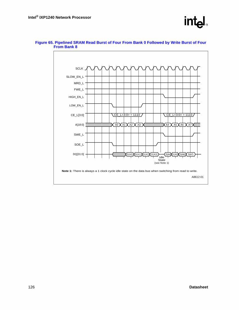
Intel® IXP1240 Network Processor
Figure 65. Pipelined SRAM Read Burst of Four From Bank 0 Followed by Write Burst of Four From Bank 8
A8612-01
SCLK
SWE_L
SOE_L
SLOW_EN_L
MRD_L
FWE_L
IdleState
(see Note 1)
A7A6A5A4A3A2A1A0
D(A4) D(A5) D(A6) D(A7)D(A0) D(A1)
CE_L<3:0> = 1110 CE_L<3:0> = 1110
D(A2) D(A3)
Note 1: There is always a 1 clock cycle idle state on the data bus when switching from read to write.
A[18:0]
DQ[31:0]
HIGH_EN_L
LOW_EN_L
CE_L[3:0]
126 Datasheet
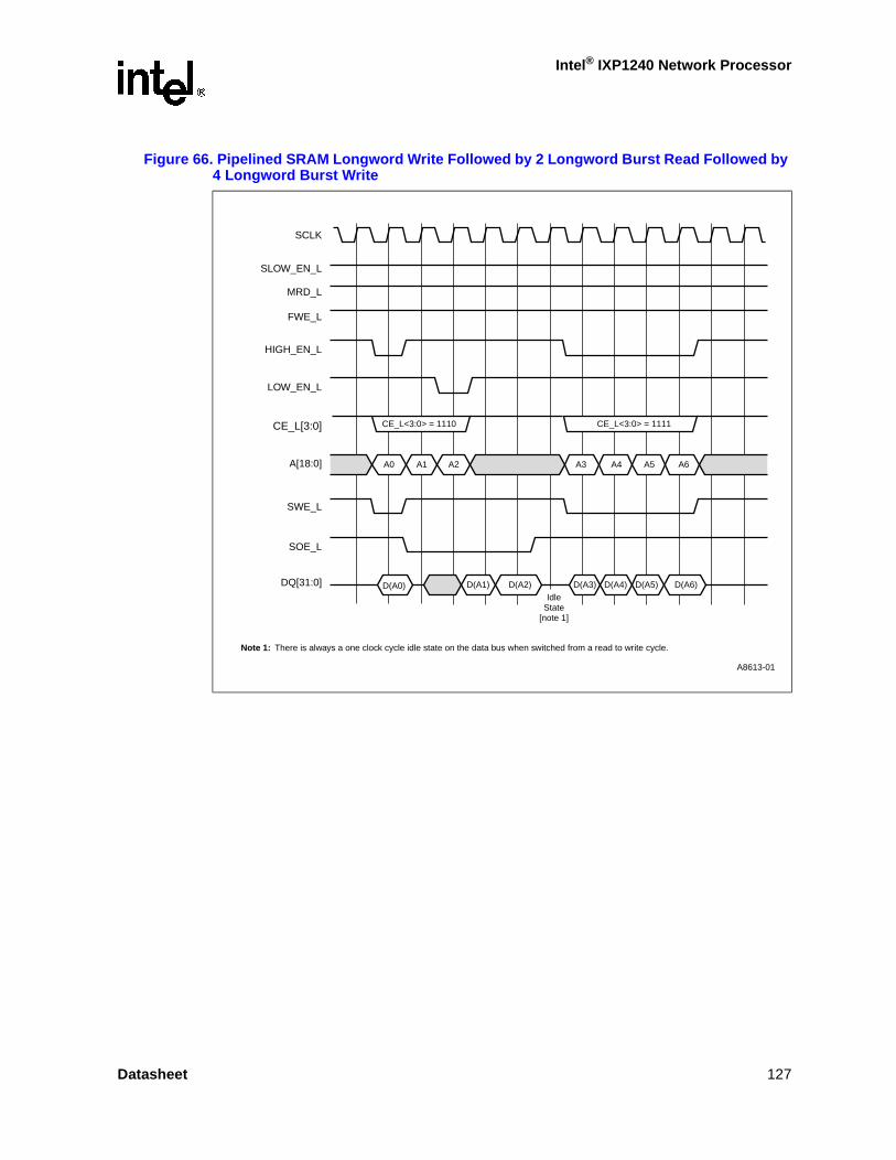
Intel® IXP1240 Network Processor
Figure 66. Pipelined SRAM Longword Write Followed by 2 Longword Burst Read Followed by 4 Longword Burst Write
A8613-01
SCLK
SLOW_EN_L
MRD_L
FWE_L
SWE_L
SOE_L
CE_L<3:0> = 1110 CE_L<3:0> = 1111
A0 A1 A2 A3 A4 A5 A6
D(A1) D(A2) D(A3)Idle
State[note 1]
Note 1: There is always a one clock cycle idle state on the data bus when switched from a read to write cycle.
D(A4) D(A5) D(A6)D(A0)
A[18:0]
DQ[31:0]
HIGH_EN_L
LOW_EN_L
CE_L[3:0]
Datasheet 127
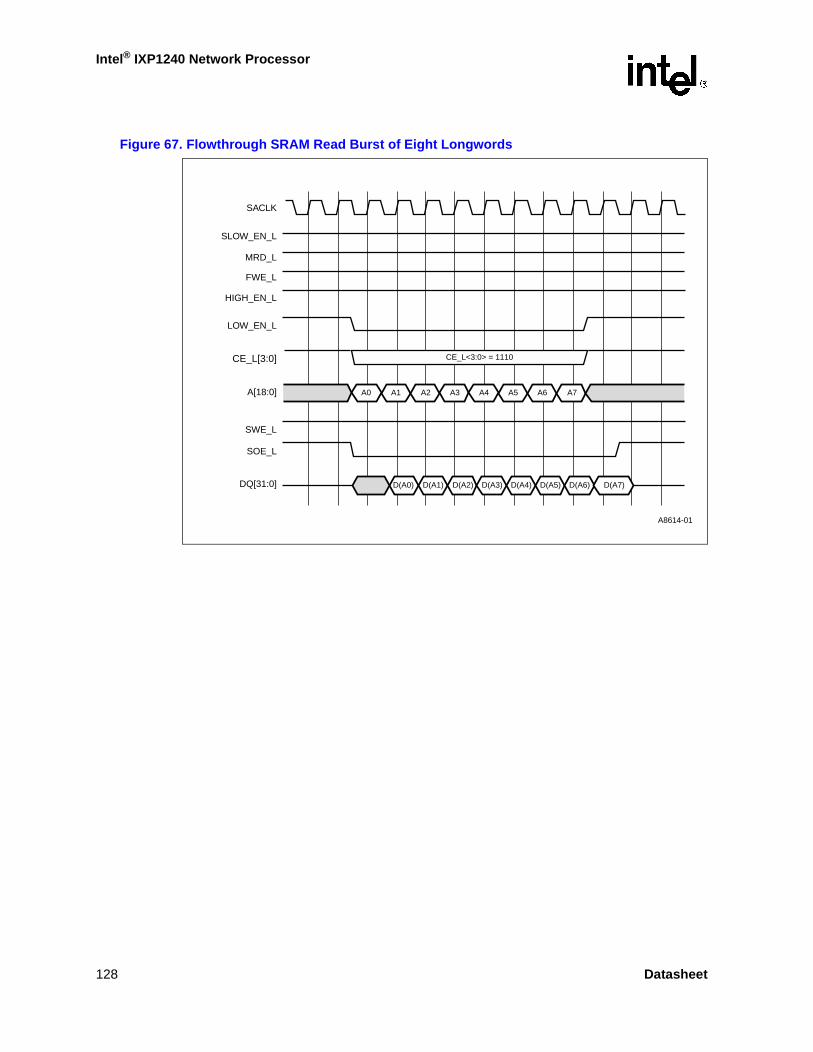
Intel® IXP1240 Network Processor
Figure 67. Flowthrough SRAM Read Burst of Eight Longwords
A8614-01
SACLK
SLOW_EN_L
MRD_L
FWE_L
SWE_L
SOE_L
CE_L<3:0> = 1110
A0 A1 A2 A3 A4 A5 A6 A7
D(A0) D(A1) D(A2) D(A3) D(A4) D(A5) D(A6) D(A7)
A[18:0]
DQ[31:0]
HIGH_EN_L
LOW_EN_L
CE_L[3:0]
128 Datasheet
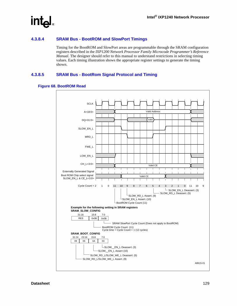
Intel® IXP1240 Network Processor
4.3.8.4 SRAM Bus - BootROM and SlowPort Timings
Timing for the BootROM and SlowPort areas are programmable through the SRAM configuration registers described in the IXP1200 Network Processor Family Microcode Programmer’s Reference Manual. The designer should refer to this manual to understand restrictions in selecting timing values. Each timing illustration shows the appropriate register settings to generate the timing shown.
4.3.8.5 SRAM Bus - BootRom Signal Protocol and Timing
Figure 68. BootROM Read
A8615-01
2 1 0 11 10 9 8 7 6 5 4 3 2 1 0 11
Example for the following setting in SRAM registersSRAM_SLOW_CONFIG
SLOW__EN_L Deassert. (3)
SLOW__EN_L Assert (10)
SLOW_RD_L/SLOW_WE_L Deassert. (5)
SLOW_RD_L/SLOW_WE_L Assert. (9)
10Cycle Count = 9
BootROM Cycle Count (11)Cycle time = Cycle Count + 1 (12 cycles)
Boot ROM Chip select signal SLOW_EN_L & CE_L<3:0>
Externally Generated Signal
BootROM Cycle Count (11)SLOW_EN_L Assert. (10)
SLOW_RD_L Assert. (9)SLOW_RD_L Deassert. (5)
SLOW_EN_L Deassert. (3)
7:015:831:16
RES
7:015:823:1631:24
09 05
0x0B 0x0B
SRAM_BOOT_CONFIG
0A 03
SRAM SlowPort Cycle Count (Does not apply to BootROM)
Valid CE
Valid Address
Valid CE
Valid
SCLK
A<18:0>
DQ<31:0>
SLOW_EN_L
MRD_L
FWE_L
LOW_EN_L
CH_L<3:0>
Datasheet 129

Intel® IXP1240 Network Processor
Figure 69. BootROM Write
A8616-01
2 1 0 11 10 9 8 7 6 5 4 3 2 1 0 11
Example for the following setting in SRAM registersSRAM_SLOW_CONFIG
10Cycle Count = 9
BootROM Cycle Count (11)Cyele time= Cycle Count + 1 (12 cycles)
BootROM Chip select signalSLOW_EN_L or CE_L<3:0>
Externally Generated Signal
BootROM Cycle Count (11)SLOW_EN_L Assert. (10)
SLOW_WE_L Assert. (9)SLOW_WE_L Deassert. (5)
SLOW_EN_L Deassert. (3)
7:015:831:16
RES 0x0B 0x0B
SRAM SlowPort Cycle Count (Does not apply to BootROM)
Valid CE
Valid Address
Valid Data
Valid CE
SCLK
SLOW_EN_L
MRD_L
FWE_L
SLOW__EN_L Deassert. (3)
SLOW__EN_L Assert (10)
SLOW_RD_L/SLOW_WE_L Deassert. (5)
SLOW_RD_L/SLOW_WE_L Assert. (9)
7:015:823:1631:24
09 0A
SRAM_BOOT_CONFIG
05 03
A[18:0]
DQ[31:0]
HIGH_EN_L
LOW_EN_L
CE_L[3:0]
130 Datasheet
Intel® IXP1240 Network Processor
Figure 70. Pipelined SRAM Two Longword Burst Read Followed by BootROM Write
A8617-01
A[18:0] A1 A2 A3A3
DQ[31:0] D(A1) D(A2)D(A1) D(A3)D(A3)
Buffered DQ[31:0] D(A3)D(A3)
SLOW_EN_L
MRD_L
FWE_L
HIGH_EN_L
LOW_EN_L
CE_L[3:0] CE_L<3:0> = 1110
SCLK
BootROM_CE_L[3:0]BootROM_CE_L = -(-SLOW_EN_L & -CE_L)
SWE_L
SOE_L
Datasheet 131
Intel® IXP1240 Network Processor
4.3.8.6 SRAM Bus - Slow-Port Device Signal Protocol and Timing
Figure 71. SRAM SlowPort Read
A8618-01
SCLK
A[18:0]
DQ[31:0]
SLOW_EN_L
MRD_L
FWE_L
LOW_EN_L
HIGH_EN_L
MCE_L
2 1 0 11 10 9 8 7 6 5 4 3 2 1 0 11
Example for the following setting in SRAM registersSRAM_SLOW_CONFIG
Cycle time = Cycle Count + 1 (12 cycles)
10Cycle Count = 9
BootROM Cycle Count (Does not apply to SRAM SlowPort)
SRAM SlowPort Chip select signal - MCE_L & address
Externally Generated Signal
BootROM Cycle Count (11)MCE_L/SLOW_EN_L Assert. (10)
SLOW_RD_L Assert. (9)SLOW_RD_L Deassert. (5)
SLOW_EN_L Deassert. (3)
7:015:831:16
RES 0x0B 0x0B
SRAM Slow Port Cycle Count (11)
Valid CE
Valid Address
Valid
SLOW__EN_L Deassert. (3)
SLOW__EN_L Assert (10)
SLOW_RD_L/SLOW_WE_L Deassert. (5)
SLOW_RD_L/SLOW_WE_L Assert. (9)
7:015:823:1631:24
09 0A
SRAM_SLOWPORT_CONFIG
05 03
132 Datasheet

Intel® IXP1240 Network Processor
Figure 72. SRAM SlowPort Write
A8619-01
2 1 0 11 10 9 8 7 6 5 4 3 2 1 0 11
Example for the following setting in SRAM registersSRAM_SLOW_CONFIG
Cycle time = Cycle Count + 1 (12 cycles)
10Cycle Count = 9
BootROM Cycle Count (Does not apply to SRAM SlowPort)
SRAM SlowPort Chip select signal - MCE_L & address
Externally Generated Signal
BootROM Cycle Count (11)MCE_L/SLOW_EN_L Assert. (10)
SLOW_WR_L Assert. (9)SLOW_RD_L Deassert. (5)
SLOW_EN_L Deassert. (3)
7:015:831:16
RES 0x0B 0x0B
SRAM SlowPort Cycle Count (11)
Valid CE
Valid Address
Valid Data
SCLK
A[18:0]
DQ[31:0]
SLOW_EN_L
MRD_L
FWE_L
LOW_EN_L
HIGH_EN_L
MCE_L
SLOW__EN_L Deassert. (3)
SLOW__EN_L Assert (10)
SLOW_RD_L/SLOW_WE_L Deassert. (5)
SLOW_RD_L/SLOW_WE_L Assert. (9)
7:015:823:1631:24
09 0A
SRAM_SLOWPORT_CONFIG
05 03
Datasheet 133

Intel® IXP1240 Network Processor
Figure 73. SRAM SlowPort
A8620-01
Register Settings used for these timings:SRAM_SLOW_CONFIG=000A:0B0Fh where RDY_L Pause State=Ah, BCC=0Bh, and SCC=0FhSRAM_SLOWPORT_CONFIG=0D0E:0501h where SRWA=0Dh, SCEA=0Eh, SRWD=05h, SCED=01SRAM_CSR=0009:4810h where <19>=1, RDY_L enabled
Cycle_count loadcount Fh Eh Dh Ch Bh Ah Ah Ah Ah Ah Ah Ah 9 8 7 6 5 6 3 2 1 0
RDY_L_Pause_State value=(SRWD+5) minimumadditional
wait statesRDY_L pausestate=Ah
ext_CE_L(MCE_L.AND.Ax)
MCE_L
LOW_EN_L
HIGH_EN_L
2 SCLKs Minimum
RDY# input sampled asynchronously while waitingin internal pause state A
FWE_L
MRD_L
SLOW_EN_L
DQ[31:0]
A[18:0]
SCLK
134 Datasheet
Intel® IXP1240 Network Processor
Figure 74. Pipelined SRAM Two Longword Burst Read Followed By SlowPort Write
A8621-01
SCLK
A[18:0] A1 A2 A3A3
DQ[31:0] D(A2)D(A1)
Buffered DQ[31:0]
D(A3)D(A3)
D(A3)D(A3)
MCE_L
MRD_L
FWE_L
HIGH_EN_L
LOW_EN_L
CE_L[3:0]
SWE_L
SOE_L
CE_L<3:0> = 1110
SLOW_EN_L
BootROM_CE_L[3:0]
Datasheet 135
Intel® IXP1240 Network Processor
4.3.9 SDRAM Interface
4.3.9.1 SDCLK AC Parameter Measurements
Vt1 = 0.5*VDDXVt2 = 0.4*VDDXVt3 = 0.3*VDDX
Figure 75. SDCLK AC Timing Diagram
A8622-01
Tcyc
TfTr
Vt3
Vt1
Vt2
Thigh
Tlow
Table 50. SDCLK AC Parameter Measurements
Symbol Parameter
Minimum (IXP1240 Core Speed)
Maximum (IXP1240 Core Speed)
Unit166 MHz
200 MHz
232 MHz
166 MHz
200 MHz
232 MHz
Freq Clock frequency — — — 83 100 116 MHz
Tcyc Cycle time 12 10 8.62 — — — ns
Thigh Clock high time 4.02 4 3.3 — — — ns
Tlow Clock low time 4.02 4 3.3 — — — ns
Tr, Tf SDCLK rise/fall time 0.29 0.25 0.21 1.16 1 0.83 ns
136 Datasheet

Intel® IXP1240 Network Processor
4.3.9.2 SDRAM Bus Signal Timing
Figure 76. SDRAM Bus Signal Timing
Table 51. SDRAM Bus Signal Timing Parameters1
1. Timing parameters assume that the system uses a zero delay clock buffer for SDCLK before it is distributed to SDRAM.
Symbol Parameter
Minimum(IXP1240 Core
Speed)
Maximum(IXP1240 Core
Speed)Unit
166 MHz
200 MHz
232 MHz
166 MHz
200 MHz
232 MHz
Tval Clock to data output valid delay2,3
2. Capacitive loading effects on signal lines are shown in Table 52.3. Tval(min) and 166 MHz and 200 MHz Tctl(min) parameters are tested under 0 pF load best case conditions (Vdd=2.1,
Vddx=3.6, Temp=0 degrees C) at 1.15 nsec with an uncertainty of 0.25 nsec. The parameter specified is guaranteed by designin a minimally configured system environment.
1.25 1.0 0.5 4.5 4.0 3.3 ns
Tctl SDCLK to control output valid delay2,3 1.25 1.0 0.5 4.5 4.0 2.90 ns
Tsu Data input setup time before SDCLK4
4. Unlike the SRAM setup timing parameterTsup, the Tsu timings are both what the tester must measure and what the SDRAM parts will deliver. Increased performance on the SDRAM bus occurs because the data pins only drive one load.
4.25 3.70 3.70 --- --- --- ns
Th Data input hold time from SDCLK 1 1 0.75 --- --- --- ns
Ton5
5. Not tested. Guaranteed by design.
Float to data driven delay from SDCLK 1.25 1 0.75 --- --- --- ns
Toff5 Data driven to float delay from SDCLK --- --- --- 3 3 3 ns
A8905-01
Tval(max)
Tsu Th
Tval(min)
Ton
Tctl(max) Tctl(min)
Toff
SDCLK
MDATA (output)
MDATA (input)
Control Outputs(RAS_L, CAS_L,
WE_L, DQM, MADR)
Datasheet 137
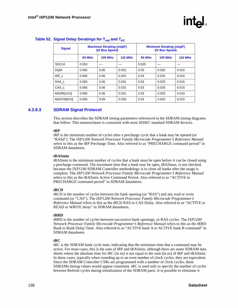
Intel® IXP1240 Network Processor
4.3.9.3 SDRAM Signal Protocol
This section describes the SDRAM timing parameters referenced in the SDRAM timing diagrams that follow. This nomenclature is consistent with most JEDEC standard SDRAM devices.
tRPtRP is the minimum number of cycles after a precharge cycle that a bank may be opened (or "RASd"). The IXP1200 Network Processor Family Microcode Programmer’s Reference Manual refers to this as the tRP Precharge Time. Also referred to as “PRECHARGE command period” in SDRAM datasheets.
tRASmintRASmin is the minimum number of cycles that a bank must be open before it can be closed using a precharge command. The maximum time that a bank may be open, tRASmax, is not checked, because the IXP1240 SDRAM Controller methodology is to close all banks after the usage is complete. The IXP1200 Network Processor Family Microcode Programmer’s Reference Manual refers to this as the tRASmin Active Command Period. Also referred to as “ACTIVE to PRECHARGE command period” in SDRAM datasheets.
tRCDtRCD is the number of cycles between the bank opening (or "RAS") and any read or write command (or "CAS"). The IXP1200 Network Processor Family Microcode Programmer’s Reference Manual refers to this as the tRCD RAS to CAS Delay. Also referred to as “ACTIVE to READ or WRITE delay” in SDRAM datasheets.
tRRDtRRD is the number of cycles between successive bank openings, or RAS cycles. The IXP1200 Network Processor Family Microcode Programmer’s Reference Manual refers to this as the tRRD Bank to Bank Delay Time. Also referred to as “ACTIVE bank A to ACTIVE bank B command” in SDRAM datasheets.
tRCtRC is the SDRAM bank cycle time, indicating that the minimum time that a command may be active. For most cases, this is the sum of tRP and tRASmin, although there are some SDRAM data sheets where the absolute time for tRC (in ns) is not equal to the sum (in ns) of tRP and tRASmin. In these cases, typically when rounding up to an even number of clock cycles, they are equivalent. Since the SDRAM Controller CSRs are programmed with a number of clock cycles, these SDRAMs timing values would appear consistent. tRC is used only to specify the number of cycles between Refresh cycles during initialization of the SDRAM parts. It is possible to eliminate it
Table 52. Signal Delay Deratings for Tval and Tctl
Signal Maximum Derating (ns/pF)(IX Bus Speed)
Minimum Derating (ns/pF)(IX Bus Speed)
83 MHz 100 MHz 116 MHz 83 MHz 100 MHz 116 MHz
SDCLK 0.053 — — 0.025 — —
DQM 0.065 0.06 0.031 0.03 0.025 0.015
WE_L 0.065 0.06 0.031 0.03 0.025 0.015
RAS_L 0.065 0.06 0.031 0.03 0.025 0.015
CAS_L 0.065 0.06 0.031 0.03 0.025 0.015
MADR[14:0] 0.065 0.06 0.031 0.03 0.025 0.015
MDATA[63:0] 0.095 0.09 0.035 0.03 0.025 0.015
138 Datasheet
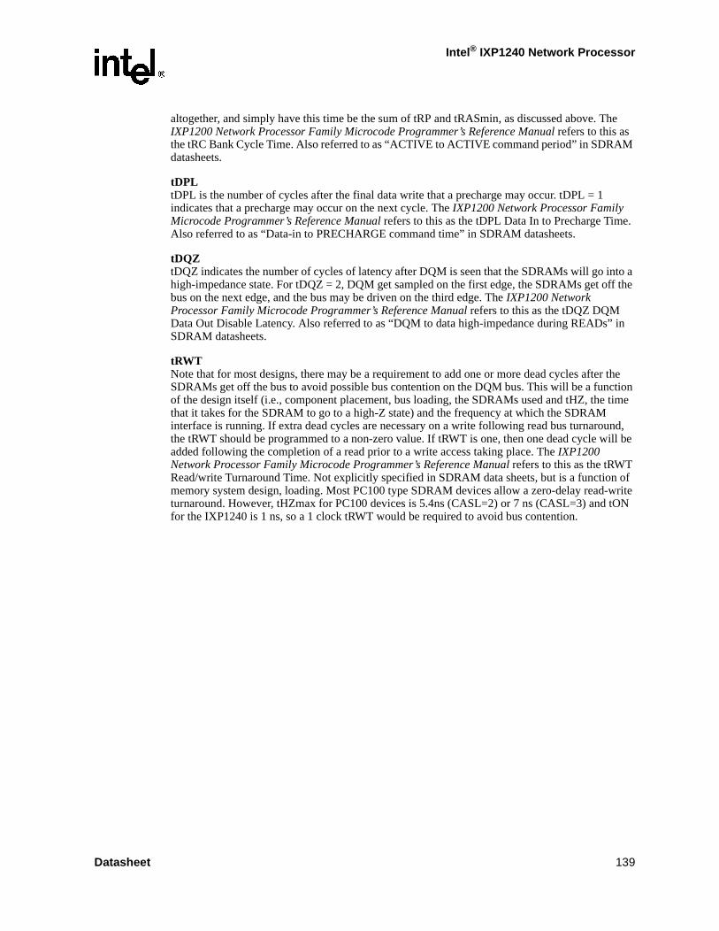
Intel® IXP1240 Network Processor
altogether, and simply have this time be the sum of tRP and tRASmin, as discussed above. The IXP1200 Network Processor Family Microcode Programmer’s Reference Manual refers to this as the tRC Bank Cycle Time. Also referred to as “ACTIVE to ACTIVE command period” in SDRAM datasheets.
tDPLtDPL is the number of cycles after the final data write that a precharge may occur. tDPL = 1 indicates that a precharge may occur on the next cycle. The IXP1200 Network Processor Family Microcode Programmer’s Reference Manual refers to this as the tDPL Data In to Precharge Time. Also referred to as “Data-in to PRECHARGE command time” in SDRAM datasheets.
tDQZtDQZ indicates the number of cycles of latency after DQM is seen that the SDRAMs will go into a high-impedance state. For tDQZ = 2, DQM get sampled on the first edge, the SDRAMs get off the bus on the next edge, and the bus may be driven on the third edge. The IXP1200 Network Processor Family Microcode Programmer’s Reference Manual refers to this as the tDQZ DQM Data Out Disable Latency. Also referred to as “DQM to data high-impedance during READs” in SDRAM datasheets.
tRWTNote that for most designs, there may be a requirement to add one or more dead cycles after the SDRAMs get off the bus to avoid possible bus contention on the DQM bus. This will be a function of the design itself (i.e., component placement, bus loading, the SDRAMs used and tHZ, the time that it takes for the SDRAM to go to a high-Z state) and the frequency at which the SDRAM interface is running. If extra dead cycles are necessary on a write following read bus turnaround, the tRWT should be programmed to a non-zero value. If tRWT is one, then one dead cycle will be added following the completion of a read prior to a write access taking place. The IXP1200 Network Processor Family Microcode Programmer’s Reference Manual refers to this as the tRWT Read/write Turnaround Time. Not explicitly specified in SDRAM data sheets, but is a function of memory system design, loading. Most PC100 type SDRAM devices allow a zero-delay read-write turnaround. However, tHZmax for PC100 devices is 5.4ns (CASL=2) or 7 ns (CASL=3) and tON for the IXP1240 is 1 ns, so a 1 clock tRWT would be required to avoid bus contention.
Datasheet 139

Intel® IXP1240 Network Processor
Figure 77. SDRAM Initialization Sequence
A8624-01
tRP
INIT_DLY
Prechargeall banks
Mode RegisterSet Command
AutoRefresh
AutoRefresh
SDCLK
RAS_L
CAS_L
WE_L
MADR
MDAT
DQM
(see note 2)(see note 1)
Notes:1. Number of total initialization phase refresh cycles programmed as INIT_RFRSH value in register SDRAM_MEMINIT.2. Burst length and CAS latency values programmed as BURSTL value in register SDRAM_MEMCTL0 emitted in this cycle.3. INIT_DLY, tRSC values programmed into register SDRAM_MEMINIT.4. tRP, tRC values programmed into register SDRAM_MEMCTL15. tRSC is minimum SDRAM programmable register value. In actual use, refresh cycles will notoccur immediately after tRSC cycles due to SDRAM unit internal pipeline delays.
tRc tRSC
140 Datasheet
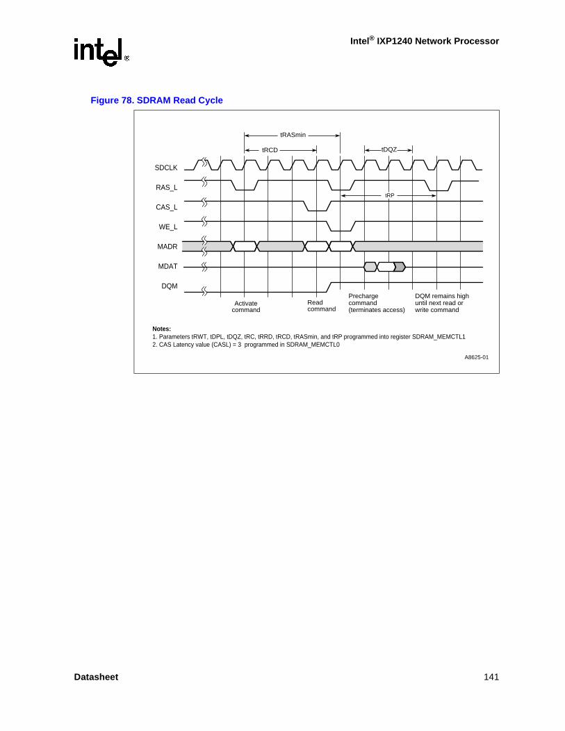
Intel® IXP1240 Network Processor
Figure 78. SDRAM Read Cycle
A8625-01
tRCD
tRASmin
tDQZ
SDCLK
RAS_L
CAS_L
WE_L
MADR
MDAT
DQM
Activatecommand
Readcommand
Prechargecommand(terminates access)
DQM remains highuntil next read orwrite command
tRP
Notes:1. Parameters tRWT, tDPL, tDQZ, tRC, tRRD, tRCD, tRASmin, and tRP programmed into register SDRAM_MEMCTL12. CAS Latency value (CASL) = 3 programmed in SDRAM_MEMCTL0
Datasheet 141

Intel® IXP1240 Network Processor
Figure 79. SDRAM Write Cycle
A8626-01
tRCD
tRASmin
tDPL
tRP
SDCLK
RAS_L
CAS_L
WE_L
MADR
MDAT
DQM
Activatecommand
Writecommand
Prechargecommand(terminates access)
DQM remains highuntil next read orwrite command
Notes:1. Parameters tRWT, tDPL, tDQZ, tRC, tRRD, tRCD, tRASmin, and tRP programmed into register SDRAM_MEMCTL12. CAS Latency value (CASL) = 3 programmed in SDRAM_MEMCTL0
142 Datasheet

Intel® IXP1240 Network Processor
4.4 Asynchronous Signal Timing Descriptions
RESET_IN_L Must remain asserted for 150 ms after VDD and VDDX are stable to properly reset the IXP1240.
RESET_OUT_LIs asserted for all types of reset (hard, watchdog, and software) and appears on the pin asynchronously to all clocks.
GPIO[3:0] Are read and written under software control. When writing a value to these pins, the pins transition approximately 20 ns after the write is performed. When reading these pins, the signal is first synchronized to the internal clock and must be valid for at least 20 ns before it is visible to a processor read.
TXD, RXD Are asynchronous relative to any device outside the IXP1240.
Figure 80. SDRAM Read-Modify-Write Cycle
A8627-01
SDCLK
RAS_L
CAS_L
WE_L
MADR
MDAT
DQM
Notes:1. Parameters tRWT, tDPL, tDQZ, tRC, tRRD, tRCD, tRASmin, and tRP programmed into register SDRAM_MEMCTL12. CAS Latency value (CASL) = 3 programmed in SDRAM_MEMCTL0
tRCD
tRASmin
Activatecommand
Readcommand
Writecommand
Prechargecommand
DQM remains highduring modify
DQM remains highuntil next read orwrite command
tDQZ tRWT
tDPL
Datasheet 143

Intel® IXP1240 Network Processor
5.0 Mechanical Specifications
5.1 Package Dimensions
The IXP1240 is contained in a 432-HL-PBGA package, as shown in the following illustrations.
Figure 81. IXP1240 Part Marking
A8906-02
Pin 1
i GCIXP1240xxFFFFFFFFINTEL M C 2001
xxxxxxxSzYWW PHILLIPPINES
BSMC(ALT# & DATE CODE, COO)
FPO # Intel Legal
Name
144 Datasheet

Intel® IXP1240 Network Processor
Figure 82. 432-Pin HL-PBGA Package - Bottom View
Figure 83. IXP1240 Side View
Figure 84. IXP1240 A-A Section View
A7063-02
S
A
A
S e
b0
e
0.30 A C A S A S
D
26 25 24 23 2231 30 29 28 27 21 20 19 18 17 16 15 14 13 12 11 10 9 8 7 6 5 4 3 12
E
D1
E1
A1Ball
Corner
A
BC
DEF
GH
JK
LMN
PR
TU
AEAF
V
W
AAABAC
AD
AKAL
AGAHAJ
Y
A7064-01
A
A1
A2
bbb C ccc
Seating Plane
aaa –C–
A7043-01
dddd
P
Datasheet 145
Intel® IXP1240 Network Processor
5.2 IXP1240 Package Dimensions (mm)
Table 53. IXP1240 Package Dimensions (mm)
Symbol Definition Minimum Nominal Maximum
A Overall thickness 1.41 1.54 1.67
A1 Ball height 0.56 0.63 0.70
A2 Body thickness 0.85 0.91 0.97
D Body size 39.90 40.00 40.10
D1 Ball footprint 38.00 38.10 38.20
E Body size 39.90 40.00 40.10
E1 Ball footprint 38.00 38.10 38.20
b Ball diameter 0.60 0.75 0.90
aaa Coplanarity -- -- 0.20
bbb Parallel -- -- 0.15
ccc Top flatness -- -- 0.20
ddd [8] Seating plane clearance 0.15 0.33 0.50
P Encapsulation height 0.20 0.30 0.35
S Solder ball placement -- -- 0.00
M, N Ball matrix -- 31 x 31 --
M1[7] Number of rows deep -- 4 --
d Minimum distance, encap to balls -- 0.6 --
e Ball pitch -- 1.27 --
NOTES:1. All dimensions and tolerances conform to ANSI Y1.45M-1982.2. Dimension “b” is measured at the maximum solder ball diameter parallel to primary datum “c”.3. Primary datum “c” and seating plane are defined by the spherical crowns of the solder balls.4. Pin A1 I.D. marked by ink.5. Shape at corner, single form.6. All dimensions are in millimeters.7. Number of rows in from edge to center.8. Height from ball seating plane to plane of encapsulant.9. S is measured with respect to -A- and -B- and defines the position of the center solder ball in the outer row.
When there is an odd number of solder balls in the outer row, S=0.000; when there is an even number of solder balls in the outer row, the value S=e/2. S can be either 0.000 or e/2 for each variation.
10.The dimension from the outer edge of the resin dam to the edge of the innermost row of the solder ball pads is to be a minimum of 0.50 mm.
146 Datasheet