intel® quark se microcontroller c1000 assumptions intel® quark se microcontroller c1000 platform...
TRANSCRIPT
Document Number: 334715-004EN
Intel® Quark™ SE Microcontroller C1000
Platform Design Guide
June 2017
Intel® Quark™ SE Microcontroller C1000
Platform Design Guide June 2017
2 Document Number: 334715-004EN
You may not use or facilitate the use of this document in connection with any infringement or other legal analysis concerning Intel products
described herein. You agree to grant Intel a non-exclusive, royalty-free license to any patent claim thereafter drafted which includes subject
matter disclosed herein.
No license (express or implied, by estoppel or otherwise) to any intellectual property rights is granted by this document.
All information provided here is subject to change without notice. Contact your Intel representative to obtain the latest Intel product
specifications and roadmaps.
The products described may contain design defects or errors known as errata which may cause the product to deviate from published
specifications. Current characterized errata are available on request.
Copies of documents which have an order number and are referenced in this document may be obtained by calling 1-800-548-4725 or by
visiting: http://www.intel.com/design/literature.htm
Intel technologies’ features and benefits depend on system configuration and may require enabled hardware, software or service activation.
Learn more at http://www.intel.com/ or from the OEM or retailer.
No computer system can be absolutely secure.
Intel, Quark, and the Intel logo are trademarks of Intel Corporation in the U.S. and/or other countries.
*Other names and brands may be claimed as the property of others.
Copyright © 2017, Intel Corporation. All rights reserved.
Intel® Quark™ SE Microcontroller C1000
June 2017 Platform Design Guide
Document Number: 334715-004EN 3
Contents
1.0 Introduction ................................................................................................................................................. 8
1.1 Overview ................................................................................................................................................................ 8
1.2 Audience and Purpose .................................................................................................................................... 8
1.3 Terminology ......................................................................................................................................................... 9
1.4 Reference Documents ..................................................................................................................................... 9
2.0 System Assumptions ...............................................................................................................................10
2.1 General Assumptions .................................................................................................................................... 10
2.1.1 PCB Technology and Stackup ................................................................................................ 11 2.1.2 PCB Technology Considerations .......................................................................................... 11
2.2 Backward and Forward Coupling Coefficient Calculation ............................................................ 13 2.3 Feature Set ........................................................................................................................................................ 14
2.4 Pin Mapping ...................................................................................................................................................... 15
3.0 Subsystem Details ....................................................................................................................................23
3.1 Design Recommendations .......................................................................................................................... 23
3.2 General Design Guideline Assumptions ............................................................................................... 24
4.0 I2C Interface ...............................................................................................................................................25
4.1 I2C Interfaces Signals .................................................................................................................................... 25 4.2 Interface Routing Guidelines ..................................................................................................................... 25
5.0 Pulse Width Modulation (PWM) ............................................................................................................28
5.1 PWM Signaling ................................................................................................................................................. 28
5.2 Functional Operation .................................................................................................................................... 29
6.0 UART ...........................................................................................................................................................31
6.1 Signal Descriptions ........................................................................................................................................ 31
6.2 Features .............................................................................................................................................................. 32
7.0 SPI ................................................................................................................................................................34
7.1 Signal Descriptions ........................................................................................................................................ 34
7.2 Features .............................................................................................................................................................. 37
8.0 Clocking ......................................................................................................................................................39
8.1 Signal Descriptions ........................................................................................................................................ 39
8.2 Features .............................................................................................................................................................. 41
9.0 General Purpose I/O (GPIO) ...................................................................................................................42
9.1 Signal Descriptions ........................................................................................................................................ 42
9.2 Features .............................................................................................................................................................. 43
10.0 JTAG ............................................................................................................................................................44
10.1 Signal Descriptions ........................................................................................................................................ 44
Intel® Quark™ SE Microcontroller C1000
Platform Design Guide June 2017
4 Document Number: 334715-004EN
10.2 Features .............................................................................................................................................................. 45
11.0 Analog-to-Digital Converter (ADC) .......................................................................................................46
11.1 Signal Descriptions ........................................................................................................................................ 46
11.2 Features .............................................................................................................................................................. 46
12.0 USB ..............................................................................................................................................................48
12.1 Signal Descriptions ........................................................................................................................................ 48
12.2 Features .............................................................................................................................................................. 49
13.0 Power ..........................................................................................................................................................51
13.1 Configuration for External VR ................................................................................................................... 51
13.2 Configuration for Internal VR .................................................................................................................... 53
14.0 Termination of Unused Pins ..................................................................................................................56
14.1 Guidelines for Terminating Unused Pins ............................................................................................. 56
14.2 Termination of Unused Pins for Intel® Quark™ SE Microcontroller C1000 ........................... 56
14.2.1 GPIO Pin Termination ................................................................................................................ 56 14.2.2 Sensor Subsystem SPI Pin Termination ............................................................................ 57 14.2.3 I2C Pin Termination ..................................................................................................................... 58 14.2.4 UART Pin Termination ............................................................................................................... 59 14.2.5 JTAG Pin Termination ................................................................................................................ 59 14.2.6 USB Pin Termination .................................................................................................................. 60 14.2.7 Pin Termination Summary ....................................................................................................... 60
Figures
Figure 1. Intel® Quark™ SE Microcontroller C1000 CRB Block Diagram .................................................... 10 Figure 2. SoC Block Diagram......................................................................................................................................... 11 Figure 3. Single-Ended Microstrip Diagram ........................................................................................................... 12 Figure 4. Differential-Microstrip Diagram ............................................................................................................... 12 Figure 5. Backward Coupling Coefficient ................................................................................................................ 13 Figure 6. Forward Coupling Coefficient ................................................................................................................... 14 Figure 7. Single-Ended Kb Diagram........................................................................................................................... 14 Figure 8. Differential Kb Diagram ............................................................................................................................... 14 Figure 9. SoC Interfaces .................................................................................................................................................. 16 Figure 10. I2C Point-to-Point Topology ...................................................................................................................... 26 Figure 11. Duty Cycle of 20% .......................................................................................................................................... 29 Figure 12. Duty Cycle of 50% .......................................................................................................................................... 29 Figure 13. Duty Cycle of 80% .......................................................................................................................................... 29 Figure 14. UART Point-to-Point Topology ................................................................................................................ 31 Figure 15. SPI Point-to-Point Single Flash Topology ........................................................................................... 34 Figure 16. SPI Point-to-Point Dual Flash Topology .............................................................................................. 35 Figure 17. SPI_CS Point-to-Point Dual Flash Topology ...................................................................................... 36 Figure 18. RTC Topology ................................................................................................................................................... 39
Intel® Quark™ SE Microcontroller C1000
June 2017 Platform Design Guide
Document Number: 334715-004EN 5
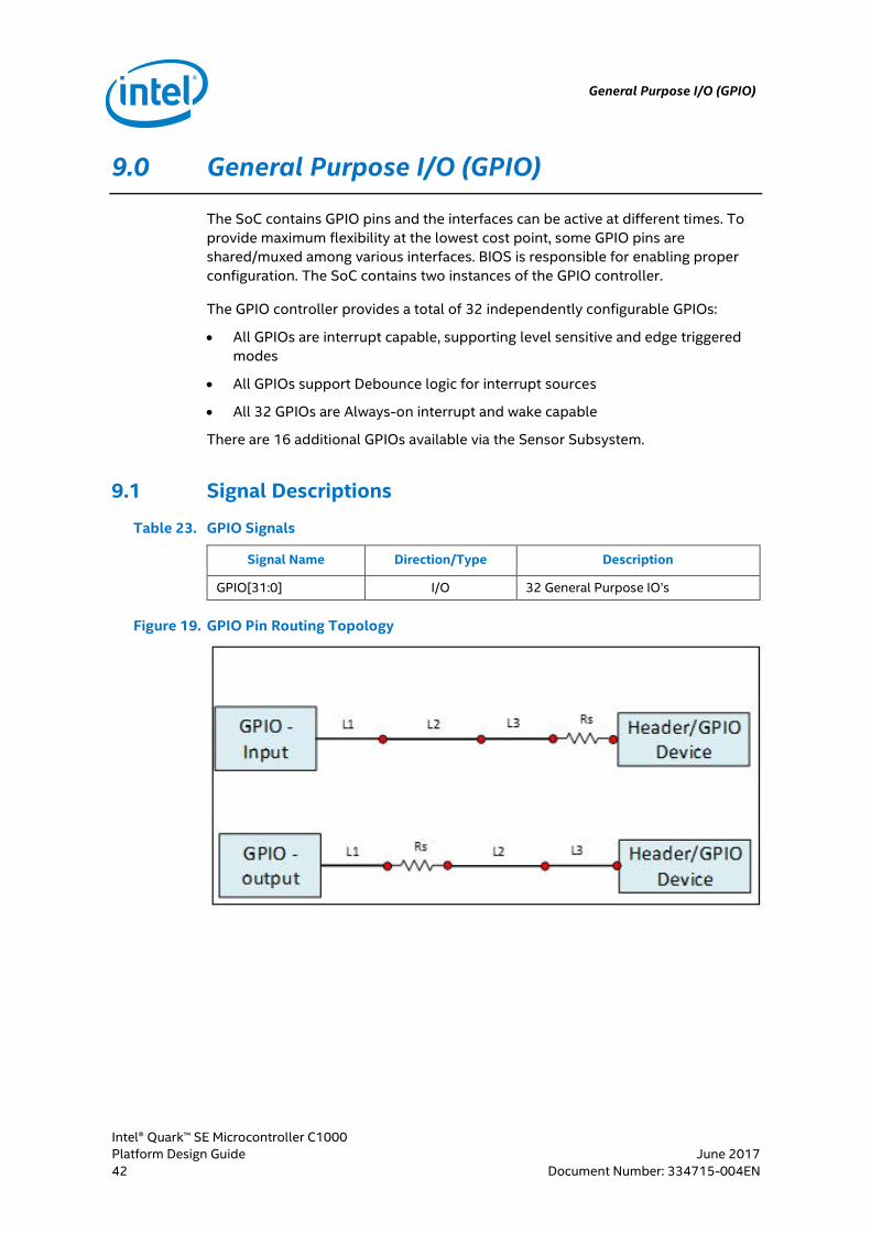
Figure 19. GPIO Pin Routing Topology ....................................................................................................................... 42 Figure 20. JTAG Topology ................................................................................................................................................ 44 Figure 21. Analog Shielding Requirement ................................................................................................................. 46 Figure 22. USB Topology .................................................................................................................................................. 48 Figure 23. USB Topology – Block Diagram ............................................................................................................... 48 Figure 24. Configuration for External VR ................................................................................................................... 52 Figure 25. Power Sequence for External Regulator .............................................................................................. 52 Figure 26. Power Timings for External Regulator .................................................................................................. 53 Figure 27. Power Delivered by an Internal 1.8V VR Only ................................................................................... 54 Figure 28. Power Sequence for Internal Regulator ............................................................................................... 55 Figure 29. GPIO Pin Termination Example (External Pull-Down Resistor) .................................................. 57 Figure 30. Sensor Subsystem SPI Pin Termination Example ............................................................................ 58 Figure 31. I2C Pin Termination Example ..................................................................................................................... 58 Figure 32. I2C Pin Termination Example (External Pull-up Resistor) ............................................................. 59 Figure 33. UART Pin Termination Example ............................................................................................................... 59 Figure 34. JTAG Pin Termination Example ............................................................................................................... 60 Figure 35. USB Pin Termination Example .................................................................................................................. 60
Tables
Table 1. Terminology ......................................................................................................................................................... 9 Table 2. Reference Documents ..................................................................................................................................... 9 Table 3. Stackup Details ................................................................................................................................................ 13 Table 4. Alphabetical Ball Listing for BGA package .......................................................................................... 16 Table 5. Good Layout Practices ................................................................................................................................. 24 Table 6. I2C Interface Signals....................................................................................................................................... 25 Table 7. I2C Point-to-Point Platform Routing Guidelines ............................................................................... 26 Table 8. Capacitance Estimates for Calculating Rpu Values ......................................................................... 27 Table 9. PWM Interface Signals ................................................................................................................................. 28 Table 10. PWM Timing ...................................................................................................................................................... 29 Table 11. Timer Period ..................................................................................................................................................... 30 Table 12. UART Signals .................................................................................................................................................... 31 Table 13. UART Point-to-Point Topology Platform Routing Guidelines .................................................... 32 Table 14. SPI Signals ......................................................................................................................................................... 34 Table 15. SPI Single Flash Platform Routing Guidelines ................................................................................... 34 Table 16. SPI Dual Flash Platform Routing Guidelines....................................................................................... 36 Table 17. SPI_CS Dual Flash Platform Routing Guidelines............................................................................... 37 Table 18. Clocking Signals .............................................................................................................................................. 39 Table 19. RTC Signals........................................................................................................................................................ 40 Table 20. RTC Point-to-Point Topology Platform Routing Guidelines ....................................................... 40 Table 21. 32Mhz Crystal Oscillator specification .................................................................................................. 40 Table 22. 32Khz Crystal Oscillator specification ................................................................................................... 41 Table 23. GPIO Signals ..................................................................................................................................................... 42 Table 24. GPIO Pin Routing Guidelines ..................................................................................................................... 43
Intel® Quark™ SE Microcontroller C1000
Platform Design Guide June 2017
6 Document Number: 334715-004EN
Table 25. Generic Routing Requirements................................................................................................................. 44 Table 26. ADC Signals ....................................................................................................................................................... 46 Table 27. USB Signals ....................................................................................................................................................... 48 Table 28. USB Routing Requirements ........................................................................................................................ 49 Table 29. Timing Parameters for External Regulator .......................................................................................... 53 Table 30. Recommended Termination Methods for Unused Pins ................................................................ 61
Intel® Quark™ SE Microcontroller C1000
June 2017 Platform Design Guide
Document Number: 334715-004EN 7
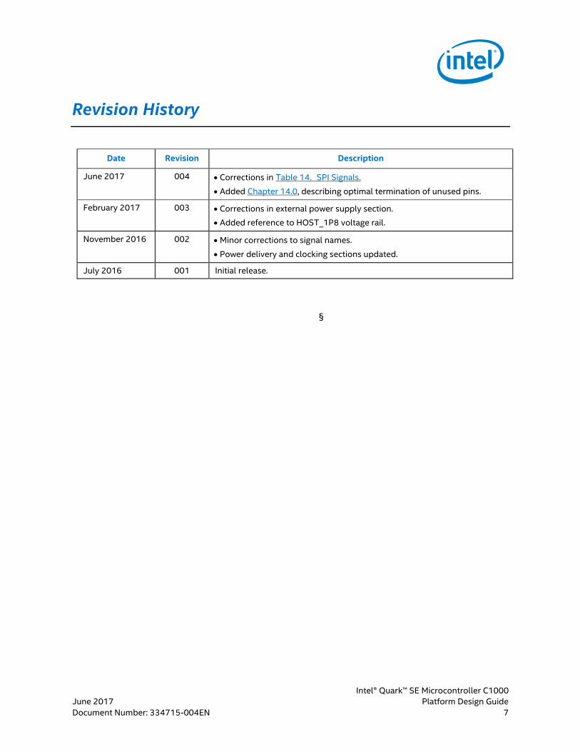
Revision History
Date Revision Description
June 2017 004 Corrections in Table 14. SPI Signals.
Added Chapter 14.0, describing optimal termination of unused pins.
February 2017 003 Corrections in external power supply section.
Added reference to HOST_1P8 voltage rail.
November 2016 002 Minor corrections to signal names.
Power delivery and clocking sections updated.
July 2016 001 Initial release.
§
Introduction
Intel® Quark™ SE Microcontroller C1000
Platform Design Guide June 2017
8 Document Number: 334715-004EN
1.0 Introduction
1.1 Overview
This design guide provides motherboard implementation recommendations for the
Intel® Quark™ SE microcontroller C1000 platform, based on the Intel® Quark™ SE
microcontroller processor. This document includes design guidelines for Intel®
Quark™ SE microcontroller platforms and the hardware integration aspects that
must be considered when designing a platform.
This design guide has been developed to ensure maximum flexibility for board
designers while reducing the risk of board-related issues. Design recommendations
are based on Intel's simulations and lab experience and are strongly recommended,
if not necessary, to meet the timing and signal quality specifications. Design
recommendations are based on the reference platforms designed by Intel. They
should be used as an example but may not be applicable to particular designs.
Note: The guidelines recommended in this document are based on experience,
simulation, and preliminary validation work done at Intel while developing the Intel®
Quark™ SE microcontroller C1000 processor-based platform. This work is ongoing,
and these recommendations are subject to change.
Caution: If the guidelines listed in this document are not followed, it is very important that the designers perform thorough signal integrity and timing simulations. Even when following these guidelines, Intel recommends the critical signals to be simulated to ensure proper signal integrity and flight time. Any deviation from the guidelines should be simulated.
Metric units are used in some sections in addition to the standard use of U.S.
customary system of units (USCS). If there is a discrepancy between the metric and
USCS units, assume the USCS unit is most accurate. The conversion factor used is
1 inch (1000 mils) = 25.4 mm.
1.2 Audience and Purpose
The Intel® Quark™ SE microcontroller C1000 is a highly integrated, ultra-low-power
part designed to enable innovative solutions with long battery life for
fitness/health/wellness monitors, smart watches, and so on.
This document is intended to aid platform hardware designers in system
implementation and reference design reuse through the following:
Documenting the hardware implementation of specific form factor solutions
based on the Intel® Quark™ SE microcontroller C1000 platform
Providing details such as block diagrams, which illustrate connectivity, system
level considerations, options, and design guidelines
Introduction
Intel® Quark™ SE Microcontroller C1000
June 2017 Platform Design Guide
Document Number: 334715-004EN 9
Describing the theory of operation or principles considered in deriving a design
guideline
1.3 Terminology
Table 1. Terminology
Term Description
ADC Analog-to-Digital Converter
CRB Customer Reference Board
GPIO General Purpose Input/Output
I2C Inter-Integrated Circuit
I2S Inter-IC Sound
JTAG Joint Test Action Group
OSC Oscillator
PWM Pulse Width Modulation
RTC Real-Time Clock
SIO Serial I/O
SoC System on Chip
SPI Serial Peripheral Interface
UART Universal Asynchronous Receiver Transmitter
VR Voltage Regulator
XTAL Crystal
1.4 Reference Documents
Table 2. Reference Documents
Document Document No./Location
Intel® Quark™ SE Microcontroller C1000 Datasheet 334712
Intel® Quark™ SE Microcontroller C1000 Power Sequencing Considerations Application Note
335277
§
System Assumptions
Intel® Quark™ SE Microcontroller C1000
Platform Design Guide June 2017
10 Document Number: 334715-004EN
2.0 System Assumptions
2.1 General Assumptions
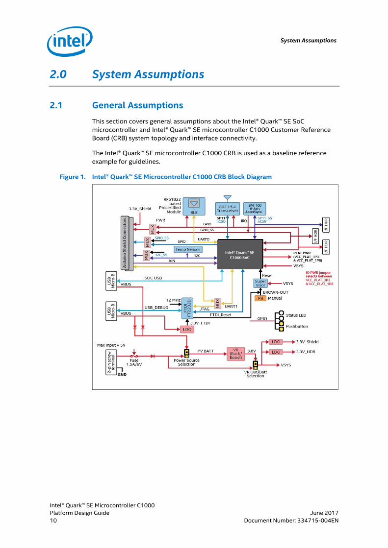
This section covers general assumptions about the Intel® Quark™ SE SoC
microcontroller and Intel® Quark™ SE microcontroller C1000 Customer Reference
Board (CRB) system topology and interface connectivity.
The Intel® Quark™ SE microcontroller C1000 CRB is used as a baseline reference
example for guidelines.
Figure 1. Intel® Quark™ SE Microcontroller C1000 CRB Block Diagram
System Assumptions
Intel® Quark™ SE Microcontroller C1000
June 2017 Platform Design Guide
Document Number: 334715-004EN 11
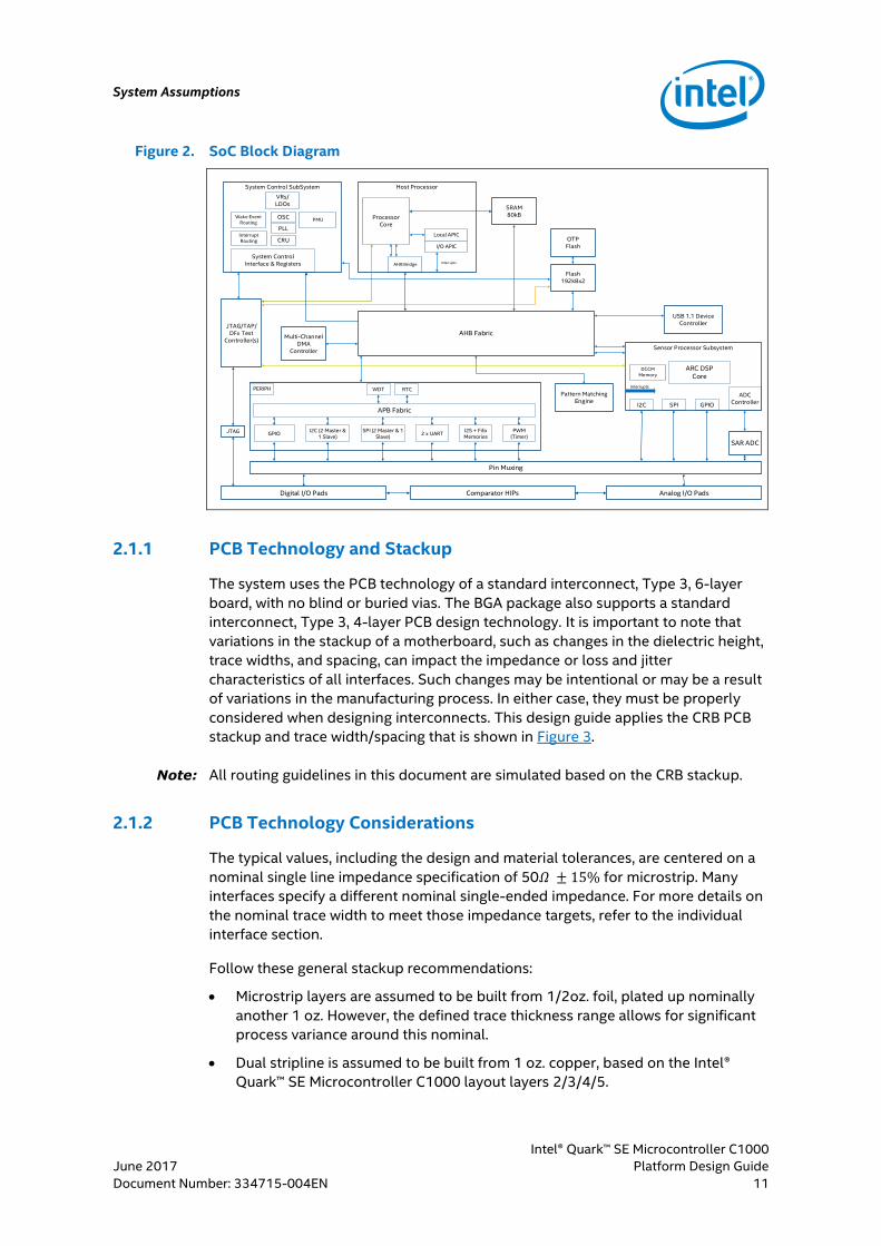
Figure 2. SoC Block Diagram
SPI GPIO
ADC ControllerI2C
AHB FabricMulti-Channel
DMAController
JTAG/TAP/DFx Test
Controller(s)
APB Fabric
WDT RTC
JTAG
Pin Muxing
Digital I/O Pads
Sensor Processor Subsystem
ARC DSPCore
SAR ADC
USB 1.1 Device Controller
Interrupts
SRAM80kB
PERIPH
Comparator HIPs Analog I/O Pads
Flash192kBx2
OTPFlash
PWM (Timer)
I2S + Fifo Memories
2 x UARTSPI (2 Master & 1
Slave)I2C (2 Master &
1 Slave)
AHB Bridge
Host Processor
ProcessorCore
Local APIC
Interrupts
I/O APIC
System ControlInterface & Registers
System Control SubSystem
VRs/LDOs
Interrupt Routing
Wake Event Routing
OSC
PLL
CRU
PMU
GPIO
DCCM Memory
Pattern Matching Engine
2.1.1 PCB Technology and Stackup
The system uses the PCB technology of a standard interconnect, Type 3, 6-layer
board, with no blind or buried vias. The BGA package also supports a standard
interconnect, Type 3, 4-layer PCB design technology. It is important to note that
variations in the stackup of a motherboard, such as changes in the dielectric height,
trace widths, and spacing, can impact the impedance or loss and jitter
characteristics of all interfaces. Such changes may be intentional or may be a result
of variations in the manufacturing process. In either case, they must be properly
considered when designing interconnects. This design guide applies the CRB PCB
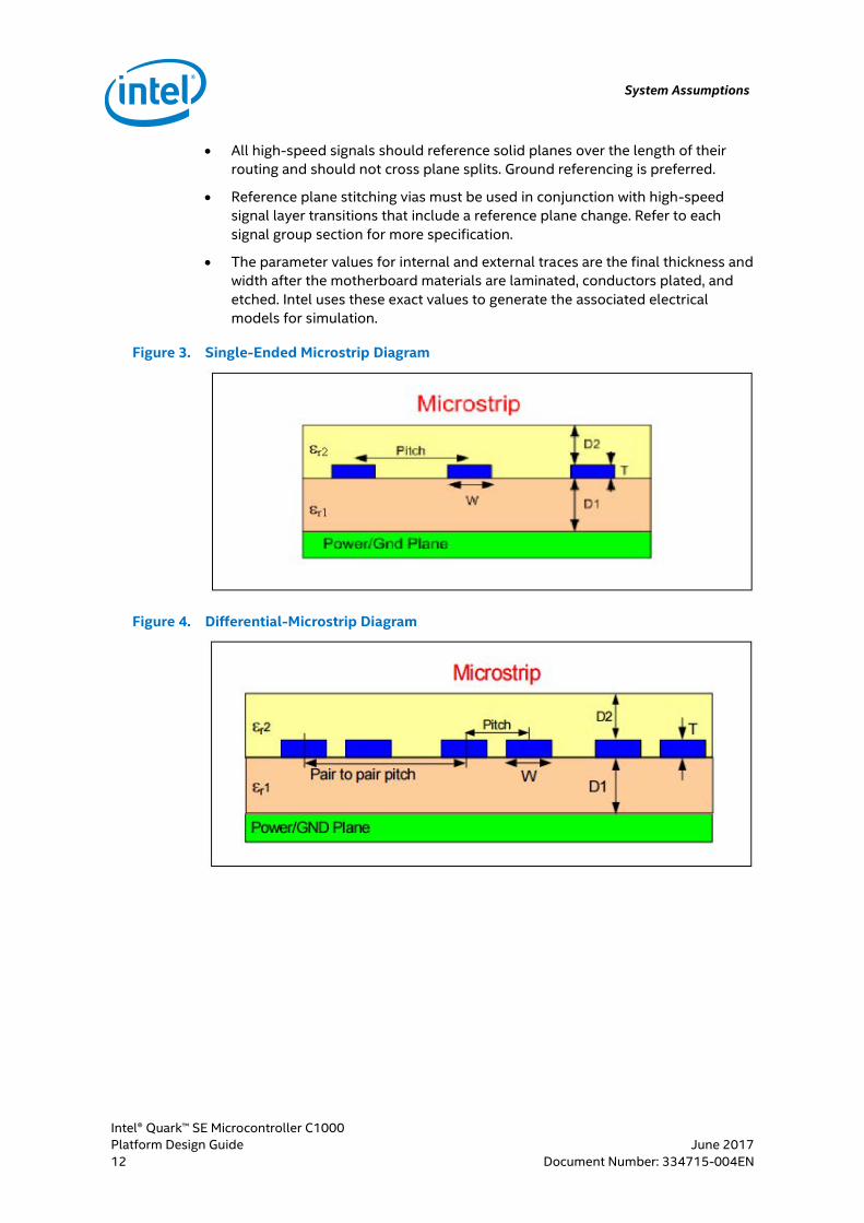
stackup and trace width/spacing that is shown in Figure 3.
Note: All routing guidelines in this document are simulated based on the CRB stackup.
2.1.2 PCB Technology Considerations
The typical values, including the design and material tolerances, are centered on a
nominal single line impedance specification of 50𝛺 ± 15% for microstrip. Many
interfaces specify a different nominal single-ended impedance. For more details on
the nominal trace width to meet those impedance targets, refer to the individual
interface section.
Follow these general stackup recommendations:
Microstrip layers are assumed to be built from 1/2oz. foil, plated up nominally
another 1 oz. However, the defined trace thickness range allows for significant
process variance around this nominal.
Dual stripline is assumed to be built from 1 oz. copper, based on the Intel®
Quark™ SE Microcontroller C1000 layout layers 2/3/4/5.
System Assumptions
Intel® Quark™ SE Microcontroller C1000
Platform Design Guide June 2017
12 Document Number: 334715-004EN
All high-speed signals should reference solid planes over the length of their
routing and should not cross plane splits. Ground referencing is preferred.
Reference plane stitching vias must be used in conjunction with high-speed
signal layer transitions that include a reference plane change. Refer to each
signal group section for more specification.
The parameter values for internal and external traces are the final thickness and
width after the motherboard materials are laminated, conductors plated, and
etched. Intel uses these exact values to generate the associated electrical
models for simulation.
Figure 3. Single-Ended Microstrip Diagram
Figure 4. Differential-Microstrip Diagram
System Assumptions
Intel® Quark™ SE Microcontroller C1000
June 2017 Platform Design Guide
Document Number: 334715-004EN 13
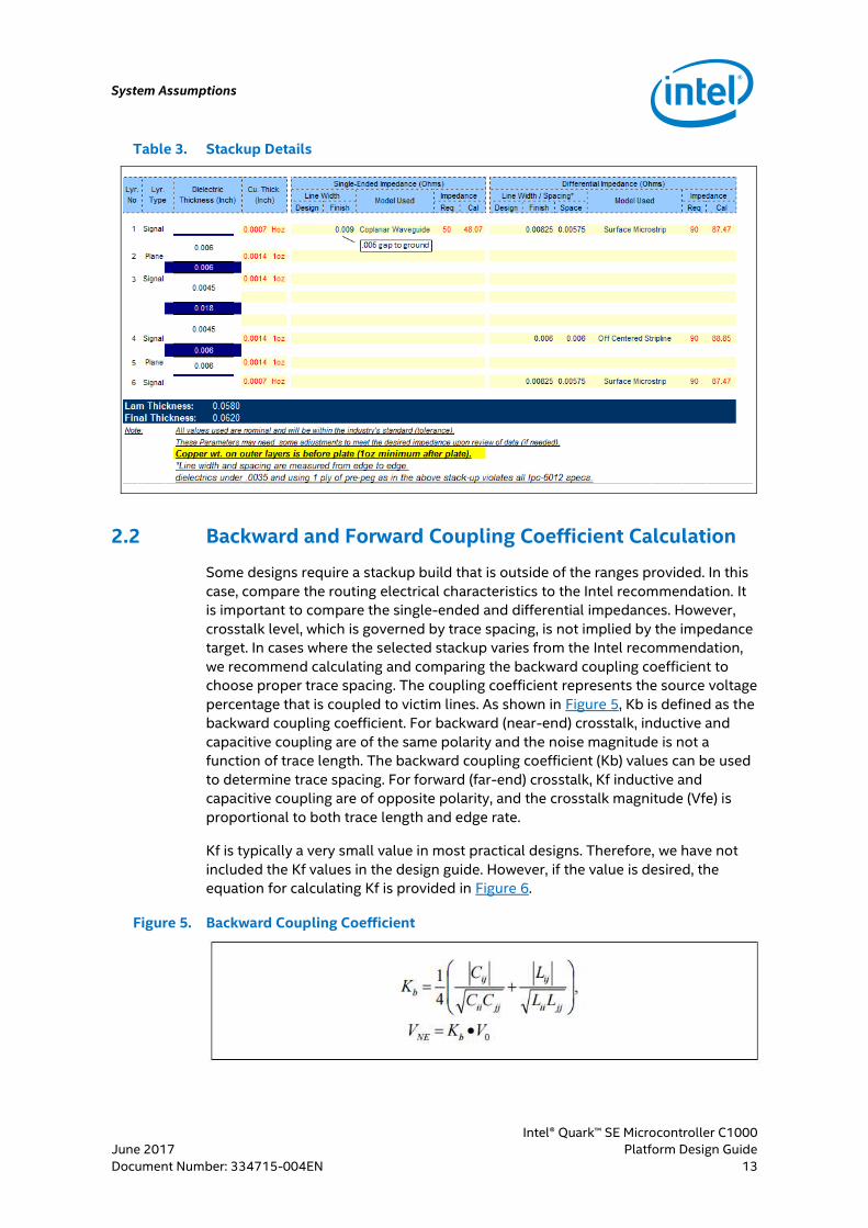
Table 3. Stackup Details
2.2 Backward and Forward Coupling Coefficient Calculation
Some designs require a stackup build that is outside of the ranges provided. In this
case, compare the routing electrical characteristics to the Intel recommendation. It
is important to compare the single-ended and differential impedances. However,
crosstalk level, which is governed by trace spacing, is not implied by the impedance
target. In cases where the selected stackup varies from the Intel recommendation,
we recommend calculating and comparing the backward coupling coefficient to
choose proper trace spacing. The coupling coefficient represents the source voltage
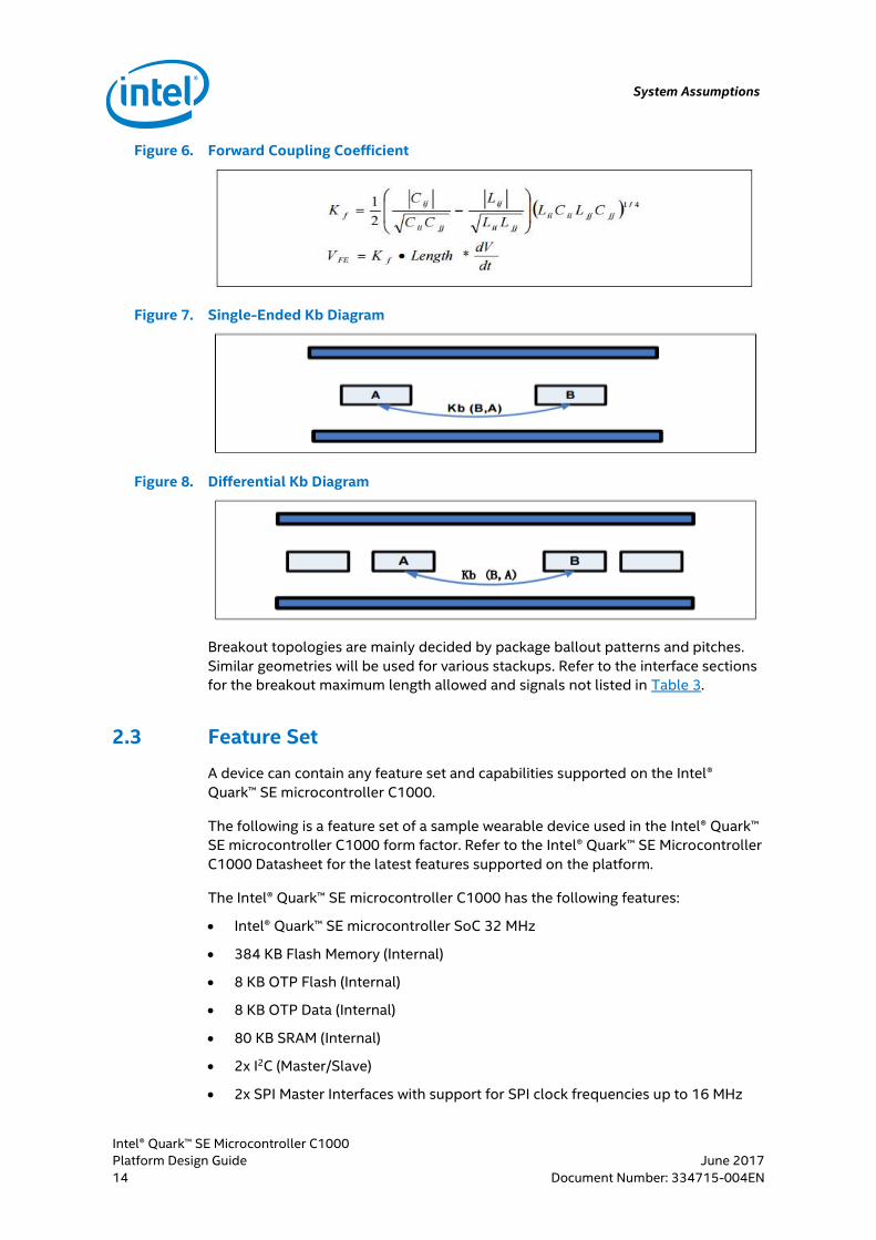
percentage that is coupled to victim lines. As shown in Figure 5, Kb is defined as the
backward coupling coefficient. For backward (near-end) crosstalk, inductive and
capacitive coupling are of the same polarity and the noise magnitude is not a
function of trace length. The backward coupling coefficient (Kb) values can be used
to determine trace spacing. For forward (far-end) crosstalk, Kf inductive and
capacitive coupling are of opposite polarity, and the crosstalk magnitude (Vfe) is
proportional to both trace length and edge rate.
Kf is typically a very small value in most practical designs. Therefore, we have not
included the Kf values in the design guide. However, if the value is desired, the
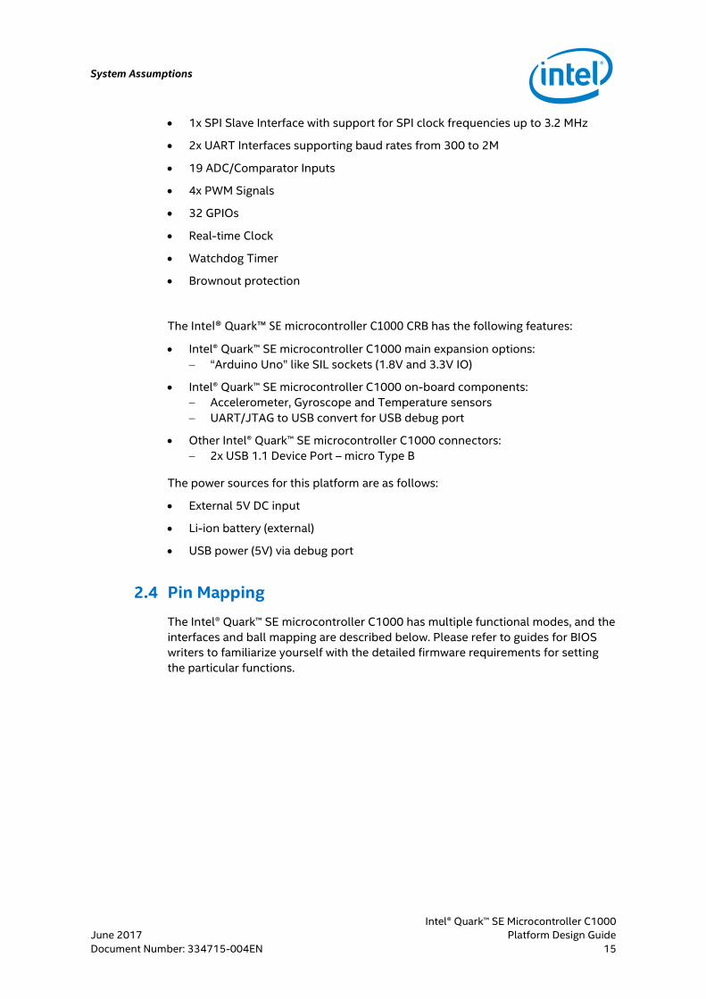
equation for calculating Kf is provided in Figure 6.
Figure 5. Backward Coupling Coefficient
System Assumptions
Intel® Quark™ SE Microcontroller C1000
Platform Design Guide June 2017
14 Document Number: 334715-004EN
Figure 6. Forward Coupling Coefficient
Figure 7. Single-Ended Kb Diagram
Figure 8. Differential Kb Diagram
Breakout topologies are mainly decided by package ballout patterns and pitches.
Similar geometries will be used for various stackups. Refer to the interface sections
for the breakout maximum length allowed and signals not listed in Table 3.
2.3 Feature Set
A device can contain any feature set and capabilities supported on the Intel®
Quark™ SE microcontroller C1000.
The following is a feature set of a sample wearable device used in the Intel® Quark™
SE microcontroller C1000 form factor. Refer to the Intel® Quark™ SE Microcontroller
C1000 Datasheet for the latest features supported on the platform.
The Intel® Quark™ SE microcontroller C1000 has the following features:
Intel® Quark™ SE microcontroller SoC 32 MHz
384 KB Flash Memory (Internal)
8 KB OTP Flash (Internal)
8 KB OTP Data (Internal)
80 KB SRAM (Internal)
2x I2C (Master/Slave)
2x SPI Master Interfaces with support for SPI clock frequencies up to 16 MHz
System Assumptions
Intel® Quark™ SE Microcontroller C1000
June 2017 Platform Design Guide
Document Number: 334715-004EN 15
1x SPI Slave Interface with support for SPI clock frequencies up to 3.2 MHz
2x UART Interfaces supporting baud rates from 300 to 2M
19 ADC/Comparator Inputs
4x PWM Signals
32 GPIOs
Real-time Clock
Watchdog Timer
Brownout protection
The Intel® Quark™ SE microcontroller C1000 CRB has the following features:
Intel® Quark™ SE microcontroller C1000 main expansion options:
“Arduino Uno” like SIL sockets (1.8V and 3.3V IO)
Intel® Quark™ SE microcontroller C1000 on-board components:
Accelerometer, Gyroscope and Temperature sensors
UART/JTAG to USB convert for USB debug port
Other Intel® Quark™ SE microcontroller C1000 connectors:
2x USB 1.1 Device Port – micro Type B
The power sources for this platform are as follows:
External 5V DC input
Li-ion battery (external)
USB power (5V) via debug port
2.4 Pin Mapping
The Intel® Quark™ SE microcontroller C1000 has multiple functional modes, and the
interfaces and ball mapping are described below. Please refer to guides for BIOS
writers to familiarize yourself with the detailed firmware requirements for setting
the particular functions.
System Assumptions
Intel® Quark™ SE Microcontroller C1000
Platform Design Guide June 2017
16 Document Number: 334715-004EN
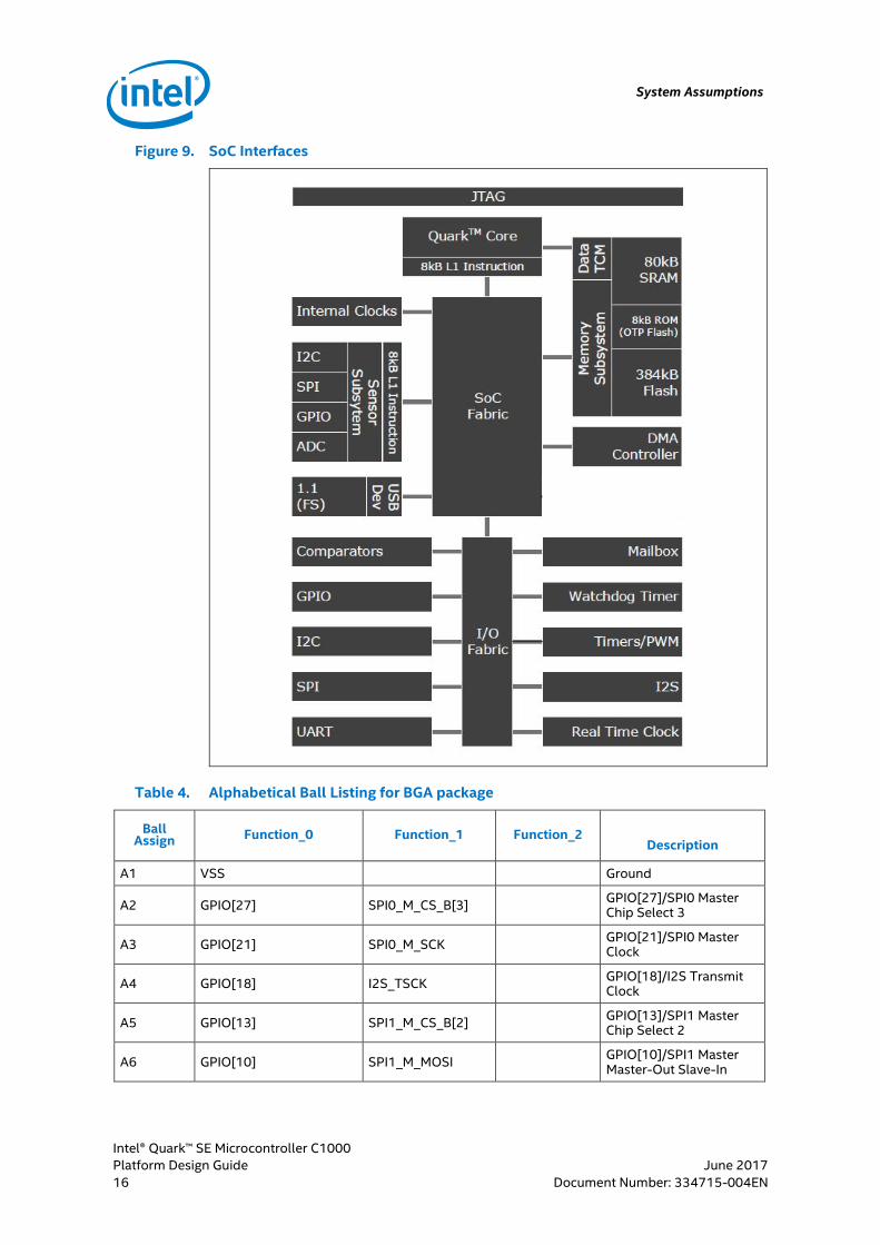
Figure 9. SoC Interfaces
Table 4. Alphabetical Ball Listing for BGA package
Ball Assign Function_0 Function_1 Function_2
Description
A1 VSS Ground
A2 GPIO[27] SPI0_M_CS_B[3] GPIO[27]/SPI0 Master Chip Select 3
A3 GPIO[21] SPI0_M_SCK GPIO[21]/SPI0 Master Clock
A4 GPIO[18] I2S_TSCK GPIO[18]/I2S Transmit Clock
A5 GPIO[13] SPI1_M_CS_B[2] GPIO[13]/SPI1 Master Chip Select 2
A6 GPIO[10] SPI1_M_MOSI GPIO[10]/SPI1 Master Master-Out Slave-In
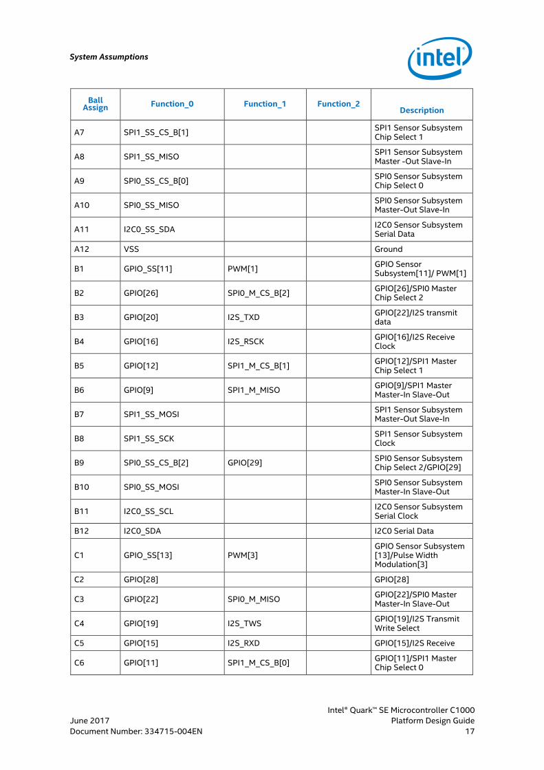
System Assumptions
Intel® Quark™ SE Microcontroller C1000
June 2017 Platform Design Guide
Document Number: 334715-004EN 17
Ball Assign Function_0 Function_1 Function_2
Description
A7 SPI1_SS_CS_B[1] SPI1 Sensor Subsystem Chip Select 1
A8 SPI1_SS_MISO SPI1 Sensor Subsystem Master -Out Slave-In
A9 SPI0_SS_CS_B[0] SPI0 Sensor Subsystem Chip Select 0
A10 SPI0_SS_MISO SPI0 Sensor Subsystem Master-Out Slave-In
A11 I2C0_SS_SDA I2C0 Sensor Subsystem Serial Data
A12 VSS Ground
B1 GPIO_SS[11] PWM[1] GPIO Sensor Subsystem[11]/ PWM[1]
B2 GPIO[26] SPI0_M_CS_B[2] GPIO[26]/SPI0 Master Chip Select 2
B3 GPIO[20] I2S_TXD GPIO[22]/I2S transmit data
B4 GPIO[16] I2S_RSCK GPIO[16]/I2S Receive Clock
B5 GPIO[12] SPI1_M_CS_B[1] GPIO[12]/SPI1 Master Chip Select 1
B6 GPIO[9] SPI1_M_MISO GPIO[9]/SPI1 Master Master-In Slave-Out
B7 SPI1_SS_MOSI SPI1 Sensor Subsystem Master-Out Slave-In
B8 SPI1_SS_SCK SPI1 Sensor Subsystem Clock
B9 SPI0_SS_CS_B[2] GPIO[29] SPI0 Sensor Subsystem Chip Select 2/GPIO[29]
B10 SPI0_SS_MOSI SPI0 Sensor Subsystem Master-In Slave-Out
B11 I2C0_SS_SCL I2C0 Sensor Subsystem Serial Clock
B12 I2C0_SDA I2C0 Serial Data
C1 GPIO_SS[13] PWM[3] GPIO Sensor Subsystem [13]/Pulse Width Modulation[3]
C2 GPIO[28] GPIO[28]
C3 GPIO[22] SPI0_M_MISO GPIO[22]/SPI0 Master Master-In Slave-Out
C4 GPIO[19] I2S_TWS GPIO[19]/I2S Transmit Write Select
C5 GPIO[15] I2S_RXD GPIO[15]/I2S Receive
C6 GPIO[11] SPI1_M_CS_B[0] GPIO[11]/SPI1 Master Chip Select 0
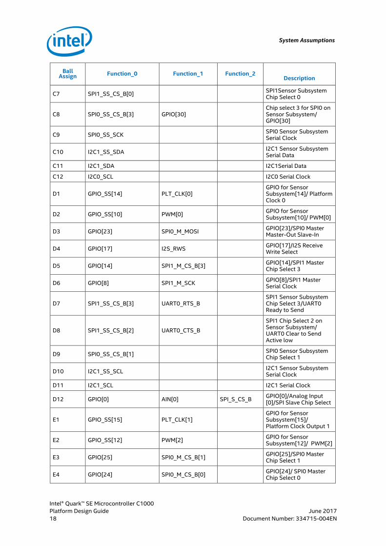
System Assumptions
Intel® Quark™ SE Microcontroller C1000
Platform Design Guide June 2017
18 Document Number: 334715-004EN
Ball Assign Function_0 Function_1 Function_2
Description
C7 SPI1_SS_CS_B[0] SPI1Sensor Subsystem Chip Select 0
C8 SPI0_SS_CS_B[3] GPIO[30] Chip select 3 for SPI0 on Sensor Subsystem/ GPIO[30]
C9 SPI0_SS_SCK SPI0 Sensor Subsystem Serial Clock
C10 I2C1_SS_SDA I2C1 Sensor Subsystem Serial Data
C11 I2C1_SDA I2C1Serial Data
C12 I2C0_SCL I2C0 Serial Clock
D1 GPIO_SS[14] PLT_CLK[0] GPIO for Sensor Subsystem[14]/ Platform Clock 0
D2 GPIO_SS[10] PWM[0] GPIO for Sensor Subsystem[10]/ PWM[0]
D3 GPIO[23] SPI0_M_MOSI GPIO[23]/SPI0 Master Master-Out Slave-In
D4 GPIO[17] I2S_RWS GPIO[17]/I2S Receive Write Select
D5 GPIO[14] SPI1_M_CS_B[3] GPIO[14]/SPI1 Master Chip Select 3
D6 GPIO[8] SPI1_M_SCK GPIO[8]/SPI1 Master Serial Clock
D7 SPI1_SS_CS_B[3] UART0_RTS_B SPI1 Sensor Subsystem Chip Select 3/UART0 Ready to Send
D8 SPI1_SS_CS_B[2] UART0_CTS_B
SPI1 Chip Select 2 on Sensor Subsystem/ UART0 Clear to Send Active low
D9 SPI0_SS_CS_B[1] SPI0 Sensor Subsystem Chip Select 1
D10 I2C1_SS_SCL I2C1 Sensor Subsystem Serial Clock
D11 I2C1_SCL I2C1 Serial Clock
D12 GPIO[0] AIN[0] SPI_S_CS_B GPIO[0]/Analog Input [0]/SPI Slave Chip Select
E1 GPIO_SS[15] PLT_CLK[1] GPIO for Sensor Subsystem[15]/ Platform Clock Output 1
E2 GPIO_SS[12] PWM[2] GPIO for Sensor Subsystem[12]/ PWM[2]
E3 GPIO[25] SPI0_M_CS_B[1] GPIO[25]/SPI0 Master Chip Select 1
E4 GPIO[24] SPI0_M_CS_B[0] GPIO[24]/ SPI0 Master Chip Select 0
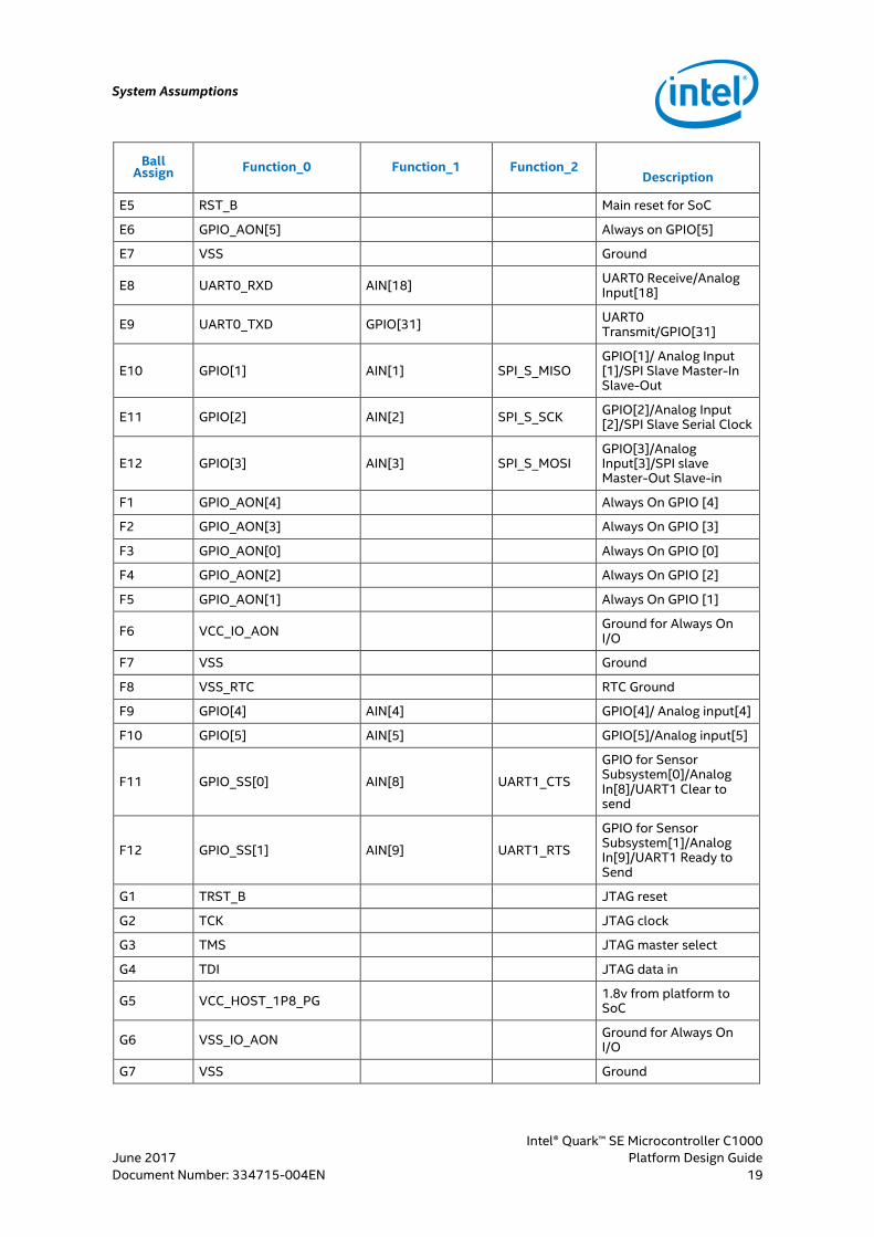
System Assumptions
Intel® Quark™ SE Microcontroller C1000
June 2017 Platform Design Guide
Document Number: 334715-004EN 19
Ball Assign Function_0 Function_1 Function_2
Description
E5 RST_B Main reset for SoC
E6 GPIO_AON[5] Always on GPIO[5]
E7 VSS Ground
E8 UART0_RXD AIN[18] UART0 Receive/Analog Input[18]
E9 UART0_TXD GPIO[31] UART0 Transmit/GPIO[31]
E10 GPIO[1] AIN[1] SPI_S_MISO GPIO[1]/ Analog Input [1]/SPI Slave Master-In Slave-Out
E11 GPIO[2] AIN[2] SPI_S_SCK GPIO[2]/Analog Input [2]/SPI Slave Serial Clock
E12 GPIO[3] AIN[3] SPI_S_MOSI GPIO[3]/Analog Input[3]/SPI slave Master-Out Slave-in
F1 GPIO_AON[4] Always On GPIO [4]
F2 GPIO_AON[3] Always On GPIO [3]
F3 GPIO_AON[0] Always On GPIO [0]
F4 GPIO_AON[2] Always On GPIO [2]
F5 GPIO_AON[1] Always On GPIO [1]
F6 VCC_IO_AON Ground for Always On I/O
F7 VSS Ground
F8 VSS_RTC RTC Ground
F9 GPIO[4] AIN[4] GPIO[4]/ Analog input[4]
F10 GPIO[5] AIN[5] GPIO[5]/Analog input[5]
F11 GPIO_SS[0] AIN[8] UART1_CTS
GPIO for Sensor Subsystem[0]/Analog In[8]/UART1 Clear to send
F12 GPIO_SS[1] AIN[9] UART1_RTS
GPIO for Sensor Subsystem[1]/Analog In[9]/UART1 Ready to Send
G1 TRST_B JTAG reset
G2 TCK JTAG clock
G3 TMS JTAG master select
G4 TDI JTAG data in
G5 VCC_HOST_1P8_PG 1.8v from platform to SoC
G6 VSS_IO_AON Ground for Always On I/O
G7 VSS Ground
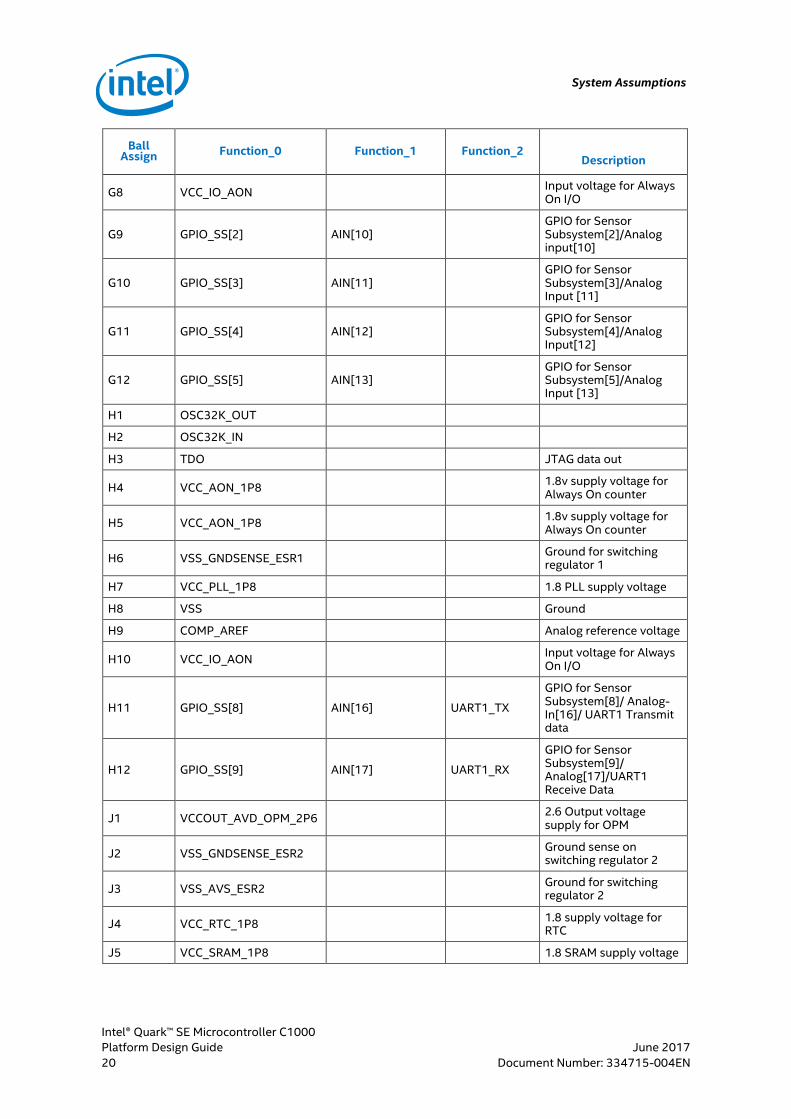
System Assumptions
Intel® Quark™ SE Microcontroller C1000
Platform Design Guide June 2017
20 Document Number: 334715-004EN
Ball Assign Function_0 Function_1 Function_2
Description
G8 VCC_IO_AON Input voltage for Always On I/O
G9 GPIO_SS[2] AIN[10] GPIO for Sensor Subsystem[2]/Analog input[10]
G10 GPIO_SS[3] AIN[11] GPIO for Sensor Subsystem[3]/Analog Input [11]
G11 GPIO_SS[4] AIN[12] GPIO for Sensor Subsystem[4]/Analog Input[12]
G12 GPIO_SS[5] AIN[13] GPIO for Sensor Subsystem[5]/Analog Input [13]
H1 OSC32K_OUT
H2 OSC32K_IN
H3 TDO JTAG data out
H4 VCC_AON_1P8 1.8v supply voltage for Always On counter
H5 VCC_AON_1P8 1.8v supply voltage for Always On counter
H6 VSS_GNDSENSE_ESR1 Ground for switching regulator 1
H7 VCC_PLL_1P8 1.8 PLL supply voltage
H8 VSS Ground
H9 COMP_AREF Analog reference voltage
H10 VCC_IO_AON Input voltage for Always On I/O
H11 GPIO_SS[8] AIN[16] UART1_TX
GPIO for Sensor Subsystem[8]/ Analog-In[16]/ UART1 Transmit data
H12 GPIO_SS[9] AIN[17] UART1_RX
GPIO for Sensor Subsystem[9]/ Analog[17]/UART1 Receive Data
J1 VCCOUT_AVD_OPM_2P6 2.6 Output voltage supply for OPM
J2 VSS_GNDSENSE_ESR2 Ground sense on switching regulator 2
J3 VSS_AVS_ESR2 Ground for switching regulator 2
J4 VCC_RTC_1P8 1.8 supply voltage for RTC
J5 VCC_SRAM_1P8 1.8 SRAM supply voltage
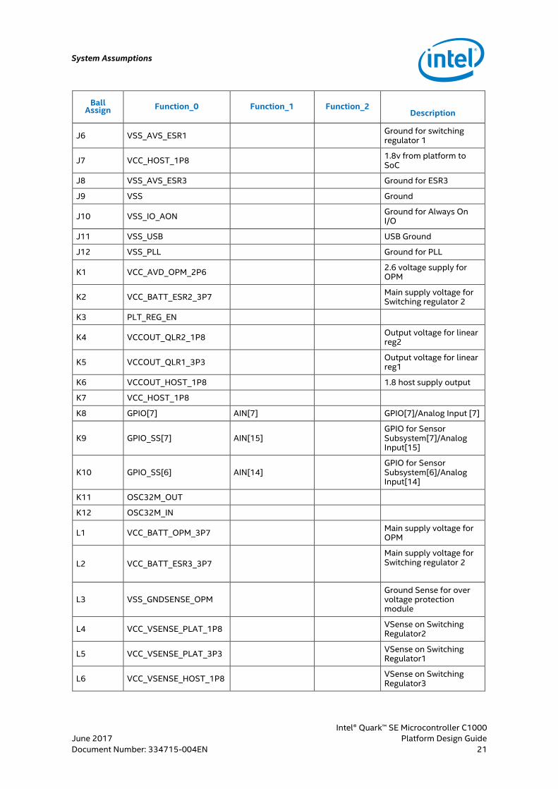
System Assumptions
Intel® Quark™ SE Microcontroller C1000
June 2017 Platform Design Guide
Document Number: 334715-004EN 21
Ball Assign Function_0 Function_1 Function_2
Description
J6 VSS_AVS_ESR1 Ground for switching regulator 1
J7 VCC_HOST_1P8 1.8v from platform to SoC
J8 VSS_AVS_ESR3 Ground for ESR3
J9 VSS Ground
J10 VSS_IO_AON Ground for Always On I/O
J11 VSS_USB USB Ground
J12 VSS_PLL Ground for PLL
K1 VCC_AVD_OPM_2P6 2.6 voltage supply for OPM
K2 VCC_BATT_ESR2_3P7 Main supply voltage for Switching regulator 2
K3 PLT_REG_EN
K4 VCCOUT_QLR2_1P8 Output voltage for linear reg2
K5 VCCOUT_QLR1_3P3 Output voltage for linear reg1
K6 VCCOUT_HOST_1P8 1.8 host supply output
K7 VCC_HOST_1P8
K8 GPIO[7] AIN[7] GPIO[7]/Analog Input [7]
K9 GPIO_SS[7] AIN[15] GPIO for Sensor Subsystem[7]/Analog Input[15]
K10 GPIO_SS[6] AIN[14] GPIO for Sensor Subsystem[6]/Analog Input[14]
K11 OSC32M_OUT
K12 OSC32M_IN
L1 VCC_BATT_OPM_3P7 Main supply voltage for OPM
L2 VCC_BATT_ESR3_3P7
Main supply voltage for Switching regulator 2
L3 VSS_GNDSENSE_OPM Ground Sense for over voltage protection module
L4 VCC_VSENSE_PLAT_1P8 VSense on Switching Regulator2
L5 VCC_VSENSE_PLAT_3P3 VSense on Switching Regulator1
L6 VCC_VSENSE_HOST_1P8 VSense on Switching Regulator3
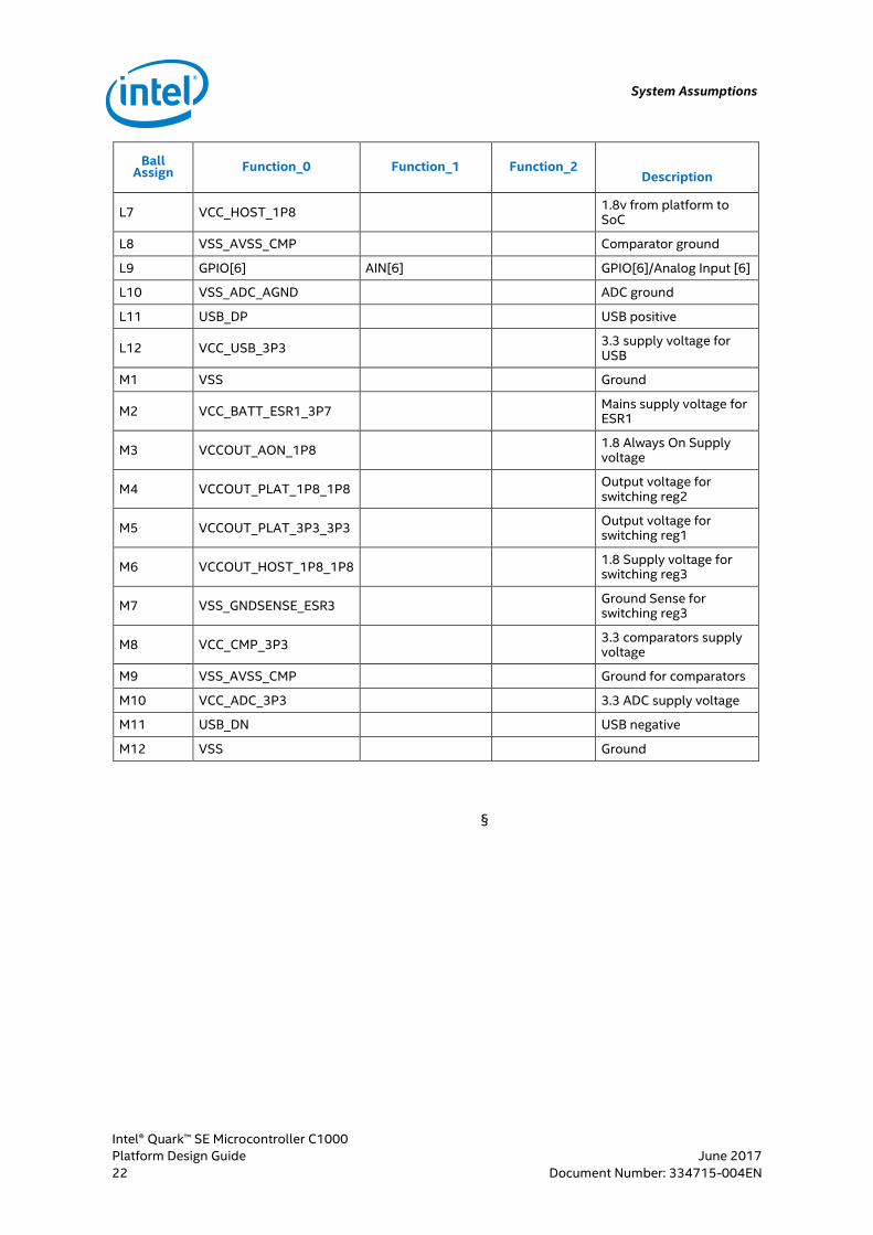
System Assumptions
Intel® Quark™ SE Microcontroller C1000
Platform Design Guide June 2017
22 Document Number: 334715-004EN
Ball Assign Function_0 Function_1 Function_2
Description
L7 VCC_HOST_1P8 1.8v from platform to SoC
L8 VSS_AVSS_CMP Comparator ground
L9 GPIO[6] AIN[6] GPIO[6]/Analog Input [6]
L10 VSS_ADC_AGND ADC ground
L11 USB_DP USB positive
L12 VCC_USB_3P3 3.3 supply voltage for USB
M1 VSS Ground
M2 VCC_BATT_ESR1_3P7 Mains supply voltage for ESR1
M3 VCCOUT_AON_1P8 1.8 Always On Supply voltage
M4 VCCOUT_PLAT_1P8_1P8 Output voltage for switching reg2
M5 VCCOUT_PLAT_3P3_3P3 Output voltage for switching reg1
M6 VCCOUT_HOST_1P8_1P8 1.8 Supply voltage for switching reg3
M7 VSS_GNDSENSE_ESR3 Ground Sense for switching reg3
M8 VCC_CMP_3P3 3.3 comparators supply voltage
M9 VSS_AVSS_CMP Ground for comparators
M10 VCC_ADC_3P3 3.3 ADC supply voltage
M11 USB_DN USB negative
M12 VSS Ground
§

Subsystem Details
Intel® Quark™ SE Microcontroller C1000
June 2017 Platform Design Guide
Document Number: 334715-004EN 23
3.0 Subsystem Details
This chapter provides design guidelines for the SoC associated interfaces. All
routing guidelines (W/S, isolation, length requirement) are based on CRB 6-layer
PCB technology. If a different PCB stackup is implemented, the electrical guidelines
(impedance, Kb, Insertion Loss) provided in this document must be followed to
ensure that the layout can meet simulation recommendations.
3.1 Design Recommendations
The Intel® Quark™ SE microcontroller C1000 is an ultra-low-power Intel®
architecture SoC that integrates an Intel® Quark™ SE microcontroller processor core,
memory subsystem with on-die volatile and non-volatile storage, and I/O interfaces
into a single system-on-chip solution.
This section presents design recommendations for the subsystems that make up
the Intel® Quark™ SE microcontroller C1000 platform. It includes overview
information, component selection studies, suggested routing guidelines, and
additional filter and signal information for the Intel® Quark™ SE microcontroller
C1000 platform.
The design recommendations are developed to ensure maximum flexibility for
board designers while reducing the risk of board-related issues.
Note: These design recommendations should be carefully followed and any deviations
should be verified through simulations. The component selection
recommendations describe the components that are being considered for the Intel®
Quark™ SE microcontroller C1000. If and when updated boards become available,
this will be noted in these sections.
The following subsystems are covered in this section:
I2C
PWM
UART
SPI
RTC
GPIO
JTAG
ADC
USB
Subsystem Details
Intel® Quark™ SE Microcontroller C1000
Platform Design Guide June 2017
24 Document Number: 334715-004EN
3.2 General Design Guideline Assumptions
The following assumptions pertain to all the subsystems discussed in this chapter:
Package length compensation is needed. The length values are tested and
measured as package-pin-to-package-pin.
The breakout and breaking minimum spacing ratio is 1:1 for all interfaces.
The trace width/intra-spacing for differential pairs and trace width for single-
ended signals depend on the impedance.
For analog signals, it is important to keep the analog ground return path clean
of digital noise to maintain a high signal-to-noise ratio.
Note: If a specific interface design guide is not available, follow the general guidelines in
this section.
Note: All routing guidelines in this document are simulated based on the CRB stackup.
Note: For technical specifications (such as speeds, supported resolutions, and data rates),
please refer to the Intel® Quark™ SE Microcontroller C1000 Datasheet.
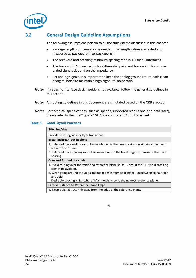
Table 5. Good Layout Practices
Stitching Vias
Provide stitching vias for layer transitions.
Break-in/Break-out Regions
1. If desired trace width cannot be maintained in the break regions, maintain a minimum
trace width of 3.5 mil.
2. If desired trace spacing cannot be maintained in the break regions, maximize the trace
spacing.
Over and Around the voids
1. Avoid routing over the voids and reference plane splits. Consult the SIE if split crossing
cannot be avoided.
2. When going around the voids, maintain a minimum spacing of 1xh between signal trace
and void.
Desirable spacing is 3xh where "h" is the distance to the nearest reference plane.
Lateral Distance to Reference Plane Edge
1. Keep a signal trace 4xh away from the edge of the reference plane.
§
I2C Interface
Intel® Quark™ SE Microcontroller C1000
June 2017 Platform Design Guide
Document Number: 334715-004EN 25
4.0 I2C Interface
I2C is a two-wire serial bus for inter-IC communication. One wire is for data, and the
other wire is for clock. The Intel® Quark™ SE microcontroller C1000 has two I2C
controllers, each with its own independent two-wire bus.
4.1 I2C Interfaces Signals
Signals for the I2C interfaces are illustrated in the table below.
Table 6. I2C Interface Signals
Signal Name Direction/ Type Description
I2C_M_x_CLK I/O I2C Serial Clock
I2C_M_x_DATA I/O I2C Serial Data
The following is a list of the I2C features:
Two I2C interfaces
Support for both master and slave operation
Operational speeds:
Standard mode (0 to 100Kbps)
Fast mode (≤ 400Kbps)
Fast mode plus (≤ 1Mbps)
7-bit or 10-bit addressing
Support for clock stretching by slave devices
Multi-master arbitration
Spike suppression
Hardware handshake interface to support DMA capability
Interrupt control
FIFO support with 16B deep RX and TX FIFOs
4.2 Interface Routing Guidelines
I2C clock and data signals require pull-up resistors. The pull-up size is dependent
on the bus capacitive load (this includes all device leakage currents).
I2C Interface
Intel® Quark™ SE Microcontroller C1000
Platform Design Guide June 2017
26 Document Number: 334715-004EN
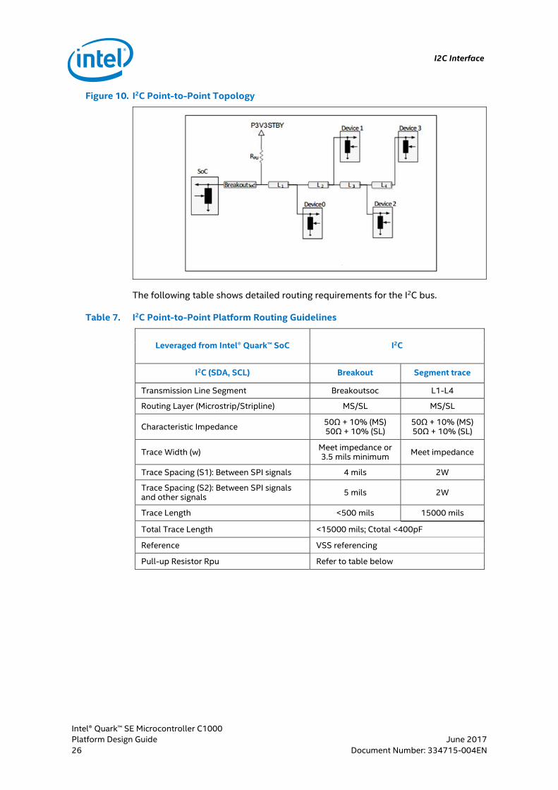
Figure 10. I2C Point-to-Point Topology
The following table shows detailed routing requirements for the I2C bus.
Table 7. I2C Point-to-Point Platform Routing Guidelines
Leveraged from Intel® Quark™ SoC I2C
I2C (SDA, SCL) Breakout Segment trace
Transmission Line Segment Breakoutsoc L1-L4
Routing Layer (Microstrip/Stripline) MS/SL MS/SL
Characteristic Impedance 50Ω + 10% (MS) 50Ω + 10% (SL)
50Ω + 10% (MS) 50Ω + 10% (SL)
Trace Width (w) Meet impedance or 3.5 mils minimum
Meet impedance
Trace Spacing (S1): Between SPI signals 4 mils 2W
Trace Spacing (S2): Between SPI signals and other signals
5 mils 2W
Trace Length <500 mils 15000 mils
Total Trace Length <15000 mils; Ctotal <400pF
Reference VSS referencing
Pull-up Resistor Rpu Refer to table below
I2C Interface
Intel® Quark™ SE Microcontroller C1000
June 2017 Platform Design Guide
Document Number: 334715-004EN 27
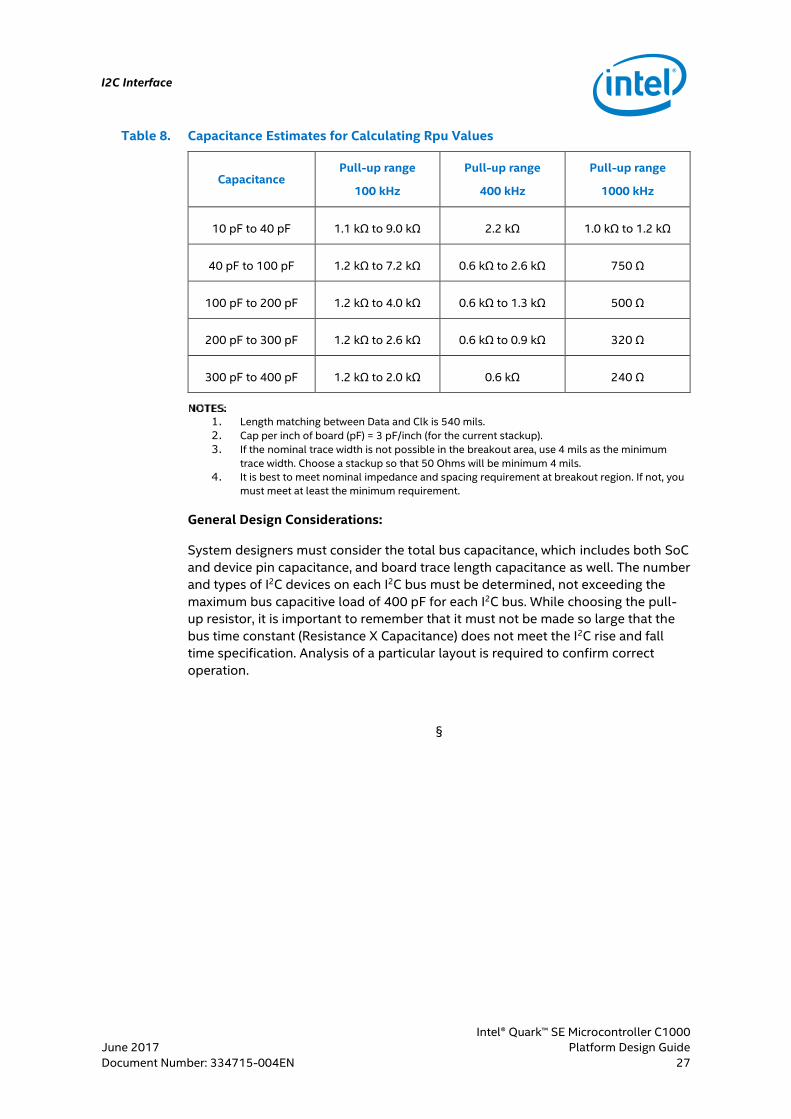
Table 8. Capacitance Estimates for Calculating Rpu Values
Capacitance Pull-up range
100 kHz
Pull-up range
400 kHz
Pull-up range
1000 kHz
10 pF to 40 pF 1.1 kΩ to 9.0 kΩ 2.2 kΩ 1.0 kΩ to 1.2 kΩ
40 pF to 100 pF 1.2 kΩ to 7.2 kΩ 0.6 kΩ to 2.6 kΩ 750 Ω
100 pF to 200 pF 1.2 kΩ to 4.0 kΩ 0.6 kΩ to 1.3 kΩ 500 Ω
200 pF to 300 pF 1.2 kΩ to 2.6 kΩ 0.6 kΩ to 0.9 kΩ 320 Ω
300 pF to 400 pF 1.2 kΩ to 2.0 kΩ 0.6 kΩ 240 Ω
1. Length matching between Data and Clk is 540 mils.
2. Cap per inch of board (pF) = 3 pF/inch (for the current stackup).
3. If the nominal trace width is not possible in the breakout area, use 4 mils as the minimum
trace width. Choose a stackup so that 50 Ohms will be minimum 4 mils.
4. It is best to meet nominal impedance and spacing requirement at breakout region. If not, you
must meet at least the minimum requirement.
General Design Considerations:
System designers must consider the total bus capacitance, which includes both SoC
and device pin capacitance, and board trace length capacitance as well. The number
and types of I2C devices on each I2C bus must be determined, not exceeding the
maximum bus capacitive load of 400 pF for each I2C bus. While choosing the pull-
up resistor, it is important to remember that it must not be made so large that the
bus time constant (Resistance X Capacitance) does not meet the I2C rise and fall
time specification. Analysis of a particular layout is required to confirm correct
operation.
§
Pulse Width Modulation (PWM)
Intel® Quark™ SE Microcontroller C1000
Platform Design Guide June 2017
28 Document Number: 334715-004EN
5.0 Pulse Width Modulation (PWM)
The Pulse Width Modulation (PWM) block allows individual control of the frequency
and duty cycle of four output signals. The PWM block also supports use as a Timer
block for the purposes of generating periodic interrupts. A possible usage model
includes connecting PWM to drive a haptic driver. The four PWM pins are also
multiplexed and can be used as a GPIO. Four 32-bit timers running at system clock
can be configured to generate four PWM outputs.
Table 9. PWM Interface Signals
Signal Name Direction/ Type Description
PWM[0] Output PWM output 0
PWM[1] Output PWM output 1
PWM[2] Output PWM output 2
PWM[3] Output PWM output 3
The following is a list of PWM features:
Four counters capable of operating in PWM Mode or Timer Mode
PWM Mode
Configurable high and low times for each PWM Output
− Minimum high and low time of 2 32MHz clock periods (8MHz)
− Maximum high and low time of 2^32 32MHz clock periods (< 1Hz)
High and low time granularity of a single 32MHz clock period
Interrupt generation always on both the rising and falling edges of the PWM
Output
Interrupt control per PWM Output
− Interrupt generation only on both edges of the PWM Output
− Interrupt mask capability
Timer Mode
32-bit timer operating at 32MHz
− Timer periods from 1 32MHz clock period (31.25ns) to 2^32-1
− 32MHz clock periods (134s)
Interrupt control per timer:
− Interrupt generation on timer expiry
− Interrupt mask capability
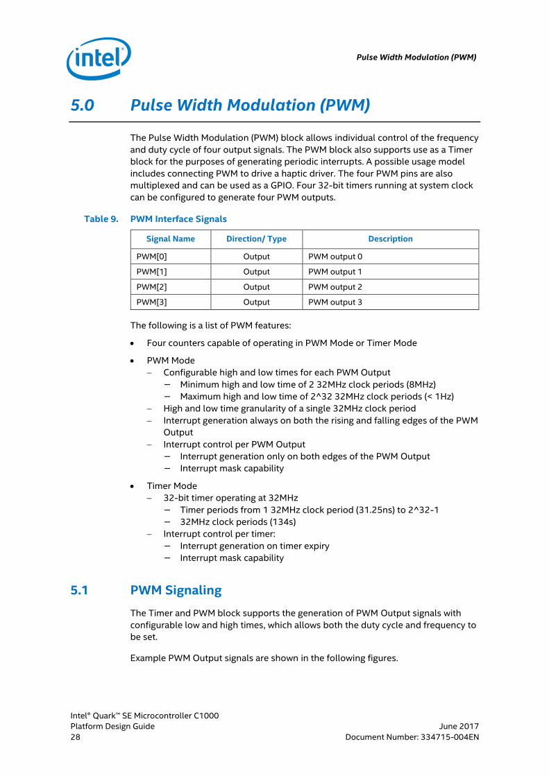
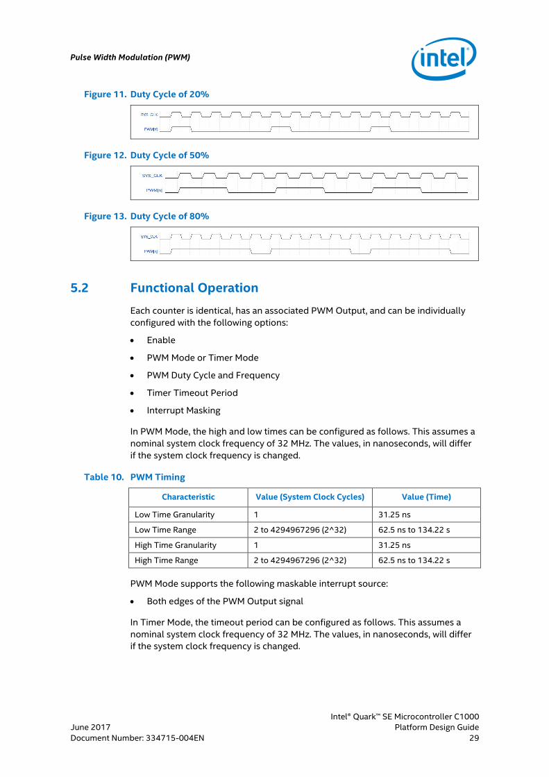
5.1 PWM Signaling
The Timer and PWM block supports the generation of PWM Output signals with
configurable low and high times, which allows both the duty cycle and frequency to
be set.
Example PWM Output signals are shown in the following figures.
Pulse Width Modulation (PWM)
Intel® Quark™ SE Microcontroller C1000
June 2017 Platform Design Guide
Document Number: 334715-004EN 29
Figure 11. Duty Cycle of 20%
Figure 12. Duty Cycle of 50%
Figure 13. Duty Cycle of 80%
5.2 Functional Operation
Each counter is identical, has an associated PWM Output, and can be individually
configured with the following options:
Enable
PWM Mode or Timer Mode
PWM Duty Cycle and Frequency
Timer Timeout Period
Interrupt Masking
In PWM Mode, the high and low times can be configured as follows. This assumes a
nominal system clock frequency of 32 MHz. The values, in nanoseconds, will differ
if the system clock frequency is changed.
Table 10. PWM Timing
Characteristic Value (System Clock Cycles) Value (Time)
Low Time Granularity 1 31.25 ns
Low Time Range 2 to 4294967296 (2^32) 62.5 ns to 134.22 s
High Time Granularity 1 31.25 ns
High Time Range 2 to 4294967296 (2^32) 62.5 ns to 134.22 s
PWM Mode supports the following maskable interrupt source:
Both edges of the PWM Output signal
In Timer Mode, the timeout period can be configured as follows. This assumes a
nominal system clock frequency of 32 MHz. The values, in nanoseconds, will differ
if the system clock frequency is changed.
Pulse Width Modulation (PWM)
Intel® Quark™ SE Microcontroller C1000
Platform Design Guide June 2017
30 Document Number: 334715-004EN
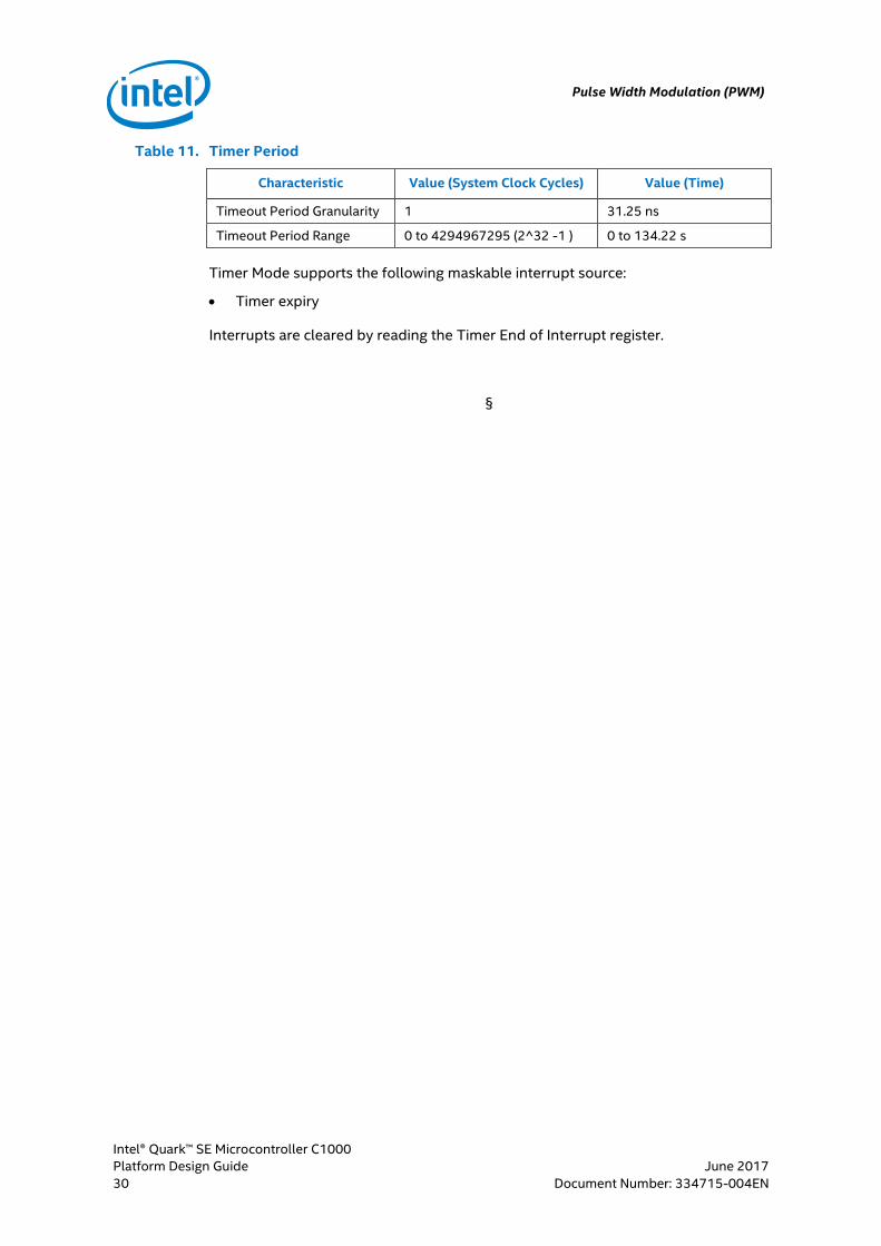
Table 11. Timer Period
Characteristic Value (System Clock Cycles) Value (Time)
Timeout Period Granularity 1 31.25 ns
Timeout Period Range 0 to 4294967295 (2^32 -1 ) 0 to 134.22 s
Timer Mode supports the following maskable interrupt source:
Timer expiry
Interrupts are cleared by reading the Timer End of Interrupt register.
§
UART
Intel® Quark™ SE Microcontroller C1000
June 2017 Platform Design Guide
Document Number: 334715-004EN 31
6.0 UART
UART is one of the hardware blocks in the Serial I/O (SIO).
The main features of the UART interface as follows:
Two 16550 compliant UART interfaces
Supports baud rates from 300 to 2M with less than 2% frequency error
Supports hardware and software flow control
FIFO mode support (16B TX and RX FIFOs)
Supports HW DMA with configurable FIFO thresholds
Supports 8-bit operation mode
Supports RS485 and RS232
Supports DTR/DCD/DSR/RI Modem Control Pins through GPIO pins controlled
by software
6.1 Signal Descriptions
Table 12. UART Signals
Signal Name Direction/ Type
Description
UART_x_TXD Output UART A single-ended Transmit data (RS232 or RS485). In RS485 mode, the differential driver is outside the SoC.
UART_x_RXD Input UART A single-ended Receive data (RS232 or RS485). In RS485 mode, the differential receiver is outside the SoC.
UART_x_RTS Output UART A Request to send (RS232)
UART_x_CTS Input UART A Clear to send (RS232)
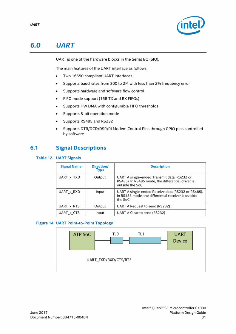
Figure 14. UART Point-to-Point Topology
TL0 TL1 UART Device
UART_TXD/RXD/CTS/RTS
ATP SoC
UART
Intel® Quark™ SE Microcontroller C1000
Platform Design Guide June 2017
32 Document Number: 334715-004EN
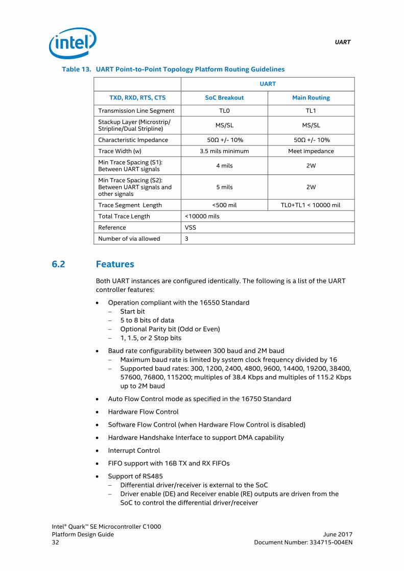
Table 13. UART Point-to-Point Topology Platform Routing Guidelines
UART
TXD, RXD, RTS, CTS SoC Breakout Main Routing
Transmission Line Segment TL0 TL1
Stackup Layer (Microstrip/ Stripline/Dual Stripline)
MS/SL MS/SL
Characteristic Impedance 50Ω +/- 10% 50Ω +/- 10%
Trace Width (w) 3.5 mils minimum Meet impedance
Min Trace Spacing (S1): Between UART signals
4 mils 2W
Min Trace Spacing (S2): Between UART signals and other signals
5 mils 2W
Trace Segment Length <500 mil TL0+TL1 < 10000 mil
Total Trace Length <10000 mils
Reference VSS
Number of via allowed 3
6.2 Features
Both UART instances are configured identically. The following is a list of the UART
controller features:
Operation compliant with the 16550 Standard
Start bit
5 to 8 bits of data
Optional Parity bit (Odd or Even)
1, 1.5, or 2 Stop bits
Baud rate configurability between 300 baud and 2M baud
Maximum baud rate is limited by system clock frequency divided by 16
Supported baud rates: 300, 1200, 2400, 4800, 9600, 14400, 19200, 38400,
57600, 76800, 115200; multiples of 38.4 Kbps and multiples of 115.2 Kbps
up to 2M baud
Auto Flow Control mode as specified in the 16750 Standard
Hardware Flow Control
Software Flow Control (when Hardware Flow Control is disabled)
Hardware Handshake Interface to support DMA capability
Interrupt Control
FIFO support with 16B TX and RX FIFOs
Support of RS485
Differential driver/receiver is external to the SoC
Driver enable (DE) and Receiver enable (RE) outputs are driven from the
SoC to control the differential driver/receiver
UART
Intel® Quark™ SE Microcontroller C1000
June 2017 Platform Design Guide
Document Number: 334715-004EN 33
Fractional clock divider that ensures less than 2% frequency error for most
supported baud rates
Fraction resolution is 4 bits
Exception: 2.07% error for 1.391 Mbaud, 2.12% for 1.882 Mbaud and
2Mbaud, 2.53% error for 1.684 Mbaud
§
SPI
Intel® Quark™ SE Microcontroller C1000
Platform Design Guide June 2017
34 Document Number: 334715-004EN
7.0 SPI
The Serial I/O implements two SPI controllers that support master mode and one
SPI controller that supports slave mode. Refer to the Intel® Quark™ SE
Microcontroller C1000 Datasheet for additional SPI compatibility requirements and
features. Support for SPI Flash devices is a key platform requirement and is needed
for all SoC designs.
Table 14. SPI Signals
Signal Name Direction/ Type Description
SPI_M_x_SCK Output SPI Serial Clock
SPI_M_x_CS_B[3:0] Output SPI Chip Select
SPI_M_x_MOSI Output SPI Master Output Slave Input
SPI_M_x_MISO Input SPI Master Input Slave Output
The Intel® Quark™ SE microcontroller C1000 includes the following:
Two SPI master interfaces with support for SPI clock frequencies up to 16 MHz
One SPI slave interface with support for SPI clock frequencies up to 3.2 MHz
Support for 4-bit up to 32-bit frame size
Up to four Slave Select pins per master interface
FIFO mode support (16B TX and RX FIFOs)
Support for HW DMA with configurable FIFO thresholds
7.1 Signal Descriptions
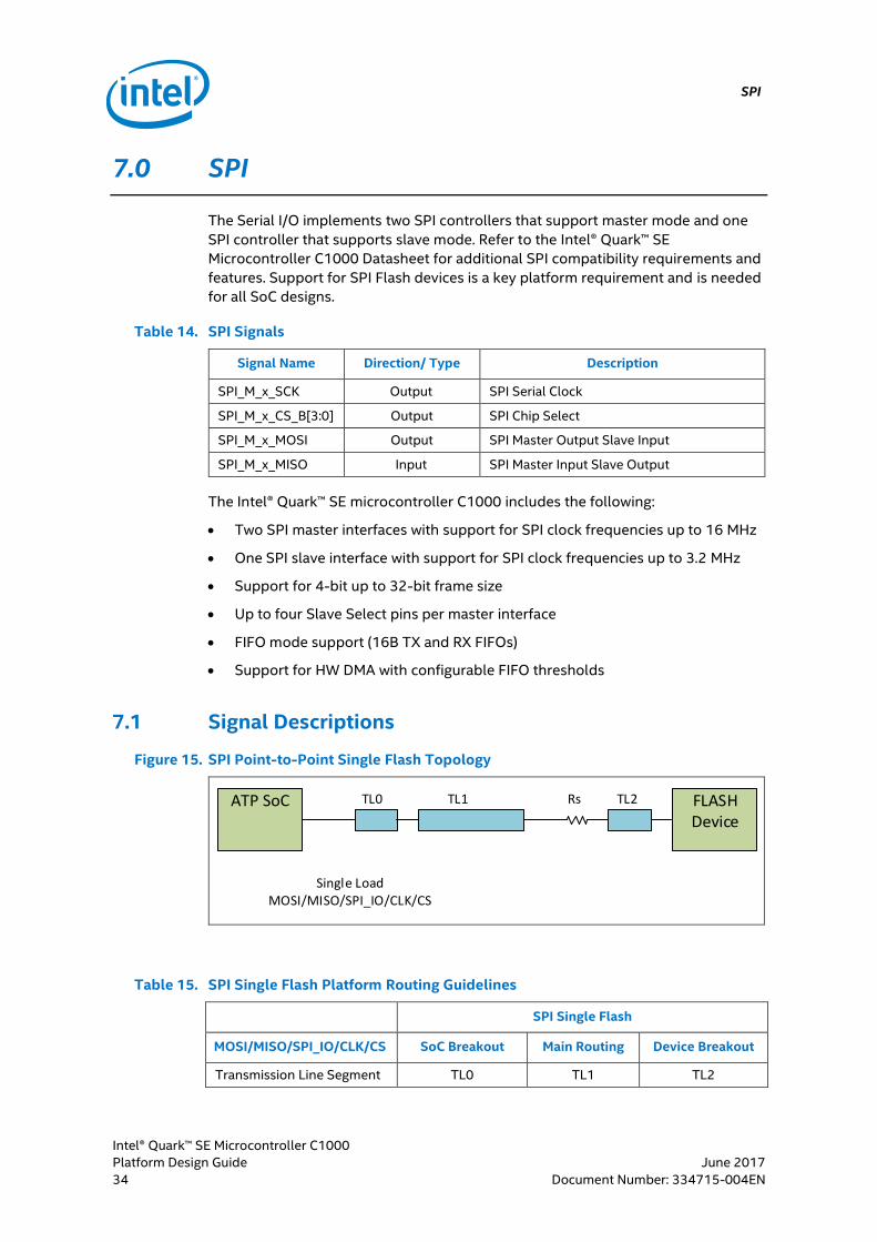
Figure 15. SPI Point-to-Point Single Flash Topology
TL0 TL1 TL2 FLASH Device
Single LoadMOSI/MISO/SPI_IO/CLK/CS
ATP SoC Rs
Table 15. SPI Single Flash Platform Routing Guidelines
SPI Single Flash
MOSI/MISO/SPI_IO/CLK/CS SoC Breakout Main Routing Device Breakout
Transmission Line Segment TL0 TL1 TL2
SPI
Intel® Quark™ SE Microcontroller C1000
June 2017 Platform Design Guide
Document Number: 334715-004EN 35
SPI Single Flash
MOSI/MISO/SPI_IO/CLK/CS SoC Breakout Main Routing Device Breakout
Routing Layer (Microstrip/Stripline/Dual Stripline)
MS/SL MS/SL MS/SL
Characteristic Impedance 50Ω +/- 10% 50Ω +/- 10% 50Ω +/- 10%
Trace Width (w) 3.5 mils minimum Meet
impedance Meet impedance
Trace Spacing (S1): Between SPI signals
4 mils 3W 2W
Trace Spacing (S2): Between SPI signals and other signals
5 mils 3W
2W
Trace Spacing(S3): Between SPI_CLK to other signals
5 mils 3W 2W
Trace Length <100 mils 1500 mils <
TL0+TL1+TL2 < 10000 mils
<500 mils
Length mismatch between SPI_CLK and SPI_CS
<250 mils
Length mismatch between SPI_CLK and DATA (SPI_IO/MOSI/MISO)
<250 mils
Trace Total Length 1500 mils < Total Length < 10000 mils
Number of vias allowed 4
Via stub length < 80 mils
Rs 33Ω
Reference VSS referencing
W W is the trace width
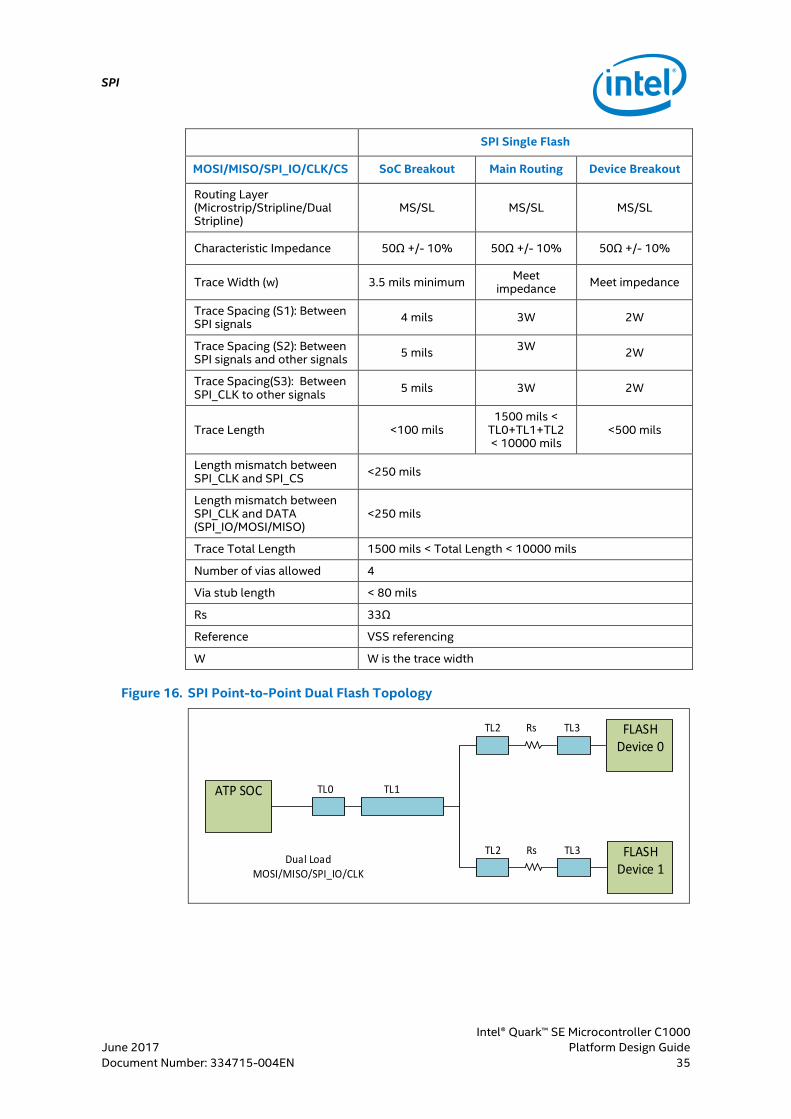
Figure 16. SPI Point-to-Point Dual Flash Topology
TL0 TL1
TL3 FLASH Device 0
Dual LoadMOSI/MISO/SPI_IO/CLK
ATP SOC
Rs
TL3 FLASH Device 1
Rs
TL2
TL2
SPI
Intel® Quark™ SE Microcontroller C1000
Platform Design Guide June 2017
36 Document Number: 334715-004EN
Table 16. SPI Dual Flash Platform Routing Guidelines
SPI Dual Flash
MOSI/MISO/SPI_IO/CLK SoC Breakout Main Routing T Branch
Routing Device
Breakout
Transmission Line Segment
TL0 TL1 TL2 TL3
Routing Layer (Microstrip/Stripline/Dual Stripline)
MS/SL MS/SL MS/SL MS/SL
Characteristic Impedance 50Ω +/- 10% 50Ω +/- 10% 50Ω +/- 10% 50Ω +/- 10%
Trace Width (w) 3.5 mils
minimum Meet
impedance Meet
impedance Meet
impedance
Trace Spacing (S1): Between SPI signals
4 mils 3W 3W 2W
Trace Spacing (S2): Between SPI signals and other signals
5 mils 3W 3W 2W
Trace Spacing(S3): Between SPI_CLK to other signals
5 mils 3W 3W 2W
Trace Length <100 mils
1500 mils < TL0+TL1+TL2+
TL3 < 8000 mils
TL2+TL3 < 2000 mils
<500 mils
Length mismatch between SPI_CLK and DATA (SPI_IO/MOSI/MISO)
<250 mils
Length mismatch between branches of same net
<100 mils
Trace Total Length 1500 mils < Total Length of Single Flash Device < 8000 mils
Number of vias allowed 4
Via stub length < 80 mils
Rs 33Ω
Reference VSS referencing
W W is the trace width
Figure 17. SPI_CS Point-to-Point Dual Flash Topology
TL0 TL1 TL2 FLASH Device
Dual Load SPI_CS
ATP SOC Rs
SPI
Intel® Quark™ SE Microcontroller C1000
June 2017 Platform Design Guide
Document Number: 334715-004EN 37
Table 17. SPI_CS Dual Flash Platform Routing Guidelines
SPI_CS Dual Flash
SPI_CS SoC Breakout Main Routing Device Breakout
Transmission Line Segment TL0 TL1 TL2
Routing Layer (Microstrip/Stripline/Dual Stripline)
MS/SL MS/SL MS/SL
Characteristic Impedance 50Ω +/- 10% 50Ω +/- 10% 50Ω +/- 10%
Trace Width (w) 3.5 mils minimum Meet
impedance Meet impedance
Trace Spacing (S1): Between SPI signals
4 mils 3W 2W
Trace Spacing (S2): Between SPI signals and other signals
5 mils 3W 2W
Trace Spacing(S3): Between SPI_CLK to other signals
5 mils 3W 2W
Trace Length <100 mils 1500 mils <
TL0+TL1+TL2 < 8000 mil
<500 mils
Length mismatch between SPI_CLK and SPI_CS
<250 mils
Length mismatch between SPI_CLK and DATA (SPI_IO/MOSI/MISO)
<250 mils
Length mismatch between branches of same net
<100 mils
Trace Total Length 1500 mils < Total Length of Single Flash Device < 8000 mils
Number of vias allowed 4
Via stub length < 80 mils
Rs 33Ω
Reference VSS referencing
W W is the trace width
7.2 Features
The following is a list of the SPI master features:
Two SPI master interfaces
Control of up to four Slave Selects
Frame formats:
Motorola* SPI
Texas Instruments* SSP
National Semiconductor Microwire*
Transfer modes:
SPI
Intel® Quark™ SE Microcontroller C1000
Platform Design Guide June 2017
38 Document Number: 334715-004EN
Transmit and Receive
Transmit Only
Receive Only
EEPROM Read
Serial clock frequencies up to 16 MHz
4-bit to 32-bit frame size
Configurable Clock Polarity and Clock Phase
Hardware Handshake Interface to support DMA capability
Interrupt Control
FIFO mode support with 16B deep TX and RX FIFOs
The following is a list of the SPI slave features:
One SPI slave interface
Frame formats:
Motorola* SPI
Texas Instruments* SSP
National Semiconductor Microwire*
Transfer modes:
Transmit and Receive
Transmit Only
Receive Only
EEPROM Read
Serial clock frequencies up to 3.2 MHz
4-bit to 32-bit frame size
Configurable Clock Polarity and Clock Phase
Hardware Handshake Interface to support DMA capability
Interrupt Control
FIFO mode support with 16B deep TX and RX FIFOs
§
Clocking
Intel® Quark™ SE Microcontroller C1000
June 2017 Platform Design Guide
Document Number: 334715-004EN 39
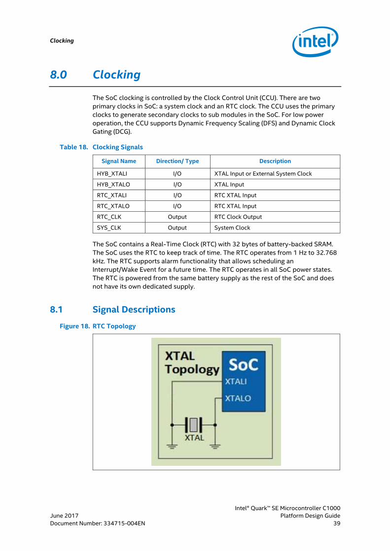
8.0 Clocking
The SoC clocking is controlled by the Clock Control Unit (CCU). There are two
primary clocks in SoC: a system clock and an RTC clock. The CCU uses the primary
clocks to generate secondary clocks to sub modules in the SoC. For low power
operation, the CCU supports Dynamic Frequency Scaling (DFS) and Dynamic Clock
Gating (DCG).
Table 18. Clocking Signals
Signal Name Direction/ Type Description
HYB_XTALI I/O XTAL Input or External System Clock
HYB_XTALO I/O XTAL Input
RTC_XTALI I/O RTC XTAL Input
RTC_XTALO I/O RTC XTAL Input
RTC_CLK Output RTC Clock Output
SYS_CLK Output System Clock
The SoC contains a Real-Time Clock (RTC) with 32 bytes of battery-backed SRAM.
The SoC uses the RTC to keep track of time. The RTC operates from 1 Hz to 32.768
kHz. The RTC supports alarm functionality that allows scheduling an
Interrupt/Wake Event for a future time. The RTC operates in all SoC power states.
The RTC is powered from the same battery supply as the rest of the SoC and does
not have its own dedicated supply.
8.1 Signal Descriptions
Figure 18. RTC Topology
Clocking
Intel® Quark™ SE Microcontroller C1000
Platform Design Guide June 2017
40 Document Number: 334715-004EN
Table 19. RTC Signals
Signal Name Direction/Type Description
OSC32_IN I Analog Crystal Input: This signal is connected to the 32.768 kHz Crystal
OSC32_OUT O Analog Crystal Output: This signal is connected to the 32.768 kHz Crystal
Table 20. RTC Point-to-Point Topology Platform Routing Guidelines
RTC Crystal
OSC32_IN/OSC32_OUT SoC Breakout Main Routing
Transmission Line Segment
TL1 TL2
Stackup Layer
(Microstrip/Stripline) MS/SL MS/SL
Characteristic Impedance (SE)
50Ω +/- 10% 50Ω +/- 10%
Trace Width (w) Meet impedance Meet impedance
Trace Spacing (S):
to other signals 15 mils 25 mils
Trace Length < 250 mils
Total Trace Length Total Length < 1000 mils
Number of vias allowed 2
Via stub length < 20 mils
Guidelines
Reduce trace capacitance by minimizing the RTC trace length.
Reduce trace signal coupling by avoiding the routing of high speed signals
close to RTC signals.
We highly recommend that you use a ground guard plane.
Do not route RTC as differential signals.
Table 21. 32Mhz Crystal Oscillator specification
Symbol Parameter Min. Typ. Max. Unit
Fo Crystal frequency 32 32 32 Mhz
Cesr Crystal ESR 12.68 14.41 50 Ω
Cm Crystal Motional Cap 3.34 3.54 pF
Co Crystal Shunt Cap 0.84 1.5 pF
CL Crystal Load Cap 10 pF
Ftol Frequency Tolerance -30 30 ppm
Dlev Drive Level (25Ω) 10 uW
Clocking
Intel® Quark™ SE Microcontroller C1000
June 2017 Platform Design Guide
Document Number: 334715-004EN 41
Table 22. 32Khz Crystal Oscillator specification
Symbol Parameter Min Typ Max Unit
Fo Crystal frequency 32,768 Hz
Cesr Crystal ESR 50 80 KΩ
Cm Crystal Motional Cap 3.7 pF
Co Crystal Shunt Cap 1.2 pF
CL Crystal Load Cap 7 pF
Ftol Frequency Tolerance -20 20 ppm
Dlev Drive Level 1 uW
8.2 Features
The following is a list of the RTC features:
Programmable 32-bit binary counter
Counter increments on successive edges of a Counter Clock from 1 Hz to
32.768 kHz (derived from the 32.768 kHz Crystal Oscillator clock)
Comparator for Interrupt/Wake Event generation based on the programmed
Match Value
Support for Interrupt/Wake Event generation when only the Counter Clock is
running (Fabric Clock is off)
§
General Purpose I/O (GPIO)
Intel® Quark™ SE Microcontroller C1000
Platform Design Guide June 2017
42 Document Number: 334715-004EN
9.0 General Purpose I/O (GPIO)
The SoC contains GPIO pins and the interfaces can be active at different times. To
provide maximum flexibility at the lowest cost point, some GPIO pins are
shared/muxed among various interfaces. BIOS is responsible for enabling proper
configuration. The SoC contains two instances of the GPIO controller.
The GPIO controller provides a total of 32 independently configurable GPIOs:
All GPIOs are interrupt capable, supporting level sensitive and edge triggered
modes
All GPIOs support Debounce logic for interrupt sources
All 32 GPIOs are Always-on interrupt and wake capable
There are 16 additional GPIOs available via the Sensor Subsystem.
9.1 Signal Descriptions
Table 23. GPIO Signals
Signal Name Direction/Type Description
GPIO[31:0] I/O 32 General Purpose IO’s
Figure 19. GPIO Pin Routing Topology
General Purpose I/O (GPIO)
Intel® Quark™ SE Microcontroller C1000
June 2017 Platform Design Guide
Document Number: 334715-004EN 43
Table 24. GPIO Pin Routing Guidelines
GPIO
GPIO (MV to GPIO Header/Device) BRK OUT Main BRK IN
Transmission Line Segment L1 L2 L3
Routing Layer (Microstrip/Stripline)
MS/SL MS/SL MS/SL
Characteristic Impedance 50Ω + 10% (MS) 50Ω + 10% (SL)
50Ω + 10% (MS) 50Ω + 10% (SL)
50Ω + 10% (MS) 50Ω + 10% (SL)
Trace Width (w) Meet impedance Meet impedance Meet impedance
Trace Spacing (S): Between SPI signals
5 mils minimum 2W 5 mils minimum
Trace Spacing (S2): Between SPI signals and other signals
5 mils minimum 3W 5 mils minimum
Trace Length 0.5" max 9" max 0.5" max
Trace Total Length Total trace length = 10" max
1. Rs = 22 or 33Ω ideally closer to driver
2. The modelled GPIO device is 30pF; GPIOs can drive higher loads at reduced lengths
3. Maximum speed = 8 MHz
9.2 Features
The following is a list of the GPIO controller features:
32 independently configurable GPIOs
6 additional AON GPIOs
Separate data register bit and data direction control bit for each GPIO
Metastability registers for GPIO read data
Interrupt mode supported for all GPIOs, configurable as follows:
Active High Level
Active Low Level
Rising Edge
Falling Edge
Both Edge
Debounce logic for interrupt sources
§
JTAG
Intel® Quark™ SE Microcontroller C1000
Platform Design Guide June 2017
44 Document Number: 334715-004EN
10.0 JTAG
This section provides JTAG related information.
10.1 Signal Descriptions
Figure 20. JTAG Topology
Intel® Quark SE
SoC
Debug connector
TDO
VREF_DEBUG
R2L1 Lterm2
TDI/TMS/TCK
VREF_DEBUG
R1Lterm1 L1
Table 25. Generic Routing Requirements
JTAG
TDO/TDI/TMS/TCK Main Routing Termination Route for TDO
Termination Route for
TDI/TMS/TCK
Transmission Line Segment TL1 TLterm2 TLterm1
Routing Layer (Microstrip/Stripline/Dual Stripline)
MS/SL MS/SL MS/SL
Characteristic Impedance (SE) 50Ω +/- 10% 50Ω +/- 10% 50Ω +/- 10%
Trace Width (w) Meet impedance Meet impedance Meet
impedance
Trace Spacing(S): Both between JTAG signals and to other signals
3W 3W 3W
Trace Length L1 + Lterm(1/2)
<5500 mils <250 mils <1100 mil
Total Trace Length <5500 mils
Max unterminated stub length
<1100 mil
Length mismatch between DATA and TCK
<250 mil
Reference VSS referencing
Termination R1 = 51 Ω +/- 5%; R2 = 51 Ω +/- 5%
JTAG
Intel® Quark™ SE Microcontroller C1000
June 2017 Platform Design Guide
Document Number: 334715-004EN 45
10.2 Features
The following is a list of the JTAG Interface features:
5-pin IEEE 1149.1 JTAG Interface
Boundary scan support
ARC metaware debugger
LMT minutia debugger
§
Analog-to-Digital Converter (ADC)
Intel® Quark™ SE Microcontroller C1000
Platform Design Guide June 2017
46 Document Number: 334715-004EN
11.0 Analog-to-Digital Converter (ADC)
The Sensor Subsystem contains an analog-to-digital converter (ADC) controller.
The ADC controller is responsible for gathering samples from the ADC block. It
generates control to the ADC to acquire the samples and stores the received
samples in a FIFO for retrieval by the ARC core.
Table 26. ADC Signals
Signal Name Direction/Type Description
AI[19:1] Analog Input 19 Analog Input Channels
11.1 Signal Descriptions
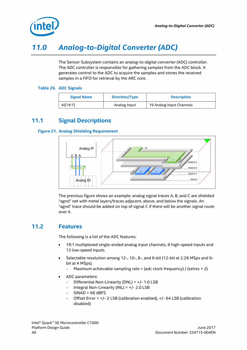
Figure 21. Analog Shielding Requirement
The previous figure shows an example: analog signal traces A, B, and C are shielded
“agnd” net with metal layers/traces adjacent, above, and below the signals. An
“agnd” trace should be added on top of signal C if there will be another signal route
over it.
11.2 Features
The following is a list of the ADC features:
19:1 multiplexed single-ended analog input channels, 6 high-speed inputs and
13 low-speed inputs.
Selectable resolution among 12-, 10-, 8-, and 6-bit (12-bit at 2.28 MSps and 6-
bit at 4 MSps).
Maximum achievable sampling rate = (adc clock frequency) / (selres + 2)
ADC parameters:
Differential Non-Linearity (DNL) = +/- 1.0 LSB
Integral Non-Linearity (INL) = +/- 2.0 LSB
SINAD = 68 dBFS
Offset Error = +/- 2 LSB (calibration enabled), +/- 64 LSB (calibration
disabled)
Analog-to-Digital Converter (ADC)
Intel® Quark™ SE Microcontroller C1000
June 2017 Platform Design Guide
Document Number: 334715-004EN 47
Latencies:
Power-up time of <= 10 us
1 conversion cycle = (resolution bits + 2) cycles
Full-scale input range is 0 to AVDD.
ADC Reference Voltage (Vrefp) of ADC HIP is connected to AVDD.
§
USB
Intel® Quark™ SE Microcontroller C1000
Platform Design Guide June 2017
48 Document Number: 334715-004EN
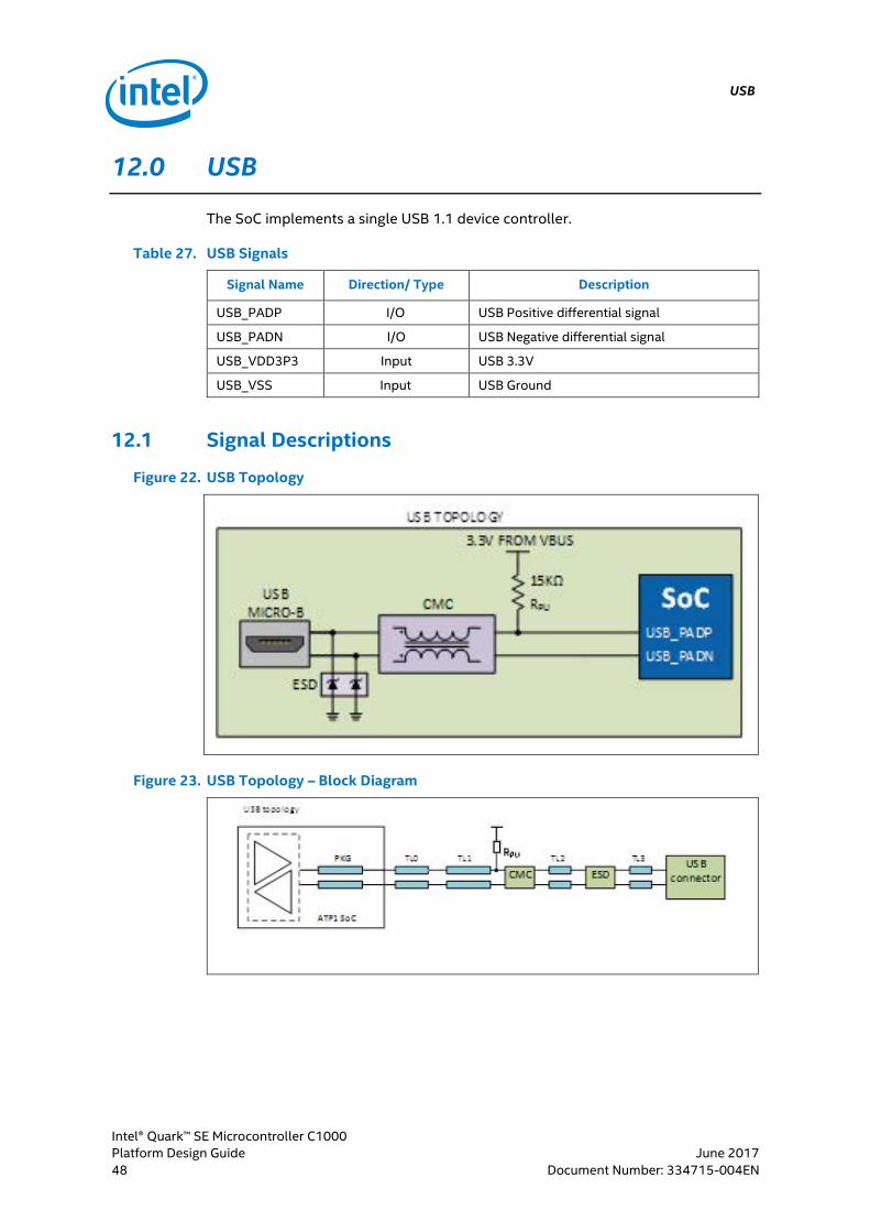
12.0 USB
The SoC implements a single USB 1.1 device controller.
Table 27. USB Signals
Signal Name Direction/ Type Description
USB_PADP I/O USB Positive differential signal
USB_PADN I/O USB Negative differential signal
USB_VDD3P3 Input USB 3.3V
USB_VSS Input USB Ground
12.1 Signal Descriptions
Figure 22. USB Topology
Figure 23. USB Topology – Block Diagram
USB
Intel® Quark™ SE Microcontroller C1000
June 2017 Platform Design Guide
Document Number: 334715-004EN 49
Table 28. USB Routing Requirements
USB
USB_DP/DN SoC Breakout Main Routing CMC and ESD routing
Transmission Line Segment TL0 TL1 TL2 & TL3
Routing Layer (Microstrip/Stripline/Dual Stripline)
MS/SL MS/SL MS
Characteristic Impedance (Differential)
90Ω +/- 10% 90Ω +/- 10% 90Ω +/- 10%
Trace Width (w) 4 mils minimum Meet impedance Meet
impedance
Trace Spacing (S): Between P and N within a diff pair
4 mils minimum Meet impedance Meet
impedance
Trace Spacing(S1): Between USB pairs
4 mils minimum max (15 mils or
3H) max (15 mils or
3H)
Trace Spacing (S2): Between diff pairs and other signals
4H max (25 mils or
5H) max (25 mils or
5H)
Trace Spacing(S3): Between diff pairs and high speed CLK signals
4H 50 mils 50 mils
Trace Length <200 mils TL0 + TL1 + TL2
+ TL3 < 7500 mils
TL2+TL3 < 500 mils
Length mismatch between P and N of same pair
<10 mils
Length mismatch between pairs
Not required
Total Trace Length Total Length < 7500 mil
Number of vias allowed 4
Via stub length < 80 mils
Cable length supported (front panel)
9 inch
Rs 33 Ω
Reference VSS referencing; No plane split allowed
H H is the distance to the nearest reference plane
12.2 Features
The following is a list of the USB controller features:
Supports USB 1.1 Full speed only (12 Mbps)
Supports internal DMA
Buffer mode DMA supported (scatter gather mode is not supported)
DMA control per endpoint per direction supported
Generates DMA interrupt after a configurable number of bytes/packets
have been transmitted
USB
Intel® Quark™ SE Microcontroller C1000
Platform Design Guide June 2017
50 Document Number: 334715-004EN
Supports one control endpoint
Supports three bidirectional endpoints (in addition to control end point)
Supports two IN endpoints
Supports control, interrupt and bulk transfers (does not support isochronous
transfers)
Supports a maximum packet size of 64 bytes
Supports dedicated FIFOs per IN endpoint
Each Transmit FIFO is sized at two maximum sized packets
Each Transmit FIFO can be filled with minimum sized packets
Supports a single FIFO for all OUT end points
The receive FIFO is sized at two maximum sized packets
The receive FIFO can be filled with minimum sized packets
§
Power
Intel® Quark™ SE Microcontroller C1000
June 2017 Platform Design Guide
Document Number: 334715-004EN 51
13.0 Power
The Intel® Quark™ SE SoC-based platform has the option to use either internal
regulators from the SoC or external power sources from the platform. This chapter
provides information about how to configure both internal and external voltage
regulators (VRs).
13.1 Configuration for External VR
During power-up, the SoC determines the platform VR usage (whether internal or
external) based on the PLT_REG_EN strap signal status. The SoC has two distinctive
power up sequences for both internal and external platform power up options.
Once the SoC identifies the PLT_REG_EN status, the SoC follows the appropriate
power up sequencing for the platform power supply selected by the design. The
details of these power up sequences are documented in the Intel® Quark™ SE
Microcontroller C1000 Datasheet.
The following steps provide guidelines for configuring the SoC when an external
platform power source is required:
1. Tie the strap pin PLT_REG_EN to the VCC_AVD_OPM_2P6 power rail. This
voltage is an output from the SoC (VCCOUT_AVD_OPM_2P6).
Caution: Special care must be taken in the event of a hardware power down of
VCC_BATT_OPM_3P7 followed by a power up sequence. Please ensure that the
Intel® Quark™ SE Microcontroller C1000 reference voltage OPM_2P6 is
discharged to ground before a power up cycle. For suggestions on how to
ensure the correct voltage levels in VCC_AVD_OPM_2P6 at any time, refer to
the Intel® Quark™ SE Microcontroller C1000 Power Sequencing Considerations
Application Note.
2. Connect VCCOUT_QLR1_3P3 and VCCOUT_QLR2_1P8 to reference plane
(GND).
3. Connect VCC_VSENSE_PLAT_3P3 and VCC_VSENSE_PLAT_1P8 to reference
plane (GND).
4. Connect VSS_GNDSENSE_ESR1 and VSS_GNDSENSE_ESR2 to reference plane
(GND).
5. Leave the VCCOUT_PLAT_3P3_3P3 and VCCOUT_PLAT_1P8_1P8 pins
unconnected.
Note: If the system needs to support sleep state, the external power supply that is
connected to the VCC_AON_1P8 pin must be active (always on) while the system
goes into sleep mode.
The following figures depict the steps outlined above.
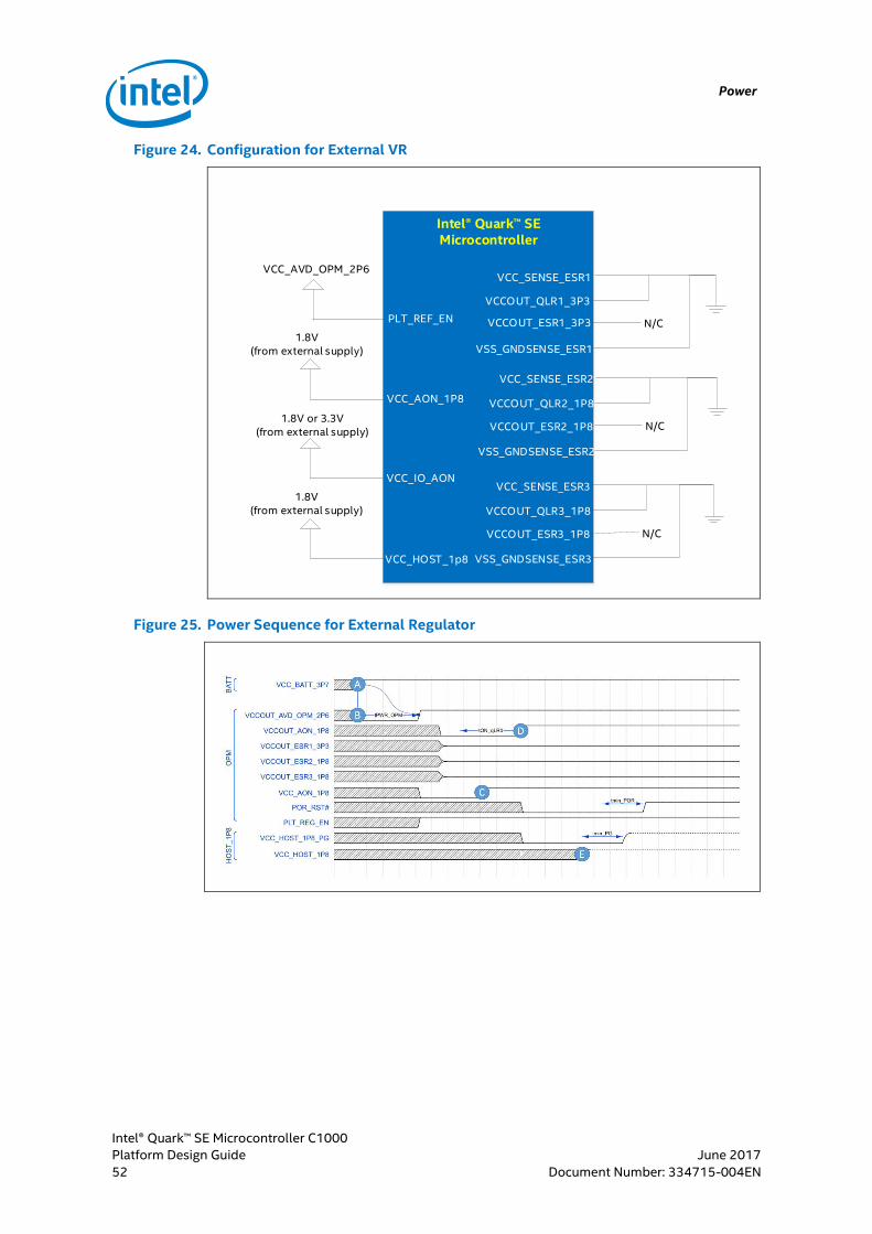
Power
Intel® Quark™ SE Microcontroller C1000
Platform Design Guide June 2017
52 Document Number: 334715-004EN
Figure 24. Configuration for External VR
N/C
N/C
Intel® Quark SE Microcontroller
PLT_REF_EN
VCC_SENSE_ESR1
VCCOUT_QLR1_3P3
VCCOUT_ESR1_3P3
VSS_GNDSENSE_ESR1
VCC_SENSE_ESR3
VCCOUT_QLR3_1P8
VCCOUT_ESR3_1P8
VSS_GNDSENSE_ESR3
VCC_AVD_OPM_2P6
VCC_IO_AON
VCC_AON_1P8
1.8V (from external supply)
1.8V or 3.3V(from external supply)
VCC_HOST_1p8
1.8V (from external supply)
N/C
VCC_SENSE_ESR2
VCCOUT_QLR2_1P8
VCCOUT_ESR2_1P8
VSS_GNDSENSE_ESR2
Figure 25. Power Sequence for External Regulator
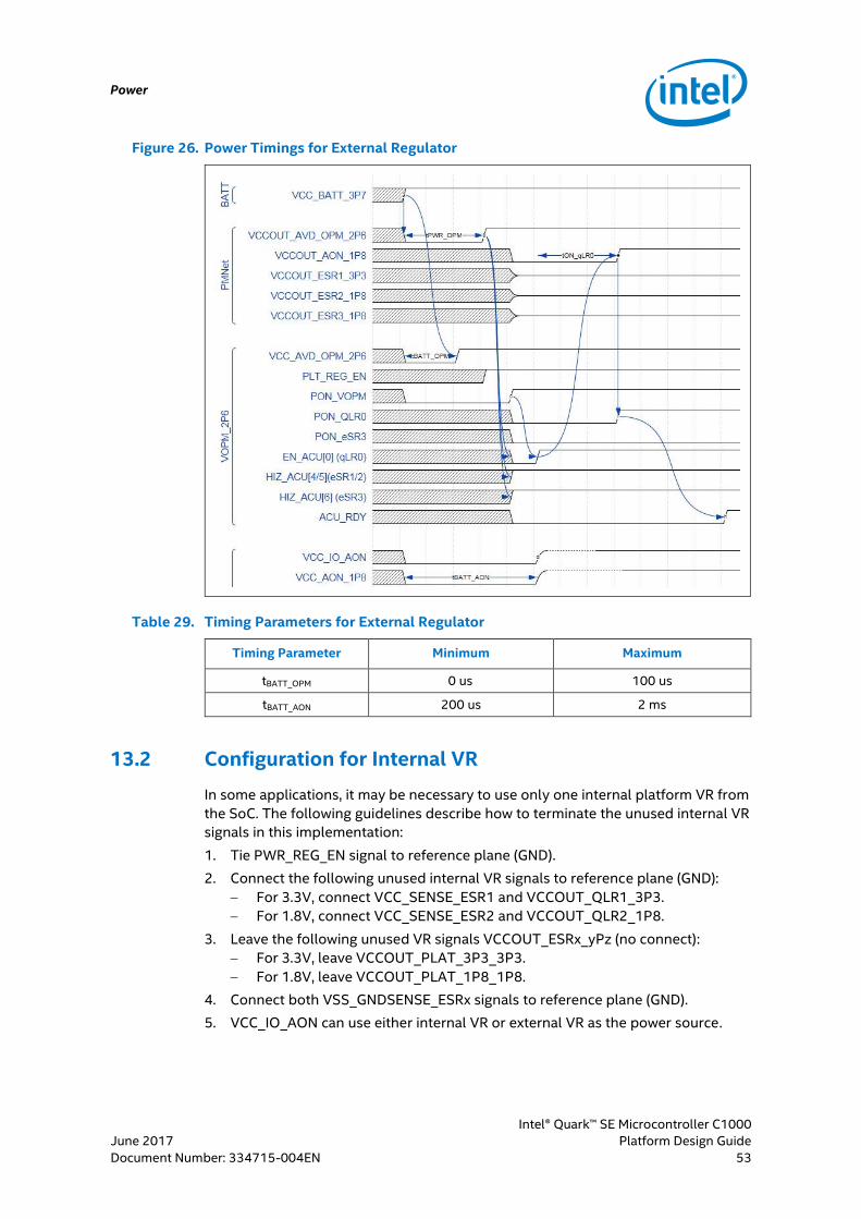
Power
Intel® Quark™ SE Microcontroller C1000
June 2017 Platform Design Guide
Document Number: 334715-004EN 53
Figure 26. Power Timings for External Regulator
Table 29. Timing Parameters for External Regulator
Timing Parameter Minimum Maximum
tBATT_OPM 0 us 100 us
tBATT_AON 200 us 2 ms
13.2 Configuration for Internal VR
In some applications, it may be necessary to use only one internal platform VR from
the SoC. The following guidelines describe how to terminate the unused internal VR
signals in this implementation:
1. Tie PWR_REG_EN signal to reference plane (GND).
2. Connect the following unused internal VR signals to reference plane (GND):
For 3.3V, connect VCC_SENSE_ESR1 and VCCOUT_QLR1_3P3.
For 1.8V, connect VCC_SENSE_ESR2 and VCCOUT_QLR2_1P8.
3. Leave the following unused VR signals VCCOUT_ESRx_yPz (no connect):
For 3.3V, leave VCCOUT_PLAT_3P3_3P3.
For 1.8V, leave VCCOUT_PLAT_1P8_1P8.
4. Connect both VSS_GNDSENSE_ESRx signals to reference plane (GND).
5. VCC_IO_AON can use either internal VR or external VR as the power source.
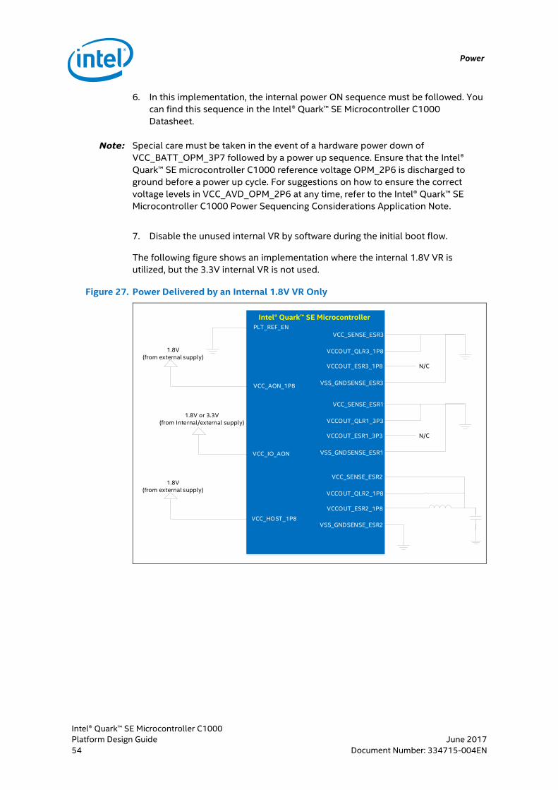
Power
Intel® Quark™ SE Microcontroller C1000
Platform Design Guide June 2017
54 Document Number: 334715-004EN
6. In this implementation, the internal power ON sequence must be followed. You
can find this sequence in the Intel® Quark™ SE Microcontroller C1000
Datasheet.
Note: Special care must be taken in the event of a hardware power down of
VCC_BATT_OPM_3P7 followed by a power up sequence. Ensure that the Intel®
Quark™ SE microcontroller C1000 reference voltage OPM_2P6 is discharged to
ground before a power up cycle. For suggestions on how to ensure the correct
voltage levels in VCC_AVD_OPM_2P6 at any time, refer to the Intel® Quark™ SE
Microcontroller C1000 Power Sequencing Considerations Application Note.
7. Disable the unused internal VR by software during the initial boot flow.
The following figure shows an implementation where the internal 1.8V VR is
utilized, but the 3.3V internal VR is not used.
Figure 27. Power Delivered by an Internal 1.8V VR Only
N/C
Intel® Quark SE Microcontroller
PLT_REF_EN
VCC_SENSE_ESR1
VCCOUT_QLR1_3P3
VCCOUT_ESR1_3P3
VSS_GNDSENSE_ESR1
VCC_SENSE_ESR2
VCCOUT_QLR2_1P8
VCCOUT_ESR2_1P8
VSS_GNDSENSE_ESR2
VCC_IO_AON
VCC_AON_1P8
1.8V or 3.3V(from Internal/external supply)
1.8V (from external supply)
VCC_HOST_1P8
1.8V (from external supply)
N/C
VCC_SENSE_ESR3
VCCOUT_QLR3_1P8
VCCOUT_ESR3_1P8
VSS_GNDSENSE_ESR3
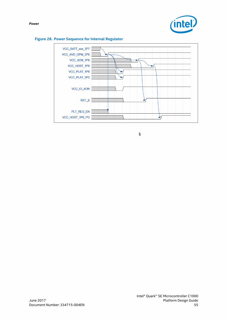
Power
Intel® Quark™ SE Microcontroller C1000
June 2017 Platform Design Guide
Document Number: 334715-004EN 55
Figure 28. Power Sequence for Internal Regulator
§
Termination of Unused Pins
Intel® Quark™ SE Microcontroller C1000
Platform Design Guide June 2017
56 Document Number: 334715-004EN
14.0 Termination of Unused Pins
14.1 Guidelines for Terminating Unused Pins
Leaving unused input pins floating is not an ideal solution in any design. Floating
pins, either analog or digital, can pick up surrounding electromagnetic or
electrostatic signals and then oscillate, which can draw current, leading to
unnecessary heating and power supply drain. This also affects signals on other pins
if they are configured as inputs. Therefore, we recommend that you terminate
unused pins to minimize the current flows and signal distortions.
In general, unused analog or digital input pins should be connected to ground or
power supply through 1 - 10 kΩ pull (pull-down or pull-up) resistors. Making the
resistors too large exposes circuits to external influences, such as RF or electric
fields. Unused output pins can be left unconnected, unless special circumstances
require otherwise.
Where possible, pull pins down to ground. Shorts are more likely to occur to
ground, and this reduces coupling of power supply noise to that point in the circuit.
Those pins should also be initiated as inputs, or in high resistance states, to avoid
shorted outputs implications.
Pulling down to VSS consumes about 15% less power than pulling up to VCC for
CMOS technology based components.
The following sections describe the methods of termination recommended for the
Intel® Quark™ SE microcontroller C1000, according to the types of unused pins.
14.2 Termination of Unused Pins for Intel® Quark™ SE Microcontroller C1000
The Intel® Quark™ SE microcontroller C1000 supports multiplexing, therefore, its
pins are assigned with functions. For information about the assignment of SoC
balls/pins to functions, see Section 2.4, “Pin Mapping”. Function_0 is assigned to
each ball/pin by default, and initiated during boot up flow. Unless the bootloader
configuration has been changed, only pins assigned to Function_0 will be subject
for termination, as Function_1 and Function_2 are not activated during start up.
14.2.1 GPIO Pin Termination
All GPIO pins are configured as inputs on power-up or the assertion of a system
reset. Pins configured this way are in a high-impedance state. Therefore, unused
GPIO pins could be terminated by pulling them down to VSS through, for example,
a 10 kΩ resistor. Figure 29 illustrates the termination of the GPIO_9_SPI1_M_MISO
pin (ball B6). This analogy should apply to terminating any other GPIO pins,
including the Always ON GPIO and Sensor Subsystem GPIO pins.
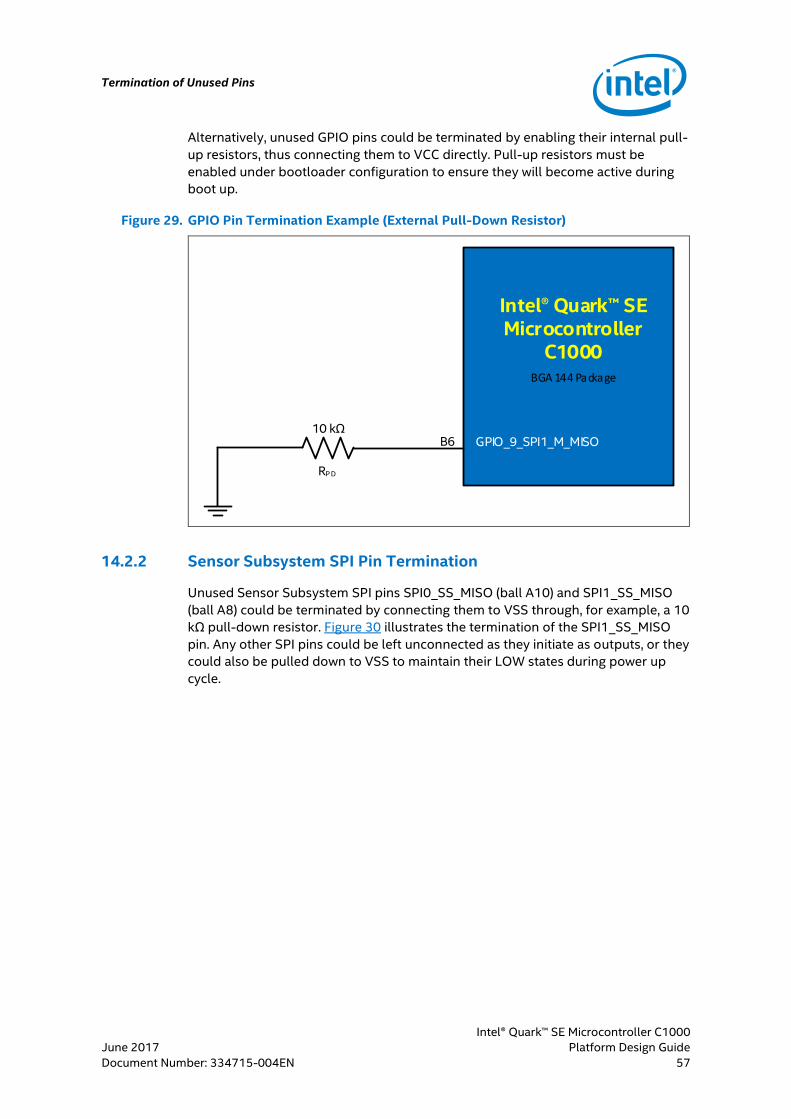
Termination of Unused Pins
Intel® Quark™ SE Microcontroller C1000
June 2017 Platform Design Guide
Document Number: 334715-004EN 57
Alternatively, unused GPIO pins could be terminated by enabling their internal pull-
up resistors, thus connecting them to VCC directly. Pull-up resistors must be
enabled under bootloader configuration to ensure they will become active during
boot up.
Figure 29. GPIO Pin Termination Example (External Pull-Down Resistor)
GPIO_9_SPI1_M_MISOB610 kΩ
RP D
Intel® Quark SE Microcontroller
C1000BGA 144 Package
14.2.2 Sensor Subsystem SPI Pin Termination
Unused Sensor Subsystem SPI pins SPI0_SS_MISO (ball A10) and SPI1_SS_MISO
(ball A8) could be terminated by connecting them to VSS through, for example, a 10
kΩ pull-down resistor. Figure 30 illustrates the termination of the SPI1_SS_MISO
pin. Any other SPI pins could be left unconnected as they initiate as outputs, or they
could also be pulled down to VSS to maintain their LOW states during power up
cycle.
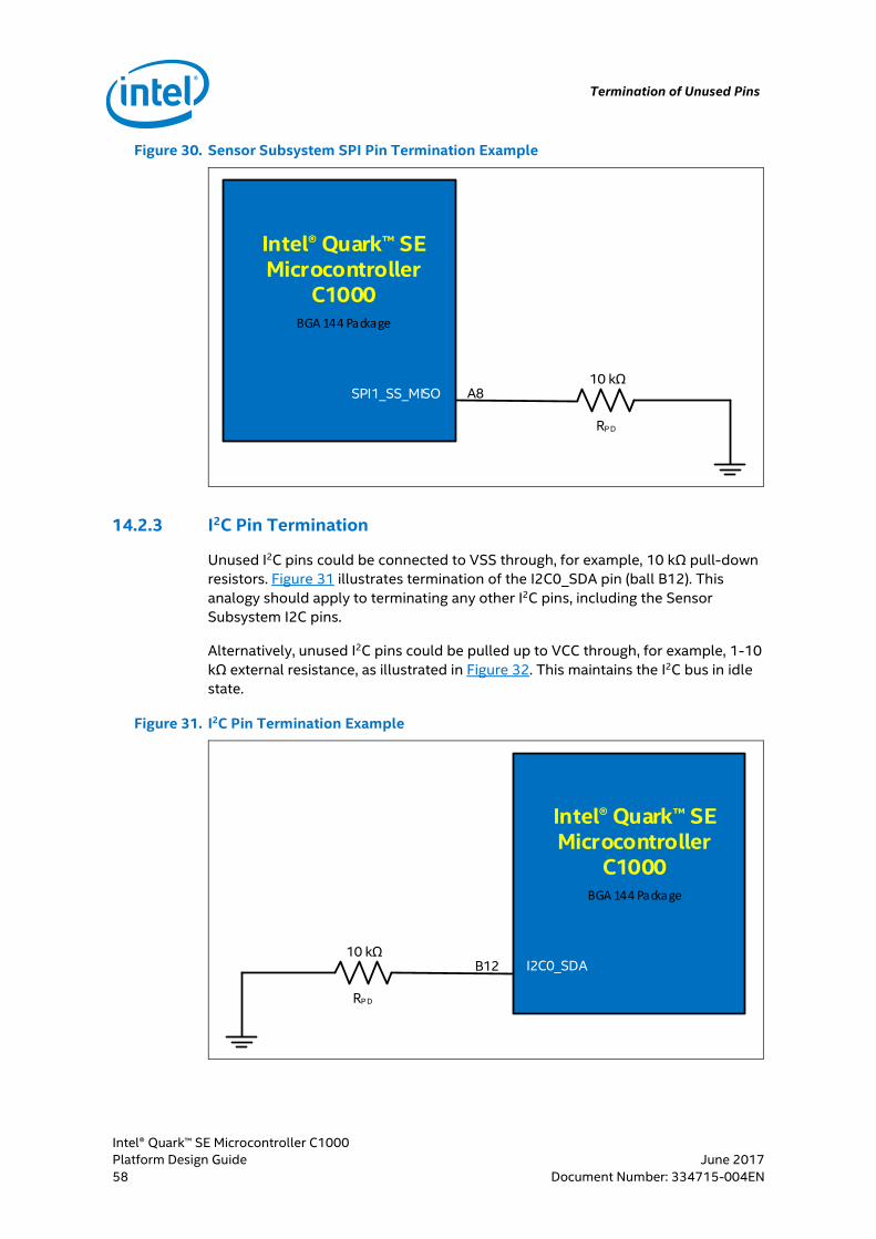
Termination of Unused Pins
Intel® Quark™ SE Microcontroller C1000
Platform Design Guide June 2017
58 Document Number: 334715-004EN
Figure 30. Sensor Subsystem SPI Pin Termination Example
SPI1_SS_MISO A8
Intel® Quark SE Microcontroller
C1000BGA 144 Package
10 kΩ
RP D
14.2.3 I2C Pin Termination
Unused I2C pins could be connected to VSS through, for example, 10 kΩ pull-down
resistors. Figure 31 illustrates termination of the I2C0_SDA pin (ball B12). This
analogy should apply to terminating any other I2C pins, including the Sensor
Subsystem I2C pins.
Alternatively, unused I2C pins could be pulled up to VCC through, for example, 1-10
kΩ external resistance, as illustrated in Figure 32. This maintains the I2C bus in idle
state.
Figure 31. I2C Pin Termination Example
B1210 kΩ
RP D
Intel® Quark SE Microcontroller
C1000BGA 144 Package
I2C0_SDA
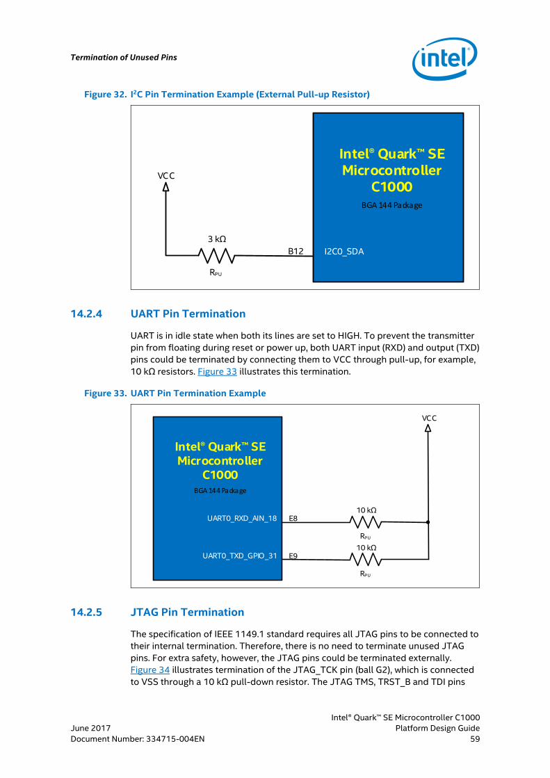
Termination of Unused Pins
Intel® Quark™ SE Microcontroller C1000
June 2017 Platform Design Guide
Document Number: 334715-004EN 59
Figure 32. I2C Pin Termination Example (External Pull-up Resistor)
I2C0_SDAB12
3 kΩ
RPU
Intel® Quark SE Microcontroller
C1000BGA 144 Package
VCC
14.2.4 UART Pin Termination
UART is in idle state when both its lines are set to HIGH. To prevent the transmitter
pin from floating during reset or power up, both UART input (RXD) and output (TXD)
pins could be terminated by connecting them to VCC through pull-up, for example,
10 kΩ resistors. Figure 33 illustrates this termination.
Figure 33. UART Pin Termination Example
UART0_RXD_AIN_18 E8
Intel® Quark SE Microcontroller
C1000BGA 144 Package
10 kΩ
RPU
UART0_TXD_GPIO_3110 kΩ
RPU
E9
VCC
14.2.5 JTAG Pin Termination
The specification of IEEE 1149.1 standard requires all JTAG pins to be connected to
their internal termination. Therefore, there is no need to terminate unused JTAG
pins. For extra safety, however, the JTAG pins could be terminated externally.
Figure 34 illustrates termination of the JTAG_TCK pin (ball G2), which is connected
to VSS through a 10 kΩ pull-down resistor. The JTAG TMS, TRST_B and TDI pins
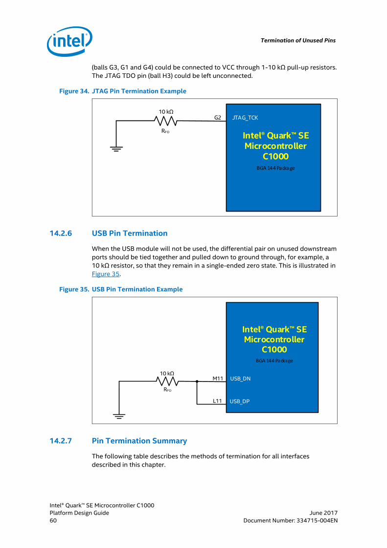
Termination of Unused Pins
Intel® Quark™ SE Microcontroller C1000
Platform Design Guide June 2017
60 Document Number: 334715-004EN
(balls G3, G1 and G4) could be connected to VCC through 1-10 kΩ pull-up resistors.
The JTAG TDO pin (ball H3) could be left unconnected.
Figure 34. JTAG Pin Termination Example
JTAG_TCKG210 kΩ
RP D
Intel® Quark SE Microcontroller
C1000BGA 144 Package
14.2.6 USB Pin Termination
When the USB module will not be used, the differential pair on unused downstream
ports should be tied together and pulled down to ground through, for example, a
10 kΩ resistor, so that they remain in a single-ended zero state. This is illustrated in
Figure 35.
Figure 35. USB Pin Termination Example
USB_DNM1110 kΩ
RP D
Intel® Quark SE Microcontroller
C1000BGA 144 Package
USB_DPL11
14.2.7 Pin Termination Summary
The following table describes the methods of termination for all interfaces
described in this chapter.
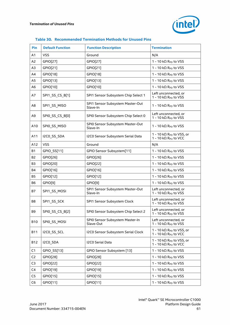
Termination of Unused Pins
Intel® Quark™ SE Microcontroller C1000
June 2017 Platform Design Guide
Document Number: 334715-004EN 61
Table 30. Recommended Termination Methods for Unused Pins
Pin Default Function Function Description Termination
A1 VSS Ground N/A
A2 GPIO[27] GPIO[27] 1 - 10 kΩ RPD to VSS
A3 GPIO[21] GPIO[21] 1 - 10 kΩ RPD to VSS
A4 GPIO[18] GPIO[18] 1 - 10 kΩ RPD to VSS
A5 GPIO[13] GPIO[13] 1 - 10 kΩ RPD to VSS
A6 GPIO[10] GPIO[10] 1 - 10 kΩ RPD to VSS
A7 SPI1_SS_CS_B[1] SPI1 Sensor Subsystem Chip Select 1 Left unconnected, or 1 - 10 kΩ RPD to VSS
A8 SPI1_SS_MISO SPI1 Sensor Subsystem Master-Out Slave-In
1 - 10 kΩ RPD to VSS
A9 SPI0_SS_CS_B[0] SPI0 Sensor Subsystem Chip Select 0 Left unconnected, or 1 - 10 kΩ RPD to VSS
A10 SPI0_SS_MISO SPI0 Sensor Subsystem Master-Out Slave-In
1 - 10 kΩ RPD to VSS
A11 I2C0_SS_SDA I2C0 Sensor Subsystem Serial Data 1 - 10 kΩ RPD to VSS, or 1 - 10 kΩ RPU to VCC
A12 VSS Ground N/A
B1 GPIO_SS[11] GPIO Sensor Subsystem[11] 1 - 10 kΩ RPD to VSS
B2 GPIO[26] GPIO[26] 1 - 10 kΩ RPD to VSS
B3 GPIO[20] GPIO[22] 1 - 10 kΩ RPD to VSS
B4 GPIO[16] GPIO[16] 1 - 10 kΩ RPD to VSS
B5 GPIO[12] GPIO[12] 1 - 10 kΩ RPD to VSS
B6 GPIO[9] GPIO[9] 1 - 10 kΩ RPD to VSS
B7 SPI1_SS_MOSI SPI1 Sensor Subsystem Master-Out Slave-In
Left unconnected, or 1 - 10 kΩ RPD to VSS
B8 SPI1_SS_SCK SPI1 Sensor Subsystem Clock Left unconnected, or 1 - 10 kΩ RPD to VSS
B9 SPI0_SS_CS_B[2] SPI0 Sensor Subsystem Chip Select 2 Left unconnected, or 1 - 10 kΩ RPD to VSS
B10 SPI0_SS_MOSI SPI0 Sensor Subsystem Master-In Slave-Out
Left unconnected, or 1 - 10 kΩ RPD to VSS
B11 I2C0_SS_SCL I2C0 Sensor Subsystem Serial Clock 1 - 10 kΩ RPD to VSS, or 1 - 10 kΩ RPU to VCC
B12 I2C0_SDA I2C0 Serial Data 1 - 10 kΩ RPD to VSS, or 1 - 10 kΩ RPU to VCC
C1 GPIO_SS[13] GPIO Sensor Subsystem [13] 1 - 10 kΩ RPD to VSS
C2 GPIO[28] GPIO[28] 1 - 10 kΩ RPD to VSS
C3 GPIO[22] GPIO[22] 1 - 10 kΩ RPD to VSS
C4 GPIO[19] GPIO[19] 1 - 10 kΩ RPD to VSS
C5 GPIO[15] GPIO[15] 1 - 10 kΩ RPD to VSS
C6 GPIO[11] GPIO[11] 1 - 10 kΩ RPD to VSS
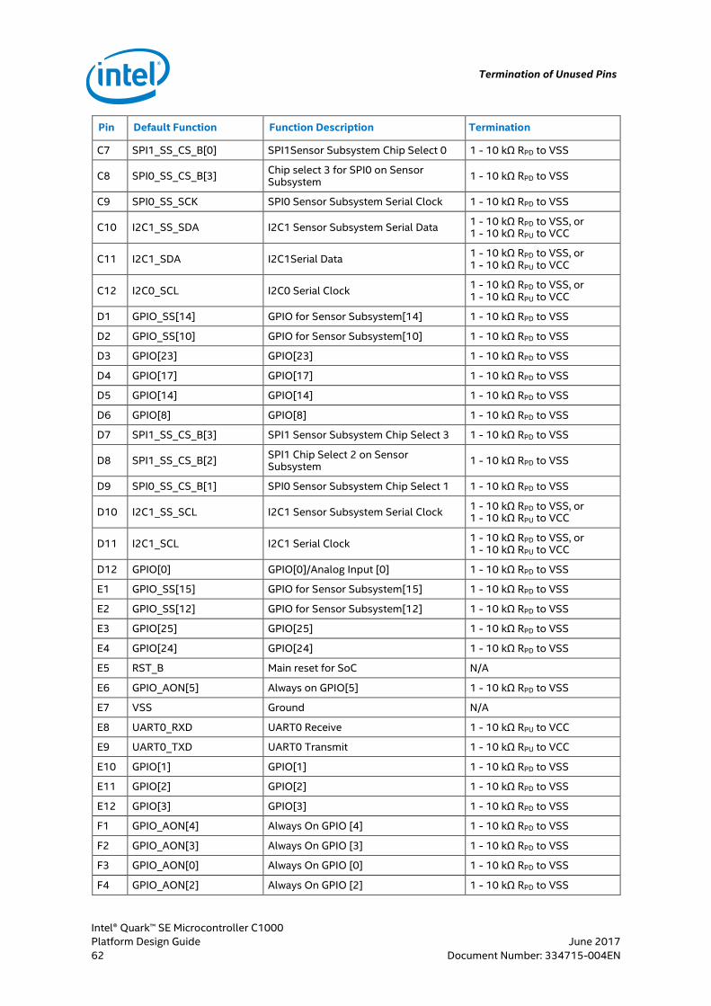
Termination of Unused Pins
Intel® Quark™ SE Microcontroller C1000
Platform Design Guide June 2017
62 Document Number: 334715-004EN
Pin Default Function Function Description Termination
C7 SPI1_SS_CS_B[0] SPI1Sensor Subsystem Chip Select 0 1 - 10 kΩ RPD to VSS
C8 SPI0_SS_CS_B[3] Chip select 3 for SPI0 on Sensor Subsystem
1 - 10 kΩ RPD to VSS
C9 SPI0_SS_SCK SPI0 Sensor Subsystem Serial Clock 1 - 10 kΩ RPD to VSS
C10 I2C1_SS_SDA I2C1 Sensor Subsystem Serial Data 1 - 10 kΩ RPD to VSS, or 1 - 10 kΩ RPU to VCC
C11 I2C1_SDA I2C1Serial Data 1 - 10 kΩ RPD to VSS, or 1 - 10 kΩ RPU to VCC
C12 I2C0_SCL I2C0 Serial Clock 1 - 10 kΩ RPD to VSS, or 1 - 10 kΩ RPU to VCC
D1 GPIO_SS[14] GPIO for Sensor Subsystem[14] 1 - 10 kΩ RPD to VSS
D2 GPIO_SS[10] GPIO for Sensor Subsystem[10] 1 - 10 kΩ RPD to VSS
D3 GPIO[23] GPIO[23] 1 - 10 kΩ RPD to VSS
D4 GPIO[17] GPIO[17] 1 - 10 kΩ RPD to VSS
D5 GPIO[14] GPIO[14] 1 - 10 kΩ RPD to VSS
D6 GPIO[8] GPIO[8] 1 - 10 kΩ RPD to VSS
D7 SPI1_SS_CS_B[3] SPI1 Sensor Subsystem Chip Select 3 1 - 10 kΩ RPD to VSS
D8 SPI1_SS_CS_B[2] SPI1 Chip Select 2 on Sensor Subsystem
1 - 10 kΩ RPD to VSS
D9 SPI0_SS_CS_B[1] SPI0 Sensor Subsystem Chip Select 1 1 - 10 kΩ RPD to VSS
D10 I2C1_SS_SCL I2C1 Sensor Subsystem Serial Clock 1 - 10 kΩ RPD to VSS, or 1 - 10 kΩ RPU to VCC
D11 I2C1_SCL I2C1 Serial Clock 1 - 10 kΩ RPD to VSS, or 1 - 10 kΩ RPU to VCC
D12 GPIO[0] GPIO[0]/Analog Input [0] 1 - 10 kΩ RPD to VSS
E1 GPIO_SS[15] GPIO for Sensor Subsystem[15] 1 - 10 kΩ RPD to VSS
E2 GPIO_SS[12] GPIO for Sensor Subsystem[12] 1 - 10 kΩ RPD to VSS
E3 GPIO[25] GPIO[25] 1 - 10 kΩ RPD to VSS
E4 GPIO[24] GPIO[24] 1 - 10 kΩ RPD to VSS
E5 RST_B Main reset for SoC N/A
E6 GPIO_AON[5] Always on GPIO[5] 1 - 10 kΩ RPD to VSS
E7 VSS Ground N/A
E8 UART0_RXD UART0 Receive 1 - 10 kΩ RPU to VCC
E9 UART0_TXD UART0 Transmit 1 - 10 kΩ RPU to VCC
E10 GPIO[1] GPIO[1] 1 - 10 kΩ RPD to VSS
E11 GPIO[2] GPIO[2] 1 - 10 kΩ RPD to VSS
E12 GPIO[3] GPIO[3] 1 - 10 kΩ RPD to VSS
F1 GPIO_AON[4] Always On GPIO [4] 1 - 10 kΩ RPD to VSS
F2 GPIO_AON[3] Always On GPIO [3] 1 - 10 kΩ RPD to VSS
F3 GPIO_AON[0] Always On GPIO [0] 1 - 10 kΩ RPD to VSS
F4 GPIO_AON[2] Always On GPIO [2] 1 - 10 kΩ RPD to VSS
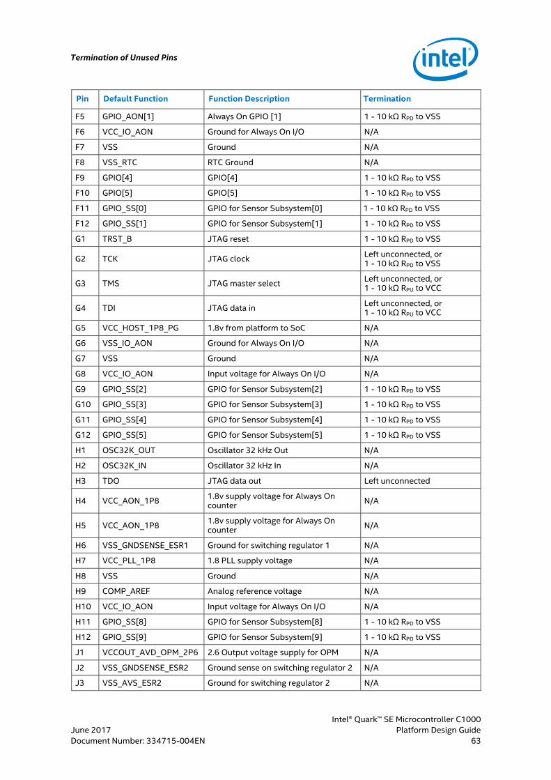
Termination of Unused Pins
Intel® Quark™ SE Microcontroller C1000
June 2017 Platform Design Guide
Document Number: 334715-004EN 63
Pin Default Function Function Description Termination
F5 GPIO_AON[1] Always On GPIO [1] 1 - 10 kΩ RPD to VSS
F6 VCC_IO_AON Ground for Always On I/O N/A
F7 VSS Ground N/A
F8 VSS_RTC RTC Ground N/A
F9 GPIO[4] GPIO[4] 1 - 10 kΩ RPD to VSS
F10 GPIO[5] GPIO[5] 1 - 10 kΩ RPD to VSS
F11 GPIO_SS[0] GPIO for Sensor Subsystem[0] 1 - 10 kΩ RPD to VSS
F12 GPIO_SS[1] GPIO for Sensor Subsystem[1] 1 - 10 kΩ RPD to VSS
G1 TRST_B JTAG reset 1 - 10 kΩ RPD to VSS
G2 TCK JTAG clock Left unconnected, or 1 - 10 kΩ RPD to VSS
G3 TMS JTAG master select Left unconnected, or 1 - 10 kΩ RPU to VCC
G4 TDI JTAG data in Left unconnected, or 1 - 10 kΩ RPU to VCC
G5 VCC_HOST_1P8_PG 1.8v from platform to SoC N/A
G6 VSS_IO_AON Ground for Always On I/O N/A
G7 VSS Ground N/A
G8 VCC_IO_AON Input voltage for Always On I/O N/A
G9 GPIO_SS[2] GPIO for Sensor Subsystem[2] 1 - 10 kΩ RPD to VSS
G10 GPIO_SS[3] GPIO for Sensor Subsystem[3] 1 - 10 kΩ RPD to VSS
G11 GPIO_SS[4] GPIO for Sensor Subsystem[4] 1 - 10 kΩ RPD to VSS
G12 GPIO_SS[5] GPIO for Sensor Subsystem[5] 1 - 10 kΩ RPD to VSS
H1 OSC32K_OUT Oscillator 32 kHz Out N/A
H2 OSC32K_IN Oscillator 32 kHz In N/A
H3 TDO JTAG data out Left unconnected
H4 VCC_AON_1P8 1.8v supply voltage for Always On counter
N/A
H5 VCC_AON_1P8 1.8v supply voltage for Always On counter
N/A
H6 VSS_GNDSENSE_ESR1 Ground for switching regulator 1 N/A
H7 VCC_PLL_1P8 1.8 PLL supply voltage N/A
H8 VSS Ground N/A
H9 COMP_AREF Analog reference voltage N/A
H10 VCC_IO_AON Input voltage for Always On I/O N/A
H11 GPIO_SS[8] GPIO for Sensor Subsystem[8] 1 - 10 kΩ RPD to VSS
H12 GPIO_SS[9] GPIO for Sensor Subsystem[9] 1 - 10 kΩ RPD to VSS
J1 VCCOUT_AVD_OPM_2P6 2.6 Output voltage supply for OPM N/A
J2 VSS_GNDSENSE_ESR2 Ground sense on switching regulator 2 N/A
J3 VSS_AVS_ESR2 Ground for switching regulator 2 N/A
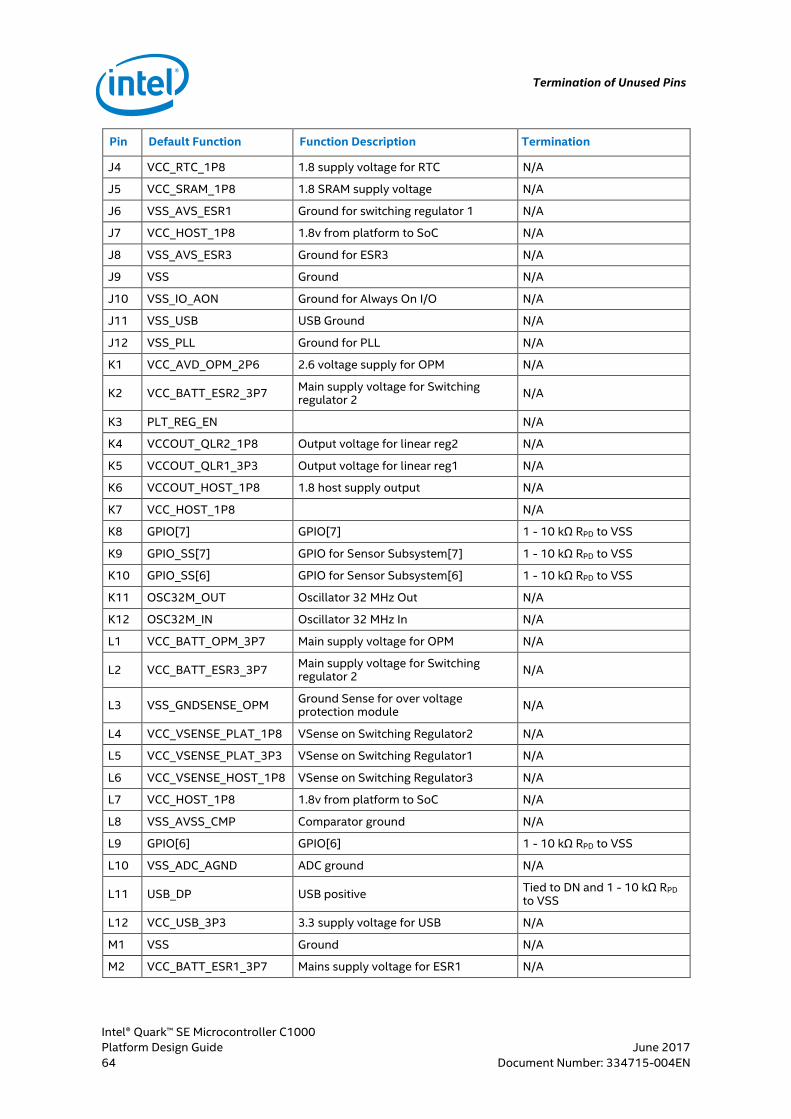
Termination of Unused Pins
Intel® Quark™ SE Microcontroller C1000
Platform Design Guide June 2017
64 Document Number: 334715-004EN
Pin Default Function Function Description Termination
J4 VCC_RTC_1P8 1.8 supply voltage for RTC N/A
J5 VCC_SRAM_1P8 1.8 SRAM supply voltage N/A
J6 VSS_AVS_ESR1 Ground for switching regulator 1 N/A
J7 VCC_HOST_1P8 1.8v from platform to SoC N/A
J8 VSS_AVS_ESR3 Ground for ESR3 N/A
J9 VSS Ground N/A
J10 VSS_IO_AON Ground for Always On I/O N/A
J11 VSS_USB USB Ground N/A
J12 VSS_PLL Ground for PLL N/A
K1 VCC_AVD_OPM_2P6 2.6 voltage supply for OPM N/A
K2 VCC_BATT_ESR2_3P7 Main supply voltage for Switching regulator 2
N/A
K3 PLT_REG_EN N/A
K4 VCCOUT_QLR2_1P8 Output voltage for linear reg2 N/A
K5 VCCOUT_QLR1_3P3 Output voltage for linear reg1 N/A
K6 VCCOUT_HOST_1P8 1.8 host supply output N/A
K7 VCC_HOST_1P8 N/A
K8 GPIO[7] GPIO[7] 1 - 10 kΩ RPD to VSS
K9 GPIO_SS[7] GPIO for Sensor Subsystem[7] 1 - 10 kΩ RPD to VSS
K10 GPIO_SS[6] GPIO for Sensor Subsystem[6] 1 - 10 kΩ RPD to VSS
K11 OSC32M_OUT Oscillator 32 MHz Out N/A
K12 OSC32M_IN Oscillator 32 MHz In N/A
L1 VCC_BATT_OPM_3P7 Main supply voltage for OPM N/A
L2 VCC_BATT_ESR3_3P7 Main supply voltage for Switching regulator 2
N/A
L3 VSS_GNDSENSE_OPM Ground Sense for over voltage protection module
N/A
L4 VCC_VSENSE_PLAT_1P8 VSense on Switching Regulator2 N/A
L5 VCC_VSENSE_PLAT_3P3 VSense on Switching Regulator1 N/A
L6 VCC_VSENSE_HOST_1P8 VSense on Switching Regulator3 N/A
L7 VCC_HOST_1P8 1.8v from platform to SoC N/A
L8 VSS_AVSS_CMP Comparator ground N/A
L9 GPIO[6] GPIO[6] 1 - 10 kΩ RPD to VSS
L10 VSS_ADC_AGND ADC ground N/A
L11 USB_DP USB positive Tied to DN and 1 - 10 kΩ RPD to VSS
L12 VCC_USB_3P3 3.3 supply voltage for USB N/A
M1 VSS Ground N/A
M2 VCC_BATT_ESR1_3P7 Mains supply voltage for ESR1 N/A
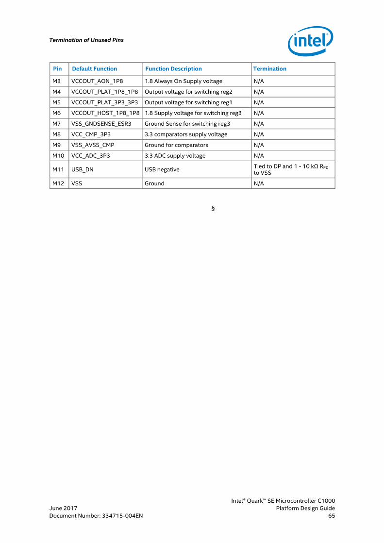
Termination of Unused Pins
Intel® Quark™ SE Microcontroller C1000
June 2017 Platform Design Guide
Document Number: 334715-004EN 65
Pin Default Function Function Description Termination
M3 VCCOUT_AON_1P8 1.8 Always On Supply voltage N/A
M4 VCCOUT_PLAT_1P8_1P8 Output voltage for switching reg2 N/A
M5 VCCOUT_PLAT_3P3_3P3 Output voltage for switching reg1 N/A
M6 VCCOUT_HOST_1P8_1P8 1.8 Supply voltage for switching reg3 N/A
M7 VSS_GNDSENSE_ESR3 Ground Sense for switching reg3 N/A
M8 VCC_CMP_3P3 3.3 comparators supply voltage N/A
M9 VSS_AVSS_CMP Ground for comparators N/A
M10 VCC_ADC_3P3 3.3 ADC supply voltage N/A
M11 USB_DN USB negative Tied to DP and 1 - 10 kΩ RPD to VSS
M12 VSS Ground N/A
§