intel® stratix® 10 mx fpga development kit user guide · • power — pcie input power including...
TRANSCRIPT

Intel® Stratix® 10 MX FPGADevelopment Kit User Guide
SubscribeSend Feedback
UG-20151 | 2019.11.29Latest document on the web: PDF | HTML

Contents
1. Overview........................................................................................................................ 41.1. General Development Kit Description........................................................................51.2. Recommended Operating Conditions........................................................................ 71.3. Handling the Development Kit................................................................................. 7
2. Getting Started............................................................................................................... 82.1. About the Intel Quartus® Prime Software..................................................................82.2. Development Kit Package....................................................................................... 82.3. Installing the Intel FPGA Download Cable Driver........................................................ 9
3. Development Kit Setup................................................................................................. 113.1. Applying Power to the Development Kit...................................................................113.2. Default Switch and Jumper Settings....................................................................... 12
4. Development Kit Components....................................................................................... 144.1. Components Overview..........................................................................................154.2. Intel MAX 10 FPGA System Controller..................................................................... 184.3. Intel MAX 10 FPGA Power Manager.........................................................................224.4. FPGA Configuration.............................................................................................. 264.5. Status and User I/O Elements................................................................................294.6. Interfaces and Ports............................................................................................. 30
4.6.1. PCI Express.............................................................................................304.6.2. Memory Interface.................................................................................... 354.6.3. High Bandwidth Memory (HBM2)................................................................494.6.4. QSFP......................................................................................................514.6.5. I2C.........................................................................................................534.6.6. Flash Memory..........................................................................................55
4.7. HiLo Daughter Cards............................................................................................ 564.7.1. DDR4..................................................................................................... 574.7.2. QDR-IV...................................................................................................57
4.8. Clocks................................................................................................................ 594.9. Power.................................................................................................................60
4.9.1. Power Guidelines..................................................................................... 614.9.2. Power Distribution System........................................................................ 624.9.3. Power Sequence...................................................................................... 634.9.4. Power Measurement................................................................................. 644.9.5. Power Fast Discharging.............................................................................644.9.6. Thermal Limitations and Protection.............................................................654.9.7. Cooling Design........................................................................................ 654.9.8. Mechanical Information.............................................................................664.9.9. Top Cover Removal.................................................................................. 67
5. Board Test System........................................................................................................ 695.1. Preparing the Board............................................................................................. 705.2. Running the Board Test System............................................................................. 70
Before you begin...............................................................................................71To run the BTS..................................................................................................71
5.3. Using the Board Test System................................................................................. 71
Contents
Intel® Stratix® 10 MX FPGA Development Kit User Guide Send Feedback
2

5.3.1. The Configure Menu................................................................................. 715.3.2. The Sys Info Tab......................................................................................725.3.3. The QSFP Tab..........................................................................................735.3.4. The PCIE Tab...........................................................................................765.3.5. The Component DDR4 Tab.........................................................................805.3.6. The HiLo DDR4 Tab.................................................................................. 815.3.7. The DDR4 Dimm Tab................................................................................ 835.3.8. The HBM2 Top Tab................................................................................... 845.3.9. The HBM2 Bottom Tab.............................................................................. 855.3.10. Power Monitor........................................................................................865.3.11. Clock Controller..................................................................................... 88
A. Additional Information................................................................................................. 91A.1. Add SmartVID settings in the QSF file.................................................................... 91A.2. Safety and Regulatory Information.........................................................................92
A.2.1. Safety Warnings...................................................................................... 92A.2.2. Safety Cautions....................................................................................... 94
A.3. Compliance and Conformity Statement................................................................... 96
B. Revision History............................................................................................................97B.1. Revision History for Intel Stratix 10 MX FPGA Development Kit User Guide.................. 97
Contents
Send Feedback Intel® Stratix® 10 MX FPGA Development Kit User Guide
3

1. OverviewThe Intel® Stratix® 10 MX FPGA development kit provides a hardware platform forevaluating the performance and features of the Intel Stratix 10 MX device.
Table 1. Ordering Information
Board Version Board Part Number Device Part Number
Intel Stratix 10 MX FPGA H-Tile (8 GB) DK-DEV-1SMX-H-A 1SM21BHU2F53E1VG
Intel Stratix 10 MX FPGA H-Tile (16 GB) DK-DEV-1SMC-H-A 1SM21CHU1F53E1VG
UG-20151 | 2019.11.29
Send Feedback
Intel Corporation. All rights reserved. Agilex, Altera, Arria, Cyclone, Enpirion, Intel, the Intel logo, MAX, Nios,Quartus and Stratix words and logos are trademarks of Intel Corporation or its subsidiaries in the U.S. and/orother countries. Intel warrants performance of its FPGA and semiconductor products to current specifications inaccordance with Intel's standard warranty, but reserves the right to make changes to any products and servicesat any time without notice. Intel assumes no responsibility or liability arising out of the application or use of anyinformation, product, or service described herein except as expressly agreed to in writing by Intel. Intelcustomers are advised to obtain the latest version of device specifications before relying on any publishedinformation and before placing orders for products or services.*Other names and brands may be claimed as the property of others.
ISO9001:2015Registered

1.1. General Development Kit Description
Figure 1. Intel Stratix 10 MX FPGA Development Kit Block Diagram
4N4M
Top HBM2
Bot HBM2 S10 MX
4L
TransceiversPcie Hard IP (CvP)
TransceiversPcie Hard IP
4K4F4E4D4C
1N1M1L1K1F1E1D1C
3I
3J
3K
3L
2K
2N
2L
2M
2N
3C
JTAG
IOs
JTAG
Supports DDR4/QDR-IV
AS x4Fast Mode
Other JTAGs
3B
3A
SDM
2F
2C
2B
2A
Config QSPI2Gb Flash
MAX 10USB
BLASTERJTAG SWI2C CTRL
HiLo Conn
USBPHYUSB
I2C I2CCh0, Ch1, Ch3, Ch4Map to 100G HIP
Ch0, Ch1, Ch3, Ch4Map to 100G HIP
MT40A512M16 x5
GPIOs, Push- bottons, LEDs
+12V for DDR-T Support
8GB ECC
I2C
I2C
PCle Gen3 x16 Root Port QSFP28-2
PCle Gen3 x16 End Point QSFP28-1
JTAG HDRDIMM
DDR4/DDR-T
Voltage SenseInputs
CurrentSenseInputs
Seq Ctrl
TempDiodes
+12V from PCleGold Fingers
Aux 12V ConnAll Clocks
All Voltages
PowerRegulators &
Discharge CKT
MAX 10Power Seq.
Power Monitor
Hot-plug &PWR or CKT
Clocks
TempSense
CurrentSense
Aux12V
x16
25Gx
4
x16
25Gx
4
x72
x72
x72
DDR410Gb x5
1. Overview
UG-20151 | 2019.11.29
Send Feedback Intel® Stratix® 10 MX FPGA Development Kit User Guide
5

Feature Summary
• Intel Stratix 10 MX FPGA device
— 0.85 V - 0.89 V VID-adjustable VCC core, 1 mm pitch, 2597 pin BGA
— H-Tile transceivers capable of 28.3 gigabit per second (Gbps) data rates
— HBM2 embedded memory tiles: 8 GB (4 GB x 2) or 16 GB (8 GB x 2)
• FPGA Configuration
— Partial reconfiguration support
— 2 gigabits (Gb) QSPI Flash
— Storage for two configuration images in flash (Factory and User)
— JTAG header for device programming
— Built-in Intel FPGA Download Cable II for device programming
• Programmable Clock Sources
— 644.53125 MHz Differential LVDS for QSFP
— 100.000 MHz Differential LVDS for PCIe*
— 133.333 MHz Differential LVDS to Memory
— 125 MHz Configuration Clock
• Transceiver Interfaces
— PCIe x16 interface supporting Gen3 End-Point mode connected to a x16 PCIeedge connector (gold edge fingers)
— PCIe x16 interface supporting Gen3 Root-Port mode connected to a x16straddle-mount PCIe edge connector
— 2x standard QSFP28 optical module interfaces connected to the FPGA H-Tiletransceivers
• Memory Interfaces
— One on-board independent single rank DDR4 x72 (ECC) channels operating at1333 MHz (DDR4-2666)
— One DIMM socket supporting DDR4 DIMM or DDR-T DIMM
— One HiLo connector supporting DDR4 and QDR-IV
• Communication Ports
— 2x QSFP28 optical interface port
— JTAG header
— USB (Micro) on-board Intel FPGA Download Cable II
• Buttons, Switches and LEDs
— System Reset Pushbutton
— CPU Reset Pushbutton
— PCIe Reset Pushbutton
— Four dedicated User LEDs
— Two dedicated configuration status LEDs
1. Overview
UG-20151 | 2019.11.29
Intel® Stratix® 10 MX FPGA Development Kit User Guide Send Feedback
6

• Heatsink and Fan
— Air-cooled heatsink assembly
— Red Over-Temperature Warning LED Indicator
• Power
— PCIe input power including required 2 x 4 Aux power connector
— Blue Power-On LED
— On/Off Slide Power Switch for bench-top operation
— On board Power Measurement Circuitry
• Mechanical
— PCIe standard height form factor
— 4.376” x 10.8” board size
— 3 Slots height requirement (with Air-cooled thermal solution)
• Operating Environment
— Maximum ambient temperature of 0 °C - 35 °C
1.2. Recommended Operating Conditions
• Recommended ambient operating temperature range: 0 °C to 35 °C
• Maximum ICC load current: 192 A
• Maximum ICC load transient percentage: 30 %
• Maximum board power consumption: 192 Watts
1.3. Handling the Development Kit
When handling the kit, it is important to observe static discharge precautions.
Note: Without proper anti-static handling, the board could be damaged. Use anti-statichandling precautions when handling the board.
Note: You must not operate this development kit in a Vibration environment.
Note: This development kit requires the top cover to be enclosed for proper cooling duringoperation.
1. Overview
UG-20151 | 2019.11.29
Send Feedback Intel® Stratix® 10 MX FPGA Development Kit User Guide
7

2. Getting Started
2.1. About the Intel Quartus® Prime Software
The Intel Quartus® Prime design software is a multi-platform design environment thateasily adapts to your specific needs in all phases of FPGA, CPLD and SoC designs. TheIntel Quartus Prime software delivers the highest performance and productivity forIntel FPGAs, CPLDs, and SoCs.
The Intel Quartus Prime Design Suite software includes everything needed to designfor using Intel FPGAs, SoCs and CPLDs from design entry and synthesis tooptimization, verification and simulation.
Intel Quartus Prime Software
The Intel Quartus Prime Design Suite software is available in three editions based onspecific design requirements: Pro, Standard, and Lite Edition.
The Intel Quartus Prime Pro Edition is optimized to support the advanced features inIntel's next generation FPGAs and SoCs.
The Intel Stratix 10 MX FPGA is only supported on Intel Quartus Prime Pro Edition.There is no paid license fee required for Intel Stratix 10 support in Intel Quartus PrimePro Edition.
Included in the Intel Quartus Prime Pro Edition are the Intel Quartus Prime software,Nios® II EDS and the Intel FPGA IP Library.
To install Intel's development tools, download the Intel Quartus Prime Pro Editionsoftware from the Quartus Prime Pro Edition page from the Download Center of Intel'swebsite.
2.2. Development Kit Package
To download the Intel Stratix 10 MX FPGA Development Kit package, perform thefollowing steps:
1. Download the development kit package from the Intel Stratix 10 MX FPGADevelopment Kit link (provided below) on the Intel website.
2. Unzip the Intel Stratix 10 MX FPGA Development Kit package contents to yourmachine's local hard drive.
3. The package creates the directory structure shown in the figure below.
UG-20151 | 2019.11.29
Send Feedback
Intel Corporation. All rights reserved. Agilex, Altera, Arria, Cyclone, Enpirion, Intel, the Intel logo, MAX, Nios,Quartus and Stratix words and logos are trademarks of Intel Corporation or its subsidiaries in the U.S. and/orother countries. Intel warrants performance of its FPGA and semiconductor products to current specifications inaccordance with Intel's standard warranty, but reserves the right to make changes to any products and servicesat any time without notice. Intel assumes no responsibility or liability arising out of the application or use of anyinformation, product, or service described herein except as expressly agreed to in writing by Intel. Intelcustomers are advised to obtain the latest version of device specifications before relying on any publishedinformation and before placing orders for products or services.*Other names and brands may be claimed as the property of others.
ISO9001:2015Registered

Figure 2. Development Kit Directory Structure
<package rootdir>
board design files
demos
documents
examples
factory recovery
The table below lists the file directory names and a description of their contents
Table 2. Installed Development Kit Directory Structure
Directory Name Description of Directory Contents
board_design_files Contains schematics, layout, assembly and bill of materialboard design files. Use these files as a starting point for anew prototype board design
demos Contains demonstration applications when available
documents Contains the development kit documentation
examples Contains the sample design files for the development kit
factory_recovery Contains the original data programmed onto the boardbefore shipment. Use this data to restore the board with itsoriginal factory contents.
Note: To view the layout *.brd files in the board package, you can download the Cadence®
Allegro®/OrCAD® Free Viewer from Cadence's website.
Related Information
• Intel Stratix 10 MX FPGA Development KitThe downloadable development kit package is in Table #3 at the link providedon Intel website.
• Cadence Allegro Downloads
2.3. Installing the Intel FPGA Download Cable Driver
The Intel Stratix 10 MX FPGA Development Kit includes embedded Intel FPGADownload Cable circuits for FPGA programming. However, for the host computer andboard to communicate, you must install the Intel FPGA Download Cable driver on thehost computer.
Installation instructions for the Intel FPGA Download Cable driver for your operatingsystem are available on the Intel website.
2. Getting Started
UG-20151 | 2019.11.29
Send Feedback Intel® Stratix® 10 MX FPGA Development Kit User Guide
9

On the Intel website, navigate to the Cable and Adapter Drivers Information link tolocate the table entry for your configuration and click the link to access theinstructions.
2. Getting Started
UG-20151 | 2019.11.29
Intel® Stratix® 10 MX FPGA Development Kit User Guide Send Feedback
10

3. Development Kit SetupThis chapter describes how to apply power to the development board and providesdefault switch and jumper settings.
3.1. Applying Power to the Development Kit
This development kit is designed to operate in two modes:
As a PCIe add-in card
When operating the card as a PCIe system, insert the card into an available PCIe slotand connect a 2x4 pin PCIe power cable from the system to the power connectors atAux power connector J11 of the board.
Note: When operating as a PCIe add-in card, the board does not power on unless power issupplied to J11.
In bench-top mode
In bench-top mode, you must supply the board with the provided 240 W power supplyconnected to the Aux power connector J11, as follows
Note: This development board ships with its switches preconfigured to support the designexamples in the kit. If you suspect that your board may not be correctly configuredwith the default settings, follow the instructions in the Default Switch and JumperSettings on page 12 of this chapter.
1. Connect the provided power supply to an outlet and the DC Power Jack (J11) onthe FPGA board.
Note: Use only the supplied power supply. Power regulation circuits on the boardcan be damaged by power supplies with greater voltage.
2. Set the power switch (SW3) to the ON position.
When the board powers up, the blue power LED illuminates and the board is ready foruse.
UG-20151 | 2019.11.29
Send Feedback
Intel Corporation. All rights reserved. Agilex, Altera, Arria, Cyclone, Enpirion, Intel, the Intel logo, MAX, Nios,Quartus and Stratix words and logos are trademarks of Intel Corporation or its subsidiaries in the U.S. and/orother countries. Intel warrants performance of its FPGA and semiconductor products to current specifications inaccordance with Intel's standard warranty, but reserves the right to make changes to any products and servicesat any time without notice. Intel assumes no responsibility or liability arising out of the application or use of anyinformation, product, or service described herein except as expressly agreed to in writing by Intel. Intelcustomers are advised to obtain the latest version of device specifications before relying on any publishedinformation and before placing orders for products or services.*Other names and brands may be claimed as the property of others.
ISO9001:2015Registered

3.2. Default Switch and Jumper Settings
Figure 3. Default Switch Settings
3. Development Kit Setup
UG-20151 | 2019.11.29
Intel® Stratix® 10 MX FPGA Development Kit User Guide Send Feedback
12

Table 3. SW2 DIP JTAG Switch Default Settings (Board Bottom)
Switch Board Label Function Default Position
1 JTAG INPUT JTAG Source Select OFF (On-board Intel FPGADownload Cable)
2 M10 Intel MAX® 10 JTAG ON (JTAG OUT)
3 PCIE RT PCIe Root Port JTAG ON (JTAG OUT)
4 S10 Intel Stratix 10 FPGA JTAG OFF (JTAG IN)
Table 4. SW1 DIP PMBus Switch Default Settings (Board Bottom)
Switch Board Label Function Default Position
1 SI5341 I2C BUS Clock Generator I2C Bus OFF (Enable)
2 3V3 I2C BUS 3V3 VRM I2C BUS OFF (Enable)
3 MAIN I2C BUS MAIN I2C BUS OFF (Enable)
4 S10 PMBus Intel Stratix 10 FPGA PMBus OFF (Enable)
3. Development Kit Setup
UG-20151 | 2019.11.29
Send Feedback Intel® Stratix® 10 MX FPGA Development Kit User Guide
13

4. Development Kit ComponentsThis chapter introduces all the important components on the development kit. Acomplete set of schematics, a physical layout database and Gerber files for thedevelopment board reside in the development kit documents directory.
Figure 4. Intel Stratix 10 MX FPGA Development Kit - Front
Figure 5. Intel Stratix 10 MX FPGA Development Kit - Rear
UG-20151 | 2019.11.29
Send Feedback
Intel Corporation. All rights reserved. Agilex, Altera, Arria, Cyclone, Enpirion, Intel, the Intel logo, MAX, Nios,Quartus and Stratix words and logos are trademarks of Intel Corporation or its subsidiaries in the U.S. and/orother countries. Intel warrants performance of its FPGA and semiconductor products to current specifications inaccordance with Intel's standard warranty, but reserves the right to make changes to any products and servicesat any time without notice. Intel assumes no responsibility or liability arising out of the application or use of anyinformation, product, or service described herein except as expressly agreed to in writing by Intel. Intelcustomers are advised to obtain the latest version of device specifications before relying on any publishedinformation and before placing orders for products or services.*Other names and brands may be claimed as the property of others.
ISO9001:2015Registered

Figure 6. Intel Stratix 10 MX FPGA Development Kit Picture
LT PMBus Connector (J13)
Ext. JTAGConnector (J9)S10 PCle
PERST 0 (S1)
S10 PCle PERST 1 (S11)
USB Connector (J15)
QSFP 2 (J4)
HILO Connector (J2)PCle X16 End Point
Edge Connector (J6)
MAX10 Reset (S12)
QSFP 1 (J5)
PCle Root Port Connector (J7)
DIMM Socket (J1)ATX Aux
Connector (J11)
Power LED (D4)
OverTemp LED (D5)
Power Switch (SW3)
User LED 0 (D7)User LED 1 (D8)User LED 2 (D9)
User LED 3 (D10)CPU Reset (S10)S10 Config_Done LED (S14)
S10 CvP_Done LED (D16)
Fan Connector LED (J10)
RZQ Jumper (J3) Enpirion PMBusConnector (J12)
4.1. Components Overview
Table 5. Development Kit Components Table
Board Reference Type Description
Featured Devices
U1 FPGA Intel Stratix 10 MX FPGA(1)
• Adaptive Logic Modules (ALM):702,720
• Logic Elements (LE): 2,073K• Registers: 2,810,880• M20K Memory Blocks: 6,847• Transceiver Count: 96• Package Type: 2597 BGA• HMB2 DRAM (GB): 8 or 16
U11 FPGA Intel MAX 10 FPGA, 4K LEs, 169 FBGA(System)
U27 FPGA Intel MAX 10, 16K LEs, 169 FBGA(Power)
Configuration and Setup Elements
J15 On-board Intel FPGA Download CableII
Micro-USB 2.0 connector forprogramming and debugging the FPGA.
SW2 JTAG Bypass DIP Switch Enable and disable devices in the JTAGchain. This switch is located on theback of the board.
continued...
(1) Refer to Overview on page 4 for the part number for your specific board
4. Development Kit Components
UG-20151 | 2019.11.29
Send Feedback Intel® Stratix® 10 MX FPGA Development Kit User Guide
15

Board Reference Type Description
SW1 I2C Bus Selection Switch Enable or Disable the I2C Bus for Clockchip, 3.3 V VRM, Main I2C, and IntelStratix 10 FPGA
S10 CPU reset push button The default reset for the FPGA logic.
S1 PCIe PERST 0 push button This push button connects to IntelStratix 10 FPGA's NPERSTL0 pin.
S11 PCIe PERST 1 push button This push button connects to IntelStratix 10 FPGA's NPERSTR1 pin.
S12 Intel MAX 10 Reset Push Button The default reset for the Intel MAX 10FPGA System Controller
Status Elements
D14 Configuration Done LED Illuminates when FPGA configuration iscompleted
D16 CvP Done LED Illuminates when CvP process iscompleted
D4 Power LED (Blue) Illuminates when board is powered on.
D5 Temperature LED (Green) Illuminates when an over temperaturecondition occurs for the FPGA device.Ensure that an adequate heatsink/fanis properly installed.
D7, D8, D9, D10 User-defined LEDs Four green color user LEDs. Illuminatewhen driven low.
Clock Circuits
U17 Intel MAX 10 Reference Clock Si510 Crystal Oscillator providesreference clocks for Intel MAX 10devicesDefault Frequencies are:• Out0= 50.00 MHz• Out1= 50.00 MHz
U16 Programmable Clock Generator Si5341A Programmable ClockGenerator by the clock control GUIDefault Frequencies are:• Out0= 644.53125 MHz• Out1= 644.53125 MHz• Out2= 100 MHz• Out3= 100 MHz• Out4= 100 MHz• Out5= 100 MHz• Out6= 100 MHz• Out7= 100 MHz• Out8= 100 MHz• Out9= 100 MHz
U18 Programmable Clock Generator Si5338A Programmable ClockGenerator by the Clock Control GUIDefault Frequencies are:• CLK0= 50 MHz• CLK1= 100 MHz• CLK2= 125 MHz• CLK3= 100 MHz
continued...
4. Development Kit Components
UG-20151 | 2019.11.29
Intel® Stratix® 10 MX FPGA Development Kit User Guide Send Feedback
16

Board Reference Type Description
U19 Programmable Clock Generator Si5338B Programmable ClockGenerator by the Clock Control GUIDefault Frequencies are:• CLK0= 133.333 MHz• CLK1= 133.333 MHz• CLK2= 133.333 MHz• CLK3= Not Used
Transceiver Interfaces
J6 PCIe x16 gold fingers PCIe TX/RX x16 interface from FPGAbank 1C, 1D, 1E
J7 PCIe x16 Root Port Connector PCIe TX/RX x16 interface from FPGAbank 4C, 4D, 4E
J4 QSFP Connector Four TX/RX channels from FPGA Bank1F
J5 QSFP Connector Four TX/RX channels from 4F fromFPGA bank 4F
General User Input/Output
D7, D8, D9. D10 User defined LEDs Four green color user LEDs. Illuminateswhen driven low.
Memory Devices
J2 HiLo Connector One x72 memory interface supportingDDR3 (x72), DDR4 (x72), QDR-IV(x36) and RLDRAM3 (x36).This development kit includes oneplugin modules (daughtercards) thatuse the HiLo connector: DDR4 memory(x72) 1333 MHz
J1 DDR4, DDR-T, DIMM Socket One X72 memory interface supportingDDR4 (x72) or DDR-T memory module.• DDR4 memory (x72) 1333 MHz• DDR-T memory (requires DDR-T IP)
U3, U4, U5, U6, U7 On-board DDR4 memory On-board DDR4 memory (x72) 1333MHz
Communication Ports
J6 PCI Express* x16 Edge Connector Gold-plated edge fingers for up to x16signaling in either Gen1, Gen2 or Gen3mode.
J7 PCI Express x16 Root Port Connector Standard PCI Express Gen3 x16Connector for connecting PCIeEndpoint card.
J4 QSFP interface Provides four transceiver channels perport for a 100G QSFP module
J5 QSFP interface Provides four transceiver channels perport for a 100G QSFP module
J13 Linear Tech VRM PMBus Port Provides PMBus connection usingdongle from Linear Tech.
J12 Enpirion VRM PMBus Port Provides PMBus connection usingdongle from Intel Enpirion®
continued...
4. Development Kit Components
UG-20151 | 2019.11.29
Send Feedback Intel® Stratix® 10 MX FPGA Development Kit User Guide
17

Board Reference Type Description
J9 External JTAG Port This port allows the use of Intel FPGADownload Cable II dongle to access theJTAG links on the board. Connection tothis port automatically disable theinternal Intel FPGA Download Cable IIJTAG.
J15 Micro-USB Connector Embedded Intel FPGA Download CableII JTAG for programming the FPGA viaa USB cable.
Power Supply
J6 PCI Express edge connector Interfaces to a PCI Express root portsuch as an appropriate PCmotherboard.
J11 DC Input Jack Accepts a 12 V DC power supply whenpowering the board from the providedpower brick for lab bench operation.When operating from the PCIe slot,this input must also be connected tothe 8-pin Aux PCIe power connectorprovided by the PC system along withJ11, or else the board does not poweron.
SW3 Power Switch Switch to power ON or OFF the boardwhen supplied from the DC input jack.
Related Information
Overview on page 4
4.2. Intel MAX 10 FPGA System Controller
This development kit utilizes the Intel MAX 10 FPGA (10M04SCU169) as systemcontroller for the following purposes:
• On-board Intel FPGA Download Cable
• JTAG Switch
• I2C Bus Control
• Control registers for all programmable clocks
• Control registers for QSFP and PCIe interfaces
Table 6. Intel MAX 10 FPGA System Controller Device Pin Table
Schematic Signal Name Pin Number I/O Standard Description
FX2_PA0 K6 3.3V Intel MAX 10 to USB PHYDownload Cable bus A
FX2_PA1 M4 3.3V Intel MAX 10 to USB PHYDownload Cable bus A
FX2_PA2 M5 3.3V Intel MAX 10 to USB PHYDownload Cable bus A
FX2_PA3 K5 3.3V Intel MAX 10 to USB PHYDownload Cable bus A
continued...
4. Development Kit Components
UG-20151 | 2019.11.29
Intel® Stratix® 10 MX FPGA Development Kit User Guide Send Feedback
18

Schematic Signal Name Pin Number I/O Standard Description
FX2_PA4 L4 3.3V Intel MAX 10 to USB PHYDownload Cable bus A
FX2_PA5 J5 3.3V Intel MAX 10 to USB PHYDownload Cable bus A
FX2_PA6 N4 3.3V Intel MAX 10 to USB PHYDownload Cable bus A
FX2_PA7 J7 3.3V Intel MAX 10 to USB PHYDownload Cable bus A
FX2_PB0 K7 3.3V Intel MAX 10 to USB PHYDownload Cable bus B
FX2_PB1 N9 3.3V Intel MAX 10 to USB PHYDownload Cable bus B
FX2_PB2 N7 3.3V Intel MAX 10 to USB PHYDownload Cable bus B
FX2_PB3 N6 3.3V Intel MAX 10 to USB PHYDownload Cable bus B
FX2_PB4 M13 3.3V Intel MAX 10 to USB PHYDownload Cable bus B
FX2_PB5 N5 3.3V Intel MAX 10 to USB PHYDownload Cable bus B
FX2_PB6 M9 3.3V Intel MAX 10 to USB PHYDownload Cable bus B
FX2_PB7 M11 3.3V Intel MAX 10 to USB PHYDownload Cable bus B
USB_MAX_TCK G2 3.3V Intel MAX 10 JTAG to USBPHY FX2_PD0
USB_MAX_TMS G1 3.3V Intel MAX 10 JTAG to USBPHY FX2_PD1
USB_MAX_TDI F5 3.3V Intel MAX 10 JTAG to USBPHY FX2_PD2
USB_MAX_TDO F6 3.3V Intel MAX 10 JTAG to USBPHY FX2_PD3
FX2_PD4 N8 3.3V Intel MAX 10 to USB PHYDownload Cable bus D
FX2_PD5 M7 3.3V Intel MAX 10 to USB PHYDownload Cable bus D
FX2_PD6 M8 3.3V Intel MAX 10 to USB PHYDownload Cable bus D
FX2_PD7 J6 3.3V Intel MAX 10 to USB PHYDownload Cable bus D
FX2_RESETn N3 3.3V USB PHY Reset
FX2_FLAGA J8 3.3V USB PHY FIFO output Flagsignal to Intel MAX 10
FX2_FLAGB L5 3.3V USB PHY FIFO output Flagsignal to Intel MAX 10
FX2_FLAGC L11 3.3V USB PHY FIFO output Flagsignal to Intel MAX 10
continued...
4. Development Kit Components
UG-20151 | 2019.11.29
Send Feedback Intel® Stratix® 10 MX FPGA Development Kit User Guide
19

Schematic Signal Name Pin Number I/O Standard Description
FX2_SLRDn M12 3.3V USB PHY Read signal
FX2_SLWRn N10 3.3V USB PHY Write signal
FX2_SCL K8 3.3V USB PHY I2C signal
FX2_SDA L10 3.3V USB PHY I2C signal
USB_T_CLK H6 3.3V Interface Clock from USBPHY
USB_DISABLEn N2 3.3V External JTAG signal to IntelMAX 10 for disabling internalUSB Blaster circuit
EM_PMBUS_ALERTn L1 3.3V PMBus Alert signal from IntelEnpirion Power Regulator
LT_PMBUS_ALERTn N11 3.3V PMBus Alert signal from LTPower regulator
ZQSFP0_1V8_RESET_L K10 1.8V QSFP module 0 Reset signal(Intel MAX 10 to FPGA)
ZQSFP0_1V8_MODPRS_L K11 1.8V QSFP module 0 controlsignal (Intel MAX 10 toFPGA)
ZQSFP0_1V8_LPMODE J10 1.8V QSFP module 0 Low Powersignal (Intel MAX 10 toFPGA)
ZQSFP0_1V8_INT_L L12 1.8V QSFP module 0 interruptsignal (Intel MAX 10 toFPGA)
ZQSFP0_1V8_MODSEL_L H9 1.8V QSFP module 0 Mode Selectsignal (Intel MAX 10 toFPGA)
ZQSFP1_1V8_RESET_L K12 1.8V QSFP module 1 Reset signal(Intel MAX 10 to FPGA)
ZQSFP1_1V8_MODPRS_L L13 1.8V QSFP module 1 Presentsignal (Intel MAX 10 toFPGA)
ZQSFP1_1V8_LPMODE J12 1.8V QSFP module 1 Low Powersignal (Intel MAX 10 toFPGA)
ZQSFP1_1V8_INT_L J9 1.8V QSFP module 1 interruptsignal (Intel MAX 10 toFPGA)
ZQSFP1_1V8_MODSEL_L G13 1.8V QSFP module 1 Mode Selectsignal (Intel MAX 10 toFPGA)
ZQSFP0_3V3_RESET_L B10 3.3V QSFP module 0 Reset signalto Intel MAX 10
ZQSFP0_3V3_MODPRS_L A10 3.3V QSFP module 0 controlsignal to Intel MAX 10
ZQSFP0_3V3_LPMODE A11 3.3V QSFP module 0 Low Powersignal to Intel MAX 10
continued...
4. Development Kit Components
UG-20151 | 2019.11.29
Intel® Stratix® 10 MX FPGA Development Kit User Guide Send Feedback
20

Schematic Signal Name Pin Number I/O Standard Description
ZQSFP0_3V3_INT_L E8 3.3V QSFP module 0 interruptsignal to Intel MAX 10
ZQSFP0_3V3_MODSEL_L A3 3.3V QSFP module 0 Mode Selectsignal to Intel MAX 10
ZQSFP1_3V3_RESET_L A7 3.3V QSFP module 1 Reset signalto Intel MAX 10
ZQSFP1_3V3_MODPRS_L A6 3.3V QSFP module 1 Presentsignal to Intel MAX 10
ZQSFP1_3V3_LPMODE B6 3.3V QSFP module 1 Low Powersignal to Intel MAX 10
ZQSFP1_3V3_INT_L A4 3.3V QSFP module 1 interruptsignal to Intel MAX 10
ZQSFP1_3V3_MODSEL_L B5 3.3V QSFP module 1 Mode Selectsignal to Intel MAX 10
PCIE_RT_JTAG_TCK C10 3.3V PCIe Root Port JTAG signal
PCIE_RT_JTAG_TDI A8 3.3V PCIe Root Port JTAG signal
PCIE_RT_JTAG_TMS C9 3.3V PCIe Root Port JTAG signal
PCIE_RT_JTAG_TDO A9 3.3V PCIe Root Port JTAG signal
PCIE_RT_JTAG_TRSTn B2 3.3V PCIe Root Port JTAG signal
PCIE_RT_PERSTn D1 3.3V PCIe Root Port signal
PCIE_RT_PRSNT2n C2 3.3V PCIe Rootport signal
PCIE_RT_S10_PERSTn F12 1.8V PCIe Root Port signal ( IntelMAX 10 to FPGA)
PCIE_RT_S10_PRSNT2n E12 1.8V PCIe Rootport signal ( IntelMAX 10 to FPGA)
PCIE_RT_WAKEN B4 3.3V PCIe Rootport Wake signal
PCIE_EP_JTAG_TCK E3 3.3V PCIe EndPoint JTAG signal
PCIE_EP_JTAG_TDI F1 3.3V PCIe EndPoint JTAG signal
PCIE_EP_JTAG_TMS C1 3.3V PCIe EndPoint JTAG signal
PCIE_EP_JTAG_TDO F4 3.3V PCIe EndPoint JTAG signal
S10_CVP_CONFDONE E9 1.8V CVP_CONFDONE signal fromFPGA to Intel MAX 10
S10_CONF_DONE B11 1.8V CONF_DONE signal fromFPGA to Intel MAX 10
S10_INIT_DONE C12 1.8V INIT_DONE signal fromFPGA to Intel MAX 10
CPU_RESETn C13 1.8V RESETn signal fromIntelMAX 10 to FPGA
S10_NCONFIG D9 1.8V N_CONFIG signal from IntelMAX 10 to FPGA
SI5341_ENn B13 1.8V Clock enable signal
SI5341_RSTn C11 1.8V Check chip reset
continued...
4. Development Kit Components
UG-20151 | 2019.11.29
Send Feedback Intel® Stratix® 10 MX FPGA Development Kit User Guide
21

Schematic Signal Name Pin Number I/O Standard Description
SI5341_FINC A!2 1.8V Clock Frequency incrementcontrol
SI5341_FDEC E10 1.8V Clock Frequency decrementcontrol
EXT_JTAG_TDI L3 3.3V External JTAG signal
EXT_JTAG_TCK J1 3.3V External JTAG signal
EXT_JTAG_TMS M2 3.3V External JTAG signal
EXT_JTAG_TDO K2 3.3V External JTAG signal
PWR_MAX10_BYPASSn J2 3.3V Power Intel MAX 10 JTAGBypass input (select by Dipswitch SW2-2)
PCIE_RT_BYPASSn M2 3.3V PCIe Root Port JTAG Bypassinput (select by Dip SwitchSW2-3)
S10_BYPASSn E4 3.3V FPGA JTAG Bypass input(select by Dip SwitchSW2-4)
JTAG_INPUT_SOURCE M3 3.3V JTAG input source selection,SW2-1 select betweenexternal JTAG or PCIE EPJTAG
PCIE_EP_3V3_I2C_SDA L2 3.3V I2C bus from PCIE_End Point
PCIE_EP_3V3_I2C_SCL K1 3.3V I2C bus from PCIE_End Point
MAIN_I2C_SCL F8 1.8V Main I2C bus (Intel MAX 10)
MAIN_I2C_SDA B12 1.8V Main I2C bus (Intel MAX 10)
3V3_I2C_EN H3 3.3V This Intel MAX 10 signalcontrols U22 that allows3V3_I2C bus connect to theMain I2C bus
S10_PMBUS_EN G4 3.3V This Intel MAX 10 signalcontrols U20 that allowsCORE_PMBus connect to theS10 SDM I2C bus
MAIN_PMBUS_EN H2 3.3V This Intel MAX 10 signalcontrols U21 that allowsCORE_PMBus connect toMAIN I2C bus
PWR_GOOD E1 3.3V Power Good signal from IntelMAX 10 Power
4.3. Intel MAX 10 FPGA Power Manager
This development kit utilizes the Intel MAX 10 FPGA 10M16SAU169 FPGA as PowerManager (U27) for the following purposes:
4. Development Kit Components
UG-20151 | 2019.11.29
Intel® Stratix® 10 MX FPGA Development Kit User Guide Send Feedback
22

• Power Sequencing Control
• Power Discharging Control
• Voltage Monitoring
• Fan Control
Table 7. Intel MAX 10 FPGA Power Manager Pin Table
Schematic Signal Name Pin Number I/O Standard Description
3p3V_EN L5 3.3V Enable or disable 3.3Vpower rail
S10_VCC_EN M4 3.3V Enable or disable FPGA Corepower rail
S10_VCCERAM_EN L4 3.3V Enable or disable VCCERAMpower rail
S10_VCCRL_EN M5 3.3V Enable or disable Left sideReceiver Power VCCRLpower rail
S10_VCCRR K5 3.3V Enable or disable Right sideReceiver Power VCCRRpower rail
S10_VCCT N4 3.3V Enable or disableTransmitter Power VCCTpower rail
1p8V_EN J5 3.3V Enable or disable 1.8Vpower rail
VCCIO_UIB_EN N5 3.3V Enable or disableVCCIO_UIB power rail
VCCM_EN N6 3.3V Enable or disable VCCMpower rail
1p2V_DDR4_EN N7 3.3V Enable or disable 1.2V forDDR4 power rail
HILO_VDDQ_EN M7 3.3V Enable or disable VDDQpower rail for HILO memory
HILO_VDD_EN N8 3.3V Enable or disable VDD powerrail for HILO memory
2p5V_EN J6 3.3V Enable or disable 2.5Vpower rail
ZQSFP0_PWR_EN M8 3.3V Enable or disable the powerto QSFP_0 module
ZQSFP1_PWR_EN K6 3.3V Enable or disable the powerto QSFP_1 module
DIMM_VTT_EN M9 3.3V Enable or disable thetermination power for DDR4DIMM
COMP_VTT_EN J7 3.3V Enable or disable thetermination power for on-board DDR4 memory
POWER_ON M13 3.3V Signal from power inputcircuit to Intel MAX 10 forstarting power sequencing
continued...
4. Development Kit Components
UG-20151 | 2019.11.29
Send Feedback Intel® Stratix® 10 MX FPGA Development Kit User Guide
23

Schematic Signal Name Pin Number I/O Standard Description
1p2V_DDR4_DIS N2 3.3V Signal to enable dischargecircuit for 1.2 V DDR4 powerrail
VCCIO_UIB_DIS N3 3.3V Signal to enable dischargecircuit for 1.2 V VCCIO UIBpower rail
HILO_VDD_DIS M11 3.3V Signal to enable dischargecircuit for HILO VDD powerrail
HILO_VDDQ_DIS L11 3.3V Signal to enable dischargecircuit for HILO VDDQ powerrail
VCCM_DIS K8 3.3V Signal to enable dischargecircuit for HBM's VCCMpower rail
1p8V_DIS G9 3.3V Signal to enable dischargecircuit for 1.8 V power rail
VCCRL_GXB_DIS G10 3.3V Signal to enable dischargecircuit for VCCRL_GXB powerrail
VCCRR_GXB_DIS F13 3.3V Signal to enable dischargecircuit for VCCRR_GXBpower rail
VCCT_DIS E13 3.3V Signal to enable dischargecircuit for VCCT_GXB powerrail
VCCERAM_DIS F9 3.3V Signal to enable dischargecircuit for VCCERAM powerrail
2p5V_DIS F10 3.3V Signal to enable dischargecircuit for 2.5V power rail
3p3V_DIS C10 3.3V Signal to enable dischargecircuit for 3.3V power rail
I2C_3V3_SDA M12 3.3V I2C signals
I2C_3V3_SCL N9 3.3V I2C signals
PWR_MAX10_JTAG_TMS G1 3.3V JTAG signals
PWR_MAX10_JTAG_TCK G2 3.3V JTAG signals
PWR_MAX10_JTAG_TDI F5 3.3V JTAG signals
PWR_MAX10_JTAG_TDO F6 3.3V JTAG signals
3p3V _PG A6 3.3V Power Good signal from 3.3Vpower supply
S10_VCC_PG A9 3.3V Power Good signal from VCCCore power supply
S10_VCCERAM_PG B10 3.3V Power Good signal fromVCCERAM power supply
S10_VCCRL_PG A10 3.3V Power Good signal fromVCCRL power supply
continued...
4. Development Kit Components
UG-20151 | 2019.11.29
Intel® Stratix® 10 MX FPGA Development Kit User Guide Send Feedback
24

Schematic Signal Name Pin Number I/O Standard Description
S10_VCCRR_PG A11 3.3V Power Good signal fromVCCRR power supply
S10_VCCT_PG E8 3.3V Power Good signal fromVCCT power supply
1p8V_PG A4 3.3V Power Good signal from 1.8Vpower supply
1p2V_VCCIO_UIB_PG A7 3.3V Power Good signal fromVCCIO_UIB power supply
VCCM_PG A4 3.3V Power Good signal fromVCCM power supply
HILO_VDD_PG B5 3.3V Power Good signal from VDDpower supply for HILO
HILO_VDDQ_PG A3 3.3V Power Good signal fromVDDQ power supply for HILO
1p2V_DDR4_PG E6 3.3V Power Good signal from 1.2Vpower supply for DDR4Memory
12V_G1_PG F12 3.3V Power Good signal from 12VGroup1 of input powercircuit
12V_G2_PG E12 3.3V Power Good signal from 12VGroup2 of input powercircuit
5V_PG C13 3.3V Power Good signal from 5Vpower supply
2p5V_PG E10 3.3V Power Good signal from 2.5Vpower supply
COMP_VTT_PG F8 3.3V Power Good signal from on-board DDR4 terminationpower supply
DIMM_VTT_PG B13 3.3V Power Good signal fromDIMM DDR4 terminationpower supply
12V_G1_UV_PG D9 3.3V Power Good signal from 12VGroup 1's Under-Voltagemonitor
12V_G1_OV_PG D12 3.3V Power Good signal from 12VGroup 1's Over-Voltagemonitor
S10_VCCFAULT B4 3.3V Fault signal from FPGA VCCCore power supply
EM_PMBUS_ALERTn B11 3.3V Alert signal from Enpirionpower regulators
LT_PMBUS_ALERTn C12 3.3V Alert signal from LinearTechnology power regulators
ZQSFP0_FAULT_N C11 3.3V Fault signal from QSFP_0module
ZQSFP1_FAULT_N A12 3.3V Fault signal from QSFP_1module
continued...
4. Development Kit Components
UG-20151 | 2019.11.29
Send Feedback Intel® Stratix® 10 MX FPGA Development Kit User Guide
25

Schematic Signal Name Pin Number I/O Standard Description
PCIE_RT_PRSNT2n D11 3.3V PCIE Root Port Presentsignal
PCIE_EP_PERSTN H4 3.3V PCIE End Point Presentsignal
PWR_LED_DR B12 3.3V Power LED drive signal
PWR_GOOD E9 3.3V Power Good signal of allpower supplies to Intel MAX10 System Controller
OVERTEMPn K11 3.3V Over Temperature signalfrom Board Temp sensorchip U29
TSENSE_ALERTn L12 3.3V Temperature Sense Alertsignal from Board Tempsensor chip U29
FAN_CTRL K12 3.3V Fan speed control signal tocooling fans driver
S10MX_VCC D2 Analog FPGA Core Voltage sensinginput
S10_VCCERAM D1 Analog VCCERAM Voltage sensinginput
S10_VCCRL_GXB C2 Analog FPGA Left side receivervoltage sensing input
S10_VCCRR_GXB E3 Analog FPGA Right side receivervoltage sensing input
S10_VCCT_GXB E4 Analog FPGA Transmitter voltagesensing input
1p2V_VCCIO_UIB C1 Analog 1.2V VCCIO UIB Voltagesensing input
1p8V B1 Analog 1.8V Voltage sensing input
1p2V_DDR4 F1 Analog 1,2V for DDR4 voltagesensing input
VCCM E1 Analog VCCM for HMB voltagesensing input
4.4. FPGA Configuration
You can use the Intel Quartus Prime Programmer to configure the FPGA with yourSRAM Object File (.sof).
Ensure the following
• The Intel Quartus Prime Programmer is installed on your PC.
• The micro-USB cable is connected to the FPGA development board.
• Power to the board is ON, and no other applications that use the JTAG chain arerunning.
4. Development Kit Components
UG-20151 | 2019.11.29
Intel® Stratix® 10 MX FPGA Development Kit User Guide Send Feedback
26

Steps
1. Start the Intel Quartus Prime Programmer.
2. Click Auto Detect to display the devices in the JTAG chain.
3. Click Change File and select the path to the desired .sof.
4. Turn on the Program/Configure option for the added file.
5. Click Start to download the selected file to the FPGA. Configuration is completewhen the progress bar reaches 100%.
Using the Intel Quartus Prime Programmer to configure a device on the board causesother JTAG based applications such as the Board Test System and the Power Monitorto lose their connection to the board. Restart those applications after configuration iscomplete.
Programming the FPGA over Intel FPGA Download Cable II
The figure below shows the high-level conceptual block diagram for programming theIntel Stratix 10 MX FPGA over the embedded Intel FPGA Download Cable II or ExternalIntel FPGA Download Cable II.
Figure 7. Embedded Intel FPGA Download Cable Conceptual Block Diagram
USBConn
USBData
JTAG CONN
USB PHY MAX 10 JTAG S10 MX
Connection on the external JTAG header (J9) automatically disables the on-board JTAGIntel FPGA Download Cable II. This allows the use of an external USB JTAG dongle toaccess the JTAG bus on the board.
Supported Configuration Modes
This development kit supports two configuration modes: Active Serial x4 (AS x4) andJTAG. The default configuration is AS x4 using a 2 Gb QSPI Flash device. JTAGconfiguration is supported by using either the on-board Intel FPGA Download Cable IIor the through an external Intel FPGA Download Cable II dongle.
Active Serial x4 Mode
The Secure Device Manager (SDM) block in the Intel Stratix 10 MX FPGA devicecontrols the configuration process and interface. The flash memory is a MicronTechnology 1.8 V core, 1.8 V I/O 2 Gigabit CFI NOR-type device (P/N:MT25Qu02GCBB3E12). For AS x4 Fast modes, MSEL [2:0] signals need to be setaccording to the table below. Not all modes are supported. AS x4 is the defaultconfiguration mode.
4. Development Kit Components
UG-20151 | 2019.11.29
Send Feedback Intel® Stratix® 10 MX FPGA Development Kit User Guide
27

Table 8. Active Serial Mode
Configuration Scheme MSEL [2:0]
Avalon-ST (x32) 000 (Not Supported)
Avalon-ST (x16) 101 (Not Supported)
Avalon-ST (x8) 110 (Not Supported)
AS (Fast Mode for CvP) 001
AS (Normal Mode) 011 (Not Supported)
NAND x8 010 (Not Supported)
SD/MMC x4/x8 100 (Not Supported)
JTAG only 111
Figure 8. AS x4 Configuration Conceptual Block Diagram
FPGA DeviceEPCQ-L Device
nCONFIGnSTATUS
CONF_DONEAS_DATA[0]DATA0
DATA1DATA2DATA3
DCLK
nCS
AS_DATA[1]AS_DATA[2]AS_DATA[3]AS_CLK
MSEL [0]/AS_nCSO[0]MSEL [1]MSEL [2]
GND
0SC_CLK_1
10kΩ 10kΩ
CONF_DONE connection to externalhost for monitoring is optional.
You must drive the nCONFIG low to hold the Stratix 10 device in idle state to prevent it from driving the interfaces whenprogramming the EPCQ-L device.
Termination recommendation:Connect a 50Ω series termination resistor.
External clock source to feedthe Stratix 10 device is optional.
VCCIO_SDM
4.7kΩ
4.7kΩ
VCCIO_SDM
AS fast mode: Pull MSEL [1] lowAS normal mode: Pull MSEL [1] high
JTAG Configuration Mode
The JTAG Switch implemented in the Intel MAX 10 System Control FPGA (U24) allowsthe selection of the device(s) to be included in the JTAG chain. It is done by thesettings of the DIP switch SW2. The embedded Intel FPGA Download Cable (orexternal Intel FPGA Download Cable) or PCIe JTAG can be selected as the source forprogramming the device(s) on the chain. The embedded Intel FPGA Download Cable isthe default setting for this configuration mode.
4. Development Kit Components
UG-20151 | 2019.11.29
Intel® Stratix® 10 MX FPGA Development Kit User Guide Send Feedback
28

Figure 9. JTAG Chain Conceptual Block Diagram
DIP switch DIP switchSource select Enable/Bypass
Stratix 10 MX FPGA
PWR MAX10
PCIe RootConn
PCIe EPEdge Conn
External Header
UBIIPHY
UBIIMAX10
JTAGMUX
JTAGDNI
PD[3:0]
UBII
Note: AS x4 is default configuration mode. Changing to JTAG mode requires changing pull-up/pull-down resistors for the MSEL lines on the board. Please refer to the boardschematics and layout for detailed resistor locations.
4.5. Status and User I/O Elements
The Intel Stratix 10 MX FPGA development kit includes status LEDs as listed below.
Table 9. Board-Specific Status LEDs
Board Reference Schematic Signal Name FPGA Pin Number I/O Standard
D14 S10_CONF_DONE AY39 1.8 V
D16 S10_CVP_CONFDONE BC42 1.8 V
D5 OVERTEMPn K11 (MAX10_U27) 1.8 V
D4 PWR_LED_DR B12 (MAX10_U27) 1.8 V
4. Development Kit Components
UG-20151 | 2019.11.29
Send Feedback Intel® Stratix® 10 MX FPGA Development Kit User Guide
29

Table 10. Board-Specific Push Buttons
Board Reference Schematic Signal Name FPGA Pin Number I/O Standard
S1 S10_PCIe_PERST_0 AH39 1.8 V
S11 S10_PCIe_PERST_1 BL10 1.8 V
S12 MAX10_Reset N3 (MAX10_U24) 1.8 V
S10 CPU_Reset BL14 1.8 V
User-Defined LEDs
The Intel Stratix 10 MX FPGA development kit includes a set of four user-definedLEDs. The LEDs illuminate (turn ON) when a logic 0 is driven, and turn OFF when alogic 1 is driven. There are no board-specific functions for these LEDs.
Table 11. User-Defined LEDs
Board Reference Schematic Signal Names FPGA Pin Number I/O Standard
D7 S10_LED0 BG12 1.8 V
D8 S10_LED1 BF12 1.8 V
D9 S10_LED2 BG11 1.8 V
D10 S10_LED3 BH11 1.8 V
4.6. Interfaces and Ports
This section describes the development board's communication ports and interfacecards relative to the Intel Stratix 10 MX FPGA device.
4.6.1. PCI Express
The Intel Stratix 10 MX FPGA development kit supports two PCI Express interfaces:PCI Express End Point via a standard PCI Express x16 Edge connector and PCI ExpressRoot Port via a standard PCI Express x16 connector.
The Intel Stratix 10 MX FPGA development board is designed to fit entirely into a PCmotherboard with a x16 PCI Express slot that can accommodate a full height, 3-slotlong form factor add-in card. This interface uses the PCI Express hard IP block on theIntel Stratix 10 MX FPGA, saving logic resources for the user logic application. The PCIExpress edge connector has a presence detect feature to allow the motherboard todetermine if a card is installed.
The PCI Express interface supports bus width of x16 by using the PCIe Intel FPGA IP.The PCI Express edge connector has a connection speed of 2.5 Gbps/lane for amaximum of 40 Gbps full-duplex (Gen1), 5.0 Gbps/lane for maximum of 80 Gbps full-duplex (Gen 2), or 8.0 Gbps/lane for a maximum of 128 Gbps full-duplex (Gen3).
The power for the board can be sourced entirely from the PC host when installed intoa PC motherboard with the PC's 2x4 ATX auxiliary power connected to the 12V ATXinputs (J11) of the Intel Stratix 10 MX development kit.
4. Development Kit Components
UG-20151 | 2019.11.29
Intel® Stratix® 10 MX FPGA Development Kit User Guide Send Feedback
30

The REFCLK_PCIE_EP_EDGE_P/N signal is a 100 MHz differential input that is drivenfrom the PC motherboard on to this board through the edge connector. This signalconnects directly to an Intel Stratix 10 MX FPGA REFCLK input pin pair using DCcoupling.
This clock is terminated on the motherboard, and therefore no on-board termination isrequired. This clock can have spread-spectrum properties that change its periodbetween 9.847 ps and 10.203 ps.
The I/O standard is High-Speed Current Steering Logic (HCSL). The JTAG and SMB areoptional signals in the PCI Express TDI to PCI Express TDO and are not used on thisboard. The SMB signals are wired to the Intel Stratix 10 MX FPGA but are not requiredfor normal operation.
Table 12. PCI Express (J6) End Point Interface Pin Connections
Receive Bus Schematic SignalName
FPGA Pin Number I/O Standard Description
A11 PCIE_EP_PERST_N - - Connect toPRSNT2n_x16 (pinB81)
B17 PCIE_PRSNT2n_X1 - - No connect
B31 PCIE_PRSNT2n_X4 - - No connect
B48 PCIE_PRSNT2n_X8 - - No connect
B81 PCIE_PRSNT2n_X16 - - Connect toPCIE_PRSNT1n ( pinA11)
B15 PCIE_EP_TX_N0 BH44 1.4 V PCML Transmit bus
B20 PCIE_EP_TX_N1 BJ46 1.4 V PCML Transmit bus
B24 PCIE_EP_TX_N2 BG46 1.4 V PCML Transmit bus
B28 PCIE_EP_TX_N3 BF44 1.4 V PCML Transmit bus
B34 PCIE_EP_TX_N4 BE46 1.4 V PCML Transmit bus
B38 PCIE_EP_TX_N5 BD44 1.4 V PCML Transmit bus
B42 PCIE_EP_TX_N6 BB44 1.4 V PCML Transmit bus
B46 PCIE_EP_TX_N7 BC46 1.4 V PCML Transmit bus
B51 PCIE_EP_TX_N8 BA46 1.4 V PCML Transmit bus
B55 PCIE_EP_TX_N9 AY44 1.4 V PCML Transmit bus
B59 PCIE_EP_TX_N10 AW46 1.4 V PCML Transmit bus
B63 PCIE_EP_TX_N11 AV44 1.4 V PCML Transmit bus
B67 PCIE_EP_TX_N12 AU46 1.4 V PCML Transmit bus
B71 PCIE_EP_TX_N13 AT44 1.4 V PCML Transmit bus
B75 PCIE_EP_TX_N14 AR46 1.4 V PCML Transmit bus
B79 PCIE_EP_TX_N15 AP44 1.4 V PCML Transmit bus
B14 PCIE_EP_TX_P0 BH45 1.4 V PCML Transmit bus
continued...
4. Development Kit Components
UG-20151 | 2019.11.29
Send Feedback Intel® Stratix® 10 MX FPGA Development Kit User Guide
31

Receive Bus Schematic SignalName
FPGA Pin Number I/O Standard Description
B19 PCIE_EP_TX_P1 BJ47 1.4 V PCML Transmit bus
B23 PCIE_EP_TX_P2 BG47 1.4 V PCML Transmit bus
B27 PCIE_EP_TX_P3 BF45 1.4 V PCML Transmit bus
B33 PCIE_EP_TX_P4 BE47 1.4 V PCML Transmit bus
B37 PCIE_EP_TX_P5 BD45 1.4 V PCML Transmit bus
B41 PCIE_EP_TX_P6 BB45 1.4 V PCML Transmit bus
B45 PCIE_EP_TX_P7 BC47 1.4 V PCML Transmit bus
B50 PCIE_EP_TX_P8 BA47 1.4 V PCML Transmit bus
B54 PCIE_EP_TX_P9 AY45 1.4 V PCML Transmit bus
B58 PCIE_EP_TX_P10 AW47 1.4 V PCML Transmit bus
B62 PCIE_EP_TX_P11 AV45 1.4 V PCML Transmit bus
B66 PCIE_EP_TX_P12 AU47 1.4 V PCML Transmit bus
B70 PCIE_EP_TX_P13 AT45 1.4 V PCML Transmit bus
B74 PCIE_EP_TX_P14 AR47 1.4 V PCML Transmit bus
B78 PCIE_EP_TX_P15 AP45 1.4 V PCML Transmit bus
A17 PCIE_EP_RX_N0 BL46 1.4 V PCML Receive bus
A22 PCIE_EP_RX_N1 BK48 1.4 V PCML Receive bus
A26 PCIE_EP_RX_N2 BH48 1.4 V PCML Receive bus
A30 PCIE_EP_RX_N3 BG50 1.4 V PCML Receive bus
A36 PCIE_EP_RX_N4 BF48 1.4 V PCML Receive bus
A40 PCIE_EP_RX_N5 BE50 1.4 V PCML Receive bus
A44 PCIE_EP_RX_N6 BD48 1.4 V PCML Receive bus
A48 PCIE_EP_RX_N7 BC50 1.4 V PCML Receive bus
A53 PCIE_EP_RX_N8 BB48 1.4 V PCML Receive bus
A57 PCIE_EP_RX_N9 BA50 1.4 V PCML Receive bus
A61 PCIE_EP_RX_N10 AY48 1.4 V PCML Receive bus
A65 PCIE_EP_RX_N11 AW50 1.4 V PCML Receive bus
A69 PCIE_EP_RX_N12 AV48 1.4 V PCML Receive bus
A73 PCIE_EP_RX_N13 AU50 1.4 V PCML Receive bus
A77 PCIE_EP_RX_N14 AT48 1.4 V PCML Receive bus
A81 PCIE_EP_RX_N15 AR50 1.4 V PCML Receive bus
A16 PCIE_EP_RX_P0 BL47 1.4 V PCML Receive bus
A21 PCIE_EP_RX_P1 BK49 1.4 V PCML Receive bus
A25 PCIE_EP_RX_P2 BH49 1.4 V PCML Receive bus
continued...
4. Development Kit Components
UG-20151 | 2019.11.29
Intel® Stratix® 10 MX FPGA Development Kit User Guide Send Feedback
32

Receive Bus Schematic SignalName
FPGA Pin Number I/O Standard Description
A29 PCIE_EP_RX_P3 BG51 1.4 V PCML Receive bus
A35 PCIE_EP_RX_P4 BF49 1.4 V PCML Receive bus
A39 PCIE_EP_RX_P5 BE51 1.4 V PCML Receive bus
A43 PCIE_EP_RX_P6 BD49 1.4 V PCML Receive bus
A47 PCIE_EP_RX_P7 BC51 1.4 V PCML Receive bus
A52 PCIE_EP_RX_P8 BB49 1.4 V PCML Receive bus
A56 PCIE_EP_RX_P9 BA51 1.4 V PCML Receive bus
A60 PCIE_EP_RX_P10 AY49 1.4 V PCML Receive bus
A64 PCIE_EP_RX_P11 AW51 1.4 V PCML Receive bus
A68 PCIE_EP_RX_P12 AV49 1.4 V PCML Receive bus
A72 PCIE_EP_RX_P13 AU51 1.4 V PCML Receive bus
A76 PCIE_EP_RX_P14 AT49 1.4 V PCML Receive bus
A80 PCIE_EP_RX_P15 AR51 1.4 V PCML Receive bus
B11 PCIE_EP_WAKEN BH16 1.8V Wake signal
Table 13. PCI Express Root Port Interface (J7) Pin Connections
Receive Bus Schematic SignalName
FPGA Pin Number I/O Standard Description
A1 PCIE_PRSNT1n - - Connect toPCIE_PRSNT2n_X16
B17 PCIE_PRSNT2n_X1 - - No connect
B31 PCIE_PRSNT2n_X4 - - No connect
B48 PCIE_PRSNT2n_X8 - - No connect
B81 PCIE_PRSNT2n_X16 - - Connect toPCIE_PRSNT1n
B15 PCIE_RT_TX_N0 BL6 1.4 V PCML Transmit bus
B20 PCIE_RT_TX_N1 BK4 1.4 V PCML Transmit bus
B24 PCIE_RT_TX_N2 BH4 1.4 V PCML Transmit bus
B28 PCIE_RT_TX_N3 BG2 1.4 V PCML Transmit bus
B34 PCIE_RT_TX_N4 BF4 1.4 V PCML Transmit bus
B38 PCIE_RT_TX_N5 BE2 1.4 V PCML Transmit bus
B42 PCIE_RT_TX_N6 BD4 1.4 V PCML Transmit bus
B46 PCIE_RT_TX_N7 BC2 1.4 V PCML Transmit bus
B51 PCIE_RT_TX_N8 BB4 1.4 V PCML Transmit bus
B55 PCIE_RT_TX_N9 BA2 1.4 V PCML Transmit bus
B59 PCIE_RT_TX_N10 AY4 1.4 V PCML Transmit bus
continued...
4. Development Kit Components
UG-20151 | 2019.11.29
Send Feedback Intel® Stratix® 10 MX FPGA Development Kit User Guide
33

Receive Bus Schematic SignalName
FPGA Pin Number I/O Standard Description
B63 PCIE_RT_TX_N11 AW2 1.4 V PCML Transmit bus
B67 PCIE_RT_TX_N12 AV4 1.4 V PCML Transmit bus
B71 PCIE_RT_TX_N13 AU2 1.4 V PCML Transmit bus
B75 PCIE_RT_TX_N14 AT4 1.4 V PCML Transmit bus
B79 PCIE_RT_TX_N15 AR2 1.4 V PCML Transmit bus
B14 PCIE_RT_TX_P0 BL5 1.4 V PCML Transmit bus
B19 PCIE_RT_TX_P1 BK3 1.4 V PCML Transmit bus
B23 PCIE_RT_TX_P2 BH3 1.4 V PCML Transmit bus
B27 PCIE_RT_TX_P3 BG1 1.4 V PCML Transmit bus
B33 PCIE_RT_TX_P4 BF3 1.4 V PCML Transmit bus
B37 PCIE_RT_TX_P5 BE1 1.4 V PCML Transmit bus
B41 PCIE_RT_TX_P6 BB8 1.4 V PCML Transmit bus
B45 PCIE_RT_TX_P7 BC5 1.4 V PCML Transmit bus
B50 PCIE_RT_TX_P8 BA5 1.4 V PCML Transmit bus
B54 PCIE_RT_TX_P9 AY7 1.4 V PCML Transmit bus
B58 PCIE_RT_TX_P10 AW5 1.4 V PCML Transmit bus
B62 PCIE_RT_TX_P11 AV7 1.4 V PCML Transmit bus
B66 PCIE_RT_TX_P12 AV3 1.4 V PCML Transmit bus
B70 PCIE_RT_TX_P13 AU1 1.4 V PCML Transmit bus
B74 PCIE_RT_TX_P14 At3 1.4 V PCML Transmit bus
B78 PCIE_RT_TX_P15 AR1 1.4 V PCML Transmit bus
A17 PCIE_RT_RX_N0 BH7 1.4 V PCML Receive bus
A22 PCIE_RT_RX_N1 BJ5 1.4 V PCML Receive bus
A26 PCIE_RT_RX_N2 BG5 1.4 V PCML Receive bus
A30 PCIE_RT_RX_N3 BF7 1.4 V PCML Receive bus
A36 PCIE_RT_RX_N4 BE5 1.4 V PCML Receive bus
A40 PCIE_RT_RX_N5 BD7 1.4 V PCML Receive bus
A44 PCIE_RT_RX_N6 BB7 1.4 V PCML Receive bus
A48 PCIE_RT_RX_N7 BC6 1.4 V PCML Receive bus
A53 PCIE_RT_RX_N8 BA6 1.4 V PCML Receive bus
A57 PCIE_RT_RX_N9 AY8 1.4 V PCML Receive bus
A61 PCIE_RT_RX_N10 AW6 1.4 V PCML Receive bus
A65 PCIE_RT_RX_N11 AV8 1.4 V PCML Receive bus
A69 PCIE_RT_RX_N12 AU6 1.4 V PCML Receive bus
continued...
4. Development Kit Components
UG-20151 | 2019.11.29
Intel® Stratix® 10 MX FPGA Development Kit User Guide Send Feedback
34

Receive Bus Schematic SignalName
FPGA Pin Number I/O Standard Description
A73 PCIE_RT_RX_N13 AT8 1.4 V PCML Receive bus
A77 PCIE_RT_RX_N14 AR6 1.4 V PCML Receive bus
A81 PCIE_RT_RX_N15 AP8 1.4 V PCML Receive bus
A16 PCIE_RT_RX_P0 BH8 1.4 V PCML Receive bus
A21 PCIE_RT_RX_P1 BJ5 1.4 V PCML Receive bus
A25 PCIE_RT_RX_P2 BG6 1.4 V PCML Receive bus
A29 PCIE_RT_RX_P3 BF8 1.4 V PCML Receive bus
A35 PCIE_RT_RX_P4 BE6 1.4 V PCML Receive bus
A39 PCIE_RT_RX_P5 BD8 1.4 V PCML Receive bus
A43 PCIE_RT_RX_P6 BB8 1.4 V PCML Receive bus
A47 PCIE_RT_RX_P7 BC5 1.4 V PCML Receive bus
A52 PCIE_RT_RX_P8 AY7 1.4 V PCML Receive bus
A56 PCIE_RT_RX_P9 AW5 1.4 V PCML Receive bus
A60 PCIE_RT_RX_P10 AW5 1.4 V PCML Receive bus
A64 PCIE_RT_RX_P11 AV7 1.4 V PCML Receive bus
A68 PCIE_RT_RX_P12 AU5 1.4 V PCML Receive bus
A72 PCIE_RT_RX_P13 AT7 1.4 V PCML Receive bus
A76 PCIE_RT_RX_P14 AR5 1.4 V PCML Receive bus
A80 PCIE_RT_RX_P15 AP7 1.4 V PCML Receive bus
B11 PCIE_RT_WAKEN B4 1.8V Wake signal
4.6.2. Memory Interface
This section describes the Intel Stratix 10 MX FPGA development kit's memoryinterface support and their signal names, types and connectivity relative to the IntelStratix 10 MX FPGA.
Three independent memory interfaces are supported: On-board DDR4, DIMM forDDR4 or DDR-T, and HiLo for DDR4 or QDR-IV.
• The on-board DDR4 uses five 16 Gb DDR4 single rank devices connecting to Bank2L, 2M, 2N of the Intel Stratix 10 MX FPGA. The total memory size is 8 GB runningat 1333 MHz.
• The 288-pin DIMM socket interfaces to Bank 3I, 3J, 3K, 3L of the Intel Stratix 10MX FPGA. This socket accepts DDR4 module or DDR-T module (requires DDR-Tprotocol IP).
• The HiLo connector interfaces to Bank 2A, 2B, 2C of the Intel Stratix 10 MX FPGA.Supported HiLo modules are DDR4 and QDR-IV.
4. Development Kit Components
UG-20151 | 2019.11.29
Send Feedback Intel® Stratix® 10 MX FPGA Development Kit User Guide
35

Figure 10. Memory Interfaces
S10 MX
2A
2B
2C
3I
3J
3K
3L
2L
2M
2N 8GB
X72
X72 DIMM
DDR416Gb x5
X72HiLo Conn
Supporting DDR4 and QDR-IV
Supporting DDR4 or DDR-T ( with DDR-T IP)
4. Development Kit Components
UG-20151 | 2019.11.29
Intel® Stratix® 10 MX FPGA Development Kit User Guide Send Feedback
36

4.6.2.1. On-board DDR4 Memory Interface
The on-board DDR4 memory uses five Micron Technology’s MT40A1G16KNR-075E 16Gb DDR4 single rank devices mapping to the FPGA’s 2L, 2M and 2N I/O blocks. Thetotal memory size is 8 GB running at 1333 MHz.
Table 14. On-board DDR4 Memory Interface Pin Connections
Board Reference - DDR4device
Schematic Signal Name FPGA Pin Number I/O Standard
U3,U4,U5,U6,U7 pin P3 DDR4_COMP_A0 H34 1.2V
U3,U4,U5,U6,U7 pin P7 DDR4_COMP_A1 J34 1.2V
U3,U4,U5,U6,U7 pin R3 DDR4_COMP_A2 G35 1.2V
U3,U4,U5,U6,U7 pin N7 DDR4_COMP_A3 H35 1.2V
U3,U4,U5,U6,U7 pin N3 DDR4_COMP_A4 L35 1.2V
U3,U4,U5,U6,U7 pin P8 DDR4_COMP_A5 K35 1.2V
U3,U4,U5,U6,U7 pin P2 DDR4_COMP_A6 L34 1.2V
U3,U4,U5,U6,U7 pin R8 DDR4_COMP_A7 K34 1.2V
U3,U4,U5,U6,U7 pin R2 DDR4_COMP_A8 N34 1.2V
U3,U4,U5,U6,U7 pin R7 DDR4_COMP_A9 P34 1.2V
U3,U4,U5,U6,U7 pin M3 DDR4_COMP_A10 M35 1.2V
U3,U4,U5,U6,U7 pin T2 DDR4_COMP_A11 N35 1.2V
U3,U4,U5,U6,U7 pin M7 DDR4_COMP_A12 B40 1.2V
U3,U4,U5,U6,U7 pin T8 DDR4_COMP_A13 C39 1.2V
U3,U4,U5,U6,U7 pin L2 DDR4_COMP_A14 D39 1.2V
U3,U4,U5,U6,U7 pin M8 DDR4_COMP_A15 D38 1.2V
U3,U4,U5,U6,U7 pin L8 DDR4_COMP_A16 C38 1.2V
U3_G2 DDR4_COMP_DQ0 K36 1.2V
U3_F7 DDR4_COMP_DQ1 H36 1.2V
U3_H3 DDR4_COMP_DQ2 P36 1.2V
U3_H7 DDR4_COMP_DQ3 T35 1.2V
U3_H2 DDR4_COMP_DQ4 J36 1.2V
U3_H8 DDR4_COMP_DQ5 G36 1.2V
U3_J3 DDR4_COMP_DQ6 R36 1.2V
U3_J7 DDR4_COMP_DQ7 T34 1.2V
U3_A3 DDR4_COMP_DQ8 K37 1.2V
U3_B8 DDR4_COMP_DQ9 G38 1.2V
U3_C3 DDR4_COMP_DQ10 M37 1.2V
U3_C7 DDR4_COMP_DQ11 P38 1.2V
continued...
4. Development Kit Components
UG-20151 | 2019.11.29
Send Feedback Intel® Stratix® 10 MX FPGA Development Kit User Guide
37

Board Reference - DDR4device
Schematic Signal Name FPGA Pin Number I/O Standard
U3_C2 DDR4_COMP_DQ12 L37 1.2V
U3_C8 DDR4_COMP_DQ13 P37 1.2V
U3_D3 DDR4_COMP_DQ14 N38 1.2V
U3_D7 DDR4_COMP_DQ15 R37 1.2V
U4_G2 DDR4_COMP_DQ16 G42 1.2V
U4_F7 DDR4_COMP_DQ17 J39 1.2V
U4_H3 DDR4_COMP_DQ18 H42 1.2V
U4_H7 DDR4_COMP_DQ19 G40 1.2V
U4_H2 DDR4_COMP_DQ20 H41 1.2V
U4_H8 DDR4_COMP_DQ21 L39 1.2V
U4_J3 DDR4_COMP_DQ22 H40 1.2V
U4_J7 DDR4_COMP_DQ23 G41 1.2V
U4_A3 DDR4_COMP_DQ24 B32 1.2V
U4_B8 DDR4_COMP_DQ25 G32 1.2V
U4_C3 DDR4_COMP_DQ26 C33 1.2V
U4_C7 DDR4_COMP_DQ27 J31 1.2V
U4_C2 DDR4_COMP_DQ28 B33 1.2V
U4_C8 DDR4_COMP_DQ29 H31 1.2V
U4_D3 DDR4_COMP_DQ30 D33 1.2V
U4_D7 DDR4_COMP_DQ31 K31 1.2V
U5_G2 DDR4_COMP_DQ32 M33 1.2V
U5_F7 DDR4_COMP_DQ33 R31 1.2V
U5_H3 DDR4_COMP_DQ34 N33 1.2V
U5_H7 DDR4_COMP_DQ35 R32 1.2V
U5_H2 DDR4_COMP_DQ36 L33 1.2V
U5_H8 DDR4_COMP_DQ37 T32 1.2V
U5_J3 DDR4_COMP_DQ38 P33 1.2V
U5_J7 DDR4_COMP_DQ39 T33 1.2V
U5_A3 DDR4_COMP_DQ40 P39 1.2V
U5_B8 DDR4_COMP_DQ41 T39 1.2V
U5_C3 DDR4_COMP_DQ42 T38 1.2V
U5_C7 DDR4_COMP_DQ43 V39 1.2V
U5_C2 DDR4_COMP_DQ44 M38 1.2V
U5_C8 DDR4_COMP_DQ45 V38 1.2V
continued...
4. Development Kit Components
UG-20151 | 2019.11.29
Intel® Stratix® 10 MX FPGA Development Kit User Guide Send Feedback
38

Board Reference - DDR4device
Schematic Signal Name FPGA Pin Number I/O Standard
U5_D3 DDR4_COMP_DQ46 U38 1.2V
U5_D7 DDR4_COMP_DQ47 W39 1.2V
U6_G2 DDR4_COMP_DQ48 C40 1.2V
U6_F7 DDR4_COMP_DQ49 E39 1.2V
U6_H3 DDR4_COMP_DQ50 B42 1.2V
U6_H7 DDR4_COMP_DQ51 F39 1.2V
U6_H2 DDR4_COMP_DQ52 D41 1.2V
U6_H8 DDR4_COMP_DQ53 F38 1.2V
U6_J3 DDR4_COMP_DQ54 D42 1.2V
U6_J7 DDR4_COMP_DQ55 F40 1.2V
U6_A3 DDR4_COMP_DQ56 C34 1.2V
U6_B8 DDR4_COMP_DQ57 H33 1.2V
U6_C3 DDR4_COMP_DQ58 D34 1.2V
U6_C7 DDR4_COMP_DQ59 J32 1.2V
U6_C2 DDR4_COMP_DQ60 C35 1.2V
U6_C8 DDR4_COMP_DQ61 J33 1.2V
U6_D3 DDR4_COMP_DQ62 E34 1.2V
U6_D7 DDR4_COMP_DQ63 L32 1.2V
U7_G2 DDR4_COMP_DQ64 C31 1.2V
U7_F7 DDR4_COMP_DQ65 C30 1.2V
U7_H3 DDR4_COMP_DQ66 A34 1.2V
U7_H7 DDR4_COMP_DQ67 A30 1.2V
U7_H2 DDR4_COMP_DQ68 D31 1.2V
U7_H8 DDR4_COMP_DQ69 E31 1.2V
U7_J3 DDR4_COMP_DQ70 B35 1.2V
U7_J7 DDR4_COMP_DQ71 B30 1.2V
U3,U4,U5,U6,U7 pin M2 DDR4_COMP_BG0 G37 1.2V
U3,U4,U5,U6,U7 pin M9 DDR4_COMP_BG1 F34 1.2V
U3,U4,U5,U6,U7 pin N2 DDR4_COMP_BA0 D37 1.2V
U3,U4,U5,U6,U7 pin N8 DDR4_COMP_BA1 F37 1.2V
U3,U4,U5,U6,U7 pin B7 DDR4_COMP_DQS_P1 B7 1.2V
U3,U4,U5,U6,U7 pin A7 DDR4_COMP_DQS_N1 A7 1.2V
U3,U4,U5,U6,U7 pin G3 DDR4_COMP_DQS_P0 G3 1.2V
U3,U4,U5,U6,U7 pin F3 DDR4_COMP_DQS_N0 F3 1.2V
continued...
4. Development Kit Components
UG-20151 | 2019.11.29
Send Feedback Intel® Stratix® 10 MX FPGA Development Kit User Guide
39

Board Reference - DDR4device
Schematic Signal Name FPGA Pin Number I/O Standard
U3,U4,U5,U6,U7 pin L7 DDR4_COMP_CS_N E36 1.2V
U3,U4,U5,U6,U7 pin K3 DDR4_COMP_ODT C36 1.2V
U3,U4,U5,U6,U7 pin L3 DDR4_COMP_ACT_N E35 1.2V
U3,U4,U5,U6,U7 pin T3 DDR4_COMP_PAR A39 1.2V
U3,U4,U5,U6,U7 pin K2 DDR4_COMP_CKE B36 1.2V
U3,U4,U5,U6,U7 pin P1 DDR4_COMP_RESET_N F35 1.2V
U3,U4,U5,U6,U7 pin P9 DDR4_COMP_ALERT_N A38 1.2V
U3,U4,U5,U6,U7 pin E2 DDR4_COMP_DBI_N1 J37 1.2V
U3,U4,U5,U6,U7 pin E7 DDR4_COMP_DBI_N0 R34 1.2V
U3,U4,U5,U6,U7 pin K7 DDR4_COMP_CLK_P B37 1.2V
U3,U4,U5,U6,U7 pin K8 DDR4_COMP_CLK_N B38 1.2V
4.6.2.2. DDR4/DDR-T DIMM Memory Interface
The DIMM Memory interface uses a standard 288-pin DIMM connector that is mappedto the FPGA’s 3I, 3J, 3K and 3L I/O blocks. The connector supports plugins for thefollowing memory interfaces:
• DDR4 x72 (included in the kit)
• DDR-T module (not included in the kit. DDR-T support requires DDR-T protocol softIP)
Table 15. DDR4/DDR-T DIMM Memory Interface Pin Connections
Board Reference - DIMMPin
Schematic Signal Name FPGA Pin Number I/O Standard
1, 145 12V/NC 12V DC
5 DDR4_DIMM_DQ0 T14 1.2V
150 DDR4_DIMM_DQ1 R14 1.2V
12 DDR4_DIMM_DQ2 N14 1.2V
157 DDR4_DIMM_DQ3 H14 1.2V
3 DDR4_DIMM_DQ4 T15 1.2V
148 DDR4_DIMM_DQ5 P14 1.2V
10 DDR4_DIMM_DQ6 P14 1.2V
155 DDR4_DIMM_DQ7 J14 1.2V
16 DDR4_DIMM_DQ8 N16 1.2V
161 DDR4_DIMM_DQ9 M16 1.2V
23 DDR4_DIMM_DQ10 H16 1.2V
168 DDR4_DIMM_DQ11 G16 1.2V
continued...
4. Development Kit Components
UG-20151 | 2019.11.29
Intel® Stratix® 10 MX FPGA Development Kit User Guide Send Feedback
40

Board Reference - DIMMPin
Schematic Signal Name FPGA Pin Number I/O Standard
14 DDR4_DIMM_DQ12 R16 1.2V
159 DDR4_DIMM_DQ13 P16 1.2V
21 DDR4_DIMM_DQ14 L15 1.2V
166 DDR4_DIMM_DQ15 K15 1.2V
27 DDR4_DIMM_DQ16 K21 1.2V
172 DDR4_DIMM_DQ17 J22 1.2V
34 DDR4_DIMM_DQ18 M20 1.2V
179 DDR4_DIMM_DQ19 H23 1.2V
25 DDR4_DIMM_DQ20 N20 1.2V
170 DDR4_DIMM_DQ21 H23 1.2V
32 DDR4_DIMM_DQ22 N20 1.2V
177 DDR4_DIMM_DQ23 J21 1.2V
38 DDR4_DIMM_DQ24 H10 1.2V
183 DDR4_DIMM_DQ25 A10 1.2V
45 DDR4_DIMM_DQ26 G10 1.2V
190 DDR4_DIMM_DQ27 C11 1.2V
36 DDR4_DIMM_DQ28 F10 1.2V
181 DDR4_DIMM_DQ29 A9 1.2V
43 DDR4_DIMM_DQ30 H11 1.2V
188 DDR4_DIMM_DQ31 D11 1.2V
97 DDR4_DIMM_DQ32 C14 1.2V
242 DDR4_DIMM_DQ33 C16 1.2V
104 DDR4_DIMM_DQ34 F15 1.2V
249 DDR4_DIMM_DQ35 E15 1.2V
95 DDR4_DIMM_DQ36 G15 1.2V
240 DDR4_DIMM_DQ37 C15 1.2V
102 DDR4_DIMM_DQ38 D16 1.2V
247 DDR4_DIMM_DQ39 H15 1.2V
108 DDR4_DIMM_DQ40 C26 1.2V
253 DDR4_DIMM_DQ41 C25 1.2V
115 DDR4_DIMM_DQ42 B27 1.2V
260 DDR4_DIMM_DQ43 G26 1.2V
106 DDR4_DIMM_DQ44 E26 1.2V
251 DDR4_DIMM_DQ45 D26 1.2V
continued...
4. Development Kit Components
UG-20151 | 2019.11.29
Send Feedback Intel® Stratix® 10 MX FPGA Development Kit User Guide
41

Board Reference - DIMMPin
Schematic Signal Name FPGA Pin Number I/O Standard
113 DDR4_DIMM_DQ46 B26 1.2V
258 DDR4_DIMM_DQ47 G27 1.2V
119 DDR4_DIMM_DQ48 B25 1.2V
264 DDR4_DIMM_DQ49 F24 1.2V
126 DDR4_DIMM_DQ50 F25 1.2V
171 DDR4_DIMM_DQ51 H25 1.2V
117 DDR4_DIMM_DQ52 A25 1.2V
262 DDR4_DIMM_DQ53 E24 1.2V
124 DDR4_DIMM_DQ54 E25 1.2V
269 DDR4_DIMM_DQ55 G25 1.2V
130 DDR4_DIMM_DQ56 A22 1.2V
275 DDR4_DIMM_DQ57 F22 1.2V
137 DDR4_DIMM_DQ58 A24 1.2V
282 DDR4_DIMM_DQ59 B23 1.2V
128 DDR4_DIMM_DQ60 C23 1.2V
273 DDR4_DIMM_DQ61 G22 1.2V
135 DDR4_DIMM_DQ62 A23 1.2V
280 DDR4_DIMM_DQ63 D23 1.2V
49 DDR4_DIMM_DQ64 D12 1.2V
194 DDR4_DIMM_DQ65 E12 1.2V
56 DDR4_DIMM_DQ66 A12 1.2V
201 DDR4_DIMM_DQ67 A13 1.2V
47 DDR4_DIMM_DQ68 D13 1.2V
192 DDR4_DIMM_DQ69 F12 1.2V
54 DDR4_DIMM_DQ70 C13 1.2V
199 DDR4_DIMM_DQ71 B13 1.2V
79 DDR4_DIMM_A0 J19 1.2V
72 DDR4_DIMM_A1 H19 1.2V
216 DDR4_DIMM_A2 L19 1.2V
71 DDR4_DIMM_A3 K19 1.2V
214 DDR4_DIMM_A4 G18 1.2V
213 DDR4_DIMM_A5 F18 1.2V
69 DDR4_DIMM_A6 G17 1.2V
211 DDR4_DIMM_A7 F17 1.2V
continued...
4. Development Kit Components
UG-20151 | 2019.11.29
Intel® Stratix® 10 MX FPGA Development Kit User Guide Send Feedback
42

Board Reference - DIMMPin
Schematic Signal Name FPGA Pin Number I/O Standard
68 DDR4_DIMM_A8 G17 1.2V
66 DDR4_DIMM_A9 E16 1.2V
225 DDR4_DIMM_A10 D17 1.2V
210 DDR4_DIMM_A11 D18 1.2V
65 DDR4_DIMM_A12 A17 1.2V
232 DDR4_DIMM_A13 E19 1.2V
226 DDR4_DIMM_A14 F19 1.2V
86 DDR4_DIMM_A15 C19 1.2V
82 DDR4_DIMM_A16 D19 1.2V
234 DDR4_DIMM_A17 A20 1.2V
152 DDR4_DIMM_DQS_N0 K14 1.2V
153 DDR4_DIMM_DQS_P0 L14 1.2V
163 DDR4_DIMM_DQS_N1 N15 1.2V
164 DDR4_DIMM_DQS_P1 M15 1.2V
174 DDR4_DIMM_DQS_N2 K20 1.2V
175 DDR4_DIMM_DQS_P2 L20 1.2V
185 DDR4_DIMM_DQS_N3 E11 1.2V
186 DDR4_DIMM_DQS_P3 E10 1.2V
244 DDR4_DIMM_DQS_N4 A15 1.2V
245 DDR4_DIMM_DQS_P4 A14 1.2V
255 DDR4_DIMM_DQS_N5 E27 1.2V
256 DDR4_DIMM_DQS_P5 F27 1.2V
266 DDR4_DIMM_DQS_N6 C24 1.2V
267 DDR4_DIMM_DQS_P6 D24 1.2V
277 DDR4_DIMM_DQS_N7 E27 1.2V
278 DDR4_DIMM_DQS_P7 F27 1.2V
196 DDR4_DIMM_DQS_N8 B11 1.2V
197 DDR4_DIMM_DQS_P8 B12 1.2V
7 DDR4_DIMM_DBI_N0 F13 1.2V
18 DDR4_DIMM_DBI_N1 J16 1.2V
29 DDR4_DIMM_DBI_N2 N19 1.2V
40 DDR4_DIMM_DBI_N3 C10 1.2V
99 DDR4_DIMM_DBI_N4 B15 1.2V
110 DDR4_DIMM_DBI_N5 J26 1.2V
continued...
4. Development Kit Components
UG-20151 | 2019.11.29
Send Feedback Intel® Stratix® 10 MX FPGA Development Kit User Guide
43

Board Reference - DIMMPin
Schematic Signal Name FPGA Pin Number I/O Standard
121 DDR4_DIMM_DBI_N6 J24 1.2V
132 DDR4_DIMM_DBI_N7 G23 1.2V
8 DDR4_DIMM_TDQS_N9 F14 1.2V
19 DDR4_DIMM_TDQS_N10 K16 1.2V
30 DDR4_DIMM_TDQS_N11 P19 1.2V
41 DDR4_DIMM_TDQS_N12 B10 1.2V
100 DDR4_DIMM_TDQS_N13 B16 1.2V
111 DDR4_DIMM_TDQS_N14 H26 1.2V
122 DDR4_DIMM_TDQS_N15 H24 1.2V
133 DDR4_DIMM_TDQS_N16 F23 1.2V
52 DDR4_DIMM_TDQS_N17 E14 1.2V
74 DDR4_DIMM_CK_P0 K17 1.2V
75 DDR4_DIMM_CK_N0 J17 1.2V
218 DDR4_DIMM_CK_P1 D22 1.2V
219 DDR4_DIMM_CK_N1 E22 1.2V
139 DDR4_DIMM_SA0 - Pull up to 2.5V
140 DDR4_DIMM_SA1 - Pull up to 2.5V
238 DDR4_DIMM_SA2 - Pull up to 2.5V
141 DDR4D_SCL H30 1.8V
285 DDR4D_SDA D29 1.8V
4.6.2.3. HiLo Memory Interface
The HiLo Memory interface is mapped to the FPGA’s 2A, 2B and 2C I/O blocks. Theconnector supports plugins for the following memory interfaces:
• DDR4 x72
• QDR-IV x72
Table 16. HiLo Memory Interface Pin Connections
Board Reference - HiLoConnector Pin Number
Schematic Signal Name FPGA Pin Number I/O Standard
F1 MEM_ADDR_CMD0 BL34 Adjustable
H1 MEM_ADDR_CMD1 BK34 Adjustable
F2 MEM_ADDR_CMD2 BJ34 Adjustable
G2 MEM_ADDR_CMD3 BH34 Adjustable
H2 MEM_ADDR_CMD4 BH33 Adjustable
J2 MEM_ADDR_CMD5 BJ33 Adjustable
continued...
4. Development Kit Components
UG-20151 | 2019.11.29
Intel® Stratix® 10 MX FPGA Development Kit User Guide Send Feedback
44

Board Reference - HiLoConnector Pin Number
Schematic Signal Name FPGA Pin Number I/O Standard
K2 MEM_ADDR_CMD6 BK35 Adjustable
G3 MEM_ADDR_CMD7 BL34 Adjustable
J3 MEM_ADDR_CMD8 BD33 Adjustable
L3 MEM_ADDR_CMD9 BC33 Adjustable
E4 MEM_ADDR_CMD10 BG33 Adjustable
F4 MEM_ADDR_CMD11 BF33 Adjustable
G4 MEM_ADDR_CMD12 BB33 Adjustable
H4 MEM_ADDR_CMD13 BB32 Adjustable
J4 MEM_ADDR_CMD14 BA32 Adjustable
K4 MEM_ADDR_CMD15 Aw32 Adjustable
M1 MEM_ADDR_CMD16 BF32 Adjustable
M2 MEM_ADDR_CMD17 BE32 Adjustable
N2 MEM_ADDR_CMD18 BD32 Adjustable
L4 MEM_ADDR_CMD19 BG32 Adjustable
P5 MEM_ADDR_CMD20 BD34 Adjustable
M5 MEM_ADDR_CMD21 BC34 Adjustable
P1 MEM_ADDR_CMD22 Aw34 Adjustable
R4 MEM_ADDR_CMD23 AV34 Adjustable
M4 MEM_ADDR_CMD24 BA34 Adjustable
R3 MEM_ADDR_CMD25 AY34 Adjustable
L2 MEM_ADDR_CMD26 AY32 Adjustable
K1 MEM_ADDR_CMD27 AW33 Adjustable
P2 MEM_ADDR_CMD28 AV33 Adjustable
N4 MEM_ADDR_CMD29 BL32 Adjustable
P4 MEM_ADDR_CMD30 BG35 Adjustable
N3 MEM_ADDR_CMD31 BH35 Adjustable
V2 MEM_CLK_P BF34 Adjustable
V1 MEM_CLK_N BE34 Adjustable
B10 MEM_DMA0 BF40 Adjustable
C4 MEM_DMA1 BD38 Adjustable
B17 MEM_DMA2 BE37 Adjustable
F17 MEM_DMA3 BH36 Adjustable
A4 MEM_DQA0 BJ39 Adjustable
B4 MEM_DQA1 BH40 Adjustable
continued...
4. Development Kit Components
UG-20151 | 2019.11.29
Send Feedback Intel® Stratix® 10 MX FPGA Development Kit User Guide
45

Board Reference - HiLoConnector Pin Number
Schematic Signal Name FPGA Pin Number I/O Standard
B5 MEM_DQA2 BH39 Adjustable
B6 MEM_DQA3 BG40 Adjustable
A8 MEM_DQA4 BK40 Adjustable
B8 MEM_DQA5 BL40 Adjustable
B9 MEM_DQA6 BE40 Adjustable
A10 MEM_DQA7 BE39 Adjustable
B1 MEM_DQA8 BL38 Adjustable
B2 MEM_DQA9 BG38 Adjustable
C2 MEM_DQA10 BF38 Adjustable
C3 MEM_DQA11 BD39 Adjustable
E3 MEM_DQA12 BC38 Adjustable
D4 MEM_DQA13 BC39 Adjustable
D1 MEM_DQA14 BJ37 Adjustable
D2 MEM_DQA15 BL37 Adjustable
A12 MEM_DQA16 BD37 Adjustable
B12 MEM_DQA17 BF37 Adjustable
B13 MEM_DQA18 BG37 Adjustable
B14 MEM_DQA19 BB36 Adjustable
C15 MEM_DQA20 BC36 Adjustable
A16 MEM_DQA21 AW37 Adjustable
B16 MEM_DQA22 AY37 Adjustable
A18 MEM_DQA23 AW36 Adjustable
C16 MEM_DQA24 BA35 Adjustable
D16 MEM_DQA25 BB35 Adjustable
E16 MEM_DQA26 BC35 Adjustable
F16 MEM_DQA27 BF35 Adjustable
D17 MEM_DQA28 AY35 Adjustable
C18 MEM_DQA29 BD36 Adjustable
D18 MEM_DQA30 BE36 Adjustable
E18 MEM_DQA31 BE35 Adjustable
E2 MEM_DQA32 BK37 Adjustable
G16 MEM_DQA33 BG36 Adjustable
A6 MEM_DQSA_P0 BK39 Adjustable
A7 MEM_DQSA_N0 BL39 Adjustable
continued...
4. Development Kit Components
UG-20151 | 2019.11.29
Intel® Stratix® 10 MX FPGA Development Kit User Guide Send Feedback
46

Board Reference - HiLoConnector Pin Number
Schematic Signal Name FPGA Pin Number I/O Standard
A2 MEM_DQSA_P1 BH38 Adjustable
A3 MEM_DQSA_N1 BJ38 Adjustable
A14 MEM_DQSA_P2 BA37 Adjustable
A15 MEM_DQSA_N2 BB37 Adjustable
F18 MEM_DQSA_P3 BJ36 Adjustable
G18 MEM_DQSA_N3 BK36 Adjustable
A11 MEM_QKA_P0 BF39 Adjustable
B18 MEN_QKA_P1 AY36 Adjustable
R6 MEM_DQ_ADDR_CMD0 BE31 Adjustable
T1 MEM_DQ_ADDR_CMD1 BG31 Adjustable
R2 MEM_DQ_ADDR_CMD2 BD31 Adjustable
T2 MEM_DQ_ADDR_CMD3 BB31 Adjustable
U2 MEM_DQ_ADDR_CMD4 BC31 Adjustable
U3 MEM_DQ_ADDR_CMD5 BH31 Adjustable
T4 MEM_DQ_ADDR_CMD6 BK32 Adjustable
U4 MEM_DQ_ADDR_CMD7 BJ32 Adjustable
T5 MEM_DQ_ADDR_CMD8 BL33 Adjustable
V4 MEM_DQ_ADDR_CMD_P BK31 Adjustable
V5 MEM_DQ_ADDR_CMD_N BJ31 Adjustable
V1 MEM_CLK_P BF34 Adjustable
V2 MEM_CLK_N BE34 Adjustable
M16 MEM_DMB0 BL24 Adjustable
U16 MEM_DMB1 BD28 Adjustable
U11 MEM_DMB2 BL30 Adjustable
U6 MEM_DMB3 BE30 Adjustable
H16 MEM_DQB0 BE27 Adjustable
J16 MEM_DQB1 BJ26 Adjustable
K16 MEM_DQB2 BK24 Adjustable
L16 MEM_DQB3 BF27 Adjustable
H17 MEM_DQB4 BH26 Adjustable
K17 MEM_DQB5 BL25 Adjustable
K18 MEM_DQB6 BJ24 Adjustable
L18 MEM_DQB7 BG27 Adjustable
M17 MEM_DQB8 BF28 Adjustable
continued...
4. Development Kit Components
UG-20151 | 2019.11.29
Send Feedback Intel® Stratix® 10 MX FPGA Development Kit User Guide
47

Board Reference - HiLoConnector Pin Number
Schematic Signal Name FPGA Pin Number I/O Standard
N18 MEM_DQB9 BG28 Adjustable
P17 MEM_DQB10 Bk27 Adjustable
P18 MEM_DQB11 BJ27 Adjustable
R18 MEM_DQB12 BC28 Adjustable
T16 MEM_DQB13 BL27 Adjustable
T17 MEM_DQB14 BB28 Adjustable
T18 MEM_DQB15 BD27 Adjustable
U15 MEM_DQB16 BH29 Adjustable
T14 MEM_DQB17 BA29 Adjustable
U14 MEM_DQB18 BA28 Adjustable
V14 MEM_DQB19 BJ29 Adjustable
T13 MEM_DQB20 BK30 Adjustable
T12 MEM_DQB21 BC29 Adjustable
U12 MEM_DQB22 BD29 Adjustable
V12 MEM_DQB23 BL29 Adjustable
T10 MEM_DQB24 AV30 Adjustable
U10 MEM_DQB25 AY29 Adjustable
V10 MEM_DQB26 BA30 Adjustable
T9 MEM_DQB27 AW29 Adjustable
T8 MEM_DQB28 AV29 Adjustable
U8 MEM_DQB29 AY30 Adjustable
U7 MEM_DQB30 BH30 Adjustable
V6 MEM_DQB31 BG30 Adjustable
R16 MEM_DQB32 BL28 Adjustable
T6 MEM_DQB33 BF30 Adjustable
H18 MEM_DQSB_P0 BK26 Adjustable
J18 MEM_DQSB_N0 BK25 Adjustable
U18 MEM_DQSB_P1 BJ28 Adjustable
V18 MEM_DQSB_N1 BH28 Adjustable
V16 MEM_DQSB_P2 BF29 Adjustable
V17 MEM_DQSB_N2 BE29 Adjustable
V8 MEM_DQSB_P3 BB30 Adjustable
continued...
4. Development Kit Components
UG-20151 | 2019.11.29
Intel® Stratix® 10 MX FPGA Development Kit User Guide Send Feedback
48

Board Reference - HiLoConnector Pin Number
Schematic Signal Name FPGA Pin Number I/O Standard
V9 MEM_DQSB_N3 BC30 Adjustable
M18 MEM_QKB_P0 BG26 Adjustable
V13 MEM_QKB_P1 BK29 Adjustable
4.6.3. High Bandwidth Memory (HBM2)
The integrated 3D stack High-Bandwidth DRAM Memory (HBM2) is a "near memory"implementation where the high-density stacked DRAM is integrated very close to theFPGA in the same package.
In this configuration, the in-package memory is able to deliver up to 512 GBps of totalaggregate bandwidth which represents over 10 times increase in bandwidth comparedto traditional "far memory" implemented in separate devices on the board.
The Intel Stratix 10 MX FPGA on this development kit has two 4 GB on-package 3Dstacked HBM2 DRAM memories. Each of these DRAM stacks has:
• 8 GB total density (4 GB x2)
• 256 GB/sec total aggregate bandwidth
• 8 independent channels, each 128 bit wide
• Data transfer rates up to 2 Gbps, per signal, between core fabric and HBM2 DRAM
• Full-rate transfer to core fabric
UIBeSRAM
DRAM (HBM2)
EMIB
128 bits Wide x 8 Channels
128 128 128 128 128 128 128 128
There are two Universal Interface Blocks (UIB).
4. Development Kit Components
UG-20151 | 2019.11.29
Send Feedback Intel® Stratix® 10 MX FPGA Development Kit User Guide
49

• CLK_UIB0_N/P: programmable LVDS clock inputs to UIB tiles 0 of the device.
• CLK_UIB1_N/P: programmable LVDS clock inputs to UIB tiles 1 of the device.
• 240 Ohm 1% external reference resistors
• Test points on top-side of the board for ATB nodes access
• atb0/atb1/atb2/atb3 - Each UIB has four ATB test points.
Package Substrate
H-Tile(24 Channels)
H-Tile(24 Channels)
H-Tile(24 Channels)
H-Tile(24 Channels)
4 GByteHBM2
4 GByteHBM2
Core Fabric
EMIB
EMIB
EMIB
EMIB
MX 1650 UF53 (F2597A)MX 2100 UF53 (F2597A)
ESRAM has the following pins:
• CLK_ESRAM0_N/P: LVDS input reference clock for ESRAM Block0
• CLK_ESRAM1_N/P: LVDS input reference clock for ESRAM Block1
• 2K Ohm 1% external reference resistors
• atb0/atb1 – access pads for probing
4. Development Kit Components
UG-20151 | 2019.11.29
Intel® Stratix® 10 MX FPGA Development Kit User Guide Send Feedback
50

uibfillnd4h_t0
uibfillnd4h_b0 uibfillnd4h_b1
uibfillnd4h_t1
TMDUIB_01ESRAM_01
UIB_00
UIB00:Test Debug [3:0] = [AP26, AT29, AT28, AR26]
UIB01:
Intel Stratix 10 MX FPGA
Test Debug [3:0] = [U27, V28, U28, T27]
ESRAM_00
Top SiP Strip
Bottom SiP Strip
EDM
PGD
4.6.4. QSFP
The Intel Stratix 10 MX FPGA development kit includes two Quad Small Form-FactorPluggable (QSFP) connectors (J4, J5). Each connector is mapped to the FPGA’s 28Gbps transceivers. There are four transceivers per connector supporting up to 100Gbps data rate.
Table 17. QSFP_1 (J5) Pin Connections
Board Reference Schematic SignalName
FPGA Pin Number I/O Standard Description
28 ZQSFP1_3V3_INT_L A4 (MAX10 U24) 3.3V QSFP interrupt
31 ZQSFP1_3V3_LPMODE B6 (MAX10 U24) 3.3V QSFP low power mode
27 ZQSFP1_3V3_MODPRS_L
A6 (MAX10 U24) 3.3V Module present
9 ZQSFP1_3V3_RESET_L
A7 (MAX10 U24) 3.3V Module reset
8 ZQSFP1_3V3_MODSEL_L
B5 (MAX10 U24) 3.3V Module select
11 ZQSFP_I2C_SCL BJ16 via U15 1.8v QSFP serial 2-wireclock
12 ZQSFP_I2C_SDA BD16 via U15 1.8v QSFP serial 2-wiredata
18 ZQSFP1_RX0_N AL6 1.4V PCML QSFP receiver data
continued...
4. Development Kit Components
UG-20151 | 2019.11.29
Send Feedback Intel® Stratix® 10 MX FPGA Development Kit User Guide
51

Board Reference Schematic SignalName
FPGA Pin Number I/O Standard Description
21 ZQSFP1_RX1_N AK8 1.4V PCML QSFP receiver data
15 ZQSFP1_RX2_N AH8 1.4V PCML QSFP receiver data
24 ZQSFP1_RX3_N AG6 1.4V PCML QSFP receiver data
17 ZQSFP1_RX0_P AL5 1.4V PCML QSFP receiver data
22 ZQSFP1_RX1_P AK7 1.4V PCML QSFP receiver data
14 ZQSFP1_RX2_P AH7 1.4V PCML QSFP receiver data
25 ZQSFP1_RX3_P AG5 1.4V PCML QSFP receiver data
37 ZQSFP1_TX0_N AM4 1.4V PCML QSFP transmitter data
2 ZQSFP1_TX1_N AL2 1.4V PCML QSFP transmitter data
34 ZQSFP1_TX2_N AJ2 1.4V PCML QSFP transmitter data
5 ZQSFP1_TX3_N AH4 1.4V PCML QSFP transmitter data
36 ZQSFP1_TX0_P AM3 1.4V PCML QSFP transmitter data
3 ZQSFP1_TX1_P AL1 1.4V PCML QSFP transmitter data
33 ZQSFP1_TX2_P AJ1 1.4V PCML QSFP transmitter data
6 ZQSFP1_TX3_P AH3 1.4V PCML QSFP transmitter data
Table 18. QSFP_0 (J4) Pin Connections
Board Reference Schematic SignalName
FPGA Pin Number I/O Standard Description
28 ZQSFP0_3V3_INT_L E8 (MAX10 U24) 3.3 V QSFP interrupt
31 ZQSFP0_3V3_LPMODE A11 (MAX10 U24) 3.3 V QSFP low power mode
27 ZQSFP0_3V3_MODPRS_L
A10 (MAX10 U24) 3.3 V Module present
9 ZQSFP0_3V3_RESET_L
B10 (MAX10 U24) 3.3 V Module reset
8 ZQSFP0_3V3_MODSEL_L
A3 (MAX10 U24) 3.3 V Module select
11 ZQSFP_I2C_SCL BJ16 via U15 1.8 V QSFP serial 2-wireclock
12 ZQSFP_I2C_SDA BD16 via U15 1.8 V QSFP serial 2-wiredata
18 ZQSFP0_RX0_N AM44 1.4V PCML QSFP receiver data
21 ZQSFP0_RX1_N AK44 1.4V PCML QSFP receiver data
15 ZQSFP0_RX2_N AF44 1.4V PCML QSFP receiver data
24 ZQSFP0_RX3_N AH44 1.4V PCML QSFP receiver data
17 ZQSFP0_RX0_P AM45 1.4V PCML QSFP receiver data
22 ZQSFP0_RX1_P AK45 1.4V PCML QSFP receiver data
continued...
4. Development Kit Components
UG-20151 | 2019.11.29
Intel® Stratix® 10 MX FPGA Development Kit User Guide Send Feedback
52

Board Reference Schematic SignalName
FPGA Pin Number I/O Standard Description
14 ZQSFP0_RX2_P AF45 1.4V PCML QSFP receiver data
25 ZQSFP0_RX3_P AH45 1.4V PCML QSFP receiver data
37 ZQSFP0_TX0_N AN50 1.4V PCML QSFP transmitter data
2 ZQSFP0_TX1_N AL50 1.4V PCML QSFP transmitter data
34 ZQSFP0_TX2_N AG50 1.4V PCML QSFP transmitter data
5 ZQSFP0_TX3_N AJ50 1.4V PCML QSFP transmitter data
36 ZQSFP0_TX0_P AN51 1.4V PCML QSFP transmitter data
3 ZQSFP0_TX1_P AL51 1.4V PCML QSFP transmitter data
33 ZQSFP0_TX2_P AG51 1.4V PCML QSFP transmitter data
6 ZQSFP0_TX3_P AJ51 1.4V PCML QSFP transmitter data
4.6.5. I2C
I2C supports communication between integrated circuits on a board. It is a simpletwo-wire bus that consists of a serial data line (SDA) and a serial clock (SCL). TheIntel MAX 10 and the Intel Stratix 10 devices use the I2C for reading and writing tothe various components on the board such as programmable clock generators, VIDregulators, ADC and temperature sensors. You can use the Intel Stratix 10 or IntelMAX 10 as the I2C host to access these devices, change clock frequencies or getstatus information of the board such as voltage and temperature readings.
Figure 11. I2C Block Diagram
3.3V to 1.8VI2C Level
ShifterU10
S10 MXFPGA
U2
PCIe End PointEdge Connector
J6
MAX10USB Blaster/
System ControlU24
GPIO
GPIO
GPIO1.8V 2.5V
Addr = A0h
Addr = 47h
Addr = 20h Addr = 4Ch Addr = 4Eh Addr = 31h
VID
QSFP_1 QSFP_0 LTC3884 +LTC3874VCC 0.85V
LT Dongle
Enpirion Dongle
3.3V
3.3V
3.3V
S10_SDM_SCL/SDA
S10_PMBUS_EN
CORE_PMBUS_SCL/SDA
MAIN_I2C_SCL/SDA
I2C_3V3_SCL/SDA
3.3V
3V3_I2C_EN
1.8V
1.8V
1.8V
1.8V to 2.5VI2C Level Shifter
U1
DDR4 DIMM
J1
1.8V to 3.3VI2C Level Shifter
U15
1.8V to 3.3VI2C Level Shifter
U20
1.8V to 3.3VI2C Level Shifter
U21
MAX10PWR MGR
U27
Addr = 74h
Si5338ARef Clk
U16
Addr = 70h
Si5338AClockU18
Addr = 73h
Si5341ClockU19
PCIe RootPort
J7
MAX1619Temp Sense
U28
EM2130H3.3VU43
EM2120H1.2VU51
1.8V to 3.3VI2C Level Shifter
U22
GPIO
J12
J13
SDM
MAIN_PMBUS_EN
4. Development Kit Components
UG-20151 | 2019.11.29
Send Feedback Intel® Stratix® 10 MX FPGA Development Kit User Guide
53

Table 19. Intel MAX 10 I2C Signals
Schematic Signal Name Intel MAX 10 Pin Number I/O Standard Description
MAIN_I2C_SCL F8 1.8 V I2C serial clock from IntelMAX 10 (U24)
MAIN_I2C_SDA B12 1.8 V I2C serial data from IntelMAX 10(U24)
PCIE_EP_3V3_I2C_SCL K1 3.3 V I2C serial clock from IntelMAX 10(U24)
PCIE_EP_3V3_I2C_SDA L2 3.3 V I2C serial data from IntelMAX 10(U24)
I2C_3V3_SCL N9 3.3 V I2C serial data from IntelMAX 10(U27)
I2C_3V3_SDA M12 3.3 V I2C serial data from IntelMAX 10(U27)
Table 20. Intel Stratix 10 MX FPGA I2C Signals
Schematic Signal Name Intel Stratix 10 MX FPGAPin Number
I/O Standard Description
S10_SDM_SCL BA38 1.8V Intel Stratix 10 FPGA I2Cfrom SDM IO pin (default)
S10_SDM_SDA AW38 1.8V Intel Stratix 10 FPGA I2Cfrom SDM IO pin (default)
DDR4_DIMM_SCL H30 1.8V Intel Stratix 10 FPGA I2Cfrom GPIO pin
DDR4_DIMM_SDA D29 1.8V Intel Stratix 10 FPGA I2Cfrom GPIO pin
Table 21. Intel Stratix 10 MX FPGA I2C Signals to Intel MAX 10 Intel FPGA DownloadCable II
Schematic Signal Name Intel Stratix 10 MX FPGAPin Number
I/O Standard Description
MAIN_I2C_SCL BE14 1.8V Not connected by default
MAIN_I2C_SDA BF13 1.8V Not connected by default
Table 22. Intel Stratix 10 MX FPGA I2C Signals to QSFP Module
Schematic Signal Names Intel Stratix 10 MX FPGAPin Number
I/O Standard Description
ZQSFP_S10_I2C_SCL BJ16 1.8V Intel Stratix 10 FPGA I2Cfrom GPIO pin
ZQSFP_S10_I2C_SDA BD16 1.8V Intel Stratix 10 FPGA I2Cfrom GPIO pin
4. Development Kit Components
UG-20151 | 2019.11.29
Intel® Stratix® 10 MX FPGA Development Kit User Guide Send Feedback
54

Table 23. Intel Stratix 10 MX FPGA I2C Signals to PCIe End Point Connector
Schematic SignalName
Intel Stratix 10 MXFPGA Pin Number
PCIe Connector (J6)Pin Number
I/O Standard Description
PCIE_EP_I2C_SCL BH15 B5 1.8V Via U10 Dedicated I2C to PCIeConnector
PCIE_EP_I2C_SDA BH14 B6 1.8V Via U10 Dedicated I2C to PCIeConnector
Table 24. I2C Device Address
Type Address Device
Intel Stratix 10 MX FPGA I2C Address 0xA0 DDR4 DIMM (J1)
0x47 LTC3884
0x20 Intel MAX 10 Power (U27)
0x4C MAX1619 (U28)
0x4E EM2130H (U43)
0x31 EM2120H (U51)
TBD QSFP0 (J5)
TBD QSFP1 (J4)
TBD PCIe Root Port (J7)
TBD PCIe End Point (J6)
Intel MAX 10 I2C Address 0x74 Si5338A (U16)
0x70 Si5338A (U18)
0x73 Si5342 (U19)
4.6.6. Flash Memory
Flash
The Intel Stratix 10 MX FPGA development kit supports one 2 Gb CFI-compatible NOR-type device (P/N: MT25Qu02GCBB3E12) for non-volatile storage of FPGA configurationdata, board information, test application data and user code space. This device iscontrolled by the FPGA’s SDM.
Table 25. Flash Memory (U14) Pin Connections
Board Reference Schematic SignalName
FPGA Pin Number I/O Standard Description
D3 AS_DATA0 BH41 1.8V Data
D2 AS_DATA1 BG42 1.8V Data
C4 AS_DATA2 BF42 1.8V Data
D4 AS_DATA3 BC40 1.8V Data
B2 AS_CLK AT37 1.8V Clock from FPGA
C2 AS_CS0_MSEL0 AR37 1.8V Chip Select signal
4. Development Kit Components
UG-20151 | 2019.11.29
Send Feedback Intel® Stratix® 10 MX FPGA Development Kit User Guide
55

Flash Programming
You can use the Intel Quartus Prime Programmer to program the flash with yourProgrammer Object File (.pof).
Ensure the following conditions are met before you proceed
1. The Intel Quartus Prime Programmer and the Intel FPGA Download Cable II driverare installed on the host computer.
2. If you are using an external JTAG programmer, ensure the Intel FPGA DownloadCable II is connected to the board through the 10-pin female connector. Verifythat the Intel FPGA Download Cable II LED for proper connection to the hostcomputer through a micro-USB cable.
3. Power to the board is on, and no other applications that use the JTAG chain arerunning.
4. The design running in the FPGA does not drive the FM bus.
Execute the steps below to program the Flash Memory
1. Start the Intel Quartus Prime Programmer.
2. Click Auto Detect to display the devices in the JTAG chain.
3. Select the flash attached to the Intel Stratix 10 MX FPGA and then click ChangeFile and select the path to the desired .pof. If the flash is not detected, configurethe FPGA with any configuration image which does not drive the flash signals andthen go to step 2.
4. Turn on the Program/Configure option for the added file.
5. Click Start to program the selected file to flash. Programming is complete whenthe progress bar reaches 100%. If flash programming fails, change the TCKfrequency to a lower frequency (16 MHz or 6 MHz). Run the command below inthe Nios II command shell. jtag --setparam <cable> JtagClock<frequency><Units>. For example: jtagconfig --setparam 1 JtagClock16M and then go to Step 4.
Attention: Using the Intel Quartus Prime Programmer to program a device on theboard causes other JTAG- based applications such as the Board TestSystem and the Power Monitor to lose their connection to the board.Restart those applications after programming is complete.
4.7. HiLo Daughter Cards
The Intel Stratix 10 MX FPGA development kit provides a full-featured hardwaredevelopment platform for prototyping and testing high-speed interfaces to an IntelStratix 10 MX FPGA.
Table 26. Supported Daughter Cards
Memory Type Transfer Rate (Mbps) Maximum Frequency (MHz)
DDR4 2666 1333
QDR-IV 2133 1066
4. Development Kit Components
UG-20151 | 2019.11.29
Intel® Stratix® 10 MX FPGA Development Kit User Guide Send Feedback
56

4.7.1. DDR4
Figure 12. HiLo DDR4 Block Diagram
Byte 8Byte 6-7Byte 4-5Byte 2-3Byte 0-1
VDD/2.5 V
Addr
/Ctrl
/clk
DQ/D
QS/D
M
DDR4 SDRAMU1
DDR4 SDRAMU2
DDR4 SDRAMU3
DDR4 SDRAMU4
EMIF
HILO
ConnectorDDR4 x 72 DDR4 SDRAM
U5
4.7.2. QDR-IV
QDR-IV x 36 SRAM devices enable you to maximize bandwidth with separate read andwrite ports.
4. Development Kit Components
UG-20151 | 2019.11.29
Send Feedback Intel® Stratix® 10 MX FPGA Development Kit User Guide
57

Figure 13. HiLo QDR-IV Block Diagram
QDRIV_ODT_A/0-A24
QDRIV_ODT_ANIVQDRIV_ODT_ANIVQDRIV_ODT_ANIV
QDRIV_ODT_QVLDA/0QDRIV_ODT_QVLDA1
QDRIV_ODT_DQB0-35DQB0-35
VDD
VDDQ (1.2 - 1.8_V) V3P3_VTT
DQA0-35QVLDB1
CK_NCK_P
LDA/BnLKB0/1nRWA/Bn
RESETn
APANIV
A0-A24
HILO CONNECTOR
PEn
CFGn
QVLDA0QVLDA1QVLDB0
QDRIV_ODT_DQA0-35QDRIV_ODT_QVLDB1QDRIV_ODT_QVLDB0
QDRIV_ODT_CK_LQDRIV_ODT_CK
QDRIV_ODT_LDA/B_L
QDRIV_ODT_LKB0/_LQDRIV_ODT_RWA/B_L
QDRIV_ODT_RST_1QDRIV_ODT_CFG_1
VDD_V1P3
QDRIV_ODT_VREF
VDDQ_V1P2
VDDQ
QDRIV_OUT_VREFV3P3
VDDQ_V1P2
VDD_V1P3
REFOUTTPS51200DRC
VLDOIN
VIN
VREF
VDDA0-A24
ANIVAPPE_L
CFG_LRESET_LRWA/B_LLKB0/1_LLDA/B_L
CK_LCK
QVLDA0QVLDA1QVLDB0QVLDB1DQA0-35DQB0-35
QDR-IV x 36
4. Development Kit Components
UG-20151 | 2019.11.29
Intel® Stratix® 10 MX FPGA Development Kit User Guide Send Feedback
58

4.8. Clocks
Figure 14. Intel Stratix 10 MX FPGA Development Kit Clock Inputs and DefaultFrequencies
PWR MAX10U27
UBII MAX10U24
4N4M
Top HBM2
Bot HBM2 S10 MX
4L
TransceiversPcie Hard IP (CvP)
TransceiversPcie Hard IP
4K4F4E4D4C
1N1M1L1K1E1D1C
3I
3J
3K
3L
2K
2L
2M
2N
3C
3B
3A
2F
2C
2B
2A
1F
REFCLK_ZQSFP1:644.53125Mhz, LVDS
To PCle RT CONN: 100Mhz, LVDS
CLK_UIB1: 100Mhz, LVDSCLK_ESARM1: 100Mhz, LVDS
CLK_FPGA: 500Mhz, LVDS
SI5338U18
SI5341U16
SI510U17
SI5338U19
CLK_OSC_1:125Mhz, LVCMOS
REFCLK_PCIE_EP_BAK:100Mhz, LVDS
REFCLK_PCIE_RT: 100Mhz, LVDS
REFCLK_ZQSFP0: 644.53125Mhz, LVDS
CLK_DDR4_DIMM: 133.333Mhz, LVDS
CLK_DDR4_COMP: 133.333Mhz, LVDS
CLK_HILO: 133.333Mhz, LVDS
CLK_PWR_M10: 50Mhz, LVCMOS
CLK_UBII_M10: 50Mhz, LVCMOS
REFCLK_PCIE_EP: 100Mhz, LVDS
CLK_ESARM0: 100Mhz, LVDSCLK_UIB0: 100Mhz, LVDS
CLK_CORE_BAK: 100Mhz, LVDS
CLK_SYS: 100Mhz, LVDS
Table 27. On-board Clocks
Source Schematic SignalName
DefaultFrequency
I/O Standard Intel Stratix 10FPGA Pin Number
Application
U16
REFCLK_ZQSFP0_P
644.53125 MHz LVDS AJ43
QSFP0 ReferenceClock
REFCLK_ZQSFP0_N
644.53125 MHz LVDS AJ42
REFCLK_ZQSFP1_P
644.53125 MHz LVDS AJ9
QSFP1 ReferenceClock
REFCLK_ZQSFP1_N
644.53125 MHz LVDS AJ10
CLK_UIB0_P 100 MHz LVDS AR26 UIB0 ReferenceClock
CLK_UIB0_N 100 MHz LVDS AP26
CLK_UIB1_P 100 MHz LVDS P27 UIB1 ReferenceClock
CLK_UIB1_N 100 MHz LVDS R27
CLK_ESRAM0_P 100 MHz LVDS AU31 ESRAM0Reference Clock
CLK_ESRAM0_N 100 MHz LVDS AU32
CLK_ESRAM1_P 100 MHz LVDS V31 ESRAM1Reference Clock
CLK_ESRAM1_N 100 MHz LVDS U31
continued...
4. Development Kit Components
UG-20151 | 2019.11.29
Send Feedback Intel® Stratix® 10 MX FPGA Development Kit User Guide
59

Source Schematic SignalName
DefaultFrequency
I/O Standard Intel Stratix 10FPGA Pin Number
Application
CLK_SYS_100M_P 100 MHz LVDS AU17System Clock
CLK_SYS_100M_N 100 MHz LVDS AU16
REFCLK_PCIE_RT_P
100 MHz LVDS AW9
PCIe Root PortReference Clock
REFCLK_PCIE_RT_N
100 MHz LVDS AW10
REFCLK_PCIE_EP_P
100 MHz LVDS AW43
PCIe End PointReference Clock
REFCLK_PCIE_EP_N
100 MHz LVDS AW42
U18
CLK_SYS_50M_P 50 MHz LVDS BE17FPGA Clocks
CLK_SYS_50M_N 50 MHz LVDS BD17
CLK_CORE_BAK_P 100 MHz LVDS AT13FPGA Core Clocks
CLK_CORE_BAK_N 100 MHz LVDS AU13
S10_OSC_CLK_1 125 MHz LVCMOS AR35 ConfigurationClock
REFCLK_PCIE_EP1_N
100 MHz LVDS BA42
PCIeTransceiversClock
REFCLK_PCIE_EP1_P
100 MHz LVDS BA43
U19
CLK_HILO_MEM_N 133.333 MHz LVDS AY31 HiLo MemoryClocks
CLK_HILO_MEM_P 133.333 MHz LVDS AW31
CLK_DDR4_COMP_N
133.333 MHz LVDS B41
On-board DDR4Memory clocks
CLK_DDR4_COMP_P
133.333 MHz LVDS A42
CLK_DDR4_DIMM_N
133.333 MHz LVDS C18
DIMM ModuleClocks
CLK_DDR4_DIMM_P
133.333 MHz LVDS B18
4.9. Power
This section describes the Intel Stratix 10 MX FPGA development kit's power supply. Alaptop style DC power adapter is provided with the development kit. Intelrecommends that you use only the supplied power adapter. The power supply has anauto sensing input voltage of 100 ~ 240 V AC power and will output 12 V DC power at20 A to the development board. The 12 V DC input power is then stepped down tovarious power rails used by the board components. An on-board multi-channel analog-to-digital converter (ADC) measures both the voltage and current for several specificboard rails. The power utilization is displayed on a graphical user interface (GUI) thatcan graph power consumption versus time.
4. Development Kit Components
UG-20151 | 2019.11.29
Intel® Stratix® 10 MX FPGA Development Kit User Guide Send Feedback
60

4.9.1. Power Guidelines
The Intel Stratix 10 FPGA development kit has two modes of operation as describedbelow.
In a standard PCIe compliant system
In this mode, plug the board into an available PCI Express slot and connect thestandard 2x4 power cords available from the PC's ATX power supply to J11 on theboard. The PCIe slot together with the auxiliary PCIe power cords are required topower the entire board. If you do not connect the 2x4 auxiliary power connection, theboard does not power on. The power switch SW3 is ignored when the board is used inthe PCIe system.
As a stand-alone evaluation board powered by included power supply
In this mode, plug the included power supply into the 2x4 pin connector (J11) and theAC power cord of the power supply into a power outlet. This power supply providesthe entire power to the board without the need to obtain power from the PCIe slot.The power switch SW3 controls powering of the board.
4. Development Kit Components
UG-20151 | 2019.11.29
Send Feedback Intel® Stratix® 10 MX FPGA Development Kit User Guide
61

4.9.2. Power Distribution System
Figure 15. Power Distribution System Block Diagram
EM2130H30A
TPS51200X2
EN63A0
TPS2557I Limiter
TPS2557I Limiter
EN6362
EN6360
150W PCIe or 288W Ext Pwr Adapter
Aux 12VPower Connector
75W PCIe Slot
EN_12V_G1G2_L
12V_G2POWER_ON
EN_SEQ
( For bench use)
12V_GROUP112V_GROUP2
6.25A
12.5A 24.0A
12V_GROUP1
12V_GROUP2
POWER_ON
12V_G1
EN8
EN2
EN5
EN3
EN4
EN6
EN1
3.3V
3.3V
EN9
EN0
EN9
EN7
PG
2.5V
1.8V
1.12V
1.12V
1.12V
1.2V
DDR-T DIMM
0.9V
0.85V4-phase
1.2V
0.6V
5V
0.6V
3.3V
3.3V
3.3V
2.5V
EN0EN1EN2EN3EN4EN5EN6EN7EN8EN9
Power ON/OFFCircuit
MAX10PWR SEQ
12V
VCCPLLDIG_SDM 0.9V
VCCH_GXB 1.8V
VCCADC 1.8V
VCCA_PLL/VCCPLL_SDM 1.8V
3.3V STBY / 1p8V_PRE
DDR4_DIMM_VTT/ DDR4_COMP_VTT
DDR4_DIMM_VREF/DDR4_COMP_VREF
QSFP1_VCC/QSFP1_VCCT/QSFP1_VCCR
QSFP2_VCC/QSFP2_VCCT/QSFP2_VCCR
HiLo VDD 1.25V/1.30V/1.35V/1.5V
HiLo VDDQ 1.25V/1.30V/1.35V/1.5V
5VDDR4_VCCP
DDR4_VCCSPD
1p2V_DDR4_DIMM/1p2V_DDR4_COMP(VDD/VDDQ)
VCCPT/VCCBAT/VCCIO_SDM/VCCIO 1.8V
3.3V
VCCM, 2.5V
EN6362
12VATX 2x4
Pwr Conn
EY1501X2LTM4625
EN6337
EN63A0
EN63A0
EN63A0
EN63A0
EN63A0
LTC3884 +LTC3874
EM2120L
S10_VCC/VCCP 0.85V
S10_VCCERAM 0.9V
S10_VCCT_GXBRL 1.12V
S10_VCCRR_GXBR 1.12V
S10_VCCRL_GXBL 1.12V
FLTR
FLTR
FLTR
FLTR
VCCIO_UIB, 1.2V
LTC4357Ideal Diode
Ctlr
Power-up Sequence: (Power-down sequence is reverse of power-up sequence)
5V/1p8V_PRE/3.3V_STBY/12V
EN0: 3.3V
EN1: DDR4_VCCP,
DDR4_VCCSPD
QSFP1,2_VCC,
QSFP1,2_VCCT
QSFP1,2_VCCR
EN2: S10_VCC/VCCP
EN3: S10_VCCERAM
VCCPLLDIG_SDM
EN4: S10_VCCRR_GXB
S10_VCCRL_GXBL
EN5: S10_VCCT_GXBRL
EN6: VCCPT,
VCCBAT
VCCPLL_SDM
VCCA_PLL
VCCH_GXB
VCCADC
VCCIO_SDM
VCCIO_1.8V
EN7: VCCM
EN8: VCCIO_UIB
EN9: VCCIO_1.2_DDR4
DDR4_VTT, DDR4_VREF
VCCIO_1.2_DDR4, DDR4_VDD
HILO VDD/VDDQ
0
1
2
3
4 5
6
Group 3Group 2Group 1
LTC4359Ideal Diode
Ctlr
12VPCIe Slot
Gold Fingers
LTC4359Ideal Diode
Ctlr
LTC4365Selew Rate
CtlrLTC4359
IdealDiode
Ctlr
Table 28. Power Supply List
Power Source Name Power Name Maximum Output Current(A)
Description
LTC3884 (U44) VCC (0.85V)VCCP (0.85V)
132 Core Logic PowerPeriphery Power
EM2120L (U51) VCCIO_UIB (1.2V) 12 Power for HBM’s UniversalInterface Block
EN63A0 (U46) S10_VCCERAM (0.9V)VCCPLLDIG_SDM (0.9V)
4.6 Embedded memory anddigital transceiver power
continued...
4. Development Kit Components
UG-20151 | 2019.11.29
Intel® Stratix® 10 MX FPGA Development Kit User Guide Send Feedback
62

Power Source Name Power Name Maximum Output Current(A)
Description
EN63A0 (U49) S10_VCCT_GXB (1.12V) 2.1 Transmitter Power
EN63A0 (U48) S10_VCCRR_GXB (1.12V) 4.0 Receiver Power Right side
EN63A0 (U47) S10_VCCRL_GXB (1.12V) 4.0 Receiver Power Left side
EN63A0 (U50) VCCH_GXB(1.8V)VCCADC (1.8V)VCCA_PLL (1.8V)VCC_PLL_SDM (1.8V)VCCPT (1.8V)VCCBAT (1.8V)VCCIO_SDM (1.8V)VCCIO (1.8v)
11
Analog power for ReceiversADC powerPLL Analog Global powerPLL Power to SDM blockCharge-pump powerBattery Back-up power forencryption keyConfiguration pins powerIO Power
LTM4625 (U40) 5V
5.0 System 5V RailEY1501 (U41) 3V3_STBY (3.3V)
EY1501 (U42) 1p8V_PRE_STBY (1.8V)
EN6337 (U58) 2p5V (2.5V)DDR4_VCCP (2.5V)DDR4_VCCSPD (2.5V)
1.0System 2.5V Rail
EN6362 (U57) HiLo VDD (1.25V/1.30V/1.35V/1.5V)
6.0 VDD power for HiLo
EN6362 (U56) HiLo VDDQ (1.25V/1.30V/1.35V/1.5V)
2.0 VDDQ power for HiLo
EN6360 (U60) VCCM (2.5V) 2.6 Embedded HBM2 memorypower
EM2130H(U43) 3p3V (3.3V) 30 System 3.3V rail
TPS51200 (U54) 0p6V_DDR4_DIMM_VTT(0.6V)
1mA Termination power for DIMM
TPS51200 (U55) 0p6V_DDR4_COMP_VTT(0.6V)
1mA Termination power for on-board DDR4
12V_G1, 12V_G2 12V 20 System 12V rail
4.9.3. Power Sequence
The Power Sequencing function is implemented using an Intel MAX 10 device whilesequencing 5 rails. The following voltage rails are sequenced up in the following grouporder from 1-3. Sequence down is the reverse order from 3-1.
1. Group 1: VCC, VCCP, VCCERAM, VCCPLLDIG_SDM, VCCR_GXB, VCCT_GXB
2. Group 2: VCCPT, VCCBAT, VCCIO_SDM, VCCIO_1.8V, VCCH_GXB,VCCA_PLL, VCCPLL_SDM, VCCADC
3. Group 3: VCCIO_1.2_DDR4, VCCM, VCCIO_UIB, VCCIO_SDM,VCCFUSEWR_SDM
Note: Please refer to AN 692: Power Sequencing Considerations for Intel Cyclone 10 GX,Intel Arria 10, and Intel Stratix 10 Devices for additional information on Intel Stratix10 FPGA power sequencing,
4. Development Kit Components
UG-20151 | 2019.11.29
Send Feedback Intel® Stratix® 10 MX FPGA Development Kit User Guide
63
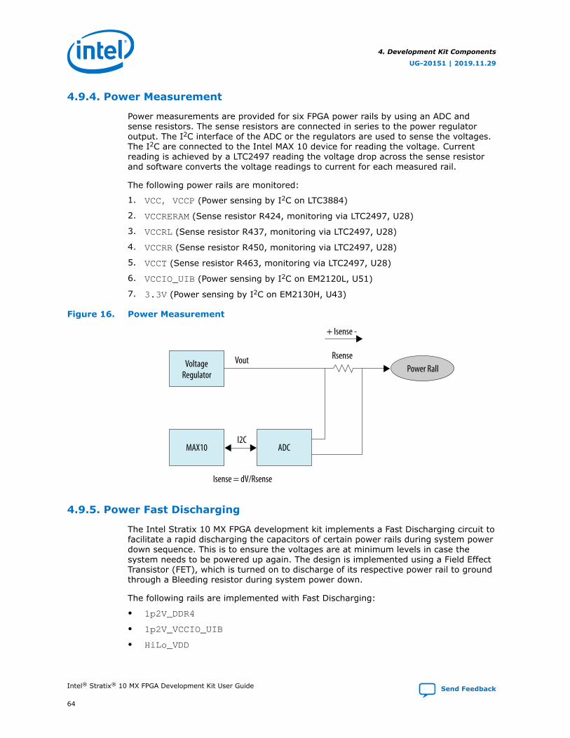
4.9.4. Power Measurement
Power measurements are provided for six FPGA power rails by using an ADC andsense resistors. The sense resistors are connected in series to the power regulatoroutput. The I2C interface of the ADC or the regulators are used to sense the voltages.The I2C are connected to the Intel MAX 10 device for reading the voltage. Currentreading is achieved by a LTC2497 reading the voltage drop across the sense resistorand software converts the voltage readings to current for each measured rail.
The following power rails are monitored:
1. VCC, VCCP (Power sensing by I2C on LTC3884)
2. VCCRERAM (Sense resistor R424, monitoring via LTC2497, U28)
3. VCCRL (Sense resistor R437, monitoring via LTC2497, U28)
4. VCCRR (Sense resistor R450, monitoring via LTC2497, U28)
5. VCCT (Sense resistor R463, monitoring via LTC2497, U28)
6. VCCIO_UIB (Power sensing by I2C on EM2120L, U51)
7. 3.3V (Power sensing by I2C on EM2130H, U43)
Figure 16. Power Measurement
MAX10
VoltageRegulator
ADCI2C
Isense = dV/Rsense
Rsense
+ Isense -
VoutPower Rall
4.9.5. Power Fast Discharging
The Intel Stratix 10 MX FPGA development kit implements a Fast Discharging circuit tofacilitate a rapid discharging the capacitors of certain power rails during system powerdown sequence. This is to ensure the voltages are at minimum levels in case thesystem needs to be powered up again. The design is implemented using a Field EffectTransistor (FET), which is turned on to discharge of its respective power rail to groundthrough a Bleeding resistor during system power down.
The following rails are implemented with Fast Discharging:
• 1p2V_DDR4
• 1p2V_VCCIO_UIB
• HiLo_VDD
4. Development Kit Components
UG-20151 | 2019.11.29
Intel® Stratix® 10 MX FPGA Development Kit User Guide Send Feedback
64

• HiLo_VDDQ
• 3p3V
• 2p5V
• VCCM
• 1p8V
• S10_VCCRL_GXB
• S10_VCCRR_GXB
• S10_VCCT_GXB
• S10_VCCERAM
4.9.6. Thermal Limitations and Protection
The Intel Stratix 10 MX FPGA development kit is designed to operate in a typicallaboratory environment with an ambient temperature of approximately 25 °C. Thecooling solution provided with the development kit allows sufficient cooling for theboard to operate up to a maximum power consumption of 243 W under thisenvironment.
A MAX1619 device is connected to the Intel Stratix 10 MX FPGA internal temperaturediode to continuously monitor the FPGA internal temperature. In the meantime, adedicated FPGA TSD real-time monitor solution under ~\ip\onchip_sensors\ isadded to each transceiver or EMIF example design to monitor the temperatures ofboth FPGA core and each transceiver tile.
Based on the data from both MAX1619, and the Intel Stratix 10 MX FPGA will run atits maximum speed whenever any temperature is over 60 °C or immediately power offthe board whenever the temperature crosses 100 °C.
Caution: Remember to unplug the power supply when the board is powered off when thetemperature crosses 100 °C. Plug the power supply back again to ensure that theboard can be normally turned on/off again.
4.9.7. Cooling Design
The Intel Stratix 10 MX FPGA development kit utilizes air-cooled design to maintainproper cooling of the board at maximum loads. Air is forced to blow from the front tothe rear of the enclosure by two 40 mm x 40 mm fans. It requires a total airflow of 22CFM to cool the board with maximum power of 243 W at 25 °C. Top cover is requiredduring operations for proper cooling of the board.
Caution: Please ensure that the fan cable is connected during operation.
4. Development Kit Components
UG-20151 | 2019.11.29
Send Feedback Intel® Stratix® 10 MX FPGA Development Kit User Guide
65

4.9.8. Mechanical Information
The Intel Stratix 10 MX FPGA development kit is a PCIe form factor with the followingboard dimensions:
• Width = 4.376 inches
• Length = 10.8 inches
• Height = 1.37 inches
4. Development Kit Components
UG-20151 | 2019.11.29
Intel® Stratix® 10 MX FPGA Development Kit User Guide Send Feedback
66

Figure 17. Assembly View
4.9.9. Top Cover Removal
The Intel Stratix 10 MX FPGA development kit is designed to operate with the topcover enclosed during normal operations.
To gain access to the top side of the board for tasks such as replacing DIMM module,HiLo module, or probing of test points, the top cover can be removed by following theinstructions below:
1. Loosen the two thumb screws on the rear of the enclose
2. Lift the top cover upward until it stops
3. Slide the top cover backward and lift again to remove
4. Development Kit Components
UG-20151 | 2019.11.29
Send Feedback Intel® Stratix® 10 MX FPGA Development Kit User Guide
67

Figure 18. Top Cover Removal for Intel Stratix 10 MX FPGA development kit
Steps for removing the top cover
Loosen thumb screwsSlide top cover backward
1
Lift top cover upward
Note: Top cover is required for proper cooling of the board
2
3
Figure 19. Intel Stratix 10 MX FPGA development kit with top cover removed
4. Development Kit Components
UG-20151 | 2019.11.29
Intel® Stratix® 10 MX FPGA Development Kit User Guide Send Feedback
68

5. Board Test SystemThe Intel Stratix 10 MX FPGA Development Kit includes an application called BoardTest System (BTS) to test the functionality of this board. The BTS provides an easy-to-use Graphical User Interface (GUI) to alter functional settings and observe results. Youcan use the BTS to test board components, modify functional parameters, observeperformance and measure power usage.
The BTS communicates over the JTAG bus to a test design running in the Intel Stratix10 MX FPGA device. You can use the BTS to reconfigure the FPGA with test designsspecific to the functionality that you are testing.
The BTS is also useful as a reference for designing systems.
Figure 20. BTS GUI Home
UG-20151 | 2019.11.29
Send Feedback
Intel Corporation. All rights reserved. Agilex, Altera, Arria, Cyclone, Enpirion, Intel, the Intel logo, MAX, Nios,Quartus and Stratix words and logos are trademarks of Intel Corporation or its subsidiaries in the U.S. and/orother countries. Intel warrants performance of its FPGA and semiconductor products to current specifications inaccordance with Intel's standard warranty, but reserves the right to make changes to any products and servicesat any time without notice. Intel assumes no responsibility or liability arising out of the application or use of anyinformation, product, or service described herein except as expressly agreed to in writing by Intel. Intelcustomers are advised to obtain the latest version of device specifications before relying on any publishedinformation and before placing orders for products or services.*Other names and brands may be claimed as the property of others.
ISO9001:2015Registered

Figure 21. About BTS
5.1. Preparing the Board
Several designs are provided to test the major board features. Each design providesdata for one or more tabs in the application. The Configure Menu identifies theappropriate design to download to the FPGA for each tab.
After successful FPGA configuration, the appropriate tab appears that allows you toexercise the related board features. Highlights appear in the board picture around thecorresponding components.
The BTS communicates over the JTAG bus to a test design running in the FPGA. TheBTS and Power Monitor share the JTAG bus with other applications like the Nios IIdebugger and the Signal Tap II Embedded Logic Analyzer. Because the BTS is designedbased on the Intel Quartus Prime software, be sure to close other applications beforeyou use the BTS.
The BTS relies on the Intel Quartus Prime software's specific library. Before runningthe BTS, open the Intel Quartus Prime software to automatically set the environmentvariable $QUARTUS_ROOTDIR. The BTS uses this environment variable to locate theIntel Quartus Prime library. The version of Intel Quartus Prime software set in theQUARTUS_ROOTDIR environment variable should be newer than version 14.1. Forexample, the Development Kit Installer version 15.1 requires that the Intel QuartusPrime software 14.1 or later version to be installed.
Also, to ensure that the FPGA is configured successfully, you should install the latestIntel Quartus Prime software that can support the silicon on the development kit. Forthis board, we recommend you install Intel Quartus Prime version 18.0.1b261.
Please refer to the README.txt file under \examples\board_test_systemdirectory.
5.2. Running the Board Test System
5. Board Test System
UG-20151 | 2019.11.29
Intel® Stratix® 10 MX FPGA Development Kit User Guide Send Feedback
70

Before you begin
With the power to the board turned off, follow these steps:
1. Connect the USB cable to your PC and the board.
2. Check whether the board switches and jumpers are set according to yourpreferences.
3. Turn on the power to the board.
To ensure operating stability, keep the USB cable connected and the board powered onwhen running the demonstration application. The BTS cannot run correctly unless theUSB cable is attached and the board is powered on.
To run the BTS
1. Navigate to the <package dir>\examples\board_test_system directory andrun the BoardTestSystem.exe application.
2. A GUI appears, displaying the application tab corresponding to the design runningin the FPGA. If the design loaded in the FPGA is not supported by the BTS GUI,you receive a message prompting you to configure your board with a valid BTSdesign. Refer to the Configure Menu on configuring your board.
If some design is running in the FPGA, the BTS GUI loads the design file (.sof) inthe image folder to check the current running design in the FPGA, therefore the designrunning in the FPGA must be the same as the design file in the image folder.
5.3. Using the Board Test System
This section describes each tab in the BTS.
5.3.1. The Configure Menu
Use the Configure Menu to select the design you want to use. Each design exampletests different board features. Select a design from this menu and the correspondingtabs become active for testing.
5. Board Test System
UG-20151 | 2019.11.29
Send Feedback Intel® Stratix® 10 MX FPGA Development Kit User Guide
71

Figure 22. The Configure Menu
To configure the FPGA with a test system design, perform the followingsteps:
1. On the Configure menu, click the configure command that corresponds to thefunctionality you wish to test.
2. In the dialog box that appears, click Configure to download the correspondingdesign to the FPGA.
3. When configuration finishes, close Intel Quartus Prime if it's already open. Thedesign begins running in the FPGA. The corresponding GUI application tabs thatinterface with the design are now enabled.
Note: If you use the Intel Quartus Prime Programmer for configuration, rather than the BTSGUI, you may need to restart the GUI.
5.3.2. The Sys Info Tab
The Sys Info tab shows the board's current configuration. The tab displays thecontents of the Intel MAX 10 registers, the JTAG chain, the board's MAC address, andother details stored on the board.
Figure 23. The Sys Info Tab
5. Board Test System
UG-20151 | 2019.11.29
Intel® Stratix® 10 MX FPGA Development Kit User Guide Send Feedback
72

The following sections describe the controls of the Sys Info tab.
Board Information
The Board Information control displays static information about your board:
• Board Name: Indicates the official name of the board given by the BTS.
• Board Revision: Indicates the revision of the board.
• MAX Ver: Indicates the version of Intel MAX 10 code currently running on theboard.
JTAG Chain
The JTAG chain shows all the devices currently in the JTAG chain.
5.3.3. The QSFP Tab
This tab allows you to perform loopback tests on the QSFP ports.
5. Board Test System
UG-20151 | 2019.11.29
Send Feedback Intel® Stratix® 10 MX FPGA Development Kit User Guide
73

Figure 24. The QSFP Tab
The following sections describe the controls on the QSFP Tab
Status
Displays the following status information during a loopback test:
• PLL Lock: Shows the PLL locked or unlocked state.
• Pattern sync: Shows the pattern synced or not synced state. The pattern isconsidered synced when the start of the data sequence is detected.
• Details: Shows the PLL lock and pattern sync status:
Port
Allows you to specify which interface to test. The following port tests are available:
5. Board Test System
UG-20151 | 2019.11.29
Intel® Stratix® 10 MX FPGA Development Kit User Guide Send Feedback
74

• QSFP0 x4
• QSFP1 x4
PMA Setting
Allows you to make changes to the PMA parameters that affect the active transceiverinterface. The following settings are available for analysis:
• Serial Loopback: Routes signals between the transmitter and the receiver.
• VOD: Specifies the voltage output differential of the transmitter buffer.
• Pre-emphasis tap:
— 1st pre: Specifies the amount of pre-emphasis on the pre-tap of thetransmitter buffer.
— 1st post: Specifies the amount of pre-emphasis on the first post tap of thetransmitter buffer.
• Equalizer: Specifies the CLTE EQ Gain for the receiver.
• AC Gain: Specifies the CLTE AC Gain for the receiver.
• VGA: Specifies the VGA gain value.
Data Type
Specifies the type of data contained in the transactions. The following data types areavailable for analysis:
• PRBS 7: Selects pseudo-random 7-bit sequences.
• PRBS 15: Selects pseudo-random 15-bit sequences.
• PRBS 23: Selects pseudo-random 23-bit sequences.
• PRBS 31: Selects pseudo-random 31-bit sequences.
• HF: Selects highest frequency divide-by-2 data pattern 10101010.
• LF: Selects lowest frequency divide-by-33 data pattern.
5. Board Test System
UG-20151 | 2019.11.29
Send Feedback Intel® Stratix® 10 MX FPGA Development Kit User Guide
75

Error Control
Displays data errors detected during analysis and allows you to insert errors:
• Detected errors: Displays the number of data errors detected in the hardware.
• Inserted errors: Displays the number of errors inserted into the transmit datastream.
• Insert: Inserts a one-word error into the transmit data stream each time you clickthe button. Insert is only enabled during transaction performance analysis.
• Clear: Resets the Detected errors and Inserted errors counters to zeroes.
Loopback
• Start: Initiates the selected ports transaction performance analysis. Always clickClear before Start.
• Stop: Terminates transaction performance analysis.
• TX and RX performance bars: Show the percentage of maximum theoreticaldata rate that the requested transactions are able to achieve.
5.3.4. The PCIE Tab
This tab allows you to run a PCIe loopback test on your board. You can also load thedesign and use an oscilloscope to measure an eye diagram of the PCIe transmitsignals.
Figure 25. The PCIE Tab
5. Board Test System
UG-20151 | 2019.11.29
Intel® Stratix® 10 MX FPGA Development Kit User Guide Send Feedback
76

The following sections describe the controls on the PCIE tab.
Status
Displays the following status information during a loopback test:
• PLL Lock: Shows the PLL locked or unlocked state.
• Pattern sync: Shows the pattern synced or not synced state. The pattern isconsidered synced when the start of the data sequence is detected.
• Details: Shows the PLL lock and pattern sync status:
Port
PCIe x16 Gen3
PMA Setting
Allows you to make changes to the PMA parameters that affect the active transceiverinterface. The following settings are available for analysis:
5. Board Test System
UG-20151 | 2019.11.29
Send Feedback Intel® Stratix® 10 MX FPGA Development Kit User Guide
77

• Serial Loopback: Routes signals between the transmitter and the receiver.
• VOD: Specifies the voltage output differential of the transmitter buffer.
• Pre-emphasis tap:
— 1st pre: Specifies the amount of pre-emphasis on the pre-tap of thetransmitter buffer.
— 1st post: Specifies the amount of pre-emphasis on the first post tap of thetransmitter buffer.
• Equalizer: Specifies the CLTE EQ Gain for the receiver.
• AC Gain: Specifies the CLTE AC Gain for the receiver.
• VGA: Specifies the VGA gain value.
All PMA settings should be changed as given in the figure below:
5. Board Test System
UG-20151 | 2019.11.29
Intel® Stratix® 10 MX FPGA Development Kit User Guide Send Feedback
78

Data Type
Specifies the type of data contained in the transactions. The following data types areavailable for analysis:
• PRBS 7: Selects pseudo-random 7-bit sequences.
• PRBS 15: Selects pseudo-random 15-bit sequences.
• PRBS 23: Selects pseudo-random 23-bit sequences.
• PRBS 31: Selects pseudo-random 31-bit sequences.
• HF: Selects highest frequency divide-by-2 data pattern 10101010.
• LF: Selects lowest frequency divide-by-33 data pattern.
Error Control
Displays data errors detected during analysis and allows you to insert errors:
5. Board Test System
UG-20151 | 2019.11.29
Send Feedback Intel® Stratix® 10 MX FPGA Development Kit User Guide
79

• Detected errors: Displays the number of data errors detected in the hardware.
• Inserted errors: Displays the number of errors inserted into the transmit datastream.
• Insert error: Inserts a one-word error into the transmit data stream each timeyou click the button. Insert error is only enabled during transaction performanceanalysis.
• Clear: Resets the detected errors and inserted errors counters to zeroes.
Loopback
• Start: Initiates the selected port's transaction performance analysis. Always clickClear before Start.
• Stop: Terminates transaction performance analysis.
• TX and RX performance bars: Show the percentage of maximum theoreticaldata rate that the requested transactions are able to achieve.
5.3.5. The Component DDR4 Tab
This tab allows you to read and write Component DDR4 memory on your board.
Figure 26. The Component DDR4 Tab
The following sections describe the controls on the Component DDR4 tab.
5. Board Test System
UG-20151 | 2019.11.29
Intel® Stratix® 10 MX FPGA Development Kit User Guide Send Feedback
80

Start
Initiates DDR4 memory transaction performance analysis.
Stop
Terminates transaction performance analysis.
Performance Indicator
These controls display current transaction performance analysis information collectedsince you last clicked Start:
• Write, Read and Total performance bars: Show the percentage of maximumtheoretical data rate that the requested transactions are able to achieve.
• Write (MBps), Read (MBps) and Total (MBps): Show the number of bytesanalyzed per second.
• Data Bus: 72 bits(8 bits ECC) wide and the frequency is 1066 MHz double datarate. 2133 Mbps per pin. Equating to a theoretical maximum bandwidth of136,512 Mbps or 17,064 MBps.
Error Control
This control displays data errors detected during analysis and allows you to inserterrors:
• Detected errors: Displays the number of data errors detected in the hardware.
• Inserted errors: Displays the number of errors inserted into the transactionstream.
• Insert: Inserts a one-word error into the transaction stream each time you clickthe button. Insert Error is only enabled during transaction performance analysis.
• Clear: Resets the detected error and inserted error counters to zeroes.
Address Range
Determines the number of addresses to use in each iteration of reads and writes.
5.3.6. The HiLo DDR4 Tab
This tab allows you to read and write HiLo DDR4 memory on your board.
5. Board Test System
UG-20151 | 2019.11.29
Send Feedback Intel® Stratix® 10 MX FPGA Development Kit User Guide
81

Figure 27. The HiLo DDR4 Tab
The following sections describe the controls on the DDR4 tab.
Start
Initiates DDR4 memory transaction performance analysis.
Stop
Terminates transaction performance analysis.
Performance Indicators
These controls display current transaction performance analysis information collectedsince you last clicked Start:
• Write, Read and Total performance bars: Show the percentage of maximumtheoretical data rate that the requested transactions are able to achieve.
• Write (MBps), Read (MBps) and Total (MBps): Show the number of bytesanalyzed per second.
• Data Bus: 72 bits (8 bits ECC) wide and the frequency is 1066 MHz double datarate. 2133 Mbps per pin. Equating to a theoretical maximum bandwidth of136,512 Mbps or 17,064 MBps.
Error Control
This control displays data errors detected during analysis and allows you to inserterrors:
5. Board Test System
UG-20151 | 2019.11.29
Intel® Stratix® 10 MX FPGA Development Kit User Guide Send Feedback
82

• Detected errors: Displays the number of data errors detected in the hardware.
• Inserted errors: Displays the number of errors inserted into the transactionstream.
• Insert: Inserts a one-word error into the transaction stream each time you clickthe button. Insert Error is only enabled during transaction performance analysis.
• Clear: Resets the detected error and inserted error counters to zeroes.
Address Range
Determines the number of addresses to use in each iteration of reads and writes.
5.3.7. The DDR4 Dimm Tab
This tab allows you to read and write Dual Inline Memory Module (DIMM) DDR4memory on your board.
Figure 28. The DDR4 Dimm Tab
The following sections describe the controls on the DDR4 tab.
Start
Initiates DDR4 memory transaction performance analysis.
Stop
Terminates transaction performance analysis.
5. Board Test System
UG-20151 | 2019.11.29
Send Feedback Intel® Stratix® 10 MX FPGA Development Kit User Guide
83

Performance Indicators
These controls display current transaction performance analysis information collectedsince you last clicked Start:
• Write, Read and Total performance bars: Show the percentage of maximumtheoretical data rate that the requested transactions are able to achieve.
• Write (MBps), Read (MBps) and Total (MBps): Show the number of bytesanalyzed per second.
• Data Bus: 72 bits (8 bits ECC) wide and the frequency is 1066 MHz double datarate. 2133 Mbps per pin. Equating to a theoretical maximum bandwidth of136,512 Mbps or 17,064 MBps.
Error Control
This control displays data errors detected during analysis and allows you to inserterrors:
• Detected errors: Displays the number of data errors detected in the hardware.
• Inserted errors: Displays the number of errors inserted into the transactionstream.
• Insert: Inserts a one-word error into the transaction stream each time you clickthe button. Insert Error is only enabled during transaction performance analysis.
• Clear: Resets the detected error and inserted error counters to zeroes.
Address Range
Determines the number of addresses to use in each iteration of reads and writes.
5.3.8. The HBM2 Top Tab
This tab allows you to read and write the top bank of HBM2 on your board.
5. Board Test System
UG-20151 | 2019.11.29
Intel® Stratix® 10 MX FPGA Development Kit User Guide Send Feedback
84

Figure 29. The HBM2 Top Tab
The following sections describe the controls on the HBM2 tab.
Status Indicators
• HBM2 Size: Indicates the memory size of HBM2.
• Test Status: Indicates the status of the overall test, the table shows each channelstatus of HBM2.
5.3.9. The HBM2 Bottom Tab
This tab allows you to read and write the bottom bank of HBM2 on your board.
5. Board Test System
UG-20151 | 2019.11.29
Send Feedback Intel® Stratix® 10 MX FPGA Development Kit User Guide
85

Figure 30. The HBM2 Bottom Tab
The following sections describe the controls on the HBM2 tab.
Status Indicators
• HBM2 Size: Indicates the memory size of HBM2.
• Test Status: Indicates the status of the overall test, the table shows each channelstatus of HBM2.
5.3.10. Power Monitor
The Power Monitor measures and reports current power information andcommunicates with the Intel MAX 10 device on the board through the JTAG bus. Apower monitor circuit attached to the Intel MAX 10 device allows you to measure thepower that the Intel Stratix 10 MX FPGA is consuming.
To start the application, click the Power Monitor icon in the BTS. You can also runthe Power Monitor as a stand-alone application. The PowerMonitor.exe resides inthe <package dir>\examples\board_test_system directory.
Note: You cannot run the stand-alone power application and the BTS simultaneously. Also,you cannot run power and clock interface at the same time.
5. Board Test System
UG-20151 | 2019.11.29
Intel® Stratix® 10 MX FPGA Development Kit User Guide Send Feedback
86

Figure 31. Power Monitor Interface
The controls on the Power Monitor are described below.
Test Settings
• Power Rails: Indicates the currently selected power rail. After selecting thedesired rail, click Reset to refresh the screen with updated board readings.
• Scale: Specifies the amount to scale the power graph. Select a smaller number tozoom-in to see finer detail. Select a larger number to zoom-out to view the entirerange of recorded values.
• Speed: Specifies how often to refresh the graph.
Power Information
Displays the root mean square (RMS) current, maximum and minimum numericalpower readings in mA.
Graph
Displays the mA power consumption of your board over time. The green line indicatesthe current value. The red line indicates the maximum value read since the last reset.The yellow line indicates the minimum value read since the last reset.
General Information
Displays the Intel MAX 10 version and current temperature of the FPGA and the board.
5. Board Test System
UG-20151 | 2019.11.29
Send Feedback Intel® Stratix® 10 MX FPGA Development Kit User Guide
87

Reset
Clears the graph, resets the minimum and maximum values and restarts the PowerMonitor.
5.3.11. Clock Controller
The Clock Controller application sets the Si5338 programmable oscillators to anyfrequency between 0.16 MHz and 710 MHz.
The Clock Controller application sets the Si5341 programmable oscillators to anyfrequency between 0.1 MHz and 712.5 MHz.
The Clock Control communicates with the Intel MAX 10 on the board through the JTAGbus. The programmable oscillator are connected to the Intel MAX 10 device through a2-wire serial bus.
Figure 32. Clock Controller - Si5338
5. Board Test System
UG-20151 | 2019.11.29
Intel® Stratix® 10 MX FPGA Development Kit User Guide Send Feedback
88

Figure 33. Clock Controller - Si5341
Si5338 tab and Si5341 tab display the same GUI controls for each clock generators.Each tab allows for separate control. The Si5338 is capable of synthesizing fourindependent user-programmable clock frequencies up to 710 MHz.
The controls of the clock controller are described below:
F_vco
Displays the generating signal value of the voltage-controlled oscillator.
Register
Display the current frequencies for each oscillator.
Frequency
Allows you to specify the frequency of the clock MHz.
Read
Reads the current frequency setting for the oscillator associated with the active tab.
5. Board Test System
UG-20151 | 2019.11.29
Send Feedback Intel® Stratix® 10 MX FPGA Development Kit User Guide
89

Default
Sets the frequency for the oscillator associated with the active tab back to its defaultvalue. This can also be accomplished by power cycling the board.
Set
Sets the programmable oscillator frequency for the selected clock to the value in theCLK0 to CLK3 controls for the Si5338. Frequency changes might take severalmilliseconds to take effect. You might see glitches on the clock during this time. Intelrecommends resetting the FPGA logic after changing frequencies.
Import
Import register map file generated from Silicon Laboratories ClockBuilder Desktop.
5. Board Test System
UG-20151 | 2019.11.29
Intel® Stratix® 10 MX FPGA Development Kit User Guide Send Feedback
90

A. Additional Information
A.1. Add SmartVID settings in the QSF file
Intel Stratix 10 FPGA silicon assembled on the Intel Stratix 10 MX FPGA DevelopmentKit enables SmartVID feature by default.
You may encounter the following error message when you switch from using theexample design to your own design:
Error(19192): File <filename>.sof is incomplete - Power management settings are notset up appropriately on VID part"
To prevent Intel Quartus Prime from generating an error message due to incompleteSmartVID settings, you must put constraints listed below into the Intel Quartus Primeproject QSF file.
Open your Intel Quartus Prime project QSF file, copy and paste the constraints listedbelow in the QSF file.
Before, you compile your project with correct SmartVID settings, ensure that there areno other similar settings with different values.
Constraints
set_global_assignment -name VID_OPERATION_MODE "PMBUS MASTER"
set_global_assignment -name USE_PWRMGT_SCL SDM_IO14
set_global_assignment -name USE_PWRMGT_SDA SDM_IO11
set_global_assignment -name USE_CONF_DONE SDM_IO16
set_global_assignment -name USE_INIT_DONE SDM_IO0
set_global_assignment -name PWRMGT_BUS_SPEED_MODE "400 KHZ"
set_global_assignment -name PWRMGT_SLAVE_DEVICE0_ADDRESS 4F
set_global_assignment -name PWRMGT_PAGE_COMMAND_ENABLE ON
The Intel Stratix 10 device family offers SmartVID standard power devices in all speedgrades. Lower power fixed-voltage devices are also available in all speed gradesexcept for the fastest speed grade. Please refer to Intel Stratix 10 Power ManagementUser Guide for additional information.
Related Information
Intel Stratix 10 Power Management User Guide
UG-20151 | 2019.11.29
Send Feedback
Intel Corporation. All rights reserved. Agilex, Altera, Arria, Cyclone, Enpirion, Intel, the Intel logo, MAX, Nios,Quartus and Stratix words and logos are trademarks of Intel Corporation or its subsidiaries in the U.S. and/orother countries. Intel warrants performance of its FPGA and semiconductor products to current specifications inaccordance with Intel's standard warranty, but reserves the right to make changes to any products and servicesat any time without notice. Intel assumes no responsibility or liability arising out of the application or use of anyinformation, product, or service described herein except as expressly agreed to in writing by Intel. Intelcustomers are advised to obtain the latest version of device specifications before relying on any publishedinformation and before placing orders for products or services.*Other names and brands may be claimed as the property of others.
ISO9001:2015Registered

A.2. Safety and Regulatory Information
ENGINEERING DEVELOPMENT PRODUCT - NOT FOR RESALE OR LEASE
This development kit is intended for laboratory development and engineering use only.
This development kit is designed to allow:
• Product developers and system engineers to evaluate electronic components,circuits, or software associated with the development kit to determine whether toincorporate such items in a finished product.
• Software developers to write software applications for use with the end product.
This kit is not a finished product and when assembled may not be resold or otherwisemarketed unless all required Federal Communications Commission (FCC) equipmentauthorizations are first obtained.
Operation is subject to the condition that this product not cause harmful interferenceto licensed radio stations and that this product accept harmful interference.
Unless the assembled kit is designed to operate under Part 15, Part 18 or Part 95 ofthe United States Code of Federal Regulations (CFR) Title 47, the operator of the kitmust operate under the authority of an FCC licenseholder or must secure anexperimental authorization under Part 5 of the United States CFR Title 47.
Safety Assessment and CE mark requirements have been completed, however, othercertifications that may be required for installation and operation in your region havenot been obtained.
A.2.1. Safety Warnings
Power Supply Hazardous Voltage
AC mains voltages are present within the power supply assembly. No user serviceableparts are present inside the power supply.
A. Additional Information
UG-20151 | 2019.11.29
Intel® Stratix® 10 MX FPGA Development Kit User Guide Send Feedback
92

Power Connect and Disconnect
The AC power supply cord is the primary disconnect device from mains (AC power)and used to remove all DC power from the board/system. The socket outlet must beinstalled near the equipment and must be readily accessible.
System Grounding (Earthing)
To avoid shock, you must ensure that the power cord is connected to a properly wiredand grounded receptacle. Ensure that any equipment to which this product is attachedis also connected to properly wired and grounded receptacles.
Power Cord Requirements
The connector that plugs into the wall outlet must be a grounding-type male plugdesigned for use in your region. It must have marks showing certification by anagency in your region. The connector that plugs into the AC receptacle on the powersupply must be an IEC 320, sheet C13, female connector. If the power cord suppliedwith the system does not meet requirements for use in your region, discard the cordand do not use it with adapters.
A. Additional Information
UG-20151 | 2019.11.29
Send Feedback Intel® Stratix® 10 MX FPGA Development Kit User Guide
93

Lightning/Electrical Storm
Do not connect/disconnect any cables or perform installation/maintenance of thisproduct during an electrical storm.
Risk of Fire
To reduce the risk of fire, keep all flammable materials a safe distance away from theboards and power supply. You must configure the development kit on a flameretardant surface.
A.2.2. Safety Cautions
Caution: Hot Surfaces and Sharp Edges. Integrated Circuits and heat sinks may be hot if thesystem has been running. Also, there might be sharp edges on some boards. Contactshould be avoided.
Thermal and Mechanical Injury
Certain components such as heat sinks, power regulators, and processors may be hot.Heatsink fans are not guarded. Power supply fan may be accessible through guard.Care should be taken to avoid contact with these components.
A. Additional Information
UG-20151 | 2019.11.29
Intel® Stratix® 10 MX FPGA Development Kit User Guide Send Feedback
94

Cooling Requirements
Maintain a minimum clearance area of 5 centimeters (2 inches) around the side, frontand back of the board for cooling purposes. Do not block power supply ventilationholes and fan.
Electro-Magnetic Interference (EMI)
This equipment has not been tested for compliance with emission limits of FCC andsimilar international regulations. Use of this equipment in a residential location isprohibited. This equipment generates, uses and can radiate radio frequency energywhich may result in harmful interference to radio communications. If this equipmentdoes cause harmful interference to radio or television reception, which can bedetermined by turning the equipment on and off, the user is required to takemeasures to eliminate this interference.
Telecommunications Port Restrictions
The wireline telecommunications ports (modem, xDSL, T1/E1) on this product mustnot be connected to the Public Switched Telecommunication Network (PSTN) as itmight result in disruption of the network. No formal telecommunication certification toFCC, R&TTE Directive, or other national requirements have been obtained.
Electrostatic Discharge (ESD) Warning
A properly grounded ESD wrist strap must be worn during operation/installation of theboards, connection of cables, or during installation or removal of daughter cards.Failure to use wrist straps can damage components within the system.
A. Additional Information
UG-20151 | 2019.11.29
Send Feedback Intel® Stratix® 10 MX FPGA Development Kit User Guide
95

Attention: Please return this product to Intel for proper disposition. If it is not returned,refer to local environmental regulations for proper recycling. Do not disposeof this product in unsorted municipal waste.
Ecology Conformance Marking for WEEE and China RoHS
A.3. Compliance and Conformity Statement
CE EMI Conformity Caution
This development kit is delivered conforming to relevant standards mandated byDirective 2014/30/EU. Because of the nature of programmable logic devices, it ispossible for the user to modify the development kit in such a way as to generateelectromagnetic interference (EMI) that exceeds the limits established for thisequipment. Any EMI caused as a result of modifications to the delivered material is theresponsibility of the user of this development kit.
A. Additional Information
UG-20151 | 2019.11.29
Intel® Stratix® 10 MX FPGA Development Kit User Guide Send Feedback
96

B. Revision History
B.1. Revision History for Intel Stratix 10 MX FPGA Development KitUser Guide
DocumentVersion
Changes
2019.11.29 • Add support for production versions of development board:— Intel Stratix 10 MX FPGA H-Tile (8 GB)— Intel Stratix 10 MX FPGA H-Tile (16 GB)
• Remove support for ES version of development board
2019.09.20 Updated SW2 DIP JTAG Switch Default Settings (Board Bottom) Table in Default Switch and JumperSettings on page 12
2019.08.22 Added Add SmartVID settings in the QSF file on page 91
2018.10.12 Engineering Silicon (ES) Release.
UG-20151 | 2019.11.29
Send Feedback
Intel Corporation. All rights reserved. Agilex, Altera, Arria, Cyclone, Enpirion, Intel, the Intel logo, MAX, Nios,Quartus and Stratix words and logos are trademarks of Intel Corporation or its subsidiaries in the U.S. and/orother countries. Intel warrants performance of its FPGA and semiconductor products to current specifications inaccordance with Intel's standard warranty, but reserves the right to make changes to any products and servicesat any time without notice. Intel assumes no responsibility or liability arising out of the application or use of anyinformation, product, or service described herein except as expressly agreed to in writing by Intel. Intelcustomers are advised to obtain the latest version of device specifications before relying on any publishedinformation and before placing orders for products or services.*Other names and brands may be claimed as the property of others.
ISO9001:2015Registered