interconnect/via - concordia universityusers.encs.concordia.ca/~asim/coen 451/lectures/w... ·...
TRANSCRIPT
CONCORDIAVLSI DESIGN LAB
1
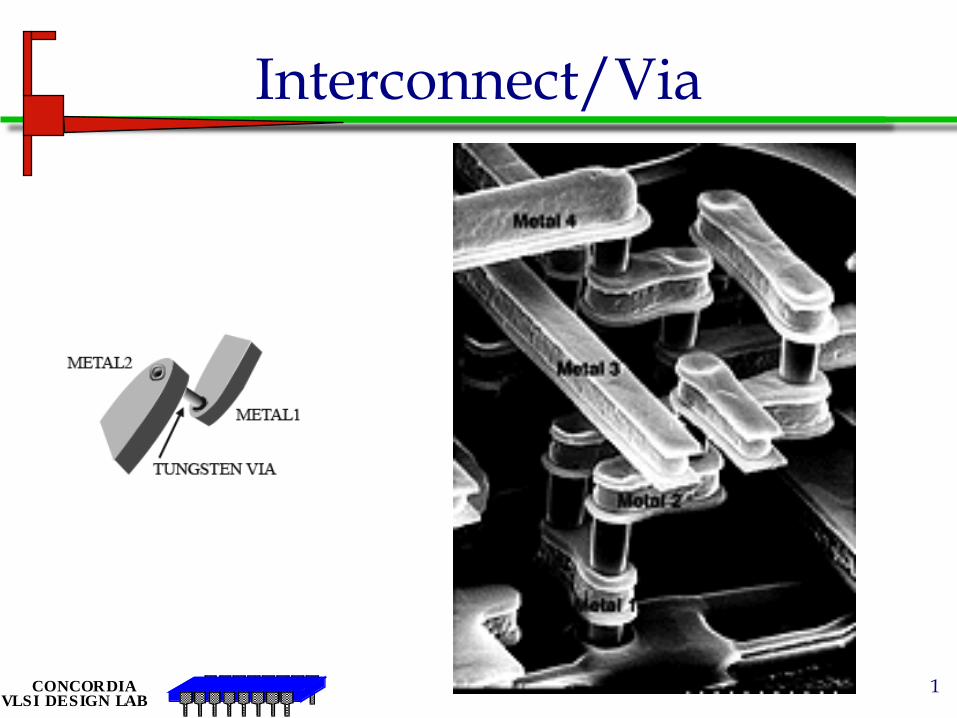
Interconnect/Via
CONCORDIAVLSI DESIGN LAB
2
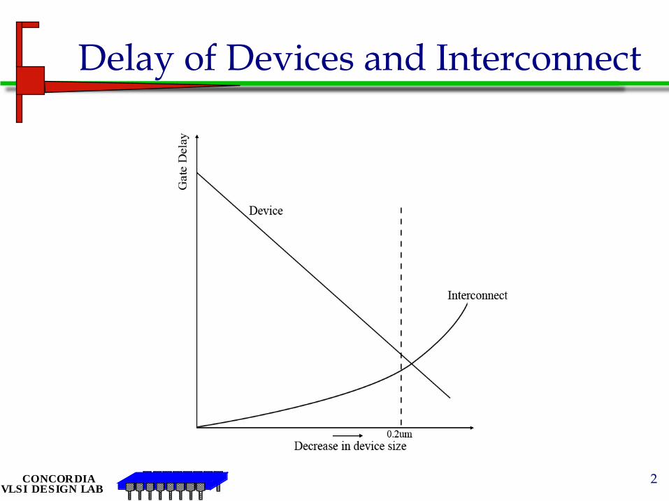
Delay of Devices and Interconnect
CONCORDIAVLSI DESIGN LAB
3
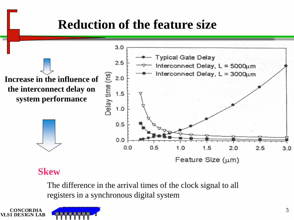
Reduction of the feature size
Increase in the influence of
the interconnect delay on
system performance
The difference in the arrival times of the clock signal to all
registers in a synchronous digital system
Skew
CONCORDIAVLSI DESIGN LAB
4
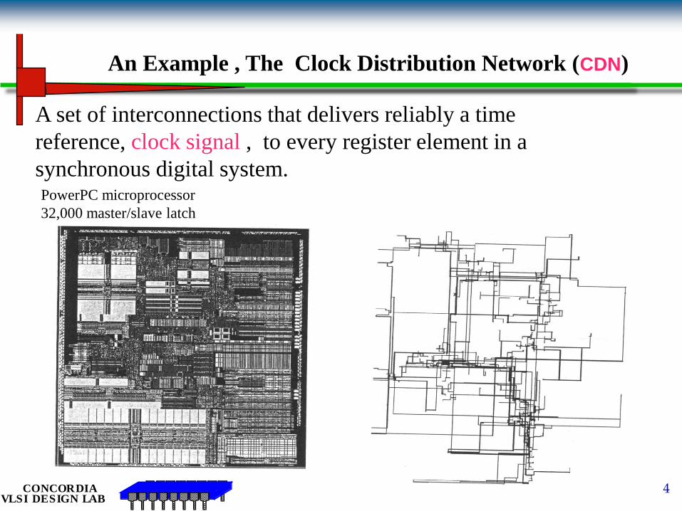
PowerPC microprocessor
32,000 master/slave latch
An Example , The Clock Distribution Network (CDN)
A set of interconnections that delivers reliably a time
reference, clock signal , to every register element in a
synchronous digital system.
CONCORDIAVLSI DESIGN LAB
5
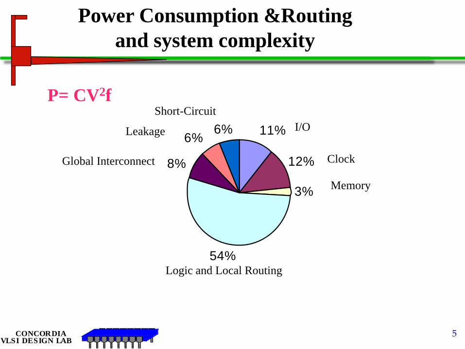
11%
12%
3%
54%
8%
6%6%
Memory
Leakage
Short-Circuit
Clock
I/O
Global Interconnect
Logic and Local Routing
Power Consumption &Routing
and system complexity
P= CV2f
CONCORDIAVLSI DESIGN LAB
6
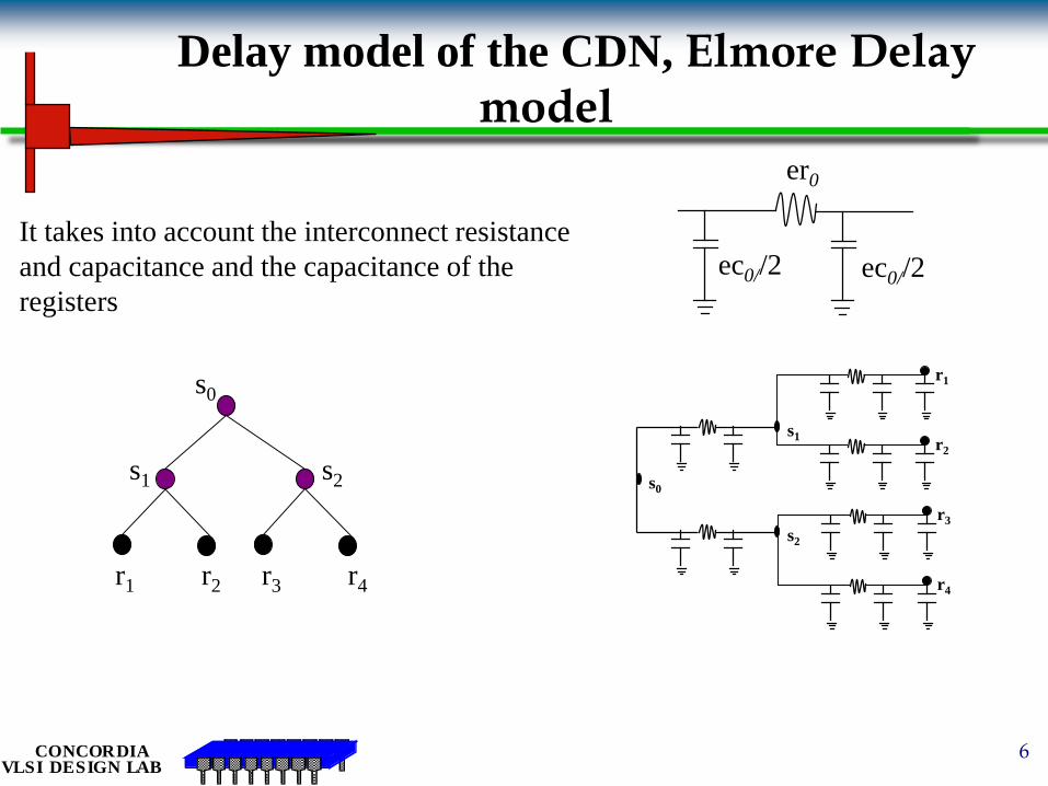
Delay model of the CDN, Elmore Delay model
r1 r2
s1
r4r3
s2
s0
It takes into account the interconnect resistance
and capacitance and the capacitance of the
registers
ec0//2
er0
ec0//2
s1
r1
r2
s2
r3
r4
s0
CONCORDIAVLSI DESIGN LAB
7
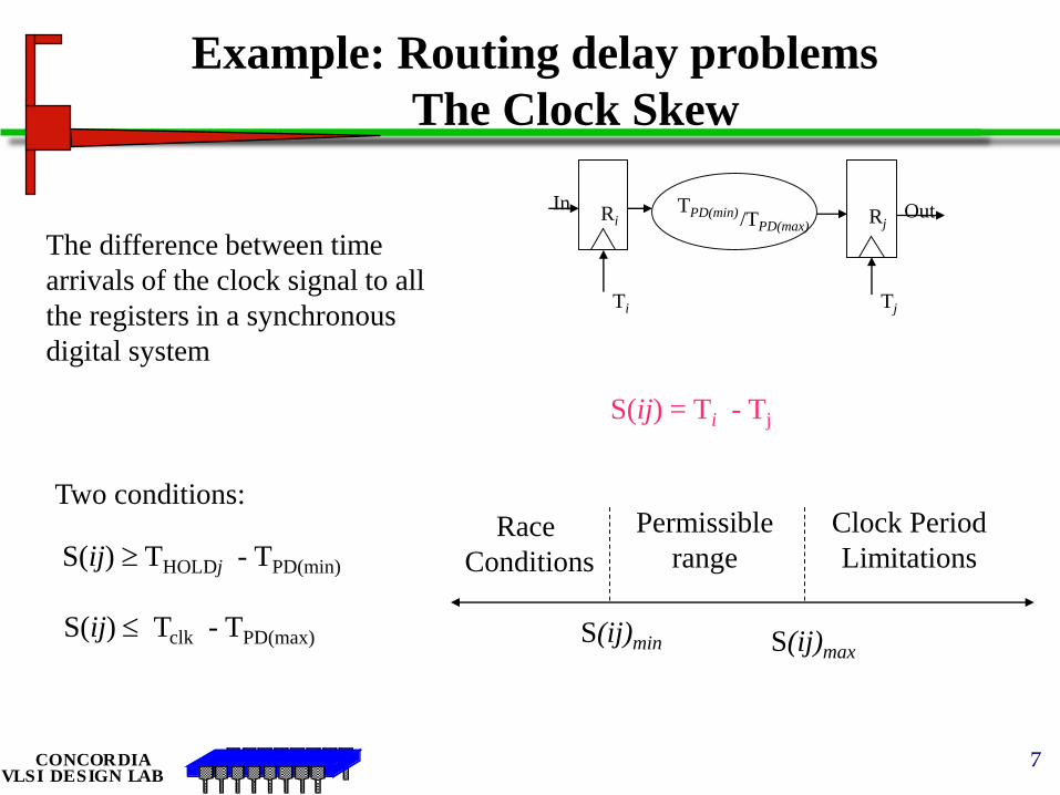
OutInRi Rj
Ti Tj
TPD(min) /TPD(max)
Example: Routing delay problems
The Clock Skew
The difference between time
arrivals of the clock signal to all
the registers in a synchronous
digital system
S(ij) = Ti - Tj
Clock Period
Limitations
Permissible
rangeRace
Conditions
S(ij)min S(ij)max
S(ij) THOLDj - TPD(min)
S(ij) Tclk - TPD(max)
Two conditions:
CONCORDIAVLSI DESIGN LAB
8
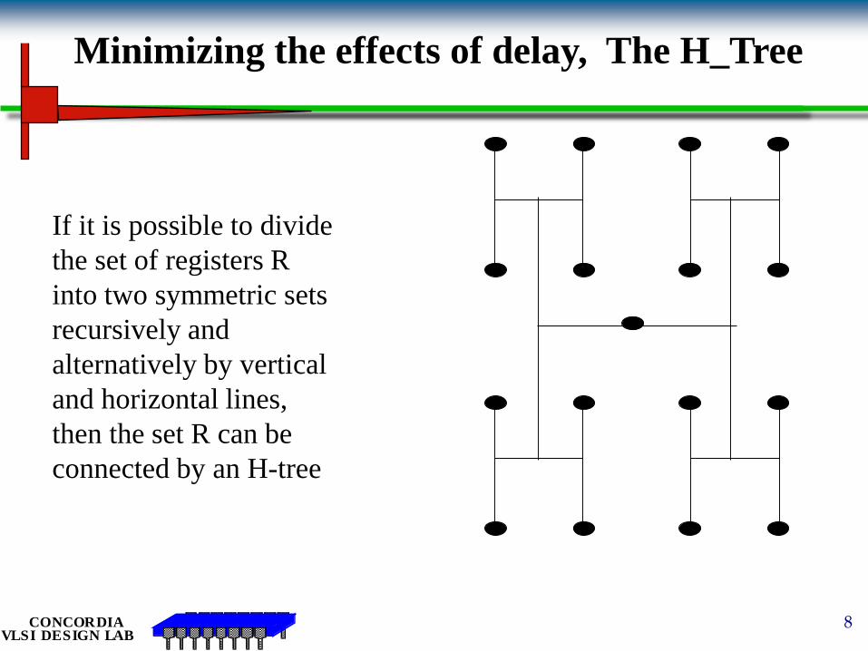
Minimizing the effects of delay, The H_Tree
If it is possible to divide
the set of registers R
into two symmetric sets
recursively and
alternatively by vertical
and horizontal lines,
then the set R can be
connected by an H-tree

CONCORDIAVLSI DESIGN LAB
9
Interconnect Length

CONCORDIAVLSI DESIGN LAB
10
Interconnect/Via
CONCORDIAVLSI DESIGN LAB
11
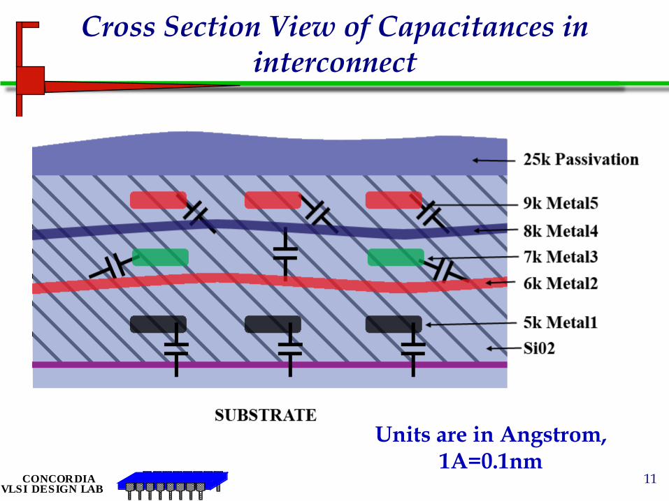
Cross Section View of Capacitances in interconnect
Units are in Angstrom, 1A=0.1nm
CONCORDIAVLSI DESIGN LAB
12
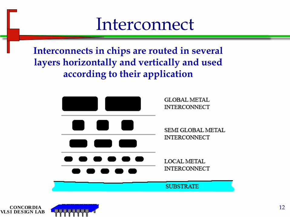
Interconnect
Interconnects in chips are routed in several layers horizontally and vertically and used
according to their application

CONCORDIAVLSI DESIGN LAB
Small line length: transistor speed governs the circuit speed.
Medium line length Transistor output resistance andline capacitance govern the circuit speed.
Long line length, line resistance and line capacitance govern the circuit speed.
Cooling the room temperature to 77K reduces the resistivity by an order of magnitude.At higher frequencies, Ghz and above the skin effect has to be taken into account.
CONCORDIAVLSI DESIGN LAB
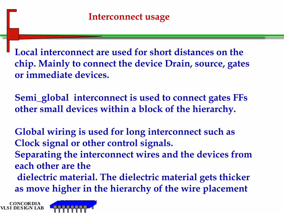
Local interconnect are used for short distances on the chip. Mainly to connect the device Drain, source, gates or immediate devices.
Semi_global interconnect is used to connect gates FFs other small devices within a block of the hierarchy.
Global wiring is used for long interconnect such as Clock signal or other control signals.Separating the interconnect wires and the devices from each other are thedielectric material. The dielectric material gets thicker as move higher in the hierarchy of the wire placement
Interconnect usage

CONCORDIAVLSI DESIGN LAB
15
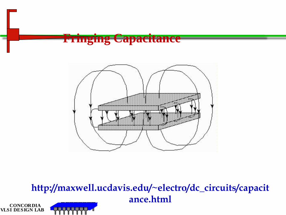
Parallel and fringing Capacitance
CONCORDIAVLSI DESIGN LAB
http://maxwell.ucdavis.edu/~electro/dc_circuits/capacitance.html
Fringing Capacitance
CONCORDIAVLSI DESIGN LAB
17
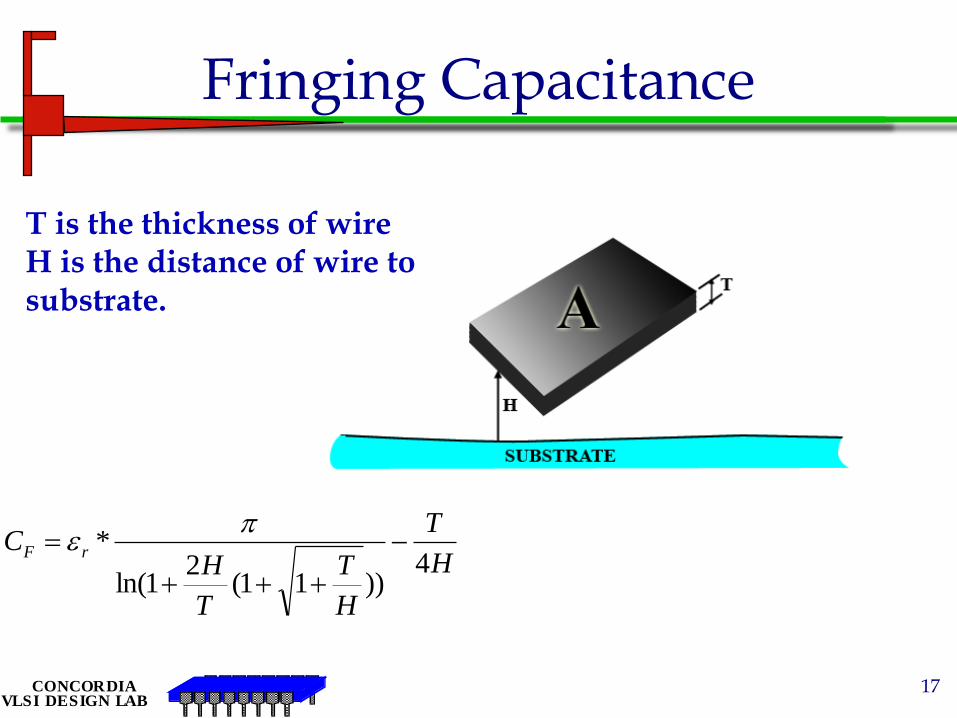
Fringing Capacitance
H
T
H
T
T
HC rF
4))11(
21ln(
*
T is the thickness of wire H is the distance of wire to substrate.

CONCORDIAVLSI DESIGN LAB
18
Cross Talk
CONCORDIAVLSI DESIGN LAB
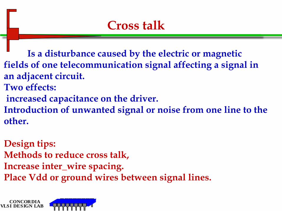
Cross talk
Is a disturbance caused by the electric or magnetic fields of one telecommunication signal affecting a signal in an adjacent circuit.Two effects:increased capacitance on the driver.
Introduction of unwanted signal or noise from one line to the other.
Design tips:Methods to reduce cross talk,Increase inter_wire spacing.Place Vdd or ground wires between signal lines.
CONCORDIAVLSI DESIGN LAB
20
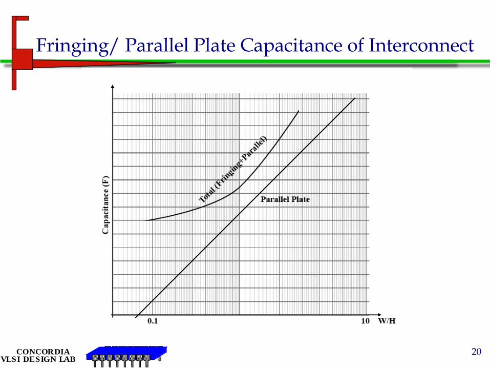
Fringing/ Parallel Plate Capacitance of Interconnect
CONCORDIAVLSI DESIGN LAB
21
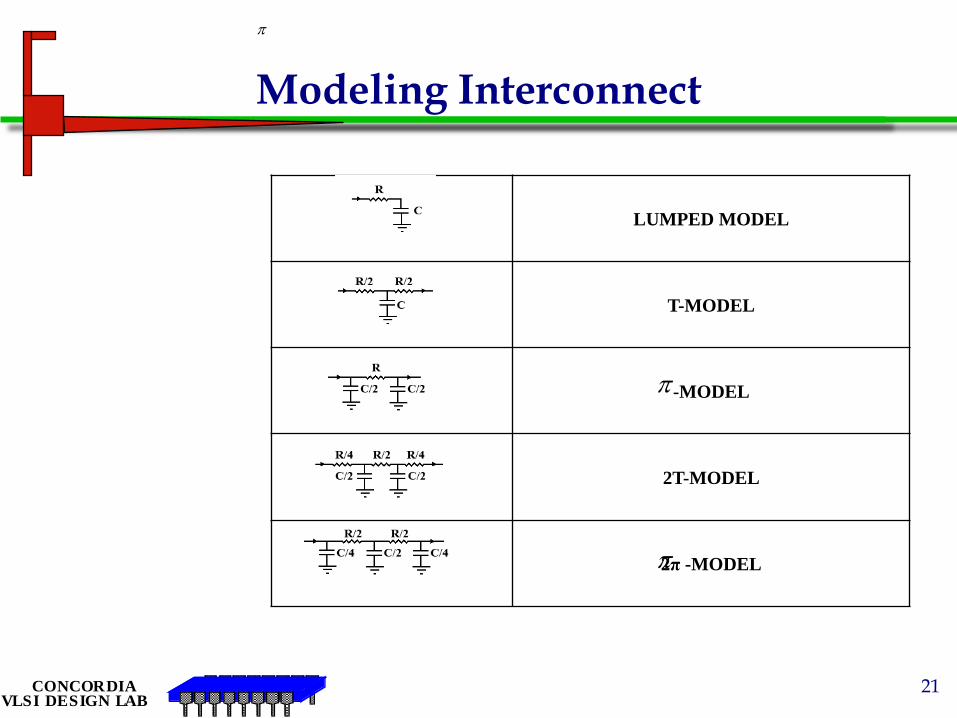
Modeling Interconnect
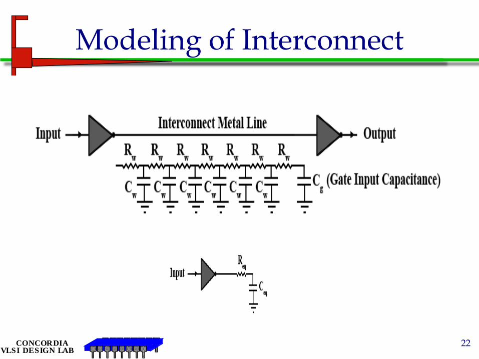
LUMPED MODEL
T-MODEL
-MODEL
2T-MODEL
2π -MODEL
CONCORDIAVLSI DESIGN LAB
22
Modeling of Interconnect
CONCORDIAVLSI DESIGN LAB
23
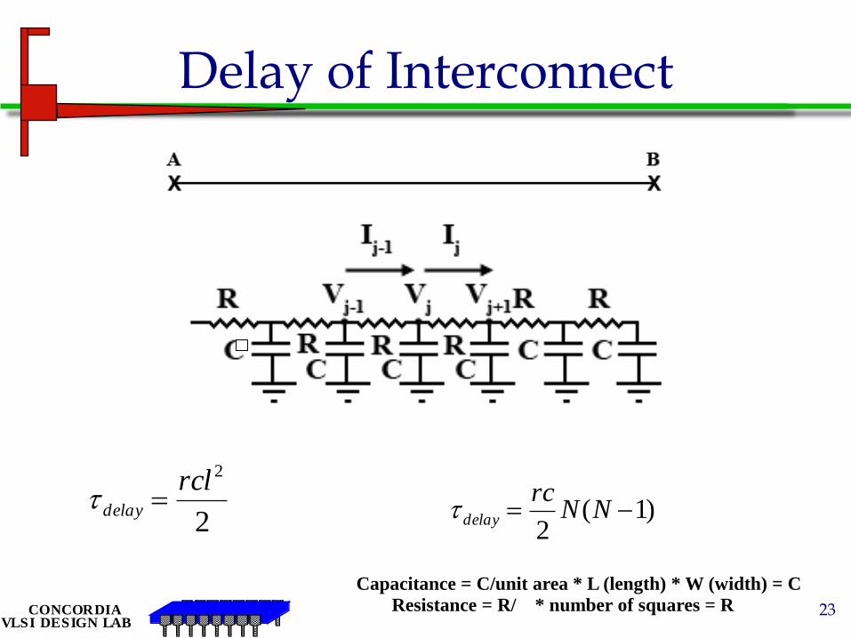
Delay of Interconnect
)1(2
NNrc
delay2
2rcldelay
Capacitance = C/unit area * L (length) * W (width) = C
Resistance = R/ * number of squares = R
CONCORDIAVLSI DESIGN LAB
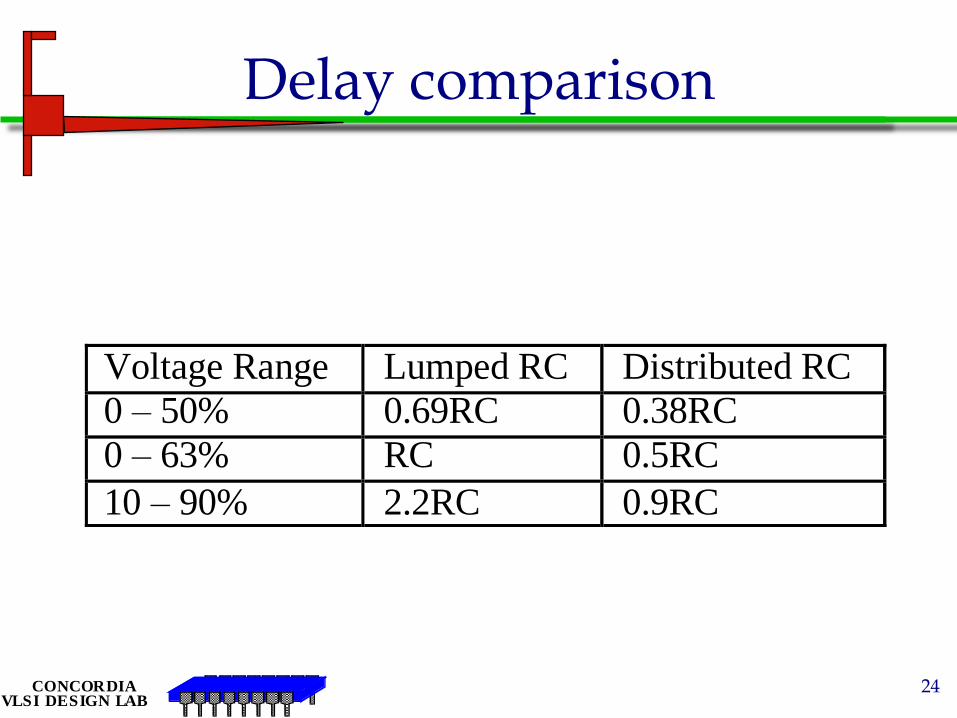
Delay comparison
24
Voltage Range Lumped RC Distributed RC
0 – 50% 0.69RC 0.38RC
0 – 63% RC 0.5RC
10 – 90% 2.2RC 0.9RC
CONCORDIAVLSI DESIGN LAB
RC delay with distributed parameters:
• More accurate than lumped RC model
• More difficult to solve for large N
• Need full-scale SPICE simulation
CONCORDIAVLSI DESIGN LAB
26
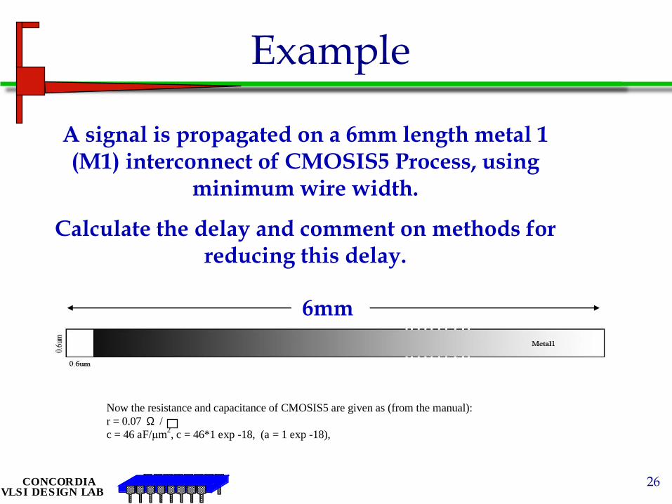
Example
A signal is propagated on a 6mm length metal 1 (M1) interconnect of CMOSIS5 Process, using
minimum wire width.
Calculate the delay and comment on methods for reducing this delay.
6mm
Now the resistance and capacitance of CMOSIS5 are given as (from the manual):
r = 0.07 W /
c = 46 aF/µm2, c = 46*1 exp -18, (a = 1 exp -18),
CONCORDIAVLSI DESIGN LAB
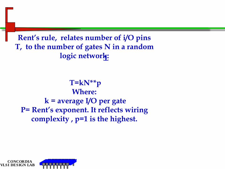
Rent’s rule, relates number of i/O pins T, to the number of gates N in a random
logic network:
T=kN**pWhere:
k = average I/O per gateP= Rent’s exponent. It reflects wiring
complexity , p=1 is the highest.T
CONCORDIAVLSI DESIGN LAB
28
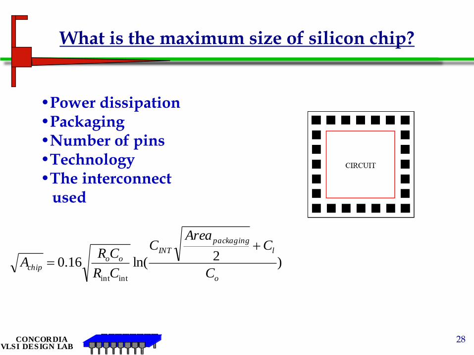
What is the maximum size of silicon chip?
)2ln(16.0intint o
l
packaging
INToo
chipC
CArea
C
CR
CRA
•Power dissipation•Packaging•Number of pins•Technology•The interconnect
used

CONCORDIAVLSI DESIGN LAB
29
Thank you !
CONCORDIAVLSI DESIGN LAB
30
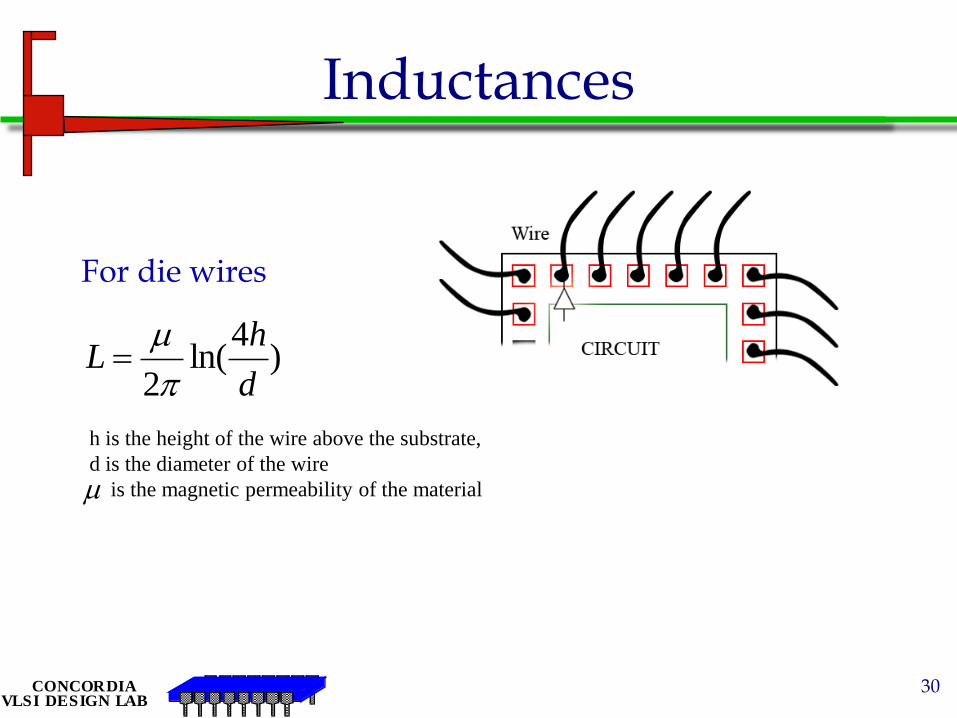
Inductances
)4
ln(2 d
hL
For die wires
h is the height of the wire above the substrate,
d is the diameter of the wire
is the magnetic permeability of the material
CONCORDIAVLSI DESIGN LAB
31
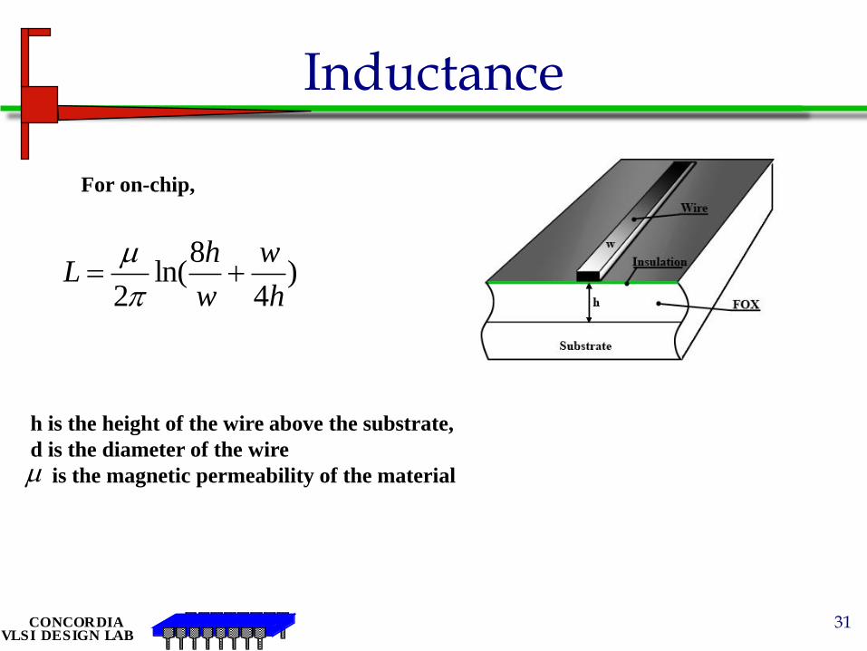
Inductance
For on-chip,
)4
8ln(
2 h
w
w
hL
h is the height of the wire above the substrate,
d is the diameter of the wire
is the magnetic permeability of the material
32
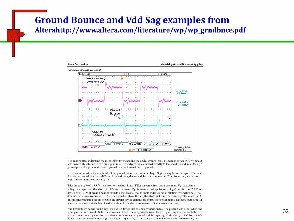
Ground Bounce and Vdd Sag examples from Alterahttp://www.altera.com/literature/wp/wp_grndbnce.pdf
CONCORDIAVLSI DESIGN LAB
33
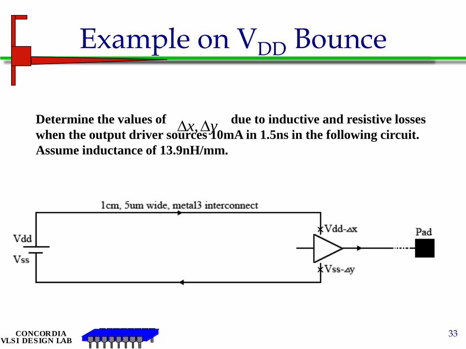
Example on VDD Bounce
yx ,Determine the values of due to inductive and resistive losses
when the output driver sources 10mA in 1.5ns in the following circuit.
Assume inductance of 13.9nH/mm.
CONCORDIAVLSI DESIGN LAB
34
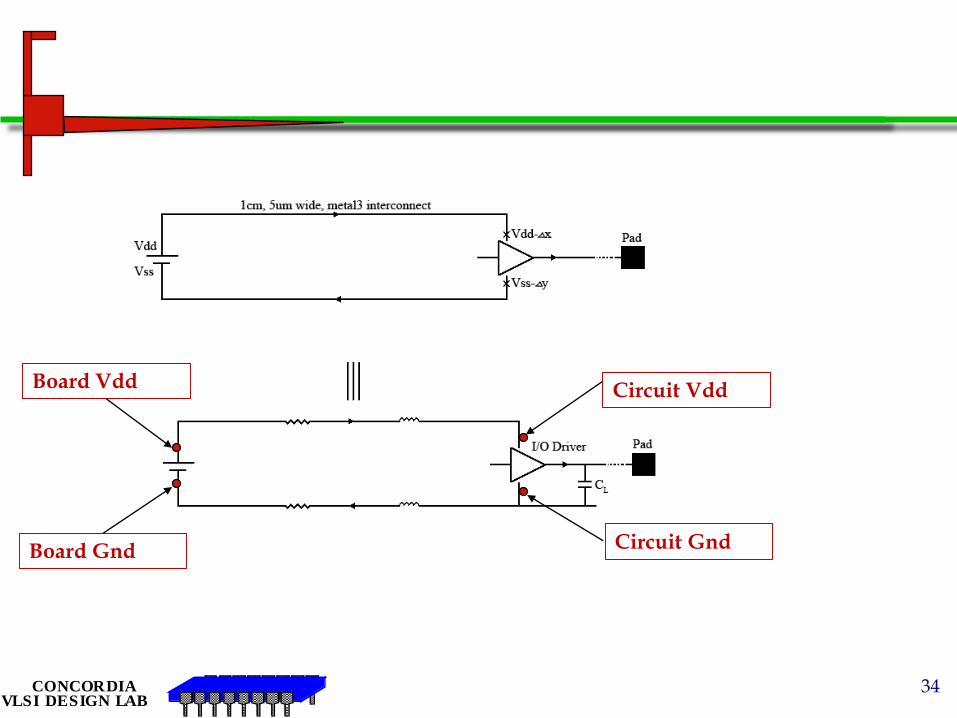
Circuit Vdd
Circuit GndBoard Gnd
Board Vdd
CONCORDIAVLSI DESIGN LAB
35
Example on Power lines
What will be the power line width if you drive a 10pF load at 1GHz
Assume Vdd=3.5V.
CONCORDIAVLSI DESIGN LAB
36
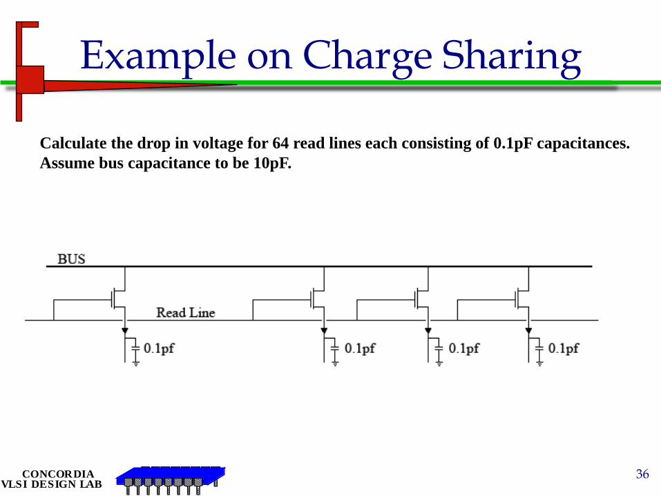
Example on Charge Sharing
Calculate the drop in voltage for 64 read lines each consisting of 0.1pF capacitances.
Assume bus capacitance to be 10pF.

CONCORDIAVLSI DESIGN LAB
37
Thank you !