interface and installation manual
TRANSCRIPT

INTERFACE AND
INSTALLATION MANUAL
OIG ITAL EQUIF'MENT CORPORATION ' MAYNARD, MASSACrlU5ET TS

PDP-7 INTERFACE AND
INSTALLATION MANUAL
F-78A 3/66
DIGITAL EQUIPMENT CORPORATION • MAYNARD, MASSACHUSETTS

Copyright 1966 by Digital Equipment Corporation
ii

Chapter
2
3
4
5
CONTENTS
INTRODUCTION •••.•••.••.•..•....•..•.••••••..••••••••••••••••..•.•••
Programmed Data Transfers .....••••....••.••••.•.••.••......•••..••.• 2
Data Break Transfers ....•...•..•.•••.••..•••.•.•.••••.••••••••.••••• 3
Pertinent Documents 3
Logic Symbols ... • • • • . . . . • . . . • • • • • . . • • • . • • • . • . • • • . • • . • . • • • . • . • • • . . • • 4
PROGRAMMED DATA TRANSFERS •.•....•.••...•••.•••••••.•••.••••.••.•• 7
TimingCycle ..•.•••..••.•••••••••••••••••••.•••.•••••.•••••.•••.•• 10
lOP Generator .•.........••••.•..•••.••••••••.•••••••...••••.•••••• 10
Device Selector (OS) .••••...•.•..• '. . . . • . • . • • . . • • • . • • . • • • . . • • • . . . • • • • 11
Slow Cycle Facility................................................. 13
Input/Output Skip (lOS) ....•....•••••••••.•••..•••.•..........•..... 14
Information Collector (lC) •.•••..•••••••••••••..••.••......•....•.... 16
Information Distributor (10) .•.••.••.•.•• ••••••••••••••••••. .•••••••.•. 16
Data Transfers into the PDP-7 . . . . . • . . . . • . . • . • • . . . • . • • . . . . . . • . • . • • . . . . • 18
Data Transfers out of the PDP-7 ...•.•..•••.•••••.••••••••••••.•.•..•. 19
Program Interrupt (Pi)................................................ 19
Multiple Use of lOS and PI .... ...•••....••.... .•...•.• . .•• .•••••.•.•• 22
Example of Programmed Data Input and Output. . . . . . • • . . . . • . • • • . • • • . • . • • 24
DATA BREAK TRANSFERS •.....•••.•..••••.•...•.••.•••••••.••.•••••••..• 29
Data Break Fac iI ity .......•.•..•...•.••..••••••.•..•••..•..•........ 31
Data Address . . . . . . . . • . . . . . . • • . • . • • • • • . • • • • • . . • • • • • . . . • . . . . . . • . . • . . . 33
Data Information Input and Output ............•.......•.•...••..•••... 33
DIGITAL LOGIC CIRCUITS .••..•.••••••.•••••••..•.•..•.•••.•••••.•.•••. 37
Inverters ...•••••..••.•••...••..••.•.•..•••.•••••.•.••...•..•.•.... 37
Bus Drivers ...••.•....•...••••..••.•..••••.•.••..•.••••....•.•••... 37
Pulse Ampl ifiers ..•......•.......................•.•..•.•••••.•.••.. 38
Diode Gates •..•••...•.•....•..•.•.•••••.•.••........•.•.•••.•..... , 39
INTERFACE CONNECTIONS •......•..••..•.....•..••••..••••.••..•.•...
Interface Connections and Signal Identification
iii
41
41

CONTENTS (continued)
Chapter
5 (cont) Loading and Driving Considerations ••••••• ~ •••••••• • •• " ~. "0' • " • • •• • • ••• 43
Device Selector ••.•..•...••.• " .....••.•.••.•.• ... 0. eo
_ •••••••••• •• 73
Information Coil ector ••••••••••••••••••••••••••• " •• ',' • • • • • • • • • • • 74
I nformation Distributor ••••••••••••••• ',' • • • • • •• • • .. • • • • • • • • • • • • • • • 76
Power Clear Output Signals •••••• " • •• • • • • • • • • • •.• • .. • •• •.• • • • • • • • • • • 78
Begin Buffered Output Signal ..................................... 78
RU,n Output Sig.nal .................................. 0" • : ••• • • • • • • • • 78
Slow Cycle Request Input Signal ••••••••••••••••••..• '.' • • • • • • • • • •• • 78
Program Interrupt Request Input Signal •••••••• ~ • • • • .• • •• • • . • • • • . • . • 78
Data Break Request Input Signal ••••••••••••••••••.• ••• • • • • • • • • . • • 79
Transfer Direction Input Signal •••••••••••••••••••••••••••••.••••• 79
Data Address Input Signal....... •• • • •• .. • • • • • • • • • • • • • • ... • • • • • • • • • • 80
Address Accepted Output Signal •••••••••••••••••••••••••••••••••• 80
Data Information Input Signals ••••••••••••••••••••••••••••••••••• 80
Data Ac~epted Output Signal ••••••••••••••••• ,................... 80
Data Ready Output Signal •••• , •••••••••••••••••••• -••••••• -. • • • • • • 80
Data Information Output Signals. • • • •• • •• • • • • • • • • • • • • • • • • • • • • • • •• • 81
6 INSTALLATION PLANNING 83
Physical Configuration •••••••••••••••••••••••••••••••••••••••••••••• 83
Environmental Requirements •••••••••••••••••••••••••••••••••••••••••• 83
Power Requirements. • • • • • • • • •• •• . • • • •• • • • • • . • •• • • . . . . • • • • • . • . • •• • •• • 86
Cabl ing Requirements .••••.•.•••••...•.••••.••••••••••.• ~ • • • • • • • • • • . 86
Appendix
PDP-7 DEVICE SELECTOR AND INFORMATION COLLECTOR REQUIREMENTS FOR STANDARD OPTIONS ••••••••••••••••••••••••••••••• 89
ILLUSTRATIONS
Typical PDP-7lnstallation • ••• •••••••••• ••••••••• •••••• •.••••••••••••••••• vii
2 Logic Symbols ......................................................... . 4
iv

3
4
5
6
7
8
9
10
11
12
13
14
15
16
17
18
19
20
21
22
23
24
25
26
27
28
29
30
31
ILLUSTRATIONS (continued)
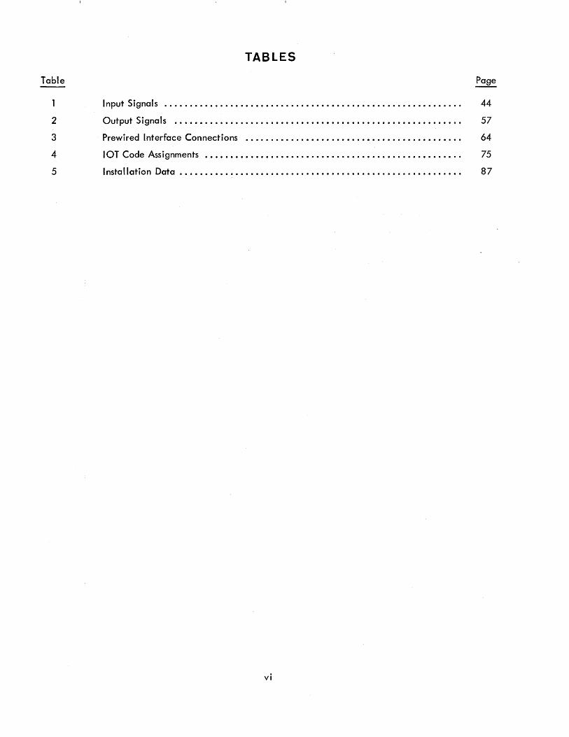
Programmed Data Transfer Interface Block Diagram •••.• '" •.•••••..•••••....•
Decoding of lOT Instructions •..•..•.•••••••••••••••••.•••.•••••••••••••••
Programmed Data Transfer Timing Diagram •..•••.•.••..•••..•••..•••.•..•.••
lOP Generator ••.••..••.•••.•••••••••••••••••••••.•••••..••.••..•••.•••
Generation of lOT Command Pulses by Device Selector ••••.•••••••••..•••••.•
Typical Device Selector (Device 34) •.••••.•.••••••••••••••••.•••••.•••••••
Slow Cycle Facility •.•••..•••.••••.•••••••.•••••••••••.••••.•••.••.•••..
Input/Output Skip Fac iI ity •..•.•.•.••.••••••••••••••.••.•••••..•••••.••.•
Information Collector and Information Distributor •••••••••••.••••.•••..••••••
Programmed Data Input Transfer ••.•..•.• " •.••••.•••.••••••••••••.••.••••...
Programmed Data Output Transfer ...•.•••••••.•.•••••••.•.••.......••••••.
Program Interrupt Facility ..•••.••.•••.••.••••••.••••••••••.•.•••••.•••.•.
Multiple Use of lOS and PI ...••.•.••.•...•••••...•••••••• " ••••••••••••••..
Programmed Data Input Flow Diagram ....•.••••..•.•••••.•••....•••••••.•..
Programmed Data Output Flow Diagram .••.•••.•..•.•.••.•••••••..•.••••••.•
Data Break Transfer Interface Block Diagram •••..••••••••••••••••••••••••.•.
Data Break Transfer Timing Diagram .•.....•••••..••. '" ••••••••••••.•••..•.
Data Break Fac iI ity I nterface of Computer .••..••••.•••••••••...••••....••••
Data Address Input Interface of Computer ••.•...•••.•.•••••.•..••••.••••.•.•
Data Information Input and Output Interface of Computer ...•••••••••••.••••..
Inverter Circuit •.....••••••••.•••.••••.•••••••.••••.•..••••.•..•..••.•••
Bus Driver Output Circuit .••..•..•..•••.•••••••••••••••.•••••••••...•.••.
Pulse Ampl ifier Output Circuit .•.•.••.•.••••.•..•.•••••••...••••••••••..•.
Diode Gate Circuit .••.•.•••••••.••••.••••.••••••••••••.•.•••••.•••.•.•.
Interface Cable Connector Locations and Assignments ••••••••••.•.••.••••....
Information Collector Channel Assignments ...•.••.•••...•..•••.•.•••••...••
Basic PDP-7 Component Locations ••.••.•..••••••.••.•••..••••.••••.••••.•.
Typical PDP-7 System Component Locations .••••••••••.•.•..••..••.••••••.•.
Basic PDP-7 Installation Dimensions •.•..••••••••....•..•..••.•...•...••..•
v
7
8
9
11
12
13
14
15
17
18
20
21
23
25
26
29
30
32
34
35
38
38
39
40
42
77
84
85
86
TABLES
Table Page
2
3
4
5
Input Signals .••••.•..••••••.•••••••••.••••••.•••••••.••..••..•...••.... 44
Output Signals ..••••.•••••••.•••••••.•.•.••••••••••.••.••••••••.•••••••
Prewired Interface Connections ••.•..•.•.•••••••••••••.••••••••••••••••.•.
lOT Code Assignments ••••••••••••••...••.••••••••••••.•.••....•••.•••••.
Installation Data ••.•••••••••••••••••.••...••••••••••••••••••••••.•••..••
vi
57
64
75
87


CHAPTER 1
INTRODUCTION
Since the processing power of a computer system depends, in large measure, upon the range and number
of peripheral devices that can be connected to it, the Programmed Data Processor-7 (PDP-7) has been
designed with a very broad, flexible, and expandable interface. This manual defines the interface char
acteristics of the computer to allow the reader to design and implement any electrical interfaces required
to connect devices to the PDP-7. This manual also provides information for planning the installation of
a PDP-7 system. Information in this manual applies only to PDP-7 systems with serial numbers above 100.
Refer to the PDP-7 Interface and Installation Manual, F-78, dated 1/66, for information on systems with
serial numbers below 100.
The PDP-7 is a digital machine designed for use as a general-purpose computer, an independent informa
tion handl ing faci I ity, or as the control element in a complex processing system. The PDP-7 is a single
address, fixed l8-bit word length, parallel processing binary computer using lis complement arithmetic
(2 1s complement arithmetic faci I itates mu I tiprec i sion operations). Cyc Ie time of the random-access core
memory is 1 .75 jJsec, permitting a computation rate of up to 285,714 additions per second.
Programming features of the computer include indirect addressing, microprogramming (combining instructions
to occur in one 1 .75~sec machine cycle), and programmed monitoring of peripheral devices. Real-time
features of the computer include program interrupt (entry into a subroutine caused by a request from an
I/O device), input/output skip facility (program flow modification as a function of the status of a selected
peripheral device), and high-speed data break channel (direct input/output access to computer core mem
ory for cycle-steal ing data transfers at a rate of over 10 mi Ilion bits per second). Eight autoindex registers
simplify sorting, searching, and multiple input/output list processing operations. An operator console pro
vides manual control and visual indication of programmed operations. An l8-bit switch register per
mits manual entry of data and instructions, or status information to be sensed by the program. The console
displays all active registers, including the memory address register, memory buffer register, accumulator,
link bit, machine state, instruction register, program counter register, and multiplier quotient register of
the optional extended arithmetic element.
The basic PDP-7 system consists of a Type KAl7 A Processor, a Type 149 Core Memory, and a Type KAl1 A TM
I/O Package composed of FLIP CHIP circuit modules and solid-state power supplies. These hybrid silicon
™ FLIP CHIP is a trademark of Digital Equipment Corporation, Maynard, Mass.

circuits have an operating temperature range exceeding the limits of 32° to 122°F, so no air-conditioning
is requ ired at the computer si te. Standard 115v, 60-cps power operates the computer. The basic system
is self-contained in a 3-bay cabinet 69-1/8 inches high and 61-3/4 inches wide. This unit weighs ap
proximately 1150 Ib, requiring no subflooring or bracing.
In addition to the standard tape reader, tape punch, and Teletype keyboard/re~ader, the PDP-7 system
can operate over 64 input/output devices. Existing interface designs permit connection of a number of
DEC options to the computer, including devices such as line printers, magnetic: tape transports, magnetic
drums, card equipment, analog-to-digital converters, CRT displays, and digitClI plotters. The PDP-7
system can also accept other types of instruments or hardware devices that have an appropriate interface.
The simple I/O techniques of the PDP-7 allow inexpensive, straight-forward device interfaces to be
real ized. Any device interface needs control to determine when an information exchange is to take place
and to specify the location(s} in the computer core memory which accept or yield data. Either the com
puter program or the transferring device may exercise this control. Transfers made under control of the
computer program are called programmed data transfers. Transfers made under control of the external
device are called data break transfers.
PROGRAMMED DATA TRANSFERS
The majority of I/O transfers occur under control of the computer program. The maximum real istic rate of
transferring 18-b it words is 33 kc in the program interrupt mode. Normally this speed is well beyond that
required for laboratory or process control instrumentation .. To transfer and stqre information under program
control requires about six times as much computer time as under data break control. In terms of real time,
the duration of a programmed transfer is rather small due to the high speed of the computer.
To real ize f~1I benefit of the built-in control features of the PDP-7 programmed I/O transfers should be
used in most cases. Controls for devices using programmed data transfers are usually simpler and less
expensive than controls for devices using data break transfers. Analog-to-digital converters, digital-to
analog converters, digital plotters, I ine printers, message switching equipment, and relay control systems
typify equipment using the programmed data transfer channels.
Using programmed data transfer channels, simultaneous operation of devices is llimited only by the relative
speed of the computer with respect to the device speeds, and the search time required to determine the
device requiring service. The percent of computer time taken for I/O servicin!~ is roughly:
%1/0 time = sum of device rates (in cps) x service time (fJsec per interrupt) x 10-4
For comparison, it takes less t-han 3% of computer running time to read or write conventional IBM
compatible magnetic tape at 556 bits per inch and 75 inches per second.
2

DATA BREAK TRANSFERS
Devices which operate at very high speed or which require very rapid response from the computer use the
data break transfer channel. This channel permits an external device, almost arbitrarily, to insert or ex
tract words from the computer core memory, bypassing all program control logic. Because the computer
program has no cogn izance of transfers made through this channel, programmed checks of input data are
made prior to use of information received in this manner.
The data break is particularly well-suited for devices that transfer large amounts of data in block form,
e. g., high-speed magnetic tape systems, high-speed drum memories, or CRT display systems containing
memory elements.
PERTINENT DOCUMENTS
The following publications serve as source material and complement the information in this manual.
1. Digital Logic Handbook, C-105. This book describes the functions and specifica
tions of FLIP CHIP modules and module accessories used in the PDP-7, control interfaces,
and peripheral devices.
2. PDP-7 Brochure, F-71. This leaflet presents the basic functions of the PDP-7
hardware, software, instructions, and standard optional equipment.
3. PDP-7 Users Handbook, F-75. This book contains computer organization in
formation, detailed information on the function of interface facilities, and de
scriptions of the timing and operations performed by all instructions.
4. PDP-7 Maintenance Manual, F-77 A. This manual gives functional descrip
tion, principles of equipment operation, interface, installation, operating
procedures, and detailed maintenance information for machines with serial numbers
above 100.
5. Instruction manuals for appropriate input/output device options used in PDP-7
systems are avai lable.
6. PDP-7 Price List, F-72. This leaflet contains current price information on the
basic computer, computer options, and standard input/output equipment.
3

LOGIC SYMBOLS
Figure 2 defines the symbols used to express digital logic circuits and signals in the illustrations of this
manual.
4
--{>
•
DEC STANDARD NEGATIVE PULSE
DEC STANDARD POSITIVE OR POSITIVE-GOING PULSE
DEC STANDARD NEGATIVE LEVEL
DEC STANDARD GROUND LEVEL
FLOW
-15V LOAD RESISTOR CLAMPED AT -?Iv
PNP TRANSISTOR INVERTER 1. EMITTER 2. BASE 3. COLLECTOR
LOGIC AND GATE FOR NEGATIVE SIGNALS WITH COMPLEMENTARY OUTPUT SIGNALS
LOGIC OR GATE FOR GROUND LEVEL SIGNALS WITH COMPLEMENTARY OUTPUT SIGNALS
LOGIC NAND GATE FOR NEGATIVE SIGNALS
DIODE-CAPACITOR-DIODE GATE 1. CONDITIONING LEVEL INPUT 2. TRIGGERING PULSE INPUT 3. PULSE OUTPUT
FLIP-FLOP (BISTABLE MULTIVIBRATOR) 1. GATED SET-TO-l INPUT 2. GATED CLEAR-TO-O INPUT 3. DIRECT CLEAR-TO-O INPUT 4,5 OUTPUTS
Figure 2 Logic Symbols
4

INVERTING BUS DRIVER
B OR W SERIES PULSE AMPLIFIER. OUTPUT CAN BE MADE POSITIVE OR NEGATIVE BY REVERSING GROUND AND SIGNAL OUTPUT TERMINALS
R SERIES PULSE AMPLIFIER. OUTPUT ALWAYS POSITIVE, REFERENCED TO -3V.
OPTIONAL DEVICE SELECTOR LOGIC AS USED FOR ONE SELECT CODE
Figure 2 Logic Symbols (continued)
5

CHAPTER 2
PROGRAMMED DATA TRANSFERS
The PDP-7 is a parallel-transfer machine that collects and distributes data in bytes of up to 18 bits.
Figure 3 shows information flow within the computer to effect a programmed data transfer with input/output
equipment.
BITS 0-3
MEMORY BUFFER
REGISTER (MB)
BITS 15-17
BITS 6-11
lOP PULSES . ..-------.
IOP GENERATOR
ACCUMULATOR REGISTER
(A C)
DEVICE SELECTOR
(OS)
IOT COMMAND PULSES
SLOW CYCLE REQUEST
Figure 3 Programmed Data Transfer Interface Block Diagram
CONNECTIONS TO INPUT I OUTPUT DEVICE
All programmed data transfers take place through the accumu lator, the 18-bit arithmetic reg ister of the
computer. The computer program controls the loading of information into the accumulator (AC) for an
output transfer, and for storing information in core memory from the AC for an input transfer. Information
in the AC for output transfer is power ampl ified and suppl ied to the bussed connections of many peripheral
devices by the information distributor (I D). Then the program-selected device can sample these signal
I ines to strobe AC data into a control or information register. Input data signals arrive from many periph
eral devices at input mixer circuits of the information collector (IC), which transfers data into the AC.
In the input/output skip facil ity (lOS), command pulses from the device selector (DS) sample the condition
of I/O device flags. The lOS allows branching of the program based on the condition or availability
7

of peripheral equipment, effectively making programmed decisions to continUE! the current program or
to jump to another part of the program, such as a subroutine that services an I/O device.
The DS generates command pulses during execution of input/output transfer (lOT) instructions. All in
structions stored in core memory as a program sequence are read into the memory buffer register (MB) to
be executed. The operation code in the four most significant bits (bits 0 through 3) of the instruction is
transferred into the instruction register (lR) and decoded to produce appropriate control signals. When
the operation code is recognized as an lOT instruction, the lOP generator produces time-sequenced lOP
pulsesasa function of the three least significant bits of the instruction (bits 15 through 17 in the MB). The
lOP pulses, with an I/O device selection code in bits 6 through 11 of the instruction, are suppl ied as bus
inputs to all gates of the DS. The gating circuits of the DS associated with a sp1ecific device are enabled
by the select code to regenerate lOPs as specific lOT command pulses. Figure.4 shows the decoding of an
lOT instruction and Figure 5 indicates the timing of the lOP and lOT pulses.
DEVICE CLEAR AC AT EVENT SELECTION TIME 1 IF BIT IS A 1
OPERATION CODE 70a = lOT INSTRUCTION
~ r-~ A
I :< I :< I :.: I :.: I >: I :.: I '---y-'
SUBDEVICE SELECTION
'---y-' "---y--' SUBDEVICE lOP PULSE SELECTION GENERATION
CONTROL
Figure 4 Decoding of lOT Instructions
One lOT instruction can generate one, two, or three sequential lOT pulses. These command pulses are des
ignated by the octal code of the twelve least significant bits of the instruction in which they are generated;
e.g., lOT 3401 (usually bits 4 and 5 are unused and are assumed to be O's unless. otherwise specified).
These lOT command pulses from the DS go to the lOS, the IC, and to a specific I/O device whose action
they control. In this manner, the program produces commands to transfer data into or out of I/O devices;
to cause the program to skip or not skip an instruction based on the condition of (In external device flag;
or to start, stop, or perform operations in devices controlled by a command pulse.
lOT instructions can use the normal computer cycle time of 1.75 Ilsec, or can occur in a slow cycle ad
justed to the speed of the slowest I/O device. The device selector can be wired to cause entry into a
slow cycle for any device, when its select code is in the lOT instruction being executed. Figure 5 shows
the timing of command pulses for devices using the normal or slow cycle and the availability of the AC
for transfers.
8

-0
COMPUTER TIME
TIMINr, PULSE GENERATOR COMPOSITE OUTPUT (70-NSEC PULSES}
GROUND
-3 VOLTS
I ANY lOT INSTRUCTION (FETCH) CYCLE I t (1.75 MICROSECONDS) "
I I I- 120 I I I I -l I 120 I I 150 -l i- I NSEC I 120 --I t- I 150,.-j r- i NSEC 120 ,....-+j l-
I NSEC I I I I NSEC I I I NSEC I I I I NSEC I I 1-240 ...., I 1---640 NSEC----J..- 270-l /+:210..!.-240,..../ 1---640 NSEC--I-270-l !.-210,..! I NSEC I I I I NSEC I I NSEC I NSEC I I I NSEC I I NSEC I
T6 T7 TI T2 13 T4 T5 T6 T7 T1 T2 13 T4 T5 T6 I I J I I I I I I I I J J J J
T7 T3 T4 T5 T6 T7 TI T2 13 T4 T5 T6
MEfv'f)RY BUFFER REGIS TE R OUTPUT
NOT AVAILABLE ~~25 NSEC AVAILABLE
ACCUMULATOR DATA FOR OUTPUT TRANSFER
ACCUMULATOR CLEARED FOR DATA INPUT TRANSFER IF MB 14 CONTAINS A 1
r' lOP GENERATOR OUTPUT IOP 2 (400-NSEC PULSES)
IOP4
NOT READY ~_T6+100 NSEC I-T4+20 NSFC READY
NOT READY
READY
GROUND
-3 VOLTS
GROUND
-3 VOLTS
GROUND
-3 VOLTS
T4+IOONSEC--+IL ______________________________________ ~
T5 + 20 NSEC--+ .... ! ________ -'
T7+20 NSEC-.... ! ________ -'
TI + 20 NSEC OF NE X T C YC L E -!'--______ ---'
rIOT XXOI GROUND
t -3 VOLTS
T5+40 NSEC-!~ ______ --,
OPTIONAL DEVICE SELECTOR OUTPUT (400-NSEC PULSES)
lOT XX02 GROUND T7+ 40 NSEC-! .... ________ -'
-3 VOLTS
lOT XX09 GROUND -3 VOLTS
TI + 40 NSEC OF NEXT CYCLE--+ .... ! _______ -'
COMPUTER TIME
TIMING PULSE GENERATOR COMPOSITE OUTPUT (70-NSEC PULSES)
MEMORY BUFFER REGISTER OUTPUT
ACr.uMULATOR DATA FnR OUTPUT TRANSFER
ACCUMULATOR CLEARED FOR DATA INPUT TRANSFER IF MBI4 CONTAINS A 1
rop GENERATOR COMPOSITE OU' PUT (400-NSEC PULSES)
OPTIONAL DEVICE SELECTOR COMPOSITE OUTPUT 1400-NSEC PULSES)
(0) NORMAL CYCLE
ANY lOT INTRUCTION (FETCH) CYCLE _I I -- --- (1.36 MICROSECONDS+2 PRESET PERIODS) I -J I.- 210
I 150 J I I 120 I I I I I I 120 I I 120 I NSEC I NSEC I-- 120 NSEC-+j ~ I I -+j r-NSEC I -+j I"-NSEC I
1 I..., j4-NSEC I I 1 I PRESET ACCORDING TO SLOWEST I PRESET ACCORDING TO SLOWEST I I I 1 1 I 1-240~ I 1----640 NSEC~270 -I I'-;~0--r-- I/O DEVICE,! MICROSECOND ~ 110 DEVICE,I MICROSECOND ----! r----640 NSEC~N2;E~""" 1 I
T6 NSEC T7 Tl T2 13 NSEC T4 T5 N EC T6 MINIMUM T7 MINIMUM TI T2 13 T4 T5 T6
J I J J J J I J I I I I I I I
GROUND
-3 VOLTS T6 T7 TI T2 T3 T4 T5 T6 T7 TI T2 73 T4 T5
NOT AVA/LABI E ~325 NSEC AVA/LABL E
NOT REACT' ~ T6+ 100 NSEC I-T4 .,...'0 NSEC REAc~r
NOT READY T4+ tOO NSEC=-:;j READY '--------------------------------------------------------------------------------'
GROUND I -3 VOLTS T5 +20 NSEc-1 T7+ 20 NSEC-! T1+20 NSEC---I
lOP I lOP 2 OF NEXT CYCLE rop 4
_:~~~~ T5+40 NSEC-I T7+40 NSEC-I TI+40 NSEC--I r IOT XXOI IOT XX02 OF NEXT CYCLE IOT XX04
( b) SLOW CYCLE
Figure 5 Programmed Data Transfer Timing Diagram

Devices which require immediate service from the computer program, or which take considerable computer
time to discontinue the main program until transfer needs are met, can use the program interrupt (PI) fac il ity.
In this mode of operation, the computer can initiate operation of I/o equipmEmt and continue the main
program until the device requests servicing. A signal input to the PI requestinH a program interrupt causes
storing of the conditions of the main program and initiates a subroutine to service the device. At the con
clusion of this subroutine, the main program is reinstated until another interrupt request occurs.
TIMING CYCLE
Cycle time of an lOT instruction is either normal or slow, depending upon the device addressed (see
Figure 5). All devices use the normal cycle unless the device selector for the selected equipment is wired
to request a slow cycle.
The normal lOT cycle time is 1 .75 fJsec, or equal to a normal computer cycle. At computer time 5 (T5)
10Pl is produced, at time 7 (T7) IOP2 is produced, and at time 1 (Tl) of the next cycle IOP4 is produced.
Time 1 of the next cycle can be used for IOP4, since time 1 is normally used only to prepare to read the
next instruction into the MB from core memory; so the IR and MB still contain the same information. The
time from the start of 10Pl to the start of IOP2 is 450 nseci from the start of IOP2 to IOP4 is 150 nsec.
If consecutive lOT instructions occur, the time from the start of IOP4 in the first instruction to the start
of IOP1 of the second instruction is 1 • 15 fJsec.
The slow lOT cycle time produces lOP pulses at the same computer times as during a normal cycle; however,
the delay between timing pulses is adjustable from a 1 fJsec to 4 fJsec. Under special conditions modifi
cations to the delay modules can produce even longer time delays. In all cases, delays are set to ac
commodate the slowest device using the slow cycle feature of the computer (this timing exists for all devices
requesting a slow cycle). A complete slow cycle requires a 3.36 fJsec minimum.
lOP GENERATOR
The logic circuits of the lOP generator are shown in Figure 6. When the instruction register decoder
detects an lOT instruction (the operation code in bits MBO-MBS = 111 °2
), it generates the lOT signal.
The lOT signal conditions one input of each of the three gates that trigger pulse ampl ifiers to produce
the lOP pulses. Each 3-input NAN D gate is operated by the condition of a bil" in the lOT instruction
and a computer timing pulse, to produce one of the sequential lOP pulses. Eac:h lOP pulse goes to one
gate of all device selector channels to allow generation of an lOT command pulse at one of the three se
quential event times within the instruction. Figure 6 shows the computer timinH pulses and instruction bit
conditions which generate each lOP pulse for the three event times.
10

EVENT TIME I
EVENT TIME 2
EVENT TIME 3
Figure 6 lOP Generator
DEVICE SELECTOR (DS)
The DS selects an I/O device or subdevice according to the address code of the device specified in bits 4
through 13 of the lOT instruction. Selection of the device can request a slow cycle. The DS then gener
ates lOT command pulses for each lOP pulse received, and transmits these commands to the 105, the IC,
and/or the device . Generally, lOT command pulses are used as follows:
Command
lOT XX01
lOT XX02
lOT XX04
Use
Applied to the 105 to sense the condition of the device flag.
Appl ied to the IC to transfer data into the computer I or appl ied to the device to initiate a data transfer from the computer and clear device flags.
Appl ied to the device to initiate some operation (start, read, etc.).
11

Each group of these command pulses requires one channel of the DS, and each channel requires a different
address {or select code}. One device can, therefore, use several channels of the DS. Figure 7 shows
generation of command pulses by several channels of the DS.
lOP 1 lOP2
lOP 4
MBBS
MBS7
MSSS
MBB9
MBSIO
MBS11
Figure 7 Generation of lOT Command Pulses by Device Selector
}
COMMAND PULSES TO DEVICE 34
,/
I I I I I I I J
BUSSED INPUT TO ALL DEVICE SELECTORS
The logical representation for a typical channel of the DS, using channel 34, is shown in Figure 8. A
6-input NAND gate wired to receive the appropriate signal outputs from MB6-11 for select code 34 acti
vates the channel. In the DS module, the NAND gate contains 14 diode input terminals; 12 of these con
nect to the complementary outputs of MB6-11, cmd 2 are open to receive subdevice or control condition.
signals as needed. Either the 1 or the 0 signal f~om each MB bit is disconnected by removing the appro
priate diode from the NAND gate when establishing the select code. The ground level output of the
NAND gate indicates when the lOT instruction selects the device, and can therefore request a slow cycle
12

for the device. This output also enables three gating inverters, allowing them "to trigger a pulse ampl ifier
if an lOP pulse occurs. The positive output from each pulse amplifier is an lOT command pulse identified
by the select code and the number of the initiating lOP pulse. Three inverters receive the positive lOT
pulses to produce complementary lOT output pulses. A pulse ampl ifier modu Ie can be connected in each
channel of the DS to provide greater output drive or to produce pulses of a specific duration required by
the selected device.
Figure 8 Typical Device Selector (Device 34)
SLOW CYCLE FACILITY
Up to twelve devices can request a slow lOT cycle by connecting the ground-level select signal output
of the DS channel to the slow cycle request facility. This facility consists of a 12-input diode NOR gate
for ground levels as shown in Figure 9. None of the basic PDP-7 input/output devices require a slow
cycle.
13

LEVELS FROM DEVICE SELECTOR TO REQUEST SLOW CYCLE FOR UP TO 12 DEVICES
Figure 9 Slow Cycle Facility
INPUT/OUTPUT SKIP (lOS)
The condition of an I/O device flag and generation of an lOT pulse combine in the lOS to cause the program
to skip over one instruction. Incrementing the program count without executing the instruction at the current
program count causes skipping. The lOS facil ity consists of multiple 2-input ANID gates with outputs con
nected in parallel to allow any gate to trigger the pulse ampl ifier which producc~s the 10 SKIP pulse. A
flag or status level from the device and an lOT XX01 pulse from the appropriate channel of the DS provide
input connections to each gate as shown in Figure 10. In this manner an lOT instruction can check the
status of an I/O device and skip the next instruction if the device requires servicing. Programmed testing
in this manner allows the routine to jump out of a sequence to a subroutine that services the device tested.
Assuming that a device is already operating, a possible program sequence to test its availability follows:
Address
100, 101, 102,
Instruction
703401 600100 10XXXX
Remarks
/SKIP IF DEVICE 34 IS READY /JUMP .-1 /ENTER SERVICE ROUTINE FOR DEVICE 34
14

Figure 10 Input/Output Skip Facility
15

When the program reaches address 100, it executes an instruction skip with 7034m. The skip occurs only
if device 34 is ready when the lOT 3401 command is given. If device 34 is not ready, the flag signal
disqual ifies the 105 gate, and the skip does no1" occur. Therefore, the program continues to the next in
struction which is a jump back to the skip instruction. In this example, the program stays in this waiting
loop until the device is ready to transfer data, at which time the gate in the 105 is enabled and the skip
occurs. When the skip occurs, the instruction in location 102 transfers program control to a subroutine
to service device 34. This subroutine can load the AC with data and transfer it to device 34, or can load
the AC from a register in device 34 and store it in some known core memory address.
INFORMATION COLLECTOR (lC)
The information collector is a 7-channel gated Input mixer that transfers bytes of up to 18 bits into the AC
from signals suppl ied by an external device. Each channel consists of 18 2-input diode AND gates, trig
gered by a common lOT command pulse from the DS. (Usually the lOT instruction that strobes information
into the AC via the IC is microprogrammed with bit 14 containing a 1.so that the:! AC is cleared at event
time 1 ~) Figure 11 shows the IC logic circuit configuration.
The perforated tape reader and I/O status bits each occupy one l8-bit IC channel. The teleprinter occu
pies eight bits of a third channel. The remaining four and one-half channels are available for connection
to any peripheral and optional input equipment. Each PDP-7 input option connects directly into one or
more channels of the IC. For operation of more than seven input devices, the Ie is easily expandable in
blocks of seven channels to accommodate any number of channels.
INFORMATION DISTRIBUTOR (lD)
The I D is an output bus system that transfers information from the AC to external devices. Accumulator
output signals are buffered by 18 bus driver circuits and driven through cables to the I/O package. The
ID in the I/O package contains nine la-bit connection points, or channels, for each bussed signal; one
channel receives bussed connections from the processor, seven channels are avaiiable for individual de
vice cable connections, and one channel is for external expansion of the ID. (The paper tape punch and
teleprinter receive AC output signals directly from the bus drivers and do not require connection through
the ID.) If all seven channels are used, the ID can be expanded to any number ()f output channels by
adding suitable non-inverting buffering and distribution channels similar to the sfandard I D.
16

'J INFORMATION DISTRIBUTOR IN I/O PACKAGE
Figure 11
ONE PAIR at;.RIPS TERMINAfx~ANSION
::l FOR 10 TER .... At
'). ~VEN PAIRS :VICE ~ -- STRIPS [g~NECTIONS RMINAL STRIPS
7 ............ ~ CABLE __ ?NN~/6~~C~~G?~g~E~:O~~~~~ /" U ),. ~ CONNECTIONS D)
Information Collector and Information Distributor
REGISTER
Figure 12 Programmed Data Input Transfer
DATA TRANSFERS INTO THE PDP-7
I I
POP-7
1
EXTERNAL DEVICE
lOT XX02 and lOT XX04 command pulses control an external input device as indicated in Figure 12.
When ready to transfer data into the PDP-7 accumulator, the device sets a flag connected to the lOS.
The program senses the ready status of the flag and issues an lOT instruction to read the contents of the
external device buffer register into the AC. Usually this instruction contains a clear AC command and an
lOT XX02 (lOT XX12) to effect the transfer. If the AC is not cleared before the transfer, the resultant
word in the AC is the inclusive OR of the previous word in the AC and the word lrransferred from the de
vice buffer register. To clear the AC prior to the transfer, bit 14 of the lOT instruction should contain
a 1. This microprogramming clears the AC at event time 1 (computer time T5), and an lOT XX12 pulse
causes the transfer to occur at event time 2 (computer time T7).
18
Following the transfer (possibly in the same instruction) the program issues an lOT XX04 command pulse
to initiate further operation of the device. This pulse also clears the device flag. For simpl icity, the
transfer path in Figure 12 shows only a single channel of the IC gates.
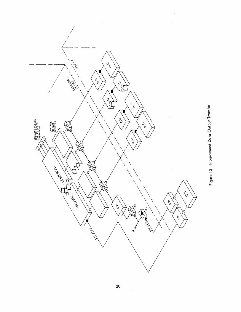
DATA TRANSFERS OUT OF THE PDP-7
lOT XX02 and lOT XX04 command pulses control an external output device as indicated in Figure 13.
The AC is loaded with a word (e. g., by a LAC instruction); then the lOT instruction is issued to transfer
the word into the control or data register of the device by an lOT XX02 pulse, and operation of the device
is initiated by an lOT XX04 pulse. The word transferred in this manner can be a character to be operated
upon, or can be a control word sampled by a status register to establish a control mode.
Connecting an output device to the PDP-7 interface adds at least three commands to the instruction rep
ertoire. These commands use an lOT XX01 pulse to skip ·on the ready condition of the device flag, an
lOT XX02 pulse to effect a transfer from the AC to the device, and an lOT XX04 pulse to initiate opera
tion of the device.
PROGRAM INTERRUPT (PI)
When a large amount of computing is required, the computer should process data rather than simply wait
for an I/O device to become ready to transfer data. The PI faci! ity, when enabled by the program, re-
I ieves the main program of the need for repeated flag checks by allowing I/O device ready flags to auto
matically cause a program interrupt break. At the break location, program control transfers to a subroutine
which determines the requesting device and initiates an appropriate service routine.
The basic PI faci! ity can accommodate interrupt requests from nine devices and is expandable. As shown
in Figure 14, the PI facility receives a negative signal from the flag of a device to request an interrupt.
This flag signal input to the PI can also connect to the 105 facility to allow the program interrupt sub
routine to detect the device requesting the interrupt if multiple devices are connected to the PI. On
Figure 14, note that any fI ip-flop or flag signal connected to an input of any of the six 3-input NOR
gates of the I/O package triggers the interrupt control circuits of the processor to cause a program inter
rupt break, (if a break is not already in progress and if the interrupt system is enabl ed).
19
/ /
\-~--
/
20
..... :> 0.. ..... :> o o ..... o o
-0 <D E E o '-0> o '
Q..
<D ':> 0> u:

EXTERNAL DEVICE
COMPUTER PROGRAM rNTERRUPT FACILITY
I
COMPUTER 110 SKIP FACILITY
Figure 14 Program Interrupt Facility
NO BREAK STARTED
PROGRAM INTERRUPT FACILITY ENABLED
If only one device is connected to the PI facil ity I program control can be transferred directly to a routine
that services the device when an interrupt occurs. This operation occurs as follows:
21
SR
Address
1000 1001 1002
0000
0001 2000
3001 3002 3003 1003 1004
Instruction Remarks
/MAIN PROGRAM /MAIN PROGRAM CONTINUES /INTERRUPT REQUEST OCCURS
I NTERRUPT OCCURS /LlNK, EXTEND AND TRAP FLIP-FLOP STATES, /EXTENDED PROGRAM COUNT, / AND PROGRAM COUNT (PC==1003) / ARE STORED IN 0000
JMP SR /ENTER SERVICE ROUTINE /SERVICE SUBROUTINE FOR /INTERRUPTING DEVICE AND SEQUENCE TO RESTORE /AC, AND RESTORE LAND EPC IF REQUIRED
ION /TURN ON INTERRUPT JMP I 0000 /RETURN TO MAl N PROGRAM
/MAIN PROGRAM CONTINUES
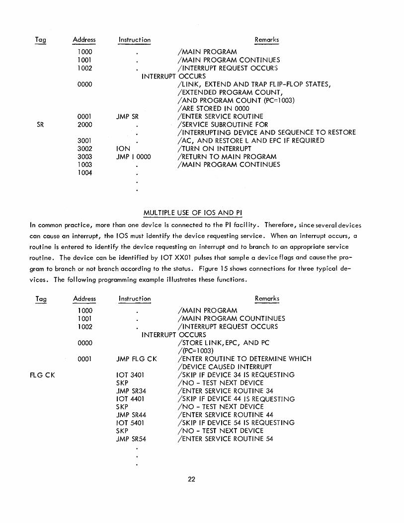
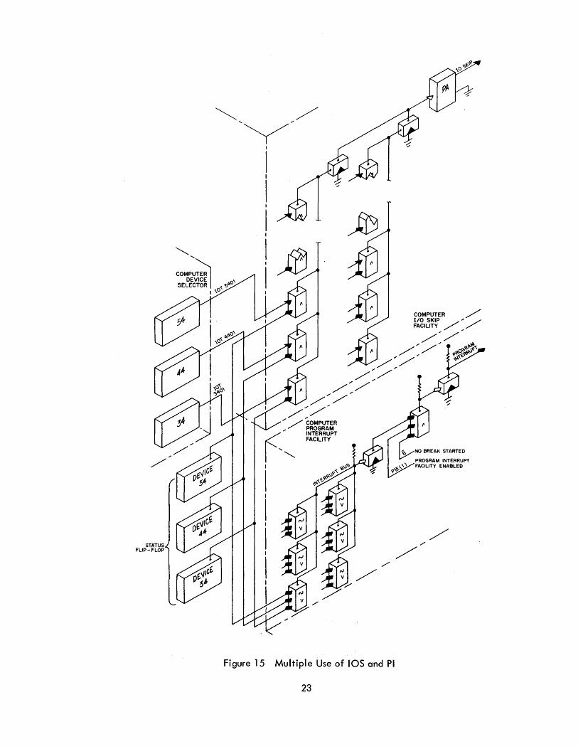
MULTIPLE USE OF lOS AND PI
In common practice, more than one device is connected to the PI faci I ity. Therefore, since several devices
can cause an interrupt, the lOS must identify the device requesfing service. When an interrupt occurs, a
routine is entered to identify the device requesting an interrupt and to branch tel an appropriate service
routine. The device can be identified by lOT XXOl pulses that sample a device flags and causethe pro
gram to branch or not branch according to the status. Figure 15 shows connecti()ns for three typical de
vices. The following programming example illustrates these functions.
FLG CK
Address
1000 1001 1002
0000
0001
Instruction Remarks
/MAIN PROGRAM /MAIN PROGRAM COUNTINUES /INTERRUPT REQUEST OCCURS
I NTERRUPT OCCURS
JMP FLG CK
lOT 3401 SKP JMP SR34 lOT 4401 SKP JMP SR44 lOT 5401 SKP JMP SR54
/STORE LINK, EPC, AND PC /(PC=1003) /ENTER ROUTINE TO DETERMINE WHICH /DEVICE CAUSED INTERRUPT /SKIP IF DEVICE 34 IS REQUESTING /NO - TEST NEXT DEVICE /ENTER SERVICE ROUTINE 34 /SKIP IF DEVICE 44 IS REQUESTING /NO - TEST NEXT DEVICE /ENTER SERVICE ROUTINE 44 /SKIP IF DEVICE 54 IS REQUESTING /NO - TEST NEXT DEVICE /ENTER SERVICE ROUTINE 54
22
COMPUTER / 110 SKIP './ FACILITY /,"'-
'/ /, ~ ./' / ~Of:3~~~
".- , ~i('i-~-:' '/ ~' /, '/ /,
" / /, "/ /" "/ /"
" ./ COMPUTER ,,"'- PROGRAM
(
INTERRUPT FACILITY
'''-... I
I
I I
I I
I I
I
Figure 15 Multiple Use of lOS and PI
23
".-
/

Assume that the device that caused the interrupt is an input device (e. g., tape reader). The following example of a device service routine might apply:
Tag
SR
Instruction
DAC TEMP lOT XX12 DAC I 10 ISZ COUNT SKP JMP END
LAC TEMP ION JMPIO
Remarks
/SAVE AC /TRANSFER DATA FROM DEVICE BUFFER TO AC /STORE IN MEMORY LIST /CHEC K FOR END /NOT END /END. JUMP TO ROUTINE TO HANDLE END OF /L1ST CONDITION
/RESTORE LAND EPC IF REQUIIRED /RELOAD AC /TURN ON INTERRUPT /RETURN TO PROGRAM
If the device that caused the interrupt was essentially an output device (receiving data from computer),
the lOT - then - DAC I 10 sequence might be replaced by a LAC I 10 - then - lOT sequence.
EXAMPLE OF PROGRAMMED DATA INPUT AND OUTPUT
The following example, explaining the function and connections of the Teletype unit and Type 649B
Teletype control, summarizes interfacing a device with programmed input and output data transfers, using
both program interrupt and I/O sk ip fac it ities. Figure 16 shows the sequence of operations for a transfer
into the computer from the keyboard, and Figure 17 shows the sequence for printing information transferred
out of the computer.
Assume that a program is in progress and the keyboard of the Teletype is manuall)' operated to send infor
mation into the computer. When the key is struck, the control generates the 8-bit character and shifts
it into a keyboard buffer one bit at a time. When the character is complete in the register, the keyboard
flag is set to request a program interrupt. If the program interrupt is enabled (mean ing the program in
operation can be interrupted), when the flag is rclised a break occurs at the conclusion of the instruction
in progress. During the break cycle the contents of the link, trap mode bit, extended program counter
(EPC), and the program counter are stored at core memory address 000000, and the next instruction is
taken from address 000001 .
This instruction is usually a jump to an interrupt routine which checks the status of flags for all equipment
connected into the system. When this routine issues lOT instruction 700301, the 1 status of the keyboard
flag is identified and program control jumps to a subroutine that services the keyboard. This subroutine
. (assuming that the Land EPC need not be restored before returning to the main prc)gram) could consist of
the following:
24

OPERATING PROGRAM
BREAK REQUEST
BREAK GRANTED
(PROGRAM INTERRUPT DISABLED TO PREVENT OTHER INTERRUPTS FROM OCCURRING UNTIL THIS INTERRUPT IS COMPLETED)
CONTINUE PROGRAM
T
KEYBOARD OPERATIONS
AND SUBROUTINES
I I I
~
Figure 16 Programmed Data Input Flow Diagram
25
-~~--

OPERATING PROGRAM
BREAK REQUEST
BREAK GRANTED
INITIALIZING COMMAND
CONTINUE PROGRAM
T
TELEPRINTER OPERATIONS
AND SUBROUTINES
CLEAR TELEPRINTER
FLAG
I
~ I
Figure 17 Programmed Data Output Flow Diagram
26

Octal
700312-
06XXXX
20XXXX 700042 620000
Mnemonic
KRB
DAC I STORE
LAC AC SAVE ION JMPIO
Remarks
/CLEAR AC, THEN LOAD AC FROM CONTENTS /OF KEYBOARD BUFFER, AND CLEAR KEYBOARD /FLAG /WRITE CHARACTER AT ADDRESS CONTAINED /IN AUTOINDEX REGISTER IISTOREII /RESTORE AC FROM LOCATION IIAC SAVEll /ENABLE INTERRUPT SYSTEM FOR NEXT CHARACTER /RETURN TO MAIN PROGRAM FROM ADDRESS /STORED IN 00000 WHEN BREAK WAS STARTED
Upon completion of this subroutine the main program continues and the keyboard awaits the next manual
key operation.
Assume that the main program has accumulated and stored data in core memory, and that the data is to
be printed by the Teletype while the main program conti~ues. When the program recognizes the need to
print, it initial izes a print subroutine (by setting an autoindex register equal to the core memory address -1
for the dater, establ ishing a check for the last character to be printed, initial izing a counter to track the
number of characters printed, etc.) and then enters the print subroutine to print the first character. The
basic print subroutine might be similar to the following:
Octal Mnemonic
22XXXX LAC I 10
44XXXX ISZ COUNT 741000 SKP 60XXXX JMP END 700406 TLS
700042 ION
620000 JMPIO
Remarks
/LOAD CHARACTER INTO AC FROM ADDRESS /SPECIFIED BY AUTOINDEX REGISTER 10 /COUNT CHARACTERS /NOT LAST CHARACTER /LAST CHARACTER /TRANSFER CHARACTER FROM AC INTO PRINTER /BUFFER, CLEAR PRINTER FLAG, AND INITIATE /PRINTING /RESTORE LAND/OR EPC IF NECESSARY, THEN AC /ENABLE INTERRUPT SYSTEM FOR NEXT CHARACTER /BREAK /RETURN TO MAIN PROGRAM FROM ADDRESS /STORED IN ADDRESS 000000
Exit from this subroutine reestabl ishes the main program which now continues until interrupted by a pro
gram break. Having been initiated by the subroutine, mechanical printing of the first character continues
until complete, then raises the print flag. The print flag in the 1 state indicates that the teleprinter has
printed the last character and is ready to receive another character, and requests a program interrupt. If
the interrupt system is enabled, at the end of the current instruction the break state is entered to store the
contents of the L, EPC, and PC in address 000000. The next instruction is then taken from address 000001,
and program control is transferred to the interrupt routine. The program interrupt routine, as described
27

previously for the keyboard, senses the status of flags for all devices connected to the interrupt facility
until it determines the device requesting serViCE!. When the TSF instruction is given (lOT 700401) to skip
on the ready status of the printer flag, the print subroutine is again entered to load and print the next
character. At exit from the subroutine the main program is reentered from the point of the program break.
If the main program is an arithmetic routine that uses the I ink or a routine using extended memory, the
AC, L, and EPC must be restored by the device service routine prior to issuing the ION instruction. Res
toration of the L is accompl ished by an instruction sequence such as:
Octal
200000 740010
Mnemonic
LAC 0 RAL
Remarks
/LOAD WORD CONTAINING L /ROTATE TO RESTORE L
Restoration of the EPC is described in the PDP-7 Users Handbook, F-75, under the description of the
Type 148 Memory Extension Control. The AC should always be restored by the :service routine.
28

CHAPTER 3
DATA BREAK TRANSFERS
The data break facility allows one I/O device to transfer information directly with the PDP-7 core memory
on a cycle-stealing basis. Up to four dbvices can connect to the data break facility through the optional
Type 173 Data Interrupt Multiplexer.
Data break information transfers occur directly between the computer MB and a data register of the device,
and therefore do not affect the arithmetic or program control elements of the PDP-7. Transfer rates of up
to 571,000 words per second, or over 10 million bits per second, can be realized through this independent
data handling channel.
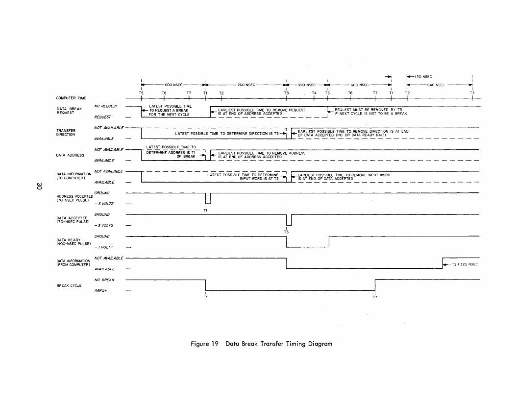
Figure 18 shows information flow to effect a data break transfer with an I/o device. Figure 19 indicates
timing requirements for input and output control and data signals, and the availability of register data
signals.
MEMORY ADDRESS REGISTER
(MA)
MEMORY BUFFER
REGISTER (MB)
DATA BREAK
FACILITY
DATA ADDRESS (15)
DATA INFORMATION (18 BITS IN)
DATA INFORMATION (18 BITS OUT)
ADDRESS ACCEPTED .. ... DATA ACCEPTED .. ... DATA READY ..
DATA BREAK ... REQUEST
:-" TRANSFER .... DIRECTION (IN) ~
CONNECTIONS TO INPUT I OUTPUT DEVICE
Figure 18 Data Break Transfer Interface Block Diagram
External devices requesting storage or retrieval access to core memory supply the following signals to
the computer:
DATA BREAK REQUEST
TRANSFER DIRECTION
DATA ADDRESS (15 bits)
DATA INFORMATION (18 bits)
- 3v for assertion
- 3v for into PDP-7, ground for out
- 3v for 1, ground for 0
- 3v for 1, ground for 0
29
w o
COMPUTER TIME
DATA BREAK REQUEST
TRANSFER DIRECTION
DATA ADDRESS
NO REQUEST
REQUEST
NOT AVAILABLE
AVAILABLE
NOT AVAILABLE
AVAILABLE
~ 1.-,20 NSEC I ,
,- 600 NSEC .'1 760 NSEC a,. 390 NSEC .,. 600 NSEC al "--640 NSEC a, , I " I I ,
T5 T6 T7 Tl T2 T3 T4 T5 T6 T7 TI T2 T3 L _____ I _ I 1 I I I I I " , - --T I -~ -- - --- ----.- -- - -------,-- -,-- ---T
LATEST POSSIBLE TIME TO REQUEST A BREAK EARLIEST POSSIBLE TIME TO REMOVE REQUEST REQUEST MUST BE REMOvED BY T5 FOR THE NEXT CYCLE '.:...:'T~N~F ~DRES~ACCEP~D _____ -.J IF NEXT CYCLE IS NOT TO BE A BREAK
----------------, LATEST POSSIBLE TIME TO DETERMINE DIRECTION IS T3
EARLIEST POSSIBLE TIME TO REMOVE DIRECTION IS AT END OF DATA ACCEPTED (IN) OR DATA READY (OUT) ~ ____________________________________ ~L ______________________ _
LATEST POSSIBLE TIME TO
DETERMINE ADDRESS iSTI- ., OF BREAK
EARLIEST POSSIBLE TIME TO REMOVE ADDRESS IS AT END OF ADDRESS ACCEPTED
NOTAVAILABLE ---,- - - - - - - - - - - - - - - - - - -, i DATA INFORMATION I LATEST POSSiBLE TiME TO DETERMINE --, tEARLIEST POSSIBLE TIME TO REMOVE INPUT WORD (TO COMPUTER) INPUT WORD IS AT T3 IS AT END OF DATA ACCEPTED
AVAILABLE ------------
GROUND ADDRESS ACCEPTED (70-NSEC PULSE)
DATA ACCEPTED (70-NSEC PULSE)
DATA READY (400-NSEC PULSE)
-3 VOLTS
GROUND
-3 VOLTS
GROUND
-3 VOLTS
u I
TI
u I
T3
NOT AVAILABLE . -DATA INFORMATION !== (FROM COMPUTER) T2+325 NSEC
AVAILABLE
NO BREAK
BREAK CYCLE
BREAK I
TI
Figure 19 Data Break Transfer Timing Diagram
I T7

The computer provides the following signals to the device using the data break facility:
ADDRESS ACCEPTED
DATA ACCEPTED
DATA READY
DATA INFORMATION (18 bits)
Standard DEC 70-nsec negative pulse when
device-supplied address is strobed into MA.
Standard DEC 70-nsec negative pulse when'
device-supplied information is strobed into MB.
Standard DEC 400-nsec negative pu Ise when
information is avai lable in MB for strobing
by external device. The external device can
use this pulse to strobe the MB information into
its register either directly or (when gate set-up
time is required) after a delay of up to 1 !-,sec.
- 3v for 1, ground for 0
DATA BREAK FACILITY
The data break facility controls entry into the break state to execute a data break, and produces the
pulses that strobe address and data into the computer and indicate data is ready to be strobed out of the
computer. Figure 20 shows the interface circuits of the data break facility.
Data break requests are synchronized with the computer timing cycle and the execution of instructions
by a DATA SYNC flip-flop. The T5-DlY pulse (T5 delayed 50 nsec) sets this flip-flop if the DATA
BREAK REQUEST (or DATA RQ) signal level is at - 3v (making a request), or clears it if the request is
not made (signal level is at ground). When set, the DATA SYNC flip-flop causes generation of a BK RQ
(or BREAK REQUEST) signal level that establishes the break state for the next cycle if the current cycle
completes an instruction. Therefore, to initiate a data break the DATA BREAK RE QUEST signal must be
present (negative) at the time the T5-Dl Y pulse occurs during the cycle immediately preceding the break.
Similarly, when the break is granted the DATA BREAK REQUEST signal must be removed (ground or open)
by the time the T5-DlY pulse occurs or the next cycle will also be a break state.
Note that a break state (but not a data break) can also be caused by a program interrupt (PROG SYNC (1)
signal) or by the real-time clock (ClK SYNC (1) signal).
The 1 status of the DATA SYNC flip-flop combines with the break condition of the major state generator
to produce a DATA. B signal level that enables generation of the ADDRESS ACCEPTED (or ADDR ACC),
DATA ACCEPTED (or DATA ACC), and DATA READY (or DATA RDY) pulses.
31

Figure 20 Data Break Foci lity Interface of Computer
32

The 70-nsec negative ADDRESS ACCEPTED pu Ise occurs at T1 time of all data break cyc les to strobe the
15 device-supplied DATA ADDRESS signals into the computer MAand EMA (extended MA) registers.
This pulse, available at the interface, can be used by the device to remove the DATA BREAK REQUEST
signal or to clear or change the data register in preparation for the next cycle.
The 70-nsec negative DATA ACCEPTED pulse occurs at T3 time of the data break cycle if the device
supplied TRANSFER DIRECTI'ON signal level is at - 3v to specify a data direction into the computer.
This pulse strobes the 18'devic,e-supplied DATA INFORMATION signals into the MB and is available at
the interface for use by the device to clear and/or change the data buffer register for the next cycle.
The direction of a dat<:J break transfer is always ,stated with respect to the computer. The TRANSFER
DIRECTION signal should be - 3v to specify a tra'n'sferinto the PDP-7, or should be ground to specify
a transfer out of the PDP-7. This signal should be presen~(:1t th~ time the data break request is mode;
however, it need not be present unti I T3 of the break cy<;:I,e.'
The 400-nsec negative DATA READY pulse occurs at T3time of all data break cycles. This pulse is not
used in the computer but is produced for the device to u,se directly, or delayed to allow for gate setup
time, to strobe the 18 computer DATA INFORMATION signals into its data buffer register.
DATA ADDRESS
Fifteen DATA ADDRESS (or DA) signals are recieved from the external device to specify the core memory
address to be used for the data break transfer. These signals are - 3v to signify a binary 1. They shou Id
be present when the data break request is made, but may be delayed if they are settled prior to T1 time
of the break cycle. These sign~ls'are received by'a2-input NAND gate at the 1 input of each MA flip
flop and extended MA flip-flop. Since the MA contains 13 bits, the flip-flops are designated MAS through
MA17. The two extension fl ip-flops are added to the IT,Iost significant end of the register and are de
signated EMA3 and EMA4. Each of these flip-flops is loaded with the information on the DATA ADDRESS
lines suppl ied by the device when the ADDRESS ACCEPTED pu Ise occurs. The data break fac iI ity gen
erates the ADDRESS ACCEPTED pulse at T1 time of a break cycle caused by a negative DATA BREAK
REQUEST signal. Figure 21 shows this data address interface logic of the computer.
DATA INFORMATION INPUT AND OUTPUT
Input data from an external device is received by the MB during a data break as 18 DATA INFORMATION
(or DI) signal levels. The DATA INFORMATION input signals should be present when the data break
request is made, but can be delayed if they are settled prior to T3 time of the break cycle. Each - 3v
signal (binary 1) enables a 2-input NAND gate at the 1 input of an MB flip-flop. The DATA ACCEPTED
33

pulse strobes all these gates. This pulse is generated in the data break facility at T3 of the break cycle
by negative DATA BREAK REQUEST and TRANSFER DIRECTION signals which request an input data break.
Figure 22 shows the data information input interface to the MB.
Figure 21 Data Address Input Interface of Computer
Output data from the computer during a data break is supplied to the external device as an- l8-bit MB
buffered DATA INFORMATION word. The negative binary 1 output of each MB flip-flop is buffered by
a non-inverting bus driver and supplied to the interface connection for strobing by the device. The
DATA INFORMATION signals are available by T3 time of the break cycle and must be strobed by the
DATA READY pulse (or a pulse derived from it) no later than 400 nsec after T2 time of the cycle follow
ing the break. Figure 22 also shows this data information interface logic of the computer.
34
Figure 22 Data Information Input and Output Interface of Computer
35


CHAPTER 4
DIGITAL LOGIC CIRCUITS
All component circuits in the PDP-7 are standard digital logic circuits as described in the Digital Logic
Handbook, C-105. Functiona I operation of basic circuits, typica I appl ications, and detai led descriptions
for the complete line of circuit modules available for construction of interfaces are presented in this cata
log. The PDP-7 uses four types of circuits to transmit or receive signals from other equipment--inverters,
bus drivers, pulse amplifiers, and diode gates.
INVERTERS
Type B105 Inverter modu les are used throughout the computer for gating, inverting, and buffering. The
DATA BREAK REQUEST (or DATA RQ) signal is received from external equipment by a B105 in the data
break facility. The PROGRAM INTERRUPT REQUEST (or PROGRAM REQ) signal is received from I/O
devices by a B124 Inverter module. Internal common collector connections on groups of three inverters
facilitate use of this module as a logical NOR gate for negative signal levels.
The Type B201 FI ip-Flop modules in both the MA and MB use two series-connected inverters as 2-input
NAND gates. Schematically, these i'nverters are identical to _those of the B105 modu Ie. In data break
transfers, these gates receive the DATA ADDRESS signats in theMA and receive the DATA INFORMATION
signals in the MB. In each case the inverter nearest the flip-flop is triggered by an internally generated
70-nsec pulse, and the data signal is received at the' inverter with the grounded emitter.
Each inverter is analogous to a switch. If the inverter base is at - 3v and the inverter emitter is at ground,
the PNP transistor is saturated and a condu~ting pathi~ es~abli~hed between the emitter and collector. If
the base is at ground, the emitter-collector path is open-circuited (i.e., will not allow current to flow)
and there is no static-load. When the base input is at-'3v, the static load is1 ma • The base can reject
o .5v of noise. Delay through the inverter is approximately 12 nsec for I ig-htly loaded inverters driven by
a pulse. Figure 23 shows the inverter circuit' schematically.
BUS DRIVERS
Type R650 Bus Driver modules are used by th~ ID to drive AC'output lines in programmed data output
transfers. The R650 contains two inverting bus drivers for-driving heavy current loads to either ground or
negative voltages. In this application, terminals H'and S are grounded to insert an integrating capacitor
into the circuit to avoid ringing on long lines. The driver operates with typical output rise and fall delays
37

of 50 nsec, and total transmission time of 800 nsec for output rise and 700 nsec for output fall. If this
ground connection is removed, the bus driver operates with typical rise and fall times of 25 nsec, typical
total transition times of 60 nsec for output rise and 65 nsec for output fall. The standard DEC level output
can drive 20 ma of external load at either ground or - 3v. Figure 24 is a schematic of the output circuit
of the bus driver.
-3V -t5V
L4'." 56,u F
£~rA.·. ~
Figure 23 Inverter Circuit
+10V
410 .J\. O.01/LF
500 .J\.
-15V
~ -= 82.fi
OUTPUTS
Figure24 Bus Driver Output Circuit
Type 8684 Bus Driver modules are used by the MS to drive the DATA INFORMATION or MBS lines in
data break output transfers. The 8684 contains two noninverting bus drivers and a - 3v supply. Each bus
driver provides standard DEC output levels capobleof driving ±40 rna. Delay through the driver is approx
imately 30 nsec. The output circuit is similar to that of the Type R650 shown in Figure 24.
PULSE AMPLIFIERS
Type W640 Pulse Amplifier modules in the DS reproduce or buffer lOT command pulses. The W640 contains
three standardizing pulse amplifiers. Delay thrc>ugh the pulse amplifier is approximately 40 nsec. Output
pulses can be either 1 ~sec (if E and F are connected together) or 400 nsec wide (E and F open). No
38
connections should be made to terminals E or F (L or M, S or T) other thqnshorting them together to obtain
l-\Jsec'output pulses. Output is a DEC standard 2.5v, 400~nsec pulse (1- \Jsec, , if E and F ~re shorted)
which o~curs every time the- input signal meets the input requirement. The output is negative if the
positive terminal is grounded. Each output can drive lOrna of load (equivalent to 10 inverter bases).
These amplifiers should not be used without a terminating resistor; typical values are 47 to 150 ohms.
A schematic of the output circuit is shown in Figure 25.
3K
390.1\.
-15V
Fi~ure 25 Pulse Amplifier Output Circuit
A Type W607 Pulse Amplifier module in the data break facility provides'fheADDR ACC, DATAAC'C,
and ~ATA RDY pulses. The W607 contains three standardizing pulse a~plifiers. The output is a stand.ard
70-nsec, 2.5v pulse. Delay through the pulse af'!1plifier is apprpximately 20 nsec. It occurs at the out
put every time the input signal meets the input requirement. The output is n~gati.ve if the positive terminal
is grounded. Each output can drive lOrna of load (equivalent to 10 inverter bases). These amp.'ifiers
should not be used with-out a terminating resistor. When driving 1 to 5 rna of load, the line may, be ter-:
minated by 47 ohms to ground; and when driving 6 to 10 rna of load, 82 ohms to ground. These values
are approximate and depend on length of the line. The output circuit is similar to that of the Type W640
shown in Figure 25.
DIODE GATES
Type R141 Diode Gate modules are used in the IC and lOS to receive signals from peripheral devices.
The R141 consists of seven 2-input diode AND gates for negative signals whose outputs supply the inputs
to a diode NOR gate. Back-to-back diode circuit operations are facilitated by an internal bias resistor
connected to the input of each second stage diode. The bias holds the input of the second stage at - 3v
unless one of the first stage inputs is grounded. The total transition time is 45 nsec for output rise and
70 nsec for output fall. The input receives standard 100-nsec pulses, standard levels of - 3v and ground,
39

or 70 nsec negative pulses. Input load is 1 mCl per input pair shared by the gmunded inputs. When any
pair of inputs is not being used, at least one of the two must be grounded. Fi~Jure 26 shows the basic
circuit configuration.
INPUTS
INPUTS
-15V
I I
O.7V
-t5V +tOV
Figure 26 Diode Gate Circuit
A Type 8171 Diode Gate module is used in the I/O package to receive SLOW CYCLE REQUEST signals.
The 8171 is a 12-input diode NOR gote for ground level signals. An additioncil inverter allows comple
mentary output signals. Typical total transition time is 40 nsec for output fall land 60 nsec for output
rise. Static input load is 1 .25 ma.
A Type 5115 Diode Gate module in the data break facility receives the TRANSFER DIRECTION (DATA
IN) signal from the external device. The 8115 consists of three 3-input diode NAND gates for negative
signals. The TRANSFER DIRECTION signal supplies one input to one of these glates. The remaining two
inputs are supplied by a negative level and a negative timing pulse produced within the computer. The
1 • 25-ma static load is shared by all inputs at ground.
40

CHAPTER 5
INTERFACE CONNECTIONS
INTERFACE CONNECTIONS AND SIGNAL IDENTIFICATION
All signals interchanged between the PDP-7 processor and the peripheral equipment pass through the
interface section of the I/o package in the computer. Interface connections are made either by coaxial
cable or by ribbon cables terminated in a Type W021 Signal Cable Connector (described in detail in the
Digital Logic Handbook, C-105). The cable connector plugs into the appropriate FLIP CHIP module re
ceptacles in rows Hand J of bay 3 (containing the I/O package). Figure 27 shows the relative location
and signals assigned to these connectors. Some cable connections, for the Type 177B EAE option for ex
ample, are made directly to the processor in bay 2. In genera I, a II interface connections to the processor
are made through the I/o package, except for options that are normally installed at the factory when the
system is bui It.
In any system, bays are numbered from left to right as viewed from the front. Rows of modules are lettered
from top to bottom within one prewired option. Module receptacles are numbered from left to right as
viewed from the wiring side at the front of the machine or from right to left as viewed from the module
side at the back of the mach ine. Term ina Is of a modu Ie receptac Ie are assigned capita I letters from top
to bottom, omitting G, I, 0, and Q. For example, A03E in the I/o package is in the top module row (A),
the third connector from the left (03), and the fifth terminal from the top (E).
All logic signals that pass between the PDP-7 and the I/o equipment are standard DEC levels or standard
DEC pulses. Logic signals have mnemonic names that indicate the condition represented by assertion of
the signal. Standard levels are either ground potential (O.O to - 0.3v) designated by an open diamond
(----<» or are - 3v (- 3v to -4.Ov) designated by a solid diamond ( .). Standard pulses in the posi-
tive direction are designated by an open triangle (--I> ), and negative pulses are designated by a solid
triangle (---.. ). Pulses originating in R series modules are positive-going pulses which start at - 3v, go
to ground for 100 nsec, then return to -3v. Pulses originating in B or W series modules are bipolar, are
always referenced to ground, are 2.5v in amplitude (2.3 to 3.Ov) with a 2v overshoot, and are of 400-nsec
duration (or 1 I-Isec if selected on the W640) .
Tables 1 and 2 provide connections, distribution, and logic circuit information for the basic PDP-7 inter
face signals. Numbers in the "Drawing Number" column of these tables should be prefixed by
"BS-D-KA lA-O-" or IBS-D-KA77A-0-" to form the complete number of engineering drawing that shows
41

o r0
O'l C\J
co N
<D N
10 C\J
<t C\J
r<l N
C\J N
o N
co
O'l o
CD o
<D o
10 o
<t o
r<l o
N o
I-
~
~g; f-=> CD
1-0:: f-ct)
1-° Z 52
I-f-<[
~ 0::
I-~ LL Z
-I 172
~
I-
I-~ f-u w
~~ ~ 0 <J
I-z 0 i=
1-<[ ::!: 0:: 0
I-~
I-
DATA ADDRESS 3-8
DATA ADDRESS 3-8
~Zcp g-o
~Zcp g-o
172 API SIGNALS
172 API MBB'S
o _ct)
<t f-r0 8
57A SIGNALS
<[ _ct) ,.... f-10 0
H
138E SIGNALS
172 API CHANNEL FLAGS 0-7
0 !
C\J
~
0 <t r<l
<[ ,.... 10
0 10 10
,.... ,.... -
CD CD <J I <[ 0
API CHANNEL FLAG CLEARS 0-7
IC LEVEL 7 9-17
IC LEVEL 7 0-8
IC LEVEL 6 O-B
IC LEVEL 5 9-17
Ie LEVEL 5 0-8
IC LEVEL 4 9-17
IC LEVEL 4 0-8
Ie LEVEL :3 9-17
IC LEVEL 3 0-8
MBB 0 (1)- 8 (1)
MBB 0 (1)-8(1)
DATA ADDRESS 9-17
DATA ADDRESS 9-17
<[ ,.... ti ~~ "I o O'l <[ ,.... ~ ~~ I 0 O'l
173 SIGNALS
173 SIGNALS
340 SIGNALS
'.37 A SIGNALS
139E SIGNALS
o .ct)
10 f-lO 8
172 API CHANNEL FLAGS 10-17
O'l
~
0
0:: :!: 0 f- C\J => ~ CD 0:: f- 0 Ul <t 0 r<l
Z <[ ,.... 52 10 f-<[
0 ::!: 10 0:: 10 c LL ,.... Z
~
I CD !:: U I <[ m
172 API CHANNEL FLAG CLEARS 10-17
177 EAE SC: SIGNALS
IC 0-8 TO PROCESSOR
IC 9-17 TO PROCESSOR
MISCELLANEOUS PROCESSOR SIGNALS
MISCELLANEOUS PROCESSOR SIGNALS
PROCESSOR TIMING PULSES
MISCELLANEOUS PROCESSOR SIGNALS
MISCELLANEOUS PROCESSOR SIGNALS
MBB 4 (0) - 12 (0)
MBB 9 (1)-17 (1)
-- ---MBS 9 (1)-17 (1)
42
I/)
-+C ID E c .~
I/)
~ -0 c o I/)
c .2 -+-o u o
....J
r... o
-+-U ID C C o
U ID
-'l o
U ID U
~ r-ID -+-C

signal destination or signa I origin in the I/o package or processor. Table 3 I ists the prewired interface
term ina Is and connectors. This prewiring simpl ifies insta Ilation of standard PDP-7 options. Because of
the large number of options avai lable, there is redundancy in the interface-connector wiring. This re
dundancy has been planned so that two options not likely to be included in the same system use a common
connector. Some wiring changes and/or ground jumper disconnections are required when connecting any
device wh ich the interface connectors are not prewired to receive. Note that a Iternate term ina Is of the
Type W021 Signal Cable Connectors carry ground lines for cable shields. These grounds on terminals C,
F, J, L, N, R, and U are not listed in Table 3.
LOADING AND DRIVING CONSIDERATIONS
All interface circuits within the PDP-7 consist of series Rand W FLIP CHIP modules. When interconnecting
these circuits with those in the peripheral equipment, it is important to keep the load on each circuit
within its driving ability. Driving and loading capabilities of most DEC modules used in the PDP-7 and
in standard DEC optional equipment are specified in detail in the Digital FLIP CHIP Modules Catalog,
C-l05.
All inputs to series R modu les consist of either diode gate or diode-capacitor-diode (DCD) gate circuits.
All inputs draw current in the same direction. Each diode gate input at ground level draws 1 ma. The
output of a diode gate with an internal clamped load resistor can drive an la-ma external load. A flip-
. flop consists of two cross-connected diode gates. The di rect set and c lear terminals draw 1 ma. The out
put capability is 20 ma, less 2 ma for the load resistor permanently connected in the flip-flop, and 1 ma
required to condition the opposite side of the flip-flop. The flip-flop can, therefore, drive a 17-ma ex
ternal load.
The DCD gate circuits on flip-flops and pulse amplifiers draw 2 ma at the level inputs, 3 ma at the pulse
inputs when the level is conditioned, and 1 ma when the level input is disabled. When two DCD gates
are driving both sides of the same flip-flop, the load on both pulse inputs totals only 4 ma. When the
level inputs are tied together as in a complement configuration, the total input load is only 3 ma.
Capacitive loading adversely affects the performance of series R modules; therefore, where long lines are
being driven, extra clamped loads should be added to sufficiently discharge the cable capacitance. As
a general rule, an extra 2 ma of clamped-load current should be added for every foot of wire beyond
1-1/2 ft. An exception to this rule is the R650 Bus Driver module. This module is designed to drive co
axial cable of 100-ohm characteristic impedance through a series driving resistor. If coaxial cable is not
used, the direct output may be used when the lines are short. If reflections occur on the line, the resis
tive output of the bus driver may be used to correct the problem. Shunt termination on the far end of the
transmission line is not recommended.
43

TABLE 1 INPUT SIGNALS
Signal Destination in I/o Package KA71A 'Signal Destination in Proc:essor KA77A
Signal Symbol Interface Module Module Logic Drawing Module Module Logic Drawing Connector Terminal Type Element Number Terminal Type Element Number
RSOO(l ) ---+ E01F R141 IC 4
RB01(1) ---+ E02F R141 IC 4
RB02(1) ----. E03F R141 IC 4
RB03(l ) --+ E04F R141 IC 4
RB04(1) ---+ E05F R141 IC 4
RB05(l) ---+ E06F R141 IC 4
t RB06(1) ---+ E07F R141 IC 4
RB07(l) ---+ E08F R141 IC 4
RB08{l) ---+ E09F R141 IC 4
RB09(1) ---+ F01F R141 IC 4
RB 10(1) ---+ F02F R141 IC 4
RBll (1) ---. F03F R141 IC 4
RB 12(1) ---+ F04F R141 IC 4
RB 13(1) ---+ F05F R141 IC 4
RB14(l) ---+ F06F R141 IC 4
RB 15(1) ---+ F07F R141 IC 4
RB 16(1) ---+ F08F R141 IC 4

.J:o.. OJ
Signal
RB 17(1)
MQOO(l)
MQ01(l)
MQ02(l)
MQ03(1)
MQ04(l)
MQ05(1)
MQ06(1)
MQ07(1)
MQ08(1)
MQ09(l)
MQI0(1)
MQll (1)
MQ12(1)
MQ13(1)
MQ14(l)
Symbol
--+
---. --+
--+
--+
--+
--+
--+
--+
--+
--+
--+
--+
--+
--+
--+
TABLE 1 INPUT SIGNALS (continued)
Signal Destination in I/o Package KA71A
Interface Module Module Logic Drawing Connector Terminal Type Element Number
F09F R141 IC 4
H03D E01L R141 IC 4
H03E E02L R141 IC 4
H03H E03L R141 IC 4
H03K E04L R141 IC 4
H03M E05L R141 IC 4
H03P E06L R141 IC 4
H03S E07L R141 IC 4
H03T E08L R141 IC 4
H03V E09L R141 IC 4
H04D F01L R141 IC 4
H04E F02L R141 IC 4
H04H F03L R14l IC 4
H04K F04L R141 IC 4
H04M F05L R14l IC 4
H04P F06L R141 IC 4 - --
Signal Destination in Processor KA77A
Module Module Logic Drawing Terminal Type Element Number
I ! -- --

~ 0-
Signal
MQ15(l)
MQ16(1)
MQ17(l)
DTlOO(l)
DTIOl (1)
DTI02(1)
DTI03(l)
DTI04(l)
DTl05(l )
DTI06(l)
DTI07(l)
DTl08(l)
DTI09(l)
DTllO(1)
DTlll(1)
DTI12(l)
Symbol
--+
--+
--+
--+
--+
--+
--+
--+
--+
~
--+
--+
--+
--+
--+
--+
TABLE 1 INPUT SIGNALS (continued)
Signal Dest~nation in I/o Package KA71A Signal Destination in Processor KA77A
Interface Module Module logic Drawing Module Module logic Drawing Connector Terminal Type Element Number Terminal Type Element Number
H04S F07l R14l IC 4
H04T Foal R14l IC 4
H04V F09l R14l IC 4
1 H05D E01N R14l IC 4
1 H05E E02N R141 !C 4
lH05H E03N R141 IC 4
1 H05K E04N R141 IC 4
1 H05M E05N R141 IC 4
1 H05P E06N R141 IC 4
1 H05S E07N R141 IC 4
1 H05T E08N R14l Ie 4
1 H05V E09N R14l IC 4
1 H06D F01N R14l IC 4
1 H06E F02N R141 IC 4
1 H06H F03N R141 IC 4
1 H06K F04N R141 IC 4 -.

~ ""'-I
Signal
DTl13(1)
DTl14(1)
DTI15(1)
DTl16(1)
DTl17(1)
CA03(1)
CA04(1)
CA05(1)
CA06(1)
CA07(1)
CA08(1)
CA09(1)
CAl 0(1)
CAll (1)
CAl 2(1)
CAl 3(1)
Symbol
--+
--+
---+
--+
----+
--+
--+
----+
---+
--+
---+
---+
---+
---+
----+
--+
TABLE 1 INPUT SIGNALS (continued)
Signal Destination in I/o Package KA71A Signal Destination in Processor KA77A
Interface Module Module Logic Drawing Module Module Logic Drawing Connector Terminal Type Element Number Terminal Type Element Number
1 H06M F05N R14l IC 4
lH06P F06N R14l IC 4
1 H06S F07N R14l IC 4
1 H06T F08N R141 IC 4
1 H06V F09N R141 IC 4
H07K E04R R14l IC 4
H07M E05R R141 IC 4
H07P E06R R141 IC 4
H07S E07R R141 IC 4
H07T E08R R141 IC 4
H07V E09R R14l IC 4 -
HOOD F01R R141 IC 4
HOSE F02R R14l IC 4
HooH F03R R14l IC 4
HOOK F04R R14l IC 4
HOSM F05R R14l IC 4 --

~ 00
Signal
CA14(1)
CA 15(1)
CA 16(1)
CA17(l)
DATA FLG
BLK FLG
ERR FLG
OFF END
MISS IND
REV STATUS
GO
MRK TRK ERR
UNABLE
DR LATE
PARITY ERR
READ COMP ERR
Symbol
--+
---+
---+
-+
--+
---+ --...,
----+
-+
-+
-+
--+
--+
--+
---+
-+
TABLE 1 INPUT SIGNALS (continued)
Signal Destination in I/o Package KA71A Signal Destination in Processor KA77A
Interface Module Module Logic Drawing Module Module Logic Drawing Connector Terminal Type Element Number Terminal Type Element Number
H08D F06R R141 IC 4
H08S F07R R141 IC 4
H08T F08R R141 IC 4
H08V F09R R141 IC 4
H09D E01T R141 IC 4
H09E E02T R141 IC 4
H09F E03T R141 IC 4
H09K E04T R141 IC 4
H09M E05T R141 IC 4
H09P E06T R141 IC 4
H09S E07T R141 IC 4
H09T EOST R141 Ie 4
H09V E09T R141 IC 4
H10D E01V R141 IC 4
H10E E02V R141 IC 4
H10H E03V R141 IC 4 -- '-------- -- -
~ --0
Signal
EOF
WRITE LOCK
LOAD POINT
END POINT
TRD/WR LR
A/B FR
TTIOO(l)
TTIOl (1)
TTl02(l)
TTI03(l)
TTlO4(1)
TTl05(l)
TTI06(1)
TTl 07(1 )
REWIND
MISS CHAR
Symbol
• --+
• •
--+
--+
• --+
--+
--+
--+
• --+
• --+
--+
TABLE 1 INPUT SIGNALS (continued)
Signal Destination in I/o Package KA71A Signal Destination in Processor KA77A
Interface Module Module Logic Drawing Module Module Logic Drawing Connector Terminal Type Element Number Terminal Type Element Number
H10K E04V R141 IC 4
H10M E05V R141 IC 4
H10P E06V R141 IC 4
H10S E07V R141 IC 4
Hl0T EOSV R141 IC 4
H10V E09V R141 IC 4
F02T R141 IC 4
F03T R14l IC 4
F04T R14l IC 4
F05T R141 IC 4
F06T R14l IC 4
F07T R14l IC 4
FOST R14l IC 4
F09T I R14l IC 4
! I
HllD F01V R141 IC 4 I
I I
HllE F02V I R14l IC 4

U1 o
Signal
57A JOB DONE
(F04V)
(F05V)
(F06V)
(FON)
(F08V)
(F09V)
PIE (1)B
RDR FlG(l)
PUN FlG(1)
KBD FlG(l)
F PRINTER FlG(l)
DPY FlG(l)
ClK FlG(l)
ClK EN(l)
57A JOB DONE(l)
Symbol
I • ----+
I • I ----+ '
----+ I
----+
----+
----+
----+
----+
----+
----+
----+
----+ I
• ----+
TABLE 1 INPUT SIGNALS (continued)
Signal Destination in I/o Package KA71A Signal Destination in Processor KA77A
Interface Module Module logic Drawing Module Module logic Drawing Connector Terminal Type Element Number Terminal Type Element Number
HllH F03V R141 IC 4
HllK F04V R141 IC 4
HllM F05V R141 IC 4
HllP F06V R141 IC 4
HllS F07V R141 IC 4
HllT F08V R141 IC 4
HllV F09V R141 IC 4
E01J R141 IC
E02J R141 IC
E03J R141 IC
I E04J R141 IC
E05J R141 IC
E06J R141 IC
E07J R141 IC
E08J R141 IC
E09J R141 IC I I I
TABLE 1 INPUT SIGNALS (continued)
Signal Destination in I/o Package KA71A Signal Destination in Processor KA77A
Signal Symbol Interface Module Module Logic Drawing Module Module Logic Drawing
Connector Terminal Type Element Number Terminal Type Element Number . SC12(1 ) F04J R141 IC
SC13(1) F05J R141 IC
5C14(1) F06J R141 IC
SC15(1) F07J R141 IC
SC16(1) F08J R141 IC
SC17(1) F09J R141 IC
01 --- EICOO ---I> E13D E01D R141 IC 4
EIC01 ---C> E13E E02D R141 IC 4 -
EIC02 ----t> E13H E03D R141 IC 4
EIC03 --t> E13K E04D R141 IC 4
EIC04 ----t> E13M E05D R141 IC 4
EIC05 ----t> E13P E06D R141 IC 4
EIC06 --I> E13S E07D R141 IC 4
EIC07 --C> E13T E08D R141 IC 4
EIC08 --I> E13V E09D R141 IC 4
EIC09 --I> F13D FOlD R141 I
IC 4 ----- -

Ul "-.)
Signal
EIC10
EICll
EIC12
EIC13
EIC14
EIC15
EIC16
EIC17
DA03
DA04
DA05
DA06
DA07
DA08 ,
DA09
DA10
Symbol
--t>
---I>
---I>
---{>
--t>
--t>
--t>
--f>
~
--+
--. ~
--+
--+
---+
--+ _._---_.-
TABLE 1 INPUT SIGNALS (continued)
Signal Destination in I/o Package KA71A Signal Destination in Processor KA77A
Interface Module Module Logic Drawing Module Module Logic Drawing Connector Terminal Type Element Number Terminal Type Element Number
F13E F02D R141 IC 4
F13H F03D R14l IC 4
F13K F04D R141 IC 4
F13M F05D R141 IC 4 . F13P F06D R141 IC 4
F13S F07D R141 IC 4
F13T F08D R14l IC 4
F13V F09D R141 IC 4
H32K 11 C18M B201 MA 15
H32M 11 C19M B201 MA 15
H32P 11 C20M B201 MA 15
H32S 11 C21M B201 MA 15
H32T 11 C22M B20] MA 15
H32V 11 C23M B201 MA 15
J32D 11 C24M B201 MA 15
J32E 11 C25M B201 MA 15
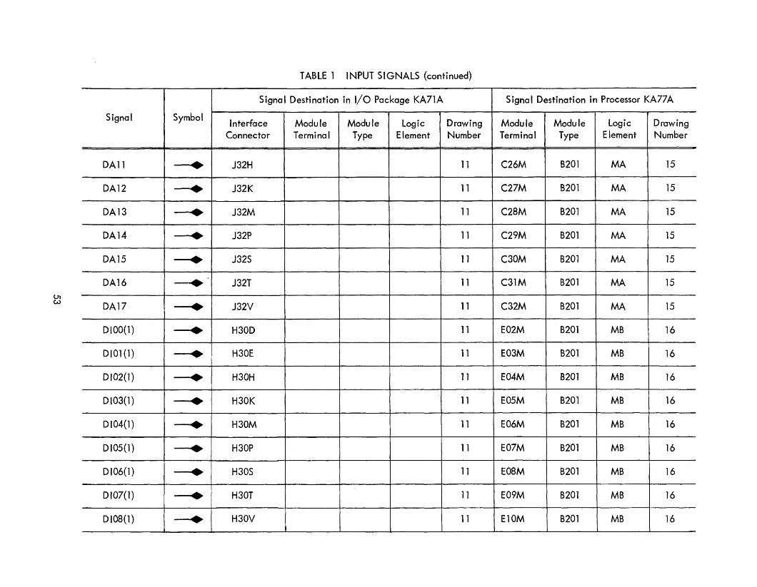
01 W
Signal
DAll
DA12
DA13
DA14
DA15
DA16
DA17
DIOO(1)
DlOl (1)
DI02(1)
DI03(1)
DI04(1)
DI05(1)
D 106(1)
0107(1)
0108(1)
Symbol
• --+
--+
--+
--+
--+
--+
--+
--+
--+
--+
--+
--+
• --+
--+
TABLE 1 INPUT SIGNALS (continued)
Signal Destination in I/o Package KA71A
Interface Module Module logic Drawing Connector Terminal Type Element Number
J32H 11
J32K 11
J32M 11
J32P 11
J32S 11
J32T 11
J32V 11
H30D 11
H30E 11
H30H 11
H30K 11
H30M 11
H30P 11
H30S 11
H30T 11
H30V 11
Signal Destination in Processor KA77A
Module Module Logic prawing Terminal Type Element Number
C26M B201 MA 15
C27M B201 MA 15
C28M B201 MA 15
C29M B201 MA 15
C30M B201 MA 15
C31M B201 MA 15
C32M B201 MA 15
E02M B201 MB 16
E03M B201 MB 16
E04M B201 MB 16
E05M B201 MB 16
E06M B201 MB 16
E07M B201 MB 16
E08M B201 MB 16
E09M B201 MB 16
E10M B201 MB 16

TABLE 1 INPUT SIGNALS (continued)
Signa I Destination in I/o Package KA71A Signal Destination in Processor KA77A
Signal Symbol Interface Module Module Logic Drawing Module Module Logic Drawing Connector Terminal Type Element Number Terminal Type Element Number
DI09(1) --+ J30D 11 EllM B201 MB 16
Dll0(1) --+ J30E 11 E12M B201 MB 16
DIll(1) --+ J30H 11 E13M B201 MB 16
DI12(1) --+ J30K 11 E14M B201 MB 16
DIl3(1) --+ J30M 11 E15M B201 MB 16
Di i4(1) --+ J30P 11 E16M B201 MB 16
~ DI15(1) --+ J30S 11 E17M B201 MB 16
DI16(l) --+ J30T 11 E18M B201 MB 16
D 117(1) --+ J30V 11 E19M B201 MB 16
ICOO(1) ---+ Jl0D 4 HJ2JL B210 AC 17 .
ICOl (l) --.-. J10E 4 HJ3JL B210 AC 17
iC02(1 ) ---+ jiOH 4 HJ4JL B210 AC 17
IC03(1) --.-. J10K 4 HJ5JL B210 AC 17
IC04(1) --+ J10M 4 HJ6JL B210 AC 17
IC05(1) --+ Jl0P 4 HJ7JL B210 AC 17
IC06(1) --+ Jl0S 4 HJ8JL B210 AC 17 -- - -- -- -_ .. _-_.-- -~-

0'1 0'1
Signal
IC07(1)
IC08(1)
IC09(1 )
IC1 0(1)
ICll (1)
IC12(1)
IC13(1)
IC14(1)
IC15(1)
IC16(1)
IC17(1)
lOT 0102(B)
lOT 0304(B)
MQl----. AC
lOT 7502
lOT 7404
Symbol
---+
--+
--+
--+
--+
--+
--+
--+
--+
--+
--+
--+
--+
--+
--+
--+
TABLE 1 INPUT SIGNALS (continued)
Signal Destination in I/o Package KA71A
Interface Module Module Logic Drawing Connector Terminal Type Element Number
JI0T 4
J10V 4
JllD 4
JllE 4
JllH 4
Jll K 4
JllM 4
JllP 4
J11S 4
JllT 4
J11V 4
E01E R141 IC 4
E01H R141 IC 4
E01K R141 IC 4
J23E E01M R141 IC 4
E01P R141 IC 4
Signal Destination in Processor KA77A
Module Module Logic Drawing Terminal Type Element Number
HJ9JL B210 AC 17
HJ10JL B210 AC 17
HJllJL B210 AC 17
HJ12JL B210 AC 17
HJ 13JL B210 AC 17
HJ14JL B210 AC 17
HJ15JL B210 AC 17
HJ16JL B210 AC 17
HJ 17 JL B210 AC 17
HJ18JL B210 AC 17
HJ19JL B210 AC 17

01 0-
Signal
lOT 7602
lOT 7304
Symbol
--+
--+
TABLE 1 INPUT SIGNALS {continued}
Signal Destination in I/o Package KA71A
Interface Module Module Logic Drawing Connector Terminal Type Element Number
E01S R14l IC 4
E01U R14l IC 4
Signal Destination in Processor KA77A
Module Module Logic Drawing Terminal Type Element Number
~

OJ 'J
Signal
ACBOO(1 )
ACB01 (1)
ACB02(1 )
ACB03(l )
ACB04(1 )
ACB05(l)
ACB06(l )
ACB07(l )
ACB08(1 )
ACB09(l )
ACB1O(l)
ACB 11 (1 )
ACB12(l)
ACB13{1 )
ACB14{l)
ACB15(l)
Symbol
--<>
--<>
--<>
--<>
--<>
--<>
--<>
--<>
--<>
--<>
--<>
--<>
--<>
-<>
-<>
-<>
TABLE 2 OUTPUT SIGNALS
Signal Origin in I/O Package KA71 A
Interface Module Module Logic Drawing Connector Terminal Type Element Number
H14D-H21 D W021 ID 11
H14E-H21 E W021 ID 11
H14H-H21 H W021 ID 11
H14K-H21 K W021 ID 11
H14M-H21M W021 ID 11
H14P-H21 P W021 ID 11
H14S-H21 S W021 ID 11
H14T -H21T W021 ID 11
H14V-H21V W021 ID 11
J14D-J21 D W021 ID 11
J14E-J21 E W021 ID 11
J14H -J21 H W021 ID 11
J14 K-J21 K W021 ID 11
J14M-J21M W021 ID 11
J14P-J21 P W021 i
I ID 11
J14S-J21 S W021 ID 11
Signal Origin in Processor KA77A
Module Module Logic Drawing Terminal Type Element Number
M03J R650 AC Bus Drivers 18
M03T R650 AC Bus Drivers 18
M04J R650 AC Bus Drivers 18
M04T R650 AC Bus Drivers 18
M05J R650 AC Bus Drivers 18
M05T R650 AC Bus Dr i vers 18
M06J R650 AC Bus Drivers 18
M06T R650 AC Bus Drivers 18
M07J R650 AC Bus Drivers 18
M07T R650 AC Bus Drivers 18
M08J R650 AC Bus Drivers 18
M08T R650 AC Bus Drivers 18
M09J R650 AC Bus Dri vers 18
M09T R650 AC Bus Drivers ! 18
M10J R650 I I
I AC Bus Drivers i 18
M10T R650 I
I AC Bus Drivers 18 l

U1 co
-,-
Signal
ACB 16(1) ------
ACB17(1)
IOTOO02
IOTOO04
IOT0102
IOT0104
IOT0202 --' ...
IOT0204
IOT0302
IOT0304
IOT0402
IOT0404
IOT0502
IOT0504
IOT0602
IOT0604
Symbol Interface Connector
--<> J14T-J13T
--<> J14V-J13V
--{>
--{>
--{>
---{>
---t>
---{>
---t>
---{>
---I>
--t>
---{>
---{>
---I>
----t>
TABLE 2 OUTPUT SIGNALS (continued)
Signal Origin in I/O Package KA71 A Signal Origin in Processor KA77A
Module Module Logic Drawing Module Module Logic Drawing Terminal Type Element Number Terminal Type Element Number
W021 ID 1 1 MllJ R650 AC Bus Drivers 18
W021 ID 11 MllT R650 AC Bus Drivers 18
D25F R603 DS 5
D25M R603 DS 5
D21T R603 DS 5
D21F R603 DS 5
D22M R603 DS 5
D22T R603 DS 5
D23F R603 DS 5
D23M R603 DS 5
D23T R603 DS 5
D24F R603 OS 5
C23F R603 OS 5
C23M R603 DS 5
C23T R603 OS 5
C24F R603 OS 5
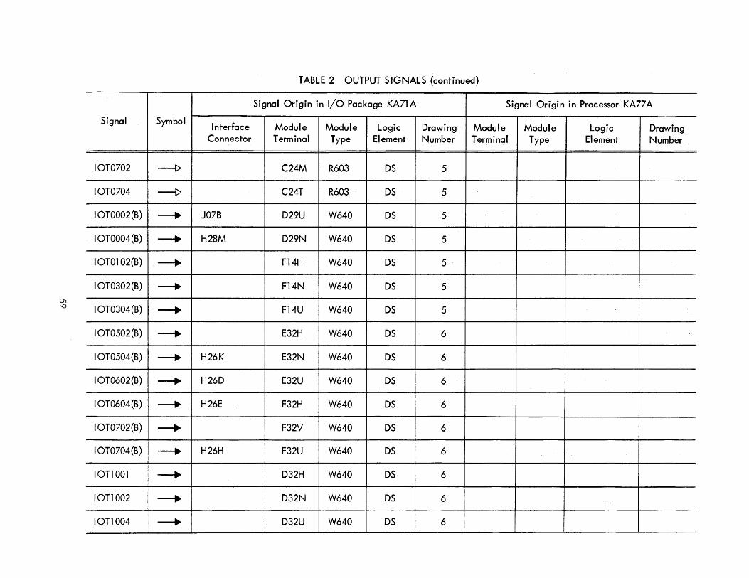
lJl -.0
Signal
IOT0702
IOT0704
IOTOO02{B)
IOTOO04{B)
IOT0102{B)
IOT0302{B)
IOT0304{B)
IOT0502{B)
IOT0504(B)
IOT0602(B)
IOT0604(B)
IOT0702(B)
IOT0704(B)
Ion 001
Ion 002
IOT1004
Symbol Interface
Connector
--t>
--1>
--+ J07B
--+ H28M
--+
--+
--+
--+
--+ H26K
--+ H260
--+ H26E
--+
--+ H26H
--+
--+
--+
TABLE 2 OUTPUT SIGNALS (continued)
Signal Origin in I/O Package KA71 A Signal Origin in Processor KA77A
Module Module Logic Drawing Module Module Logic Drawing Terminal Type Element Number Terminal Type Element Number
C24M R603 DS 5
C24T R603 DS 5
029U W640 OS 5
D29N W640 OS 5
F14H W640 DS 5
F14N W640 DS 5
F14U W640 OS 5
E32H W640 DS 6
E32N W640 DS 6
E32U W640 DS 6
F32H W640 DS 6
F32V W640 DS 6
F32U W640 DS 6
032H W640 DS 6
032N W640 OS 6
i 032U W640 DS 6 !

0-.. o
TABLE 2 OUTPUT SI GNALS (continued)
Signal Origin in I/O Package KA71 A Signal Origin in Processor KA77A
Signal
IOTll01
IOTl102
IOTll04
IOTl201
IOT1202
Symbol
~
--+
--. --+
--.
Interface Connector
J24D
J24E
J24H
Module Module I Logic Terminal Type Element
Drawing Module Module Number Terminal Type
F30H W640 DS 6
F30N W640 DS 6
E30H W640 DS 6
F30U W640 DS 6
E31 N W640 DS 6
_1~_Tl20~J~~ __ 1 E31U W640 DS 6
IOT1301 I --+ F31H W640 DS 6 .-- '." ..... -....... ' ...... -J .-.. -- ... _._ .. ········--t--·-·----···-,.-· .. ·-·.--·--+
IOTl302 I --+ H23E F31 N W640 DS 6 I
Logic Element
Drawing Number
I0T1304 I -'---l-I _H2_3K_---+-_----+_--+_-----t __ -+--_-+---_-+---__ -+-__ F31U W640 DS 6
IOT2101 --+ I
IOT2102 I --+ _.. ,--+1---
IOT2104 I --+ I --_ .. __ . __ -1-.. _-t-
IOT7002 I --+ I H24D
IOT7004 --+ H24E
IOT7102 --+ H24H
IOT7104 ~ H24K
E27H W640 DS 6
E27N W640 DS 6
E27U W640 DS 6
F27H W640 DS 6
F27N W640 DS 6
F27U W640 DS 6
E28H W640 DS 6

TABLE 2 OUTPUT SIGNALS (continued)
Signal Origin in I/O Package KA71 A Signal Origin in Processor KA77 A
Signal Symbol Interface Module Module Logic Drawing Module Module Logic Drawing Connector Terminal Type Element Number Terminal Type Element Number
IOT7202 ---+ H24M E28N W640 DS 6
IOT7204 ---+ H24P E28U W640 DS 6
IOT7301 ---+ F28H W640 DS 6
IOT7302 ~ H24S F28N W640 DS 6
IOT7304 --+ F28U W640 DS 6
IOT7401 -+ H24T E29H W640 DS 6
().. ....... IOT7402 ---+ H24V E29N W640 DS 6
IOT7404 -+ H25D E29U W640 DS 6
IOT7501 -+ J23D F29H W640 DS 6
IOT7502 ---+ J23E F29N W640 DS 6
IOT7504 ---+ J23H F29U W640 DS 6
IOT7601 ---+ E30H W640 DS 6
IOT7602 -+ E30N W640 DS 6
IOT7604 ---+ J23K E30U W640 DS 6
MBB04(O) i --+ J03D 11 D07D B684 MB Bus Drivers 18
MBB05(O) --+ J03E 11 D07N B684 MB Bus Drivers 18

0-I'.)
Signal
MBB06(B)
MBB07(0)
MBB08(0)
MBB09(0)
MBB10(0)
MBBll (0)
MBB12(0)
MBBOO(1 )
MBB01 (1)
MBB02(1 )
MBB03(1 )
MBB04(1 )
MBB05(1 )
MBB06(1 )
MBB07(1 )
MBB08(1 )
Symbol
--+
--+
--+
--+
--+
--+
--+
--+
--+
--+
• • •
--+ I
--+
--+
Interface Connector
J03H
J03K
J03M
J03P
J03S
J03T
J03V
H02D
H02E
H02H
H02K
H02M
H02P
H02S
H02T
H02V
TABLE 2 OUTPUT SIGNALS (continued)
Signal Origin in I/O Package KA71 A Signal Origin in Processor KA77 A
Module Module Logic Drawing Module Module Logic Drawing Terminal Type Element Number Terminal Type Element Number
11 D09D B684 MB Bus Drivers 18
11 D09N B684 MB Bus Drivers 18
11 D11 D B684 MB Bus Drivers 18
11 D11 N B684 MB Bus Drivers 18
11 D13D B684 MB Bus Drivers 18
11 D13N B684 MB Bus Drivers 18
11 D15D B684 MB Bus Drivers 18
W21 ID 11 D22D B684 MB Bus Drivers 18
W21 ID 11 D22N B684 MB Bus Drivers 18
W21 ID 11 D23D B684 MB Bus Drivers 18
W21 ID 11 D23N B684 MB Bus Drivers 18
W21 ID 11 D24D B684 MB Bus Drivers 18
W21 ID 11 D24N B684 MB Bus Drivers 18
W21 ID 11 D25D B684 MB Bus Drivers 18
W21 ID 11 D25N B684 MB Bus Drivers 18
W21 ID 11 D26D B684 MB Bus Drivers 18

0-W
Signal
MBB09{1 )
MBB1 0(1)
MBB11 (1)
MBB12(1 )
MBB13(l )
MBB14(1 )
MBB15(1 )
MBB16(1 )
MBB17(1 )
Symbol
• ~
~
• • • • • ~
Interface Connector
J02D
J02E
J02H
J02K
J02M
J02P
J02S
J02T
J02V
TABLE 2 OUTPUT SIGNALS (continued)
Signal Origin in I/O Package KA71 A Signal Origin in Processor KA77 A
Module Module Logic Drawing Module Module Logic Drawing Terminal Type Element Number Terminal Type Element Number
W21 ID 11 D26N B684 MB Bus Drivers 18
W21 ID 11 D27D B684 MB Bus Drivers 18
W21 ID 11 D27N B684 MB Bus Drivers 18
W21 10 11 D28D B684 MB Bus Drivers 18
W21 10 11 D28N B684 MB Bus Drivers 18
W21 ID 11 D29D B684 MB Bus Drivers 18
W21 ID 11 D29N B684 MB Bus Drivers ' 18
W21 10 11 D30D B684 MB Bus Drivers 18
W21 ID 11 D30N B684 MB Bus Drivers 18

TABLE 3 PREWIRED INTERFACE CONNECTIONS
Signal Terminal Signal Terminal
57 A Automatic Magnetic Tape Control
ACB 00(1) H16D ACB 09(1) J16D
ACB 01(1) H16E ACB 10(1) J16E
ACB 02(1) H16H ACB 11 (1) J16H
ACB 03(1) H16K ACB 12(1) J16K
ACB 04(1) H16M ACB 13(1) J16M
ACB 05(1) H16P ACB 14(1) J16P
ACB 06(1) H16S ACB15(1) J16S
ACB 07(1) H16T ACB 16(1) J16T
ACB 08(1) H16V ACB 17(1) J16V
lOT 7002 H24D lOT 7404 H25D
lOT 7004 H24E PWR CLR NEG H25E
lOT 7102 H24H BGN (B) H25H
lOT 7104 H24K MBB 12(1) H25K
lOT 7202 H24M MBB 12(0) H25M
lOT 7204 H24P H25P
lOT 7302 H24S H25S
lOT 7401 H24T H25T
lOT 7402 H24V H25V
ERF-ERF ENB J25D H07D
WCO-WCO ENG J25E H07E
TCR J25H H07H
T READY J25K CA 03(1) H07K
DATA ACC J25M CA 04(1) H07M
ADDRESS ACC J25P CA 05(1) H07P
DATA IN J25S CA 06(1) H07S
DATA RQ J25T CA 07(1) H07T
J25V CA 08(1) H07V
64

TABLE 3 PREWIRED INTERFACE CONNECTIONS (continued)
Signal Terminal Signal Terminal
57 A Automatic Magnetic Tape Control (continued)
CA 09(1) H08D DR LATE H10D
CA 10(1) H08E PARITY ERR H10E
CA 11 (l) H08H READ COMP ERR H10H
CA 12(1) H08K EOF H10K
CA 13(1) H08M WRITE LOCK H10M
CA 14(1) H08P LOAD POINT H10P
CA 15(1) H08S END POINT H10S
CA 16(1) H08T TRD/WR LR H10T
CA 17(1) H08V A/B FR H10V
REWIND HllD
MISS CHAR HllE
57A JOB DONE H11 H
(F04V) Hl1 K
(F05V) H11M
(F06V) Hl1P
(F07V) H11 S
(F08V) Hll T
(F09V) HllV
138 Analog-to-Digital Converter
H10D Hl1 D
H10E HllE
H10H Hl1 H
H10K (F04V) Hl1 K
H10M (F05V) H11 M
H10P (F06V) Hl1P
H10S (F07V) Hl1S
H10T (F08V) HllT
H10V (F09V) HllV
65

TABLE 3 PREWIRED INTERFACE CONNECTIONS (continued)
Signal Terminal Signal Terminal
138 Analog-to-Digital Converter (continued)
H23D
H23E
H23H
(F04V) H23K
(F05V) H23M
(F06V) H23P
(F07V) HllS
(F08V) HllT
(F09V) Hl1V
139 Multiplexer
ACB 09(1) J20D lOT 11 01 J24D
ACB 10(1) J20E lOT 1102 J24E
ACB 11 (1) J20H lOT 1201 J24H
ACB 12(1) J20K CA 12(1) J24K
ACB 13(1) J20M CA 13(1) J24M
ACB 14(1) J20P CA 14(1) J24P
ACB 15(1) J20S CA 15(1) J24S
ACB 16(1) J20T CA 16(1) J24T
ACB17(1) J20V CA 17(1) J24V
140 Relay Buffer
ACB 00(1) H19D ACB 09(1) J19D
ACB01(l) H19E ACB 10(1) J19E
ACB 02(1) H19H ACBll(l) J19H
ACB 03(1) H19K ACB12(1) J19K·
ACB 04(1) H19M ACB 13(1) J19M
ACB 05(1) H19P ACB 14(1) J19P
ACB 06(1) H19S ACB15(1) J19S
ACB 07(1) H19T ACB 16(1) J19T
ACB 08(1) H19V ACB 17(1) J19V
66
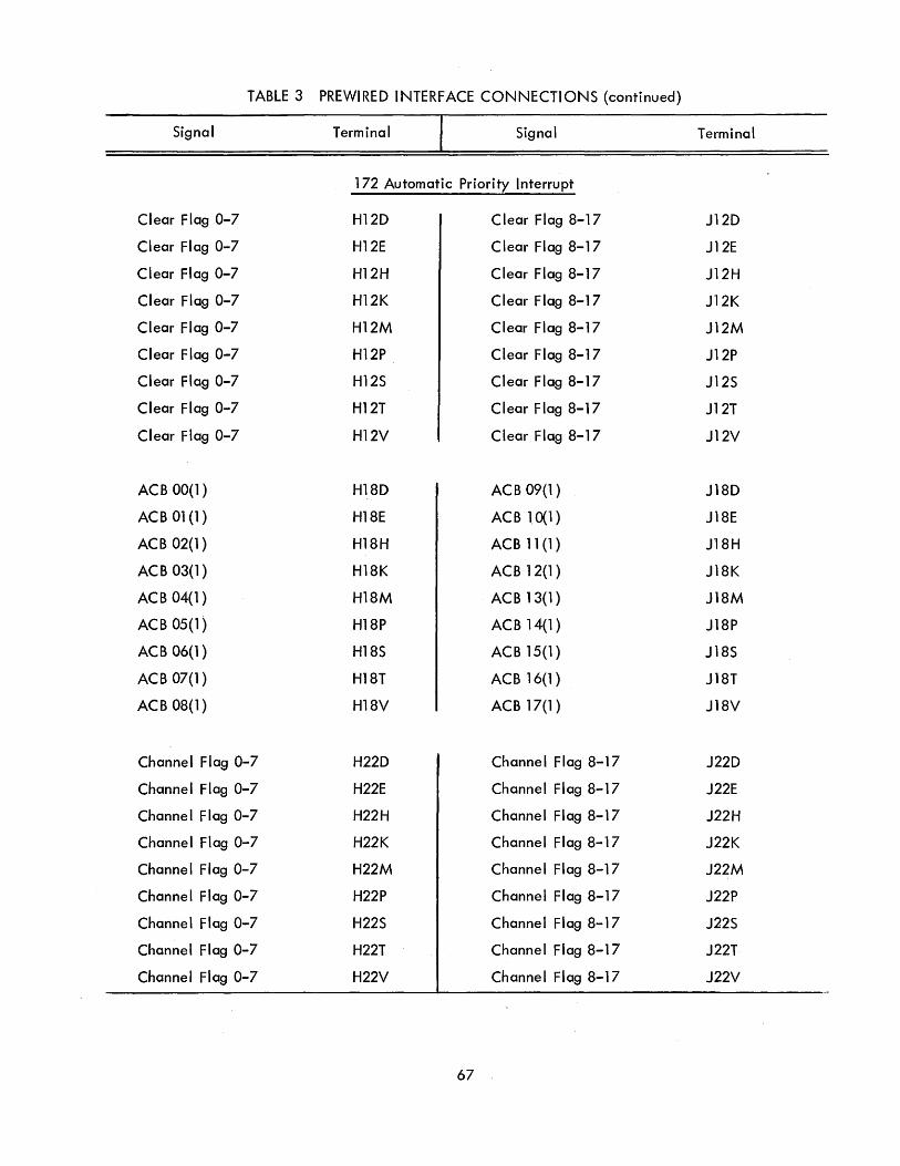
TABLE 3 PREWIRED INTERFACE CONNECTIONS (continued)
Signal Terminal Signal Terminal
172 Automatic Priority Interrupt
Clear Flag 0-7 H12D Clear Flag 8-17 J12D
Clear Flag 0-7 H12E Clear Flag 8-17 J12E
Clear Flag 0-7 H12H Clear Flag 8-17 J12H
Clear Flag 0-7 H12K Clear Flag 8-17 J12K
Clear Flag 0-7 H12M Clear Flag 8-17 J12M
Clear Flag 0-7 H12P Clear Flag 8-17 J12P
Clear Flag 0-7 H12S Clear Flag 8-17 J12S
Clear Flag 0-7 H12T Clear Flag 8-17 J12T
Clear Flag 0-7 H12V Clear Flag 8-17 J12V
ACB 00(1) H18D ACB 09(1) J18D
ACB 01 (l) H18E ACB10(1) J18E
ACB 02(1) H18H ACB 11(1) J18H
ACB 03(1) H18K ACB 12(1) J18K
ACB 04(1) H18M ACB 13(1) J18M
ACB 05(1) H18P ACB 14(1) J18P
ACB 06(1) H18S ACB 15(1) J18S
ACB 07(1) H18T ACB 16(1) J18T
ACB 08(1) H18V ACB 17(1) J18V
Channel Flag 0-7 H22D Channel Flag 8-17 J22D
Channel Flag 0-7 H22E Channel Flag 8-17 J22E
Channel Flag 0-7 H22H Channel Flag 8-17 J22H
Channel Flag 0-7 H22K Channel Flag 8-17 J22K
Channel Flag 0-7 H22M Channel Flag 8-17 J22M
Channel Flag 0-7 H22P Channel Flag 8-17 J22P
Channel Flag 0-7 H22S Channel Flag 8-17 J22S
Channel Flag 0-7 H22T Channel Flag 8-17 J22T
Channel Flag 0-7 H22V Channel Flag 8-17 J22V
67
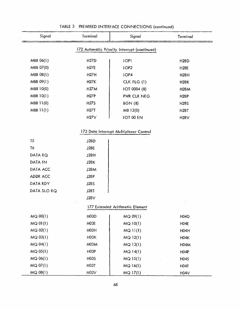
TABLE 3 PREWIRED INTERFACE CONNECTIONS (continued)
Signal Terminal Signal Terminal
172 Automatic Priority Interrupt (continued)
MBB 06(1) H27D IOP1 H28D
MBB 07(0) H27E IOP2 H28E
MBB 08(1) H27H IOP4 H28H
MBB 09(1) H27K ClK FlG (1) H28K
MBB 10(0) H27M lOT 0004 (B) H28M
MBB 10(1) H27P PWR CLR NEG H28P
MBB 11 (0) H27S BGN (B) H28S
MBB 11 (1) H27T MB 12(0) H28T
H27V lOT 00 EN H28V
173 Data Interrupt Multiplexer Control
T5 J28D
T6 J28E
DATA RQ J28H
DATA IN J28K
DATA ACC J28M
ADDR ACC J28P
DATA RDY J28S
DATA SLO RQ J28T
J28V
177 Extended Arithmetic Element
MQ 00(1) H03D MQ 09(1) H04D
MQ 01 (1) H03E MQ 10(1) H04E
MQ 02(1) H03H MQ 11 (1) H04H
MQ 03(1) H03K MQ 12(1) H04K
MQ 04(1) H03M MQ 13(1) H04M
MQ 05(1) H03P MQ 14(1) H04P
MQ 06(1) H03S MQ 15(1) H04S
MQ 07(1) H03T MQ 16(1} H04T
MQ 08(1) H03V MQ 17(1} H04V
68

TABLE 3 PREWIRED INTERFACE CONNECTIONS (continued)
Signal Terminal Signal Terminal
177 Extended Arithmetic Element (continued)
ACB 00(1) H14D ACB 09(1) J14D
ACB01(1) H14E ACB 10(1) J14E
ACB 02(1) H14H ACB 11 (1) J14H
ACB 03 (1) H14K ACB 12(1) J14K
ACB 04(1) H14M ACB13(1) J14M
ACB 05(1) H14P ACB 14(1) J14P
ACB 06(1) H14S ACB 15(1) J14S
ACB 07(1) H14T ACB 16(1) J14T
ACB 08(1) H14V ACB 17(1) J14V
SC1-AC Jll D
MQ1-AC JllE
Jll H
SC 12(1) J11 K
SC 13(1) Jl1M
SC 14(1) Jll P
SC 15(1) Jll S
SC 16(1) Jll T
SC 17(1) JllV
340 Precision Incremental Display
H10D Hll D
H10E HllE
H10H H11 H
H10K (F04V) Hll K
H10M (F05V) HllM
H10P (F06V) HllP
H10S (F07V) Hll S
H10T (F08V) HllT
H10V (F09V) HllV
69

TABLE 3 PREWIRED INTERFACE CONNECTIONS (contiinued)
Signal Terminal Signal Terminal
340 Precision Incremental Display (continued)
ACB 00(1) H17D ACB 09(1) J17D
ACB 01 (1) H17E ACB 10(1) J17E
ACB 02(1) H17H ACB 11 (1) J17H
ACB 03(1) H17K ACB 12(1) J17K
ACB 04(1) H17M ACB 13(1) J17M
ACB 05(1) H17P ACB 14(1) J17P
ACB 06(1) H17S ACB 15(1) J17S
ACB 07(1) H17T ACB 16(1) J17T
ACB 08(1) H17V ACB 17(1) J17V
lOT 0602 (B) H26D STOP FIG J26D
lOT 0604 (B) H26E 340 LP FLG J26E
lOT 0704 (B) H26H DATA RQ J26H
lOT 0504 (B) H26K DATA IN J26K
H26M ADDR ACC J26M
H26P DATA ACC J26P
H26S BGN J26S
H26T V EDGE FLG J26T
H26V HEDGE FLG J26V
550 DECtape Control
DTI 00(1) H05D DTI 09(1) H06D
DTI 01 (1 ) H05E DTI 10(1) H06E
DTI 02(1) H05H DTI 11 (1 ) H06H
DTI 03(1) H05K DTI 12(1) H06K
DTI 04(1) H05M DTI 13(1) H06M
DTI 05(1) H05P DT114(l) H06P
DTI 06(1) H05S Drl 15(1) H06S
DTI 07(1) H05T DTI 16(1) H06T
DTI 08(1) H05V DTI 17(1) H06V
70

TABLE 3 PREWIRED INTERFACE CONNECTIONS (continued)
Signal Terminal Signal Terminal
550 DEC tape Control (continued)
ACB 00(1) H15D ACB 09(1) J15D
ACB 01 (1) H15E ACB10(1) J15E
ACB 02(1) H15H ACB 11 (1) J15H
ACB 03(1) H15K ACB 12(1) J15K
ACB 04(1) H15M ACB 13(1) J15M
ACB 05(1) H15P ACB 14(1) J15P
ADB 06(1) H15S ACB15(1) J15S
ACB 07(1) H15T ACB 16(1) J15T
ACB 08(1) H15V ACB 17(1) J15V
DATA FLG H09D lOT 7501 J23D
BLK FLG H09E lOT 7502 H23E
ERR FLG H09H lOT 7504 H23H
OFF END H09K lOT 7604 H23K
MISS IND H09M RUN (1) B H23M
REV STATUS H09P MBB 12(1) H23P
GO H09S 550 lOT 7501 H23S
MK TRK ERR H09T 550 lOT 7541 H23T
UNABLE H09V PWR CLR NEG H23V
Unspecified Data Break Device
MBB 00(1) H02D MBB 09(1) J02D
MBB 01 (l) H02E MBB 10(1) J02E
MBB 02(1) H02H MBB 11(1) J02H
MBB 03(1) H02K MBB 12(1) J02K
MBB 04(1) H02M MBB 13(1) J02M
MBB 05(1) H02P MBB 14(1) J02P
MBB 06(1) H02S MBB 15(1) J02S
MBB 07(1) H02T MBB 16(1) J02T
MBB 08(1) H02V MBB 17(1) J02V
71

TABLE 3 PREWIREO INTERFACE CONNECTIONS (continued)
Signal Terminal Signal Terminal
Unspecified Oota Break Oevice (continued)
0100 H300 0109 J300
0101 H30E 01 10 J30E
0102 H30H 01 11 J30H
0103 H30K 01 12 J30K
0104 H30M 01 13 J30M
0105 H30P 01 14 J30P
0106 H30S 01 15 J30S
0107 H30T DI 16 J30T
0108 H30V 0117 J30V
H320 OA 09 J320
H32E OA10 J32E
H32H OA 11 J32H
OA 03 H32K OA 12 J32K
OA 04 H32M OA 13 J32M
OA 05 H32P OA14 J32P
OA 06 H32S OA15 J32S
OA 07 H32T OA16 J32T
OA 08 H32V OA17 J32V
T5 J28D
T6 J28E
OATA RQ J28H
OATA IN J28K
OATA ACC J28M
AOOR ACC J28P
OATA ROY J28S
DATA SLO RQ J28T
J28V
72

The R650 Bus Driver has two types of outputs: fast and slow (or ramp). Using fast output, the bus driver
operates as a fast amplifier. When ramp output is used, an integrating capacitor is inserted between the
input of the bus driver and the output stage, causing the output lines to move from ground to - 3v (or
reverse) in approximately 800 nsec. This connection, desirable to reduce crosstalk between lines, is
used on the ACB (buffered accumu lator) lines.
The W640 Pulse Amplifier modules should be carefully terminated. If sufficient noise is generated at the
output of these modu les, regeneration may resu It. For this reason, it is recommended that output lines of
W640 Pulse Amplifier modules be well shielded. The outputs of W640 modules may be either 400 nsec or
1 ~sec in width. All connection.s on the standard PDP-7 use the 400 nsec pulse width.
All input signals to the PDP-7 are received by diode gates or inverters. Diode gate inputs draw 1 rna of
current from the driving circuit, shared among all inputs at ground potential. Inverter inputs draw 2 rna
when the signal is at - 3v and provide no load when the signal is at ground potential.
Timing is, in general, determined by the machine itself. However, the following timing considerations
apply to the modules. The Rl11 Diode Gate sets up in approximately 50 nsec in either direction under
normal load conditions.
The DCD gates set up in 400 nsec, from the end of the preceding 100-nsec pulse; and the pulse input must
return to - 3v for 400 nsec before the next pulse is applied. Series R pulses are 100 nsec in width,
measured from the 90% point of the leading edge to the 10% point of the trailing edge. Fall time is not
critical on these pulses, provided that the pulse has returned to - 3v in time to come up for the next cycle.
All output signals from the PDP-7, routed through the interface, have been provided with adequate buf
fering to meet the input requirements of normal I/O equipment. Whenever it becomes necessary for the
user to draw out other signals (besides those connected in the standard interface), care must be taken that
the input loads presented to the sources of these signals do not exceed their driving obi lity. When it is
evident that the source would be overloaded, a suitable driver must be provided between the signal source
and the I/O device employing the signal.
Device Selector
The DS generates lOT pulses that control I/O equipment and effect information transfers between the
computer and peripheral devices. The DS contains a section for standard devices (program interrupt con
trol, real time clock interrupt control, tape reader, tape punch, Teletype units, and display equipment;
73

or device select codes 00 through 07), and a section for optional equipment (used to expand the DS for
all other select codes). Each channel of the ()ptional DS consists of a Type W103 Device Selector module
and a W640 Pulse Amplifier module.
Complementary output signals from bits 6-11 of the lOT instruction in the MB ~::Ire di stributed to all
channels of the optional DS. These six bits serve as a device select code. The 1 or 0 signal from each
MB bit is wired or disconnected in each WI03 module to enable a gate only wlhen a pre-established select
code occurs in the lOT instruction. When enabled by the correct select code, the WI03 module repro
duces any lOP pulses as complementary lOT command pulses. Positive lOT pulses are buffered by a cir
cuit of aW640 module before being transmitted over long cables to peripheral devices. These pulses are
used in I/O devices for ,functions such as clearing flags, gating data, setting operation modes, etc. The
last digit of any lOT pulse designation corresponds to the number of the lOP pulse which causes generation
of that lOT pulse (e.g., combination of a device code XX with an IOP4 pulse produces an lOT XX04
pulse). lOT select code assignments are given in Table 4.
Pu Ise outputs of the WI03 Device Selector modu Ie are 100-nsec or 400-nsec co,lIector outputs and can
drive any standard R-series FLIP CHIP module located in the proximity of the I/O package. However,
most options are located at some distance and require signal transmission over relatively long cables.
The W640 Pulse Amplifier modules are capable of driving cables and are wired into appropriate locations
to transmit lOT pulses to external devices. The W640 produces 400-nsec pulses (or 1-jJsec pulses when
appropriate terminals are connected together).
Information Collector
The IC reads data or status information into the AC from various devices. SeveniC channels or levels are
available in the basic machines. Each of thesE~ channels is wired to a signal cClble connector correspond
ing to an upper half (bits 0-8) and a lower half (bits 9-17) of the AC for optional equipment, or is wired
directly to controls for the standard PDP-7 I/O equipment. On the basic machine, the paper-tape reader
occupies one complete channel, the Teletype occupies the lower half of a channel, and the status register
occupies (nominally) one channel. If no card reader, card punch, or line printer is connected to the
system, the lower half of the status register channel may be used for other purp1oses. Thus, in the basic
machine, the equivalent of five free channels is available for additional IC inputs. Channel availability
of the IC is specified as follows:
74

TABLE 4 lOT CODE ASSIGNMENTS
00 1 RT Clock 10 Symbol 20 Memory 30 40 50 60 Serial 70 Auto Magnetic 2 Prog. Interrupt Generator Increment Drum Tape Control 4 RT Clock Type 33 Type 197 Type 24 Type 57A
01 Standard 11 Analog-to- 21 Relay Buffer 31 41 51 61 Serial 71 Tape Control Perforated Digital or Type 140 Drum Type 57A Tape Reader Digital-to- Type 24 and Control Analog
Converters
02 Standard 12 A-D-A 22 Inter-Processor 32 42 52 62 Serial 72 Tape Control Perforated Buffer Drum Type 57A Tape Punch Type 195 Type 24
03 1 Keyboard 13 A-D-A 23 Inter-Processor 33 1 33 KSR Skip 43 53 63 73 Tape Control
2 Keyboard Stimulus Buffer 2 Clear All Type 57A
4 laRS Flag Type 195 Flags
~ 4 Open
04 Teleprinter 14 24 Incremental 34 44 54 64 74 Tape Control
Plotter Type 57A Control Type 350
05 Displays 15 25 Plotter 35 45 55 Automatic 65 Automatic 75 DECtape
Types 34F, Priority Line Printer Control
300, or 340 Interrupt Type 647 Type 550 Type 172
06 Displays 16 26 Plotter 36 46 56 API 66 Automatic 76DECtape Type 172 Line Printer Control
Type 647 Type 550
I
07 Display 17 Boundary 27 Memory 37 47 57 67 Card Reader 77 Memory
and Register Parity Type CR 01 B Extension
light Pen Type KA70A Type 176 or Type CR 02A Type 148B
Level
2
3-5
6
7
Use
All 18 connections employed for RB of the tape reader.
First 9 connections employed for status signals of 10RS instruction (lOT 0314), and last 6 connections are assigned to the step counter (SC) of the Type: 177 EAE option, when present.
All 18 connections open and assignable.
First 10 connections are open and last 8 connections are assigned to Teletype unit.
First 12 connections open and assignable.
Each level or channel of the IC consists of one 2-input negative AND gate for each of the 18 possible
bits of an input word. The two inputs are usually supplied by a data signal and an lOT pulse which is
common to each bit of the input word. Outputs from the seven channels for eClch bit are NOR combined
to set the appropriate accumulator flip-flop. One bit for each of the seven channels is provided by a
Type R141 Diode Gate module; the entire IC is constructed of 18 of these modules.
When designing a PDP-7 system, it is necessary to consider the number of IC channels required by peri
pheral equipment. If more than seven channels are required, the IC must be expanded to accommodate
the additional information. Expansion requires a Type 175 Information Collect-or Expander consisting of
18 Type R141 Diode Gate modules, 6 Type W640 Pulse Amplifier modules, and the appropriate mounting
panel and hardware. The Type 175 option connects into the standard IC throus,h two signal cable con
nectors reserved for this purpose, and adds seven additional information channEds. Figure 28 represents the
channel assignments for the standard IC.
Information Distributor
Data in the AC is available at the ID of the computer interface as static levels. lOT pulses from the DS
can strobe these static levels into an I/O device register. The static level of E~ach ACB output signal is
- 3v when the bit is a binary 0 or is at ground potential when the bit is a binary 1 •
The binary 1 output of each AC flip-flop is power amplified by a Type R650 Bus Driver module in the
processor and is applied to the ID for distribution to output devices. These modules have terminals Hand
S connected to ground so that the output signals have a rise time of approximatlsly 800 nsec. (Without
these terminals grounded the rise time is about 50 nsec.) Each R650 output del'livers about 20 ma to ground 0
The ID provides a series of nine output channels for connection to external deviices for the buffered AC
signals in locations 13-21 of rows Hand J of the I/O package. The prewired connections of the ID to the
interface cable receptacles are listed in Table 3.
76
'J 'J
CHANNEL I CHANNEL 2 CHANNEL 3 CHANNEL 4 CHANNEL 5 CHANNEL 6 CHANNEL 7
,- A \( A H A \f A \( A \( A " A'--___ ---.,
* * * JI\ H03 H04 H05 H06: H07 Hoe: HOg * HIO HII I I ~ ~ I I
I I
MAGNETIC MAGNETIC I MAGNETIC TAPE I TAPE I TAPE
CONTROL I CONTROL I CONTROL 57A I 57A , 57A
CURRENT STATUS STATUS ADDITIONAL ADDRESS I I STATUS I
OR OR , OR
OR EXTENDED I ARITHMETIC DEC TAPE PRECISION DECTAPE STANDARD PRECISION PRECISION
STANDARD ELEMENT CONTROL INCREMENTAL CONTROL TELETYPE INCREMENTAL 'INCREMENTAL TAPE STATUS 177 550 DISPLAY 550 KEYBOARD
DISPLAY I DISPLAY READER EXTENDED MULTIPLIER DATA INPUT 3.40 STATUS BUFFER 340 I 340
I ARITHMETIC QUOTIENT DTIO-17 DISPLAY X REGISTER I Y REGISTER I ELEMENT REGISTER ADDRESS
I , 177 COUNTER STEP OR , OR
I COUNTER OR I I SC12-17
ANALOG-TO-'ANALOG-TO-I , ANALOG-TO- DIGITAL I DIGITAL DIGITAL CONVERTER I CONVERTER
I CONVERTER 138 I 138 J 139 ADBO-8 I ADB9-17 I I I
* DATA LINES PREWIRED; NO CABLE CONNECTORS NEEDED
Figure 28 Information Collector Channel Assignments
I
I

Power Clear Output Signals
The PWR CLR POS and PWR CLR NEG pulses generate in the I/O package during the first 5-sec interval
following setting of the POWER switch to the on position. These pulses initialize and clear processor
registers and controls during the power turnon period, and are available to perform similar functions in
external equipment. The PWR CLR POS signal is a 375-kc, 10CHlsec positive pulse generated in the
Type R401 Clock module at location C15. The PWR CLR NEG signal is a 400·-nsec negative. pulse pro
duced in a pulse amplifier of the Type W640 module at location C13 that is triiggered by the PWR CLR POS
pu Ises.
Begin Buffered Output Signal
The BGN (B) signal is supplied to external equipment through a connection in the I/O package interface.
This signal is a 400-nsec, - 3v pulse generated by a W640 Pulse Amplifier at location C13 of the I/O
package during timing pulse SP1-CONTINUE NOT. In I/O equipment, the siignal clears registers and
resets control fl ip-flops to initial conditions when the START key on the PDP-7 operator console is operated.
Run Output Signal
The 1 output of the RUN flip-flop is supplied to external equipment through the interface circuits. This
RUN (1) signal is at - 3v when the computer is performing instructions and is at ground potential when
the program is halted. Magnetic tape and DECtape equipment use this signal to stop transport motion
when the PDP-7 halts, preventing the tape from running off the end of the reel.
Slow Cycle Request Input Signal
The device selector supplies the SLOW CYCLE REQUEST ground level signal tel request that all lOT in
structions which address a specific device be executed in a computer slow cycle. This signal is added
at the time a slow I/O device is added to the computer system. lOT instructiolns for the device are de
coded in a Type W103 Device Selector module. The ground level output at terminal BD when the device
is se lected requests the slow cyc Ie by connection to the input of a Type B171 Diode Gate modu Ie. Thi s
latter module is used as a ground level NOR gate for all such request signals, cmd a negative output on
terminal D of this module is applied to the processor timing circuits. The Type B171 module which re
ceives the SLOW CYCLE REQUEST signals from various devices is located at E14 of the I/O package.
Program Interrupt Request Input Signal
The flag of an external device can request a program interrupt. When the device requires servicing, the
condition of the flag, connected to the Type B124 Inverter module in location D27 of the I/O package,
78

can request a program break. (The flag of the external device shou Id also be connected to the I/O skip
facility so that the interrupt program can sense the lOT 01 pulse to determine the device requesting the
program break.) The PROGRAM INTERRUPT signal level is the NOR of requests from up to nine devices
that require programmed attention. The program interrupt faci I ity can be expanded to accommodate re
quests from nine additional devices by inserting another Type B124 module in location 028 of the I/O
package. When the program break is entered, a subroutine is initiated to determine which device, of
many, is to be serviced,and then to perform the appropriate service operation (usually by supplying or
receiving data under program control).
Data Break Request Input Signal
A high-speed I/O device may originate a data break req,uest by placing a - 3v DATA RQ level on the
request line connecting' the device to 'the computer. In the interrupt control, the DATA RQ level is
synchronized with delayed timing pu'lse T5 (T5-DLY) of the current computer cy~le, and sets the DATA
SYNC flip-flop to 1. This causes a BK RQ level to be transmitted to the major state generator. Com
pletion of the current instruction permits the major state generator to enter a break state, producing a (B)
level. This (B) level corribin'es with the DATA SYNC level to produce a negative DATA~B level.
An external device connected to the data break facility of the computer supplies a DATA RQ level, a
15-bit core memory address for the transfer, a signal indicating the direction of the transfer as into or
out of the computer core memory, and input or output connections to the MB for 18 data bits. The DATA
RQ level is sent to the computer at the time the data is ready fora' transfer into the PDP-7 or when the
data register in the external device is ready to receiv~ information from the PDP-7. This request level
must be - 3v for assertion, meaning a request for a data break, and drives a transistor base requiring 2 ma
of input current.
Transfer Direction Input Signal
This signal, specifying the direction of data transfer for a data break, is received by the computer from
the requesting device. Transfer direction is referenced to the computer core memory, not to the device.
This signal is a - 3v level when the transfer direction is in, or is ground for an out transfer. A 3-input
NAND diode gate for negative levels receives this signal at terminal N18F. The gate also receives the
internally generated DATA·B level and T3 pulse to cause generation of the DATA ACC pulse which strobes
the DI lines into the MB.
79

Data Address Input Signa I
During an ADDR ACC pulse of a break cycle, the data address given by an I/o device is transferred to
the MA by connections made at the DA level input of a NOR gate in each module of the MA.
Address Accepted Output Signal
At time T1 of the break cycle, the DATAeB level NAND combines with timinH pulse T1 to produce an
ADDR ACC pulse (called DATA ADDR ---.. MA pulse in early systems). This pulse transfers the memory
address in the address register of the I/O device into the processor MA. This pulse also acknowledges to
the external device that its address has been accepted.
Data Information Input Signals
The 18 DI lines establish the data to be transferred into the MB from an extern~:ll device during a data
break in which the direction of transfer is into the POP-7. The 01 signal levells; presented to 2-input
negative NAND diode gates at the binary 1 input of the MB, are transferred into the MB by the DATA
ACC pulse. This information in the MB is then written into core memory during a normal write operation.
The 01 signals are - 3v to designate a binary 1 or ground potential to specify C~ binary 0, and should be
avai lable at the time the break request is made •
. Data Accepted Output Signal
During time T3 of a data break cycle, when the external device requests a transfer into the POP-7, the
DATAeB level causes a negative DATA ACC pulse (called DATA INFO --+ MB in early systems) to be
generated. This pulse strobes the data input gates of the MB to transfer a data word from an external de
vice into the MB. This pulse is also an output for device synchronization. Sturting at time T5, infor
mation in the MB is written into core memory by the normal write operation.
Data Ready Output Signal
During T3 of a data break cycle in which the transfer direction is out, the DATA·B level causes a nega
tive DATA RDY (in early systems called MB INFO ---+- OUT) pulse to be generated. This pulse may strobe
MBB information into the external device buffer; for this purpose the signal may be delayed within the de
vice to strobe the data into the buffer after an appropriate setup time. Note that the transfer must occur
prior to T2 of the next computer cycle.
80

Data Information Output Signals
Data break transfer from core memory to an I/O device is made through the MB, whose output is buffered
for this purpose by 18 Type B684 Bus Drivers. Each bus driver is capable of driving a 4O-ma load. The
MBB output terminals are in the I/O package.
81


CHAPTER 6
INSTALLATION PLANNING
PHYSICAL CONFIGURATION
The basic PDP-7 is housed in a three-bay cabinet and consists essentially of mounting panels of FLIP CHIP
modu les. Figure 29 shows the physical location of the memory , processor, I/O package, operator con
sole, tape reader, and tape punch within the basic system. Space is available for optional equipment
below the table in the center bay and above the I/O package in the right bay. For example, a three
bay PDP-7 with 8192 words of core memory could also include an Automatic Priority Interrupt Type 172B
and have space foranalog-to-digital or CRT display options. Larger systems are constructed by adding
standard computer bays to either or both sides of the basic machine and/or in free-standing cabinets.
Memory options above 8K mount in bays to the left of the processor and additional I/O options mount to
the right of the I/O package. The location of many options is fixed for technical reasons. For example
the Extended Arithmetic Element Type 177B mounts above the Power Receptacle Type 828 in the center
bay of the basic machine. Preferred locations for most options are shown in Figure 30.
Each standard DEC cabinet bay can accommodate twelve module mounting panels. However, the top and
bottom locations are reserved for indicator panels, fans, e.tc., and should not be used to mount logic cir
cuits. Standard cabinet bays are joined by removing end panels and bolting the frames together. Over
all dimensions are then reduced by the width of the removed end panel (1-1/4 inches per side); weight is
reduced 45 pounds per end panel. Access to all logic wiring is from the console side of the computer.
All cabinet bays are mounted on four heavy-duty casters. The floor plan for the basic PDP-7 shown in
Figure 31 can be used for installation planning.
Table 5 summarizes physical and electrical data for the basic PDP-7 and for most optional equipment.
The number of cabinet bays required for a particular installation can be determined from this table.
ENVIRONMENTAL REQUIREMENTS
The PDP-7 processor and input/output devices operate satisfactorily under ordinary conditions of humidity,
shock, and vibration in a 50° to 122°F temperature range. However, a 70° to 85°F temperature range and
a 30 to 80% humidity range are recommended. Consult the system heat characteristics listed in Table 5 if
room air-conditioning is planned.
83
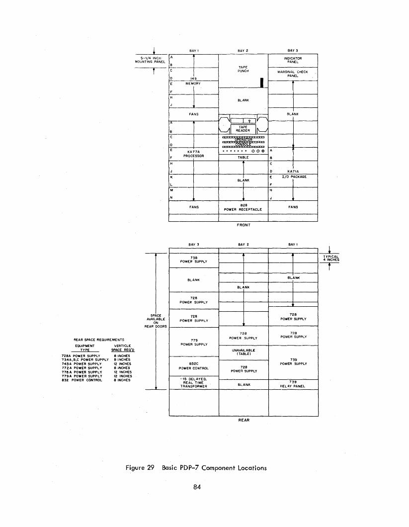
REAR SPACE REQUIREMENTS
EQUIPMENT TYPE
728A POWER SUPPLY 734A,B,C POWER SUPPLY 743A POWER SUPPLY 772 A POWER SUPPLY 778 A POWER SUPPLY 779A POWER SUPPLY 832 POWER CONTROL
VERTICLE SPACE REQ'D
8 INCHES 8 INCHES 12 INCHES 8 INCHES 12 INCHES 12 INCHES 8 INCHES
5-1/4 INCH MOUNTING PANEL
SPACE AVAILABLE
ON REAR DOORS
A
B
C
0
E
F
H
J
A-
B
C
0
E
F
H
J
K
L
M
N
BAY 1
149
MEMORY
FANS
KA77A PROCESSOR
FANS
BAY 3
738 POWER SUPPLY
BLANK
728 POWER SUPPLY
728 POWER SUPPLY
779 POWER SUPPLY
832C POWER CONTROL
--15 DELAYED, REAL TIME
TRANSFORMER
BAY 2
TAPE PUNCH
J BLANK
lr-\JI I ~ "In ~
TAPE lb! READER
: : : : : ~~if¥ : : : : : CONSOL . . ..... OOQ)
TABLE
1 BLiNK
1 828
POWER RECEPTACLE
FRONT
BAY 2
BLANK
728 POWER SUPPLY
UNAVAILABLE (TABLE)
728 POWER SUPPLY
BLANK
REAR
Figure 29 Basic PDP-7 Component Locations
84
A
B
C
0
E
F
H
J
BAY 3
INDICATOR PANEL
MARGINAL CHECK PANEL
BLANK
KA71A
I/O PACKAGE
FANS
BAY 1
BLANK
728 POwER SUPPLY
728 POWER SUPPLY
739 POWER SUPPLY
739 FlELAY PANEL
TYPICAL 4 INCHES
---r

BAY 0 BAY I
149 149
MEMORY MEMORY
FANS FANS
176 MEMORY PARITY CHECK
BLANK
BLANK KA77A
PROCESSOR BLANK
IJ3 DATA INTERRUPT
MULTlrEXER
FANS FANS
BAY 5 BAY 4
n6 POWER SUPPLY
726 726 POWER SUPPLY POWER SUPPLY
NOTE: IF 522 INTERFACE IS USED, TWO MOUNTING PANELS ARE REQUIRED
BAY 2 BAY 3 BAY 4
INDICATOR f PANEL TU55
DECTAPE TAPE PUNCH TRANSPORT
MARGINAL CHECK
~ I PANEL
138},39 ' TUt ALD CONVERTER DECTAPE
0 MULTILEXER TRAlpORT
34 DISPLAY OSCILLOSCOPE
AA03B
BLINK rll In MULTIPLEXER
I EXPANSION ~
172 AJOMATI'C
(FOR [U551
~1 TAPl It'--J READER
PRIORITY INTERRUPT gPiRATgR BLANK CONSOLE ....... oo~
TABLE
BLANK KA71A 550
177 EJENDED
I/O PACKAGE' DECTAPE CONTROL
ARITHMETIC I ELEIENT
828 FANS BLANK
POWER RECEPTACLE
FRONT
BAY 3 BAY 2 BAYI
738 POWER SUPPLY
72B POWER SUPPLY
728 728 POWER SUPPLY
POWER SUPPLY
728 726 POWER SUPPLY POWER SUPPLY
779 POWER SUPPLY
UNAVAILABLE (TABLE)
739 832C
728 POWER SUPPLY
POWER CONTROL POWER SUPPLY
-15 DELAYED, REAL 739 TIME TRANSFORMER RELAY PANEL
REAR
Figure 30 Typical PDP-7 System Component Locations
85
BAY 5
522 MAGNETIC TAPE
INTERFACE
520/521 MAGNETIC TAPE
INTERFACE
57A MAGNETIC
TAPE CONTROL
I
KB03 DEVICE SELECTOR EXPANSION
175
I. C. EXPANSION
BLANK
BAY 0
72B POWER SUPPLY

POWER REQUIREMENTS
The PDP-7 requires a source of 115v, 60-cps, single-phase power. On specic]l request, all equipment
can be factory wired for 50-cps and/or 220 to 250v power. The power source must maintain the nominal
voltage within ±100/0 under normal and transient load conditions. The electrical characteristics of in
dividual units are given in Table 5.
REMOVEABLE END PANEL.
C.ABLE ACCESS (TYPICAL FOR 3 C,o,BINETS)
CASTER SWlVAL RADIUS SWINGlfllG PLENUM DOORS 1:3)
3" ---.r---..----.~---.. t_ --4'''-_r---I-----+-------614" -------\--------.-j
7 II
343"2
27ik"
3" 8-4
-1--+-1-+ 29"
4 32
~--~-----+-----
---, I I L ____ J
+
+
+
,,~ 8
+
+
SWINGING DOORS (to)
LOAD POINT
REMOVEABLE END PANEL
SCREEN (TYPICAL FOR 3 CABINETS)
15" 14--------------------- 68ffi -------------------------~
FLOOR PLAN
Figure 31 Basic PDP-7 InstQllation Dimensions
CABLING REQUIREMENTS
All system power sources shou Id have 115v, 30-amp, Hubbel Twistlock flush receptac les (or their equiv
alent) to mate with equipment power cables.
86

Standard PDP-7
Core Memory Modu Ie 147
Memory Extension Control 148B**
Core Memory Module 149A
Priority Interrupt 172B
Data Interrupt MJltiplexer 173
Extended Arithmetic Element 1778
Dual DECtape Transport 555
DECtape Control 550
Magnetic Tape Transport 50
Automatic Magnetic Tape Control 57 A
Magnetic Tape Transport 570
Magnetic Tape Transport 545
Serial Drum 24
Oscilloscope Display 34F**
CRT Display 340
Slave Di splay 343
18-Bit Relay Buffer 140
A-D Converter 138E; 64Channel Multiplexer Control 139E
Data Communication System 630 (8 line)
Automatic Line Printer and Control 647
Card Reader and Control CROl B (100 cpm)
Typical Standard Cabinet Bay (empty)
REMARKS
Standard POP-7
Third bay has space for fhie panels of options.
Core ,AAemory Module 147
Fits in first bay of basic PDP-7.
12-16K memory requires minimum four-bay configuration.
TABLE 5 INSTALLATION DATA *
Dimensions (inches)
Height Width Depth (incl.
Panels tables)
69-1/8 61-3/4 61-1/4 36
-- -- -- ---- -- -- ---- -- -- 4
-- -- -- 2
-- -- -- 2
-- -- -- --12 19 17-1/2 ---- -- -- 4
69-1/8 22-1/4 27-1/16 ---- -- -- . 5
68 32-1/8 32-3/8 --69-1/8 22-1/4 27-1/16 --69-1/8 22-1/4 27-1/16 ---- -- -- --
69-1/8 42 51 1
69-1/8 22-1/4 51 ---- -- -- 2
-- -- -- 3
-- -- -- 2
52-57 56 30-1/4 --8-1/4 18 10 --
69-1/8 22-1/4 27-1/16 12
Core Memory Module 147 (continued)
20-32K memory requires five-bay configuration.
Draws no extra power.
Extended Arithmetic Element 1778
Fits in second bay of standard PDP-7.
Service Clearance Current (Amps)
Required (inches)
Cabinets Weight (Ibs.) Front
3 1150 8-3/4
-- 5 ---- -- ---- 80 ---- 60 ---- 40 ---- 40 ---- 65 2-1/4
-- 255 8-3/4
1 600 18-5/16
-- 281 8-3/4
1 850 30
1 400 18-5/8
1 I 500 _0 9
• -- -- --2 700 8-3/4
1 350 8-3/4
-- 40 ---- 50 ---- 40 --1 1350 24
1 25 --1 100 8-3/4
Dual DECtape Transport 555
Provision is made for installation of this unit in bay two of standard PDP-7.
Table model dimensions are given. Also can be mounted in two mounting panel positions.
DECtape Control 550
Mounted in standard bay.
Rear Nominal
14-7/8 17
-- ---- 0.5
-- 5.5
-- 1.5
-- 1
-- 1
-- 1.5
14-7/8 1.5
14-7/8 8
14-7/8 4
14-7/8 25
14-7/8 8
15 5 . -- 1
36 15
36 6
-- 1
-- 0.6
-- 1
26 13
6-5/8 0.57
14-7/8 --
Magneti c T ape Transport 570
Nonstandard cabinet.
Oscilloscope Display 34F
Surge
30
--7.5
7.5
2.75
2
2
3.2
3.2
12
6
38
12
8
2
20
10
2
0.77
2
19
1
--
Space for control logic is provided in basi c I/o package.
Oscilloscope RMS03 requires additional panel or may be mounted externally.
*This information is invalid for PDP-7 I s with serial numbers below 100. ** Mounted within basic computer
Heat Dissipation Power Dissipation (BTU/hr) (KW)
7150 2.1
-- --204 0.06
2040 0.6
612 0.18
408 0.12
408 0.12
585 0.172
585 0.172
2114 0.62
1564 0.460
9800 2.9
2114 0.62
1540 0.45
408 0.12
5900 1.73
2350 0.69
408 0.12
612 0.18
4080 1.2
5304 1.56
204 0.06
-- --
Card Reader & Control CR01 B
Table top model.
Requires one panel of additional cabinet space.
CRT Display 340
Requires one panel in bay three for cable connection to the external cabinet.
87
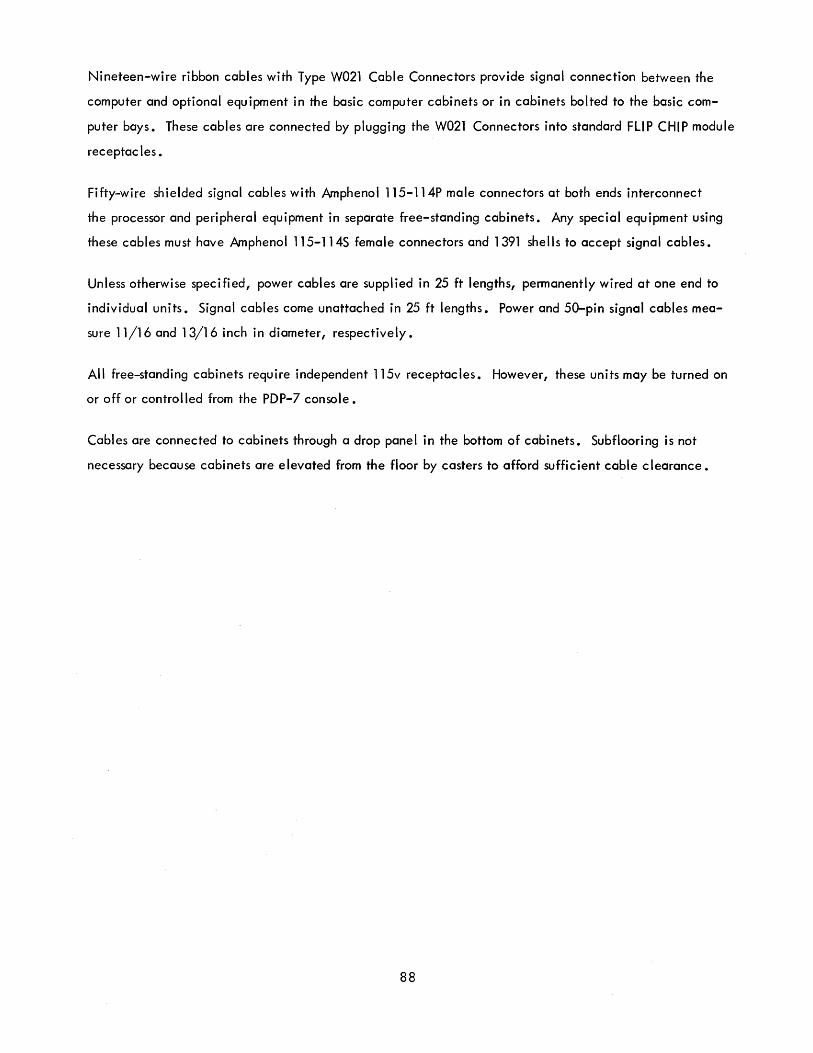
Nineteen-wire ribbon cables with Type W021 Cable Connectors provide signal connection between the
computer and optional equipment in the basic computer cabinets or in cabinets bolted to the basic com
puter bays. These cables are connected by plugging the W021 Connectors into standard FLIP CHIP module
receptac les •
Fifty-wire shielded signal cables with Amphenol 115-114P male connectors at both ends interconnect
the processor and peripheral equipment in separate free-standing cabinets. Any special equipment using
these cables must have Amphenol 115-1145 female connectors and 1391 shells to accept signal cables.
Unless otherwise specified, power cables are supplied in 25 ft lengths, permanently wired at one end to
individual units. Signal cables come unattached in 25 ft lengths. Power and 50-pin signal cables mea
sure 11/16 and 13/16 inch in diameter, respectively.
All free-standing cabinets require independent 115v receptacles. However, these units may be turned on
or off or controlled from the PDP-7 console.
Cabl es are connected to cabi nets through a drop pane lin the bottom of cabi nets. Subfloori ng is not
necessary because cabinets are elevated from the floor by casters to afford sufficient cable clearance.
88

APPENDIX 1
I·.
PDP-7 DEVICE S~LECTOR AND INFORMATION • . "" J,
COLLECTOR REQUIREMENTS FOR STANDARD OPTION,S
The standard d~vice selector on a PDP-7 with a tape reader, tape punch, and Tel~fype contains 12 spare
selector channe'ls. Each selector channel in a PDP-7 with a serial number o~er roo requires a' W1 03'
Device Selector module and a W640 Pulse Ampl ifier module (three circuits producing 40'O-nsec or 1":'!-'sec
pu Ises).
The standard information collector on a PDP-7 with a tape reader, tape punch; and' Teletype contains
5 spare inpuf.ch'annels. One Type 175 Information Collector Expansion 'option extends the st6ndard IC
by seven additional channels, making a total of 12 avai lable channels. The 1"75 requires one channel of
the standard. Ie;, the total number of availabl:e channels is 11 •
The following list specifies the number of DS and IC channels required for standard DEC options for the,
PDP-7. By using the following list, the need for DS or IC expansion ca~easily bedetermined~,for a;ny
system configuration containing standard DEC options. If required,these expansion ~I~~ents shou!~ be:
included in purchase orders and construction requisitions. In cases where only half a channel is required,
the remaining half is available for other options. Half channels are designated as 0.5L for the left half
(bits 0 through 8) or 0.5R for the right hal f (bits 9 through 17).
Option
Second Console Teletype and Control 649B
Memory Extension Control 148B
Memory Pari ty 176
Memory Increment 197
Memory Boundary Register KA70A
Automatic Priority Interrupt 172B
Data Interrupt Mu Itiplexer 173
Extended Arithmetic Element 177B
DECtape Control 550
Automatic Magnetic Tape Control 57 A
Serial Drum 24
Incremental Plotter and Control 350
89

Option OS Channels IC Channels
asci lIoscope Display 34F 2 0
Precision CRT Display 300 3 0
Symbol Generator 33 (for 300) 1 0
Precision Incremental Display 340 4 2
Subroutine Option 347 (for 340) 4 4
Character Generator 342 (for 340) 0 0
Slave Display 343 (for 340) 0 0
Photomultiplier Light Pen 370 0
Relay Buffer 140 0
Analog-to-DigitaIConverter 138E 1
General Purpose Multiplexer 139E 2 O.5R
Digital-to-Analog Converter MOl A 3 0
Data Communications System 630 62 O.5R
Automatic Line Printer 647 2 0
Card Reader and Control CROT B
Card Reader and Control· CR02A
Interprocessor Buffer 195 2
90

5119
ma·aD D EQUIPMENT CORPORATION MAYNARD,MASSACHUSETTS
Printed in U.S.A. 15 -3/66