interface phenomena in organic electronics
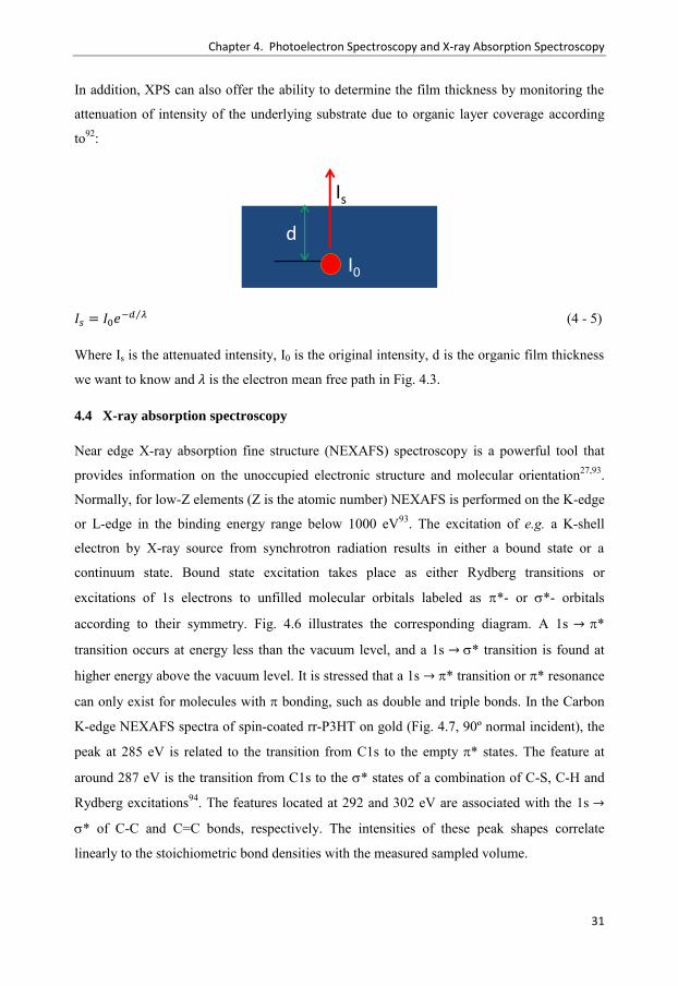
TRANSCRIPT
I
Linköping Studies in Science and Technology
Dissertation No. 1658
Interface Phenomena in Organic Electronics
Surface Physics and Chemistry Division
Department of Physics, Chemistry and Biology (IFM)
Linköping University, Sweden
2015 Linköping

II
Copyright @ Qinye Bao 2015, unless otherwise noted
Interface Phenomena in Organic Electronics
Qinye Bao
ISBN: 978-91-7519-077-8
ISSN: 0345-7524
Linköping Studies in Science and Technology
Dissertation No. 1658
Printed by LiU-Tryck, Linköping, Sweden, 2015

III
Abstract
Organic electronics based on organic semiconductors offer tremendous advantages compared to
traditional inorganic counterparts such as low temperature processing, light weight, low
manufacturing cost, high throughput and mechanical flexibility. Many key electronic processes in
organic electronic devices, e.g. charge injection/extraction, charge recombination and exciton
dissociation, occur at interfaces, significantly controlling performance and function.
Understanding/modeling the interface energetics at organic-electrode/organic-organic heterojunctions
is one of the crucial issues for organic electronic technologies to provide a route for improving device
efficiency, which is the aim of the research presented in this thesis.
Integer charge transfer (ICT) states pre-existed in the dark and created as a consequence of Fermi
level equilibrium at donor-acceptor interface have a profound effect on open circuit voltage in organic
bulk heterojunction photovoltaics. ICT state formation causes vacuum level misalignment that yields
a roughly constant effective donor ionization potential to acceptor electron affinity energy difference
at the donor-acceptor interface, even though there is a large variation in electron affinity for the
fullerene series. The large variation in open circuit voltage for the corresponding device series instead
is found to be a consequence of trap-assisted recombination via integer charge transfer states. Based
on the results, novel design rules for optimizing open circuit voltage and performance of organic bulk
heterojunction solar cells are proposed.
Doping and insertion of interlayer are two established methods for enhancing charge
injection/extraction properties at organic-electrode interface. By studying the energy level alignment
behavior at low to intermediate doping levels for molecule-doped conjugated polymer/electrode
interfaces, we deduce that two combined processes govern the interface energetics: (i) equilibration of
the Fermi level due to oxidation (or reduction) of polymer sites at the interface as per the ICT model
and (ii) a double dipole step induced by image charge from the dopant-polymer charge transfer
complex that causes a shift of the work function. Such behavior is expected to hold in general for low
to intermediate level doped organic semiconductor systems. The unified model is further extended to
be suitable for conjugated electrolyte/electrode interfaces, revealing the design rules for achieving the
smallest charge injection/extraction barrier for both thin tunneling and thick charge transporting
conjugated electrolyte interlayers.
To probe into the energy level spatial extension at interfaces, we employ the original approach of
building and characterizing multilayers composed of a well-defined number of polymer monolayers
with the Langmuir-Shäfer method to control polymer film uniformity and thicknesses, avoiding the
problems associated with spin-coating ultrathin films. The disordered/amorphous films feature smaller,

IV
and in fact negligible, energy level bending compared to the more well-ordered films, in contradiction
with existing models. It is found that that energy level bending depends on the ICT state distribution
rather than the density of states of the neutral polymer chains in relation to the Fermi energy, thus
taking into account the Coulomb energy associated with charging the polymer chain and transferring a
charge across the interface. Based on this work, a general model for energy level bending in absence
of significant doping of conjugated polymer films is proposed.
Organic semiconductors are sensitive to ambient atmosphere that can influence the energetics. The
degradation effects of common PCBM film induced by oxygen and water are found to be completely
different. Upon exposure to oxygen, the work function is down-shifted by ~ 0.15 eV compared to the
ICT curve of the pristine PCBM film, originating from the weak interaction between the fullerene part
of PCBM and oxygen, and this can be reversed by thermal treatment in vacuum. The down-shift in
energetics will cause a loss in open circuit voltage at electrode interface, but aids free charge
generation at donor-acceptor interface. Upon exposure to water, there is irreversible extensive
broadening and bleaching of the valence electronic structure features as well as a substantial decrease
of work function and ionization potential, severely degrading the transport properties.
Overall, the research results in this thesis thus give a deeper understanding of interface phenomena in
organic electronics, especially regard to organic solar cells, aimed to further improve the device
operation efficiency and lifetime.

V
Populärvetenskaplig Sammanfattning
Organisk elektronik baserade på organiska halvledare erbjuder stora fördelar jämfört med traditionella
oorganiska material såsom: tillverkning vid låg temperatur, låg vikt, låg tillverkningskostnader, hög
produktionstakt och mekanisk flexibilitet. Många viktiga elektroniska processer i organiska
elektronik-komponenter, t.ex. laddningsinjektion, laddningsrekombination och excitonseparation,
inträffar vid gränsytor och påverkar i hög grad komponenternas funktion och prestanda. Förståelse
och modellering av energinivåer vid organisk-elektrod/organisk-organisk heterogena gränsytor är en
av de viktigaste frågorna för organisk elektronisk teknik för att driva fram förbättringar inom
komponenteffektivitet, vilket är syftet med forskningen som presenteras i avhandlingen. Speciell
emfas har lagts på studier av organiska material och gränsytor med relevans för organiska solceller,
men många av resultaten har även tillämpningar inom organisk elektronik i stort.
I så-kallade organiska bulk-heterogena solceller, där en blandning av donator- och acceptormaterial i
ett lager absorberar ljus och omvandlar ljuset till ström, anses energiskillnaden mellan den hål-
transporterande nivån i donatormaterialet och den öppenkretsspänningen som solcellen kan generera.
Den faktiska öppenkretsspänningen blir dock aldrig så hög på grund av interna förluster, vilka måste
minimeras för att uppnå maximal effektivitet i energiomvandlingen. I sen studie visar vi at
laddningsöverföring som förekommer i mörker och skapas som en följd av Fermi-nivån jämvikt vid
donator-acceptor-gränsytorna i blandlagret har en djupgående effekt på öppenkretsspänningen. För en
serie av acceptormaterial i kombination med en donator visar vi att laddningsöverföring orsakar ett
potentialsteg vid gränsytorna som ger en i stort sett konstant energiskillnaden mellan
donatormaterialets hål-transporterande nivå och acceptorns elektrontransporterande nivå, även om det
finns en stor variation i elektronaffinitet för acceptorserien. Den stora variationen i
öppenkretsspänning visar sig istället vara en konsekvens av laddningsrekombination via tillstånd
skapade av den ”mörka” laddningsöverföringen. Baserat på resultaten från vår studie kan vi föreslå
nya regler för att optimera öppenkretsspänning och prestanda av organiska heterogen bulksolceller,
vilket framgångsvist testas på en serie av organiska donator- och acceptormaterial.
Doping och användning av ett mellanskikt är två etablerade metoder för att förbättra
laddningsöverföring vid organisk-elektrod gränsytor och minimera spänningsförluster. Genom att
studera gränsytors elektronstruktur vid låga till medelhöga dopningsnivåer för molekyl-dopade
konjugerad polymer/elektrod-gränsytor, kan vi visa att två kombinerade processer styr gränsytornas
energinivåupplinjering: (i) jämvikt av Fermi-nivån genom oxidation (eller reduktion) av polymerer
vid gränsytan enlig vår generella modell for laddningsöverföring och (ii) ett dubbel-dipolsteg
inducerad av spegelladdning från dopmolekyl-polymer laddningsöverföringskomplexet som orsakar
ett potentialsteg vid gränsytan. Ett sådant beteende förväntas hålla i allmänhet för låga till medelhögt

VI
dopade organiska halvledarsystem. Den nya modellen utvidgas ytterligare för att beskriva konjugerad
elektrolyt/elektrod gränssnitt, avslöjar regler för att minimera barriärer för
laddningsinjektion/extraktion, både för tunna (tunnling) och tjocka (laddningstransport) konjugerade
elektrolytmellanskikt.
Ett annan fundamental frågeställning är hur långt ifrån en gränsyta ett potentialfall inducerat av
laddningsöverföring sträcker sig. Här använder vi en ny strategi baserad på att bygga och
karakterisera multilager med väldefinierade antal polymermonolager deponerade via Langmuir-Shäfer
metoden och därmed undvika de oregelbundna och dåligt definierade filmer som är förknippade med
spin-beläggning eller förångning av ultratunna lager. I kontrast mot de existerande modellernas
förväntningar, så visar oordnade/amorfa filmer mindre, och i själva verket försumbar, utsträckning av
laddningsöverföringsområdet, än de mer välordnade filmerna. Resultaten följer väl vår modell för
energinivåupplinjering och representerar de första mätningarna av energinivåupplinjering i
konjugerade polymerer på väl definierade ultratunna prover.
Organiska halvledare kan vara känsliga för exponering mot luft, då kemiska reaktioner med syre eller
vatten kan påverka de laddningstransporterande energinivåerna och därmed komponentfunktion. En
vanligt använd acceptormolekyl inom organiska solceller, PCBM, studeras för att klarlägga effekten
av syre- och vattenexponering. Våra studier visar att syre och vatten påverkar PCBM lager på helt
olika sätt. Vid exponering för syre skiftas arbetsfunktionen nedåt med ~ 0.15 eV jämfört med ”ren”
PCBM film, vilket kan ha en negativ effekt på öppenkrets-spänning beroende på val av elektrod, men
och andra sidan förbättra generering av fria laddningar vid donator/acceptor gränsytor. Väkelverkan
mellan syre och PCBM i filmen är dock svag och effekten kan vändas genom termisk behandling i
vakuum. Vatten reagerar kraftigt med PCBM lagret med omfattande förändring av elektronstruktur
och minskning av arbetsfunktionen, till skada för komponentfunktion. Denna interaktion är
irreversibel så PCBM bör därmed skyddas från vatten under samtliga delar av tillverkningsprocessen
och under komponentanvändning.
VII
List of Publications Included in this Thesis
1. Trap-Assisted Recombination via Integer Charge Transfer States in Organic Bulk
Heterojunction Photovoltaics
Q. Y. Bao, O. Sandberg, D. Dagnelund, S. Sanden, S. Braun, H. Aarnio, X. J. Liu, W. M.
Chen, R. Österbacka, and M. Fahlman
Advanced Functional Materials, 2014, 24, 6309
2. Oxygen- and Water-Based Degradation in [6, 6]-Phenyl-C61-Butyric Acid Methyl
Ester (PCBM) Films
Q. Y. Bao, X. J. Liu, S. Braun, and M. Fahlman
Advanced Energy Materials, 2014, 4, 1301272
3. The Energetics of the Semiconducting Polymer-Electrode Interface for Solution-
Processed Electronics
Q. Y. Bao, S. Fabiano, M. Andersson, S. Braun, Z. Y. Sun, X. Crispin, M. Berggren, X. J.
Liu, and M. Fahlman
(Submitted)
4. Energetics at Doped Conjugated Polymer/Electrode Interfaces
Q. Y. Bao, X. J. Liu, S. Braun, F. Gao, and M. Fahlman
Advanced Materials Interfaces, 2015, 2, 1400403
5. Regular Energetics at Conjugated Electrolyte/Electrode Modifier for Organic
Electronics and Their Implications of Design Rules
Q. Y. Bao, X. J. Liu, E. G. Wang, J. F. Fang, F. Gao, S. Braun, and M. Fahlman
(Submitted)
6. Effects of Ultraviolet Soaking on Surface Electronic Structures of Solution
Processed ZnO Nanoparticle Films in Polymer Solar Cells
Q. Y. Bao, X. J. Liu, Y. X. Xia, F. Gao, L. D. Kauffmann, O. Margeat, J. Ackermann,
and M. Fahlman
Journal of Materials Chemistry A, 2014, 2, 17676

VIII
List of Publications not Included in this Thesis
1. Correlation Between the Electronic Structures of Transition Metal Oxide-Based
Intermediate Connectors and the Device Performance of Tandem Organic Light-Emitting
Devices
Q. Y. Bao, J. P. Yang, Y. Xiao, Y. H. Deng, S. T. Lee, Y. Q. Li, and J. X. Tang
Journal of Materials Chemistry, 2012, 21, 17476
2. Interfacial Electronic Structures of WO3-Based Intermediate Connectors in Tandem
Organic Light-Emitting Diodes
Q. Y. Bao, J. P. Yang, J. X. Tang, Y.Q. Li, C. S. Lee, and S. T. Lee
Organic Electronics, 2010, 11, 1578
3. Electronic Structures of MoO3-Based Charge Generation Layer for Tandem Organic
Light-Emitting Diodes
Q. Y. Bao, J. P. Yang, Y.Q. Li, and J. X. Tang
Applied Physics Letter, 2010, 97, 063303
4. Role of Thick-Lithium Fluoride Layer in Energy Level Alignment at Organic/Metal
Interface: Unifying Effect on High Metallic Work Functions
Z. Y. Sun, S. W. Shi, Q. Y. Bao, X. J. Liu, and M. Fahlman
Advanced Materials interface, 2015, 1400527
5. New Bulk-Heterojunction System for Efficient High-Voltage and High-Fill Factor
Solution-Processed Fullerene-Free Organic Photovoltaics
Z. Tang, B. Liu, A. Melianas, J. Bergqvist, W. Tress, Q. Y. Bao, D.P. Qian, O. Inganäs,
and F. L. Zhang
Advanced Materials, 2015, DOI: 10.1002/adma.201405485
6. Morphological Control for Highly Efficient Inverted Polymer Solar Cells via the
Backbone Design of Cathode Interlayer Materials
W. J. Zhang, Y. L. Wu, Q. Y. Bao, F. Gao, and J. F. Fang
Advanced Energy Materials, 2014, 4, 1400359
IX
7. Interplay of Optical, Morphological and Electronic Effects of ZnO Optical Spacers in
Highly Efficient Polymer Solar Cells
S. B. Dkhil, D. Duché, M. Gaceur, A. K.Thakur, F. B. Aboura, L. Escoubas, J. J. Simon,
A. Guerrero, J. Bisquert, G. G. Belmonte, Q. Y. Bao, M. Fahlman, C. V. Ackermann, O.
Margeat, and J. Ackermann
Advanced Energy Materials, 2014, 4, 1400805
8. Improving Cathodes with a Polymer Interlayer in Reversed Organic Solar Cells
Z. Tang, W. Tress, Q. Y. Bao, M. J. Jafari, J. Bergqvist, T. Ederth, M. R. Andersson, and
O. Inganäs
Advanced Energy Materials, 2014, 4, 1400643
9. A Renewable Biopolymer Cathode with Multivalent Metal Ions for Enhanced Charge
Storage
S. Admassie, A. Elfwing, E. W. H. Jager, Q. Y. Bao, and O. Inganäs
Journal of Material Chemistry A, 2014, 2, 1974
10. Solution-Processable Graphene Oxide as an Efficient Hole Injection Layer for High
Luminance Organic Light-Emitting Diodes
S. W. Shi, V. Sadhu, R. Moubah, G. Schmerber, Q. Y. Bao, and S. Ravi P. Silva
Journal of Materials Chemistry C, 2013, 1, 1708
11. Hybrid Intermediate Connector for Tandem OLEDs with the Combination of MoO3-
Based Interlayer and P-Type Doping
J. P. Yang, Q. Y. Bao, Y. Xiao, Y. H. Deng, Y. Q. Li, S. T. Lee, J. X. Tang
Organic Electronics, 2012, 13, 2243
12. Role of Transition Metal Oxides in Charge Recombination Layer Used in Tandem
Organic Photovoltaic Cells
J. Li, Q. Y. Bao, H. X. Wei, Z. Q. Xu, J. P. Yang, Y. Q. Li, S. T. Lee, and J. X. Tang
Journal of Materials Chemistry, 2012, 22, 6285
13. Mechanism of Cs2CO3 as an N-Type Dopant in Organic Electron-Transport Film
Y. Cai, H. X. Wei, J. Li, Q. Y. Bao, X. Zhao, S. T. Lee, Y. Q. Li, and J. X. Tang
X
Applied Physics Letter, 2011, 98, 123303
14. Light Out-Coupling Enhancement of Organic Light-Emitting Devices with Microlens
Array
J. P. Yang, Q. Y. Bao, Z. Q. Xu, Y. Q. Li, J. X. Tang, and S. Shen
Applied Physics Letter, 2010, 97, 223303
15. Catalytic Epoxidation of Stilbene with FePt@Cu Nanowires and Molecular Oxygen
L. Hu, L. Y. Shi, H. Y. Hong, M. Li, Q. Y. Bao, J. X. Tang, J. F. Ge, J. M. Lu, X. Q. Cao,
and H. W. Gu
Chemical Communication, 2010, 42, 8591
16. Book chapter: “Application of Transition Metal Oxides in Tandem Organic
Optoelectronics: Energetics and Device Physics” in New Developments in Metal Oxides
Research, Eds. I. Nagy and A. Balogh, Nova Science Publishers, New York, USA (2013),
ISBN: 978-1-62808-149-7.
Q. Y. Bao, Y. Q. Li and J. X. Tang

XI
Conferences
Energetics at molecule-doped polymer/electrode interface for photovoltaic cells
Q. Y. Bao, X. J. Liu, S. Braun, and M. Fahlman
Materials Research Society (MRS), 2015, April 6-10, San Francisco, California, USA (Talk)
Trap-assisted recombination via integer charge transfer states in organic bulk heterojunction
photovoltaics
Q. Y. Bao, O. Sandberg, D. Dagnelund, S. Sanden, S. Braun, H. Aarnio, X. J. Liu, W. M.
Chen, R. Österbacka, and M. Fahlman
Materials Research Society (MRS), 2014, November 30-December 5, Boston, Massachusetts,
USA (Talk)
Integer charge transfer state as a promising approach for optimizing organic solar cell
efficiency
Q. Y. Bao, O. Sandberg, S. Sandén, S. Braun, H. Aarnio, X. J. Liu, R. Österbacka, and M.
Fahlman
International Conference for Science and Technology of Synthetic Metals (ICSM), 2014,
June 30-July 5, Turku Finland (Talk)
Oxygen- and water-based degradation mechanism in PCBM films
Q. Y. Bao, X. J. Liu, S. Braun, and M. Fahlman
Materials Research Society (MRS), 2013, December 1-6, Boston, Massachusetts, USA (Talk)
Optimizing organic solar cell efficiency using the integer charge transfer model
Q. Y. Bao, X. J. Liu, D. Degnelund, S. Braun, and M. Fahlman
Hybrid and Organic Photovoltaics (HOPV), 2014, May 11-14, Lausanne, Switzerland (Poster)
Electronic structure of solution processed donor-acceptor heterojunctions: the effect of dark
state interface dipole and blend de-mixing
Q. Y. Bao, X. J. Liu, S. Braun, S. W. Shi, and M. Fahlman
Materials Research Society (MRS), 2013, December 1-6, Boston, Massachusetts, USA
(Poster)

XII

XIII
Acknowledgements
First of all, I would like to express my sincere thanks to my supervisor, Prof. Mats Fahlman
for giving me the precious opportunity to pursue my Ph.D study in the Surface Physics and
Chemistry Division. A great deal of time and efforts has been devoted to supervision, help,
support and encouragement during my past 4 years. I want to say that I very enjoy the open
research atmosphere in your group, and I learned a lot from you, which will be the valuable
asset in my future career.
Great gratitude also goes to my co-supervisor, Dr. Xianjie Liu and Dr. Slawomir Braun, who
not only helped me with UHV systems, but also shared me with their abundant scientific
knowledge.
I would also thank all of the members of the Surface Physics and Chemistry Division, past
and present, for assistance in the lab. Special acknowledgments to our administrator Kerstin
Vestin for all the help with practical things.
Moreover, I am grateful to all collaborators and co-authors to the papers.
I want as well to thank all my Chinese friends in Linköping, not explicitly mentioned here.
Finally, I would like express my deepest appreciation and thanks to my wife Jing Zhang, my
parents, my sister and her family. It is you to always support me all the years.

XIV
Abbreviations
EF Fermi level
VL Vacuum level
Δ Vacuum level potential step
HOMO Highest occupied molecular orbital
LUMO Lowest unoccupied molecular orbital
IP Ionization potential
EA Electron affinity
ICT+ Positive integer charge transfer state
ICT- Negative integer charge transfer state
UHV Ultra high vacuum
PES Photoelectron spectroscopy
XPS X-ray photoelectron spectroscopy
UPS Ultraviolet photoelectron spectroscopy
NEXAFS Near edge X-ray absorption fine structure
OSC Organic semiconductor
OPV Organic photovoltaic
BHJ Bulk heterojunction
XV
Contents
Abstract .................................................................................................................................. III
Populärvetenskaplig Sammanfattning .................................................................................. V
List of Publications Included in this Thesis ....................................................................... VII
List of Publications not Included in this Thesis .............................................................. VIII
Conferences ........................................................................................................................... XI
Acknowledgements ............................................................................................................ XIII
Abbreviations ..................................................................................................................... XIV
Contents ................................................................................................................................ XV
Chapter 1. General Introduction ........................................................................................... 1
Chapter 2. Basic Properties of Conjugated Polymer ........................................................... 5
2.1 Electronic structure ..................................................................................................................... 5
2.2 Charge carrier .............................................................................................................................. 9
Chapter 3. Interface Energetics in Organic Electronics ................................................... 13
3.1 Interface categories ................................................................................................................... 13
3.2 Weakly interacting interfaces .................................................................................................... 14
3.3 Integer Charge Transfer model ................................................................................................. 15
3.3.1 Basics of the integer charge transfer model ........................................................................ 15
3.3.2 Organic-electrode interfaces ............................................................................................... 18
3.3.3 Donor-acceptor interfaces ................................................................................................... 18
3.4 Hybridized interfaces ................................................................................................................ 20
3.5 Strongly interacting interfaces .................................................................................................. 22
Chapter 4. Photoelectron Spectroscopy and X-ray Absorption Spectroscopy ............... 25
4.1 Basics of photoelectron spectroscopy ....................................................................................... 25
4.2 Ultraviolet photoelectron spectroscopy (UPS).......................................................................... 28
4.3 X-ray photoelectron spectroscopy (XPS) ................................................................................. 30
4.4 X-ray absorption spectroscopy .................................................................................................. 31
Chapter 5. Operation Principles of Organic Solar Cell .................................................... 35
Chapter 6. Summary of Papers Included in the Thesis ..................................................... 39
6.1 Paper I ....................................................................................................................................... 40
6.2 Paper II ...................................................................................................................................... 42
6.3 Paper III .................................................................................................................................... 43

XVI
6.4 Paper IV .................................................................................................................................... 45
6.5 Paper V...................................................................................................................................... 46
6.6 Paper VI .................................................................................................................................... 47
Chapter 7. Future Outlook................................................................................................... 49
References ............................................................................................................................... 51
Publications ............................................................................................................................ 57
Chapter 1. General Introduction
1
Chapter 1. General Introduction
The field of organic electronics is rapidly growing based on -conjugated organic
semiconductors (OSCs), i.e. small molecules and polymers, with applications in e.g. thin-film
transistors (OTFTs)1, light emitting diodes (OLEDs)2, photovoltaic cells (OPVs)3,
photodetectors4, memory cells5, laser6 and spintronics7. The interest is mainly a function of a
wide variety of potential advantages of OSCs that are hard to achieve in inorganic
components, such as low temperature processing, light weight, low manufacturing cost, high
throughput, mechanical flexibility, tunable optical and electronic properties through synthesis.
To date, OLEDs have found their way into commercial products featuring remarkable color
resolution displays in, e.g. cell phones and televisions, whereas OTFTs and OPVs are still
waiting for a commercial breakthrough. Especially, the development of OPVs as a promising
renewable-energy source has intensified and energy conversion efficiencies of ~ 11% have
been demonstrated8,9. All such OSC-based devices mentioned above are deposited as thin
film architectures and thus contain several interfaces, metal-organic and/or organic-organic,
that significantly determine performance and lifetime. Many key electronic processes as
charge injection/extraction, charge recombination and exciton dissociation occur at
interfaces10-12. In fact, even charge transport can be seen as a special injection behavior across
organic-organic junction since the charges are localized on molecules13. Therefore, one of the
crucial issues for organic electronic technologies is to understand and predict interface
energetics and its effect on device operational efficiency14-16.
Many studies find that the interface phenomena of weakly interacting interface follow the so-
called integer charger transfer (ICT) model where heterojunctions are characterized by weak
van der Waals intermolecular bonding17-19. The cases for the type of interfaces exist in metal-
organic and organic-organic junctions prepared by solution process of polymer under ambient
conditions and by thermal evaporation of small molecule under vacuum conditions. The
relation between the original Fermi level of a surface and the pinning energies of OSCs are
divided into three regimes considering oxidization/reduction of segments (molecules)
adjacent to the interface: (i) Fermi level is pinned at negative ICT density of states with an
up-shift potential step, (ii) Vacuum levels align, (iii) Fermi level is pinned at positive ICT
density of states with a down-shift potential step19,20. The size of potential step scales with the
difference between equilibrium ionization potential (iii)/electron affinity (i) of OSCs at
Chapter 1. General Introduction
2
interface (EICT+/-) and the work function of the underlying substrate, which is originated from
spontaneous charge transfer across interface via tunneling.
Bulk heterojunction OPV device is a main topic of the thesis, excitons created upon photon
absorption in the active layer diffuse into the donor-acceptor interface region where they are
transformed into charge transfer excitons, and subsequently dissociated into free charges that
will finally be transported into electrodes. To put it simply, the lowest unoccupied molecular
orbital (LUMO) energy level offset at donor-acceptor interface should be large enough to
overcome the exciton binding energy to assist the transformation, but if the offset is too large,
loss of open circuit voltage will occur21. Furthermore, a potential step at donor-acceptor
interface can enhance the percentage of charge transfer excitons transformed into free
chargers that contribute to short circuit current, while simultaneously decrease open circuit
voltage22,23. The energetics at active layer-electrode interface also are of tremendous
importance because barriers toward the charge extraction can diminish open circuit voltage,
and surface states at the electrode can lead to reduce overall efficiency due to trap-assisted
recombination24. It is clear that the energetics at both donor-acceptor and electrode interfaces
in OPVs should be optimized so as to minimize device efficiency loss.
Photoelectron spectroscopy including ultraviolet and X-ray photoelectron spectroscopy is a
successful surface science technique to map out energetics at interface and surface chemical
states with advantages of being relatively non-destructive to OSCs and extremely surface
sensitive25,26. The technique enables direct probing of the work function, the vertical
ionization potential, the occupied density of states, the simplified hole injection barrier and
the vacuum level shift upon forming an interface, as well as the pinning energies in
combination with the ICT model that governs the weakly interacting interface energetics. For
such measurements, ultraviolet light is typically used, whereas x-ray is used for tracking the
possible chemical interaction at interface and the change of chemical states at the surface.
Near edge X-ray absorption fine structure spectroscopy yields information about the
unoccupied electronic structure and the molecular orientation that may significantly affect the
interface energetics27.
In this thesis, six papers regarding the issues mentioned above are included. Paper I proposes
new design rules for donor-acceptor interfaces for optimizing open circuit voltage and overall
performance of OPVs, in fact enabling not just efficient screening of OSC donor and acceptor
materials but also in silico design thereof. Paper II reveals the completely different
Chapter 1. General Introduction
3
degradation mechanisms of interface energetics of PCBM-electrode interface caused by
oxygen and water. Paper III proposes a general model for energy level bending in absence of
significant doping of conjugated polymer films, showing experimental results that overturn
some of the recent models. Papers IV and V are devoted to developing a universal model for
handling interface energetics that simultaneously treats doped conjugated polymers and
conjugated electrolyte/electrode interfaces, which are two established methods for improving
charge injection/extraction efficiency. Paper VI presents the effect of the environment, e.g.
UV-light soaking under different conditions, on surface electronic structures of ZnO
nanoparticle interlayer films and the OPV performance.
Following the general introduction of Chapter 1 in this thesis, a short description of basic
properties of conjugated polymer is given in Chapter 2. Chapter 3 in detail provides reader
with description of various interface energetics in organic electronics depending on the
strength of interface interaction from weakly interacting, hybridization to strongly interacting
interfaces. The ICT model applied in weakly interacting interfaces existing in OPVs is
discussed. In Chapter 4, the experimental techniques of photoelectron spectroscopy and X-
ray absorption are presented. The operation principles of OPVs are included in Chapter 5.
Chapter 6 summarizes the papers included in this thesis, and the further outlook is given in
Chapter 7.

4
Chapter 2. Basic Properties of Conjugated Polymer
5
Chapter 2. Basic Properties of Conjugated Polymer
2.1 Electronic structure
Conventional polymers, plastics, were for a long time after their discovery viewed as
insulators only. The concept of electrically conducting polymer can date back to the
molecular crystal research in the 1960s, and later, in 1970s the science of -conjugated
polymer was established when it was found through successful synthesis and use of doping
that polyacetylene can have metallic-like electrical conductivity28,29. Since then, intense
attention has been paid to this type of organic materials, leading to their significant
application in devices, such as field-effect transistors and integrated circuits1,30, light-emitting
diodes2, photovoltaic cells3, detectors4, memories5, solid-state lasers6 and spintronics7 with
various potential advantages compared to the inorganic counterparts such as high throughput,
cheap manufacturing cost, light weight, and mechanical flexibility.
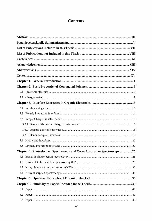
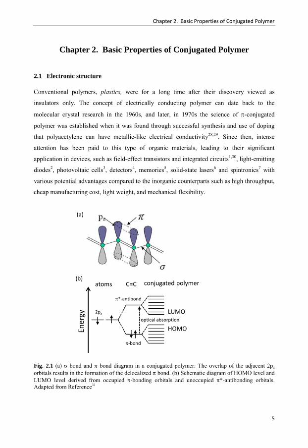
Fig. 2.1 (a) bond and bond diagram in a conjugated polymer. The overlap of the adjacent 2pz orbitals results in the formation of the delocalized bond. (b) Schematic diagram of HOMO level and LUMO level derived from occupied -bonding orbitals and unoccupied *-antibonding orbitals. Adapted from Reference31
Ener
gy 2pz
*-antibond
-bond
HOMO
LUMO
atoms C=C conjugated polymer
(a)
(b)
optical absorption

Chapter 2. Basic Properties of Conjugated Polymer
6
Conjugated polymers consist mainly of a continuous network, often long-chain, of organic
molecules with a series of alternating double and single bonds between the adjacent carbon
atoms, which in fact is what enables the semiconducting or conducting properties (Fig. 2.1a).
Because the electronic structure configuration of carbon is 1s22s22p2 and the 1s core level
does not contribute to the chemical bonding, the electron conjugation results in the so-called
sp2 hybridized state yielding three covalent bonds (2s, 2px and 2py) with neighboring
carbon and hydrogen atoms within one co-plane. The remaining 2pz orbital is free to overlap
with the corresponding one on a neighboring atom resulting in the formation of another
chemical bond known as the bond. The -bonds induce states that can be delocalized along
the polymer chain. The highest occupied molecular orbital (HOMO) similar to the valence
band in inorganic materials and the lowest unoccupied orbital (LUMO) analogous to the
conduction band are derived from the occupied -bonding orbitals and the unoccupied *-
antibonding orbitals, respectively32,33. The frontier electronic bands are separated by the -
bond-antibonding gap, see Fig. 2.1b, which accounts for the optical absorption of low energy
excitation and semiconductor behavior.
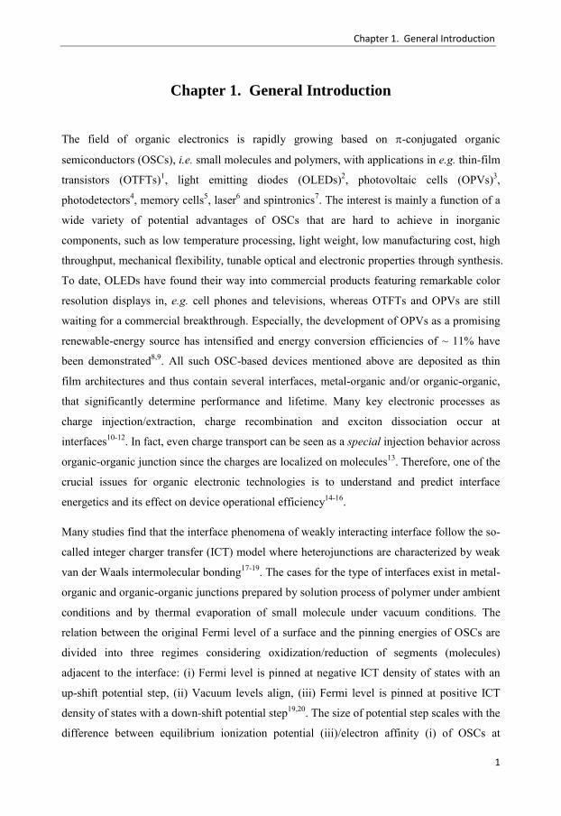
Fig. 2.2 (a) Representation of the energy Gaussian distribution of the HOMO and LUMO levels. Adapted from Reference34 (b) IP and EA distribution in related to the vacuum level depending on the intermolecular order and the nature of surrounding chains in conjugated polymer film. Energy differences between HOMO/LUMO and IP/EA originate from the relaxation process.
Energy bands in a solid originate from orbital overlap amongst its large number of particles
and a well-defined crystal lattice structure. Polymer chains aggregate in films via weak van
der Waals force which holds them together, making them “soft” materials. In practice, the
Vacuum level
LUMO
EA distribution
IP distribution
HOMO
Conjugated polymer film
(a) (b)
Chapter 2. Basic Properties of Conjugated Polymer
7
real polymer films are seldom single crystal films, and are instead amorphous35, at best
polycrystalline36 or the mixture of well ordered (polycrystalline) regions and disordered
(amorphous) regions37, which means that the concept of energy bands does not generally hold.
The electronic structures of polymer films instead typically are defined by localized states.
Due to the variations in the conjugation lengths and in the interaction energetics of
conjugated polymers, there is a distribution of the density of states of HOMO and LUMO,
often modeled as following a Gaussian shape (Fig. 2.2a). The ionization potential (IP) is
defined as minimum amount of energy required to remove an electron from a neutral polymer
chain to form a fully relaxed positive ion, and the electron affinity (EA) is maximum amount
of energy released when an electron is added to a neutral chain form a fully relaxed negative
ion38.
Since the IP and EA derived from these molecular orbitals also largely depend on the
intermolecular order and the nature of surrounding chains, in conjugated polymer films, a
broad distribution of IP/EA occurs for each orbital39 (Fig. 2.2b). The energy gap is then
defined by the upper edge of the IP energy distribution and the lower edge of the EA energy
distribution, those edges becoming the film IP and EA respectively. There are consequently
then per definition no gap states in absence of doping or synthetic defects, which is
fundamentally different from a single crystal. It is noted that IP (EA) is equal to HOMO
(LUMO) only if there is no electronic and no nuclear relaxation process withdrawing
(receiving) an electron40. The frontier part of the IP and EA is typically modeled as being
either Gaussian or exponential, and the most easily oxidized/reduced states in the IP/EA
distribution are typically then referred to as tail states. In fact, the position in the IP/EA that
separates the “tail” states from the “proper” states are not easily defined except for a ~ perfect
single-crystal organic semiconductor film.
Chapter 2. Basic Properties of Conjugated Polymer
8
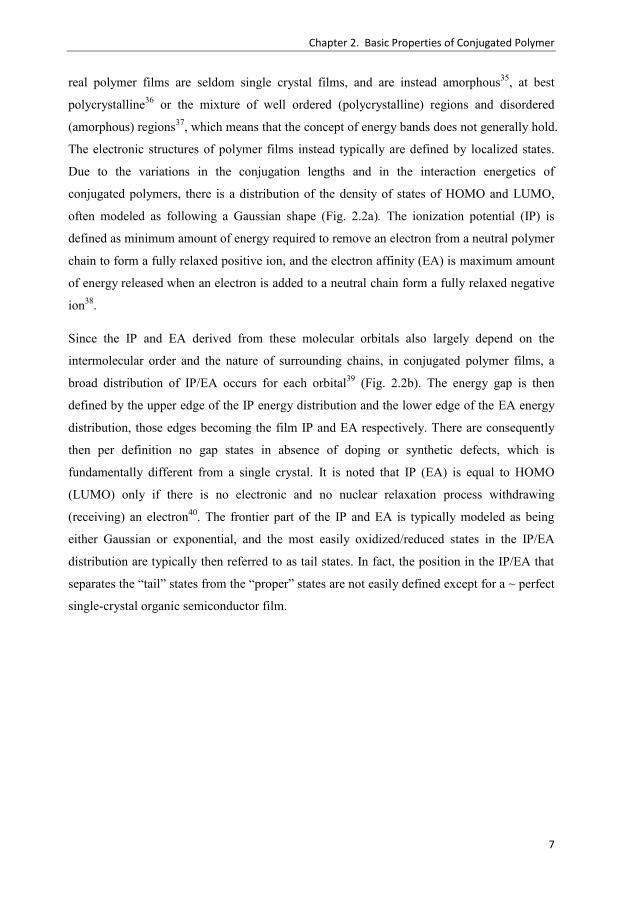
Fig. 2.3 Chemical structures of partial conjugated polymers used in the thesis.
Much attention has been invested into the synthesis of various conjugated polymers with
different electronic structures tailored for their applications in recent years41-44. Fig. 2.3
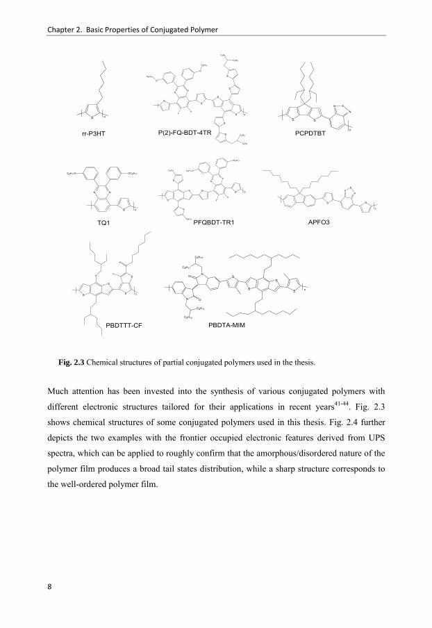
shows chemical structures of some conjugated polymers used in this thesis. Fig. 2.4 further
depicts the two examples with the frontier occupied electronic features derived from UPS
spectra, which can be applied to roughly confirm that the amorphous/disordered nature of the
polymer film produces a broad tail states distribution, while a sharp structure corresponds to
the well-ordered polymer film.
S n
S
F
S
S
SF
S
S
C4H9
C6H9
S
S
C6H9
C4H9
NN
O
C8H17
O
C8H17
n
S S
N
N
S
n
S
N N
OC8H17C8H17O
n
S
S S
FF
S
S
C8H17
S
C8H17
NN
OC8H17
C8H17O
n
S S
NN
S
n
S
S S
SF
O
O
n
rr-P3HT P(2)-FQ-BDT-4TR PCPDTBT
TQ1 PFQBDT-TR1 APFO3
PBDTTT-CF PBDTA-MIM
N O
C6H13
C8H17
NO
C6H13
C8H17
S
S
S
S n
Chapter 2. Basic Properties of Conjugated Polymer
9
Fig. 2.4 Examples of disorder TQ1 and well-order rr-P3HT film with the frontier occupied electronic feature derived from UPS spectra.
2.2 Charge carrier
Unlike inorganic semiconductor, conjugated polymers are soft materials with low charge
carrier mobility and low dielectric constant: adding (withdrawing) an electron to (from)
antibonding LUMO (bonding HOMO), the chain shape and the lattice are deformed to
compensate with significant change in the energy of the now-populated LUMO and
populated HOMO. Therefore, when approaching the energy level alignment for charge
transport and charge injection/extraction barrier, both of previous LUMO and HOMO of the
neutral system are not relevant, and the energy of the singly occupied molecular orbital of the
ionization has to be considered. Depending on backbone of polymer chain, conjugated
polymers have either degenerate or non-degenerate ground state geometry corresponding to
the different nature of charge carriers, e.g. soliton and polaron respectively, which enable
electronic conduction45,46.
The energy of the degenerate ground state is equal for the two configurations due to the
equivalence in order in which the single and double carbon bond arrange alternately, like
2 1 0 -1
(c)
TQ1
disorder
rr-P3HT
tail states
Binding energy (eV)
Inte
nsity
(arb
. uni
ts)
well-order
Chapter 2. Basic Properties of Conjugated Polymer
10
polyacetylene. Soliton gives a localized state in the electronic structure, which locates inside
the HOMO-LUMO gap. The neutral soliton has a spin ½. However, with addition of extra
electron, negatively charged soliton created is spin-less. Extraction of electron leads to the
formation of another spin-less positively charged soliton. Generally, the process is achieved
through doping when charge transfer occurs between the polymer chain and the dopant47.
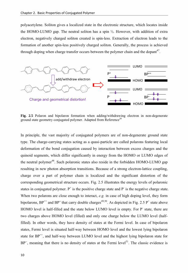
Fig. 2.5 Polaron and bipolaron formation when adding/withdrawing electron in non-degenerate ground state geometry conjugated polymer. Adapted from Reference20
In principle, the vast majority of conjugated polymers are of non-degenerate ground state
type. The charge-carrying states acting as a quasi-particle are called polarons featuring local
deformation of the bond conjugation caused by interaction between excess charges and the
quinoid segments, which differ significantly in energy from the HOMO or LUMO edges of
the neutral polymer48. Such polaronic states also reside in the forbidden HOMO-LUMO gap
resulting in new photon absorption transitions. Because of a strong electron-lattice coupling,
charge over a part of polymer chain is localized and the significant distortion of the
corresponding geometrical structure occurs. Fig. 2.5 illustrates the energy levels of polaronic
states in conjugated polymer. P+ is the positive charge state and P- is the negative charge state.
When two polarons are close enough to interact, e.g. in case of high doping level, they form
bipolarons, BP++ and BP-- that carry double charges49,50. As depicted in Fig. 2.5 P+ state above
HOMO level is half-filled and the state below LUMO level is empty. For P- state, there are
two charges above HOMO level (filled) and only one charge below the LUMO level (half-
filled). In other words, they have density of states at the Fermi level. In case of bipolaron
states, Fermi level is situated half-way between HOMO level and the lowest lying bipolaron
state for BP++, and half-way between LUMO level and the highest lying bipolaron state for
BP--, meaning that there is no density of states at the Fermi level51. The classic evidence is
Charge and geometrical distortion!
add/withdraw electron
LUMO
LUMO
HOMO
HOMO
P+ BP++
P- BP--
Chapter 2. Basic Properties of Conjugated Polymer
11
derived from the UPS measurement on rubidium-doped poly(p-phenylenevinylene) system
reported by Salaneck’s group in 199552. Considering the polaron state within the gap, the
polaron absorption also can be used to identify the presence of polarons in transient
absorption53 and photo-induced absorption measurement54.

12

Chapter 3. Interface Energetics in Organic Electronics
13
Chapter 3. Interface Energetics in Organic Electronics
3.1 Interface categories
Organic electronic devices are made by deposition of successive layers, e.g. organic
semiconductors, metals, oxides or insulators combining in the formation of several interfaces,
and many key electronic processes, e.g. charge injection/extraction, charge recombination
and exciton dissociation, occur at interfaces, which play a critical role in device performance
and function10,11,14-16,19,20,55. It is thus of great importance to understand the energetics at both
organic-metal (electrode) and organic-organic interfaces as well as their influence on the
operational efficiency. When -conjugated polymers are adsorbed on the surface of another
material, the interface energetics may be controlled by several possible effects: interaction
between electron density of polymer and image charge on metal, partial charge transfer
though covalent polymer-metal bonds, integer charge transfer via tunneling across interface
and surface rearrangement as well as absorption-induced orientation, etc14. Depending on the
strength of the interface interaction, the types of conjugated polymer (molecule) interface can
be categorized from strong (chemisorption with covalent bonding) to weak scenario
(physisorption with no charge transfer) as shown in Fig. 3.1.
Fig. 3.1 Category of -conjugated polymer interface. Interface examples: A for OSCs with intrinsic dipole and anchoring groups on clean metal surfaces56; B for OSCs on reactive clean metal surfaces57; C for OSCs on non-reactive clean metal surfaces58; D for OSCs on organic or passivated metal surfaces17; E for noble gas atoms or saturated hydrocarbons on clean metal surfaces59.
A: Strong chemisorption, covalent bonding at specificsites of the molecule and metal, (partial) charge transfer, surface dipole
B: Strong chemisorption, covalent bonding betweenmolecule and metal, (partial) charge transfer,
C: Weak chemisorption, hybridization, possiblepartial charge transfer
D: Physisorption, possible integer charge transfer via tunning
E: Physisorption, no integer charge transfer
Chapter 3. Interface Energetics in Organic Electronics
14
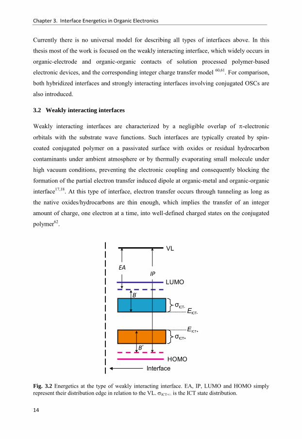
Currently there is no universal model for describing all types of interfaces above. In this
thesis most of the work is focused on the weakly interacting interface, which widely occurs in
organic-electrode and organic-organic contacts of solution processed polymer-based
electronic devices, and the corresponding integer charge transfer model 60,61. For comparison,
both hybridized interfaces and strongly interacting interfaces involving conjugated OSCs are
also introduced.
3.2 Weakly interacting interfaces
Weakly interacting interfaces are characterized by a negligible overlap of -electronic
orbitals with the substrate wave functions. Such interfaces are typically created by spin-
coated conjugated polymer on a passivated surface with oxides or residual hydrocarbon
contaminants under ambient atmosphere or by thermally evaporating small molecule under
high vacuum conditions, preventing the electronic coupling and consequently blocking the
formation of the partial electron transfer induced dipole at organic-metal and organic-organic
interface17,18. At this type of interface, electron transfer occurs through tunneling as long as
the native oxides/hydrocarbons are thin enough, which implies the transfer of an integer
amount of charge, one electron at a time, into well-defined charged states on the conjugated
polymer62.
Fig. 3.2 Energetics at the type of weakly interacting interface. EA, IP, LUMO and HOMO simply represent their distribution edge in relation to the VL. ICT+/- is the ICT state distribution.
InterfaceHOMO
LUMO
σICT-EICT-
EICT+
EA
B-
B+
IP
VL
σICT+
Chapter 3. Interface Energetics in Organic Electronics
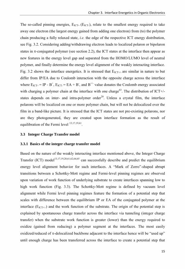
15
The so-called pinning energies, EICT+ (EICT-), relate to the smallest energy required to take
away one electron (the largest energy gained from adding one electron) from (to) the polymer
chain producing a fully relaxed state, i.e. the edge of the respective ICT energy distribution,
see Fig. 3.2. Considering adding/withdrawing electron leads to localized polaron or bipolaron
states in -conjugated polymer (see section 2.2), the ICT states at the interface then appear as
new features in the energy level gap and separated from the HOMO/LUMO level of neutral
polymer, and finally determine the energy level alignment of the weakly interacting interface.
Fig. 3.2 shows the interface energetics. It is stressed that EICT+/- are similar in nature to but
differ from IP/EA due to Coulomb interaction with the opposite charge across the interface
where EICT+ = IP - B+, EICT- = EA + B-, and B+/- value donates the Coulomb energy associated
with charging a polymer chain at the interface with one charge63. The distribution of ICT+/-
states depends on inter- and intra-polymer order20. Unless a crystal film, the interface
polarons will be localized on one or more polymer chain, but will not be delocalized over the
film in a band-like picture. It is stressed that the ICT states are not pre-existing polarons, nor
are they photogenerated, they are created upon interface formation as the result of
equilibration of the Fermi level 13,17,19,61.
3.3 Integer Charge Transfer model
3.3.1 Basics of the integer charge transfer model
Based on the nature of the weakly interacting interface mentioned above, the Integer Charge
Transfer (ICT) model13,17,19,20,61,62,64,65 can successfully describe and predict the equilibrium
energy level alignment behavior for such interfaces. A “Mark of Zorro”-shaped abrupt
transitions between a Schottky-Mott regime and Fermi-level pinning regimes are observed
upon variation of work function of underlying substrate to create interfaces spanning low to
high work function (Fig. 3.3). The Schottky-Mott regime is defined by vacuum level
alignment while Fermi level pinning regimes feature the formation of a potential step that
scales with difference between the equilibrium IP or EA of the conjugated polymer at the
interface (EICT+/-) and the work function of the substrate. The origin of the potential step is
explained by spontaneous charge transfer across the interface via tunneling (integer charge
transfer) when the substrate work function is greater (lower) than the energy required to
oxidize (gained from reducing) a polymer segment at the interfaces. The most easily
oxidized/reduced of -delocalized backbone adjacent to the interface hence will be “used up”
until enough charge has been transferred across the interface to create a potential step that
Chapter 3. Interface Energetics in Organic Electronics
16
equilibrates the Fermi level. The energy where the Fermi level is subsequently pinned is
referred to as EICT+,- (same concept as the smallest energy required to take away one electron
or the largest energy gained from adding one electron at interface producing a fully relaxed
state in session 3.2) depending on if it is positive or negative polarons that are being created.
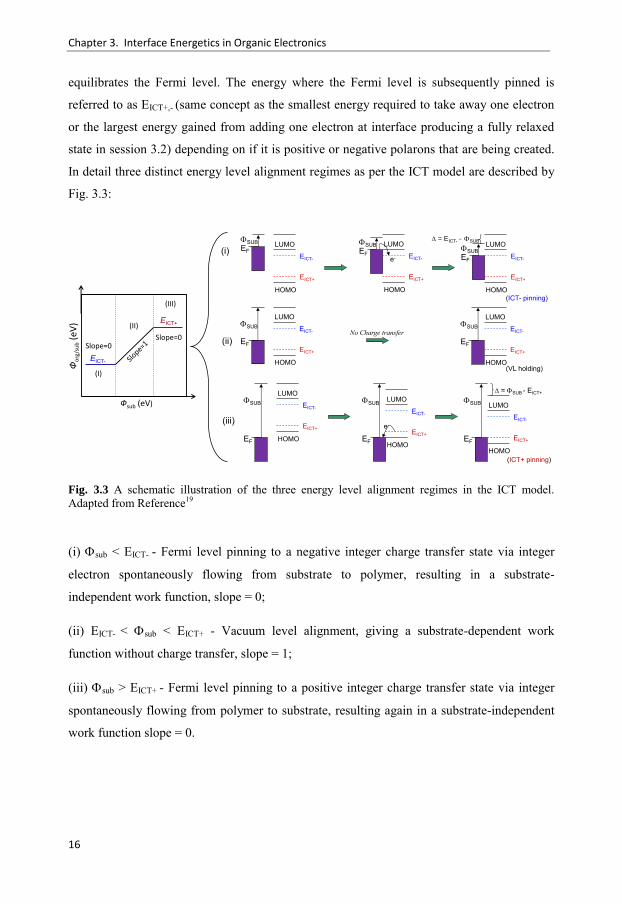
In detail three distinct energy level alignment regimes as per the ICT model are described by
Fig. 3.3:
Fig. 3.3 A schematic illustration of the three energy level alignment regimes in the ICT model. Adapted from Reference19
(i) sub < EICT- - Fermi level pinning to a negative integer charge transfer state via integer
electron spontaneously flowing from substrate to polymer, resulting in a substrate-
independent work function, slope = 0;
(ii) EICT- < sub < EICT+ - Vacuum level alignment, giving a substrate-dependent work
function without charge transfer, slope = 1;
(iii) sub > EICT+ - Fermi level pinning to a positive integer charge transfer state via integer
spontaneously flowing from polymer to substrate, resulting again in a substrate-independent
work function slope = 0.
EICT-
EICT+
(III)
(I)
(II)
Фsub (eV)
Фo
rg/s
ub
(eV
)
(ii)
EF
SUB
HOMO
LUMO
EICT+
EICT-
HOMO
LUMO
EICT+
EICT-
EF
SUB
e-
HOMO
LUMO
EICT+
EICT-
EF
SUB
D = SUB - EICT+
(iii)
(ICT+ pinning)
EF
SUB
HOMO
LUMO
EICT+
EICT-
EF
SUB
HOMO
LUMO
EICT+
EICT-No Charge transfer
(VL holding)
EF
SUB
HOMO
LUMO
EICT+
EICT-
HOMO
LUMO
EICT+
EICT-EF
SUB
e-
HOMO
LUMO
EICT+
EICT-
D = EICT- - SUB
EF
SUB(i)
(ICT- pinning)
Slope=0Slope=0
Chapter 3. Interface Energetics in Organic Electronics
17
Fig. 3.4 ICT behaviors of frequent (a) donor polymers and (b) acceptor fullerenes. D is the energy downshift away from the ideal ICT behavior attributed to the preferential ordering of trisPC60BM adducts. Adapted from Reference23
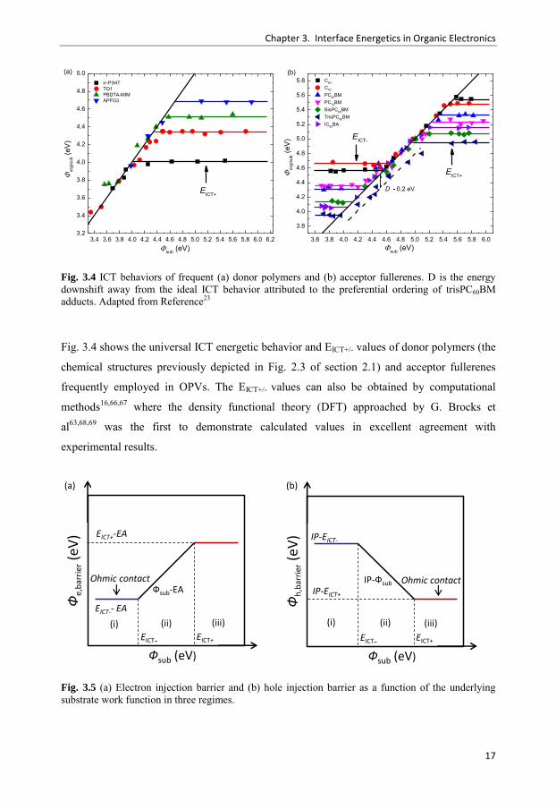
Fig. 3.4 shows the universal ICT energetic behavior and EICT+/- values of donor polymers (the
chemical structures previously depicted in Fig. 2.3 of section 2.1) and acceptor fullerenes
frequently employed in OPVs. The EICT+/- values can also be obtained by computational
methods16,66,67 where the density functional theory (DFT) approached by G. Brocks et
al63,68,69 was the first to demonstrate calculated values in excellent agreement with
experimental results.
Fig. 3.5 (a) Electron injection barrier and (b) hole injection barrier as a function of the underlying substrate work function in three regimes.
3.6 3.8 4.0 4.2 4.4 4.6 4.8 5.0 5.2 5.4 5.6 5.8 6.0
3.8
4.0
4.2
4.4
4.6
4.8
5.0
5.2
5.4
5.6
5.8
3.4 3.6 3.8 4.0 4.2 4.4 4.6 4.8 5.0 5.2 5.4 5.6 5.8 6.0 6.23.2
3.4
3.6
3.8
4.0
4.2
4.4
4.6
4.8
5.0
EICT-
C60
C70
PC60BM PC70BM BisPC60BM TrisPC60BM IC60BA
or
g/su
b (eV
)
sub (eV)
EICT+
D 0.2 eV
(b)
EICT+
org/
sub (
eV)
sub (eV)
rr-P3HT TQ1 PBDTA-MIM APFO3
(a)
Фsub (eV)
Фe,
bar
rier
(eV
)
Ohmic contact
EICT- EICT+
EICT-- EA
EICT+-EA
Фsub (eV)
Фh
,bar
rier
(eV
)
Ohmic contact
EICT- EICT+
IP-EICT+
IP-EICT-
(i) (ii) (iii) (i) (ii) (iii)
(a) (b)
Фsub-EAIP-Фsub
Chapter 3. Interface Energetics in Organic Electronics
18
3.3.2 Organic-electrode interfaces
The ICT model provides a simple and effective path to tailor charge injection/extraction
barrier at electrode interfaces. Energetics at electrode contacts are important as barriers
towards charge injection increase turn-on voltage and decrease the hole-electron
recombination possibility in the case of OLEDs. In the case of OPVs, barriers for charge
extraction diminishes open circuit voltage (Voc) due to the built-in potential reduction,
leading to an increase in carrier recombination and thus a decrease in the short circuit current
(Jsc) as well as the overall power conversion efficiency (PCE). As per the ICT model, the
EICT+/- corresponds to the smallest charge injection barrier in formation of ohmic contact with
adjacent OSC in which the anode work function should be equal or greater than the EICT+ and
the cathode work function equal or smaller than EICT-. In their transition region (ii), the value
of barrier varies as the electrode work function, see Fig. 3.5.
3.3.3 Donor-acceptor interfaces
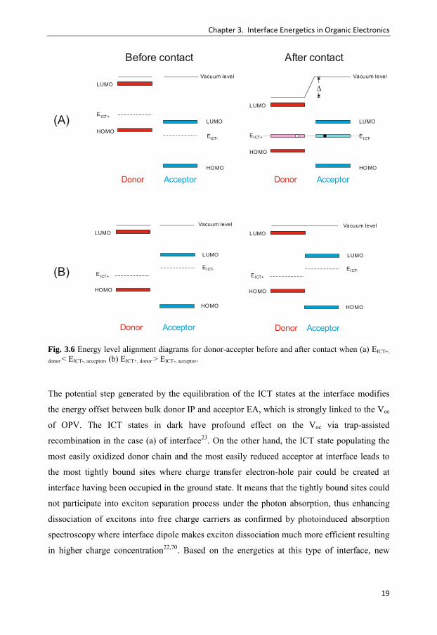
Interface energetics at organic-organic heterojunction can be easily mapped in the ICT model,
which widely exists in OPVs serving as donor-acceptor interface. Fig. 3.6 shows the energy
level alignment process at donor-acceptor interface under the electrode pinned conditions. (a)
When donor EICT+ is smaller than acceptor EICT-, spontaneous electron transfer occurs from
donor to acceptor until the donor ICT+ pinned to acceptor ICT- in formation with a negative
dipole pointing into the acceptor sider. (b) When donor EICT+ is larger than acceptor EICT-, no
charge transfer across the interface and the vacuum level holds.
Chapter 3. Interface Energetics in Organic Electronics
19
Fig. 3.6 Energy level alignment diagrams for donor-accepter before and after contact when (a) EICT+,
donor < EICT-, acceptor, (b) EICT+, donor > EICT-, acceptor.
The potential step generated by the equilibration of the ICT states at the interface modifies
the energy offset between bulk donor IP and acceptor EA, which is strongly linked to the Voc
of OPV. The ICT states in dark have profound effect on the Voc via trap-assisted
recombination in the case (a) of interface23. On the other hand, the ICT state populating the
most easily oxidized donor chain and the most easily reduced acceptor at interface leads to
the most tightly bound sites where charge transfer electron-hole pair could be created at
interface having been occupied in the ground state. It means that the tightly bound sites could
not participate into exciton separation process under the photon absorption, thus enhancing
dissociation of excitons into free charge carriers as confirmed by photoinduced absorption
spectroscopy where interface dipole makes exciton dissociation much more efficient resulting
in higher charge concentration22,70. Based on the energetics at this type of interface, new
HOMO
E ICT+
LUMO
HOMO
EICT-
LUMO
Vacuum level
Donor Acceptor
HOMO
E ICT+
LUMO
HOMO
E ICT-
LUMO
Vacuum level
Donor Acceptor
Before contact After contact
D
HOMO
E ICT+
LUMO
HOMO
E ICT-
LUMO
Vacuum level
Donor Acceptor
HOMO
E ICT+
LUMO
HOMO
E ICT-
LUMO
Vacuum level
Donor Acceptor
(A)
(B)

Chapter 3. Interface Energetics in Organic Electronics
20
design rules for donor-acceptor interface for optimizing open circuit voltage and overall
performance of OPVs were proposed23.
3.4 Hybridized interfaces
Induced Density of Interfacial States (IDIS) model: Here, the interface features hybridization
of the electronic states between -conjugated OSC and the underlying substrate surface,
though no strong covalent bond is formed. In other words, the chemical interaction at
interface is moderate but non-negligible, leading to hybridization of the HOMO and LUMO.
Such interfaces are typically created by vapor deposition of organic molecules onto clean
nonreactive surfaces such as Au and Pt in UHV, and the resulting interaction is slightly
stronger than the weakly interacting interfaces covered by the ICT model mentioned in
section 3.3. The IDIS model58,71-73 is applied to describe such hybridized interfaces. The
model states that there will be a resonance of the molecular states with the metal continuum
of states that then gives rise to a shift and Lorentzian function broadening of both the HOMO
and LUMO introducing a continuous density of states within the band gap, occupied up to the
so-called charge neutrality level (CNL) calculated by integrating the local density of states.
The hybridized interface energetics is determined by the relative position of the organic
molecular CNL and the underlying substrate work function, which is modified by the
interface screening slope parameter S, representing the strength of the interaction. The energy
level alignment is shown in Fig. 3.7. The resulting interface energetics, org/sub and induced
dipole Δ can be expressed as58
Φ𝑜𝑟𝑔/𝑠𝑢𝑏 − CNL = S(Φ𝑠𝑢𝑏 − CNL)
∆= (1 − S)(Φ𝑠𝑢𝑏 − CNL)
S = 𝑑Φ𝑜𝑟𝑔/𝑠𝑢𝑏 𝑑Φ𝑠𝑢𝑏 =⁄ 1 (1 + 4𝜋𝑒2𝐷(𝐸𝐹)𝑑/𝐴)⁄ (3 - 1)
Where D(EF) is the density of states of the interface molecules at the Fermi level, d is the
distance between the molecule and the underlying substrate, and A is the interface area of the
molecule.

Chapter 3. Interface Energetics in Organic Electronics
21
Fig. 3.7 Energy level alignment of organic-metal interface as per IDIS model.
The IDIS model is also used to predict the energy level alignment at organic-organic interface
if the same assumptions of a Lorentzian broadening of molecular orbital energies through
hybridization are adopted. Charge transfer occurs from the high CNL in one side to the low
CNL on the other side of the heterojunction until equilibrium is achieved. In this case, the
slope parameter Soo is used to replace the S at organic-metal interface and the interface dipole
Δoo also depends on Soo and the initial offset of the two CNL levels (Fig. 3.8):72
(CNL1 − CNL2)final = Soo(CNL1 − CNL2)initial
∆oo= (1 − Soo)(CNL1 − CNL2)initial (3 - 2)
Fig. 3.8 Energy level alignment at organic-organic interface as per IDIS model. Adapted from Reference72
Intermolecular hybridization model at donor-acceptor interface: Another model based on
intermolecular hybridization at donor-acceptor interface has recently been proposed by Koch
et al74. The key of the model is that frontier molecular orbital hybridization between the
EF
SUB
HOMO
LUMO
CNL
EF
SUB
D
HOMO
LUMO
CNL
LUMO
HOMO
LUMO
HOMO
CNL1
CNL2
(CNL1-CNL2)final
Δoo
Accptor Donor

Chapter 3. Interface Energetics in Organic Electronics
22
donor HOMO and the acceptor LUMO occurs, leading to the formation of intermolecular
states with a reduced energy gap between a doubly occupied bonding and an unoccupied
antibonding hybrid orbital (Fig. 3.9). This energy level splitting is captured on the
intermolecular resonance integral 𝛽 (or referred to as transfer integral 𝑡 ), and not only
depending on the energy level difference of the individual donor and acceptor, but also on
structure of their molecular orbitals, and, finally, on their relative orientation at interface75.
Fig. 3.9 Intermolecular hybridization at donor-acceptor interface.
The hybridization results in three-component system of donor, acceptor and intermolecular
complex at the donor-acceptor system (Fig. 3.9). The hybridization induced sub-gap
absorption shifts absorption intensity to higher wave lengths, and it is suggested that the
intermolecular orbitals form a barrier to geminate recombination in way similar to a small
insulating tunneling barrier or a cascading energy level in ternary architecture, enhancing the
probability for the charges to escape their mutual Coulomb potential76.
3.5 Strongly interacting interfaces
Strongly interacting interface in which there is a chemical reaction (chemisorption) at
interface often occurring at reactive metal (alkali or alkaline)-organic interface77-79. The
chemical bonding between the metal and organic semiconductor undergoes a net transfer of
charge causing the vacuum level shift introduced by interface dipole, and the up- or down-
shift depends on the electron transfer direction between the two components, which is
Energy
Donor AcceptorIntermolecular
orbitals
HOMO
LUMO
Chapter 3. Interface Energetics in Organic Electronics
23
controlled by their chemical potentials14. Currently, it is hard to model the energetics for this
type of interface, and its energy level alignment is typically obtained experimentally. Perhaps,
one fruitful approach is to view the combination of metal and the chemical reaction layer as
the “new substrate”. Only when the organic molecule contacts with the reactive metal at
interface region, the chemisorption and the strong molecular orbital modification occur, and
the rest of organic molecules in the film far away from the interface are as unperturbed, as
they had been physisorbed on a new created nonreactive substrate. Hence, the ICT model can
be applied to describe the energy level alignment where the new sub is reset. However, the
real interface remains complex since the strength of chemical reaction, the diffusion distance
between metal atom and organic molecule, as well as the intrinsic dipole should be
considered10,14,19.

24

Chapter 4. Photoelectron Spectroscopy and X-ray Absorption Spectroscopy
25
Chapter 4. Photoelectron Spectroscopy and X-ray Absorption
Spectroscopy
The main experiments in this thesis are carried using photoelectron spectroscopy (PES), a
useful tool to probe the energetics at organic-metal and organic-organic interfaces and to
study their bulk and surface chemical states in a single measurement method. PES includes
both traditional X-ray photoelectron spectroscopy (XPS) and ultraviolet photoelectron
spectroscopy (UPS), and it is non-destructive to organic semiconductor materials and
extremely surface sensitive with detection depth of several nanometers. Additionally, another
technique, X-ray absorption often also referred to as near edge absorption fine structure
(NEXAFS) with polarized, monochromatized synchrotron radiation light is useful for the
investigation of molecular orientation (e.g. preferentially edge-on or preferentially plane-on),
which affects the energetics of the organic semiconductor film. All measurements (XPS, UPS
and NEXAFS) are performed in an ultra-high vacuum system with a base pressure of 10-10
mbar to avoid significant electron collision and surface contamination. In this thesis for PES
the energy distribution of the emitted photoelectrons at one fixed excitation energy is
analyzed at the home equipment, for NEXAFS the absorption of X-rays as a function of
photon energy is monitored at beam line D1011 of the MAX-II storage ring at the MAX lab.
4.1 Basics of photoelectron spectroscopy
The principle of PES is based on the photoelectric effect25,80. Light with an energy h
incident on the isolated molecule is absorbed, whereupon an electron of kinetic energy Ek is
emitted from the molecule upon photoionization process following the physical process:
𝑀0 + ℎ𝑣 → 𝑀+∗ + 𝑒− (4 - 1)
M0 represents the isolated neutral molecule in the ground state, M+∗ the positive molecular ion
in the excited state and e- the photoemitted electron. In the same way, their energy relation
can be written as
𝐸0 + ℎ𝑣 = 𝐸+∗ + 𝐸𝑘 (4 - 2)

Chapter 4. Photoelectron Spectroscopy and X-ray Absorption Spectroscopy
26
Where E0 and E+∗ account for the total energy of the neutral molecule and the ionized
molecule, respectively. The photoelectron kinetic energy distribution Ek is measured in order
to deduce the binding energy EBV related to the Vacuum level as follows:
𝐸𝐵𝑉 = 𝐸+
∗ − 𝐸0 = ℎ𝑣 − 𝐸𝑘 (4 - 3)
This equation is used for interpreting PES. EBV thus corresponds to the energy difference
between the initial ground (E0) and various final excited states (E+∗ ). During the photoelectron
emission process, there are electronic relaxation effect occurring. Generally a photoemitted
electron can leave the molecule within 10-15 s. In the process of intramolecular relaxation the
remaining electrons screen the hole in the order of 10-16 s while the nuclear geometric
relaxation time is roughly 10-13 s, which means that the hole is fully screened but the nuclei
are frozen, so that the binding energy shifts to lower values13,51. For molecular solids,
intermolecular relaxation also happens via the electronic polarization of the surrounding
molecule and further helps to screen the hole, causing the additional electron binding energy
shift to lower values as compared to the case of gas phase. The schematic picture of PES
exhibiting photoelectron emission event is shown in Fig. 4.1.
Fig. 4.1 Schematic drawing of PES exhibiting photoemission process including XPS and UPS. The inset indicates the basic working principle of PES. Adapted from Reference51
KINETIC ENERGY MEASURED
BINDING ENERGY
VA
CU
UM
LE
VE
L
INTRAMOLECULAR
ELECTRONIC
RELAXATION
INTERMOLECULAR
ELECTRONIC
RELAXATION
C2
C1
h
e-
C1 C2
CORE
LEVELSVALENCE
LEVELS
UNOCCUPIED
LEVELS
V1,V2,V3
XPS UPSV1
V2 V3
photoelectron
C2-ΔE
ΔE
Chapter 4. Photoelectron Spectroscopy and X-ray Absorption Spectroscopy
27
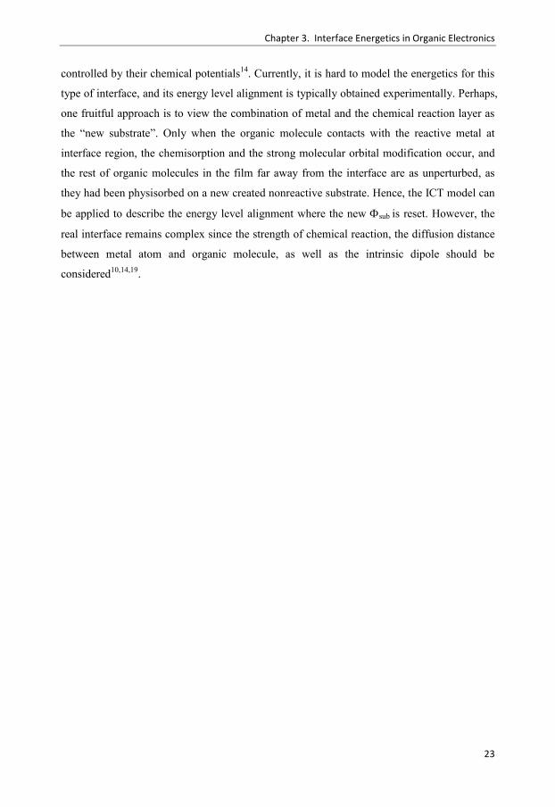
The resulting PES spectra in fact include contributions from all possible final states E+∗
corresponding to the initial ground state, leading to a break down of the one-electron picture.
Fig. 4.2 illustrates the most common final states created upon photoionization. On-set
ionization corresponds to the ionization of electron populating the highest valence level
(UPS), and the process of an ejected electron from a deep core level is referred as the core
level ionization (XPS). The most pronounced PES features originate from the two final states.
In shake up process81, the photoionization includes exciting another electron to the
unoccupied level, leading to decrease in the Ek of the photoemitted electron and the
observation of some low intensity peaks, e.g C2 - ΔE, ( general a less probable process)
accompanying main peak in Fig. 4.1. If the photoionization induces Auger emission, the final
states is different as the molecule becomes doubly ionized82.
Fig. 4.2 Various final states associated with the photoionization.
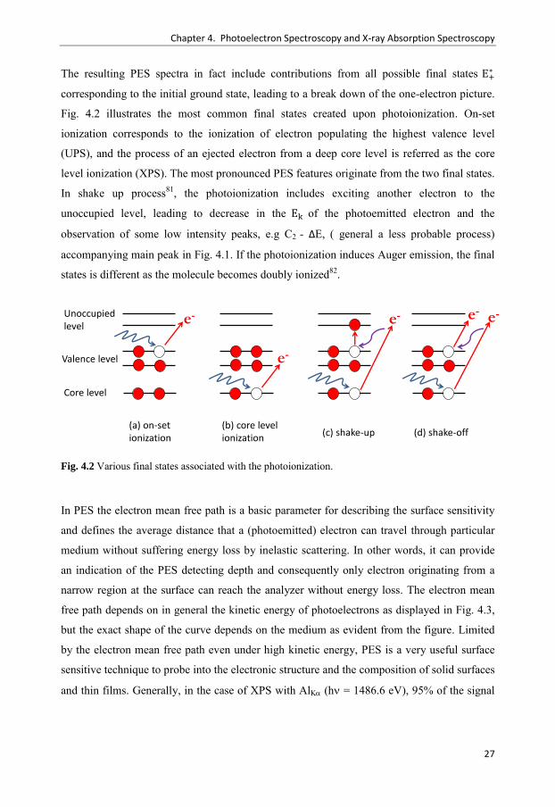
In PES the electron mean free path is a basic parameter for describing the surface sensitivity
and defines the average distance that a (photoemitted) electron can travel through particular
medium without suffering energy loss by inelastic scattering. In other words, it can provide
an indication of the PES detecting depth and consequently only electron originating from a
narrow region at the surface can reach the analyzer without energy loss. The electron mean
free path depends on in general the kinetic energy of photoelectrons as displayed in Fig. 4.3,
but the exact shape of the curve depends on the medium as evident from the figure. Limited
by the electron mean free path even under high kinetic energy, PES is a very useful surface
sensitive technique to probe into the electronic structure and the composition of solid surfaces
and thin films. Generally, in the case of XPS with AlK (h = 1486.6 eV), 95% of the signal
e-
e-
e- e- e-
Core level
Valence level
Unoccupiedlevel
(a) on-set ionization
(b) core levelionization
(c) shake-up (d) shake-off
Chapter 4. Photoelectron Spectroscopy and X-ray Absorption Spectroscopy
28
intensity comes from the top ~100 Å of the film. The detection depth of UPS with HeI (h =
21.22 eV) is even more surface sensitive, about 10 Å.
Fig. 4.3 Inelastic electron mean free path (escape depth) as a function of initial kinetic energy. Figure from Reference83
4.2 Ultraviolet photoelectron spectroscopy (UPS)
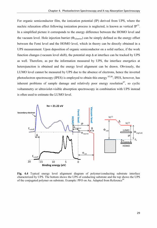
UPS likely is the most important method applied to study the energetics at organic-metal and
organic-organic interfaces. The photon source is typically a helium resonance lamp with HeI
(h = 21.22 eV) or HeII (h = 40.08 eV), and the full width of half maxima (FWHM) is as
narrow as 30 meV84. Such low energy allows a comparatively high cross section for mapping
out not only the valence electronic structures of organic semiconductor but also other
interface parameters like work function Φ , the vertical ionization potential IP and hole
injection barrier (h,barrier) as well as vacuum level shift (Δ) as shown in Fig. 4.4. The work
function Φ is a very important factor determining the minimum energy necessary to remove
an electron from the material. Its value can be derived from the directly measured energy of
the secondary electron cutoff (Ecutoff) where it is the position of zero kinetic energy:
Φ = ℎ𝑣 − 𝐸𝑐𝑢𝑡𝑜𝑓𝑓 (4 - 4)
Chapter 4. Photoelectron Spectroscopy and X-ray Absorption Spectroscopy
29
For organic semiconductor film, the ionization potential (IP) derived from UPS, where the
nucleic relaxation effect following ionization process is neglected, is known as vertical IP13.
In a simplified picture it corresponds to the energy difference between the HOMO level and
the vacuum level. Hole injection barrier (h,barrier) can be simply defined as the energy offset
between the Femi level and the HOMO level, which in theory can be directly obtained in a
UPS measurement. Upon deposition of organic semiconductor on a solid surface, if the work
function changes (vacuum level shift), the potential step Δ at interface can be tracked by UPS
as well. Therefore, as per the information measured by UPS, the interface energetics at
heterojunction is obtained and the energy level alignment can be drawn. Obviously, the
LUMO level cannot be measured by UPS due to the absence of electrons, hence the inverted
photoelectron spectroscopy (IPES) is employed to obtain this energy 85,86; IPES, however, has
inherent problems of sample damage and relatively poor energy resolution87, so cyclic
voltammetry or ultraviolet-visible absorption spectroscopy in combination with UPS instead
is often used to estimate the LUMO level.
Fig. 4.4 Typical energy level alignment diagram of polymer/conducting substrate interface characterized by UPS. The bottom shows the UPS of conducting substrate and the top shows the UPS of the conjugated polymer on substrate. Example: PFO on Au. Adapted from Reference88
h = 21.22 eV
05101520
Ferm
i level
Binding energy (eV)
Secondary electron
Ecutoff
Ecutoff
h,barrier
HO
MO
Δ
Δ
sub
org/sub
Vacu
um
level
IP
VL(1)
VL(2)
HOMO
LUMO
EF
suborg/sub
IP
Δ
h,barrier
Chapter 4. Photoelectron Spectroscopy and X-ray Absorption Spectroscopy
30
4.3 X-ray photoelectron spectroscopy (XPS)
The commonly used X-ray lines of XPS are MgK (h = 1253.6 eV) and monochromated
AlK (h = 1486.6 eV) with FWHM of about 0.8 and 0.4 eV respectively84, which is larger
than that of UPS. The high photon energy gives access to the deep-lying core levels as well as
to the valence region. Because each element has a unique binding energy, the information on
the chemical composition of the surface region can be obtained, and even enables the
possibility of quantitative analysis using atomic sensitivity factor (ASF)89 which also is
limited in its exactness due to inelastic scattering of electrons and cross section effects. The
significant shift in the element core level binding energy is called chemical shift90, which
reflects the chemical environment of the atom such as charge transfer and chemical reaction.
XPS thus proves to be highly useful tool to study possible chemical interactions at an
interface especially for the case of strongly interacting interfaces mentioned in section 3.5. In
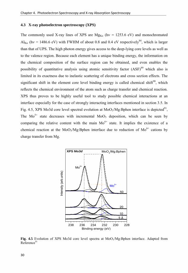
Fig. 4.5, XPS Mo3d core level spectral evolution at MoO3/Mg:Bphen interface is depicted91,
The Mo5+ state decreases with incremental MoO3 deposition, which can be seen by
comparing the relative content with the main Mo6+ state. It implies the existence of a
chemical reaction at the MoO3/Mg:Bphen interface due to reduction of Mo6+ cations by
charge transfer from Mg.
Fig. 4.5 Evolution of XPS Mo3d core level spectra at MoO3/Mg:Bphen interface. Adapted from Reference91
238 236 234 232 230 228
Mo5+
5
Inte
nsity
(arb
.uni
ts)
Binding energy (eV)
XPS Mo3d MoO3/Mg:Bphen
10
20
50
Mo6+
Chapter 4. Photoelectron Spectroscopy and X-ray Absorption Spectroscopy
31
In addition, XPS can also offer the ability to determine the film thickness by monitoring the
attenuation of intensity of the underlying substrate due to organic layer coverage according
to92:
𝐼𝑠 = 𝐼0𝑒−𝑑 𝜆⁄ (4 - 5)
Where Is is the attenuated intensity, I0 is the original intensity, d is the organic film thickness
we want to know and 𝜆 is the electron mean free path in Fig. 4.3.
4.4 X-ray absorption spectroscopy
Near edge X-ray absorption fine structure (NEXAFS) spectroscopy is a powerful tool that
provides information on the unoccupied electronic structure and molecular orientation27,93.
Normally, for low-Z elements (Z is the atomic number) NEXAFS is performed on the K-edge
or L-edge in the binding energy range below 1000 eV93. The excitation of e.g. a K-shell
electron by X-ray source from synchrotron radiation results in either a bound state or a
continuum state. Bound state excitation takes place as either Rydberg transitions or
excitations of 1s electrons to unfilled molecular orbitals labeled as *- or *- orbitals
according to their symmetry. Fig. 4.6 illustrates the corresponding diagram. A 1s → *
transition occurs at energy less than the vacuum level, and a 1s → * transition is found at
higher energy above the vacuum level. It is stressed that a 1s → * transition or * resonance
can only exist for molecules with bonding, such as double and triple bonds. In the Carbon
K-edge NEXAFS spectra of spin-coated rr-P3HT on gold (Fig. 4.7, 90º normal incident), the
peak at 285 eV is related to the transition from C1s to the empty * states. The feature at
around 287 eV is the transition from C1s to the * states of a combination of C-S, C-H and
Rydberg excitations94. The features located at 292 and 302 eV are associated with the 1s →
* of C-C and C=C bonds, respectively. The intensities of these peak shapes correlate
linearly to the stoichiometric bond densities with the measured sampled volume.
I0
Is
d
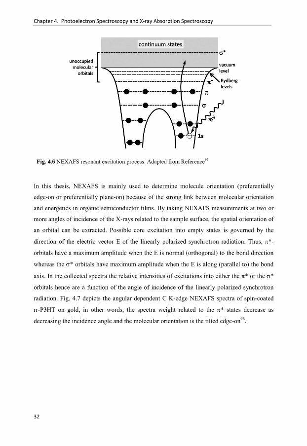
Chapter 4. Photoelectron Spectroscopy and X-ray Absorption Spectroscopy
32
Fig. 4.6 NEXAFS resonant excitation process. Adapted from Reference95
In this thesis, NEXAFS is mainly used to determine molecule orientation (preferentially
edge-on or preferentially plane-on) because of the strong link between molecular orientation
and energetics in organic semiconductor films. By taking NEXAFS measurements at two or
more angles of incidence of the X-rays related to the sample surface, the spatial orientation of
an orbital can be extracted. Possible core excitation into empty states is governed by the
direction of the electric vector E of the linearly polarized synchrotron radiation. Thus, *-
orbitals have a maximum amplitude when the E is normal (orthogonal) to the bond direction
whereas the * orbitals have maximum amplitude when the E is along (parallel to) the bond
axis. In the collected spectra the relative intensities of excitations into either the * or the *
orbitals hence are a function of the angle of incidence of the linearly polarized synchrotron
radiation. Fig. 4.7 depicts the angular dependent C K-edge NEXAFS spectra of spin-coated
rr-P3HT on gold, in other words, the spectra weight related to the * states decrease as
decreasing the incidence angle and the molecular orientation is the tilted edge-on96.
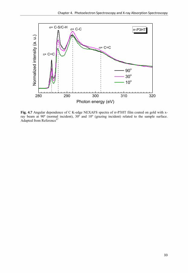
Chapter 4. Photoelectron Spectroscopy and X-ray Absorption Spectroscopy
33
Fig. 4.7 Angular dependence of C K-edge NEXAFS spectra of rr-P3HT film coated on gold with x-ray beam at 90º (normal incident), 30º and 10º (grazing incident) related to the sample surface. Adapted from Reference97
280 290 300 310 320
C=C
C-CC-S/C-H
Nor
mal
ized
inte
nsity
(a. u
.)
90o
30o
10o
rr-P3HT
Photon energy (eV)
C=C

34
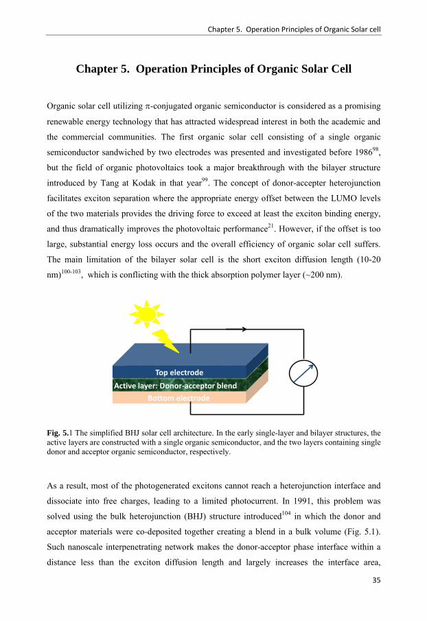
Chapter 5. Operation Principles of Organic Solar cell
35
Chapter 5. Operation Principles of Organic Solar Cell
Organic solar cell utilizing -conjugated organic semiconductor is considered as a promising
renewable energy technology that has attracted widespread interest in both the academic and
the commercial communities. The first organic solar cell consisting of a single organic
semiconductor sandwiched by two electrodes was presented and investigated before 198698,
but the field of organic photovoltaics took a major breakthrough with the bilayer structure
introduced by Tang at Kodak in that year99. The concept of donor-accepter heterojunction
facilitates exciton separation where the appropriate energy offset between the LUMO levels
of the two materials provides the driving force to exceed at least the exciton binding energy,
and thus dramatically improves the photovoltaic performance21. However, if the offset is too
large, substantial energy loss occurs and the overall efficiency of organic solar cell suffers.
The main limitation of the bilayer solar cell is the short exciton diffusion length (10-20
nm)100-103, which is conflicting with the thick absorption polymer layer (~200 nm).
Fig. 5.1 The simplified BHJ solar cell architecture. In the early single-layer and bilayer structures, the active layers are constructed with a single organic semiconductor, and the two layers containing single donor and acceptor organic semiconductor, respectively.
As a result, most of the photogenerated excitons cannot reach a heterojunction interface and
dissociate into free charges, leading to a limited photocurrent. In 1991, this problem was
solved using the bulk heterojunction (BHJ) structure introduced104 in which the donor and
acceptor materials were co-deposited together creating a blend in a bulk volume (Fig. 5.1).
Such nanoscale interpenetrating network makes the donor-acceptor phase interface within a
distance less than the exciton diffusion length and largely increases the interface area,
Bottom electrode
Top electrode
Active layer: Donor-acceptor blend

Chapter 5. Operation Principles of Organic Solar cell
36
consequently, a large fraction of the excitons can be dissociated into free charges and the
device efficiency is significantly improved. Currently, the BHJ structure is dominant and
widely used in fabricating organic solar cell device with the rapidly rising energy conversion
efficiency of up to 11% for single-junction cell8,9. Moreover, the ternary BHJ structure
composed of two donors and one acceptor also starts to be studied in order to enhance the
light absorption and suppress charge recombination by creating the cascade energy levels105.
Depending on the deposition order of anode and cathode in organic solar cell, conventional
BHJ solar cell features a bottom indium tin oxide (ITO) modified by PEDOT:PSS with high
work function as anode and a top low work function metal as cathode, contrarily, inverted
device features a low work function interlayer, e.g. transition metal oxide (ZnOx), conjugated
polymer (PFN), or insulator (PEIE) coated on ITO that acts as the bottom cathode and an air-
stable high work function metal or metal oxide, e.g. Au and MoOx as the top anode106,107.
The latter case on the one hand raises the operation lifetime, on the other hand, matches well
with the vertical phase separation of BHJ layer and thus enhances charge collection at the
organic-electrode interface.
Fig. 5.2 Schematic illustration of the fundamental process of BHJ solar cell.
During the operation of organic solar cell, the fundamental conversion process from light into
electricity in a BHJ solar cell can be schematically described by steps of (Fig. 5.2): (a)
+
-
+
-
--
-a b
c
de
f
Anode Cathode
Donor Acceptor
Chapter 5. Operation Principles of Organic Solar cell
37
exciton creation through light absorption in the active layer, (b) exciton diffusion to the
donor-acceptor interface, (c) exciton dissociation and charge-transfer (CT) exciton formation
bound by Coulomb force, (d) CT exciton dissociation into free charge carrier, (e) charge
carrier transport towards electrodes, (f) charge carrier collection at electrode interface,
producing photocurrent.
Light absorption is controlled by the band gap of the active layer. In order to enhance the
number of absorbed photons, the band gap of organic semiconductor should be narrow to
capture as much as possible of the solar spectrum. However, the smaller band gap causes
much energy loss due to the thermalization process when the higher energy photons are
absorbed. Therefore, a trade-off exists between the quantity of the photons absorbed and the
absorbed photon energy, pointing to an optimized band gap of 1.1-1.3 eV as suggested by the
Shockley-Queisser limit108. In addition, the tandem structure with several complementary
components is also applied to broaden the total absorption spectrum109. The created excitons
are strongly bound with a binding energy of up to 0.5 eV110 and thermally diffuse to the
donor-acceptor interface within a distance less than the excition diffusion length (10-20 nm)
within their lifetime. As noted, if the excitons cannot reach the interfaces, they will instead
recombine.
At the donor-acceptor interface, electrons might transfer from the donor excitons to the
electronegative acceptor, driven by an energy offset (normally referred as 0.3 eV)21 between
the donor and acceptor LUMO so as to overcome the initial Coulomb binding energy of the
excitons. As donor and acceptor molecule phases are physically adjacent to each other at the
interface, the dissociated electron-hole pairs are still bound with a significant Coulomb
attraction forming so-called charge-transfer (CT) states. It is reported that the binding energy
of the CT state is estimated in the range 0.1-0.5 eV111-113, which is larger than the thermal
energy (~0.025 eV) at room temperature and thus indicates an energetic barrier that exists for
CT exciton dissociation into free charge carrier. The CT exciton separation plays a crucial
role in function of the organic solar cell, affecting not only the short circuit current but also
open circuit voltage114,115. Fig. 5.3 summarizes the photocurrent process involved in CT
exciton generation, separation and recombination. The inefficient CT excitons lead to
germinate recombination to form either the ground state (KGR) or the triplet exciton (Ktriplet).
At the stage of CT state separation, the two kinetic competitions occur. One is between
thermalization and dissociation of the hot CT states, that is to say that the hot CT states
directly dissociate into charge-separated (CS) states (Kcs*) contributing to charge

Chapter 5. Operation Principles of Organic Solar cell
38
photogeneration, but the hot CT state can thermally relax to the lowest excited state (KthermCT ).
Another competition is between the geminate recombination (KGR or Ktriplet) and dissociation
of the relaxed CT state (Kcs0) into CS states. The separation distance of electron-hole pairs
continuously increases and thus the excitons suffer less Coulombic attraction, finally, the free
charge carriers are created beyond the Coulomb force.
Fig. 5.3 Energy level diagram for CT exciton generation, separation and recombination. Adapted from Reference112
During the process of the free charge carrier transport towards electrode for photocurrent
generation, several recombination steps generally including bimolecular recombination (KBR),
trap-assisted recombination and surface recombination occur that decrease the photocurrent
and the overall power efficiency of the device. The former follows the Langevin expression
and the rate depends on the probability of free holes and electrons meeting each other116. The
middle is known as the Schockley-Read-Hall recombination23. The trap states are mainly
caused by impurities and defects in active layer as well as interfacial states resulted from
oxidation/reduction polymer segment. The latter happens on the electrode surface and can be
suppressed through surface state cut-down, e.g. passivation treatment and inserting ideal
interlayer106,117.
-
+
S1
T1
S0
KCT
Ktriplet
KGR
CT* (hot)
CT0
KthermCT
KCS*
KCS0
CS*
KBR
CS0
KthermCS
hvEne
rgy
(eV
)

Chapter 6. Summary of Papers Included in the Thesis
39
Chapter 6. Summary of Papers Included in the Thesis
Six publications included in this thesis have given the deeper understanding of interface
phenomena regarding both donor-acceptor and active layer-electrode interfaces in BHJ OPVs,
which are combined with the ICT model applied both to interface energetics of organic
semiconductor and to the design of OPVs in order to improve the efficiency and lifetime.
Paper I proposes new design rules for donor-acceptor interface to optimize open circuit
voltage and overall performance of OPVs, in fact enabling not just efficient screening of
OSC donor and acceptor materials but also in silico design thereof. Paper II presents
research on the two different degradation mechanisms of interface energetics of PCBM-
electrode interface caused by oxygen and water, respectively. Paper III proposes a general
model for energy level bending in absence of significant doping of conjugated polymer film,
showing experimental results that overturn some of the recent models. Papers IV and V are
devoted to the development of a universal model for handling energetics that simultaneously
treats doped conjugated polymer and conjugated electrolyte/electrode interface, which are
two established methods for improving charge injection/exaction efficiency. Paper VI
addresses the effect of processing (and the environment), i.e. UV-light soaking under
different conditions, on surface electronic structures of the interlayer ZnO nanoparticle film
and the OPV performance.
Chapter 6. Summary of Papers Included in the Thesis
40
6.1 Paper I
Trap-Assisted Recombination via Integer Charge Transfer States in Organic Bulk
Heterojunction Photovoltaics
Q. Y. Bao, O. Sandberg, D. Dagnelund, S. Sanden, S. Braun, H. Aarnio, X. J. Liu, W. M.
Chen, R. Österbacka, and M. Fahlman
Advanced Functional Materials, 2014, 24, 6309
Charge transfer (CT) complexes play an important influence on the efficiency of bulk
heterojunction solar cells. These studies have always focused on the photogenerated CT
complexes but the presence and effect of integer charge transfer (ICT) states presented in the
dark and created as a consequence of Fermi level equilibrium has all but been ignored so far,
despite indications of their significance.
In the Paper I, we use a series of regioregular-poly(3-hexylthiophene):fullerene (C60/70,
PC60/70BM, BisPC60BM, TriPC60BM and IC60BA) bulk heterojunction solar cells with pinned
electrodes to show ICT states are often formed at the bulk heterojunction interface and have a
profound effect on the open circuit voltage (Voc). Normally, the donor ionization potential to
acceptor electron affinity energy difference is thought to be an upper limit of the device Voc,
but the effective energy gap should include possible potential steps at the bulk heterojunction
that is the relevant parameter. The experiments reveal that the ICT state formation causes
vacuum level misalignment that yields a roughly constant effective donor ionization potential
to acceptor electron affinity energy difference at the series of rr-P3HT:fullerene interfaces,
even though there is a large variation in the fullerene series’ electron affinity. This is a radical
departure from common wisdom, which e.g. holds that the improved Voc using IC60BA as
compared to PC60BM in combination with rr-P3HT is due to a better matching between the
energy levels of rr-P3HT and those of the fullerene. We highlight that the large variation in
Voc for the device series featuring different fullerenes instead is found to be a consequence of
variations in trap-assisted recombination via ICT states, and we demonstrate this holds true if
one assumes a pn junction or metal-insulator-metal based description of bulk heterojunction
solar cells. Electron paramagnetic resonance measurements confirm the creation of ICT states
at the bulk heterojunctions in the dark and together with photo-assisted absorption
measurements show that the donor/acceptor coupling strength and recombination-induced
loss can be predicted as per the ICT model. The results enable us to propose novel design

Chapter 6. Summary of Papers Included in the Thesis
41
rules for the donor/acceptor materials using measured or DFT calculated ICT states for bulk
heterojunction solar cells:
(i) Pinned electrode contacts are obtained by: anode ≥ EICT+,D and cathode ≤ EICT-,A
(ii) Donor:acceptor combinations should be chosen so that EICT-,A ≈ EICT+,D
The design rules are tested against a set of high performing donor polymers and their
corresponding fullerene-based OPV devices available in literature, and excellent correlation
is obtained. See Fig.6.1.
Fig. 6.1 Experimental Voc loss plotted against the EICT+,D (Donor) - EICT-,A (Acceptor) for a set of polymer:fullerene bulk heterojunction solar cells.
-0.6 -0.4 -0.2 0.0 0.2 0.4
0.2
0.4
0.6
0.8
1.0
EIC
T-, A
EIC
T+,D
EICT-, A EICT+,D
PFQBDT-TR:PC60BM PCPDTBT:PC60BM rr-P3HT:TrisPC60BM PBDTTT-CF:PC70BM PBDTA-MIM:PC60BM APFO-Green1:PC60BM APFO3:PC60BM
rr-P3HT:C70 rr-P3HT:C60 rr-P3HT:PC70BM rr-P3HT:PC60BM rr-P3HT:BisPC60BM rr-P3HT:IC60BA P(2)-FQ-BDT-4TR:PC60BM TQ1:PC70BM
Voc
loss
(V)
EICT+,D- EICT-,A (eV)
EICT-, A EICT+,D
Chapter 6. Summary of Papers Included in the Thesis
42
6.2 Paper II
Oxygen- and Water-Based Degradation in [6, 6]-Phenyl-C61-Butyric Acid Methyl Ester
(PCBM) Films
Q. Y. Bao, X. J. Liu, S. Braun, and M. Fahlman
Advanced Energy Materials, 2014, 4, 1301272
The understanding of degradation mechanism and stability of PCBM film as a common
component in OPVs when exposed to atmosphere is expected to aid in further development
of both organic semiconductor materials and in device engineering.
In the Paper II, we probe into the effects of in situ oxygen and water vapor separately on the
energetics of PCBM films in UHV. The modification of PES features originates from
interaction between the fullerene part of PCBM and oxygen or water molecules. The results
show that the degradation mechanisms of PCBM film induced by oxygen and water are
absolutely different. Upon exposure to oxygen gas, the work function downshifts by ~ 0.15
eV both for pinned (EICT+/-) and vacuum level aligned interfaces compared to the ICT curve
of pristine PCBM film, which is incompatible with oxidation/p-doping. We speculate it
results from energy level bending due to defect states located above the EICT- level of PCBM,
and the other possible explanation is the double dipole model proposed in Paper IV as the
negatively charged oxygen species are more mobile than the hole-carrying PCBM. The IP
value and UPS spectra features of the PCBM film are not affected and the oxygen
degradation effect is reversible by thermal treatment in UHV, indicating a weak interaction
between oxygen and PCBM molecules. When exposed to water, water vapor induces the
occupied valence structure to undergo irreversible and strong modification (extensive
broadening and blending of the frontier features in the UPS spectra) accompanied by the
significant change of O1s and C1s XPS core spectra. The work function and IP decrease
without a saturation trend within the studied exposure times. This suggests that significant
chemical reaction occurs between the water and PCBM. According to these findings, in the
case of oxygen induced degradation, a downward energy level bending in PCBM domains at
the extracting contact would cause Voc loss, whereas it would aid positively free charge
generation by sweeping away electrons from the D-A interface. The strong irreversible
degradation of the electronic structure from water exposure is likely to negatively affect the
transport properties of the PCBM.
Chapter 6. Summary of Papers Included in the Thesis
43
6.3 Paper III
The Energetics of the Semiconducting Polymer-Electrode Interface for Solution-
Processed Electronics
Q. Y. Bao, S. Fabiano, M. Andersson, S. Braun, Z. Y. Sun, X. Crispin, M. Berggren, X. J.
Liu, and M. Fahlman
(Submitted)
The spatial dependence of energy levels in organic semiconductor film induced by charge
transfer across a heterojunction strongly influences charge injection and transport as well as
exciton dissociation in organic electronic devices. The current views about energy level
bending (ELB) in conjugated polymer films, e.g. experimental observations and models, are
largely divergent, which are derived from films fabricated by spin-coating that can easily
yield partial coverage/pin hole in the ultrathin film.
In the Paper III, we use the original approach of building and characterizing multilayers
composed of a well-defined number of polymer monolayers with the Langmuir-Shäfer
method. This allows us to track spatial dependence of ELB at a precision never achieved for
semiconducting polymers, avoiding artefacts from spin-coating. The evolutions for both work
function and the occupied electronic structures are probed by PES in ultrahigh vacuum and
the order in the films is detected by a combination of AFM, NEXAFS and PL techniques.
The TQ1 disorder film features smaller, and in fact negligible, ELB compared to the rr-P3HT
more well-ordered film, in other words, an increase in local disorder yields a narrower ELB,
in contradiction with existing models (Fig. 6.2a). We propose a general model for energy
level bending in absence of significant doping of conjugated polymer film (Fig. 6.2c). The
study highlights that ELB depends on the distribution of oxidation/reduction energies in the
polymer layer compared with the position of the Fermi level, taking into account the
Coulomb energy associated with charging the polymer chain and transferring a charge across
the interface (Fig. 6.2b). The consequence of this is that almost all the potential shift
necessary to equilibrate the Fermi level occurs over the first 1-2 monolayers at an interface
(Fig. 6.2c). An extended ELB region featuring a significant potential shift away from the
interface may still occur for well-ordered films with delocalized polarons or if there is a
strong order-dependence of the organic semiconductor EICT+,-. Under such scenarios more

Chapter 6. Summary of Papers Included in the Thesis
44
extended ELB regions in organic semiconductor films can occur even in absence of
significant doping-induced free charge density.
Fig. 6.2 ELB formation mechanism in conjugated polymer film. (a) Model (i) assumes that there is no Coulomb energy associated with charging the polymer chain and transferring a charge across the interface. (b) Coulomb interaction between charges in the polymer layer at interface and the mirror charges across interface. (c) Model (ii) assumes that there is energy related to charging the polymer film including Coulomb interaction between the electron transferred to the substrate and the hole left on the OSC molecule/polymer. Charge transfer occurs when part of the integer charge transfer energy distribution is above the Fermi level.
Vacuum level
OSC ICT+distribution
DOS
Ener
gy
EF
ФSUB
ELB
Monolayer
Vacuum level
OSC HOMOdistribution
DOS
Ener
gy
EF
ФSUB
ELB
Monolayer
Model (i)
Model (ii)
+
+
+
+
–
–
substrate polymer layer
1st 2nd
(b)
(a)
(c)

Chapter 6. Summary of Papers Included in the Thesis
45
6.4 Paper IV
Energetics at Doped Conjugated Polymer/Electrode Interfaces
Q. Y. Bao, X. J. Liu, S. Braun, F. Gao, and M. Fahlman
Advanced Materials Interfaces, 2015, 2, 1400403
Doping has been proved to be a powerful technique able to improve the efficiency of organic
electronics by tuning the electronic properties of organic semiconductor. Unlike the case of
the pristine organic semiconductor that follows the ICT model, a universal model for energy
alignment at molecule-doped conjugated polymer/electrode interface is still not established.
In the Paper IV, the energetics at molecule F4TCNQ doped polycrystalline rr-P3HT and
amorphous TQ1 polymer, respectively, with various doping concentrations/conducting
substrates interfaces are investigated. Regular plots with a constant thickness-independent
displacement away from the original energy level alignment behavior of the pristine polymer
at low to intermediate level for molecule-doped conjugated polymer interfaces are observed,
and that at high doping level are substrate-independent. We propose an universal model for
describing this class of interfaces: (i) equilibration of the Fermi level due to oxidation (or
reduction) of polymer sites at the interface as described by ICT model and additionally (ii) a
double dipole step induced by image charge from the dopant-polymer charge transfer
complex that cause a shift of the work function for both pinned (S = 0) and unpinned (S = 1)
interfaces. Such behavior is expected to hold for all low to intermediate level doped polymer
systems. For high doping levels (significant density of free charges at the interface), the
classic depletion layer model is found to hold.
Chapter 6. Summary of Papers Included in the Thesis
46
6.5 Paper V
Regular Energetics at Conjugated Electrolyte/Electrode Modifier for Organic
Electronics and Their Implications of Design Rules
Q. Y. Bao, X. J. Liu, E. G. Wang, J. F. Fang, F. Gao, S. Braun, and M. Fahlman
(Submitted)
Conjugated electrolytes (CEs) are very efficient charge injection/extraction interlayers for
device operation due to their ability to effectively modify the work function of bare
electrodes. CEs feature both -conjugated electronic structures and ions, therefore, it is
reasonable to expect that CE/electrode energetics can be described by combination of the ICT
model and models based on non-conjugated electrolytes.
In the Paper V, through systematically studying a CE series with various ionic groups
including cationic PFN, TQm8-N, PFNBr, anionic P3CBT and zwitterionic P(NSO3)2, a
general model for energy level alignment at CE/electrode interfaces is presented: (i)
equilibration of the Fermi level due to oxidation/reduction of -delocalized backbone at
interface as per the ICT model in combination with (ii) an additional interface dipole step
induced by ion migration or side chain electrostatic realignment, which is similar to the
results in Paper IV. These models reveal how to manipulate the energetics of CE/electrode
interfaces to achieve the smallest charge injection/extraction barriers and bypass the current
interlayer thickness limitation: (a) Acceptor (n-type) cationic CEs should be near ideal for
designing electron injecting CE/electrode contacts, as the acceptor nature of these materials
enable pinning to the ICT- states even for moderately high work function electrodes (< 4.6
eV or so). Pinning in the (i) region of the ICT curve ensures the lowest Φe,barrier and hence
efficient electron injection and transport even for thicker CE layers. Anionic CEs should have
donor (p-type) -delocalized backbones, enabling pinning in the (iii) region under the
moderate Φel and the lowest Φh,barrier at the CE/electrode interface regardless of thickness.

Chapter 6. Summary of Papers Included in the Thesis
47
6.6 Paper VI
Effects of Ultraviolet Soaking on Surface Electronic Structures of Solution Processed
ZnO Nanoparticle Films in Polymer Solar Cells
Q. Y. Bao, X. J. Liu, Y. X. Xia, F. Gao, L. D. Kauffmann, O. Margeat, J. Ackermann, and M.
Fahlman
Journal of Materials Chemistry A, 2014, 2, 17676
The photovoltaic performance has been demonstrated to be sensitive to surface electronic
structure of cathode interlayer. ZnO nanoparticle (ZnONP) film provides well matching
contact energetics with the active layer for tuning cathode side.
In the Paper VI, we explore the effect of UV-light soaking on surface electronic structures
and chemical states of solution processed ZnONP film in UHV, dry air and UV-ozone. We
find that its surface properties are very sensitive to the UV irradiation. UV soaking in UHV
induces a slight decrease in both work function and oxygen-deficient component, and an
almost negligible downshift in valence band. For UV-light soaking in presence of oxygen, the
work function increases accompanied by a smaller energy offset between the valence band
edge and Fermi level. A decrease of the oxygen-defect component and a slight increase of the
ZnO matrix feature are observed that is attributed to the desorption of oxygen molecules from
the surface and filling of oxygen atoms in the ZnO matrix. The work function of ZnONP film
can be tuned over a range spanning more than 1 eV using this technique. Deriving from
photovoltaic and diode measurements, it is concluded that the high work function ZnONP
films retains their n-type behavior as the oxygen vacancy filling from the UV-ozone soaking
seems concentrated to the surface of the films. Enhancement in short current density can be
obtained as filling of surface vacancies reduce carrier recombination at fullerene/ZnONP
interface.

48
Chapter 7. Future Outlook
49
Chapter 7. Future Outlook
Photoelectron spectroscopy: PES-derived IP measurement does not take geometrical
relaxation contribution to the polaron energy into account and thus is not accurately equated
with the charge injection/extraction barrier. In addition, different types of organic electronics
utilize different part of the polaron density of states, generally sending to lower carrier
concentrations from OTFTs, OLEDs, OPVs to organic spin valves. The relevant part of
density of states may be far into the tail states or even is covered up by the normal PES
background. Therefore, further achieving the accurate energetics of polaron density states,
detecting the tail states with the ultrahigh-sensitivity UPS or modeling, and investigating the
effect of tail states on the OPV efficiency that is in fact ignored so far, are of tremendous
importance.
Donor-acceptor interface design: A new design rule for donor-acceptor interface based on
polymer:fullerene BHJ OPVs to optimize open circuit voltage has been proposed and tested
in this thesis. An examination of extending this rule into small molecule blends is in process.
As per the rule, tailoring the energy of negative integer charge transfer states of common
fullerenes to match with that of high efficiency donor materials is one interesting topic.
Hybridization effect at donor-acceptor interface: Recently OSC doping microscopic
mechanisms are controversial between integer charge transfer and hybridization. It means
that the latter model makes the frontier orbital hybridization between the donor HOMO and
the acceptor LUMO, leading to a strong ground state bleach attributed to the formation of
charge-transfer complexes with a reduced energy gap that would capture higher light wave
lengths, and create the cascading energy levels enhancing the exciton dissociation. Donor-
acceptor interface in OPVs following the ICT model has been generally accepted, but
hybridization still can occur when the parameters, e.g. the individual energy levels of donor
and acceptor materials, the special structure of their frontier orbitals and their relative
orientation at interface, are satisfied. This design approach for donor-acceptor interface may
have a potential in OPV application.
Selection principle of electrode modifier: Many soft materials have been widely used to
tailoring electrode for improving charge injection/extraction efficiency and operation lifetime,
and a universal model for energetics of conjugated electrolyte-electrode interface was

Chapter 7. Future Outlook
50
proposed in this thesis. However, the modified work function may originate from push back
effect, charge transfer dipole and intrinsic dipole as well as other possible contribution.
Unlocking the relation between the chemical structure of material and its interface energetics,
finally understanding the selection principle of “green” electrode modifier is necessary.

References
51
References
1 Zaumseil, J. & Sirringhaus, H. Electron and ambipolar transport in organic field-effect transistors. Chem. Rev. 107, 1296-1323 (2007).
2 Tang, C. W. & Vanslyke, S. A. Organic lectroluminescent diodes. Appl. Phys. Lett. 51, 913-915 (1987).
3 Yu, G., Gao, J., Hummelen, J. C., Wudl, F. & Heeger, A. J. Polymer photovoltaic cells - enhanced efficiencies via a network of internal donor-acceptor heterojunctions. Science 270, 1789-1791 (1995).
4 Zimmerman, J. D. et al. Porphyrin-tape/C60 organic photodetectors with 6.5% external quantum efficiency in the near infrared. Adv. Mater. 22, 2780-2783 (2010).
5 Scott, J. C. & Bozano, L. D. Nonvolatile memory elements based on organic materials. Adv. Mater. 19, 1452-1463 (2007).
6 Riechel, S. et al. Very compact tunable solid-state laser utilizing a thin-film organic semiconductor. Opt. Lett. 26, 593-595 (2001).
7 Dediu, V. A., Hueso, L. E., Bergenti, I. & Taliani, C. Spin routes in organic semiconductors. Nat. Mater. 8, 707-716 (2009).
8 www.m-kagaku.co.jp. 9 www.heliatek.com. 10 Hwang, J., Wan, A. & Kahn, A. Energetics of metal-organic interfaces: New experiments
and assessment of the field. Mat. Sci. Eng. R. 64, 1-31 (2009). 11 Shoaee, S. et al. Charge photogeneration in donor/acceptor organic solar cells. J. Photon
Energy 2, 021001 (2012). 12 Maurano, A. et al. Recombination dynamics as a key determinant of open circuit voltage in
organic bulk heterojunction solar cells: a comparison of four different donor polymers. Adv. Mater. 22, 4987 (2010).
13 Fahlman, M. et al. Photoelectron spectroscopy and modeling of interface properties related to organic photovoltaic cells. J. Electron Spectrosc. Relat. Phenom. 190, 33-41 (2013).
14 Ishii, H., Sugiyama, K., Ito, E. & Seki, K. Energy level alignment and interfacial electronic structures at organic/metal and organic/organic interfaces (vol 11, pg 605, 1999). Adv. Mater. 11, 972-972 (1999).
15 Koch, N. Organic electronic devices and their functional interfaces. Chemphyschem 8, 1438-1455 (2007).
16 Greiner, M. T. et al. Universal energy-level alignment of molecules on metal oxides. Nat. Mater. 11, 76–81 (2012).
17 Tengstedt, C. et al. Fermi-level pinning at conjugated polymer interfaces. Appl. Phys. Lett. 88, 053502 (2006).
18 Crispin, A., Crispin, X., Fahlman, M., Berggren, M. & Salaneck, W. R. Transition between energy level alignment regimes at a low band gap polymer-electrode interfaces. Appl. Phys. Lett. 89, 213503 (2006).
19 Braun, S., Salaneck, W. R. & Fahlman, M. Energy-level alignment at organic/metal and organic/organic interfaces. Adv. Mater. 21, 1450-1472 (2009).
20 Fahlman, M. et al. Electronic structure of hybrid interfaces for polymer-based electronics. J. Phys-Condens. Mat. 19, 183202 (2007).
21 Scharber, M. C. et al. Design rules for donors in bulk-heterojunction solar cells - Towards 10 % energy-conversion efficiency. Adv. Mater. 18, 789 (2006).
22 Aarnio, H. et al. Spontaneous charge transfer and dipole formation at the interface between P3HT and PCBM. Adv. Energy Mater. 1, 792-797 (2011).

References
52
23 Bao, Q. Y. et al. Trap-assisted recombination via integer charge transfer states in organic bulk heterojunction photovoltaics. Adv. Funct. Mater. 24, 6309-6316 (2014).
24 Bai, S. et al. Ethanedithiol treatment of solution-processed ZnO thin films: controlling the intragap states of electron transporting interlayers for efficient and stable inverted organic photovoltaics. Adv. Energy Mater. DOI: 10.1002/aenm.201401606.
25 Salaneck, W. R., Strafström, S. & Bredas, J. L. Conjugated polymer surfaces ansd interfaces: electronic and chemical structure of interfaces for polymer light emitting devices. Cambridge University Press, Cambridge, 1996.
26 Koch, N., Ueno, N. & Wee, S. T. W. The Molecule-Metal Interface. Wiley, 2013. 27 Hahner, G. Near edge X-ray absorption fine structure spectroscopy as a tool to probe
electronic and structural properties of thin organic films and liquids. Chem. Soc. Rev. 35, 1244-1255 (2006).
28 Chiang, C. K. et al. Electrical-conductivity in doped polyacetylene. Phys. Rev. Lett. 39, 1098-1101 (1977).
29 Pope, M. & Swenberg, C. E. Electronic Processes in Organic Crystals and Polymers. Oxford University Press, Oxford, 1999.
30 Smits, E. C. P. et al. Bottom-up organic integrated circuits. Nature 455, 956-959 (2008). 31 Feng, G. Loss Mechanisms in Bulk Heterojunction Organic Photovoltaics. University of
Cambridge ,Ph.D thesis (2011). 32 Moliton, A. & Hiorns, R. C. Review of electronic and optical properties of semiconductingπ-
conjugated polymers: applications in optoelectronics. Polymer International 53, 1397-1412 (2004).
33 Fahlman, M. & Salaneck, W. R. Surfaces and interfaces in polymer-based electronics. Surf. Sci. 500, 904-922 (2002).
34 Marsh, R. A. Charge recombination and separation in excitonic photovolatics cells. University of Cambridge ,Ph.D thesis (2009).
35 Chen, X. L. et al. Ion-modulated ambipolar electrical conduction in thin-film transistors based on amorphous conjugated polymers. Appl. Phys. Lett. 78, 228-230 (2001).
36 Street, R. A., Northrup, J. E. & Salleo, A. Transport in polycrystalline polymer thin-film transistors. Phys. Rev. B 71, 165202 (2005).
37 Noriega, R. et al. A general relationship between disorder, aggregation and charge transport in conjugated polymers. Nat. Mater. 12, 1037-1043 (2013).
38 Zhan, C. G., Nichols, J. A. & Dixon, D. A. Ionization potential, electron affinity, electronegativity, hardness, and electron excitation energy: Molecular properties from density functional theory orbital energies. J. Phys. Chem. A 107, 4184-4195 (2003).
39 Duhm, S. et al. Orientation-dependent ionization energies and interface dipoles in ordered molecular assemblies. Nat. Mater. 7, 326-332 (2008).
40 Fadley, C. S. In : Bundle, C. R. , Baker, A. D., (Eds.), Electron Spectroscopy: Theory, Techniques and Applications, Academic Press, London, 1978.
41 Nielsen, C. B., Turbiez, M. & McCulloch, I. Recent advances in the development of semiconducting DPP-containing polymers for transistor applications. Adv. Mater. 25, 1859-1880 (2013).
42 Wang, E. G. et al. An easily synthesized blue polymer for high-performance polymer solar cells. Adv. Mater. 22, 5240-5244 (2010).
43 Wang, Q. et al. Investigations of the conjugated polymers based on Dithienogermole (DTG) units for photovoltaic applications. Macromolecules 47, 5558-5565 (2014).
44 Cha, H. et al. A side chain-modified quaterthiophene derivative for enhancing the performance of organic solar cell devices. J. Mater. Chem. 22, 15141-15145 (2012).
45 Bredas, J. L. & Street, G. B. Polarons, bipolarons, and solitons in conducting polymers. Accounts Chem. Res. 18, 309-315 (1985).
References
53
46 Heeger, A. J. Charge storage and charge transport in conducting polymers - solitons, polarons and bipolarons. Philos. T. R. Soc. A 314, 17-35 (1985).
47 Suzuki, N., Ozaki, M., Etemad, S., Heeger, A. J. & Macdiarmid, A. G. Solitons in polyacetylene - effects of dilute doping on optical-absorption spectra. Phys. Rev. Lett. 45, 1209-1213 (1980).
48 Salaneck, W. R., Friend, R. H. & Bredas, J. L. Electronic structure of conjugated polymers: consequences of electron-lattice coupling. Phys. Rep. 319, 232-251 (1999).
49 Su, W. P. & Schrieffer, J. R. Soliton dynamics in polyacetylene. PNAS 77, 5626-5629 (1980). 50 Fesser, K., Bishop, A. R. & Campbell, D. K. Optical-absorption from polarons in a model of
polyacetylene. Phys Rev B 27, 4804-4825 (1983). 51 Fahlman, M. Experimental amd Theroretical Studies of Organic Molecules for Electronic
Devices Linköping University Ph. D thesis (1995). 52 Iucci, G., Xing, K., Logdlund, M. & Fahlman, M. Polaron to bipolaron transition in a
conjugated polymer - Rubidium-doped poly(P-Phenylenevinylene). Chem. Phys. Lett. 244, 139-144 (1995).
53 Cook, S., Furube, A. & Katoh, R. Analysis of the excited states of regioregular polythiophene P3HT. Energ Environ Sci 1, 294-299 (2008).
54 Woo, H. S. et al. Photoinduced Absorption and Photoluminescence in Poly(2,5-Dimethoxy-P-Phenylene Vinylene). Phys Rev B 46, 7379-7389 (1992).
55 Cahen, D., Kahn, A. & Umbach, E. Energetics of molecular interfaces. Mater Today 8, 32-41 (2005).
56 Heimel, G., Romaner, L., Zojer, E. & Bredas, J. L. The interface energetics of self-assembled monolayers on metals. Accounts Chem. Res. 41, 721-729 (2008).
57 Crispin, X. et al. Characterization of the interface dipole at organic/metal interfaces. J. Am. Chem. Soc. 124, 8131-8141 (2002).
58 Vazquez, H., Flores, F. & Kahn, A. Induced density of states model for weakly-interacting organic semiconductor interfaces. Org. Electron. 8, 241-248 (2007).
59 Chen, Y. C., Cunningham, J. E. & Flynn, C. P. Dependence of rare-gas-adsorbate dipole-moment on substrate work function. Phys. Rev. B 30, 7317-7319 (1984).
60 Xu, Z., Chen, L.-M., Chen, M.-H., Li, G. & Yang, Y. Energy level alignment of poly(3-hexylthiophene): [6,6]-phenyl C[sub 61] butyric acid methyl ester bulk heterojunction. Appl. Phys. Lett. 95, 013301 (2009).
61 Sehati, P. et al. Energy-level alignment at metal-organic and organic-organic interfaces in bulk-heterojunction solar cells. IEEE J. Sel. Top. Quant. 16, 1718-1724 (2010).
62 Osikowicz, W., de Jong, M. P. & Salaneck, W. R. Formation of the interfacial dipole at organic-organic interfaces: C60/polymer interfaces. Adv. Mater. 19, 4213 (2007).
63 Bokdam, M., Cakir, D. & Brocks, G. Fermi level pinning by integer charge transfer at electrode-organic semiconductor interfaces. Appl. Phys. Lett. 98, 113303 (2011).
64 Braun, S., Osikowicz, W., Wang, Y. & Salaneck, W. R. Energy level alignment regimes at hybrid organic-organic and inorganic-organic interfaces. Org. Electron. 8, 14-20 (2007).
65 Braun, S., Liu, X., Salaneck, W. R. & Fahlman, M. Fermi level equilibrium at donor-acceptor interfaces in multi-layered thin film stack of TTF and TCNQ. Org. Electron. 11, 212-217 (2010).
66 Ley, L., Smets, Y., Pakes, C. I. & Ristein, J. Calculating the universal energy-level alignment of organic molecules on metal oxides. Adv. Funct. Mater. 23, 794-805 (2013).
67 Oehzelt, M., Koch, N. & Heimel, G. Organic semiconductor density of states controls the energy level alignment at electrode interfaces. Nat. Commun. 5, 4174 (2014).
68 Brocks, G., Cakir, D., Bokdam, M., de Jong, M. P. & Fahlman, M. Charge equilibration and potential steps in organic semiconductor multilayers. Org. Electron. 13, 1793-1801 (2012).
69 Cakir, D., Bokdam, M., de Jong, M. P., Fahlman, M. & Brocks, G. Modeling charge transfer at organic donor-acceptor semiconductor interfaces. Appl. Phys. Lett. 100, 203302 (2012).
References
54
70 Arkhipov, V. I., Heremans, P. & Bassler, H. Why is exciton dissociation so efficient at the interface between a conjugated polymer and an electron acceptor? Appl. Phys. Lett. 82, 4605-4607 (2003).
71 Vazquez, H. et al. Barrier formation at metal-organic interfaces: dipole formation and the charge neutrality level. Appl. Surf. Sci. 234, 107-112 (2004).
72 Vazquez, H., Gao, W., Flores, F. & Kahn, A. Energy level alignment at organic heterojunctions: Role of the charge neutrality level. Phys. Rev. B 71, 041306 (2005).
73 Vazquez, H. et al. Dipole formation at metal/PTCDA interfaces: role of the charge neutrality level. Europhys. Lett. 65, 802-808 (2004).
74 Salzmann, I. et al. Intermolecular hybridization governs molecular electrical doping. Phys. Rev. Lett. 108, 035502 (2012).
75 Mendez, H. et al. Doping of organic semiconductors: impact of dopant strength and electronic coupling. Angew. Chem. Int .Edit. 52, 7751-7755 (2013).
76 Schwarz, C. et al. Ground state bleaching at donor-acceptor interfaces. Adv. Funct. Mater. 24, 6439-6448 (2014).
77 Shen, C., Kahn, A. & Schwartz, J. Chemical and electrical properties of interfaces between magnesium and aluminum and tris-(8-hydroxy quinoline) aluminum. J. Appl. Phys. 89, 449-459 (2001).
78 Fahlman, M. et al. Electronic-structure of pristine and sodium-doped cyano-sbstituted ply(2,5-Dihexyloxy-p-penylenevinylene) - a combined experimental and theoretical-study. J. Chem. Phys. 102, 8167-8174 (1995).
79 Feng, X. F. et al. Electronic structures and chemical reactions at the interface between Li and regioregular poly (3-hexylthiophene). Org. Electron. 13, 1060-1067 (2012).
80 Hufner, S. Photoelectron Spectroscopy: Principles and Applications 3rd, Springer-Verlag, 2003.
81 Svensson, S., Eriksson, B., Martensson, N., Wendin, G. & Gelius, U. Electron shake-up and correlation satellites and continuum shake-off distributions in X-ray photoelectron-spectra of the rare-gas atoms. J. Electron. Spectrosc. Relat. Phenom. 47, 327-384 (1988).
82 Tillborg, H., Nilsson, A. & Martensson, N. Shake-up and shake-off structures in core-level photoemission spectra from adsorbates. J. Electron. Spectrosc. Relat. Phenom. 62, 73-93 (1993).
83 Lindau, I. & Spicer, W. E. The probing depth in photoemission and auger-electron spectroscopy. J. Electron. Spectrosc. Relat. Phenom. 3, 409 (1974).
84 Farchioni, R. & Grosso, G. E. Organic Electronic Materials: Conjugated Polymers and Low Molecular Weight Organic Solids. Springer (2001).
85 Meyer, J. et al. Charge generation layers comprising transition metal-oxide/organic interfaces: Electronic structure and charge generation mechanism. Appl. Phys. Lett. 96, 193302 (2010).
86 Hwang, J. et al. Photoelectron spectroscopic study of the electronic band structure of polyfluorene and fluorene-arylamine copolymers at interfaces. J. Phys. Chem. C 111, 1378-1384 (2007).
87 Zahn, D. R. T., Gavrila, G. N. & Gorgoi, M. The transport gap of organic semiconductors studied using the combination of direct and inverse photoemission. Chem. Phys. Lett. 325, 99-112 (2006).
88 Salaneck, W. R., Logdlund, M., Fahlman, M., Greczynski, G. & Kugler, T. The electronic structure of polymer-metal interfaces studied by ultraviolet photoelectron spectroscopy. Mat. Sci. Eng. R. 34, 121-146 (2001).
89 Lin, T. C., Seshadri, G. & Kelber, J. A. A consistent method for quantitative XPS peak analysis of thin oxide films on clean polycrystalline iron surfaces. Appl. Surf. Sci. 119, 83-92 (1997).

References
55
90 Sekine, T., Ikeo, N. & Nagasawa, Y. Comparison of AES chemical shifts with XPS chemical. Appl. Surf. Sci. 100, 30-35 (1996).
91 Bao, Q. Y., Yang, J. P., Li, Y. Q. & Tang, J. X. Electronic structures of MoO3-based charge generation layer for tandem organic light-emitting diodes. Appl. Phys. Lett. 97, 063303 (2010).
92 Seah, M. P. & Dench, W. A. Quantitative electron spectroscopy of surfaces: a standard data base for electron inelastic mean free paths in solids. Surf. Interface Anal. 1, 2-11 (1979).
93 Stöhr, J. NEXAFS Spectroscopy. Springer (1992). 94 Kanai, K. et al. Effect of annealing on the electronic structure of poly(3-hexylthiophene)
thin film. Phys. Chem. Chem. Phys. 12, 273-282 (2010). 95 Chen, W., Nikiforov, M. P. & Darling, S. B. Morphology characterization in organic and
hybrid solar cells. Energ. Environ. Sci. 5, 8045-8074 (2012). 96 Salleo, A., Kline, R. J., DeLongchamp, D. M. & Chabinyc, M. L. Microstructural
characterization and charge transport in thin films of conjugated polymers. Adv. Mater. 22, 3812-3838 (2010).
97 Bao, Q. Y. et al. Energy level bending in organic semiconductor films (Submitted). 98 Kallmann, H. & Pope, M. Photovoltaic effect in organic crystals. J. Chem. Phys. 30, 584
(1959). 99 Tang, C. W. Two-layer organic photovoltaic cell. Appl. Phys. Lett. 48, 183 (1986). 100 Halls, J. J. M., Pichler, K., Friend, R. H., Moratti, S. C. & Holmes, A. B. Exciton diffusion and
dissociation in a poly(p-phenylenevinylene)/C60 heterojunction photovoltaic cell. Appl. Phys. Lett. 68, 3120 (1996).
101 Stubinger, T. & Brutting, W. Exciton diffusion and optical interference in organic donor-acceptor photovoltaic cells. J. Appl. Phys. 90, 3632-3641 (2001).
102 Blom, P. W. M., Mihailetchi, V. D., Koster, L. J. A. & Markov, D. E. Device physics of polymer : fullerene bulk heterojunction solar cells. Adv. Mater. 19, 1551-1566 (2007).
103 Gunes, S., Neugebauer, H. & Sariciftci, N. S. Conjugated polymer-based organic solar cells. Chem. Rev. 107, 1324-1338 (2007).
104 Hiramoto, M., Fujiwara, H. & Yokoyama, M. 3-Layered Organic Solar-Cell with a Photoactive Interlayer of Codeposited Pigments. Appl Phys Lett 58, 1062-1064 (1991).
105 Lu, L. Y., Xu, T., Chen, W., Landry, E. S. & Yui, L. P. Ternary blend polymer solar cells with enhanced power conversion efficiency. Nat. Photon. 8, 716-722 (2014).
106 Lai, T. H., Tsang, S. W., Manders, J. R., Chen, S. & So, F. Properties of interlayer for organic photovoltaics. Mater. Today 16, 424-432 (2013).
107 He, Z. C. et al. Enhanced power-conversion efficiency in polymer solar cells using an inverted device structure. Nat Photonics 6, 591-595 (2012).
108 Shockley, W. & Queisser, H. J. Detailed balance limit of efficiency of p-n junction solar cells. J. Appl. Phys. 32, 510 (1961).
109 You, J. B., Dou, L. T., Hong, Z. R., Li, G. & Yang, Y. Recent trends in polymer tandem solar cells research. Prog. Polym. Sci. 38, 1909-1928 (2013).
110 Bredas, J. L., Cornil, J. & Heeger, A. J. The exciton binding energy in luminescent conjugated polymers. Adv. Mater. 8, 447 (1996).
111 Drori, T. et al. Below-gap excitation of pi-conjugated polymer-fullerene blends: Implications for bulk organic heterojunction solar cells. Phys. Rev. Lett. 101, 037401 (2008).
112 Clarke, T. M. & Durrant, J. R. Charge photogeneration in organic solar cells. Chem. Rev. 110, 6736-6767 (2010).
113 Zhu, X. Y., Yang, Q. & Muntwiler, M. Charge-transfer excitons at organic semiconductor surfaces and interfaces. Accounts Chem. Res. 42, 1779-1787 (2009).
114 Vandewal, K., Tvingstedt, K., Gadisa, A., Inganas, O. & Manca, J. V. On the origin of the open-circuit voltage of polymer-fullerene solar cells. Nat. Mater. 8, 904-909 (2009).
References
56
115 Vandewal, K. et al. Efficient charge generation by relaxed charge-transfer states at organic interfaces. Nat. Mater. 13, 63-68 (2014).
116 Groves, C. & Greenham, N. C. Bimolecular recombination in polymer electronic devices. Phys. Rev. B 78, 155205 (2008).
117 Chen, S. et al. Inverted polymer solar cells with reduced interface recombination. Adv. Energy Mater. 2, 1333-1337 (2012).

57
Publications

Publications
The articles associated with this thesis have been removed for copyright reasons. For more details about these see: http://urn.kb.se/resolve?urn=urn:nbn:se:liu:diva-118922