interfacing with atmega 16
TRANSCRIPT

By / Ramadan Ahmed
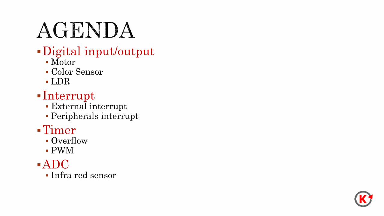
Digital input/output Motor Color Sensor LDR
Interrupt External interrupt Peripherals interrupt
Timer Overflow PWM
ADC Infra red sensor


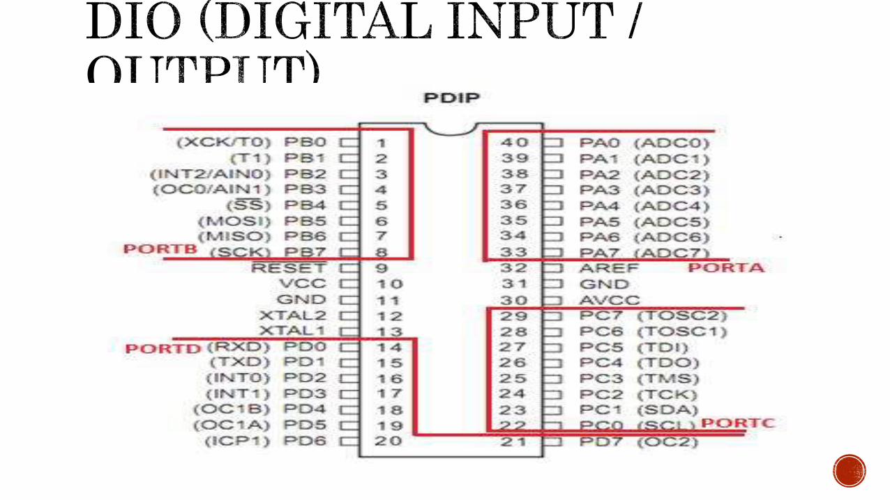
ATmega16 has 32 programmable I/O lines divided into 4 PORTS(groups): PORTA (PA0….PA7)
PORTB (PB0….PB7)
PORTC(PC0…..PC7)
PORTD(PD0…..PD7)
Each Port Can be controlled by 3 Register : DDRx(Data direction Register)
PORTx (Output Register)
PINx (Input Register)
Note : Most Pins of Microcontroller are multi-tasking (more than one function)(Multiplexed)


First we decide if the pin used as input or output
Then decide the direction of register using DDRx
0 for Input
1 for Output
In case we Read input from pin we use PINx register
In case we Write output on pin we use PORTx register

How to set values in Register :
DDRA = 0x55;
DDRA = 0b01010101;
DDRA = 5;

How to set value on specific pin without changing the other: To set the pin with 1 :
Make OR operation on the register with The pin no
Example: We want to set pin number 5 in PORTA with 1
PORTA=PORTA | (1<<PA5);
To set the pin with 0: Make AND operation on the register with (NOT) The pin no
Example: We want to set pin number 3 in PORTB with 0
PORTB=PORTB & ( ~ (1<<PB3) );
To toggle the pin : Make XOR operation on the register with The pin no
Example: We want to toggle pin number 2 in PORTC
PORTC=PORTC ^ (1<<PC2);

How to check on specific pin without checking the others:
To check if input on the pin is 1 : Make AND operation on the register with The pin no
Example: We check if pin number 5 in PORTA is 1
if (PORTA & (1<<PA5)){}
To check if input on the pin is 0 : Make AND operation on the register with The pin no and check if
equal zero OR Not the condition
Example: We check if pin number 5 in PORTA is 1
if ((PORTA & (1<<PA5)) == 0 ){}
if (!(PORTA & (1<<PA5))){}

Application:
Outputs:
Motors ( DC, Stepper, Servo).
LEDS.
LCD.
7 segment.
Inputs:Sensors.
Switch.
Keypad.
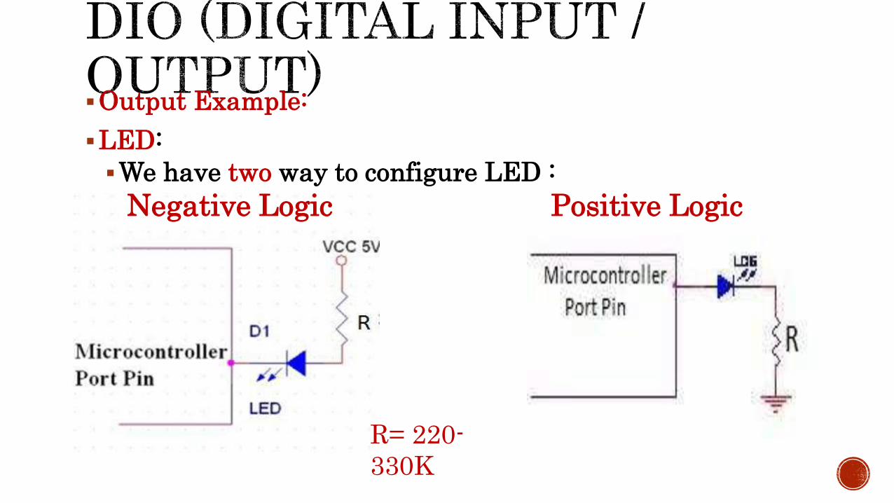
Output Example:
LED:
We have two way to configure LED :
Negative Logic Positive Logic
R= 220-
330K

Input Example:
Switch: We have two way to configure switch :
Pull-up Resistor Pull-down Resistor
R= 10K

Note Atmega16 provide internal pull up resistor for all port pins
In case you set any PIN as input you can activate the internal pull up resistor by setting the corresponding bit in PORTX register.
Example To set the pin 2 in PORTB as input pin and use the internal pull up resistor of this pin.
DDRB = DDRB & (~(1<<PB2));
PORTB= PORTB | (1<<PB2);
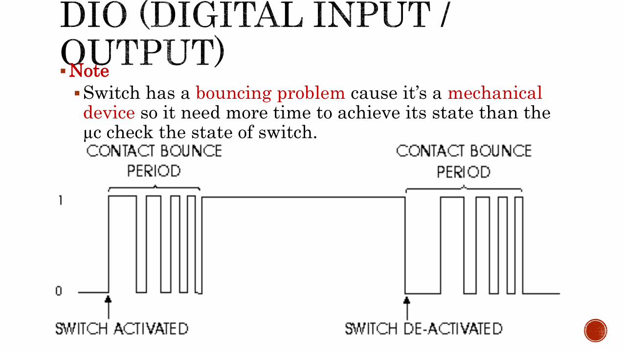
Note
Switch has a bouncing problem cause it’s a mechanical device so it need more time to achieve its state than the µc check the state of switch.
Due to this problem, we can solve it by software.
We can make a delay of 20-30 ms due to the fact that de-bounce maximum period takes this time.
The basic idea is to implement a delay after the first detected edge, during which no scanning for the switch is done. after the delay period is finished, scanning can proceed.

Motors:
Dc motor
Stepper motor
Servo motor

Dc Motor
It comes to speed, weight, size, cost... DC motors are always preferred over stepper motors.
Advantage:Control motion of robot.
Control its speed.
Control direction of its rotation.
Disadvantage:Hard to control its rotation angle.
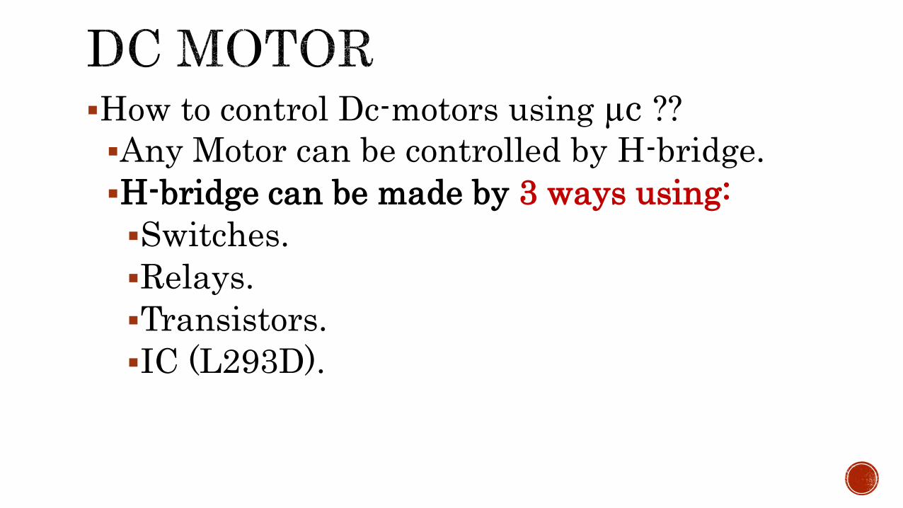
How to control Dc-motors using µc ??
Any Motor can be controlled by H-bridge.
H-bridge can be made by 3 ways using:
Switches.
Relays.
Transistors.
IC (L293D).

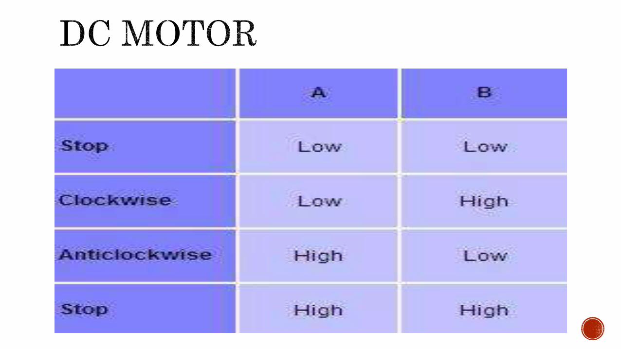
Working theory of H-bridge?
The name "H-Bridge" is derived from the actual shape of the switching circuit which control the motion of the motor. It is also known as "Full Bridge". Basically there are four switching elements in the H-Bridge as shown in the figure below.

Switches
Current flow when both high side left and low side right are switched on

Switches cont.

Using Transistor (BJT & Two pin from µc)

Using Transistor (BJT & Two pin from µc)
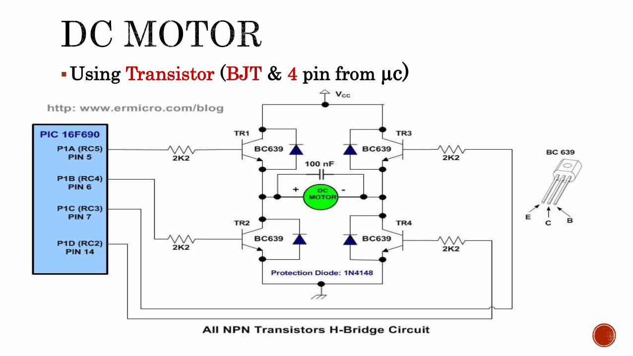
Using Transistor (BJT & 4 pin from µc)

Using H-bridge Most common chip to control Motor is
L293D
This chip can control 2 Dc motor
First DC Motor three µC pins are needed to control the DC motor (Input1, Input2, Enable1) and the motor connected to Output1 & Output2 pins.
Second DC Motor three µC pins are needed to control the DC motor (Input3, Input4, Enable2) and the motor connected to Output3 & Output4 pins.
Vss pin is connected to 5v.
Vs pin is connected to the Motor voltage 12v .


Types of stepper motor
Variable Reluctance
Permanent Magnet & Hybrid
Unipolar stepper motor (5,6 wires)
Bipolar stepper motor (4 wires)
Bifilar (8 wires)
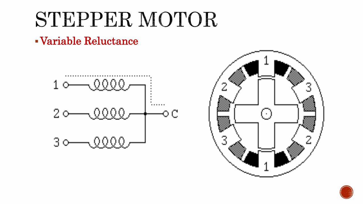
Variable Reluctance

Permanent Magnet & Hybrid
Unipolar (5 or 6 wires) Bipolar (4 wires)
Bifilar (8 wires)

How Stepper motors work ??
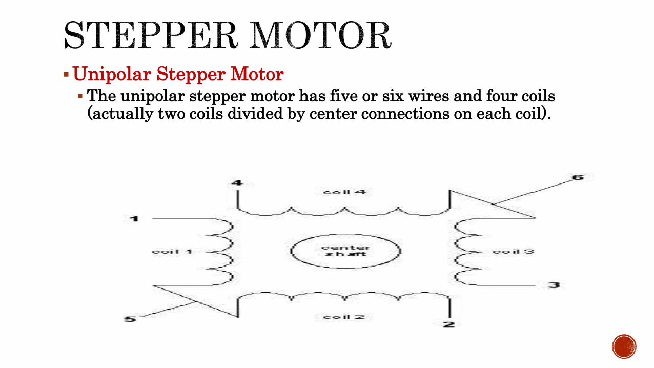
Unipolar Stepper Motor The unipolar stepper motor has five or six wires and four coils
(actually two coils divided by center connections on each coil).
Unipolar Stepper Motor
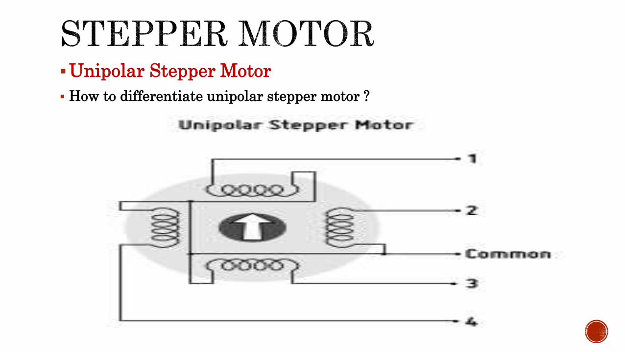
How to differentiate unipolar stepper motor ?

Unipolar Stepper Motor
How to control unipolar stepper motor using transistors?
Bipolar Stepper Motor
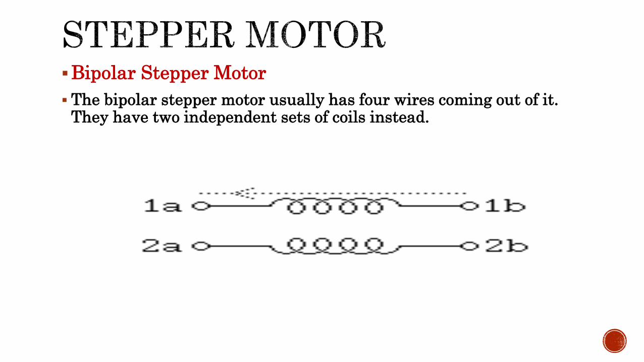
The bipolar stepper motor usually has four wires coming out of it. They have two independent sets of coils instead.
Bipolar Stepper Motor
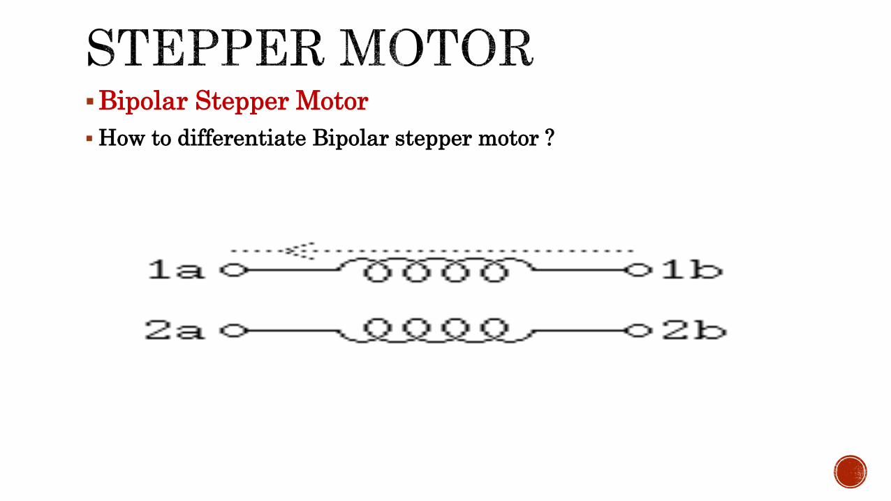
How to differentiate Bipolar stepper motor ?

Stepper motors drive sequences:
Full Step Sequence
Half Step Sequence

Step Angle
The angle traversed by the motor in one step.
To calculate step angle, simply divide 360 by number of steps a motor takes to complete one revolution.

Example
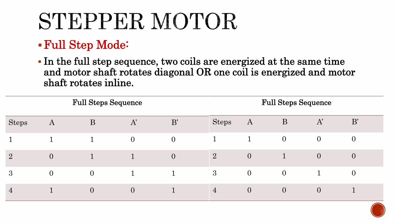
Full Step Mode:
In the full step sequence, two coils are energized at the same time and motor shaft rotates diagonal OR one coil is energized and motor shaft rotates inline.
Full Steps Sequence
Steps A B A’ B’
1 1 1 0 0
2 0 1 1 0
3 0 0 1 1
4 1 0 0 1
Full Steps Sequence
Steps A B A’ B’
1 1 0 0 0
2 0 1 0 0
3 0 0 1 0
4 0 0 0 1

Full Step Mode:

Half Step Mode :
In Half mode step sequence, motor step angle reduces to half the angle in full mode.
Half Mode Sequence
Step A B A\ B\
0 1 1 0 0
1 0 1 0 0
2 0 1 1 0
3 0 0 1 0
4 0 0 1 1
5 0 0 0 1
6 1 0 0 1
7 1 0 0 0

Half Step Mode :

Interfacing Unipolar Stepper Motor
Interface using L293D - H-Bridge Motor Driver
Interface using ULN2003/2004 - Darlington Arrays

Unipolar stepper using L293D:

Unipolar using ULN2003/2004

Unipolar Full step Mode (4 wires)

Unipolar Half step Mode (4 wires)
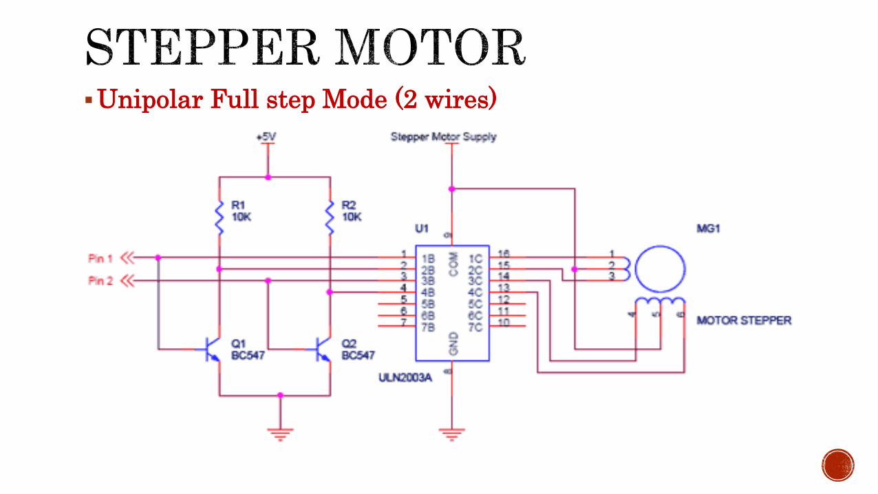
Unipolar Full step Mode (2 wires)
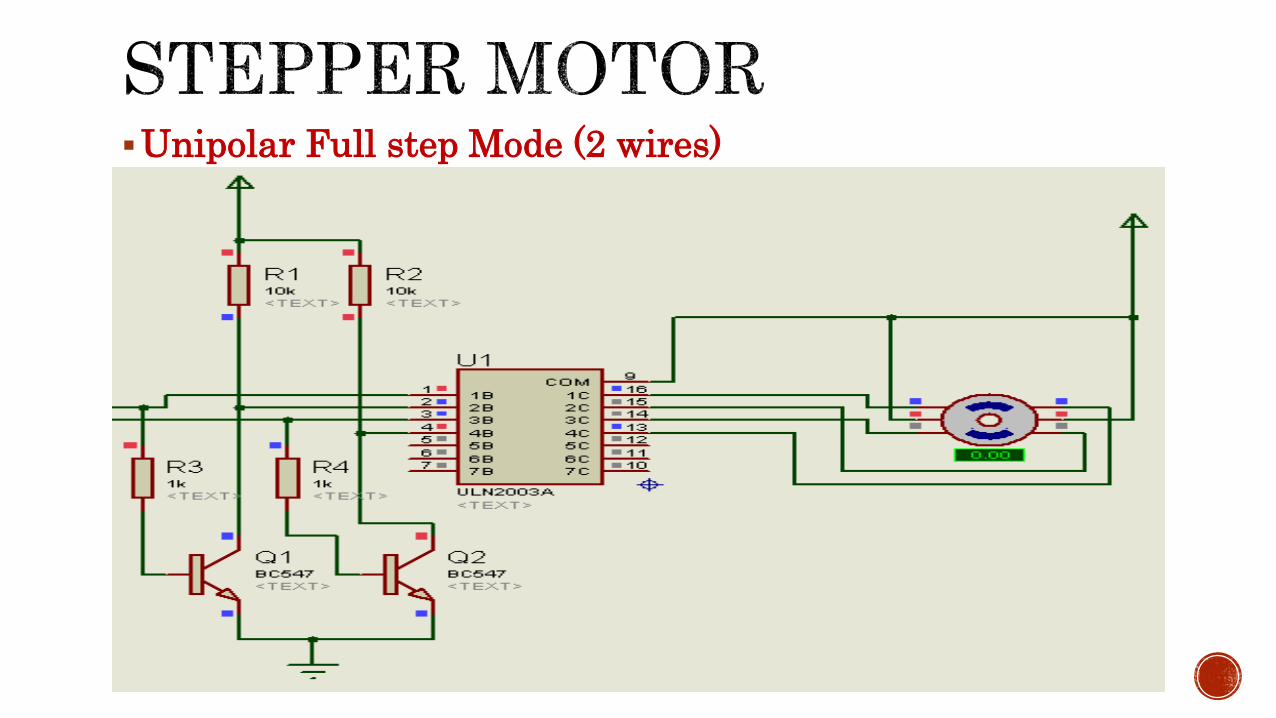
Unipolar Full step Mode (2 wires)

Bipolar Full step Mode (4 wires)

Servo or RC Servo Motors are DC motors equipped with a servo mechanism for precise control of angular position.
The RC servo motors usually have a rotation limit from 90° to 180°. Some servos also have rotation limit of 360°or more.
But servos do not rotate continually. Their rotation is restricted in between the fixed angles.
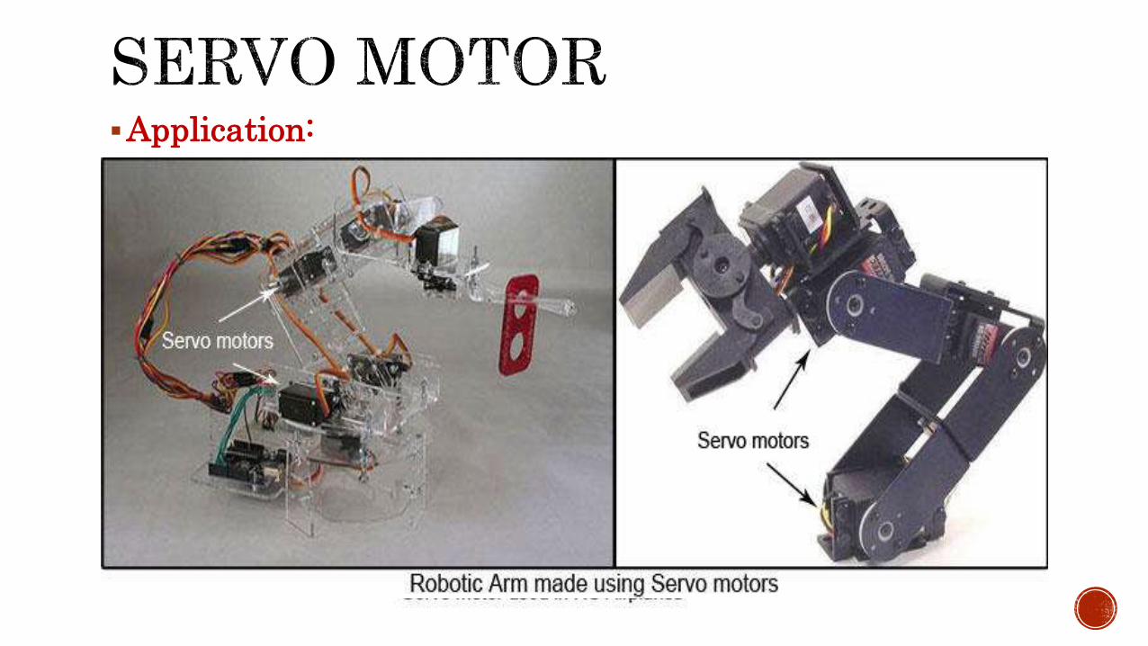
Application:
Servo concepts
The Servo Motors come with three wires or leads.
Two of these wires are to provide ground and positive supply to the servo DC motor.
The third wire is for the control signal.
The red wire is the DC supply lead and must be connected to a DC voltage supply in the range of 4.8 V to 6V.
The black wire is to provide ground.
The color for the third wire (to provide control signal) varies for different manufacturers. It can be yellow (in case of Hitec), white (in case of Futaba), brown etc.

NOTE :
Unlike DC motors, reversing the ground and positive supply connections does not change the direction (of rotation) of a servo.
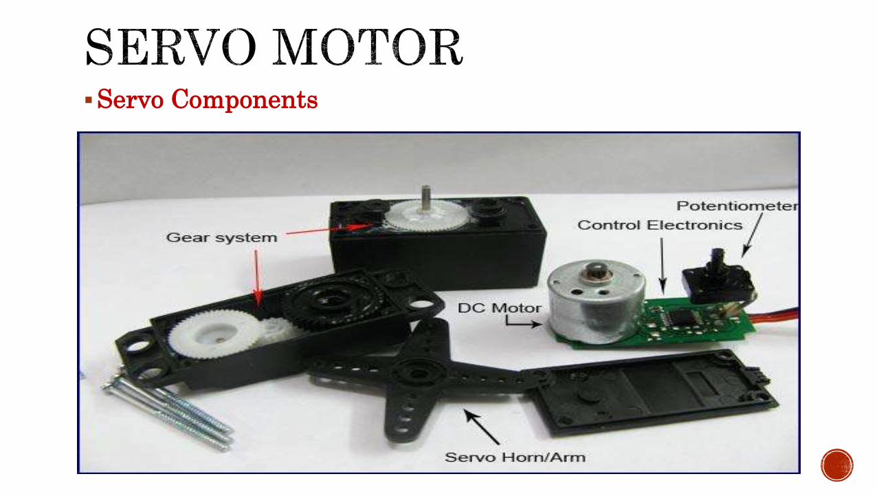
Servo Components

How Servo Works ??

Servo Connection

LDR: Sensor used to detect light and create voltage difference
Most common is photoresistor.
We use it in line following or detect object nearby.

How it works
It uses the principal that white color reflects lights & black color absorb light.

How it works
We connect to LDR to both sides and when :
S1 = S2 (in intensity of light) -> motor moves forward
S1= black (less intensity of light) -> Turn Left
S2=black (less intensity of light) ->Turn Right

How it works
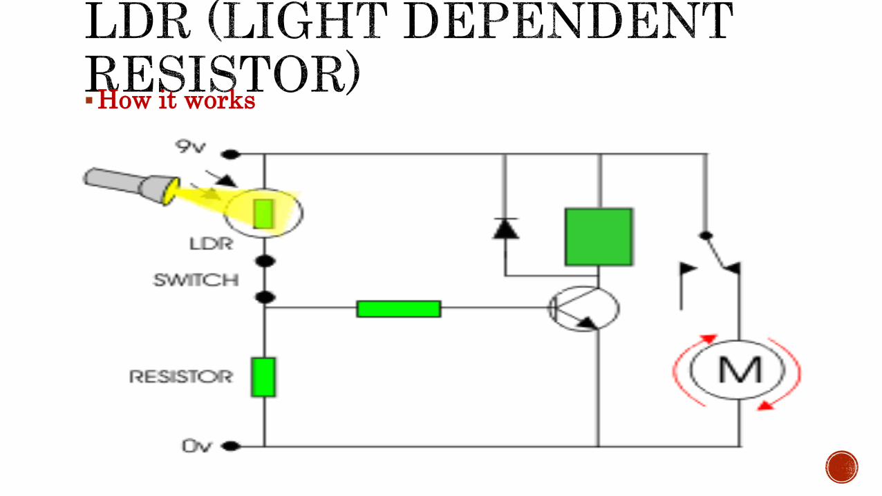
How it works


What’s Interrupts ?
Basically events that require immediate attention by the microcontroller.
An interrupt is a signal to the processor emitted by hardware or software indicating an event that needs immediate attention.
When an interrupt event occurs, the microcontroller pause its current task and attend to the interrupt by executing its corresponding Interrupt Service Routine (ISR) then microcontroller returns to the task it had pause and continue its normal operations.

Such an event may be:
An peripheral device has finished the last task it was given and is now ready for another. For example ADC may be generate interrupt after finishing the conversion from analog to digital.
External Interrupt event on I/O Pin.
An error from a peripheral.
You can think of it as a hardware-generated function call.

ISR (Interrupt service routine)
Piece of code that should be execute when an interrupt is triggered
Should be deterministic and short as possible, as it usually set a flag to a specific task indicating a certain event is happened, or save
small data in buffer.

AVR Interrupts
The AVR provides several different interrupt sources.
All interrupts are assigned individual enable bits to which must be written a logic one together with the Global Interrupt Enable bit in the Status Register in order to enable the interrupt.
Any Interrupt request is triggered by an event that sets its corresponding interrupt flag.


REMEMBER
Global interrupt enabled bit MUST be enabled for interrupts to be activated in the µC.
To Set global interrupt : sei(); // AVR microcontroller
SREG = SREG | (1<<7);
SREG = SREG | (1<<I);
To clear global interrupt : cli();
SREG = SREG & (~(1<<7));
SREG = SREG & (~(1<<I));
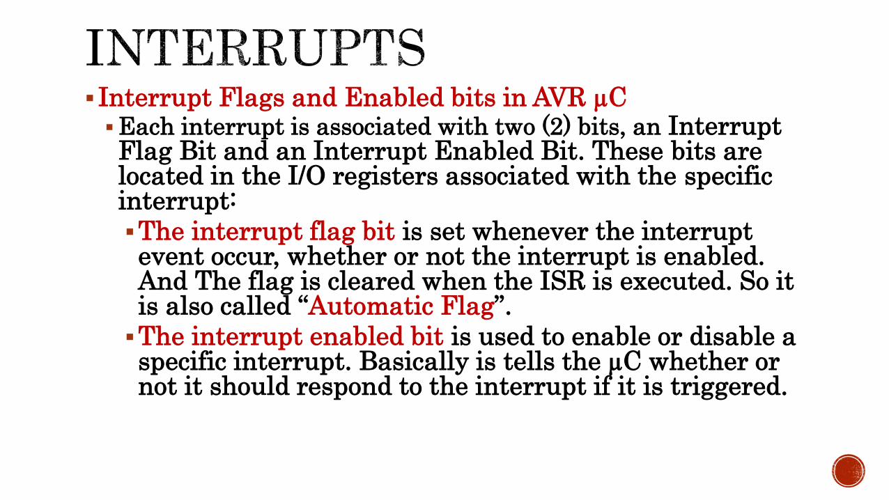
Interrupt Flags and Enabled bits in AVR µCEach interrupt is associated with two (2) bits, an Interrupt Flag Bit and an Interrupt Enabled Bit. These bits are located in the I/O registers associated with the specific interrupt:
The interrupt flag bit is set whenever the interrupt event occur, whether or not the interrupt is enabled. And The flag is cleared when the ISR is executed. So it is also called “Automatic Flag”.
The interrupt enabled bit is used to enable or disable a specific interrupt. Basically is tells the µC whether or not it should respond to the interrupt if it is triggered.

Global interrupt
Interrupt flag
Interrupt enabled
Interrupt Request

The AVR 8-bits microcontroller provide both internal and externalinterrupt sources.
The internal interrupts are associated with the microcontroller's peripherals like : Timer/Counter
Analog to Digital Converter,
USART
The external interrupts are triggered via external pins. for an AVR 8-bit microcontroller. On this microcontroller there are four (4) external interrupts: RESET interrupt : Triggered from pin 9. External Interrupt 0 (INT0) : Triggered from pin 16(PD2).
External Interrupt 1 (INT1) : Triggered from pin 17(PD3).
External Interrupt 2 (INT2) : Triggered from pin 3(PB2).

RESET interrupt It active low interrupt which means it triggered when low voltage (0 volt) is applied on reset pin (number 9).
Other 3 hardware interrupt are triggered by event that can be configured using I/O register.
If any of this interrupt is enabled and triggered , they are service by an ISR (Code) which is written by programmer.

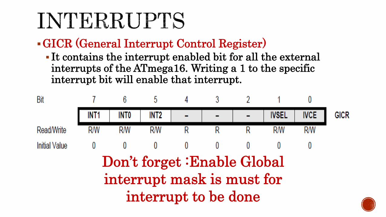
GICR (General Interrupt Control Register) It contains the interrupt enabled bit for all the external interrupts of the ATmega16. Writing a 1 to the specific interrupt bit will enable that interrupt.
Don’t forget :Enable Global
interrupt mask is must for
interrupt to be done

MCUCR (MCU Control Register)
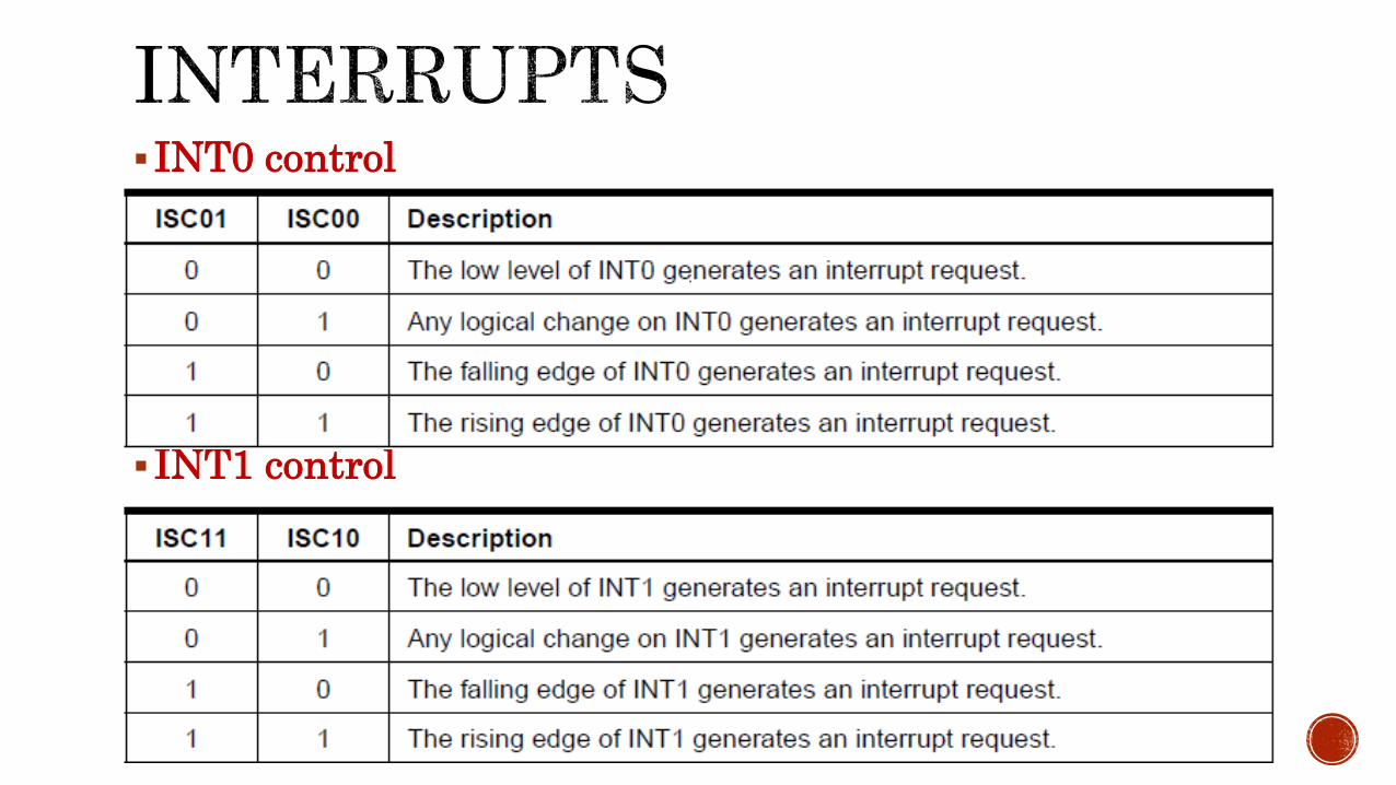
INT0 control
INT1 control

GIFR (General Interrupt Flag Register) The GIFR register contains the interrupt flags for all the
ATmega16 external interrupts. Each of these bit are set individually to logic 1 when the interrupt event for the specified interrupt occurs. Note that the flag bit of an interrupt is set, whether or not the interrupt is enabled, once the interrupt event occurs.
If the interrupt is enabled, it’s corresponding interrupt flag bit will be cleared after executing it’s ISR code.


Timer is special register that can be 8-16 bit so capable of holding from 0 to 255-65536
What differ it from any register that it count up / down automatically at predefined rate and this is Timer Clock that doesn’t need CPU intervention.
Timer Clock could be internal / external


One of basic condition when Timer overflow( it means timer counted up to its maximum value and return back to zero).
In this situation it causes interrupt and if global interrupt mask is enabled and timer interrupt enable so you have to write ISR to handle the event of the overflow

In case you want to increase the time needed for specific operation we use timer prescalar
Prescalar divide the clock frequency and produce timer clock
Prescalar modes are No prescalar (Timer Clock).
Clock/8.
Clock/64.
Clock/256.
Clock/512.
Clock/1024.
NO clock.
NoteCPU Clock doesn’t affected by
reduction using prescalar.
It remain the same

Example for using prescalar : If you using 1 MHZ for CPU Clock without using prescalar timer
takes to count up till it overflow 256 µs
But when you use prescalar 1024 timer takes to count up till it overflow 0.26 sec
It’s easy to know the time timer need to overflow if you know Resolution.
Resolution is the smallest period taken by timer to take one countwe can calculate it through formula
Resolution = (1/Frequency)
So if microcontroller is clocked with 1MHz source, then 8 bit timer without prescaler will run with resolution:
Resolution=1/1MHz=1µs

So if timer take 256 counts to overflow then it takes :
T= Resolution * 256 = 1µs *256 = 256 µs
And when we use 1024 as prescalar:
Resolution = 1024 / 1 MHZ = 1024µs
T = Resolution * 256 = 1024 * 256 = 0.256

ATmega16/32 have 3 Timer/counter we have three Timers/Counters each one with Separate Prescaler. Timer 0 - 8 bit timer.
Timer 1 -16 bit timer.
Timer 2 - 8 bit timer.
Timer also can be operated in 3 modes :Normal mode (Overflow).
Pulse Width Modulation mode(PWM).
Clear Timer Compare mode(CTC ).

Timer0Timer0 is an 8 bit timer/counter which can count from 0 to 0xFF (255).
In the timer mode this peripheral uses an internal clock signal.
In the counter mode an external signal on PIN0 in PORTB.
The timer can be operated either in the polling mode or in the interrupt mode.

Timer/Counter Control Register – TCCR0
Bit 7 – FOC0: Force Output Compare
The FOC0 bit is only active when the WGM00 bit specifies a non-PWM mode.
Bit 3, 6 – WGM01:0: Waveform Generation Mode
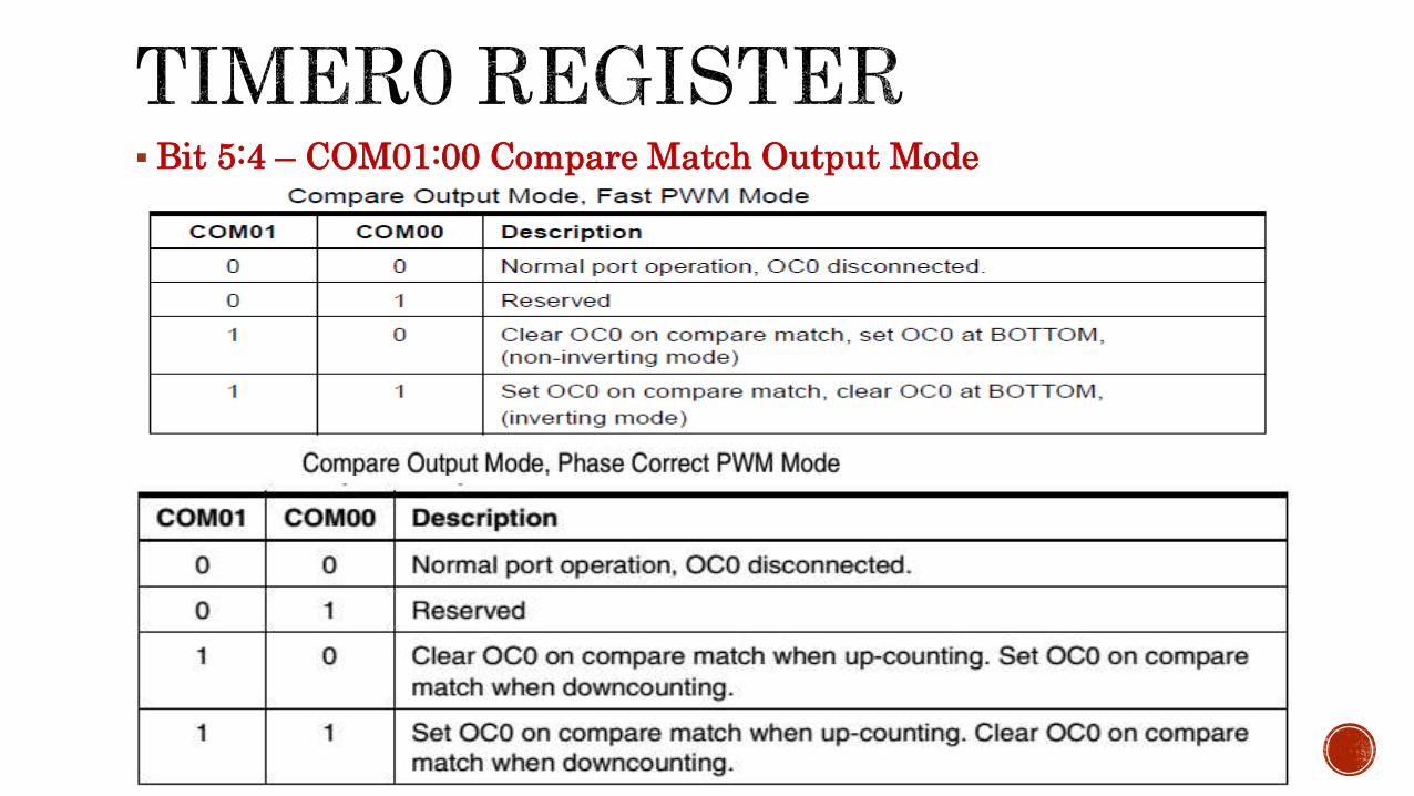
Bit 5:4 – COM01:00 Compare Match Output Mode

Bit 2:0 – CS02:0: Clock Select

Timer/Counter Register – TCNT0This is where the 8-bit counter of the timer resides. The value of the counter is stored here and it increases automatically each clock cycle. Data can be both read/written from this register. The initial value of the counter is set by writing it.

Output Compare Register – OCR0 The Output Compare Register contains an 8-bit value that is
continuously compared with the counter value (TCNT0). A match can be used to generate an output compare interrupt, or to generate a waveform output on the OC0 pin.

Timer/Counter Interrupt Mask Register –TIMSKTOIE0: Timer Overflow Interrupt Enable
OCIE0: Output Compare Match Interrupt Enable
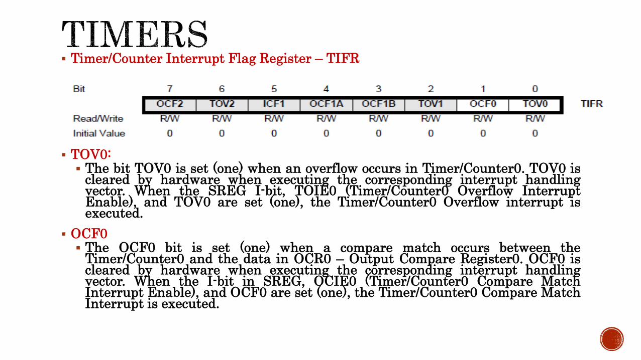
Timer/Counter Interrupt Flag Register – TIFR
TOV0: The bit TOV0 is set (one) when an overflow occurs in Timer/Counter0. TOV0 is
cleared by hardware when executing the corresponding interrupt handlingvector. When the SREG I-bit, TOIE0 (Timer/Counter0 Overflow InterruptEnable), and TOV0 are set (one), the Timer/Counter0 Overflow interrupt isexecuted.
OCF0 The OCF0 bit is set (one) when a compare match occurs between the
Timer/Counter0 and the data in OCR0 – Output Compare Register0. OCF0 iscleared by hardware when executing the corresponding interrupt handlingvector. When the I-bit in SREG, OCIE0 (Timer/Counter0 Compare MatchInterrupt Enable), and OCF0 are set (one), the Timer/Counter0 Compare MatchInterrupt is executed.
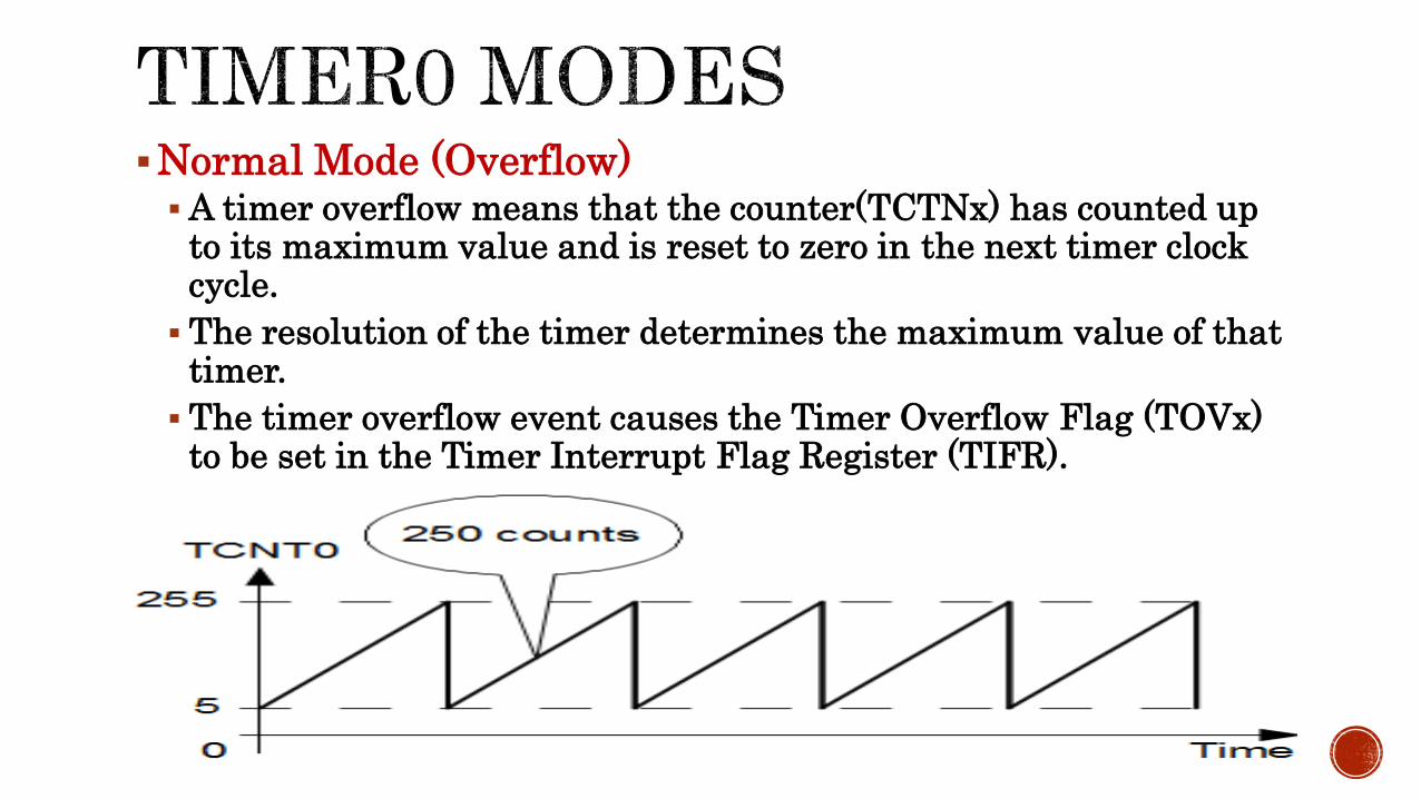
Normal Mode (Overflow) A timer overflow means that the counter(TCTNx) has counted up
to its maximum value and is reset to zero in the next timer clock cycle.
The resolution of the timer determines the maximum value of that timer.
The timer overflow event causes the Timer Overflow Flag (TOVx) to be set in the Timer Interrupt Flag Register (TIFR).
Timer compare mode :
In compare mode we load a register called Output Compare Register OCRx with a value of our choice and the timer will compare the current value of timer TCTNxwith that of Output Compare Register continuously and when they match the following things can be configured to happen: In Clear Timer on Compare mode (CTC) timer is configured to clear its count register TCNTx to “0” when matching occurs witthe output compare register OCRx.
A related Output Compare Pin can be made to go high, low or toggle automatically. This mode is ideal for generating square waves of different frequency.
It can be used to generate PWM signals used to implement a DAC digital to analog converter which can be used to control the speed of DC motors.
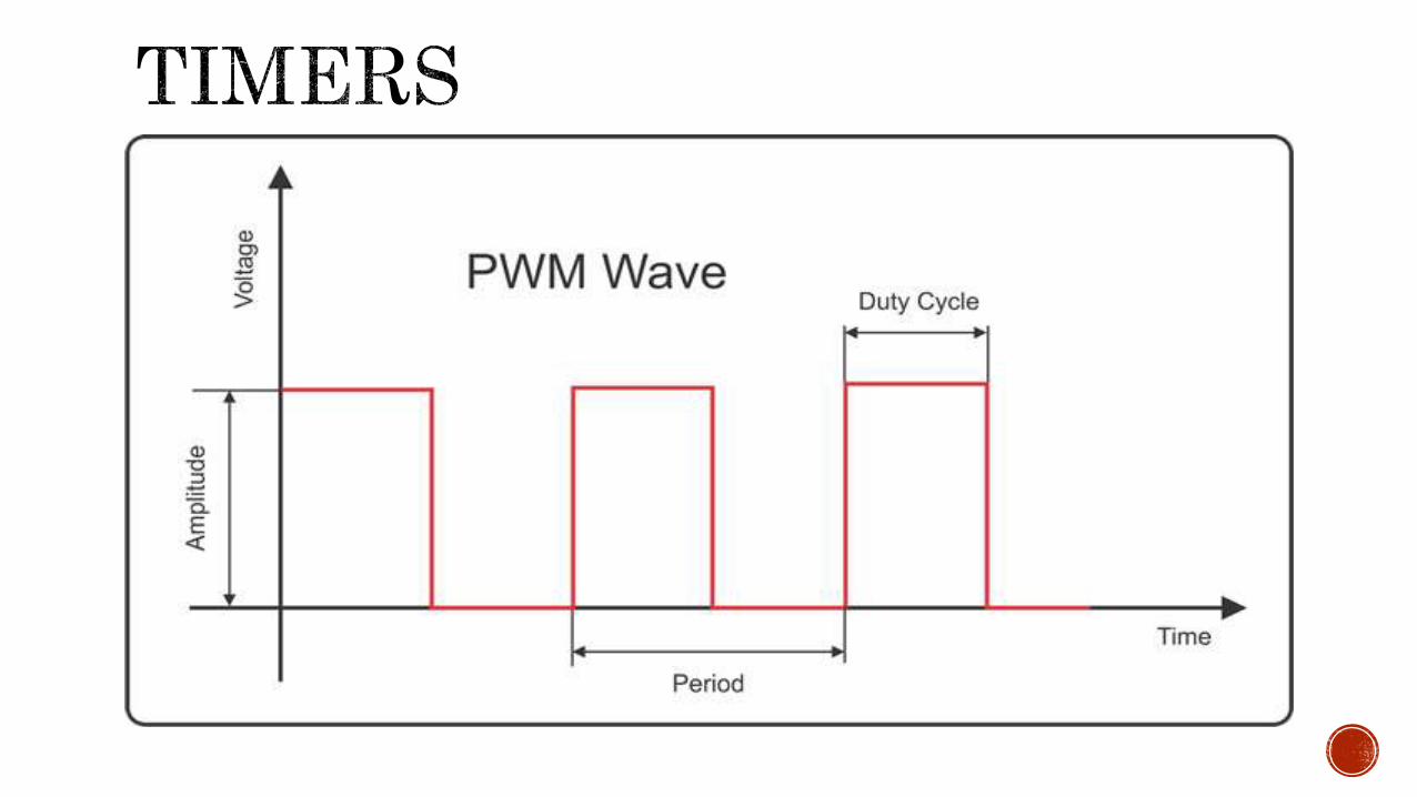
Pulse Width Modulation
is the technique used to generate analogue signals from a digital device like a MCU. Almost all modern MCUs have dedicated hardware for PWM signal generation.
A digital device, like a microcontroller can only generate two levels on its output lines, HIGH=5v and LOW=0V.
But what if we want to generate 2.5v or 3.1v or any voltage between 0-5 volt output ?
For these kinds of requirement, instead of generating a constant DC voltage output we generate a square wave, which has high = 5V and Low = 0v
We will use the simplest timer, TIMER0 for PWM generation.
Pulse Width Modulation
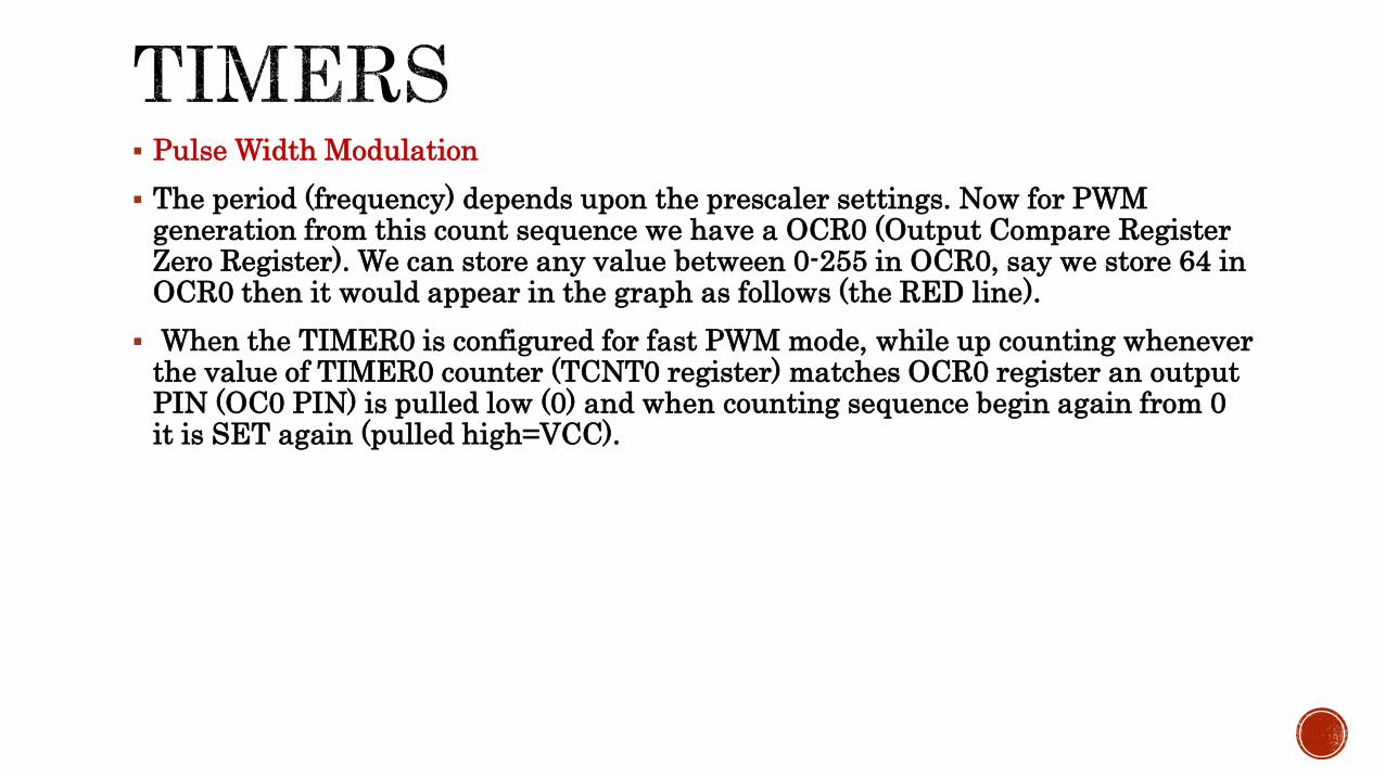
The period (frequency) depends upon the prescaler settings. Now for PWM generation from this count sequence we have a OCR0 (Output Compare Register Zero Register). We can store any value between 0-255 in OCR0, say we store 64 in OCR0 then it would appear in the graph as follows (the RED line).
When the TIMER0 is configured for fast PWM mode, while up counting whenever the value of TIMER0 counter (TCNT0 register) matches OCR0 register an output PIN (OC0 PIN) is pulled low (0) and when counting sequence begin again from 0 it is SET again (pulled high=VCC).

Pulse Width Modulation
Note:
to be able to generate
an output from the
PWM in Timer0, the
Output Compare Pin of
Timer0 (OC0) must
be set as output pin.
DDRB |= PB3


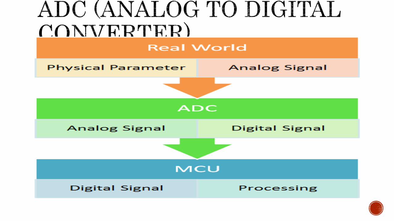
Most data around us is analog like voltage, pressure & temperature.
So we must process data received, and this operation is inaccurate, take much time also don’t give accurate results
So to solve this problem we have to convert analog signal to digital signal.
Since MCU is digital device so it can’t understand analog signal so it converts analog signal to digital and make many processes on it.
Embedded system use analog to digital module to collect data from external world (data acquisition system)
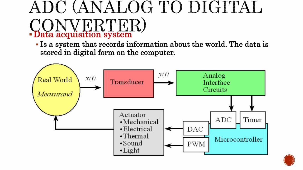
Data acquisition system Is a system that records information about the world. The data is
stored in digital form on the computer.

Signal(data) acquisition process
In general this process take 3 steps :
In the Real World, a sensor senses any physical parameter and converts into an equivalent analog electrical signal. Example temperature sensor.
For efficient and ease of signal processing, this analog signal is converted into a digital signal using an Analog to Digital Converter (ADC).
This digital signal is then fed to the Microcontroller (MCU) and is processed accordingly.

The ADC precision is the number of distinguishable ADC inputs that ADC can measure (e.g. 1024 alternatives for 10 bits ADC).
The ADC range is the maximum and minimum ADC input (e.g. 0 to +5V).
The ADC resolution is the smallest distinguishable change in input voltage that can be.
i.e. The resolution is the change in input that causes the digital output to change by 1.
𝑹𝒆𝒔𝒐𝒍𝒖𝒕𝒊𝒐𝒏 =𝑨𝑫𝑪 𝑹𝒂𝒏𝒈𝒆 (𝒗𝒐𝒍𝒕𝒔)
𝑨𝑫𝑪 𝒑𝒓𝒆𝒄𝒊𝒔𝒊𝒐𝒏=
𝟓−𝟎
𝟏𝟎𝟐𝟒= 𝟒. 𝟖𝟖𝒎𝒗
Don’t forgetAgain the goal of an analog to
digital converter is to take an
analog signal (0 to 5 V on our
microcontroller) and convert it to
a digital number (0 to 1024 on
our µC).

In general, sensors provide with analog output, but a MCU is a digital one. Hence we need to use ADC. We can straightaway use the inbuilt ADC of the MCU. In ATMEGA16/32, PORTA contains the ADC pins.
8 channel implies that there are 8 ADC pins are multiplexed together. You can easily see that these pins are located across PORTA (PA0…PA7).
10 bit resolution implies that the digital result from the ADC after converting the analog signal to digital is 10-bits and there are 2^10 = 1024 steps.
The type of ADC implemented inside the AVR MCU is of Successive Approximation type.
For example: Suppose we use a 5V reference. In this case, any analog value in between 0 and 5V is converted into its equivalent ADC value as shown above. The 0-5V range is divided into 2^10 = 1024 steps. Thus, a 0V input will give an ADC output of 0, 5V input will give an ADC output of 1023, whereas a 2.5V input will give an ADC output of around 512. This is the basic concept of ADC.


ADC Prescaler:
The ADC of the AVR converts analog signal into digital signal at some regular interval. This interval is determined by the clockfrequency. In general, the ADC operates within a frequency range of 50kHz to 200kHz. But the CPU clock frequency is much higher (in the order of MHz). So to achieve it, frequency division must take place. The prescaler acts as this division factor. It produces desired frequency from the external higher frequency. There are some predefined division factors –2, 4, 8, 16, 32, 64, and 128.
For example, a prescaler of 8 implies F_ADC = F_CPU/8. For F_CPU = 1MHz, F_ADC = 1M/8 = 125kHz.

ADMUX - ADC Multiplexer Selection Register
Bits 7:6 – REFS1:0 – Reference Selection Bits
These bits are used to choose the reference voltage. The following combinations are used.

Bit 5 – ADLAR – ADC Left Adjust Result
The ADLAR bit affects the presentation of the ADC conversion result in the ADC Data Register. Write one to ADLAR to left adjust the result. Otherwise, the result is right adjusted.

Bits 4:0 – MUX4:0 – Analog Channel and Gain Selection Bits
Used to choose between the 8 channel that can be used to take analog signal
These channel are found in PORTA (PA0..PA7)
Need to mention
Since there are 5 bits, it
consists of
2^5 = 32 different conditions
as follows. However, we are
concerned only with the first
8 conditions. Initially, all the
bits are set to zero.

ADCSRA – ADC Control and Status Register A
Bit 7 – ADEN – ADC Enable As the name says, it enables the ADC feature. Unless this is enabled,
ADC operations cannot take place across PORTA i.e. PORTA will behave as GPIO pins.
Bit 6 – ADSC – ADC Start Conversion Write this to ’1′ before starting any conversion. This 1 is written as long
as the conversion is in progress, When the conversion is complete, it returns to zero. Normally it takes 13 ADC clock pulses for this operation. But when you call it for the first time, it takes 25 as it performs the initialization together with it.

Bit 5 – ADATE – ADC Auto Trigger Enable
When this bit is written to one, Auto Triggering of the ADC is enabled. The ADC will start a conversion on a positive edge of the selected trigger signal. The trigger source is selected by setting the ADC Trigger Select bits, ADTS in SFIOR.
Bit 4 – ADIF – ADC Interrupt Flag
This bit is set when an ADC conversion completes and the Data Registers are updated. The ADC Conversion Complete Interrupt is executed if the ADIE bit and the I-bit in SREG are set. ADIF is cleared by hardware when executing the corresponding interrupt handling vector. Alternatively, ADIF is cleared by writing a logical one to the flag.

Bit 3 – ADIE – ADC Interrupt Enable
When this bit is set to ’1′, the ADC interrupt is enabled. This is used in the case of interrupt-driven ADC.
Bits 2:0 – ADPS2:0 – ADC Prescaler Select Bits
The prescaler (division factor between CPU clock frequency and the ADC clock frequency) is determined by selecting the proper combination from the following.

ADCL and ADCH – ADC Data Registers
The result of the ADC conversion is stored here. Since the ADC has a resolution of 10 bits, it requires 10 bits to store the result. Hence one single 8 bit register is not sufficient. We need two registers –ADCL and ADCH (ADC Low byte and ADC High byte) as follows. The two can be called together as ADC.

Thanks toEng/Mohamed Tarek
Eng/Ahmed Omara
