interference suppression techniques for millimeter-wave integrated · pdf fileinterference...
TRANSCRIPT

Interference suppression techniques for millimeter-waveintegrated receiver front endsLu, C.
Published: 24/11/2015
Document VersionPublisher’s PDF, also known as Version of Record (includes final page, issue and volume numbers)
Please check the document version of this publication:
• A submitted manuscript is the author's version of the article upon submission and before peer-review. There can be important differencesbetween the submitted version and the official published version of record. People interested in the research are advised to contact theauthor for the final version of the publication, or visit the DOI to the publisher's website.• The final author version and the galley proof are versions of the publication after peer review.• The final published version features the final layout of the paper including the volume, issue and page numbers.
Link to publication
Citation for published version (APA):Lu, C. (2015). Interference suppression techniques for millimeter-wave integrated receiver front ends Eindhoven:Technische Universiteit Eindhoven
General rightsCopyright and moral rights for the publications made accessible in the public portal are retained by the authors and/or other copyright ownersand it is a condition of accessing publications that users recognise and abide by the legal requirements associated with these rights.
• Users may download and print one copy of any publication from the public portal for the purpose of private study or research. • You may not further distribute the material or use it for any profit-making activity or commercial gain • You may freely distribute the URL identifying the publication in the public portal ?
Take down policyIf you believe that this document breaches copyright please contact us providing details, and we will remove access to the work immediatelyand investigate your claim.
Download date: 16. May. 2018

Interference Suppression Techniques for
Millimeter-Wave Integrated Receiver Front Ends
Chuang Lu

This work was supported by the FP7-project Par4CR as well as the CATRENE-RF2THzproject.
Interference Suppression Techniques for Millimeter-Wave Integrated Receiver Front Ends/ by Chuang LuEindhoven University of Technology.
A catalogue record is available from the Eindhoven University of Technology Library.ISBN: 978-90-386-3959-8
Copyright c©2015, Chuang Lu. All rights reserved.
Typeset with LATEX.

Interference Suppression Techniques forMillimeter-Wave Integrated Receiver Front Ends
PROEFSCHRIFT
ter verkrijging van de graad van doctor aan de Technische UniversiteitEindhoven, op gezag van de rector magnificus prof.dr.ir. F.P.T. Baaijens,voor een commissie aangewezen door het College voor Promoties, in het
openbaar te verdedigen op dinsdag 24 november 2015 om 16.00 uur
door
Chuang Lu
geboren te Shandong, China

Dit proefschrift is goedgekeurd door de promotoren en de samenstelling van de pro-motiecommissie is als volgt:
voorzitter: prof.dr.ir. A.C.P.M. Backx1e promotor: prof.dr.ir. P.G.M. Baltus2e promotor: prof.dr.ir. A.H.M. van Roermundcopromotor: dr.dipl.-phys. M.K. Matters-Kammererleden: prof.dr.ir. B. Nauta (University of Twente)
prof.dr.ir. P. Wambacq (Vrije Universiteit Brussel)prof.dr.ir. B. Smolders
adviseur: dr. Kave Kianush (Catena Microelectronics B.V.)
Het onderzoek of ontwerp dat in dit proefschrift wordt beschreven is uitgevoerd in overeen-stemming met de TU/e Gedragscode Wetenschapsbeoefening.


vi
CONTENTS
Contents
List of Abbreviations xiii
1 Introduction 1
1.1 Background . . . . . . . . . . . . . . . . . . . . . . . . . . . . . . . . . . . . 1
1.1.1 Millimeter-Wave Wireless Technologies . . . . . . . . . . . . . . . . . 1
1.1.2 Advancements in Silicon Technologies . . . . . . . . . . . . . . . . . 2
1.2 Millimeter-Wave Applications . . . . . . . . . . . . . . . . . . . . . . . . . . 2
1.2.1 High Data-Rate Communication . . . . . . . . . . . . . . . . . . . . 2
1.2.2 Millimeter-Wave Radar . . . . . . . . . . . . . . . . . . . . . . . . . 3
1.2.3 Ka-band Satellite Communication . . . . . . . . . . . . . . . . . . . 4
1.2.4 Fifth-Generation (5G) Cellular Communication . . . . . . . . . . . . 5
1.2.5 Millimeter-Wave Imaging and Spectroscopy . . . . . . . . . . . . . . 5
1.3 Interference Issues in Millimeter-Wave Applications . . . . . . . . . . . . . . 5
1.3.1 Spatial Interference . . . . . . . . . . . . . . . . . . . . . . . . . . . . 6
1.3.2 Self Interference . . . . . . . . . . . . . . . . . . . . . . . . . . . . . 7
1.4 Aim and Scope of the Thesis . . . . . . . . . . . . . . . . . . . . . . . . . . 8
1.5 Outline of the Thesis . . . . . . . . . . . . . . . . . . . . . . . . . . . . . . . 9
2 Robust Spatial Null-forming in Millimeter-Wave Phased Arrays 11
2.1 Introduction . . . . . . . . . . . . . . . . . . . . . . . . . . . . . . . . . . . . 11
2.2 Uniform Linear Array Principles . . . . . . . . . . . . . . . . . . . . . . . . 12
vii

CONTENTS
2.2.1 Beam-Steering . . . . . . . . . . . . . . . . . . . . . . . . . . . . . . 12
2.2.2 Null-Forming . . . . . . . . . . . . . . . . . . . . . . . . . . . . . . . 15
2.3 Practical Degradations to Analog/RF Null-Forming Arrays . . . . . . . . . 17
2.4 Genetic Algorithm Assisted Robust Null-forming Array . . . . . . . . . . . 22
2.4.1 Proposed Method . . . . . . . . . . . . . . . . . . . . . . . . . . . . . 23
2.4.2 Adaptable MSB and LSB . . . . . . . . . . . . . . . . . . . . . . . . 25
2.4.3 Antenna Selection . . . . . . . . . . . . . . . . . . . . . . . . . . . . 25
2.4.4 The Summary of the Combined Method . . . . . . . . . . . . . . . . 26
2.5 Simulation Results . . . . . . . . . . . . . . . . . . . . . . . . . . . . . . . . 27
2.5.1 Array Pattern Simulations . . . . . . . . . . . . . . . . . . . . . . . . 27
2.5.2 Statistical SINR Simulations for an Indoor Scenario . . . . . . . . . 32
2.5.3 Conclusions for Simulation Results . . . . . . . . . . . . . . . . . . . 37
2.6 Phase Shifter and VGA Resolution Consideration . . . . . . . . . . . . . . . 37
2.7 Summary and Conclusions . . . . . . . . . . . . . . . . . . . . . . . . . . . . 40
3 High Resolution Phase Shifters for Null-Forming Phased Arrays 43
3.1 Introduction . . . . . . . . . . . . . . . . . . . . . . . . . . . . . . . . . . . . 43
3.2 State-of-the-Art . . . . . . . . . . . . . . . . . . . . . . . . . . . . . . . . . . 43
3.3 A 60 GHz Sliding-IF Front-End Architecture . . . . . . . . . . . . . . . . . 45
3.4 LO-Path Phase Shifter . . . . . . . . . . . . . . . . . . . . . . . . . . . . . . 46
3.4.1 Architecture . . . . . . . . . . . . . . . . . . . . . . . . . . . . . . . 46
3.4.2 Circuit Description . . . . . . . . . . . . . . . . . . . . . . . . . . . . 48
3.4.3 Measurement Results . . . . . . . . . . . . . . . . . . . . . . . . . . 53
3.5 Baseband Phase Shifter . . . . . . . . . . . . . . . . . . . . . . . . . . . . . 61
3.5.1 Architecture . . . . . . . . . . . . . . . . . . . . . . . . . . . . . . . 61
3.5.2 Circuit Description . . . . . . . . . . . . . . . . . . . . . . . . . . . . 61
3.5.3 Measurement Results . . . . . . . . . . . . . . . . . . . . . . . . . . 63
viii

CONTENTS
3.6 Benchmarking and Performance Summary . . . . . . . . . . . . . . . . . . . 66
3.7 Summary and Conclusions . . . . . . . . . . . . . . . . . . . . . . . . . . . . 69
4 Filtering LNA for Self-Interference Suppression 71
4.1 Introduction . . . . . . . . . . . . . . . . . . . . . . . . . . . . . . . . . . . . 71
4.2 Challenge of Full-Duplex Operation in VSAT . . . . . . . . . . . . . . . . . 72
4.3 Literature Review . . . . . . . . . . . . . . . . . . . . . . . . . . . . . . . . 76
4.4 Design Description . . . . . . . . . . . . . . . . . . . . . . . . . . . . . . . . 77
4.4.1 Trade-off Between Filtering and Noise Figure Degradation . . . . . . 77
4.4.2 Series or Parallel LC Resonance Filter . . . . . . . . . . . . . . . . . 80
4.4.3 Filtering Low Noise Amplifier Design . . . . . . . . . . . . . . . . . . 81
4.4.4 Reference Low Noise Amplifier Design without Filtering . . . . . . . 82
4.4.5 Layout Design . . . . . . . . . . . . . . . . . . . . . . . . . . . . . . 83
4.5 Simulation and Measurement Results . . . . . . . . . . . . . . . . . . . . . . 84
4.6 Benchmarking and Performance Summary . . . . . . . . . . . . . . . . . . . 90
4.7 Summary and Conclusions . . . . . . . . . . . . . . . . . . . . . . . . . . . . 93
5 Hybrid-Transformer Based Duplexer for Self-Interference Suppression 95
5.1 Introduction . . . . . . . . . . . . . . . . . . . . . . . . . . . . . . . . . . . . 95
5.2 Literature Review . . . . . . . . . . . . . . . . . . . . . . . . . . . . . . . . 96
5.3 Hybrid-Transformer Based Dual-Antenna Duplexer . . . . . . . . . . . . . . 97
5.3.1 Hybrid-Transformer Based Duplexer . . . . . . . . . . . . . . . . . . 97
5.3.2 Using Identical Antennas . . . . . . . . . . . . . . . . . . . . . . . . 98
5.3.3 Using Orthogonal Linearly-Polarized Antennas . . . . . . . . . . . . 98
5.4 Alternative Dual-Antenna Duplexer Using Rat-Race Coupler . . . . . . . . 102
5.5 30 GHz Duplexer Prototype . . . . . . . . . . . . . . . . . . . . . . . . . . . 102
5.6 Design of the On-Chip Tunable Hybrid-Transformer-Based Duplexer . . . . 103
5.6.1 Tunable Hybrid-Transformer . . . . . . . . . . . . . . . . . . . . . . 103
ix
CONTENTS
5.6.2 Low Noise Amplifier . . . . . . . . . . . . . . . . . . . . . . . . . . . 106
5.6.3 The Implemented IC . . . . . . . . . . . . . . . . . . . . . . . . . . . 107
5.7 Design of the Demonstrator with On-Board Antennas . . . . . . . . . . . . 108
5.7.1 Sequentially-Rotated Circularly-Polarized Patch Antenna . . . . . . 108
5.7.2 Wire-Bond Interface . . . . . . . . . . . . . . . . . . . . . . . . . . . 109
5.8 Measurement Results . . . . . . . . . . . . . . . . . . . . . . . . . . . . . . . 111
5.8.1 On-Chip Duplexer Measurement Results . . . . . . . . . . . . . . . . 111
5.8.2 Demonstrator Measurement Results . . . . . . . . . . . . . . . . . . 117
5.9 Discussions on Potential Extensions . . . . . . . . . . . . . . . . . . . . . . 120
5.10 Summary and Conclusions . . . . . . . . . . . . . . . . . . . . . . . . . . . . 121
6 Conclusions and Recommendations 123
6.1 Conclusions . . . . . . . . . . . . . . . . . . . . . . . . . . . . . . . . . . . . 123
6.2 Original Contributions . . . . . . . . . . . . . . . . . . . . . . . . . . . . . . 125
6.3 Recommendations for Future Work . . . . . . . . . . . . . . . . . . . . . . . 125
Appendix A. Phase Shift and Time Delay 127
Appendix B. Genetic Algorithm for the Null-Forming Array 131
Appendix C. Effective Reactance of Resonance Notch Filters 135
Bibliography 144
Summary 145
Samenvatting 147
List of Publications 149
Acknowledgements 151
x

CONTENTS
Biography 153
xi

CONTENTS
xii

List of Abbreviations
ACMA Aperture-Coupled Microstrip AntennaAoA Angle of ArrivalAR Axial RatioBBPS Base-Band Phase ShifterCCDF Complementary Cumulative Distribution FunctionCCI Co-Channel Interference(Bi)CMOS (Bipolar) Complementary Metal Oxide SemiconductorCP Circularly PolarizedCPW Co-Planar WaveguideEM ElectromagneticFD2, FD4 Frequency Divider-by-2/4FDD Frequency Division DuplexGA Genetic AlgorithmHP Horizontally PolarizedICP Input Compression PointIF Intermediate FrequencyIIP3 Third Order Input Intercept PointIQ In-Phase and QuadratureLC Inductor and CapacitorLHCP Left-Handed Circular PolarizationLNA Low-Noise-AmplifierLOPS Local-Oscillator Path Phase Shifter(N)LOS (Non-)Line-of-SightLP Linearly Polarizedmm-Wave Millimeter-WaveMSB/LSB Most/Least Significant BitNF Noise FigurePA Power AmplifierPS Phase ShifterPSA Phase Selection AmplifierRF Radio FrequencyRHCP Right-Handed Circular Polarization

RX ReceiverSiGe (Silicon Germanium)SINR Signal-to-Interference-plus-Noise RatioSNR Singal-to-Noise RatioTline Transmission LineTX TransmitterULA Uniform Linear ArrayVGA Variable Gain AmplifierVP Vertically PolarizedVSAT Very-Small-Aperture TerminalWLAN/WPAN Wireless Local/Personal Area Network
Chapter 1
Introduction
1.1 Background
1.1.1 Millimeter-Wave Wireless Technologies
Since the first experiments and demonstrations on transmitting and receiving electromag-netic waves in the late nineteenth century [1], wireless technology has been developingfor over a century. Nowadays, the advancements in wireless technology have influencedin many aspects the way people live, work and communicate. Friends and families areable to talk and see each other on a 3G/4G enabled hand-held device no matter how farapart; drivers can immediately start an unfamiliar journey with the help of the globalpositioning systems (GPS) without worrying about the routes; Wireless Local/PersonalArea Networks (WLAN, WPAN) significantly facilitates peoples life by assuring the seam-less connectivity between devices and to the internet and/or the cloud; Wireless SensorNetworks (WSN) are able to monitor the environment, housing, machines’ condition andeven people’s health. There are many more examples that can be listed on how wirelesstechnologies have penetrated into our life.
All these advancements have lead to a congested radio spectrum for the currentlypopular wireless technologies, i.e. below 10 GHz. The available bandwidth in the currentlypopular frequency bands starts to hamper the constantly growing demand on higher datarate from the market. On the other hand, at millimeter-wave (mm-wave) frequencies,i.e. 30 GHz to 300 GHz, there is a comparably large amount of spectrum available. Thewider bandwidth can support multi-Gbps data-rate, which is very challenging to achieveat conventional RF frequencies below 10 GHz.
Other than the wider bandwidth, another advantage that can be offered in the mm-wave range is the system compactness. Due to the shorter wavelength at these frequencies,antennas are smaller than at lower frequencies. As a result, more compact systems can beenvisioned, like for phased array systems.
1

CHAPTER 1. INTRODUCTION
1.1.2 Advancements in Silicon Technologies
The advantages of the mm-wave applications, however, should be supported by high per-formance and in-expensive technologies in order to open the consumer’s market. Tradi-tionally, mm-wave systems were implemented in III-V compound-based technologies [2, 3].While these technologies offer higher operation frequency and high performance (in termsof gain, noise figure, power level etc.), they are expensive and suffer from limited fabri-cation yield [4]. As a result, these technologies typically are limited to professional ormilitary applications. In order for mm-wave systems to have mass deployment and meetconsumer market requirements, the cost and size of any solution has to be significantlybelow what is being achieved using III-V semiconductor technologies. Over the last fewdecades, silicon technologies (SiGe BiCMOS and CMOS) have driven the manufacturingcost significantly lower for high volume production. Furthermore, advanced silicon pro-cesses are able to offer reasonable performance for mm-wave applications [5, 6]. Thanksto the continuous scaling of CMOS and BiCMOS technologies, e.g. 90/65/40 nm CMOSand 0.18/0.13 µm BiCMOS, good performance can be achieved for commercial mm-waveapplications with low cost in high volume production.
The possibility of silicon-based mm-wave systems has triggered significant interestfrom the academia and industry in the last decade: fully integrated mm-wave systems aredemonstrated [7, 8]; techniques are developed to achieve performance in silicon which iscomparable to the III-V technologies [9, 10]; several standards regulations are published formm-wave applications [11, 12, 13]; and various mm-wave products in silicon technologieshave been launched into the market [14, 15].
1.2 Millimeter-Wave Applications
1.2.1 High Data-Rate Communication
One of the most exciting mm-wave bands in recent years is the unlicensed 60 GHz band.In 2001, the US Federal Communications Commission (FCC) announced a continuous 7GHz bandwidth around 60 GHz as an unlicensed band. Similar regulations are approvedin other parts of the world, e.g. in Europe, the spectrum allocation is about 9 GHz. Com-paring to some of the cellular bands and WLAN bands at 2.4 GHz and 5 GHz (of whichthe bandwidths are in the order of 10 MHz to 100 MHz), the spectrum available fromthe 60 GHz band is significantly wider, as shown in Fig. 1.1(a). Such a wide spectrum isattractive for multi-Gbps applications, which are magnitudes of order faster than the cur-rently popular bands. Examples include uncompressed video streaming, ultra-high-speedfile transfer/sync between personal devices and high-speed internet access. Some of theseare visualized in Fig. 1.1(b). Several standards targeting this band are developed, includ-ing IEEE 802.15.3c [11] for the WPAN applications, IEEE 802.11ad [12] for the WLANapplications and WirelessHD [16] for short-range high-definition multimedia transmission.Due to the higher path loss at mm-wave frequency range, multiple antennas (or phasedarrays) are typically applied in mm-wave systems to provide additional antenna gain andsatisfy the link budget. The use of phased array technique also offers the possibility of spa-tial reuse, because directive beams are used for transmission and reception. In addition,
2
1.2. MILLIMETER-WAVE APPLICATIONS
60 GHz10 GHz
2.1 GHz 2.4 GHz 5 GHzLTEband
IEEE802.11band
IEEE802.11band
≈ 0
.1 G
Hz
≈ 0
.1 G
Hz
≈ 0
.4 G
Hz
≈ 9 GHz
57 GHz 66 GHz60 GHz Spectrum Allocation in EU
(a)
(b)
Figure 1.1: (a) Spectrum allocation of the 60 GHz band in Europe, in comparison to theLTE cellular band and the IEEE 802.11 bands around 2.4 GHz and 5 GHz; (b) Typicalapplications of 60 GHz indoor communication.
the lower penetration through walls and high oxygen absorption at 60 GHz also increasethe frequency re-use.
1.2.2 Millimeter-Wave Radar
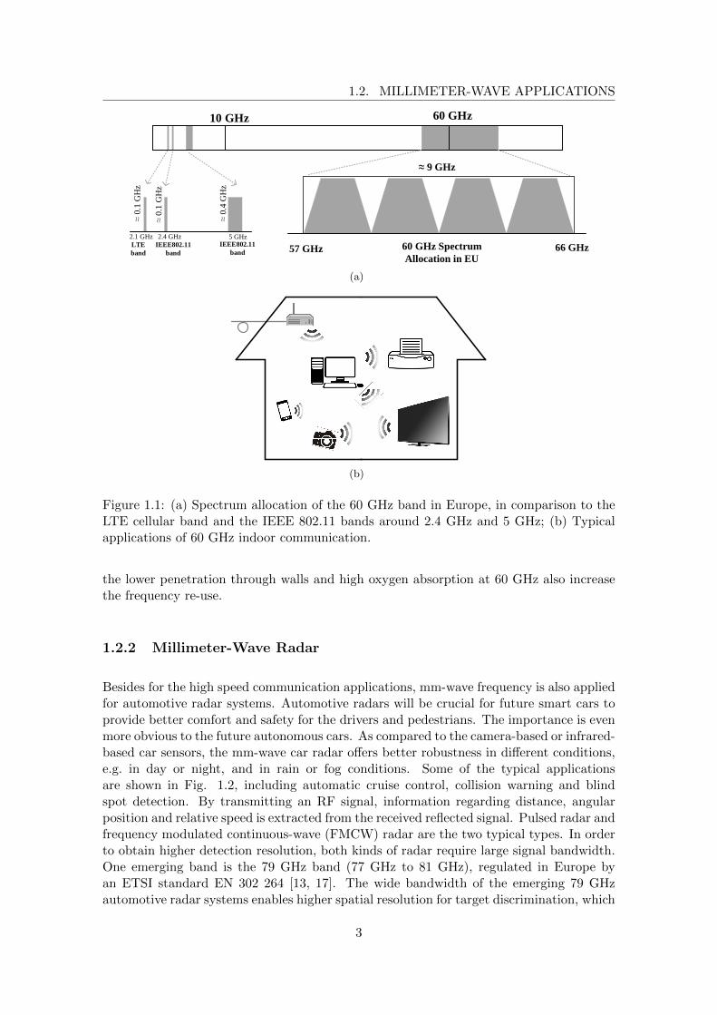
Besides for the high speed communication applications, mm-wave frequency is also appliedfor automotive radar systems. Automotive radars will be crucial for future smart cars toprovide better comfort and safety for the drivers and pedestrians. The importance is evenmore obvious to the future autonomous cars. As compared to the camera-based or infrared-based car sensors, the mm-wave car radar offers better robustness in different conditions,e.g. in day or night, and in rain or fog conditions. Some of the typical applicationsare shown in Fig. 1.2, including automatic cruise control, collision warning and blindspot detection. By transmitting an RF signal, information regarding distance, angularposition and relative speed is extracted from the received reflected signal. Pulsed radar andfrequency modulated continuous-wave (FMCW) radar are the two typical types. In orderto obtain higher detection resolution, both kinds of radar require large signal bandwidth.One emerging band is the 79 GHz band (77 GHz to 81 GHz), regulated in Europe byan ETSI standard EN 302 264 [13, 17]. The wide bandwidth of the emerging 79 GHzautomotive radar systems enables higher spatial resolution for target discrimination, which
3

CHAPTER 1. INTRODUCTION
Auto Cruise Control
Collision warning
Collision warning
Blind spot detection
Parking aid
Lane change assistance
Figure 1.2: Automotive radar applications using mm-wave frequency.
Gateway
Internet
Enterprise
Consumer Broadband
Cellular Backhaul
Downlink around20 GHz
Uplink around30 GHz
Figure 1.3: Ka-band VSAT applications.
offers higher reliability and safety.
1.2.3 Ka-band Satellite Communication
Very-small-aperture terminal (VSAT) is another mm-wave application. By means of satel-lite connections, VSATs are typically used for broadband internet access, rural area net-work access, enterprise communication etc. , as shown in Fig. 1.3. While today’s VSATsystems operate in the C-band (downlink at about 4 GHz and uplink at about 6 GHz) orKu-band (12 GHz downlink and 14 GHz uplink), the next generation will use Ka-band (20GHz downlink and 30 GHz uplink) to improve bandwidth and data rate [18], also referredto as high throughput satellite (HTS). Besides, Ka-band VSAT is also equipped with morea compact antenna. On the other hand, the Ka-band VSAT suffers from a higher rainfade effect which degrades quality of service. In this case, more power might be requiredto compensate the rain effect.
4
1.3. INTERFERENCE ISSUES IN MILLIMETER-WAVE APPLICATIONS
1.2.4 Fifth-Generation (5G) Cellular Communication
In recent years, we have witnessed an incredible growth of mobile data communication.It is even envisioned that the cellular networks may need to deliver as much as thousandtimes of the current capacity [19]. Today’s cellular providers strive to deliver higher speedand quality for wireless devices, but they are limited to a carrier frequency spectrumwhich only offers limited available bandwidth. Amongst other potential technologies, suchas massive multiple-input-multiple-output (MIMO) technology [20], utilizing the widerbandwidth of the mm-wave bands is one of the most promising directions for the fifthgeneration (5G) cellular networks [21]. Recent research has demonstrated the feasibility ofmm-wave cellular communications [19, 21], at 28 GHz and 38 GHz frequencies. Throughthe propagation measurements conducted in urban environments, continuous coveragecan be achieved with a cell radius of 200 meters, with the potential of offering an orderof magnitude increase in capacity over current fourth generation (4G) networks. Phasedarray technique is important in this case to incorporate the sensitivity to physical blockagesand achieve a good coverage.
1.2.5 Millimeter-Wave Imaging and Spectroscopy
Imaging at mm-wave frequencies, e.g. at 94 GHz, has also drawn lots of interest inresearch and industry for applications ranging from security detection to spectroscopyand bio-imaging. Unlike mm-wave communications, the principle of mm-wave imaging isbased on radiation, reflection or absorption from/by the object. Comparing to imagingtechnologies at the other electromagnetic spectrums, such as the visual spectrum, mm-wave imaging has the advantages of being able to operate in different conditions, betterrobustness, and good resolution. Furthermore, it is harmless to humans. While III-Vcompound technologies were traditionally used in imaging systems, silicon technologies onthe other hand can offer a low-power, fully-integrated and compact solution for mm-waveimaging systems. There have been many recent advances in this field [22].
1.3 Interference Issues in Millimeter-Wave Applications
Given the exciting and emerging applications and the availability of silicon technologiesfor mm-wave frequencies, we can envision that mm-wave systems will become popular andcommon in the future. As the number of mm-wave devices, systems or standards will growdramatically in the future, interference issues will become important for the co-existenceof different devices.
In the past decades, we have witnessed the rapid growth of devices in the lower fre-quency range, e.g. in cellular and WLAN applications. Interference has been an issue sincethe early stages of these applications, and has become even more important today. Beforedescribing the potential interference issues in mm-wave systems, it is worthwhile to brieflyreview the issues in the currently popular systems at lower frequencies. Two main typesof interference can be impacting the reception of the desired signal.
5

CHAPTER 1. INTRODUCTION
Desired TX
Desired RX
Co-located TX
Interference TX
Figure 1.4: Simplified and generalized illustration of interference scenarios in mm-waveradios.
Firstly and most commonly, the interference can be from other systems. Due to theexistence of multiple radio’s, out-of-band or in-band interference can be picked up bythe desired receiver, desensitizing or saturating the receiver. Conventional narrow-bandreceivers make use of external filters to suppress out-of-band interference and are at thesame time designed with high linearity to cope with the potential in-band interference.For the multi-standard and multi-band systems nowadays, wide-band receivers that areresilient to interference become important and even more challenging [23].
Secondly, interference can also come from the co-located transmitter from the samesystem, called self interference. In a single device or system, the transmitter and receivercan be operating at the same time, e.g. in frequency division duplexer (FDD) transceiversand multi-radio systems. Due to limited isolation, there can be high signal power leakageto the receiver, resulting in saturation or even causing damage to the receiver front end.Frequency domain filtering is generally used to reject the undesired leakage, for instance byoff-chip surface acoustic wave (SAW) filters. On-chip techniques using integrated duplexershave been proposed in recent years to remove the off-chip filters for a more compact andconfigurable system [24, 25].
Similar interference issues can happen in the mm-wave applications. We categorizethe potential interference as spatial-interference and self interference, and describe themin the following subsections. The described interference scenarios are simplified and shownin Fig. 1.4. Notice that the antenna of each transmitter or receiver in the figure can bereplaced by phased array antennas in practice. For simplicity, the antenna at each terminalis generalized as a single element.
1.3.1 Spatial Interference
Interference coming from other devices can have a high power at the desired receiver,which can block the signal reception. This problem is more obvious in future dense mm-wave application, such as for the 60 GHz dense indoor communication, the potential mm-wave 5G cellular networks in densely populated urban areas and the automotive radarson the busy roads. The robustness against such interference is important to achievehigher network capacity (for high speed communication) and also required to guarantee
6

1.3. INTERFERENCE ISSUES IN MILLIMETER-WAVE APPLICATIONS
the reliability of the mm-wave systems (for car radar).
At mm-wave frequencies, path loss is much higher and phased arrays are typicallyused to improve the link budget. Phased array systems are able to form directive an-tenna patterns for transmission and reception. We can see the interference from a spatialperspective, no matter the interference is out-of-band, in-band or even co-channel. For ex-ample, in the worst case, the interference is from exactly the same direction as the desiredsignal. In this case, the desired TX and RX can adopt another path, e.g. a non-line-of-sightpath through reflection instead of line-of-sight path which is physically blocked.
It is generally considered that interference issues are not significant for mm-wavephased array systems. However, in a phased array, side-lobes towards directions otherthan the main direction can still cause interference, especially in dense environments, aswill be shown in Chapter 2. It is also shown in [26] that in 60 GHz WPANs, the networkthroughput can be degraded due to spatial interference, even when phased arrays are used.There is abundant spatial reuse that can be explored with spatial mitigation techniques.Actually, a phased array not only can form a directive beam towards the desired direc-tion, but it can also generate multiple nulls towards other directions, which can be utilizedfor spatial interference mitigation. This possibility is not fully explored in standards andresearch. One main reason is that the phased arrays are typically implemented in ana-log/RF domain due to the high complexity and power of the wide-band analog-to-digitalconversion and base-band processing. It is challenging to achieve accurate null control dueto the practical impairments in analog/RF.
1.3.2 Self Interference
Self interference between the co-located TX and RX is another potential issue in mm-waveapplications, as shown in Fig. 1.4. For example, in VSAT applications, it is desired tohave simultaneous transmission and receiving, or full-duplex operation1. However, it isrequired to have a high power level from the TX and a high sensitivity from the RX inVSATs. This poses a big challenge in suppressing the high power self interference withminimal impact to the RX sensitivity. In radar or imaging systems, the self interferenceis also a potential problem. The TX and RX are operating at the same time and evenaround the same frequency band, for instance in FMCW radars. The self interference canalso be potentially problematic to FDD-based mm-wave communication systems.
From the above description, we can further categorize the self interference into twoscenario’s: (1). The TX and RX are at different frequency bands. For instance, inVSAT, the frequency bands of TX and RX are 30 GHz and 20 GHz respectively, which isrelatively separated. Frequency domain filtering can be used to suppress the interference.However, since VSAT has high requirement on the output power and RX sensitivity, ahigh quality factor is required in the filter. Current VSAT systems use off-chip high qualityfactor components for this purpose, e.g. waveguide filters. It is desired to move to on-chipsolutions, for their compactness and cost-efficiency, however it is very challenging, due tothe lower quality factor of on-chip passive devices. (2). The TX and RX are in the same
1Full-duplex is sometimes referred to transmitting and reception at same time and in the same channel.In the particular case of VSAT, uplink and downlink operate at different frequencies, and full-duplex meansthe transmission and receiving are simultaneously at the corresponding frequencies.
7

CHAPTER 1. INTRODUCTION
frequency band, e.g. radar and FDD systems. It is even more challenging to achieve theinterference suppression on-chip in this case, due to the even tighter frequency separation.Similarly, current systems utilize off-chip components, such as ferrite-based duplexers orcirculators.
1.4 Aim and Scope of the Thesis
In this thesis, the aim is to investigate spatial interference and self interference suppressiontechniques in mm-wave integrated receiver front ends. Methods and techniques are inves-tigated for effective interference suppression while having minimal impact on the otherperformance parameters of the front ends. The other objective, especially for the self-interference, is to achieve performance in silicon technologies comparable to the off-chipcounterparts. By moving towards the integrated solutions, the final systems can be muchmore compact with lower cost for the consumer market.
Some boundaries on the scope of the thesis are explained as follows:
• This thesis focuses on on-chip techniques and silicon technologies. The designs arein CMOS or BiCMOS technology. For future wide deployment of mm-wave sys-tems, silicon technologies will be the mainstream technology for cost reduction andhigh integration level. Depending on the level of integration and/or some specificperformance considerations, either CMOS or BiCMOS will be chosen for specific ap-plications. In this thesis, CMOS technology is used in the 60 GHz designs for spatialinterference issue, and BiCMOS is used in the designs for self interference. How-ever, the designs and techniques investigated can adopt either CMOS or BiCMOStechnology.
• In this thesis, methods and circuits concentrate on the receiver side and on thephysical layer. While it is possible also to incorporate techniques on the TX side,e.g. null forming by the TX phased array for spatial interference mitigation, we focuson the RX side, since RX is the victim of interference, and techniques in the RX areimportant for receiving weak signals. For self interference, techniques at an earlystage in the RX chain are used, because of the very high power of self interferencefrom the TX.
• For spatial interference, a typical application which potentially can face dense popu-lation problems is considered, i.e. 60 GHz indoor communication. The spatial re-usetechnique is investigated and evaluated for this application.
• For self interference, the Ka-band VSAT scenario is considered for the first design.This is a typical example for the cases when the TX and RX are in different bands.At the same time, it poses challenging requirements on any adopted filtering tech-nique in the frond end. For self interference within the same band, the design focuseson a duplexer technique for radar or imaging applications. For both self interferencescenarios, it is targeted to achieve comparable performance as the off-chip compo-nents.
8

1.5. OUTLINE OF THE THESIS
1.5 Outline of the Thesis
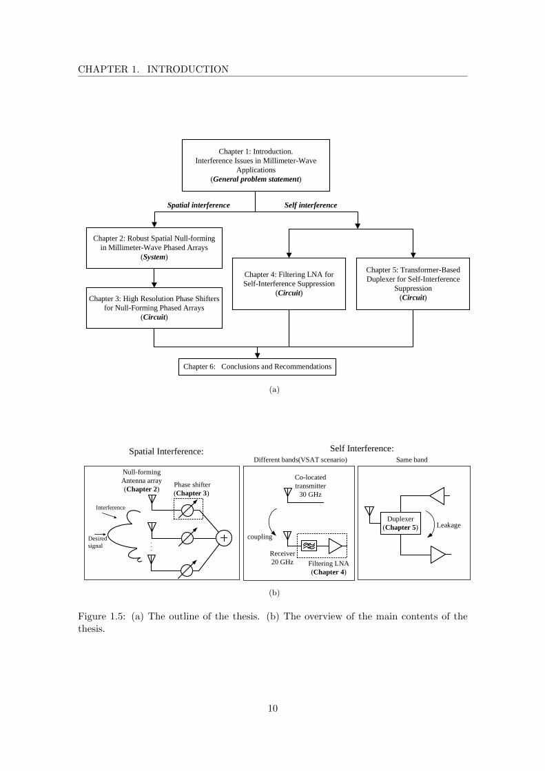
The outline and the overview of this thesis is shown in Fig. 1.5. Two main issues areinvestigated, i.e. spatial and self interference. In each chapter, the problems will beintroduced in more detail including literature reviews. The content of each chapter isbriefly explained below:
Chapter 2 and 3 focus on spatial interference issue in mm-wave applications:
• Chapter 2 proposes an analog/RF adaptive null-forming array for spatial interfer-ence mitigation, which is robust against practical impairments, such as phase andamplitude control errors and interference direction estimation errors.
• Chapter 3 investigates the design of high resolution phase shifters which are requiredfor the null-forming array proposed in the previous chapter. Two phase shifters areimplemented, i.e. an LO-path phase shifter and a Baseband phase shifter, both in40 nm CMOS technology.
Chapter 4 and 5 of the thesis investigate the self interference issue between the TXand RX. Two scenarios are investigated:
• In Chapter 4, the scenario investigated is a VSAT scenario, where the frequencies ofthe transmitter and receiver are at different bands. A filtering LNA is designed in0.25 µm SiGe BiCMOS which achieves a high attenuation at the TX frequency withminimal impact on the noise figure.
• Chapter 5 investigates a scenario where the TX and RX are in the same frequencyband. A hybrid-transformer based circular polarization duplexer is proposed andimplemented in 0.25 µm SiGe BiCMOS. The on-chip duplexer and a demonstratorwith on-board antennas demonstrate a high isolation of 50 dB between the TX andRX.
Chapter 6 provides the conclusions and the recommendations for future research.
9
CHAPTER 1. INTRODUCTION
Chapter 1: Introduction.Interference Issues in Millimeter-Wave
Applications(General problem statement)
Chapter 2: Robust Spatial Null-forming in Millimeter-Wave Phased Arrays
(System)
Chapter 3: High Resolution Phase Shifters for Null-Forming Phased Arrays
(Circuit)
Chapter 5: Transformer-Based Duplexer for Self-Interference
Suppression(Circuit)
Spatial interference Self interference
Chapter 6: Conclusions and Recommendations
Chapter 4: Filtering LNA for Self-Interference Suppression
(Circuit)
(a)
Spatial Interference:
Phase shifter (Chapter 3)
.
.
.
Null-formingAntenna array(Chapter 2)
Desiredsignal
Interference
Self Interference:Different bands(VSAT scenario) Same band
Co-located transmitter
30 GHz
Receiver20 GHz
coupling
Filtering LNA(Chapter 4)
LeakageDuplexer
(Chapter 5)
(b)
Figure 1.5: (a) The outline of the thesis. (b) The overview of the main contents of thethesis.
10

Chapter 2
Robust Spatial Null-forming inMillimeter-Wave Phased Arrays
2.1 Introduction
In recent years, the advances in silicon technologies have motivated extensive research andindustrial activities in wireless systems in the millimeter-wave frequency range (mm-wave,i.e. 30 - 300 GHz). At millimeter-wave frequencies, larger bandwidth is available and ithas the potential to support multi-Gbps data rates. One of the most popular bands isthe unlicensed 60 GHz band, and several standards are in development, e.g. the WirelessPersonal/Local Area Networks (WPAN [11], WLAN [12]). Due to the increasing interestsin this unlicensed band, we can foresee that in the future the band will become denselypopulated and devices of different standards are likely to co-exist. The co-channel inter-ference (CCI) will become an issue which can degrade the co-existence and the aggregatedata rates [26]. Frequency and time domain co-ordinations can be explored to mitigatethis interference problem. However, in the frequency domain, a maximum of only fournon-overlapping channels are specified in current standards. Besides, in the time domain,it is difficult to coordinate and synchronize between links of different standards.
A domain which offers opportunities for interference mitigation is the spatial domain.Phased arrays in recent 60 GHz systems [27] are mainly used to beam steering towards thedesired direction with extra array gain and to compensate the high path loss at 60 GHz.Actually, they simultaneously can be used to form nulls in other directions in order toattenuate interference. However, this is not fully exploited due to some practical impair-ments. Due to the power and cost constraints, the 60 GHz phased arrays typically tunethe weights (phase shifts and amplitudes) and then combine the signals in the analog/RFdomain, so that only one high speed analog-to-digital converter and base-band processingunit is required. The limited resolution and accuracy of the analog/RF weight control willlimit the control of the directions of the sharp nulls. Besides, it is challenging to estimatethe exact directions of interference in an analog/RF phased array. Due to these limitationsin practice, a robust method for better spatial selectivity is necessary for mm-wave phasedarrays.
11

CHAPTER 2. ROBUST SPATIAL NULL-FORMING
In this chapter, our goal is to find a robust and efficient method to maximize signal-to-interference-plus-noise ratio (SINR) for 60 GHz applications. We propose an adaptivereceiver array assisted by genetic algorithms (GA) [28] to mitigate the CCI in the spatialdomain. The algorithm adjusts the array pattern by manipulating the least-significant-bits(LSBs) of the weights to have a close-to-optimum SINR. Compared to other algorithms,e.g. gradient-based algorithms, GA is computationally efficient without being trapped inlocal maximas, and robust since precise knowledge of interferences is not required.
Two further improvements are proposed in order to improve spatial selectivity fordifferent situations. Firstly, we propose an algorithm that can automatically adapt thenumber of LSBs used by the GA to increase the SINR in different interference situations.For a dense 60 GHz indoor environment, the angle of arrival (AoA) of CCI can be closeto the AoA of the desired signal, in which case the optimization by standard GA cannot reach convergence with good SINR. The proposed adaptive GA can achieve a near-optimum SINR even when the AoA of the interferer is close to the AoA of the desiredsignal. Secondly, we incorporate antenna selection capabilities into the algorithm. Incase of line-of-sight situations and/or lower data rates, not all antennas are required tosatisfy the link budget, which leads to lower power consumption [27]. Compared to fixedselection, the extended GA which simultaneously performs antenna selection (out of thefull array) and weight optimization, provides larger interference suppression range andfurther improves the spatial selectivity.
The remainder of this chapter is organized as follows. Section 3.2 gives an introductionto the principle of uniform linear arrays, including the formulation of beam-steering andnull-forming. Section 3.3 discusses the impairments in practice that can degrade theperformance of the analog/RF null-forming arrays. To overcome the degradation due topractical impairments, an adaptive array with a genetic algorithm is proposed in section3.4. Section 3.5 presents simulation results on the proposed null-forming array. Section 3.6will discuss the implications in the practical implementation. The conclusions are givenin section 3.7.
2.2 Uniform Linear Array Principles
The first use of phased arrays dates back to the 1930’s [29] and has been developedthrough the decades in various applications, ranging from radar [30, 31], satellite [32] andcommunication [33, 12]. Despite the various applications of phased array systems, thebasic principle remains unchanged. In this section, the basic principle of uniform lineararrays is revisited, including the concept of beam-steering and null-forming.
2.2.1 Beam-Steering
We consider a uniform linear array (ULA) receiver consisting of N antennas, as shownin Fig. 2.1. The antennas are equally spaced with a distance d of half a wavelength,i.e. d = λ/2. In each path, there are independent weight controls on the phase (φk)and the amplitude (ak) of the signal. We assume 0 6 φk < 2π and 0 6 ak < 1. Thephase and amplitude controls, as indicated in the figure, can be implemented in practice
12

2.2. UNIFORM LINEAR ARRAY PRINCIPLES
Amplitude
.
.
.
.
.
.
1
k
N
θ
.
.
.
Output
sout(θ).
.
.
.
.
.
.
.
.
Phase
a1
ak
aN
ϕ1
ϕk
ϕN
Weight
Farfield signalsin(θ)
s1(θ)
sk(θ)
sN(θ)
Figure 2.1: General model of a phased array receiver.
respectively by a phase-shifter (PS) and a variable-gain-amplifier (VGA) 1. Throughoutthis chapter, we use phase shift rather than time delay because we consider here a relativelylow fractional bandwidth scenario. For a signal using a single channel (e.g. 2.16 GHz in[11, 12]) in the 60 GHz band, the fractional bandwidth is only about 3.6%, which onlyintroduces a main-lobe gain variation of less than 0.11 dB across the bandwidth for a16-path array with a ±60 main-lobe scanning range 2. Therefore, in this chapter, phaseshift approximation will be used instead of time delay.
We define the signal arriving at the first antenna (for k = 1) as A cos(2πf ·t), where A isthe amplitude of the received far field signal and f is the frequency of interest. We denote afarfield signal is incident from direction θ as sin(θ). This signal is received by each antennaat different time instances. Since the path length difference between adjacent antennasis d · sin(θ), the time delay difference between two adjacent antennas is ∆t(θ) = d·sin(θ)
c ,where c is the speed of light. So the signal at the kth antenna is:
sin,k(t, θ) = A · cos
(2πf · t− 2πf · (k − 1)d · sin(θ)
c
)= Re
A · ej·2πft · e−j·2πf ·
(k−1)d·sin(θ)c
(2.1)
The term A · ej·2πf ·t denotes the received farfield signal at the first antenna, and thesignal at each subsequent antenna sin,k has an extra phase difference dependent on θ.
After receiving the signal from each path, different weights can be applied to the signal,i.e. a phase shift of φk and an amplitude of ak in the kth path. The resulting signal in
1The absolute gain in each path is ignored in the model, and we normalize the ak to the maximumgain.
2The main-lobe gain variation is a function of the array size, scanning range and the fractional band-width. A detailed quantitative analysis is given in Appendix A.
13

CHAPTER 2. ROBUST SPATIAL NULL-FORMING
the kth path can then be represented as:
sk(t, θ) = ReA · ej·2πft · e−j·2πf ·
(k−1)d·sin(θ)c · ak · e−jφk
= Re
A · ej·2πft · ak · e
−j(
2πf · (k−1)d·sin(θ)c
+φk
) (2.2)
The final output after combining can then be derived as:
sout(t, θ) = Re
N∑k=1
sk(t, θ)
= Re
N∑k=1
A · ej·2πft · ak · e−j
(2πf · (k−1)d·sin(θ)
c+φk
)= Re
A · ej·2πft ·AF (θ)
(2.3)
where the AF (θ) is called the array factor, and:
AF (f, θ) =
N∑k=1
ak · e−j
(2πf · (k−1)d·sin(θ)
c+φk
)(2.4)
It denotes the array gain that can be achieved at θ. In case of a desired signal havingan angle-of-arrival (AoA) of θs, it is obvious that the maximum array gain at θs can beobtained if:
ak = 1
φk =
(−2πf · (k − 1)d · sin(θs)
c
)modulus of 2π
(2.5)
In other words, the complex weight in each path (the phase component) compensatesthe phase difference between the received signals that arrive at the various antennas, sothat the signals sk combine constructively at the output. In this case, AF (θs) at the desireddirection equals to N . This is also called beam-steering with constructive combining ofthe desired signal.
An example of the array factor of an 8-element phased array beam-steered to θ = 30
is shown in Fig. 2.2. As can be observed from the figure, the maximum AF, i.e. themain-lobe, is steered towards the desired AoA, thanks to the weight setting in each path.As a result of the beam-steering, the signal-to-noise ratio (SNR) of the receiver array willimprove by a factor of N . We assume an uncorrelated input referred noise power3 of A2
n,k
at the input of each path, with A2n,k = A2
n for k = 1, · · · , N . Since the noise in each pathis uncorrelated, it will combine in terms of power. When the desired signal is incident
3Here the input referred noise only includes the noise until the combining stage, since the noise afterthe combiner will not be weighted. To focus on the property of an antenna array, only the noise beforethe combiner is considered in the following analysis.
14

2.2. UNIFORM LINEAR ARRAY PRINCIPLES
−80 −60 −40 −20 0 20 40 60 80−15
−10
−5
0
5
10
15
20
25
θ (in degrees)
dB
Main−lobe
Side−lobe Null
Figure 2.2: Array factor of an 8-path phased array beam-steered to θs = 30 with half-wavelength spacing, i.e. d = λ/2 = c/2f .
with an AoA of θs, we can derive the SNR at the output of the array as:
SNRout =s2out(t, θs)∑Nk=1A
2n,k
= AF 2(θs) ·A2s∑N
k=1A2n,k
= N · A2s
A2n
(2.6)
which is N times better than a single-path’s SNR.
Thanks to beam-steering, the AF is focused towards a certain direction, while thegain for the other directions is lower. This provides some level of spatial interferencesuppression. In Fig. 2.2, we can also observe that there are side-lobes in directions otherthan the main-lobe; the highest side-lobe can have an absolute AF of about 5 dB. Thesesidelobes can still cause interference issues if a large interference happens to be aroundthe side-lobe directions. The side-lobes can be suppressed by amplitude tapering [34]instead of using a uniform amplitude where ak = 1 for k = 1, · · · , N . On the other hand,the amplitude will inevitably increase the main-lobe beam-width and reduce the gain.Amplitude tapering is more effective for large array sizes, and will not be explored in thiswork.
2.2.2 Null-Forming
In addition to the constructive combining in a specific direction, a phased array can alsogenerate spatial nulls in other directions, as shown in Fig. 2.2. In the presence of spatialinterferences, the weights in the phased array can be manipulated to adjust the directionsof the nulls to the interference directions. Actually, the theoretical optimum weight settingfor the signal-to-interference-plus-noise ratio (SINR) can be derived, given the knowledgeof interference power levels and directions. The derivation can be given from the signalprocessing perspective [35] as follows.
Eq. (2.3) can be re-written in vector form. The received signal from direction θs at
15

CHAPTER 2. ROBUST SPATIAL NULL-FORMING
−80 −60 −40 −20 0 20 40 60 80−25
−20
−15
−10
−5
0
5
10
15
20
θ (in degree)
dB
no optimizationwith w
max−SINRInterference 1 @−21
Interference 2 @38
Figure 2.3: The array patterns with a non-optimized weight and with the optimizedweight for SINR given by (2.13). In this example, the array has 8 element, and the powerof interferences are the same as the desired signal. The directions of the two interferencesare −21 and 38.
the output of the array can be written as:
sout,s(t) = ReAs · ej·2πft · vHs · w
(2.7)
where the subscript s denotes the desired signal, and vs and w are the desired signal’spropagation vector and the array’s weight vector, denoted as:
vHs = [1, · · · , e−j2πdλ
(k−1)·sin(θs), · · · , e−j2πdλ
(N−1)·sin(θs)] (2.8)
wH = [a1 · ejφ1 , · · · , ak · ejφk , · · · , aN · ejφN ] (2.9)
and the superscript H denotes the Hermitian operation which is the complex conjugateof the transpose of the marked matrix or vector.
We assume that there are Nint interferences, and they have amplitudes of Aint,l andAoA’s of θint,l for l = 1, · · · , Nint. Similar as Eq. (2.7), we can denote the l-th interferenceat the output sout,int,l(t) as:
sout,int,l(t) = ReAint,l · ej·2πft · vHint,l · w
(2.10)
where:vHint,l = [1, · · · , e−j
2πdλ
(N−1)·sin(θint,l)] (2.11)
The output SINRout can then be written as:
SINRout =|sout,s(t)|2∑Nint
l=1 |sout,int,l(t)|2 +∑N
k=1A2n,k
=wH
(A2s · vsvHs
)w
wH[∑Ni
l=1
(A2int,l · vint,l · vHint,l
)+A2
n · IN]w
(2.12)
with the assumption that the receiver array has no knowledge on the interferences andexperiences them as noise. IN is an identity matrix of size N . If the powers (A2
s and
16

2.3. PRACTICAL DEGRADATIONS TO ANALOG/RF NULL-FORMING ARRAYS
A2int,l) and AoA’s (θs and θint,l) of the desired signal and interferences are known, it is
known that the solution for maximum SINR can be derived as follows [35]:
wmax−SINR = βc ·A2s
[A2n · IN +
Ni∑l=1
(A2int,l · vint,l · vHint,l
)]−1
· vs (2.13)
where βc is a normalization constant. This max-SINR solution gives the maximum achiev-able SINR in theory. Fig. 2.3 shows an example of the optimized array factor of an 8-element phased array in presence of a desired signal at 0 and two interferences at −21
and 38. The interferences have the same power level as the desired signal in this ex-ample. For the reference array factor, we can see that the interferences are entering thetwo side-lobes. With the theoretical optimum weight wmax−SINR, two spatial nulls aretuned to the interference directions, and the SINR is improved from 10.4 dB using thenon-optimized weights to 17.8 dB, i.e. an improvement of 7.4 dB.
2.3 Practical Degradations to Analog/RF Null-Forming Ar-rays
In the last section, principles of beam-steering and null-forming of a ULA are revisited,and the closed-form solution for the optimum SINR in the presence of a spatial interfer-ence is introduced. Continuous phase shifts and amplitude controls are assumed in thewmax−SINR in Fig. 2.3, and knowledge of precise interference directions and power lev-els is assumed as well. However, due to the practical impairments, the performance of anull-forming phased array might be degraded. Particularly, the spatial nulls in the arraypattern are sharp and sensitive in angle. For example, as can be observed from Fig. 2.3,a minor shift of the null at −20 can significantly degrade the attenuation.
In this section, we will focus on several main impairments in an analog/RF phasedarray, including the quantization on the weights, the inaccuracy on the weights and theestimation error on the interference direction. We will demonstrate the sensitivity of thenull-forming due to these impairments through simulations.
Quantized weights
Discrete phase shifters and variable gain amplifiers [36, 37, 38] are typically used in practi-cal systems4. The first source of the impairments is the quantization error in the weights,both for their phase shifts and amplitudes. We demonstrate the effect of quantized phaseshift and amplitude values on wmax−SINR with different number of bits, using Fig. 2.4.In the simulation, a ULA consisting of 8 elements is assumed and it is beam-steered to θs= 0 for a desired signal. A single element has an SNR of 9 dB in case of no interference,which means the total SNR from an 8-element array is 18 dB. An interference is assumedwith a 10 dB higher power level than the desired signal, while its AoA (θint) is swept from5 to 85. For each AoA of the interference, wmax−SINR is calculated using (2.13), and the
4Continuous phase shifters can also be implemented [33, 39]; they will require digital-to-analog convert-ers for the control signals from the base-band.
17

CHAPTER 2. ROBUST SPATIAL NULL-FORMING
corresponding SINR is plotted in Fig. 2.4 as dashed lines. The SINR with no optimizationis also calculate with ak = 1 and φk = 0 for each path for k = 1, · · · , N (which simplybeam-steers the pattern towards θs = 0), as shown in Fig. 2.4 as dashed-dotted lines. Ascan be expected, the SINR values are significantly improved to around 18 dB except for|θint| less then 10 in which case the interference is too close to the desired signal and themain-lobe gain has to be influenced by the wmax−SINR in order to place a null close tothe main-lobe.
However, the quantization on wmax−SINR can degrade the SINR. Different numbersof bits are applied to quantize the phase and amplitude of wmax−SINR, i.e. Nbit,ps andNbit,amp. In the simulation, the phase shifts and amplitudes of wmax−SINR are roundedto the closest uniformly quantized steps, which are:
φqtz,n =(n− 1) · 2π2Nbit,ps − 1
, for n = 1, · · · , 2Nbit,ps
aqtz,m =m− 1
2Nbit,amp − 1, for m = 1, · · · , 2Nbit,amp
(2.14)
The quantized weights are applied to (2.12) to calculate the resulting SINR. Whenusing 4-bit phase shifters with continuous ideal amplitudes, as shown in Fig. 2.4(a), theSINR can drop to below 10 dB, while minimal influence on the SINR can be obtainedonly when the phase quantization is at least 6-bit. In case of quantized amplitudes withcontinuous phase shifts, as shown in Fig. 2.4(b), the influence on the SINR is less sensitive,and a 3-bit amplitude quantization already gives minimal impact. With both the phase andamplitude quantization, as shown in Fig. 2.4(c), minimal impact on the SINR is obtainedwhen Nbit,ps = 6 and Nbit,amp = 4, with ideal quantized steps. Similar conclusions applyto a 16-element ULA, as shown in Fig. 2.5.
Error in the weights
On top of the quantization effect, errors can further degrade the null-forming performanceeven with a high number of bits. First, the discrete steps from the quantization can beinaccurate, which can be due to the limited accuracy of the analog/RF phase shiftersand variable gain amplifiers, especially when operating in the range of millimeter-wavefrequencies. Second, there can be path-to-path mismatches. The adjacent paths areseparated on-chip, and due to process variation, the exact phase shift and amplitude forthe same bit setting in each path can be different. Besides, the path-to-path mismatchcan also come from the antennas and its interface to the chip (if off-chip antennas areused). Third, other causes such as temperature and supply variations can also introducetime-varying variations.
The impact of the random errors on the SINR of the null-forming array will be simu-lated next. We can model the quantization inaccuracy and the path-to-path mismatch bya random error on each quantized step and an offset error on all the settings in each path,respectively. We define all the random errors with a Gaussian distribution which has amean value of zero, and respective standard deviations of:
18

2.3. PRACTICAL DEGRADATIONS TO ANALOG/RF NULL-FORMING ARRAYS
0 10 20 30 40 50 60 70 80 90−5
0
5
10
15
20SINR when N = 8, θs = 0
θint
(in degree)
dB
optimum with wmax−SINR
no optimizationNbit,ps = 4Nbit,ps = 5Nbit,ps = 6
(a)
0 10 20 30 40 50 60 70 80 90−5
0
5
10
15
20SINR when N = 8, θs = 0
θint
(in degree)
dB
optimum with wmax−SINR
no optimizationNbit,amp = 2Nbit,amp = 3Nbit,amp = 4
(b)
0 10 20 30 40 50 60 70 80 90−5
0
5
10
15
20SINR when N = 8, θs = 0
θint
(in degree)
dB
optimum with wmax−SINR
no optimizationNbit,ps = 4, Nbit,amp = 2Nbit,ps = 5, Nbit,amp = 3Nbit,ps = 6, Nbit,amp = 4
(c)
Figure 2.4: The SINR values versus the interference direction on an 8-element ULA usingdifferent weights: a non-optimized weight for beam-steering only, an ideal optimized weightvector from (2.13), and optimized weight after quantization with different number of bitson phase shift and/or amplitude. (a) with quantized phase shift, (b) with quantizedamplitude, (c) with quantized phase shift and amplitude.
19

CHAPTER 2. ROBUST SPATIAL NULL-FORMING
0 10 20 30 40 50 60 70 80 90−5
0
5
10
15
20
25SINR when N = 16, θs = 0
θint
(in degree)
dB
optimum with wmax−SINR
no optimizationNbit,ps = 4Nbit,ps = 5Nbit,ps = 6
(a)
0 10 20 30 40 50 60 70 80 90−5
0
5
10
15
20
25SINR when N = 16, θs = 0
θint
(in degree)
dB
optimum with wmax−SINR
no optimizationNbit,amp = 2Nbit,amp = 3Nbit,amp = 4
(b)
0 10 20 30 40 50 60 70 80 90−5
0
5
10
15
20
25SINR when N = 16, θs = 0
θint
(in degree)
dB
optimum with wmax−SINR
no optimizationNbit,ps = 4, Nbit,amp = 2Nbit,ps = 5, Nbit,amp = 3Nbit,ps = 6, Nbit,amp = 4
(c)
Figure 2.5: The SINR values versus the interference direction on a 16-element ULA usingdifferent weights: a non-optimized weight for beam-steering only, an ideal optimized weightvector from (2.13), and optimized weight after quantization with different number of bitson phase shift and/or amplitude. (a) with quantized phase shift, (b) with quantizedamplitude, (c) with quantized phase shift and amplitude.
20

2.3. PRACTICAL DEGRADATIONS TO ANALOG/RF NULL-FORMING ARRAYS
0 10 20 30 40 50 60 70 80 90−5
0
5
10
15
20SINR when N = 8, θs = 0
θint
(in degree)
dB
optimum with wmax−SINR
no optimizationNbit,ps = 6, Nbit,amp = 4Nbit,ps = 6, Nbit,amp = 4, with random errors
Figure 2.6: The SINR using wmax−SINR optimized for different AoA of interference withrandom errors, including errors on the quantized steps and offset error between paths.The errors are generated independently 1000 times. The average value and the range areplotted for each θint. Also plotted are the ideal SINR, reference SINR and the SINR withideally quantized wmax−SINR for comparison.
Phase shift quantization steps : σps,qtz=20%×(Phase shift resolution)Amplitude quantization steps : σamp,qtz=20%×(Amplitude resolution)Offset on all the phase shift steps in each path : σps,offset=4
Offset on all the amplitude steps in each path : σamp,offset=5%
In order to demonstrate the sensitivity to the errors, the above assumed errors arerealistic and even relatively low. For example, the phase offset between paths can easilyexceed 4 without dedicated calibration, considering the process spread, on-chip coupling,and antenna mismatch. With these four random errors included in the quantized optimumweight wmax−SINR, we can evaluate the SINR similar as in Fig. 2.4. The four error itemsare generated independently 1000 times and applied to wmax−SINR derived for differentdirections of the interference, which has has a 10 dB higher power level than the powerof the desired signal. The average value, minimum and maximum values of the resultingSINR are plotted in Fig. 2.6. We can observe that the average SINR’s are degraded byabout 2 dB, and in the worst cases, the SINR’s are degraded to below 10 dB.
The errors in the weights can be characterized and corrected through dedicated cali-bration and/or built-in-self-test hardware. However, it will inevitably increase complexity,since it is necessary to determine the error in each setting.
Direction estimation error
Other than the quantization or random errors on the weight control, the exact directionof the interference is difficult to obtain in practice for an analog/RF array. For digitaladaptive arrays, there are dedicated algorithms that can estimate the AoA [40]. But for
21
CHAPTER 2. ROBUST SPATIAL NULL-FORMING
0 10 20 30 40 50 60 70 80 90−5
0
5
10
15
20SINR when N = 8, θs = 0
θint
(in degree)
dB
optimum with wmax−SINR
no optimization
Nbit,ps = 6, Nbit,amp = 4
Nbit,ps = 6, Nbit,amp = 4
with interference estimation errors
Figure 2.7: The SINR using w′max−SINR optimized for different AoA of interference with
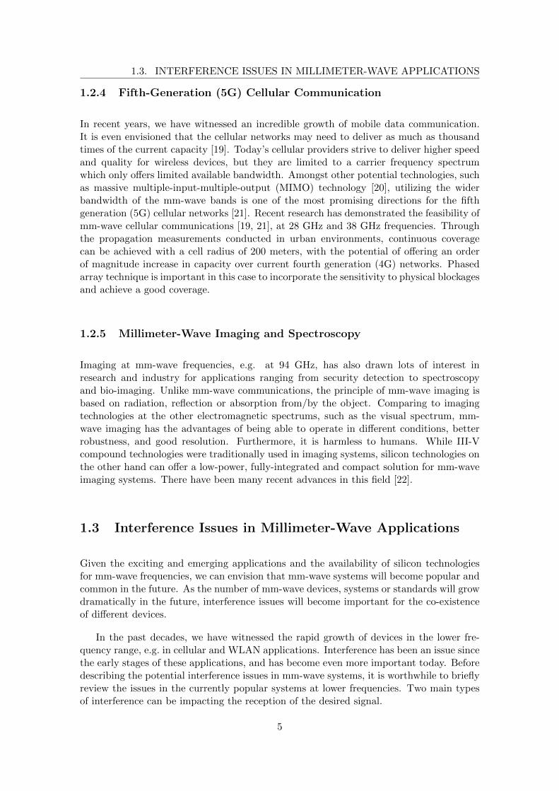
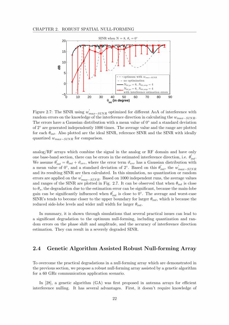
random errors on the knowledge of the interference direction in calculating the wmax−SINR.The errors have a Gaussian distribution with a mean value of 0 and a standard deviationof 2 are generated independently 1000 times. The average value and the range are plottedfor each θint. Also plotted are the ideal SINR, reference SINR and the SINR with ideallyquantized wmax−SINR for comparison.
analog/RF arrays which combine the signal in the analog or RF domain and have onlyone base-band section, there can be errors in the estimated interference direction, i.e. θ
′int.
We assume θ′int = θint + ϑerr, where the error term ϑerr has a Gaussian distribution with
a mean value of 0, and a standard deviation of 2. Based on this θ′int, the w
′max−SINR
and its resulting SINR are then calculated. In this simulation, no quantization or randomerrors are applied on the w
′max−SINR. Based on 1000 independent runs, the average values
and ranges of the SINR are plotted in Fig. 2.7. It can be observed that when θint is closeto θs, the degradation due to the estimation error can be significant, because the main-lobegain can be significantly influenced when θ
′int is close to 0. The average and worst-case
SINR’s tends to become closer to the upper boundary for larger θint, which is because thereduced side-lobe levels and wider null width for larger θint.
In summary, it is shown through simulations that several practical issues can lead toa significant degradation to the optimum null-forming, including quantization and ran-dom errors on the phase shift and amplitude, and the accuracy of interference directionestimation. They can result in a severely degraded SINR.
2.4 Genetic Algorithm Assisted Robust Null-forming Array
To overcome the practical degradations in a null-forming array which are demonstrated inthe previous section, we propose a robust null-forming array assisted by a genetic algorithmfor a 60 GHz communication application scenario.
In [28], a genetic algorithm (GA) was first proposed in antenna arrays for efficientinterference nulling. It has several advantages. First, it doesn’t require knowledge of
22

2.4. GENETIC ALGORITHM ASSISTED ROBUST NULL-FORMING ARRAY
Genetic
Algorithm
Core
Phase shifter
MSBs LSBs
Variable-Gain-
Amplifier
.
.
.
.
.
.
.
.
.
Antenna
Power
Detector
1
k
Ntot
θs
θ i.l
desired signal
l-th
interference
.
.
.
Output
.
.
.
.
.
.
.
.
.
.
.
.
sp=k
Figure 2.8: Adaptive null-forming array assisted by a Genetic Algorithm. The phaseshifters have in total Nbit,ps-bit and the VGAs have Nbit,vga-bit. The MSBs are used formainlobe control, while the LSBs are manipulated by a genetic algorithm to adjust thenulls. The number of the LSBs and MSBs can be adjusted in case when nulls are closeto the desired signal. Furthermore, the array has antenna selection capability and theoptimum selection of active antennas can be jointly optimized by the genetic algorithm.
the interference directions and power levels. Second, it has a fast convergence speed andtherefore it is potentially suitable for low-latency applications, e.g. wireless HD stream-ing. Third, it requires only one ADC and baseband processor which are relatively powerconsuming for multi-Gigabits processing. Therefore, we propose an adaptive array withGA to mitigate spatial co-channel interference for 60 GHz applications. The robustnessagainst practical impairments will be verified. Furthermore, we will improve the methodto be able to null nearby interference and to include antenna selection capabilities.
2.4.1 Proposed Method
Fig. 2.8 shows the proposed array architecture. It adopts Nbit,ps-bit phase-shifters andNbit,vga-bit variable-gain-amplifiers (VGA). In each path, the most-significant-bits (MSBs)of the phase-shifter (Nbit,ps,MSB) are dedicated to control the main-lobe, while the least-significant-bits (LSBs) of the phase-shifters (Nbit,ps,LSB) and the VGAs (Nbit,vga,LSB) aremanipulated by an optimization algorithm to add perturbation in the array pattern toadjust the nulls at interference directions. With the MSBs fixed for steering the main-lobe to the desired direction, the LSBs can be adjusted without changing the mani-lobesignificantly. The LSBs can significantly influence the directions of the nulls to suppressthe interferers.
23

CHAPTER 2. ROBUST SPATIAL NULL-FORMING
In case of fixed MSBs, the main-lobe direction is relatively fixed. In order to maximizethe SINR, we can reduce the power of the undesired signals, i.e. the denominator inequation (2.12). As a result, before the desired signal reception, we can allocate a timeslot for minimizing the power of the undesired signals. The power at the output canbe measured, as shown in Fig. 2.8, and the information is fed to the algorithm corewhich will gradually optimize the LSB settings to reduce the total received power. Thepower detector block in the figure can re-use the received-signal-strength-indicator (RSSI)function necessary in the standards [11, 12].
The procedure can be as follows. It starts a by beacon communication, after whichthe direction of the desired signal is decided at the RX side, determining the MSBs of thephase-shifters. This can be implemented using the beamforming protocols in the available60 GHz standards [11]. After the beacon communication and before starting the datacommunication, a dedicated time slot is allocated to apply optimization on the phase andamplitude LSBs settings to minimize the reception of undesired signal at the output, alsodenoted as the denominator in (2.12). When the algorithm converges, which means theundesired signal power is minimized, an acknowledgement is sent to the TX side to startthe desired signal transmission and the communication starts.
Actually, we can extend the method further with other forms of signal quality detectors.For example, instead of using a power detection as in Fig. 2.8, bit-error-rate (BER)detection in the base-band is an alternative. In this work, we will only focus on thesolution using a power detector to demonstrate the improvement on the spatial selectivity,keeping in mind other possibilities.
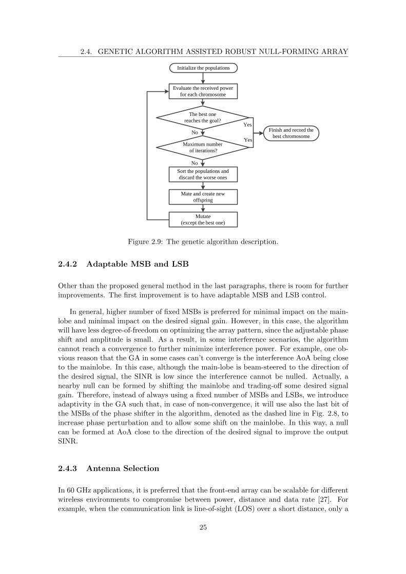
As said, regarding the optimization, a genetic algorithm is proposed for the algorithmcore due to its fast convergence speed and its search for global optimum [28, 41, 42]. Beingan evolutionary algorithm, the GA used in this work iteratively optimizes the weightingLSBs to reduce the output interference power until the algorithm reaches a convergencethreshold on the minimum allowed interference power level. The GA used in this workconsists of typical GA operations, as shown in Fig. 2.9. One set of the LSBs from theweights in all paths is coded as a single string of bits, which is called a chromosome inthe algorithm. The operations in the GA include random generation of a populationof chromosomes, chromosome evaluation, selection with elitism based on roulette wheelweighting, uniform crossover and mutation [43]. In general, only better performing chro-mosomes will survive and will be used to generate the new chromosomes, which ensuresthe tendency of evolution towards better results. The mutation operation creates thepossibility to explore the whole search space, without ending in a local-optimum. Thedetailed description of all the operations are presented in Appendix B. The main goal is tominimize the number of iterations to reach convergence. The parameters in the algorithmare critical for the convergence speed, and need careful selection. The detailed derivationof the parameters in the GA in this work is also presented in Appendix B. The conclusionfrom Appendix B suggests that a population size of 4, with mutation rate and discardrate of 7% and 50% respectively gives good convergence performance.
24
2.4. GENETIC ALGORITHM ASSISTED ROBUST NULL-FORMING ARRAY
The best one reaches the goal?
Evaluate the received power for each chromosome
Sort the populations and discard the worse ones
Mate and create new offspring
No
Maximum number of iterations?
No
Initialize the populations
Finish and record the best chromosome
Yes
Yes
Mutate(except the best one)
Figure 2.9: The genetic algorithm description.
2.4.2 Adaptable MSB and LSB
Other than the proposed general method in the last paragraphs, there is room for furtherimprovements. The first improvement is to have adaptable MSB and LSB control.
In general, higher number of fixed MSBs is preferred for minimal impact on the main-lobe and minimal impact on the desired signal gain. However, in this case, the algorithmwill have less degree-of-freedom on optimizing the array pattern, since the adjustable phaseshift and amplitude is small. As a result, in some interference scenarios, the algorithmcannot reach a convergence to further minimize interference power. For example, one ob-vious reason that the GA in some cases can’t converge is the interference AoA being closeto the mainlobe. In this case, although the main-lobe is beam-steered to the direction ofthe desired signal, the SINR is low since the interference cannot be nulled. Actually, anearby null can be formed by shifting the mainlobe and trading-off some desired signalgain. Therefore, instead of always using a fixed number of MSBs and LSBs, we introduceadaptivity in the GA such that, in case of non-convergence, it will use also the last bit ofthe MSBs of the phase shifter in the algorithm, denoted as the dashed line in Fig. 2.8, toincrease phase perturbation and to allow some shift on the mainlobe. In this way, a nullcan be formed at AoA close to the direction of the desired signal to improve the outputSINR.
2.4.3 Antenna Selection
In 60 GHz applications, it is preferred that the front-end array can be scalable for differentwireless environments to compromise between power, distance and data rate [27]. Forexample, when the communication link is line-of-sight (LOS) over a short distance, only a
25

CHAPTER 2. ROBUST SPATIAL NULL-FORMING
fraction of the antennas is needed to achieve a certain link budget, while the full array willbe used for larger distances and/or non-line-of-sight (NLOS) situations. When less thanthe total available antennas are required, we propose to carry out the antenna selection inthe GA to increase diversity. Compared to a fixed ULA with λ/2 spacings, a linear arraywith larger spacings can form more nulls in the array pattern and the beam-width of themainlobe can be narrower. This can actually improve the interference nulling capability.To implement this in the GA, we extend the chromosomes with selection bits. Here, anexample is given on a ULA of a total size of eight elements (N = 8) and only four antennasare needed (Nsel = 4). In this case, an example of a single extended chromosome withantenna selection is shown below:
Antenna selection bits: 0 1 1 0 0 1 1 0
Weighting bits: 001 010 010 001
For the weighting bits, the four groups each with 3 bits correspond to the LSBs ofthe weights in the four selected antenna paths. The position of the selected antennasare denoted as 1 in the selection bits. When crossover and mutation are done on theselection bits, we constrain the number of 1s to Nsel. The GA treats the selection bitsand weighting bits as one chromosome, so to jointly optimize them in order to minimizethe received undesired power.
2.4.4 The Summary of the Combined Method
As a summary of the proposed method, the adaptive null-forming array adjusts the LSBsof the phase shifters and variable gain amplifiers to reduce the output interference powerwhich effectively creates nulls towards the interference directions. Further extensionsby adding adaptivity in the MSB and LSB control and antenna selection capability canimprove the null-forming performance in different situations. There are three main ad-vantages of this method:
1. Knowledge of the directions of the interferences is not critical. It is only importantto know the direction of the desired signal to set the MSBs, and it doesn’t have to beaccurate, because of the relatively wide beamwidth of the mainlobe. After this, theGA will evaluate and minimize the output undesired power, without the necessity ofknowing the direction of the interference. This avoids the accurate AoA estimationas required for the closed-form derivation for the wmax−SINR in (2.13).
2. This method is efficient in finding a close-to-optimum solution. The GA doesn’t re-quire much computation complexity, and the convergence speed is fast, as suggestedin [44, 28]. This will also be verified in the next section by simulations.
3. The GA is robust to weight errors. The actual phase-shift and amplitude can haveerrors around the quantized levels especially in the analog/RF implementation. Butthe GA can automatically search for better settings to compensate the errors. As aresult, accurate calibrations are not needed in this method.
26

2.5. SIMULATION RESULTS
In order to evaluate the performance of the proposed method, simulation results willbe presented in the next section.
2.5 Simulation Results
The following simulations are done on a ULA with d = λ/2 spacing between adjacentantennas. We use Nbit,ps,MSB = 4, Nbit,ps,LSB = 2, Nbit,amp,MSB = 2, Nbit,amp,LSB = 1considering both the implementation complexity and convergence in the algorithm. Themotivation of these numbers of bits will be explained in Section 2.6, while here we willdirectly apply these values to demonstrate the performance of the proposed method. Forthe desired signal, we consider only the LOS channel between the intended TX and RX,and assume θs = 0 and A2
s = −64 dBm. The noise figure (NF) of a single path (until thecombiner) is assumed to be 8 dB, so A2
n = −73 dBm for 2 GHz signal bandwidth5. TheGA core uses a small population size of 4 and a mutation rate of 0.07, which are chosenfor higher convergence speed, as discussed in Appendix B.
2.5.1 Array Pattern Simulations
First, the array patterns are simulated assuming certain interference AoAs. Three arraypatterns will be compared for each case:
1. Reference array pattern. It only points the mainlobe to the broadside, i.e. thedirection of the desired signal, without any adaptivity, i.e. ak = 1 and φk = 0 fork = 1, · · · , N .
2. Optimized array pattern using wmax−SINR. It assumes precise knowledge of theAoA(s) and power level(s) of the interference(s) in (2.13).
3. GA optimized array pattern. The settings are specified in the last subsection. TheGA function call ends when the undesired signal power (i.e. the denominator in(2.12)) is below a threshold level, which is here defined to be ∆u (in dB) higher thanthe noise floor. This ∆u, being the allowance for interference, is set to be 0.3 dBhere, in order to ensure a convergence meanwhile having enough suppression on theinterference.
To demonstrate the optimized array pattern, we simulate a 16-element ULA. The firstcase assumes two interferences of power -60 dBm with angles of θi,1 = −10 and θi,2 = 26
respectively, indicated by the arrows in Fig. 2.10(a). The optimization uses all the 16paths without antenna selection. For the reference array pattern, the two interferencesare entering the side-lobes, which leads to an SINR of only 8.25 dB. The pattern by themax-SINR solution forms deep nulls at the interference directions, and gives an SINRof 20.85 dB. The solid line which is optimized by the GA achieves a close-to-optimum
5The noise floor A2n is calculated as A2
n = −174dBm/Hz +NF + 10 log(BW ), where BW is the signalbandwidth in Hz.
27

CHAPTER 2. ROBUST SPATIAL NULL-FORMING
−80 −60 −40 −20 0 20 40 60 80
−20
−10
0
10
20
θ (in degree)
dB
Referencewmax−SINR optimizedGA optimized
(a)
0 10 20 30 40 50 608
10
12
14
16
18
20
22
Number of iterations
dB
(b)
Figure 2.10: (a) The array patterns on a 16-element ULA assuming two interferences withAoAs of θi,1 = −10 and θi,2 = 26 (denoted as arrows in the figure); (b) The optimizationby the GA on the SINR versus iterations.
28

2.5. SIMULATION RESULTS
Table 2.1: SINRs by different optimizations for small AoAs of an interference
AoASINR (dB)
with adapted (Nbit, ps, MSB, Nbit, ps, LSB)
SINR (dB)with fixed
(Nbit, ps, MSB=4, Nbit, ps, LSB=2)
max-SINR(dB)
6°20.4 to 20.9
(4, 2)20.4 to 20.9 21
5°19.1 to 20.2
(3, 3)12.3 to 19.8 20.5
4°18.7 to 19.2
(3, 3)5.1 to 7.3 19.5
3°11.7 to 16.6
(2, 4)0.69 to 1.24 17.7
Table 2.2: The GA optimized antenna selection and the weights.
1 3 4 6 11 13 14 161 1 1 0.875 0.875 1 1 10 11.25 5.625 5.625 -5.625 -5.625 -11.25 0Phase Shift(°):
Selected Elements:Amplitude:
output SINR of 20.62 dB. For this specific GA run, the optimization converges at the58-th iteration, as shown in 2.10(b). This is a small number of iteration to meet a close-to-optimum result, considering the size of the search space. The length of the chromosomein the GA is 48 bits (3 LSBs in each of the 16 paths), which corresponds to a search spaceof 248 possibilities. Furthermore, as can be observed in Fig. 2.10(b), at the 12-th iteration,the SINR is already significantly improved to more than 18 dB.
Next, we consider a situation when the interference is within the main-lobe direction.We assume an interference with θi = 4. In this case, Nbit,ps,LSB = 2 in the GA cannotreach the convergence threshold. Instead, Nbit,ps,LSB = 3 is necessary. The referencearray pattern gives an output SINR of only 1.02 dB. The max-SINR solution improvesthe SINR to 19.46 dB and the GA converges to a near-optimum SINR of 19.09 dB within68 iterations, as shown in Fig. 2.11. In this case, the size of the search space is 264, sinceone more LSB from each path is involved in the optimization.
Table. 2.1 shows the optimized SINRs for small interference AoAs, recorded from 100independent simulation runs for each AoA. The GA with adaptive weight control can givenear-optimum SINR for very small interference AoAs, up to 4, while the GA with fixedweight control degrades significantly for small AoAs. For even smaller angles, e.g. 3, whileoutperforming the SINRs by fixed weight control in average, the SINRs by the adaptiveGA suffers from variations due to the large perturbation imposed on the mainlobe.
The performance of the GA with antenna selection is shown in Fig. 2.12. Supposea link budget requires only 8 receiver paths out of a 16-element ULA. We assume two−60 dBm interferences with θi,1 = −6 and θi,1 = 21. When adopting a ULA of size 8with λ/2 spacing, the interferences are entering the mainlobe and sidelobe of the referencearray pattern, and the SINR is -1.76 dB. The reference pattern is not shown in the figurefor better clarity. Max-SINR solution on this ULA improves the SINR to 14.21 dB.
29

CHAPTER 2. ROBUST SPATIAL NULL-FORMING
−80 −60 −40 −20 0 20 40 60 80
−20
−10
0
10
20
θ (in degree)
dB
Referencewmax−SINR optimizedGA optimized
(a)
0 10 20 30 40 50 60 700
5
10
15
20
Number of iterations
dB
(b)
Figure 2.11: (a) The array patterns on a 16-element ULA assuming one interferenceentering the main-lobe with AoAs of θi,1 = 4 (denoted as arrow in the figure); (b) Theoptimization by the GA on the SINR versus iterations.
30

2.5. SIMULATION RESULTS
−80 −60 −40 −20 0 20 40 60 80
−30
−20
−10
0
10
20
θ (in degree)
dB
wmax−SINR optimized, N = 8
GA optimized, N = 8, no selection
GA optimized, N = 16, Nsel = 8
(a)
0 2 4 6 8 10 12 14 16 185
10
15
20
Number of iterations
dB
GA optimized, N = 16, Nsel = 8GA optimized, N = 8, no selection
(b)
Figure 2.12: (a) The array patterns on a 8-element ULA and a ULA of 16 elements intotal which has the antenna selection of 8 working antennas. The interference directionsare assumed to be θi,1 = 6 and θi,2 = 21 (denoted as arrow in the figure); (b) Theoptimization by the GA on the SINR versus iterations.
31

CHAPTER 2. ROBUST SPATIAL NULL-FORMING
The GA optimization on a 8-element ULA gives a relatively close value, 12.99 dB. Thecorresponding array pattern is shown as dotted line in Fig. 2.12(a). The GA with selectioncapability can give an even better performance. Denoted as solid line in Fig. 2.12(a), thearray pattern with antenna selection has a smaller main-lobe beamwidth, so a null can begenerated at small AoAs without shifting the mainlobe which is the case for the 8-elementULA. Its SINR is 17.95 dB which is 3.74 dB higher than the theoretical max-SINR solutionon the 8-element ULA. Notice also that more nulls are generated in the pattern, which inprinciple gives more degrees-of-freedom in interference nulling. The reason of the narrowermain-lobe beamwidth and the higher number of nulls is the larger average spacing betweenadjacent selected antennas. The side-effect of it is the increased side-lobe levels, as shownalso in Fig. 2.12(a). However, the algorithm makes sure that the side-lobes will not beat the interference directions. The selected antenna positions and their correspondingweights for the optimized array pattern are listed in Tab.2.2.
2.5.2 Statistical SINR Simulations for an Indoor Scenario
In the last sub-sections, simulations are done for certain directions of interferences. Thechosen directions are some relatively worse cases (e.g. interferences coming from the side-lobe directions) to demonstrate the improvement by the proposed method. It is alsointeresting to verify the improvement on the spatial selectivity by a statistical simulationwhich assumes random directions of interferences.
In the following paragraphs, in order to evaluate the spatial re-use gain of the GAassisted array, statistical simulations based on a simplified indoor environment are con-ducted [26]. The top view of a room of size 10 m × 10 m is assumed, as shown in Fig.2.13. The receiver array is located at the center of the room’s sidewall, and the desiredtransmitter is located on the other side of the room with a distance of 10 meters. Inaddition, an interference transmitter and a reflector are randomly placed in the room. Weassume the interference transmitter has a ULA of 8 antennas, each transmitting 6 dBm onthe same frequency channel as the intended TX. The array pattern of the interference TXhas a random main-lobe direction without any null-forming. This results in two potentialinterfering signals reaching the desired receiver by a direct and in-direct reflected pathvia the reflector, the power levels of which depend on the path lengths. The reflectionloss is assumed to be 4 dB. Here we assume that the direct signal and the reflected signalare uncorrelated, because the delay between two signals is typically much larger than thesymbol duration of a 2 GHz bandwidth signal.
In the statistical simulations, the interference and reflector placement and direction ofthe interference’s array pattern are randomly generated 104 times. The initial setting ofthe GA uses Nbit,ps,LSB = 2 and Nbit,amp,LSB = 1 as in the last sub-sections. In case ofnon-convergence, the GA increases the number of phase-shifter LSBs until a maximum of4.
For the 104 independent runs, the complementary cumulative distribution functions(CCDF)6 of the SINR are compared, as shown in Fig. 2.14. In the figure, results on ULAs
6The CCDF describes the probability of the SINR being higher than or equal to a certain value (in thex-axis).
32

2.5. SIMULATION RESULTS
Intended TX
Interference TX Reflector
Intended RX
10 meters
10 meters
Figure 2.13: Indoor environment simulation setup.
with 4, 8 or 16 working paths are shown. First we examine the fixed ULA of size 16 withoutantenna selection. When using the reference pattern, the SINR degrades to around 10 dBfrom 21 dB for 90% level indicated by the solid line, which means that for 10% of the casesthe SINR is below 10 dB. This implies a potential CCI problem: even though a phasedarray is used, CCI can still degrade the SINR, e.g. by entering the side-lobes or close tothe main-lobe. The optimum by wmax−SINR with perfect knowledge of the interferencesimproved the SINR at 90% level to 18.4 dB, as shown by the solid-diamond line. For theproposed GA assisted adaptive array, its CCDF on a ULA of size 16 is close to the idealmax-SINR optimization, indicated by the solid-square line. The SINR is 17 dB at the90% probability level, which means a 7 dB spatial re-use gain. The maximum SINR thatit can achieve in most cases is slightly below the highest value which is 21 dB, because ofthe perturbation on the mainlobe when the interference is not severe. But this trade-off(less than 0.5 dB) is minor compared to the performance improvement when interferencestarts to have a significant impact.
Similar improvements can be observed also for the results by ULAs with 4 or 8 work-ing paths, and the CCDF of the GA optimized array is close to the one optimized bywmax−SINR and improved significantly from the reference array without any optimiza-tion. Notice also that larger array size can better sustain the highest SINR and providea more stable SINR improvement (in other words, a more vertical curve around the highSINR part). This is because the larger array has higher directivity and is capable ofgenerating more spatial nulls in the array pattern.
In Fig. 2.14, the performance improvement by adding antenna selection is also shownby the dashed and dashed-symbolic lines. In cases where 8 antenna paths are used, thefixed ULA with λ/2 spacings already achieved a spatial re-use gain by applying the GAwithout selection. However, including the antenna selection capability in the GA gives aneven better result than the max-SINR solution, thanks to its capability to null CCI withsmall AoAs and more degrees-of-freedom in nulling. This was also observed previouslyin Fig. 2.12. With antenna selection, it achieves an SINR of 16.3 dB at the 90% levelcompared to 5.3 dB when no adaptivity is applied, i.e. a spatial re-use gain of 11 dB,while the fixed ULA by max-SINR has a spatial re-use gain of 7.4 dB.
Furthermore, we can demonstrate the robustness of the proposed method against prac-
33

CHAPTER 2. ROBUST SPATIAL NULL-FORMING
0 2 4 6 8 10 12 14 16 18 20 220
0.1
0.2
0.3
0.4
0.5
0.6
0.7
0.8
0.9
1
SINR (dB)
CC
DF
Reference (16 ULA)wmax−SINR (16 ULA)GA optimized (16 ULA)Reference (8 ULA)wmax−SINR (8 ULA)GA optimized (8 ULA)GA optimized withselection (8 out of 16 ULA)Reference (4 ULA)wmax−SINR (4 ULA)GA optimized (4 ULA)GA optimized withselection (4 out of 16 ULA)
4working
paths
8workingpaths
16 workingpaths
Figure 2.14: Complementary cumulative distribution functions (CCDF) of the SINR basedon an indoor setup. ULAs of 4, 8 or 16 working paths are simulated. For each array size,the reference pattern, wmax−SINR optimzied patterns and GA optimized patterns areevaluated using the indoor model in Fig. 2.13 with 104 independent runs. For the 4 and8 working paths cases, the proposed method with antenna selection is also evaluated. Afull array size of 16 is assumed and the selection of 4 or 8 is jointly optimized by the GA.
34

2.5. SIMULATION RESULTS
tical impairments discussed in Section 3.3. Simulations on the 16-element ULA receiverarray are conducted while taking into account weight errors and interference estimationerrors, as shown in Fig. 2.15. The 16-element ULA results from Fig. 2.14 are plottedagain in Fig. 2.15 for comparison. Similar to the applied errors in Section 3.3, two levelsof random errors with Gaussian distribution are applied in this simulation:
• Errors on the quantized phase shift and amplitude steps with zero mean value andstandard variation of 20% of the resolution; and offset errors on the phase shiftsand amplitudes on each path with zero mean value and standard variations of 4
and 5% respectively.
• Errors on the quantized phase shift and amplitude steps with zero mean value andstandard variation of 40% of the resolution; and offset errors on the phase shiftsand amplitudes on each path with zero mean value and standard variations of 8
and 10% respectively.
With the above errors applied on wmax−SINR, the resulting CCDFs (the dotted-squareand dotted-circle lines) get closer towards the result of the reference array, and degradedto about 17 dB and 15 dB at the 90% CCDF level for the two error levels respectively. Theproposed method is less sensitive to the weight errors, as shown by the dashed-symboliclines. For either error level, the CCDF by the GA optimized array remains close to theresult from ideally quantized weights. This is because the errors are inherently taken intoaccount by the algorithm and close-to-optimum weights with the errors are searched tominimize the undesired power.
Fig. 2.15 also shows the effect of estimation errors on the directions and power levels ofthe interferences on the results optimized by wmax−SINR, denoted by the dotted-triangleline. It can be observed that it is very sensitive to the estimation error, which is in linewith the result in Fig. 2.7. We assume Gaussian distributed random errors, which havemean value of 0 and standard variations of 2 and 5% respectively on the direction andpower level of the interferences. As shown by the solid-triangle line, the CCDF curve getsclose to the CCDF by the reference array pattern, and almost no spatial re-use gain isobtained. The proposed GA assisted adaptive array doesn’t require precise knowledge oninterference, since the criteria of the optimization is only the undesired signal power atthe output.
Fig. 2.15 also shows the effect of estimation errors on the directions and power levels ofthe interferences on the results optimized by wmax−SINR, denoted by the dotted-triangleline. It can be observed that it is very sensitive to the estimation error, which is in linewith the result in Fig. 2.7. We assume Gaussian distributed random errors, which havemean values of 0 and standard variation of 5% on the power level of the interferences, andstandard deviations of 1, 2 and 3 on the direction of the interferences. Their resultsare shown as the dotted-triangle lines. As shown, an error of 1 of the standard deviationalready gives noticeable degradation. Interestingly, the CCDF curve almost coincide withthe CCDF by the reference array pattern when the direction estimations error has aGaussian distributed random error with standard deviation of 2. This means that theresult from the optimization with this level of estimation error performs as bad as if nooptimization is done. Higher errors will further degrade the performance to even worse thereference. This can be qualitatively explained by looking at the array pattern, e.g. in Fig.
35

CHAPTER 2. ROBUST SPATIAL NULL-FORMING
0 2 4 6 8 10 12 14 16 18 20 220
0.1
0.2
0.3
0.4
0.5
0.6
0.7
0.8
0.9
1
SINR (dB)
CC
DF
Reference (16 ULA)
wmax−SINR (16 ULA)
GA optimized (16 ULA)
wmax−SINR with estimation errors (1)
wmax−SINR with estimation errors (2)
wmax−SINR with estimation errors (3)
wmax−SINR with weight error(20%, 4, 5%)wmax−SINR with weight error(40%, 8, 10%)
GA optimized with weight error(20%, 4, 5%)
GA optimized with weight error(40%, 8, 10%)
15 16 17 18 19 20 210.65
0.7
0.75
0.8
0.85
0.9
Figure 2.15: Complementary cumulative distribution functions (CCDF) of the SINR basedon an indoor setup, with practical impairments, including quantization and in-accuracyin the weights and AoA estimations error of the interference.
36
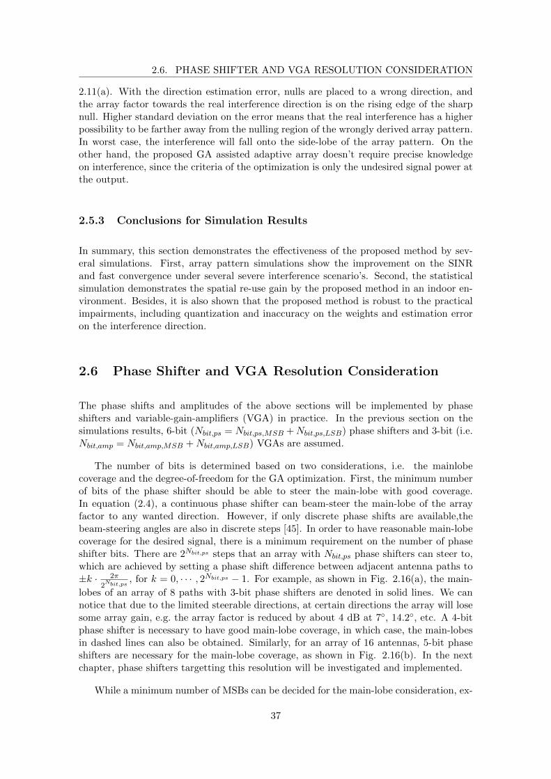
2.6. PHASE SHIFTER AND VGA RESOLUTION CONSIDERATION
2.11(a). With the direction estimation error, nulls are placed to a wrong direction, andthe array factor towards the real interference direction is on the rising edge of the sharpnull. Higher standard deviation on the error means that the real interference has a higherpossibility to be farther away from the nulling region of the wrongly derived array pattern.In worst case, the interference will fall onto the side-lobe of the array pattern. On theother hand, the proposed GA assisted adaptive array doesn’t require precise knowledgeon interference, since the criteria of the optimization is only the undesired signal power atthe output.
2.5.3 Conclusions for Simulation Results
In summary, this section demonstrates the effectiveness of the proposed method by sev-eral simulations. First, array pattern simulations show the improvement on the SINRand fast convergence under several severe interference scenario’s. Second, the statisticalsimulation demonstrates the spatial re-use gain by the proposed method in an indoor en-vironment. Besides, it is also shown that the proposed method is robust to the practicalimpairments, including quantization and inaccuracy on the weights and estimation erroron the interference direction.
2.6 Phase Shifter and VGA Resolution Consideration
The phase shifts and amplitudes of the above sections will be implemented by phaseshifters and variable-gain-amplifiers (VGA) in practice. In the previous section on thesimulations results, 6-bit (Nbit,ps = Nbit,ps,MSB +Nbit,ps,LSB) phase shifters and 3-bit (i.e.Nbit,amp = Nbit,amp,MSB +Nbit,amp,LSB) VGAs are assumed.
The number of bits is determined based on two considerations, i.e. the mainlobecoverage and the degree-of-freedom for the GA optimization. First, the minimum numberof bits of the phase shifter should be able to steer the main-lobe with good coverage.In equation (2.4), a continuous phase shifter can beam-steer the main-lobe of the arrayfactor to any wanted direction. However, if only discrete phase shifts are available,thebeam-steering angles are also in discrete steps [45]. In order to have reasonable main-lobecoverage for the desired signal, there is a minimum requirement on the number of phaseshifter bits. There are 2Nbit,ps steps that an array with Nbit,ps phase shifters can steer to,which are achieved by setting a phase shift difference between adjacent antenna paths to±k · 2π
2Nbit,ps
, for k = 0, · · · , 2Nbit,ps − 1. For example, as shown in Fig. 2.16(a), the main-
lobes of an array of 8 paths with 3-bit phase shifters are denoted in solid lines. We cannotice that due to the limited steerable directions, at certain directions the array will losesome array gain, e.g. the array factor is reduced by about 4 dB at 7, 14.2, etc. A 4-bitphase shifter is necessary to have good main-lobe coverage, in which case, the main-lobesin dashed lines can also be obtained. Similarly, for an array of 16 antennas, 5-bit phaseshifters are necessary for the main-lobe coverage, as shown in Fig. 2.16(b). In the nextchapter, phase shifters targetting this resolution will be investigated and implemented.
While a minimum number of MSBs can be decided for the main-lobe consideration, ex-
37
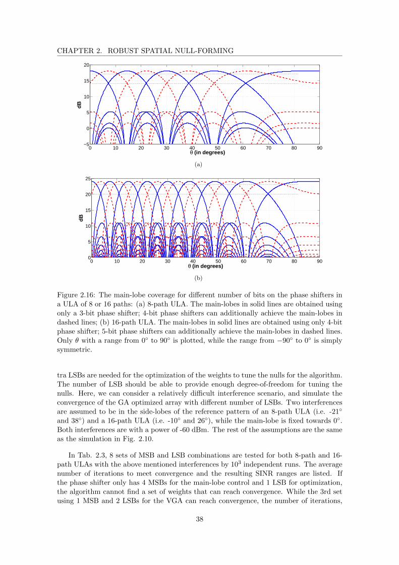
CHAPTER 2. ROBUST SPATIAL NULL-FORMING
0 10 20 30 40 50 60 70 80 90−5
0
5
10
15
20
θ (in degrees)
dB
(a)
0 10 20 30 40 50 60 70 80 900
5
10
15
20
25
θ (in degrees)
dB
(b)
Figure 2.16: The main-lobe coverage for different number of bits on the phase shifters ina ULA of 8 or 16 paths: (a) 8-path ULA. The main-lobes in solid lines are obtained usingonly a 3-bit phase shifter; 4-bit phase shifters can additionally achieve the main-lobes indashed lines; (b) 16-path ULA. The main-lobes in solid lines are obtained using only 4-bitphase shifter; 5-bit phase shifters can additionally achieve the main-lobes in dashed lines.Only θ with a range from 0 to 90 is plotted, while the range from −90 to 0 is simplysymmetric.
tra LSBs are needed for the optimization of the weights to tune the nulls for the algorithm.The number of LSB should be able to provide enough degree-of-freedom for tuning thenulls. Here, we can consider a relatively difficult interference scenario, and simulate theconvergence of the GA optimized array with different number of LSBs. Two interferencesare assumed to be in the side-lobes of the reference pattern of an 8-path ULA (i.e. -21
and 38) and a 16-path ULA (i.e. -10 and 26), while the main-lobe is fixed towards 0.Both interferences are with a power of -60 dBm. The rest of the assumptions are the sameas the simulation in Fig. 2.10.
In Tab. 2.3, 8 sets of MSB and LSB combinations are tested for both 8-path and 16-path ULAs with the above mentioned interferences by 103 independent runs. The averagenumber of iterations to meet convergence and the resulting SINR ranges are listed. Ifthe phase shifter only has 4 MSBs for the main-lobe control and 1 LSB for optimization,the algorithm cannot find a set of weights that can reach convergence. While the 3rd setusing 1 MSB and 2 LSBs for the VGA can reach convergence, the number of iterations,
38

2.6. PHASE SHIFTER AND VGA RESOLUTION CONSIDERATION
Table 2.3: The convergence of the algorithm and optimized SINR range by different num-ber of LSBs. The interferences are assumed with power of -60 dBm and with AoAs of -10
and 26 for the 8-path ULA and -21 and 38 for the 8-path ULA.
MSB LSB MSB LSBAverage
# of iterationsSINR
Range (dB)Average
# of iterationsSINR
Range (dB)
1 4 1 1 1 >1000 16.7 >1000 17.3 to 18.2
2 4 1 2 1 >1000 7.9 >1000 15.1 to 15.3
3 4 1 1 2 207 16.8 to 17.7 420 20.3 to 20.8
4 4 2 1 1 205 17.4 to 17.7 105 20.3 to 20.8
5 4 2 2 1 >1000 10.1 >1000 19.4 to 19.7
6 4 2 1 2 30 17.4 to 17.8 47 20.3 to 20.8
7 4 3 1 1 140 17.2 to 17.7 48 20.3 to 20.8
8 4 3 1 2 26 17.4 to 17.8 34 20.3 to 20.8
Phase Shifter VGA 16-path ULA8-path ULA
Set #
however, is relatively high. Similar results are obtained for 4th set. The 5th set is similarto the 2nd set, in the sense that the 2 MSB and 1 LSB VGA are not giving enough degree-of-freedom to tune the spatial nulls to reach convergence. From the 6th set, convergencespeed is improved and good SINR results are obtained. Interestingly, further increasingthe number of LSBs in the phase shifters can improve the convergence speed, even thoughthe search space is larger.
Overall, the 6th set of the number of bits from the phase shifter and VGA provides goodconvergence performance, with less hardware complexity than set 7 or 8. The bottleneck ismore on the 6-bit phase shifter rather than the 3-bit VGA, since the discrete phase shiftersat mm-wave frequencies found in literatures are not more than 5-bit [45, 46]. Notice thatthe algorithm doesn’t require accurate 6-bit phase shifts, as it has been demonstrated inFig. 2.15. Instead, it is more important to have interpolated finer phase shift steps forthe algorithm to globally tune the setting to minimize the undesired received power.
Actually, with these considerations, IQ-modulated phase shifters can also be an inter-esting candidate for the weight control [39, 47, 48]. The IQ-modulated phase shifter com-bines two quadrature signals by different amplitudes to achieve certain phase/amplitude.The difference of the weights achieved by the IQ-modulated phase shifter and traditionalphase shifter is shown by the constellation plot in Fig. 2.17. Only the first quadrant isplotted for simplicity. In Fig. 2.17, circular points are the constellation points of a 6-bitphase shifter in combination with a 3-bit VGA, while the dotted points are by the IQmodulation with 3-bit amplitude levels (i.e. 7 non-zero levels) for both I and Q. We cansay that they are evenly distributed in a Polar coordinate and a Cartesian coordinate.Referring back to the proposed method in this chapter, the adjustment on the LSBs bythe algorithm is equivalently searching around a MSB weight. For example, if (1,0) is theMSB setting, the algorithm will search around the dashed box and the solid box for the
39
CHAPTER 2. ROBUST SPATIAL NULL-FORMING
0 10
1
I
Q
Figure 2.17: The constellation points in the first quadrant achieved by a phase shifterwith a VGA (circles) and I/Q modulation (dots) respectively. If (1, 0) is the MSB settingfor the weight on one of the antenna paths, what the GA optimization does is tune thissetting within the boxes for the two types of weight controls.
Table 2.4: The convergence of the algorithm and optimized SINR range by sets of con-stellations points from Fig. 2.17. The simulation setup is the same as in Tab. 2.3.
Average# of iterations
SINRRange (dB)
Average# of iterations
SINRRange (dB)
30 17.4 to 17.8 47 20.3 to 20.8
47 17.3 to 17.8 43 20.3 to 20.8
6-bit Phase shifter + 3-bit VGA
3-bit I/Q Modulation
8-path ULA 16-path ULA
Polar and Cartesian implementations respectively. They have a comparable tuning range,while the Cartesian implementation has slightly less points. If we test them similarly asthe simulation for Tab. 2.3, we can find that they have comparable performance in termsof convergence and SINR for these two sets of constellation points (Tab. 2.4).
2.7 Summary and Conclusions
In this chapter, an adaptive array with genetic algorithm (GA) is presented for spatialco-channel interference mitigation to facilitate the co-existence for future 60 GHz appli-cations. In practice, the null-forming of an analog/RF phased array can be degradedby practical impairments in the phase shift or amplitude control, or in the directions ofinterferences. To achieve robust null-forming, an adaptive array assisted by a fast GA
40

2.7. SUMMARY AND CONCLUSIONS
optimization is proposed, which can efficiently find the proper weights to decrease thereceived undesired power, so increasing the SINR. It is demonstrated through simulationsthat this method can improve the SINR in different interference situations including inter-ferences relatively close in angle-of-arrival to the desired signal. Furthermore, the array iscapable of adjusting the number of working antenna paths and finding the near-optimumselection and weigthings. The spatial selectivity is further improved compared to the fixedULA of the same size. It is also shown that the method is robust to weight errors. Weexpect it can be a useful method for future standards to exploit the spatial selectivity asan extra resource, which can help co-existence and increase the total network throughputefficiently.
The proposed method in this chapter requires a high resolution phase shifter. This isnecessary to have a good main-lobe coverage for a ULA of 8 or 16 elements, meanwhileproviding extra degrees-of-freedom so that the null-forming array is able to tune the arraypattern to place nulls to certain directions. It is shown that it is desired to have 6-bit phaseshift resolution or comparable I/Q modulated tunable constellation points. In the nextchapter, phase shifters in CMOS technology will be investigated and designed to satisfythe requirement for the analog/RF null-forming arrays.
41

CHAPTER 2. ROBUST SPATIAL NULL-FORMING
42

Chapter 3
High Resolution Phase Shifters forNull-Forming Phased Arrays
3.1 Introduction
In the previous chapter, a robust method to adaptively generate spatial nulls in a 60 GHzphased array is described. In order to form nulls for different situations and with fastconvergence, a high resolution phase shifter is required for the tuning. At the end of thelast chapter, it is claimed that a 3-bit variable gain amplifier VGA in combination with a6-bit phase shifter is desired, i.e. a phase tuning step of about 5.6. An I/Q modulatedphse shift with 3-bit on both I and Q levels is also capable of providing the requiredperformance. In this chapter, two high resolution phase shifters are designed that can beused in the adaptive null-forming array introduced in Chapter 2.
Recent state-of-the-art silicon-based phase shifter designs at millimeter-wave (mm-wave) frequency ranges are reviewed in section 3.2. In section 3.3, the sliding-IF archi-tecture used in this chapter is described and possible phase shifting implementations arediscussed. In sections 3.4 and 3.5, two high resolution phase shifter designs are presentedwith measurement results. The performance of these two phase shifters is summarized insection 3.6, with a discussion on a comparison and benchmarking to the reported phaseshifters in literature. Finally, conclusions are presented in section 3.7.
3.2 State-of-the-Art
In recent publications, many phased array systems are demonstrated at mm-wave frequen-cies [39, 33, 36, 49]. Most of the phased array systems mainly make use of the phasedarray to coherently combine the desired signal towards or from a certain direction. Thisis necessary to compensate for the high path loss and satisfy the link budget at mm-wavefrequencies. For a phased array of small or medium size (e.g. 4 or 8 elements, in [49]and [36]), the main lobe of the antenna pattern is relatively wide, in which case a 4-bitresolution is typically sufficient for main lobe coverage. This has been also demonstrated
43

CHAPTER 3. HIGH RESOLUTION PHASE SHIFTERS
Figure 3.1: The different phase shifter implementations, including RFPS, LOPS, BBPSand digital PS. For simplicity, a receiver phased array front end with single stage mixingis shown.
in Fig. 2.16(a).
The implementation of phase shifters can be at various locations in a front end. Typicallocations for phase shifters are in the RF path (RFPS), in the LO path (LOPS), in thebaseband (BBPS) or during digital processing (Digital PS), as demonstrated in Figure3.1.
While a digital PS has the most flexibility and is commonly used at lower frequenciesand/or for professional applications, it requires N (which is the number of antennas)analog-to-digital converters (ADCs). For the applications in the mm-wave frequency range,the targeted bandwidth is in the GHz range (e.g. 2-9 GHz of bandwidth in the IEEE802.11.ad 60GHz WLAN standard [12]), which requires a power hungry ADC. Multiplepower hungry ADC’s will lead to an exceedingly large power consumption for the digitalPS architecture.
The RFPS shown in Figure 3.1 is adopted in [33, 48]. It can reduce the number ofmixers compared to the other architectures, with a potential reduction of the power con-sumption and hardware complexity. However, the RFPS and combiners at RF frequencycan directly degrade the signal, in terms of gain, noise figure (NF) or linearity. The passivereflection-type RFPS in [39] introduces a loss of 4 dB to 7.5 dB after the LNA, which candegrade the total gain and NF. Extra active combiners are used to compensate the loss
44

3.3. A 60 GHZ SLIDING-IF FRONT-END ARCHITECTURE
from the RFPS and combiner networks. The 4-bit active RFPS in [36] consumes about27 mW of power.
The LOPS architecture is an alternative, such as in [39, 46]. On the one hand, thephase shifter implementation of a LOPS is decoupled from the signal path and will notdirectly influence the signal path quality, such as gain, NF and linearity. This relaxes thedesign of the LOPS. On the other hand, however, the high frequency distribution networkfor the LO signal to each mixer will increase the complexity, which also holds for the BBPSas shown in Fig. 3.1.
The BBPS is also an interesting option, which works at much a lower frequency thanRFPS and LOPS. As a result, in principle, the BBPS has the potential of high resolutionand low power. The receiver baseband section with beamforming functionality in [37]demonstrates a phase shift resolution of 6.8.
A summary on the phase shifters in literatures can be found in Table. 3.1.
In this chapter, the main target of the phase shifter design is to achieve a high resolution(6-bit) according to the work in chapter 2. From the discussion on different phase shifterimplementations in Fig. 3.1, the LOPS and BBPS are two interesting candidates. TheLOPS is decoupled from the signal path and can have less impact on the signal qualitywhile achieving a high resolution. Besides, as will be shown in the next sections, a sliding-IF front-end architecture will be used, in which case an LOPS architecture making use ofthe frequency division can be designed without adding much extra hardware to the frontend. For the BBPS it is in general easier to achieve a high resolution due to the much loweroperating frequency. In addition, the power consumption is expected to be relatively low.So in this chapter, we will focus on these two options, and two solutions are implementedseparately for comparison, i.e. LOPS and BBPS.
Before presenting the phase shifter designs, the sliding-IF receiver front end in whichthey will be used is described in the following section.
3.3 A 60 GHz Sliding-IF Front-End Architecture
Fig. 3.2 shows the single-path 60 GHz sliding-IF receiver front end. The signal pathconsists of an LNA and two mixing stages. The RF and IF mixers are driven by a 48 GHzLO (fLO) and its divided-by-4 version at 12 GHz respectively, as shown in the LO path.This architecture requires a reduced LO frequency, i.e. 48 GHz instead of 60 GHz for adirect conversion architecture. At the same time, from the frequency divider-by-4, near-perfect quadrature signals can be obtained, because both I and Q outputs are triggeredby the rising edge of the divider input. A similar sliding-IF architecture with 40 GHz LOsignal and frequency divider-by-2 can further reduce the required LO frequency, but theI/Q balance can be degraded, e.g. due to a non-50% duty cycle LO signal. As a result,the architecture shown in Fig. 3.2 is chosen.
In order to extend the sliding-IF receiver architecture into a phased array configuration,phase shifters and combiners need to be implemented at certain location, as discussed inthe last section in Fig. 3.1. In the sliding-IF architecture, since there are two mixing
45

CHAPTER 3. HIGH RESOLUTION PHASE SHIFTERS
Figure 3.2: The 60 GHz sliding-IF receiver front-end architecture.
stages, an alternative of doing phase shift is at the intermediate frequency (IF), i.e. at 12GHz in this case. It can operate at a lower frequency than the RFPS. However, the LOPSand BBPS are chosen here in order to take advantage of (1) the frequency divider-by-4operation and (2) the I/Q signals at the baseband. The details and advantages of thetwo chosen topologies will be explained in the following sections. In the next section, twoseparate phase shifter designs will be presented, i.e. a LOPS and a BBPS.
3.4 LO-Path Phase Shifter
3.4.1 Architecture
For a LOPS, variable phase shifts in the LO signal will be applied to the signal after themixing operation. Assume an input signal at the input of a mixer as As cos(2πfst + φs),and an LO at the other input of the mixer as cos(2πfLOt + φLO + ∆φLOPS), where fsand fLO are the signal and LO frequencies, φs and φLO are their phases, and ∆φLOPS isthe tunable phase shift in the LO signal. After the mixing operation, the output can bederived as:
GmixerAs cos(2πfst+ φs) cos(2πfLOt+ φLO + ∆φLOPS)
where Gmixer is the gain of the mixer. Ignoring the the other frequency components byproper filtering, the down-converted output can be simplified as:
GmixerAs cos [2π(fs − fLO)t+ φs − φLO −∆φLOPS ]
This implies that the phase shifts in the LO-path can be transferred to the outputsignal. As previously discussed, the LOPS has the advantage of being decoupled from thesignal path, and it has less requirements on the noise and linearity. However, it is stillworking at a relatively high frequency. In the following paragraphs, a LOPS in a sliding-IFreceiver front end is proposed, targeting for high resolution.
In the sliding-IF architecture shown in Fig. 3.2, the LO path uses a frequency divider-by-4 to generate the 12 GHz signal for the IF mixer. It is interesting to notice thatfrom a frequency divider-by-4 (FD4), a 3-bit phase shift is already available. A typicalconventional static frequency divider-by-2 (FD2) consists of two latches (as shown in the
46

3.4. LO-PATH PHASE SHIFTER
48GHz LOPSA
Inv.PSA
48GHz
12GHz IQ
60GHz sliding-IF receiver front end
LOPS(Section 4.4)
I
Q
LNA RF Mixer
IF Mixer
Tline
÷2(FD2)
÷2(FD2)
Figure 3.3: The 60 GHz LO-path phase shifter architecture in the sliding-IF receiver frontend.
next section 3.4.2), and the phases of the outputs of the two latches are 90 out-of-phaseat the divided frequency, i.e. at 24 GHz. Passing either signal to the next FD2, a 45
phase difference can be distinguished at 12 GHz. In a differential topology, a 180 phaseshift can be achieved simply by inverting the differential connections.
The already available 3-bit phase shift from the FD4 can be used for a LOPS design,to reduce the extra hardware and power consumption. Extra multiplexers are required toselect either output from the static FD2’s, but they also act as buffers between dividersand before the IF mixer, which are necessary anyway.
In order to achieve a 6-bit phase resolution, the three least significant bits are stillmissing. Notice that in order to evenly distribute the centrally generated 48 GHz LOsignal to each front-end path, a tree-like distribution network is typically used. Actuallywe can use part of the distribution transmission line, and by making it tunable, such asin [50, 51], fine phase tuning steps can be achieved.
From the discussion above, the proposed LO phase shifter is shown in the dashedbox in Fig. 3.3, consisting of a 48 GHz tunable transmission line (Tline), two frequencydividers-by-two (FD2) and two phase selection amplifiers (PSA). The first PSA selectseither the I or Q output at 1
2fLO from the first FD2, which corresponds to 0 or 45 at14fLO after the second FD2. Besides selection, the second PSA is also capable of invertingthe phase. The two FD2’s in combination with the two PSA’s achieve a 45 phase shiftresolution (3-bit).
The finer phase shift steps are adjusted by the tunable Tline. Thanks to the FD2’sand PSA’s, a reduced phase tuning range is required for the Tline, so it requires a smallerarea. Assume that the Tline’s tuning range is 4φ, then the 12 GHz output of the secondPSA can be phase shifted by 4φ4 +N ·45, where N = 0, · · · , 7. The total phase shift fromthe RF and IF mixers incurs to the baseband output is 5
4 · 4φ+N · 45, which needs tocover 360, so we can derive that the required tuning range for the tunable Tline is only4φ = 36. The tunable Tline does not significantly add to the total silicon area because itcan be part of the LO distribution network, which is necessary to distribute the centrallygenerated LO signal to the mixers in each path of a phased array front end. Furthermore,
47

CHAPTER 3. HIGH RESOLUTION PHASE SHIFTERS
...
...
Total length of tot and Nsec sections
Section length of sec
(a)
...
...
Lsec
Csec
Csw
Lsec
Csec
Csw
Lsec
Csec
Csw
Total length of tot and Nsec sections
Section length of sec
(b)
Figure 3.4: (a). Schematic of the tunable transmission line. (b). Model of the tunabletransmission line.
in a phase array context, the local frequency divider before each IF mixer can help to avoiddistributing the 12 GHz I/Q signals. Only a 48 GHz distributing network is necessary forthis phase shifting architecture.
3.4.2 Circuit Description
In this section, the design details of the circuits in Fig. 3.3 are described.
(a) Tunable Transmission Line
The principle of the tunable transmission line for fine phase steps can be explained by Fig.3.4(a). In the schematic, a single-ended Tline is periodically loaded by a shunt capacitor inseries with a switch. By controlling the number of switches that are tuned on, the effectivepropagation speed of the Tline is changed. As a result, with a fixed physical length, thephase shift across the Tline can be tuned.
Trade-offs exist in the design of this tunable Tline, between length, phase tuning rangeand impedance mismatch. This can be better illustrated by analysing a simplified lumpedmodel shown in Fig. 3.4(b). The total physical length of the Tline is assumed to be ltot,and Nsec sections are equally divided and loaded with a switched capacitor (CSW ). In our
48

3.4. LO-PATH PHASE SHIFTER
case, as aforementioned, a phase tuning range (4φ) of at least 36 with 3-bit is requiredfrom this tunable Tline, which means Nsec > 8. A small section of ideal Tline can besimplified by a lumped LC model with good accuracy, as shown in Fig. 3.4(b). The phasetuning range of this Tline is the phase shift difference between the all-on state and theall-off state. When all switches are off, the phase shift at the interest frequency f0 is:
φOFF = βOFF · ltot (3.1)
where : βOFF = 2πf0 ·√Lseclsec· Cseclsec
= 2πf0 ·√Lsec · Csec ·
Nsec
ltot
For the all-on state, the total shunt capacitance at each section becomes Csec+CSW =Csec ·Ratio, where we assume an on-off capacitance ratio of Ratio. Similarly as (3.1), thetotal phase shift when all switches are on is:
φON = βON · ltot (3.2)
where : βON = 2πf0 ·√Lsec · Csec ·
Nsec
ltot·√Ratio
Subtracting (3.1) from (3.2) will give the phase tuning range:
4φ = φON − φOFF= 2πf0 ·
√Lsec · Csec ·Nsec · (
√Ratio− 1)
(3.3)
Increasing Ratio can lead to a larger tuning range. However, it will also increase theimpedance variation between the all-on and all-off states. The characteristic impedancesof the Tline during all-on and all-off states are:
Z0,OFF =
√LsecCsec
(3.4)
Z0,ON =
√Lsec
Csec ·Ratio(3.5)
A larger Ratio will reduce Z0,OFF , and can cause impedance mismatch. The Tlinecan be designed in such a way that it satisfies Z0 = 1
2(Z0,ON +Z0,OFF ), where Z0 = 50 Ωis the single-ended system impedance. This gives less input reflection variation over thetuning range. From (3.4) and (3.5), it follows:
Z0 =1
2
√LsecCsec
· (1 +1√Ratio
) (3.6)
Another boundary is set by the unloaded Tline when all switches are turned off. For anunloaded Tline, the propagation speed and wavelength are typically constant and deter-mined mainly by the effective dielectric constrant εeff,OFF . For a conventional co-planarwaveguide on-chip Tline, the value of εeff,OFF is typically between dielectric constant of
49

CHAPTER 3. HIGH RESOLUTION PHASE SHIFTERS
the on-chip dielectric (≈ 4.2) and the dielectric constant of the silicon substrate (≈ 11.9).It can have a much larger value (> 11.9) if slow-wave technique is adopted in the Tline[52]. The wavelength of the unloaded Tline is λOFF = 2π
βOFF. The εeff,OFF can be derived
as:√εeff,OFF =
λ0
λOFF=c0 ·√LsecCseclsec
(3.7)
where c0 is the speed of light, and λ0 is the wavelength at f0 in air. From (3.3) and (3.7),we have:
4φ = 2π · ltotλ0· √εeff,OFF · (
√Ratio− 1) (3.8)
From (3.8), we can observe the relation-ship between the phase tuning range (4φ),physical length (ltot) and the on-off capacitance ratio (Ratio). In general, the tuning rangecan be increased by a longer Tline and/or higher Ratio. If area is not a problem, to havethe same 4φ, larger ltot with lower Ratio can have a more stable Tline impedance fordifferent tuning status, as derived in (3.4), (3.5) and (3.6). On the other hand, the areacan be reduced by using a higher Ratio, or larger CSW . However, Ratio shouldn’t be toolarge, otherwise impedance variation can be too large and cause amplitude variation.
Another interesting observation from (3.8) is that a higher εeff,OFF can also reducethe length while achieving the same phase tuning range and using the same Ratio. Soa slow-wave structure in the unloaded Tline is preferred, which will be described in thefollowing paragraphs.
The more detailed schematic of the tunable Tline is demonstrated in Fig. 3.5. TheTline is implemented with a differential structure, as shown in the dashed box. In thisdesign, twelve sections with a total tuning range of 46 are designed, i.e. Nsec = 10and 4φ = 46, in order to intentionally leave some design margin in case of inaccuraciesfrom EM simulations and/or process spread. In order to reduce the line length whilemaintaining the same tuning range, a slow-wave structure and a large Ratio ratio areused. However, this leads to a larger impedance change upon switching. The matchingnetwork between the TLine and the divider cannot be optimal for all line impedances inthe various switching states. To achieve low reflection variation, an LC matching networkis designed to have Zi div matched to an intermediate value of Zo line, calculated as theaverage between the impedance values when Non,sw = 0 and Non,sw = 12.
At the input to the FD2, differential lines with weak capacitive coupling to the LOlines are inserted for measuring the relative phase shift tuning achieved by the Tline. Byoverlapping the LO and testing lines in two adjacent metal layers, a coupling factor ofabout -25 dB is achieved without much influence on the LO signal. This capacitivelycoupled differential line is terminated by 100 Ω on one side, and goes to a differentialoutput pad through a 100 Ω Tline on the other side, as shown in Fig. 3.5.
The layout of the designed tunable Tline is shown in Fig. 3.6. As shown in Fig.3.6(a), the co-planar waveguide (CPW) tunable Tline has a ground-signal-signal-ground(GSSG) configuration with a total length of 250 µm. It has grounded stripes in metal1 which provides the slow-wave effect and increases the effective dielectric constant. Ineach section, the Tline is loaded with two interdigital capacitors and a switch, which are
50

3.4. LO-PATH PHASE SHIFTER
...
...
Mat
chin
g
To input pads
+
-
To divider
To output pads for relative phase
measurement
+
-
100 Ω
Tunable Tline
+ -
Figure 3.5: The tunable transmission line loaded with switched capacitors, the interstagematching and the weak capacitive coupled output line for relative phase measurement.
shown in Fig. 3.6 (c) and (d) respectively. The multi-layer interdigital capacitor in theused technology (40 nm CMOS) can provide high capacitance density, thanks to the finefinger width and spacing (0.063 µm). The maximum capacitance density is 2.8 fF/µm2 ifmetal 1 to metal 5 are used. In our design, metal 2 to metal 5 are used (with a capacitancedensity of 2.2 fF/µm2) to reduce the parasitic capacitance to the substrate.
(b) Frequency Dividers
The static FD2’s are implemented by cascading two current-mode-logic latches (L1 andL2) with an inverted feedback from the output of L2 to the input of L1, as shown inFig. 3.7(a). Fig. 3.7(b) shows the schematic of the latch with inductive peaking at theload for higher working frequency. The second FD2, however, works at lower frequency,and the peaking inductor can be excluded in order to save area and avoid unnecessarymagnetic coupling which may cause I/Q imbalance. For the same reasons, the inductoris desired to have a small area. The peaking inductor in the first FD2 is designed asa two-layer-stacked inductor with two turns in each layer. Effectively, it is a four-turninductor. The two stacked layers are not overlapping directly, in order to reduce theparasitic capacitance. Meanwhile, due to the skin-effect, the current crowded along theedges is still strongly coupled between turns, so the self inductance is not reduced toomuch. As a result, the custom four-turn inductor can achieve a higher inductance valueat the output frequency with a more compact layout. The layout of the custom inductoris shown in Fig. 3.8, with a width of about 69 µm. In addition, the tail current source isexcluded in the latches in Fig. 3.7(b) due to the limited voltage headroom.
(c) Phase Selection Amplifiers
As shown in Fig. 3.9, the PSAs are implemented by two cascode amplifiers in parallelwith the I and Q signals from the divider as the inputs, and the cascode transistors asswitches to pass either current to the output load. The cross-connected pairs M2/M3 andM6/M7 are for phase inverting in the second PSA controlled by s2 and s4 respectively.
51

CHAPTER 3. HIGH RESOLUTION PHASE SHIFTERS
Csw1
Csw2
SW
Control
Csw2 Csw1
( a )
( b )
( c )
( d )
Metal 5- + - ++
Metal 5Metal 4Metal 3Metal 2
+ - + --
- + - ++
+ - + --
Metal 4
Metal 3
Metal 2
Figure 3.6: Design details of the tunable transmission line. (a) The tunable TLine isin ground-signal-signal-ground (GSSG) co-planar-waveguide (CPW) configuration, withslow-wave technique, and it consists of 12 sections. (b) In each section, the Tline is loadedwith shunt capacitors (CSW1 and CSW2) and a switch (SW). (c) The 3-D view and cross-section view of the multi-layer interdigital capacitor used as CSW1 and CSW2. (d) Theschematic of the switch.
52

3.4. LO-PATH PHASE SHIFTER
+
I
-
D+ Q+
D- Q-
CLK+ CLK-
D+ Q+
D- Q-
CLK+ CLK-
in
+
Q
-
L1 L2
(a)
Q-
D+ D-
CLK+ CLK-
Q+
M1 M2M3 M4
Vdd Vdd
(b)
Figure 3.7: (a). Block diagram of the static frequency dividers-by-2 (FD2’s), consistingof two current-mode-logic latches (L1 and L2); (b). Schematic of the latch with inductivepeaking.
These phase-inverting transistors are not required in the first PSA. Besides the selectionfunction, the PSA’s have simulated voltage gains of 6.9 dB and 8.0 dB around 24 GHzand 12 GHz respectively. So they also act as buffer stages between the dividers and theIF mixer.
3.4.3 Measurement Results
The proposed phase shifter is designed and fabricated in 40-nm low-power CMOS technol-ogy from GLOBALFOUNDRIES. This process has a standard baseline back-end, with 6copper metal layers and 1 aluminum top metal. EM simulations in ADS Momentum [53]and modeling are done on the passive components to capture the high frequency perfor-mance. The chip photo is shown in Fig. 3.10, with an active area of 550 µm× 260 µm.The length of the tunable Tline is about 250 µm. Excluding the output buffer, the chipconsumes 16.9 mW from a power supply of 1.2 V. Each of the FD2 consumes only 3.8mW, which is considerably lower than other static dividers in the similar frequency range[54] [55].
53

CHAPTER 3. HIGH RESOLUTION PHASE SHIFTERS
69 µm
Top metal
2nd
Top metal
Metal 1Shielding
Figure 3.8: The peaking inductor used in the first FD2 (Fig. 3.7(b)). It is a stackedinductor in the two top metal layers, and with two turns in each layer. Grounded metalstripes in metal 1 are used underneath for shielding from the lossy substrate.
in1+ in1- in2+ in2-
s1 s1s2 s3 s3s4M1 M2 M3 M4 M5 M6 M7 M8
Vdd
Figure 3.9: The second phase selection amplifier (PSA), with phase inverting capability.For the first PSA, transistors M2, M3, M6 and M7 are excluded.
(a) Standalone Passive Structures
In order to verify the performance of the critical passive structures characterized byEM simulations, some standalone structures are independently taped-out and measured.Shown in Fig. 3.11 are the differential inductor from Fig. 3.8 and the tunable Tline fromFig. 3.6. The RF differential pad and tapering are first characterized by open-short-loadconfigurations (not shown in the figure) and de-embedded from the measured results ofFig. 3.11. So the reference plane is moved to the input and output of the test structures,as shown in the figure.
54

3.4. LO-PATH PHASE SHIFTER
Figure 3.10: Chip micrograph.
Reference plane
Reference plane
Figure 3.11: Passive structures for testing. Left: differential inductor in Figure 3.8. Right:tunabe Tline in Fig. 3.6.
As shown in Fig. 3.12, the measurement results of the inductance and quality factorfit to the simulation results quite well. Especially the self-inductance (low frequencyinductance) and the resonance frequency are very accurate. There is some minor deviationbetween the measured and simulated quality factor (10 versus 8).
55

CHAPTER 3. HIGH RESOLUTION PHASE SHIFTERS
Qua
lity
Fac
tor
Inductance (H)
Frequency (GHz)
Figure 3.12: The measured and simulated inductance and quality factor of the custominductor shown in Fig. 3.8. Smooth curves are simulated results, and curves with ripplesare measured results.
Frequency (GHz) Frequency (GHz)
All-OFF All-ON
Z0 (Ohm)
Loss (dB/mm)
Z0 (Ohm)
Loss (dB/mm)
∠∠∠∠S21 ( ° ) ∠∠∠∠S21 ( ° )
Figure 3.13: Measurement and simulation results of the tunable Tline, including the char-acteristic impedance (Z0), line loss per millimeter and phase shift across the line (φ(S21)).Plots on the left column are results when all switches are off, while on right column arefor the all-on state.
56
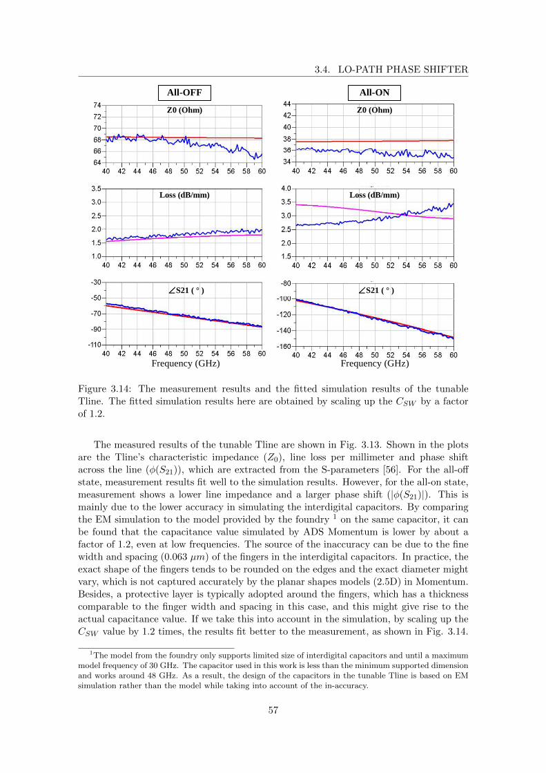
3.4. LO-PATH PHASE SHIFTER
Frequency (GHz)
All-OFF All-ON
Z0 (Ohm)
Loss (dB/mm)
Z0 (Ohm)
Loss (dB/mm)
∠∠∠∠S21 ( ° ) ∠∠∠∠S21 ( ° )
Frequency (GHz)
Figure 3.14: The measurement results and the fitted simulation results of the tunableTline. The fitted simulation results here are obtained by scaling up the CSW by a factorof 1.2.
The measured results of the tunable Tline are shown in Fig. 3.13. Shown in the plotsare the Tline’s characteristic impedance (Z0), line loss per millimeter and phase shiftacross the line (φ(S21)), which are extracted from the S-parameters [56]. For the all-offstate, measurement results fit well to the simulation results. However, for the all-on state,measurement shows a lower line impedance and a larger phase shift (|φ(S21)|). This ismainly due to the lower accuracy in simulating the interdigital capacitors. By comparingthe EM simulation to the model provided by the foundry 1 on the same capacitor, it canbe found that the capacitance value simulated by ADS Momentum is lower by about afactor of 1.2, even at low frequencies. The source of the inaccuracy can be due to the finewidth and spacing (0.063 µm) of the fingers in the interdigital capacitors. In practice, theexact shape of the fingers tends to be rounded on the edges and the exact diameter mightvary, which is not captured accurately by the planar shapes models (2.5D) in Momentum.Besides, a protective layer is typically adopted around the fingers, which has a thicknesscomparable to the finger width and spacing in this case, and this might give rise to theactual capacitance value. If we take this into account in the simulation, by scaling up theCSW value by 1.2 times, the results fit better to the measurement, as shown in Fig. 3.14.
1The model from the foundry only supports limited size of interdigital capacitors and until a maximummodel frequency of 30 GHz. The capacitor used in this work is less than the minimum supported dimensionand works around 48 GHz. As a result, the design of the capacitors in the tunable Tline is based on EMsimulation rather than the model while taking into account of the in-accuracy.
57
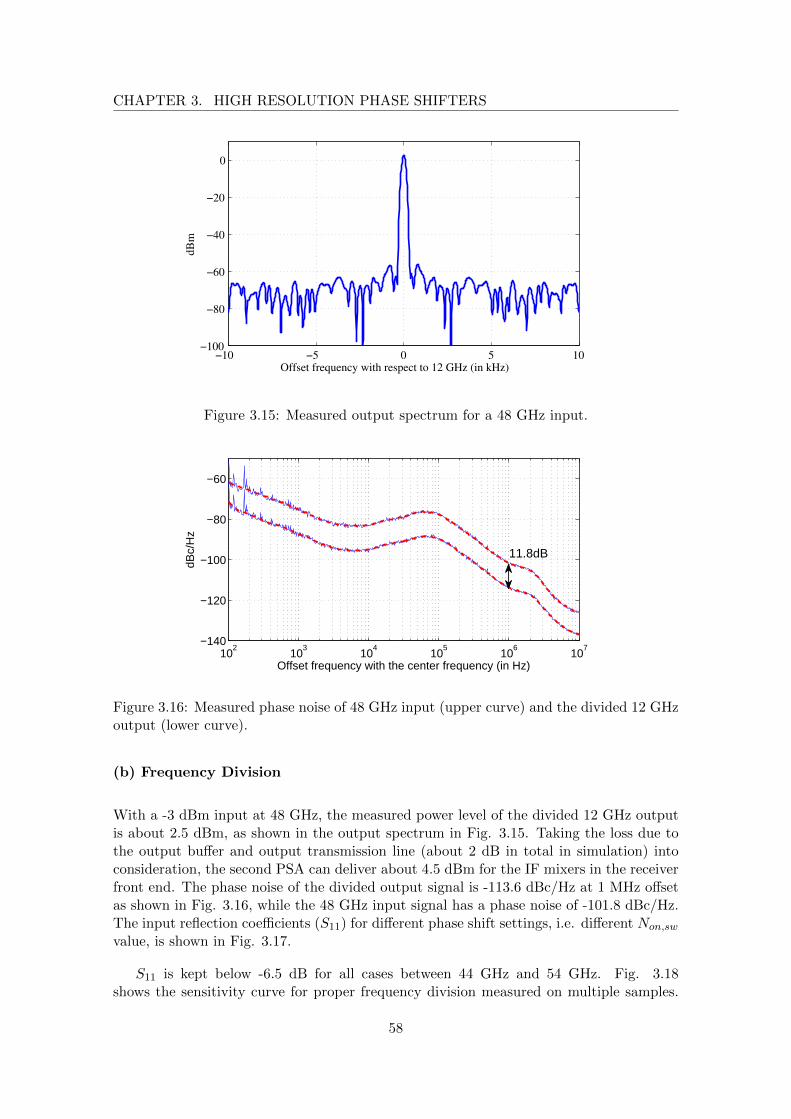
CHAPTER 3. HIGH RESOLUTION PHASE SHIFTERS
−10 −5 0 5 10−100
−80
−60
−40
−20
0
Offset frequency with respect to 12 GHz (in kHz)
dB
m
Figure 3.15: Measured output spectrum for a 48 GHz input.
102
103
104
105
106
107
−140
−120
−100
−80
−60
Offset frequency with the center frequency (in Hz)
dBc/
Hz
11.8dB
Figure 3.16: Measured phase noise of 48 GHz input (upper curve) and the divided 12 GHzoutput (lower curve).
(b) Frequency Division
With a -3 dBm input at 48 GHz, the measured power level of the divided 12 GHz outputis about 2.5 dBm, as shown in the output spectrum in Fig. 3.15. Taking the loss due tothe output buffer and output transmission line (about 2 dB in total in simulation) intoconsideration, the second PSA can deliver about 4.5 dBm for the IF mixers in the receiverfront end. The phase noise of the divided output signal is -113.6 dBc/Hz at 1 MHz offsetas shown in Fig. 3.16, while the 48 GHz input signal has a phase noise of -101.8 dBc/Hz.The input reflection coefficients (S11) for different phase shift settings, i.e. different Non,sw
value, is shown in Fig. 3.17.
S11 is kept below -6.5 dB for all cases between 44 GHz and 54 GHz. Fig. 3.18shows the sensitivity curve for proper frequency division measured on multiple samples.
58

3.4. LO-PATH PHASE SHIFTER
42 44 46 48 50 52 54 56−30
−25
−20
−15
−10
−5
0
frequency (GHz)
S11
(dB
)
Figure 3.17: Measured S11 versus the tunable Tline’s control.
42 44 46 48 50 52 54 56−12
−10
−8
−6
−4
−2
0
2
freq (GHz)
Sen
sitiv
ity (
dBm
)
sample 1sample 2sample 3sample 4sample 5
Figure 3.18: Measured input sensitivity for the frequency division.
The divider-by-4 is not designed with self resonance around the center frequency as moststatic frequency dividers do, which is due to the minimized current in the latches for lowpower consumption. However, the minimum required power level of less than -2 dBm forinput frequencies from 44 GHz to 54 GHz is not an issue for normal LO generation withbuffer stages.
(c) Phase Shift
The phase shift steps achieved by the tunable Tline for different Non,sw are shown in Fig.3.19. The plotted phase shifts are referred to the phase response when Non,sw = 0. Thephase shift by the tunable Tline results in a tuning range of 44.3 to 59.5 for frequenciesbetween 44 GHz and 54 GHz, with a maximum and average phase shift step of 5.4 and3.5 respectively. This corresponds to about 6-bit phase shift resolution. The total phaseconstellation points are plotted in Fig. 3.20, including the 45 phase steps tuned by the
59

CHAPTER 3. HIGH RESOLUTION PHASE SHIFTERS
42 44 46 48 50 52 54 56−60
−50
−40
−30
−20
−10
0
frequency (GHz)
phas
e sh
ift (
°)
Figure 3.19: Measured tunable Tline’s phase shifts, relative to the phase response whenall switches are tuned on.
30
210
60
240
90
270
120
300
150
330
180 0
Figure 3.20: The phase shift constellation points at 48 GHz, including tunable Tline’sphase shift and N × 45 phase shift steps by the PSA’s.
PSA’s which are denoted as solid dots. The denser points around the solid dots are dueto the more than 36 phase shift range of the tunable Tline.
60

3.5. BASEBAND PHASE SHIFTER
RF Mixer
÷448GHz LO
12GHz, I
12GHz, Q
a1
a2
-a2
a1
IF Mixer
IQ-mod Phase Shifter
Divider-by-4
LNA
Baseband IQmod PS(Section 4.5)
BB, I
BB, Q
(a)
(b)
Figure 3.21: (a). The 60 GHz sliding-IF receiver front-end architecture and the basebandI/Q modulated phase shifter. (b). I/Q modulated phase shifting.
3.5 Baseband Phase Shifter
3.5.1 Architecture
In Fig. 3.2, from the I/Q IF mixers, there are quadrature signals available, which can beused to generate different phase shifts by I/Q modulation. In this way, we can have a BBPSworking at much lower frequency, to achieve high resolution and low power consumption.The proposed baseband phase shifter is shown in Fig. 3.21(a). The proposed basebandphase shifter utilizes the quadrature signals from the I/Q mixers in order to generate themodulated phase shifts and amplitudes by combining the IF I and Q signals with certainratios, as shown in Fig. 3.21(b).
3.5.2 Circuit Description
Figure 3.22 shows the top level schematic of the baseband phase shifter. Only one com-bining pair (for either I or Q output) is shown for simplicity. It includes differential Iand Q IF mixers each loaded with a resistor chain at the output, which allows uniformly
61

CHAPTER 3. HIGH RESOLUTION PHASE SHIFTERS
Figure 3.22: The baseband I/Q modulated phase shifter testchip with 12 GHz I/Q mixersand polyphase filter.
interpolating of the output voltage. A level selection gm-cell is inserted at each series re-sistor in the chain with enabling controls so that one of the voltage levels can be selectedand converted into current. By enabling one of the gm-cells in the I and Q resistor chainsrespectively, certain levels of I and Q outputs are selected and further combined in the cur-rent domain. As a result, the modulated signals with different phase shifts and amplitudescan be generated. The topology can be scaled to higher resolutions by simply increasingthe number of interpolating resistors, meanwhile maintaining the power consumption andaccuracy.
Each node along the resistive chain shares the same DC voltage, so that no DC currentflows through the resistors. The common voltage along the resistor chain provides at thesame time biasing for the gm-cells. Notice that the dummy gm-cell for zero amplitudeselection is necessary for maintaining proper DC biasing at the output.
Eight levels are implemented on the test chip with 7 resistors in each resistor chain.Notice, however, that the proposed topology can be easily extended to higher numberof levels without extra power consumption. Also implemented on the test chip is a twostage RC polyphase filter, generating quadrature LO signals for the I/Q mixers for testingpurposes. In the actual system, the I/Q outputs of the divider will be used instead.
The I/Q mixers use a Gilbert cell double-balanced topology, as shown in Fig. 3.23. Atthe source of the input transistors, degeneration inductors are applied to improve linearity.The current bleeding technique [57] is used to reduce the current through the switchingtransistors, so that smaller switching transistors can be used for reduced LO loading andlarger load resistors can be used to increase the gain.
The level selection gm-cell, shown in Fig. 3.24, consists of two different input pairs for0 and 180 outputs respectively. The gm-cell is enabled by turning on one of the currentsource transistors by either EN and EN inv. When not selected, the inverter selectionsignal is used to ground the gates of the corresponding current source transistors.
62

3.5. BASEBAND PHASE SHIFTER
LO+ LO+
12GHz IF+ 12GHz IF-
Vb_CB
LO-
out+ out-
Figure 3.23: 12 GHz Mixer with current bleeding.
out+
in+
out-
in-
Vb VbEN
EN
EN_inv
EN_inv
Figure 3.24: Gm-cell for level selection.
3.5.3 Measurement Results
The proposed phase shifter was designed and fabricated in a 40-nm low-power CMOSprocess from GLOBALFOUNDRIES. The chip photo is shown in Fig. 3.25. The chip hasan active area of 510 µm × 720 µm. On-chip shift registers are included to reduce thepad usage for the control signals. Excluding the output buffer, the chip consumes 14.7mW with a power supply voltage of 1.1 V, while each mixer and gm-cell consumes 3.1mA and 3.6 mA respectively. On-wafer measurements are conducted to characterize theperformance.
The input is matched around 12 GHz and the S11 is below -10 dB between 10.3 GHz
63

CHAPTER 3. HIGH RESOLUTION PHASE SHIFTERS
LO+
LO-
RF+
RF-
Out+
Out-
A
B
C
720µm
510µm
D
Figure 3.25: Chip micrograph. A: I/Q mixers; B: Resistor chain with level selectiongm-cells; C: Two stage RC polyphase filter; D: Shift registers.
8 10 12 14 16
−40
−30
−20
−10
0
freq (GHz)
S11
(dB
)
Figure 3.26: Measured input reflection coefficient (S11) of the I/Q mixers.
and 14.1 GHz, as shown in Fig. 3.26. When ENI 7 = 1 and ENQ 0 = 1, the whole circuitprovides a power conversion gain of 6.6 dB (Fig. 3.27) and a double-side-band NF ofminimum 13.0 dB and 15.2 dB at the lower frequency (Fig. 3.28). The baseband 3 dBbandwidth is about 700 MHz, which could be further extended with inductive peakingat the load of the mixer. Using the same gain setting as mentioned above, the measuredOIP3 is about 7.1 dBm, as shown in Fig. 3.29.
The relative amplitudes and phase shifts of all possible I and Q level settings are mea-sured with the setup shown in Fig. 3.30. Since RF and LO signals are from independent
64

3.5. BASEBAND PHASE SHIFTER
108
109
−10
−5
0
5
10
Output Frequency (Hz)
Gai
n (d
B)
Figure 3.27: Measured power conversion gain, with the setting ENI 7 = 1 and ENQ 0 = 1.
108
109
12
13
14
15
16
Output Frequency (Hz)
Noi
se F
igur
e (d
B)
Figure 3.28: Measured double-side-band NF, with the setting ENI 7 = 1 and ENQ 0 = 1.
signal generators with noncoherent phase noise, the phase difference of the RF and LOsignal drifts across time, which results in a drifting phase at the IF output. This hampersaccurate relative phase shift measurements. To achieve stable phase measurement, the RFand LO signals are splitted and combined into the high speed oscilloscope, as shown inFig. 3.30. Through built-in FFT calculations, the drifting phase difference between theRF and LO signal is subtracted from the phase of the output signal. An alternative isusing an external mixer to generate a reference IF signal with equal drifting phase.
The measured constellation points are shown in Fig. 3.31, with a 12 GHz LO and 12.2GHz RF signal. The phase and amplitude constellation points are normalized to the onescorresponding to ENI 7 = 1 and ENQ 0 = 1, i.e. (1,0) in Fig. 3.31. It can be observedthat dense constellation points are achieved around the unit circle. A maximum phaseshift resolution of 8.6 is obtained within an amplitude variation of ±1dB (within the
65

CHAPTER 3. HIGH RESOLUTION PHASE SHIFTERS
−30 −20 −10 0−100
−80
−60
−40
−20
0
20
Pin
(dBm)
Pou
t, IM
D (
dBm
)
Figure 3.29: Measured IIP3, with the setting ENI 7 = 1 and ENQ 0 = 1.
Figure 3.30: Setup for stable phase shift and amplitude measurement.
dotted circles).
3.6 Benchmarking and Performance Summary
In the previous two chapters, two versions of phase shifters have been discussed, i.e. a LO-path phase shifter (LOPS) and a baseband phase shifter (BBPS) in a 60 GHz sliding-IFreceiver front-end architecture. A summary of the performances of the two phase shifterdesigns are listed in Tab. 3.1, with a benchmark to some recent phase shifter designs insilicon technologies.
While consuming a relatively low power, both phase shifters presented in this chapterachieve a high phase resolution, which is comparable to another baseband phase shifterimplemented in [37]. The passive RFPS in [58] doesn’t consume power, but it suffers from
66

3.6. BENCHMARKING AND PERFORMANCE SUMMARY
−1 0 1
−1 0 1
Figure 3.31: Normalized constellation points. Solid dots are ideal points, and circles aremeasured points.
an insertion loss of up to 18 dB. Furthermore, both phase shifting in this work doesn’tintroduce much extra power consumption and complexity. This is because the two phaseshifters in this work also include components that are anyway part of the receiver frontend, such as frequency divider, buffers, I/Q mixers.
Comparing between the two presented designs, the BBPS is more general than theLOPS presented in this chapter, and can be applied in various architectures. The LOPSis more specific to the sliding-IF architecture, since it makes use of the 45 phase stepsavailable from the frequency divider-by-4 operation. In other front-end architectures whichdon’t have the frequency dividers, polyphase filters [38, 59] can be used instead to generatethe 45 phase steps. In combination with the tunable Tline for fine phase shift tuning,it is possible to extend to higher resolution phase shifts in different architectures. Onthe other hand, it is also worthwhile to notice that the BBPS has a limited bandwidthand has to be improved, while the LOPS is decoupled from the signal path and has lessdegradation to the signal quality.
Both phase shifters achieve the required performance as described in Section 2.6. TheLOPS has a phase shift resolution slightly more than 6-bit, together with a 3-bit VGAin the signal path. It is possible to deliver tunable weight constellation points as in Fig.2.17. Similarly, the achieved constellation points by the BBPS fit well to the ones by IQmodulation in Fig. 2.17. As a result, it is expected that they are suitable for the introducednull-forming array in Chapter 3. They can not only provide main-lobe coverage, but alsohave enough degree-of-freedom for the algorithm to robustly adjust the spatial nulls toimprove the SINR.
67

CHAPTER 3. HIGH RESOLUTION PHASE SHIFTERS
Tab
le3.
1:
Per
form
an
ceS
um
mar
yof
Rec
ent
Mil
lim
eter
-Wav
eP
has
eS
hif
ter
Des
ign
s.
LOP
SB
BP
S
Tec
hnol
ogy
65nm
C
MO
S90
nmC
MO
S0.
12µ
m
SiG
e B
iCM
OS
65nm
C
MO
S40
nm
CM
OS
0.12µ
m
SiG
e B
iCM
OS
40nm
CM
OS
40nm
CM
OS
Top
olog
yR
FP
SR
FP
SLO
PS
LOP
SB
BP
SR
FP
SLO
phas
e sh
iftB
aseb
and
phas
e sh
ift
Incl
uded
co
mpo
nent
sP
hase
shi
fter
Pas
sive
Pha
se
Shi
fter
+ V
GA
Pha
se r
otat
orF
our
phas
e sh
ifter
s +
tun
ing
Pha
se s
hifte
r +
4-t
h od
er f
ilter
+
VG
A
RT
PS
+
PIV
GA
¹
tuna
ble
Tlin
e +
fr
eque
ncy
divi
ders
I/Q M
ixer
s +
gm-c
ells
Pdc
(m
W)
19.5
035
8530
to
4224
.6(P
IVG
A)
16.9
14.7
Fre
quen
cy
(GH
z)53
to
6457
to
6451
.4 t
o 54
.542
.75
to 4
9.5
0 to
1.1
57.2
to
65.9
44 t
o 54
0 to
0.7
Pha
se
reso
lutio
n22
.5°
11.5
°C
ontin
uous
¹11
.25°
3.1°
(av
erag
e)6.
8° (
max
imum
)C
ontin
uous
²3.
5° (
aver
age)
5.4
(max
imum
)22
5 "Q
AM
"
or 8
.6° 3
Gai
n (d
B)
0-1
8-5
.4 (
with
VG
A)
--
10.6
to
30R
TP
S:
-8 t
o -1
5P
IVG
A: ≥
4-
6.6
NF
(dB
)7.
2 (w
ith L
NA
)18
--
->
8-
13
OIP
3 (d
Bm
)0
--
-10
--
7.1
[33]
A.
Nat
araj
anJS
SC
2011
Thi
s W
ork
1. R
efle
ctio
n-ty
pe p
hase
shi
fter
+ p
hase
-inve
rtin
g va
riabl
e ga
in a
mpl
ifier
.2.
Lim
ited
by D
AC
res
olut
ion
in p
ract
ice.
3. T
he 8
.6°
is c
alcu
late
d fr
om t
he c
onst
ella
tion
poin
ts in
side
a u
nit
circ
le b
ound
ed b
y am
plitu
de v
aria
tion
of ±1
dB
.
Ref
eren
ce[4
8]Y
. Y
u 20
10JS
SC
2012
[58]
W.T
. Li
MT
T20
13
[39]
A.
Nat
araj
anJS
SC
2006
[46]
L. W
uIS
SC
C20
12
[37]
V.
Szo
rtyk
aR
FIC
2012
68

3.7. SUMMARY AND CONCLUSIONS
3.7 Summary and Conclusions
In this chapter, we demonstrated two phase shifter designs targeting for the null-formingarray presented in the previous chapter. In a sliding-IF receiver front-end architecture, weselected the LO-path phase shifter (LOPS) and baseband phase shifter (BBPS) to achievethe required resolution.
The proposed LOPS makes use of the N×45 phase steps available from the frequencydivider-by-4 to achieve 3-bit coarse phase shifting. With a switched capacitor loadedtunable transmission line, finer phase steps are achieved. The LOPS is designed andimplemented in a 40-nm CMOS technology. The measured results show a phase shiftresolution of 5.4, i.e. about 6-bit, from 44 GHz to 54 GHz. The chip occupies an activearea of 550 µm × 260 µm, and consumes 16.9 mW from a 1.2 V supply excluding theoutput buffer.
For the other phase shifter design, a scalable BBPS in the same technology has beenpresented. It combines different levels of the I and Q outputs from the quadrature mixersby means of two resistor chains and level selection gm-cells. The proposed baseband phaseshifter is scalable in resolution without extra power consumption. The measurement resultsshow a total conversion gain of 6.6 dB and a minimum noise figure of 13.0 dB, with 14.7mW total power consumption. It achieves in total 225 constellation points for both phaseand amplitude adjustment. The active area of the implemented BBPS is 510 µm × 720µm, including also the 12 GHz I/Q mixers.
The performance of the two phase shifters demonstrates high tuning resolution and lowpower consumption comparing to the other phase shifters. Comparing between the twodesigns, the BBPS is more general and can be applied in other receiver phased array frontends, while the LOPS presented in this work is more specific in the sliding-IF architecture.However, the LOPS is decoupled from signal path and has less degradation to the signalquality, while the BBPS has a limited bandwidth and has to be improved.
From the work in Section 2.6 in the previous chapter, both of the two designed phaseshifters can be used in the 60 GHz sliding-IF receiver front end, especially for the adaptivenull-forming array to improve the spatial re-use.
69

CHAPTER 3. HIGH RESOLUTION PHASE SHIFTERS
70

Chapter 4
Filtering LNA for Self-InterferenceSuppression
4.1 Introduction
In the previous two chapters, spatial interference mitigation technique in a mm-wavereceiver phased array front end is investigated. Other than the spatial interference, self-interference from the co-located TX is another interference scenario in practical millimeter-wave applications. Due to limited isolation, the high power leakage TX signal can causeproblems to the RX, such as desensitization or saturation, or even cause reliability prob-lems.
In this chapter, we investigate a scenario when the TX and RX are relatively separatein frequency, i.e. Very-Small-Aperture Terminal (VSAT) devices. In the next generationVSAT system, the uplink and downlink will use the Ka-band (17.5-22 GHz downlink and27.5-31 GHz uplink) to increase the data rate [18]. Full duplex operation is a desiredfeature for VSAT applications. Due to the high transmitted power, high isolation isrequired between TX and RX antennas to avoid saturating and desensitizing the receiverand degradation of the link budget. Off-chip frequency selective filters with low lossand high quality factor are typically implemented to solve this isolation issue. On-chipfilters can be integrated with the rest of the front end with reduced system size and cost.However, on-chip passive filters generally suffer from higher insertion loss [60] due to powerloss in the substrate and the metal resistive losses. This loss will directly degrade the NFof the system.
The VSAT application typically has critical requirements, especially on the receivernoise figure (NF). VSAT receivers are traditionally realized using III-V compound tech-nologies to achieve a NF of lower than 2 dB. Recently, comparable NF has been demon-strated in silicon-based technologies [61, 62, 63], which can offer lower cost and higherintegration. Filters are typically located in front of the LNA. However, with the loss fromthe filters, it will be challenging to achieve the required overall NFs (less than 2 dB) incurrent silicon technologies. On the other hand, the on-chip implementation opens thepossibility to distribute the filtering function across the various stages of the LNA and
71

CHAPTER 4. FILTERING LNA FOR SELF-INTERFERENCE SUPPRESSION
thereby opens new opportunities to co-optimize the receiver front end for TX/RX isolationand NF.
With this consideration, this chapter proposes a 20 GHz LNA with notch filters atdifferent stages. Lumped LC notch filters are implemented at the input and inter-stagesto achieve the required filtering within the 2 dB NF requirement. Two high performanceLNAs are presented, with and without filtering respectively, in order to compare theperformance. This chapter is organized as follows. Section 5.2 introduces the requirementson the isolation for full-duplex operation in VSAT, and the challenges on achieving a lowNF at the same time. Section 5.3 reviews some filtering or cancellation techniques thatmight be suitable for the VSAT duplex operation. The proposed filtering LNA will bepresented in Section 5.4 with detailed design considerations. The measurement resultsand benchmarking are presented in Section 5.5., followed by conclusions in Section 5.6.
4.2 Challenge of Full-Duplex Operation in VSAT
Full duplex operation is a desired feature for VSAT applications. High isolation is requiredbetween TX and RX antennas to avoid saturating and desensitizing the receiver by thecoupled transmit signal at 30 GHz. As shown in Fig. 4.1(a), at the RX side, a coupledblocker signal at 30 GHz and also noise around 20 GHz can be present and deterioratethe RX. On the other hand, VSAT has a stringent requirement on a low NF for thereceiver and a high output power at the transmitter, typical required values are less than2 dB for the NF and 30 dBm for the saturated output power. Therefore any isolationtechnique applied after the PA or before the LNA needs to be low loss, otherwise it willintroduce direct output power and NF degradation. So the main challenge for the fullduplex operation in VSAT applications is achieving a high attenuation with low loss.
At a VSAT terminal, the uplink and downlink operate at 17.5 - 22 GHz and 27.5 -31 GHz respectively, as introduced in [refer to Chapter 2]. Typically the RX and TXhave separate feeds and antennas [64], and there is already some level of isolation betweenthe RX and TX antennas. However this isolation is limited. The distance between theantenna’s typically has to be small because they share the same dish antenna in a VSATterminal. As a result, the coupling between the RX and TX antennas is not negligible.
In [64], the shared aperture method is proposed for VSAT antennas to reduce area, andorthogonal feeds are applied to improve isolation. The reported isolation at a scaled-downprototype (at 4 GHz/6 GHz) achieved an isolation of 26 dB. However, this is not enough,and higher isolation is required. As will be calculated in the following paragraphs, 26 dBof isolation can still cause degradation to the link budget due to the coupled blocker signaland noise.
To illustrate the need for extra isolation and derive the requirement, we will use asimplified model shown in Fig. 4.1(b). The isolation provided by the antenna itself isISOL20G
ant and ISOL30Gant (in linear scale) respectively around 20 GHz and 30 GHz. We
assume there is some extra isolation (ISOL20GTX and ISOL30G
RX ) achieved by some isolationtechniques, e.g. filtering, cancellation etc. Without losing generality, we assume them asfiltering at the corresponding frequencies at RX and TX respectively. The total isolations
72

4.2. CHALLENGE OF FULL-DUPLEX OPERATION IN VSAT
Coupled blocker @ 30 GHz
30GHz
PRX
20GHz
NRX,in
Coupled noise
@ 20GHz
(a)
TX, 30 GHz
RX, 20 GHz
ISOL20G
ISOL30G
RX, in
ISOLant
ISOLant
PA
LNA
20G
30G
RX
TX
(b)
Figure 4.1: Illustration of the impact of limited isolation between TX and RX in a VSATapplication. (a) From the TX, blockers at 30 GHz and noise around 20 GHz can be coupledto the RX, and cause saturation and desensitization to the RX. PRX is the received desiredsignal power, and NRX,in is the input noise floor of the RX. (b) The simplified diagram ofthe TX and RX of the VSAT scenario. ISOL20G
ant and ISOL30Gant are the antenna isolation
(absolute value of the antenna coupling) at 20 GHz and 30 GHz, and ISOL20GTX and
ISOL30GRX are the extra isolation or filtering provided from the front end at 20 GHz and
30 GHz respectively.
at 20 GHz and 30 GHz are then ISOL20Gtot = ISOL20G
ant × ISOL20GTX and ISOL30G
tot =ISOL30G
ant × ISOL30GRX . As shown in Fig. 4.1(a), the coupled noise at 20 GHz and the
coupled blocker at 30 GHz at the RX input are:
Coupled blocker @ 30 GHz @ RX input:P 30GPA
ISOL30Gtot
(4.1)
Coupled noise @ 20 GHz @ RX input:N20GPA
ISOL20Gtot
(4.2)
where P 30GPA is the power amplifier (PA) output power at the transmitter, which can be in
the watt level (i.e. more than 30 dBm), and N20GPA is the PA noise at the RX band. The
noise power can be equivalently denoted by a noise temperature T 20GPA =
N20GPAKB , where K is
the Boltzmann’s constant and B is the signal bandwidth.
We first look at the required isolation at 20 GHz to keep a minimal degradation tothe link budget from the coupled TX noise at 20 GHz. We assume the noise factor of the
73
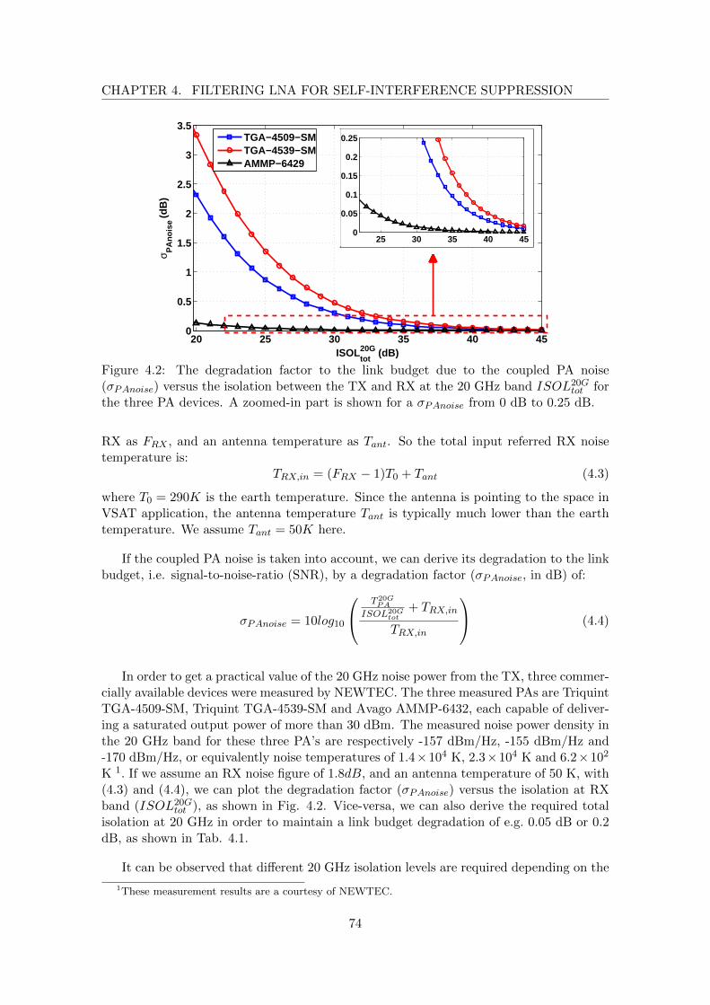
CHAPTER 4. FILTERING LNA FOR SELF-INTERFERENCE SUPPRESSION
20 25 30 35 40 450
0.5
1
1.5
2
2.5
3
3.5
ISOLtot20G (dB)
σ PA
nois
e (
dB)
TGA−4509−SMTGA−4539−SMAMMP−6429
25 30 35 40 450
0.05
0.1
0.15
0.2
0.25
Figure 4.2: The degradation factor to the link budget due to the coupled PA noise(σPAnoise) versus the isolation between the TX and RX at the 20 GHz band ISOL20G
tot forthe three PA devices. A zoomed-in part is shown for a σPAnoise from 0 dB to 0.25 dB.
RX as FRX , and an antenna temperature as Tant. So the total input referred RX noisetemperature is:
TRX,in = (FRX − 1)T0 + Tant (4.3)
where T0 = 290K is the earth temperature. Since the antenna is pointing to the space inVSAT application, the antenna temperature Tant is typically much lower than the earthtemperature. We assume Tant = 50K here.
If the coupled PA noise is taken into account, we can derive its degradation to the linkbudget, i.e. signal-to-noise-ratio (SNR), by a degradation factor (σPAnoise, in dB) of:
σPAnoise = 10log10
T 20GPA
ISOL20Gtot
+ TRX,in
TRX,in
(4.4)
In order to get a practical value of the 20 GHz noise power from the TX, three commer-cially available devices were measured by NEWTEC. The three measured PAs are TriquintTGA-4509-SM, Triquint TGA-4539-SM and Avago AMMP-6432, each capable of deliver-ing a saturated output power of more than 30 dBm. The measured noise power density inthe 20 GHz band for these three PA’s are respectively -157 dBm/Hz, -155 dBm/Hz and-170 dBm/Hz, or equivalently noise temperatures of 1.4×10⁴ K, 2.3×10⁴ K and 6.2×10²
K 1. If we assume an RX noise figure of 1.8dB, and an antenna temperature of 50 K, with(4.3) and (4.4), we can plot the degradation factor (σPAnoise) versus the isolation at RXband (ISOL20G
tot ), as shown in Fig. 4.2. Vice-versa, we can also derive the required totalisolation at 20 GHz in order to maintain a link budget degradation of e.g. 0.05 dB or 0.2dB, as shown in Tab. 4.1.
It can be observed that different 20 GHz isolation levels are required depending on the
1These measurement results are a courtesy of NEWTEC.
74
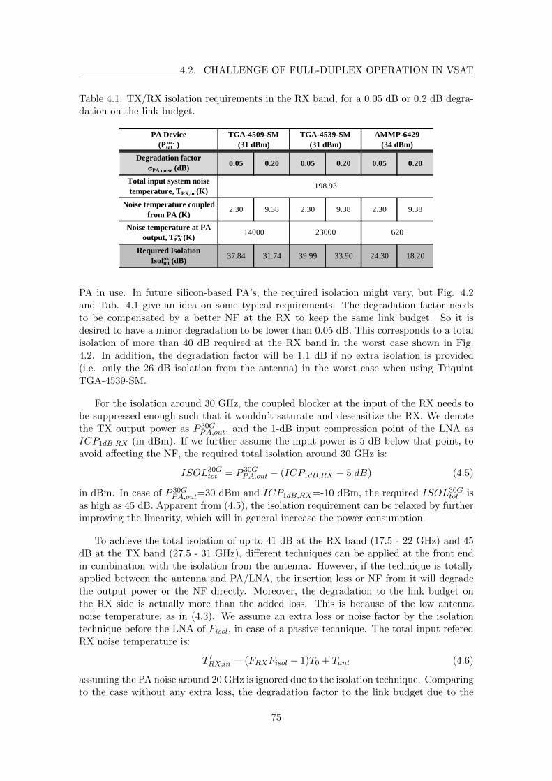
4.2. CHALLENGE OF FULL-DUPLEX OPERATION IN VSAT
Table 4.1: TX/RX isolation requirements in the RX band, for a 0.05 dB or 0.2 dB degra-dation on the link budget.
PA Device(Psat )
Degradation factorσPA noise (dB) 0.05 0.20 0.05 0.20 0.05 0.20
Total input system noise temperature, TRX,in (K)
Noise temperature coupled from PA (K)
2.30 9.38 2.30 9.38 2.30 9.38
Noise temperature at PA output, TPA (K)
Required IsolationIsoltot (dB)
37.84 31.74 39.99 33.90 24.30 18.20
TGA-4509-SM(31 dBm)
TGA-4539-SM(31 dBm)
AMMP-6429(34 dBm)
198.93
14000 23000 620
20G
20G
30G
PA in use. In future silicon-based PA’s, the required isolation might vary, but Fig. 4.2and Tab. 4.1 give an idea on some typical requirements. The degradation factor needsto be compensated by a better NF at the RX to keep the same link budget. So it isdesired to have a minor degradation to be lower than 0.05 dB. This corresponds to a totalisolation of more than 40 dB required at the RX band in the worst case shown in Fig.4.2. In addition, the degradation factor will be 1.1 dB if no extra isolation is provided(i.e. only the 26 dB isolation from the antenna) in the worst case when using TriquintTGA-4539-SM.
For the isolation around 30 GHz, the coupled blocker at the input of the RX needs tobe suppressed enough such that it wouldn’t saturate and desensitize the RX. We denotethe TX output power as P 30G
PA,out, and the 1-dB input compression point of the LNA asICP1dB,RX (in dBm). If we further assume the input power is 5 dB below that point, toavoid affecting the NF, the required total isolation around 30 GHz is:
ISOL30Gtot = P 30G
PA,out − (ICP1dB,RX − 5 dB) (4.5)
in dBm. In case of P 30GPA,out=30 dBm and ICP1dB,RX=-10 dBm, the required ISOL30G
tot isas high as 45 dB. Apparent from (4.5), the isolation requirement can be relaxed by furtherimproving the linearity, which will in general increase the power consumption.
To achieve the total isolation of up to 41 dB at the RX band (17.5 - 22 GHz) and 45dB at the TX band (27.5 - 31 GHz), different techniques can be applied at the front endin combination with the isolation from the antenna. However, if the technique is totallyapplied between the antenna and PA/LNA, the insertion loss or NF from it will degradethe output power or the NF directly. Moreover, the degradation to the link budget onthe RX side is actually more than the added loss. This is because of the low antennanoise temperature, as in (4.3). We assume an extra loss or noise factor by the isolationtechnique before the LNA of Fisol, in case of a passive technique. The total input referedRX noise temperature is:
T ′RX,in = (FRXFisol − 1)T0 + Tant (4.6)
assuming the PA noise around 20 GHz is ignored due to the isolation technique. Comparingto the case without any extra loss, the degradation factor to the link budget due to the
75

CHAPTER 4. FILTERING LNA FOR SELF-INTERFERENCE SUPPRESSION
0 0.2 0.4 0.6 0.8 1 1.2 1.4 1.6 1.8 20
0.5
1
1.5
2
2.5
3
3.5
4
NFisol
, in dB
dB
Degradation factor σisol
Figure 4.3: Degradation factor σisol to the link budget due to the extra noise figure fromthe isolation technique.
extra NF can be derived as:
σisol = 20log
((FRXFisol − 1)T0 + Tant
(FRX − 1)T0 + Tant
)(4.7)
When Tant = T0, σisol equals the extra noise figure. However, when Tant = 50 K, σisolis more than this ’dB-per-dB’ rule. As plotted in Fig. 4.3., the extra NFisol will give adegradation on link budget by almost twice of NFisol in dB.
In conclusion, the challenge in a full-duplex operation is to achieve a high total isolationwhile maintaining a low loss or low NF. Similar levels of isolation are required around theRX band and TX band. In this chapter, we will focus on isolating the blocker around 27.5- 31 GHz at the RX input, i.e. ISOL30G. The target is to achieve a high attenuation inorder to tolerate the large leakage power from the 30 dBm transmitted power, meanwhilemaintaining a total LNA NF of lower than 2 dB. In the next section, we will first reviewthe state-of-the-art 20 GHz LNA’s and introduce some potential filtering or cancellationtechniques.
4.3 Literature Review
As explained in the introduction, the VSAT application typically has critical requirements,especially on the receiver noise figure (NF), which is traditionally realized using III-Vcompound technologies. Such technologies can achieve a low NF below 2 dB [65] at K/Ka-band. Recently, comparable NF has been demonstrated in silicon-based technologies,which can offer lower cost and higher integration [61, 62, 63]. Sub 2 dB NF are achievedin CMOS-SOI and SiGe BiCMOS technologies at the K/Ka-band.
However, silicon technologies still suffer from higher loss from passive devices thancompound technologies. An on-chip 3-rd order bandpass filter [60] implemented in BiC-MOS technology has a loss of more than 5.1 dB from 23.4 GHz to 31.0 GHz. For our
76

4.4. DESIGN DESCRIPTION
isolation purpose, using passive filtering completely at the input of a LNA is difficult asvery low loss and high filtering attenuation are required at the same time.
An alternative is to use an active notch filter. In [66], a dual-band LNA with twoactive notch filters achieves about 23 dB attenuation (compared to the gain at pass-band)at 30 GHz. However, the filtering is narrow-band and it can have linearity issues in caseof high power blockers due to the non-linear properties of the active devices.
Another active approach is feed-forward cancelling (FFC), such as in [67, 68]. Given thefact that the TX and RX are co-located, the FFC technique couples part of the TX signaland couples it back at the RX input after tuning it to an anti-phase copy of the leakageTX signal. In order to have low loss, the coupling factor needs to be low, which requires avery high power operation in the FFC path. It increases significantly the complexity andpower consumption. Besides the FFC can also add uncorrelated noise from the cancelingpath.
In this work, passive filtering will be used, due to the high TX power in the VSATapplication. In order to minimize the additional loss and achieve a total NF of less than2 dB, the filter is co-designed with the LNA. The design details are presented in the nextsection.
4.4 Design Description
4.4.1 Trade-off Between Filtering and Noise Figure Degradation
To prevent the leakage transmitter signal from desensitizing and saturating the LNA, notchfilters at 30 GHz can be implemented at the input. In general, higher order filtering willinduce higher pass-band insertion loss, which poses a direct trade-off between the filteringand noise figure degradation. To relax this direct trade-off, we propose to implementnotch filters with lower order at different stages of the LNA. Initial filtering at the input isnecessary to avoid the input transistor already being saturated and desensitized. Typically,the input transistor with degeneration doesn’t provide much transducer gain, since it isgenerally optimized for low NF and the stages afterwards provide most of the gain. As aresult, the input filtering is more relaxed and most of the filtering can be done after theinput transistor. In addition, the input filter can be part of the input matching to furtherreduce its impact on the NF. Due to the available gain from the first transistor, loss fromthe following filters has less contribution to the total NF.
To illustrate this consideration more quantitatively, we can calculate the total NF andinput compression point of the simplified cascaded amplifier with filters between each stageshown in Fig. 4.4. In this generalized and simplified model, we assume a 3-stage amplifier,with notch filter at the input and between stages. The notch filters have loss of L20G
i at 20GHz and attenuation of Att30G
i at 30 GHz, for i = 1, 2, 3. All the performance parametersof each block are listed below in Fig. 4.4. All the parameters are in linear scale.
Further assumptions are made on the G30Gi and L20G
i . We assume each amplifier hasa peak gain at 20 GHz with a roll-off factor of two (Rf = 2) at 30 GHz (e.g. due to
77

CHAPTER 4. FILTERING LNA FOR SELF-INTERFERENCE SUPPRESSION
201
201
301
301
G
G
G
G
G
F
G
ICP
201
201
301
G
G
G
L
L
Att
202
202
302
G
G
G
L
L
Att
203
203
302
G
G
G
L
L
Att
202
202
302
302
G
G
G
G
G
F
G
ICP
203
203
303
303
G
G
G
G
G
F
G
ICP
Gain (G) or Loss (L)
@ 20 GHz:
NF @ 20 GHz:
Gain (G) or Attenuation (Att)
@ 30 GHz:
Input Compression Point
@ 30 GHz:
Filter 1 Amp 1 Filter 2 Amp 2 Filter3 Amp 3
Figure 4.4: Simplified model of a 3-stage amplifier with notch filters at each stage. Allthe parameters are in linear scale.The unit of input compression point is mW. Lower scoredenotes the number of the component and upper score denotes the frequency that theparameter indicates.
matching). This means that, if there is no filter, the total gain at 30 GHz from threestages is 9 dB lower than the 20 GHz gain. Besides, we assume a scalable L20G
i withAtt30G
i :Att30G
i |dB = γ · L20Gi |dB (4.8)
where γ is a scalar with an assumed value of 20. This means 20 dB of attenuation at30 GHz from the filter will contribute 1 dB loss at 20 GHz. The scalability comes fromthe fact that we can cascade more stages of filters to have more attenuation at the stopband which also increases loss (in dB) proportionally. The value of γ is dependent on thequality factor of the filter and the frequency separation. The use of it can simplify theanalysis here.
Using Friis formula, we could derive the total noise factor (F 20Gtot ) at 20 GHz as:
F 20Gtot = L20G
1 · F 20G1 +
(L20G2 · F 20G
2 − 1) · L20G1
G20G1
+(L20G
3 · F 20G3 − 1) · L20G
1 · L20G2
G20G1 G20G
2
(4.9)
For the input compression point with respect to 30 GHz signals, we can view Filter iand the amplifier after it Amp i as one component, and the input compression point isimproved from ICP 30G
i to ICP 30Gi · Att30G
i for i = 1, 2, 3. Similarly, we can derive thetotal input compression point at 30 GHz as:
ICP 30Gtot =
1
ICP 30G1 ·Att30G
1
+
G20G1
RfAtt30G1
ICP 30G2 ·Att30G
2
+
G20G1
RfAtt30G1
G20G2
RfAtt30G2
ICP 30G3 ·Att30G
3
−1
(4.10)
The assumed values of the parameters in Fig. 4.4 are summarized below:
• G20G1 |dB = 8 dB, G20G
2 |dB = 8 dB, G20G3 |dB = 12 dB.
78

4.4. DESIGN DESCRIPTION
Att230G (dB)
Att
130G
(d
B)
0 5 10 15 20 250
5
10
15
20
25
20 dBm
10 dBm
5 dBm
0 dBm
: NFtot20G
: ICPtot30G
25 dBm
2.4 dB
2.2 dB
2.0 dB
1.8 dB
1.6 dB
1.4 dB
15 dBm
Figure 4.5: The contour plot of F 20Gtot (dotted contour) and ICP 30G
tot (solid contour) versusAtt30G
1 |dB and Att30G2 |dB.
• NF 20G1 = 0.9 dB, NF 20G
2 = 1.2 dB, NF 20G3 = 2 dB.
• ICP 30G1 |dBm = 2 dBm, ICP 30G
2 |dBm = 2 dBm, ICP 30G3 |dBm = 6 dBm.
If the total attenuation from the 3 filters is assumed to be 40 dB, i.e. Att30G1 |dB +
Att30G2 |dB + Att30G
3 |dB = 40 dB, we can plot the contour of F 20Gtot and ICP 30G
tot versusAtt30G
1 |dB and Att30G2 |dB, as shown in Fig. 4.5. The dashed contour lines are the resulted
NF 20Gtot (in dB) and solid curved contour lines are the ICP 30G
tot (in dBm). A bounded linecan be observed at the top right, due to the constraint equation Att30G
1 |dB +Att30G2 |dB +
Att30G3 |dB = 40 dB.
The first observation is that if there is no filtering at all for Att30G1 |dB and Att30G
2 |dB,the compression point against 30 GHz blocker is about -5 dBm. When the TX power is30 dBm, and the coupling between TX and RX antenna is -26 dB, this compression pointshould be better than 9 dBm with 5 dB margin. If no filtering is implemented at stage2, i.e. Att30G
2 |dB = 0 dB, we need Att30G1 |dB of about 14 dB (while Att30G
1 |dB = 26 dB)to reach the 9 dBm ICP 30G
tot , and the NF 20Gtot is about 1.9 dB. It is close to the 2 dB
requirement, leaving no margin for the layout degradation.
79

CHAPTER 4. FILTERING LNA FOR SELF-INTERFERENCE SUPPRESSION
iin
ZL ZL
vin
(a) (b)
L
CL
C
Figure 4.6: Simple series or parallel LC resonance filters. (a) Series notch filter, (b) Parallelnotch filter.
Table 4.2: Simple series or parallel LC resonance, and their effective inductance or capac-itance above or below the resonance frequency fres. Z(fres) is the effective impedance atfres.
Capacitive: Inductive:
Inductive: Capacitive:
1
1
∙ 1
∙ 1
1
2
0
1
2
∞
This can be relaxed by applying filtering at the second stage. From this illustrationplot, we can observe the we can actually distribute the levels of filtering by Att30G
1 andAtt30G
2 to achieve a lower noise figure while keeping on the same contour level of ICP 30Gtot .
If the desired ICP 30Gtot is at least 9 dBm, the optimum values of Att30G
1 and Att30G2 in this
case are around 8 dB and 12 dB respectively, as denoted in the dashed circle in Fig. 4.5.In this case, the NF 20G
tot can be improved by 0.2 dB compared to the case when Att30G2 |dB
= 0 dB. Although the overall filtering and loss from Att30G1 |dB and Att30G
2 |dB is higher,the resulted total noise figure is even better for the same ICP 30G
tot level. Besides, we canalso notice that, for a certain level of Att30G
1 |dB, as Att30G2 |dB increases, the ICP 30G
tot willincrease and saturate to a certain level, because the limited linearity of the first stage willdominate.
In Section 4.4.3, we will use this strategy in the filtering LNA design to achieve a lownoise figure at 30 GHz while with 30 GHz blocker tolerance.
4.4.2 Series or Parallel LC Resonance Filter
Other than optimizing the level of filtering at different stages, further reducing the impacton NF can be achieved by co-designing the filtering and matching.
80

4.4. DESIGN DESCRIPTION
In general, a simple filter is prefered given that it provides a good filtering property,especially for the filter at the input which directly gives rise to the total NF. In our case, thesimplest form of filter can be a resonant type notch filter. For example, a shunt capacitorin series with an inductor can provide a low impedance at the resonance frequency fres asin Fig. 4.6(a), or an inductor and a capacitor in parallel gives a high impedance at fresas in Fig. 4.6(b).
Meanwhile, at frequencies other than fres they can be viewed effectively as a capacitoror an inductor. Take the series LC in Fig. 4.6(a) as an example, it is as an inductor shuntto the ground for frequencies higher than fres, and as a shunt capacitor for frequencieslower. We can derive the narrow-band effective capacitance or inductance values for theseries and parallel LC resonance as listed in Tab. 4.2. This actually can be utilized toobtain matching for different frequencies. For example in Fig. 4.6(b), it can be used atthe input of an LNA as a notch filter at 30 GHz, while it acts as a series inductance for(part of) the input matching.
However, this simple LC resonance filters in Tab. 4.2 only provide limited possibilities.For cases when the matching frequency is lower than the notch frequency (fres), only thefirst column in Tab. 4.2 is useful, which only gives the possibility of a shunt capacitance ora series inductance for matching purpose. Similarly, when the matching frequency is higherthan the notch frequency (fres), only the last column in Tab. 4.2 is useful. Actually, wecan extend the resonance filters by adding one more component (L
′or C
′). We conclude
the general properties of the effective reactances of the three-component resonant notchfilters in Appendix C for reference. In the following design, only the simple LC paralleland series resonances in Tab. 4.2 is used, because they can already provide the desiredmatching at the critical locations in the design described in the next section, and becauseit is not necessary to add the complexity which also increases loss and chip area.
4.4.3 Filtering Low Noise Amplifier Design
The schematic of a single-ended filtering LNA is shown in Fig. 4.7. The LNA consistsof a cascode stage followed by a common emitter output stage. Three-stage filterings areimplemented in the LNA.
In order to have low NF, the input matching and filtering at the input needs to bedesigned carefully. First, the input transistor is biased at the optimum current density forthe minimum NF (Jopt = 2.3mA/µm2) at 20 GHz. The transistor size is scaled to have thereal part of the optimal noise impedance (Ropt = Real(Zopt)) to around 50 Ω, as shown inFig. 4.8. The degeneration inductor (Le1) at the emitter is selected in order to have thereal part of the input impedance seen into the base (R
′in = Real(Z
′in)) to around 50 Ω,
while not influencing the Zopt much. A series ind uctance at the input can then achievea simultaneous noise and power matching. This simplifies the input matching with lessloss. In this design, transistor Q1 has a total length of 20 µm with the minimum widthof 0.3 µm from the technology, with a biasing current of 13.7 mA. The biasing is simplyprovided by a base voltage for the common-emitter transistors in this test chip design.
To implement the input filter with minimum impact on the NF, a parallel LC (Lf1 of169 pH and Cf1 of 165 fF) lumped filter is added in series at the input which resonates
81

CHAPTER 4. FILTERING LNA FOR SELF-INTERFERENCE SUPPRESSION
Q1
Q2 Q3
Q1: 0.3µm xxxx 4µm xxxx 5Q2: 0.3µm xxxx 14µm xxxx 5Q3: 0.3µm xxxx 12µm xxxx 7
L f1=169 pH
Cf1=165 fF
L f2=49 pHCf2=560 fF
L c1=210 pH
Cc1=130 fFL f4=50 pH
Cf4=620 fFCf3=100 fF
L f3=290 pH
L c2=630 pH
L e1=65 pH
L e2=60 pH
Cc2=600 fF
L b1=30 pH
Z ’opt Z ’
in
Figure 4.7: Schematic of the two-stage 20 GHz LNA’s with 30 GHz notch filters.
at fres = 30 GHz. It can have an attenuation of about 10 dB around the notch frequencyfrom 27.5 GHz to 31 GHz. Meanwhile, it acts as a series inductance around 20 GHz, asexplained in the previous section. The combination of Lf1 and Cf1 creates an effectiveinductance of about 304 pH. It provides the main part of the input matching inductancewhich only needs an extra small inductor (Lb1) of 30 pH in this design. In this way, thisvery simple input matching is adopted to provide 10 dB of filtering around 30 GHz andan optimum noise matching at the same time.
The second filter is implemented right before the cascode transistor (Q2). A highQ resonance is selected due to the small impedance seen looking into the common basetransistor Q2. Between the first and second stage, further notch filtering is done by ashunt series LC (Lf3 and Cf3) and a series parallel LC filter (Lf4 and Cf4). This providesmost of the overall filtering, and avoids the output stage being compressed too soon. Atthe output stage, a common emitter amplifier is used to provide sufficient gain with goodlinearity. Furthermore, a high voltage transistor is used for the output stage to improvelinearity.
4.4.4 Reference Low Noise Amplifier Design without Filtering
In order to compare the filtering performance and the noise figure degradation due tofiltering, an LNA without filters is also designed as a reference LNA. It excludes all thefilters, as shown in Fig. 4.9. In order to have a fair comparison, the matchings are re-tunedaccordingly for its optimum performance, especially in terms of noise figure and gain. Inthis reference LNA, the input transistor Q1 is scaled to a larger size (total length of 25 µm),which results in a lower real part in the optimum noise impedance (Real(Zopt)). Shown inFig. 4.10, a shunt inductor can then be used for simultaneous noise and power matching
82

4.4. DESIGN DESCRIPTION
0.2
0.5
1.0
2.0
5.0
+j0.2
−j0.2
+j0.5
−j0.5
+j1.0
−j1.0
+j2.0
−j2.0
+j5.0
−j5.0
0.0 ∞
Z’in
Zin
Le
Z’opt
, NFmin
=1.08 dB
Zopt
, NFmin
=1.0 dB
Figure 4.8: Input stage design for gain and NF matching for the filtering LNA. Zopt is theoptimum source impedance for minimum NF, and Zin is input impedance seen into thetransistor Q1. They are changed to Z
′opt and Z
′in with the degeneration inductor Le.
in this case, and it gives a better overall NF. Furthermore, the required degenerationinductance (Le) has a smaller value than in Fig. 4.8, which also helps slightly for reducingthe NF.
One may consider to use this scaled-up transistor for the input in the filtering LNA.The required shunt inductance can be implemented using filter ¬ or ¯ in Fig. C.1 inAPPENDIX C. However, due to the higher loss from the extra inductor which leads to aNF higher than 2 dB, it is not used in this design.
The second stage is the same for the reference LNA, and the output matching is similaras for the filtering LNA.
4.4.5 Layout Design
The two LNAs are designed and fabricated in a 0.25µm SiGe:C BiCMOS technology whichfeatures peak ft/fmax of 216/177 GHz [69] and a minimum NF of about 0.9 dB at 20 GHz.A full-custom layout is realized for optimized performance. The whole layout including
83

CHAPTER 4. FILTERING LNA FOR SELF-INTERFERENCE SUPPRESSION
Q1
Q2Q3
L b1=730 pHLe1=40 pH
L c1=244 pH
L b2=80 pH
Cc1=160 fF
L c2=690 pH
Le2=60 pH
Cc2=400 fF
Q1: 0.3µm xxxx 5µm xxxx 5Q2: 0.3µm xxxx 10µm xxxx 5Q3: 0.3µm xxxx 12µm xxxx 7
Figure 4.9: Schematics of the reference two-stage 20 GHz LNA’s without filters.
probe pads is simulated and optimized in ADS Momentum [53]. The layout of the filteringLNA is shown in Fig. 4.11. A ground plane at the top metal layer surrounding the passivedevices is implemented throughout the chip to provide a good ground reference in thesingle-ended design. The ground plane also provides a well defined path for the returncurrent. The inductors use the top two metals stacked together to have a better qualityfactor. The input transistor is placed as close to the input pad as possible to reduce NFdegradation. The distance between the transistors is kept with some distance, so that theinductors are not close to each other in order to have lower coupling between the inductors.The inevitable connection lines (acting as transmission lines) are taken into account in theEM simulations.
4.5 Simulation and Measurement Results
The fabricated chip micrograph is shown in Fig. 4.12. The two LNA’s occupy about 660µm× 780 µm each including pads. The measured power consumptions of the filtering LNAand the reference LNA are 87.5 mW and 92.5 mW respectively under a 2.5 V supply.
The measured |S21| is shown in Fig. 4.13. The filtering LNA achieves a |S21| of 24.3dB at 20 GHz. It is about 3 dB lower than the gain of the non-filtering LNA, which is27.4 dB. The 3-dB gain bandwidths are about 4.3 GHz and 5 GHz respectively for thetwo LNA’s.
At the TX band 27.5 GHz to 31 GHz, there is 17.5 dB to 15.2 dB gain for the LNAwithout any filtering. For the LNA with filtering, the gain at this frequency range isreduced to -12.9 dB and -18.5 dB at the two edge frequencies, namely a total attenuationof more than 30 dB. Between 28.5 and 29.5 GHz an attenuation of more than 45dB isachieved.
84

4.5. SIMULATION AND MEASUREMENT RESULTS
0.2
0.5
1.0
2.0
5.0
+j0.2
−j0.2
+j0.5
−j0.5
+j1.0
−j1.0
+j2.0
−j2.0
+j5.0
−j5.0
0.0 ∞
Le
Zopt
, NFmin
=1.0 dB
Z’opt
, NFmin
=1.04 dB
Zin
Z’in
Figure 4.10: Input stage design for gain and NF matching for the reference LNA withoutfilters. Zopt is the optimum source impedance for minimum NF, and Zin is input impedanceseen into the transistor Q1. They are changed to Z
′opt and Z
′in with the degeneration
inductor Le.
The measured minimum NF of the filtering LNA is about 1.9 dB, as shown in Fig.4.14, while it is 1.8 dB for the non-filtering version. At 22 GHz, the filtering LNA’s NFraises up to about 2.3 dB, which is 0.4 dB higher than the non-filtering version.
The reflection coefficients are plotted in Fig. 4.15. Some deviation between simulationand measurement can be observed on the |S11| of the filtering LNA, which is due tosimulation inaccuracies on the substrate. The input 1-dB compression point (ICP 20G
1dB )and the input third-order intercept point (IIP3) of the filtering LNA is -11.7 dBm and -0.5dBm respectively, while -14.5 dBm and -2.5 dBm for the non-filtering LNA.
To verify the linearity performance in presence of a large blocker around 30 GHz, gaincompression and triple-beat (TB) intermodulation distortion [25] are measured. As shownin Fig. 4.16, in the worst case, the gain of the filtering LNA at 20 GHz is compressed by1 dB when there is a 28.5 GHz blocker at about 6 dBm, whereas the ICP 30G
1dB is around-11 dBm for the non-filtering LNA. This corresponds to an improvement of more than 17dB for gain compression.
85

CHAPTER 4. FILTERING LNA FOR SELF-INTERFERENCE SUPPRESSION
Lf1
Lb1
Cf1
Q1
Q2
Q3
Lf2Cf2
Lc1
Lf3
Lf4
Le1 Le2
Lc2
in out
Figure 4.11: The layout of the filtering LNA.
660 m 660 m
780 m
Figure 4.12: Die photo of the LNA’s with (left) and without (right) filtering.
Another measurement on the linearity in presence of large blockers is the TB measure-ment. In this measurement, three tones are present at the input, as shown in Fig. 4.17.
86

4.5. SIMULATION AND MEASUREMENT RESULTS
15 20 25 30 35−50
−40
−30
−20
−10
0
10
20
30
Frequency (GHz)
S21
(dB
)
With filtering
RX band TX band
Without filtering
Figure 4.13: Simulated (dashed lines) and measured (symbolled lines) S21 of the LNA’swith and without filtering.
17 18 19 20 21 22
1.5
2
2.5
3
Frequency (GHz)
NF
(d
B)
simulated, without filteringsimulated, with filteringmeasured, without filteringmeasured, with filtering
Figure 4.14: Simulated and measured NF of the LNA’s with and without filtering.
The two tones around 30 GHz Pblk1 and Pblk2 represent a modulated leakage signal fromthe TX. If a 20 GHz signal is received, two 3rd-order distortion products will be generatedaround the 20 GHz tone. The level of the TB1 and TB2 tones with respect to the 20 GHz
87

CHAPTER 4. FILTERING LNA FOR SELF-INTERFERENCE SUPPRESSION
15 20 25 30−30
−25
−20
−15
−10
−5
0
Frequency (GHz)
S11
(dB
)
with filtering
without Filtering
(a)
15 20 25 30−30
−25
−20
−15
−10
−5
0
Frequency (GHz)
S22
(dB
)
with filtering
without filtering
(b)
Figure 4.15: Simulated (dashed lines) and measured (symbolled lines) S11 and S22 of theLNA’s with and without filtering.
−30 −25 −20 −15 −10 −5 0 5 10 15−2
−1.5
−1
−0.5
0
fblk
(GHz)
∆Gain(dB)
fblk
= 27.5 GHz
fblk
= 28 GHz
fblk
= 28.5 GHz
fblk
= 29 GHz
fblk
= 29.5 GHz
fblk
= 30 GHz
fblk
= 30.5 GHz
fblk
= 31 GHz
without Filtering
with Filtering
Figure 4.16: Gain compression at 20 GHz versus power level of the blockers from 27.5GHz to 31 GHz.
tone is defined as triple beat ratio (TBR), in dBc. Similar as IIP3 definition, we definethe TBIIP3 (in dBm) as:
TBIIP3 = Pblk +TBR
2(4.11)
where Pblk (in dBm) is the power of the two blocker tones. The TBIIP3 actually represents
88

4.5. SIMULATION AND MEASUREMENT RESULTS
Pblk1
30GHz
PRX
20GHz
Pblk2
∆f
TB1 TB2TBR
∆f
Figure 4.17: Triple beat (TB) test in presence of large blocker signals at 30 GHz.
Without Filtering
With Filtering
Figure 4.18: Measured spectrums from the triple beat measurement on the two LNA’s.fblk = 30 GHz, ∆f = 50 MHz, Pblk = −10 dBm for the non-filtering LNA and Pblk = 10dBm for the filtering LNA.
the extrapolated level of the blocker tones when the TB’s have the same power as the 20GHz tone.
For the TBIIP3 measurement, two tones around 30 GHz with a spacing of 50 MHzare applied at the input with a single-tone jammer at 20 GHz, and the cross-modulationproducts at ± 50 MHz offset around 20 GHz are measured. The two-tone blockers are -10dBm and 10 dBm at the input for the LNA’s with and without filtering respectively. Asshown in Fig. 4.18, the TBR is 17.8 dBc and 26.0 dBc, corresponding to a TBIIP3 of -1.1dBm and 23.0 dBm for the two LNA’s respectively. The ICP1dB,blk and TBIIP3 versusblocker frequencies from 27.5 GHz to 30 GHz is shown in Fig. 4.19 according to (4.11).
89

CHAPTER 4. FILTERING LNA FOR SELF-INTERFERENCE SUPPRESSION
27.5 28 28.5 29 29.5 30 30.5 31−20
0
20
40
fblk
(GHz)
dBm
Input compression point, and TB IIP3
ICP1dB, with filtering
TB IIP3, without filtering
ICP1dB, without filtering
TB IIP3, with filtering
Figure 4.19: The 1 dB input gain compression point and TBIIP3 due to the presence oflarge blocker at fblk.
We can refer back the measurement results to the discussion on the VSAT requirementsin section 4.2. In a VSAT scenario, a TX signal in the range 27.5 - 31 GHz will reachat the filtering LNA input with a power of 4 dBm (assuming the antenna coupling of -26dB). It is about 2 dB lower than the ICP1dB,blk in the worst case (when the blocker isaround 28.5 GHz). And it is more then 9 dB lower than the ICP1dB,blk at 30 GHz. Asshown in Fig. 4.16, the total gain is compressed by less than 0.5 dB in presence of the 4dBm blocker at the filtering LNA input, while the gain is compressed by far more than 2dB for the reference LNA.
For the 3rd-order distortion due to this 4 dBm coupled blocker, from (4.11), we cancalculate that the TBR is 27 dB in the worst case, i.e. the distortion product is morethan 27 dB lower than the desired signal at 20 GHz. In case of adjacent channel inter-ference in the 20 GHz band from other communication links, significant degradation tothe SINR might occur if the adjacent channel has a much higher power comparing to thedesired signal. This adjacent channel problem can be mitigated by frequency planning,e.g. adopting larger guard bands between carriers [70], and is not within the scope of thiswork.
4.6 Benchmarking and Performance Summary
Tab. 4.3 summarizes the performance and benchmarks of recent LNA’s around 20 GHz[65, 71, 63, 72, 61], and a filtering LNA [66]. For the LNA performance around 20 GHz,both LNA’s in this work demonstrate lowest NF at K-band in silicon and with high overallperformance in terms of the figure-of-merit. Moreover, the filtering LNA demonstrates alow NF around 20 GHz and high attenuation across the 27.5 - 31 GHz band, comparingto the other LNA with active notch filters. And the filtering LNA demonstrates highlinearity performance in presence of a block in the frequency range between 27.5 and 31GHz.
In the last two columns in Tab. 4.3, the performance of two commercially availablewaveguide filters [73, 74] are summarized assuming they are integrated with the non-filtering LNA chip designed in this chapter. The waveguide bandpass filter Model 18810
90
4.6. BENCHMARKING AND PERFORMANCE SUMMARY
[73] from Microwave Filter Company, Inc. has a passband between 18.3 GHz to 22 GHzwith a loss of 0.75 dB (typical value), and for frequencies above 24 GHz it has a rejectionof more than 30 dB. If we place this filter in front our non-filtering LNA, it can achievea better blocker tolerance than our filtering LNA design. However, the NF is over 2 dB,when the loss from the interface between chip and waveguide is not yet considered. Whenthe band reject filter Model 18811 [74] is used, which is dedicated to reject the TX bandfrom 27.5 GHz to 31 GHz, very deep rejection can be achieved with a low loss. When anideal interface is assumed, the achieved total NF is similar as our filter LNA design.
In summary, for scenarios when much higher isolation is required, e.g. when TX poweris significantly higher or the antenna isolation is low, the waveguide filters are still morecompetitive in terms of performance. For our case, the on-chip filtering LNA in thischapter can provide the required tolerance against 30 GHz blocker, with minimal impacton the total NF. It can be a compact and integrated solution for the VSAT full-duplexoperation.
91
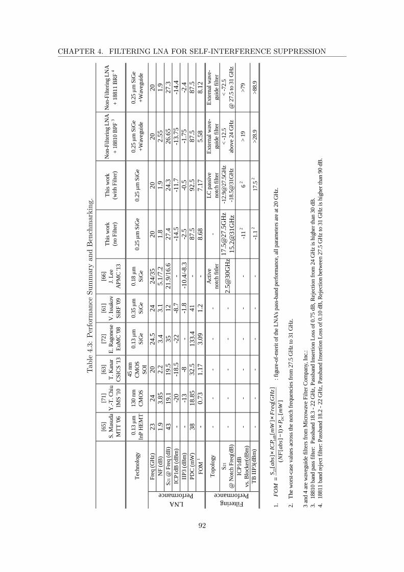
CHAPTER 4. FILTERING LNA FOR SELF-INTERFERENCE SUPPRESSION
Tab
le4.
3:P
erfo
rman
ceS
um
mar
yan
dB
ench
mar
kin
g.
[65]
S. M
asud
aM
TT
'06
[71]
Y.-
T. C
hiu
IMS
'10
[63]
T. K
anar
CS
ICS
'13
[72]
E. R
agon
ese
EuM
C '0
8
[61]
V. I
ssak
ovS
iRF
'09
[66]
J. L
ee
AP
MC
'13
Thi
s w
ork
(no
Filt
er)
Thi
s w
ork
(with
Filt
er)
Non
-Filt
erin
g LN
A+
188
10 B
PF
3N
on-F
ilte
ring
LNA
+ 1
8811
BR
F 4
Te
chno
logy
0.1
3 µm
InP
HE
MT
130
nmC
MO
S
45 n
mC
MO
S
SO
I
0.13
µm
SiG
e0.
35 µ
mS
iGe
0.18
µm
SiG
e0.
25 µ
m S
iGe
0.25
µm S
iGe
0.25
µm
SiG
e+
Wav
egu
ide
0.25
µm
SiG
e+
Wav
egu
ide
Fre
q (G
Hz)
23
24
20
24
.52
42
4/3
52
02
02
02
0N
F (
dB)
1.9
3.8
52
.23
.43
.15
.1/7
.21
.81
.92
.55
1.9
S21
@ F
req
(dB
)4
31
9.1
19
.53
51
22
1.9
/16
.62
7.4
24
.32
6.6
52
7.3
ICP
1dB
(dB
m)
--2
0-1
8.5
-22
-8.7
--1
4.5
-11
.7-1
3.7
5-1
4.4
IIP
3 (d
Bm
)-
-13
-8-
-1.8
\-10
.4/-
8.3
-2.5
-0.5
-1.7
5-2
.4P
DC
(m
W)
38
18
.85
32
.51
33
.44
1-
87
.59
2.5
87
.58
7.5
FO
M 1
-0
.73
1.1
73
.09
1.2
-8
.68
7.1
75
.58
8.1
2
Top
olog
y-
--
--
Act
ive
notc
h fit
ler
-LC
pas
sive
no
tch
filte
rE
xte
rnal
wav
e-
guid
e fi
lter
Ext
ern
al w
ave
-gu
ide
filte
rS2
1
@ N
otch
Fre
q(dB
)-
--
--
2.5
@3
0G
Hz1
7.5
@2
7.5
GH
z1
5.2
@3
1G
Hz
\-12
.9@
27.5
GH
z-1
8.5@
31G
Hz
< -
12.5
abov
e 2
4 G
Hz
< -
72.5
@ 2
7.5
to 3
1 G
Hz
ICP
1dB
vs
. Blo
cke
r(dB
m)
--
--
--
\-11
2\6
2>
19
>79
TB
IIP
3(dB
m)
--
--
--
\-1.
1 2
\17.
5 2
>28
.9>
88.9
LNA Performance
Filtering Performance
1.
: fig
ure
-of-
me
rit o
f the
LN
A's
pas
s-ba
nd p
erf
orm
ance
, all
para
me
te
rs a
re a
t 20
GH
z.
2.
The
wor
st-c
ase
val
ues
acro
ss th
e n
otch
fre
que
nci
es
from
27.
5 G
Hz
to 3
1 G
Hz.
3 an
d 4
are
wav
egu
ide
filte
rs fr
om M
icro
wav
e F
ilte
r C
ompa
ny, I
nc.:
3.
1881
0 ba
nd p
ass
filte
r: P
assb
and
18.3
- 2
2 G
Hz,
Pas
sban
d In
sert
ion
Loss
of 0
.75
dB, R
eje
ctio
n fr
om 2
4 G
Hz
is h
ighe
r th
an 3
0 dB
.4.
18
811
band
re
ject
filte
r: P
assb
and
18.2
- 2
2 G
Hz,
Pas
sban
d In
sert
ion
Loss
of 0
.10
dB, R
eje
ctio
n b
etw
ee
n 27
.5 G
Hz
to 3
1 G
Hz
is h
ighe
r th
an 9
0 dB
.
21
1[
][
][
]
([
]1)
[]
dB
DC
Sab
sIC
Pm
WF
req
GH
zF
OM
NF
abs
Pm
W
××
=−
×
92
4.7. SUMMARY AND CONCLUSIONS
4.7 Summary and Conclusions
In this chapter, we explained the design challenges in full-duplex operation for VSATapplication. High isolation is required in order to avoid significant degradation to the linkbudget, while the isolation technique needs to be low loss. For the isolation around the TXband, we demonstrated a 20 GHz LNA design with passive filtering fully integrated on-chipin SiGe BiCMOS 0.25 µm technology, and compared to a reference LNA without filteringin the same technology. The proposed filtering LNA adopts passive filters at differentstages to achieve high order of attenuation with minor impact on the NF. Meanwhile, theco-design of the filter and matching networks further reduces the impact on the NF fromthe added filtering function. The non-filtering LNA achieves a record NF of 1.8 dB. Thefiltering LNA achieves an attenuation of more than 30 dB from 27.5 GHz to 31 GHz witha 0.1 dB to 0.4 dB degradation on NF. It improves the linearity in presence of strongblockers by more than 17 dB for both gain compression and triple beat measurements.
The proposed filtering LNA demonstrates that it is possible to provide high isolationwith a low loss by a careful design on the on-chip passive filters and matching networks.This integrated solution can be used for future Ka-band VSAT full-duplex applications.A similar approach can be used in the PA design to filter the noise around 20 GHz.
93

CHAPTER 4. FILTERING LNA FOR SELF-INTERFERENCE SUPPRESSION
94

Chapter 5
Hybrid-Transformer BasedDuplexer for Self-InterferenceSuppression
5.1 Introduction
The previous chapter presented a filtering LNA design with high attenuation at the trans-mitter (TX) band and low noise figure at the receiver (RX) band, for the duplex operationin a VSAT application. In the targeted VSAT scenario, the frequency difference betweenthe RX and TX is relatively large (20 GHz versus 30 GHz). Another scenario is whenthe RX and TX frequencies are close to each other. In this case, passive filtering becomesvery challenging, due to the limited quality factor of the on-chip passive devices. Exam-ples of this scenario include frequency-division duplexing (FDD) communication as wellas imaging and radar applications.
In this scenario when RX and TX are close in frequency, duplexers are critical com-ponents in order to simultaneously transmit and receive while sharing the same antenna.However, signal leakage from the transmitter’s (TX’s) high power output to the receiver(RX), due to the finite TX/RX isolation, can cause saturation and desensitization in theRX. Meanwhile, low insertion loss is desired. The duplexer is located between the antennaand the transceiver front end, so its loss will directly degrade the RX’s noise figure (NF)and TX’s output power, and will therefore further deteriorate the system’s link budget.As a result, high isolation and low loss is crucial for duplexers.
This chapter focuses on exploring duplexer design at millimeter-wave frequency (mm-wave). A millimeter-wave tunable hybrid-transformer based duplexer concept with dual-antenna configuration will be presented. By using orthogonal sequentially-rotated linearly-polarized antennas and the hybrid-transformer based duplexer, the transmitter and re-ceiver duplexes the two antennas with orthogonal circular-polarized signals. An on-chiptuning technique is proposed to improve the isolation of the duplexer in case of impedanceimbalances. The on-chip duplexer is implemented in a 0.25 µm SiGe BiCMOS technology,and measurement results demonstrate an isolation of more than 45 dB by the duplexer for
95

CHAPTER 5. HYBRID-TRANSFORMER BASED DUPLEXER
a 1 GHz bandwidth. This high isolation can be tuned from 27 GHz to 34 GHz. The totalRX path’s noise figure (NF) is 4 dB and TX path’s insertion loss is 3.1 dB. An alternativeduplexer with a similar principle using an on-board rat-race coupler is also proposed anddesigned for comparison. Packaged prototype modules using the on-chip duplexer andthe rat-race coupler both integrated with on-board aperture-coupled microstrip antennaswith sequential rotation technique have been developed. Measurement results demonstratethe orthogonal circular polarizations for the RX and TX mode on both prototypes. Theachieved isolation by the on-chip tunable duplexer is better than 50 dB between 30.2 GHzand 31.2 GHz, while the achieved isolation by the rat-race version is about 20 dB in thesame bandwidth.
The chapter is organized as follows. A literature review of the state-of-the-art duplexersis presented in Section 5.2. Section 5.3 introduces the proposed dual-antenna architectures.An alternative duplexer using a rat-race coupler is introduced in Section 5.4. Section 5.5gives an overview of the 30 GHz prototype that is developed using the hybrid-transformerduplexer. The design details of the duplexer chip and the antenna board are described inSection 5.6 and Section 5.7 respectively. Measurement results are presented in Section 5.8.Section 5.9 discusses some possible extensions of the duplexer concept. Finally, Section5.10 concludes this chapter.
5.2 Literature Review
Low-loss external ferrite-based circulators are traditionally used as duplexers [75]. How-ever, they are relatively bulky, narrow-band, and the isolation is typically limited to 20dB at mm-wave frequencies [76]. Alternatively, on-chip integrated duplexers can providea compact and low-cost solution. An on-chip active quasi-circulator is an alternative toa duplexer. [77, 67] demonstrates narrow-band TX/RX isolation of up to 26 dB. Theisolation is achieved by an additional path from the TX that destructively combines withthe leakage signal at the RX. However, they suffer from a high insertion loss (>8.5 dB)and high NF (17 dB), and the use of active devices can also cause linearity issues. Anisolation of 35 dB is achieved by a passive quasi-circulator in in [78] from 10.2 to 12.8 GHzwith a good power handling capability. But it has 4.5 dB insertion loss for both TX andRX and it is area consuming due to the use of three Lange couplers.
An alternative is the integrated tunable hybrid-transformer-based duplexer. It wasfirst proposed for cellular applications in [79] and further extended in[24, 25, 80, 81, 82].More than 50 dB of isolation was demonstrated around a center frequency of 2 GHz.However, it has 3 dB inherent loss for both TX and RX paths in case of a symmetrictransformer, because half of the signal power is dissipated in the balance network. [24]adopts an asymmetric hybrid-transformer and achieves a 2.5 dB TX insertion loss and a5 dB RX NF around 2 GHz. [81] demonstrates a prototype connected to a real antennawith an RX insertion loss of 11 dB. The high insertion loss will significantly degrade thealready stringent link budget for mm-wave applications.
A different approach for duplexing at mm-wave frequencies is transmitting and receiv-ing orthogonal circular-polarized (CP) signals. Waveguide-based [83] and grating-based[84] circular polarization duplexers for radar applications have demonstrated high isola-
96

5.3. HYBRID-TRANSFORMER BASED DUAL-ANTENNA DUPLEXER
(a)
Bal
un RX
TX+
TX-
Zbal
Zbal
(b)
Figure 5.1: Integrated transformer-based duplexer architectures. (a) single-ended duplexer[79, 24], (b) differential duplexer [25, 80].
tion as well as low insertion loss at mm-wave and sub-mm-wave frequencies. However, thededicated external hardware leads to higher cost and larger dimensions.
In the following sections, we will introduce a high-isolation and low-loss integratedtunable duplexer [85] that combines the aforementioned two techniques, i.e. hybrid-transformer-based duplexer and circular polarization duplexer. Replacing the antennaand the balance network in [25, 24] by two orthogonally linear-polarized (LP) antenna’s,the proposed configuration is capable of duplexing both antennas by the TX and RX,transmitting and receiving orthogonally CP signals. To demonstrate the concept, A 30GHz on-chip duplexer and on-board aperture-coupled microstrip antennas with sequentialrotation technique are developed and measured.
5.3 Hybrid-Transformer Based Dual-Antenna Duplexer
In this section, the principle of the hybrid-transformer based duplexer is first described.Afterwards, the proposed configurations using two identical antennas and using two or-thogonal linearly-polarized antennas are presented.
5.3.1 Hybrid-Transformer Based Duplexer
A tunable transformer-based duplexer [25, 79, 24, 80], shown in Fig. 5.1, achieves isolationbetween TX and RX by balancing the impedance of the antenna and the tunable balancenetwork. Here, we call the coil which is connected to the antenna the primary coil, whilethe coupled coil is the secondary coil. In Fig. 5.1(a), when a balance is obtained betweenthe antenna impedance and the balance impedance (Zbal), the transmitted signal appearsequally at the two sides of the primary coil, and ideally cancels out at the secondary coil.
97

CHAPTER 5. HYBRID-TRANSFORMER BASED DUPLEXER
The isolation of a symmetric hybrid-transformer based duplexer is derived in [25] as:
IsoldB(ω) = 20log10
(1
2|Γ1(ω)− Γ2(ω)|
)(5.1)
where Z0 = 50 Ω is the system impedance, and
Γ1(ω) =Z1(ω)− Z0
Z1(ω) + Z0and Γ2(ω) =
Z2(ω)− Z0
Z2(ω) + Z0(5.2)
The concept was further extended to differential configuration [25], shown in Fig.5.1(b), to reduce the common-mode coupling due to capacitive coupling. However, forthese two topologies, the dissipation in the balance network introduces a total inherentloss of more than 3 dB for both RX and TX, which degrades the total system link budgetby 6 dB. To overcome these drawbacks for mm-wave applications, we propose to replacethe tunable balancing load (Zbal) by an antenna, as shown in Fig. 5.2 and Fig. 5.3. Twodual-antenna architectures are proposed as follows.
5.3.2 Using Identical Antennas
In Fig. 5.2(a), two identical antennas are connected at the two sides of the primary coil. Inthis case, better impedance balance for the transformer-based duplexer is expected, due tothe better matching between the identical antennas. Ideally, it could achieve a wide-bandhigh isolation. Note that the position of RX and TX is swapped, as compared to Fig.5.1, in order to avoid the common-mode coupling issue from TX to RX [25]. AlthoughTX will experience extra loss due to the limited coupling coefficient of the transformer,this avoids common-mode coupling from TX to RX if otherwise positioned [25]. In [25], adifferential form could be implemented, but it requires a balun to interface to the single-ended antenna, which will again introduce extra loss. With two antennas, both TX andRX can benefit from an extra antenna gain of 3 dB. However, the 3 dB antenna gain forRX and TX are obtained only at orthogonal directions. This is because only in-phasesignals from the two antennas can combine coherently into the RX, while the TX signalsare out of phase at the two antennas. As a result, if the two antennas are spaced byhalf wavelength, the TX and RX will have antenna patterns in orthogonal directions, asshown in Fig. 5.2(b). This can be useful for applications with multi-path effects [86], e.g.indoor communication at the 2.4 GHz band. For mm-wave applications, however, this isnormally not desired, because a direct line-of-sight or a non-line-of-sight path dominatesover multi-paths.
5.3.3 Using Orthogonal Linearly-Polarized Antennas
For most mm-wave applications, e.g. point-to-point (P2P) and satellite communication,imaging and radar application, identical TX and RX beam direction is desired. An alter-native dual-antenna configuration is proposed in Fig. 5.3(a), which includes two orthog-onal LP antennas, i.e. vertically (VP) and horizontally polarized (HP) antennas, and aquarter-wave transmission line (Tline) in one of the antenna paths.
98

5.3. HYBRID-TRANSFORMER BASED DUAL-ANTENNA DUPLEXER
(a)
−50 0 50−50
−40
−30
−20
−10
0Dual−Antenna Pattern
θ (in degree)
dB
RXTX
(b)
Figure 5.2: (a) Dual-antenna architecture with transformer-based duplexer using two iden-tical antennas (Ant1 and Ant2); (b) The total TX and RX antenna pattern assuming twoisotropic antennas with half-wavelength spacing.
It is well known that by applying a proper phase difference (either +90 or −90)between the HP and VP antennas, orthogonal circular polarizations (CP) can be generated[64, 87], i.e. either right-handed (RHCP) or left-handed circular polarization (LHCP). Oneexample is shown in Fig. 5.3(b), in which two patch antennas with different orientationand feed locations operate in orthogonal linear polarizations (VP and HP). In the proposedconfiguration in Fig. 5.3(a), the differential TX signals coupled to the primary coil areout of phase at P1 and P2, i.e. φP2 − φP1 = 180. The RX connected at the centertap is isolated from the differential TX signal. After the 90 delay line, at the VP andHP antennas, we have φAnt,HP − φAnt,V P = (φP2 − 90) − φP1 = 90. This resultsin a transmitted signal with RHCP, i.e. counter-clockwise seen from the direction ofpropagation. Reciprocally, in the RX direction, if LHCP signal is received, it will resultin the same phase difference at the antenna, i.e. φAnt,HP − φAnt,V P = 90. In this case,after the 90 delay line, the received signals at P1 and P2 are in phase, i.e. φP2 − φP1 =(φAnt,HP −90)−φAnt,V P = 0. The common mode signals will further add up in the RX,and are isolated from the TX.
99

CHAPTER 5. HYBRID-TRANSFORMER BASED DUPLEXER
okRX
VP Ant
HP AntP1 P2
0°°°° -90°°°° -90°°°°
TX+ -
ZAnt1 ZAnt2ZˊAnt2
Tline
(a)
For TX
For RX
LHCP
RHCPVPAnt
HP Ant
(b)
Figure 5.3: (a) Dual-antenna architectures with transformer-based duplexer using twoorthogonal LP antennas at the primary coil. (b) The two antennas are duplexed by bothRX and TX with orthogonal circular polarizations towards the same direction.
To summarize the properties of the architecture shown in Fig. 5.3(a): it is capable ofduplexing the orthogonal LP antennas by both the TX and RX, while transmitting andreceiving orthogonal circularly-polarized signals towards and from the same direction, asdemonstrated in Fig. 5.3(b). We can also call it a circular polarization duplexer. Thischaracteristic can be used in various applications. For FDD communication applications,the circular polarization is more immune to misalignment. It is particularly useful forradar and imaging systems, in which the reflected and incident signals typically have or-thogonal polarizations [83]. In practice, there can be both polarizations at the receiverafter reflection, for example, some paths might go through double reflections. The un-desired polarization for the RX can be rejected by the proposed duplexer, and will notdegrade the isolation. This should be considered in the system design, since it degradesthe system’s link budget. Regarding the impact to the duplexer, the undesired CP willnot cause problems to the isolation. For example, the TX is transmitting RHCP, and
100

5.3. HYBRID-TRANSFORMER BASED DUAL-ANTENNA DUPLEXER
+j0.2
−j0.2
+j0.5
−j0.5
+j1.0
−j1.0
+j2.0
−j2.0
+j5.0
−j5.0
0.0 ∞−10−1
0
−10
−8
−8−8
−8
−6
−6
−6
−6
−6
−4
−4−4
−4
−4
−4−30−20
−20
Figure 5.4: The isolation (in dB) of the duplexer in Fig. 5.3(a) versus the antennaimpedance (ZAnt), due to the impedance transformation by the quarter-wave Tline. Itassumes equal impedance (ZAnt) at the VP Ant and HP Ant and an ideal Tline.
ideally LHCP will be received and further picked up by the RX. Practically, some RHCPcomponents might also be received. However, the RX will reject the RHCP, similarly asrejecting the TX RHCP signal.
It is worth noticing that the quarter-wave Tline in Fig. 5.3(a) can degrade the TX/RXisolation if the antennas impedance deviates from 50 Ω. In Fig. 5.2(a), ZAnt1 and ZAnt2do not have to be exactly equal to 50 Ω, but as long as the ZAnt1 = ZAnt2, perfect isolationcan be achieved. For the configuration in Fig. 5.3(a), however, the 50 Ω quarter-waveTline will transform ZAnt2 by 180 around the center of the Smith chart, to Z
′Ant2 [88]:
Z′Ant2 =
Z20
ZAnt2(5.3)
If we assume ZAnt1 = ZAnt2 = ZAnt and ZAnt 6= 50 Ω, imbalanced impedances willoccur at the hybrid-transformer input, i.e. Z
′Ant2 6= ZAnt. From Eq. (5.1) and Eq. (5.3),
the isolation can be derived as:
ISOLDUP |dB(ω) = 20log10
∣∣∣∣ZAnt(ω)− Z0
ZAnt(ω) + Z0
∣∣∣∣ (5.4)
which is plotted in Fig. 5.4 for a single frequency. The isolation is quickly degraded ifZAnt is different from 50 Ω. As a result, the configuration poses a high requirement on theantenna impedance and tuning capability of the duplexer is highly preferred. This will becovered in Section 5.6.
101

CHAPTER 5. HYBRID-TRANSFORMER BASED DUPLEXER
70.7Ω, 3λ/4
70.7Ω, λ/4
70.7Ω, λ/4
70.7Ω, λ/4
V Antenna
H A
nten
na
-90°°°°
RX
TXP2
P1
Figure 5.5: An alternative dual-antenna duplexer using rat-race coupler.
5.4 Alternative Dual-Antenna Duplexer Using Rat-Race Cou-pler
Another way of understanding the hybrid-transformer-based dual-antenna duplexers isthat the TX and RX signals at the two transformer outputs (P1 and P2 in Fig. 5.3(a)) aredifferential-mode and common-mode respectively, and the symmetry provides the isolationbetween TX and RX. Interestingly, a distributed alternative using a rat-race coupler canfunction in a similar manner as the lumped implementation using a hybrid-transformer.As shown in Fig. 5.5, with proper delays for each section in the rat-race coupler, theP1 and P2 ports are seen as common-mode and differential-mode ports for the RX andTX ports respectively, and the RX and TX ports are isolated. Moreover, the 50
√2 Ω
impedance of the ring makes sure that each port is matched to 50 Ω.
In this work, this alternative using the rat-race coupler of Fig. 5.5 is implemented onPCB board level, because the working frequency is 30 GHz and the size of the ring can takesignificant chip area. It will be used for comparison with the hybrid-transformer-basedduplexer. Notice that for higher frequencies in the mm-wave range, on-chip integration ofthe dual-antenna duplexer using the rat-race coupler with on-chip antennas becomes veryattractive.
5.5 30 GHz Duplexer Prototype
The top diagram of the prototype is shown in Fig. 5.6. It consists of on-board antennas,the feed network and the duplexer. Instead of two LP antennas, the prototype utilizesa 2 × 2 array of sequentially rotated LP antennas. This configuration has better axial
102
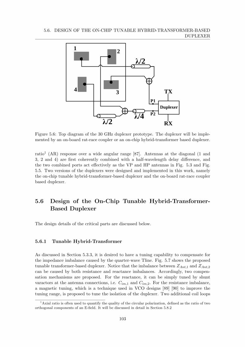
5.6. DESIGN OF THE ON-CHIP TUNABLE HYBRID-TRANSFORMER-BASEDDUPLEXER
λ/2
λ/2λ/4
Duplexer
RX
TX
1 2
34
P1
P2
Figure 5.6: Top diagram of the 30 GHz duplexer prototype. The duplexer will be imple-mented by an on-board rat-race coupler or an on-chip hybrid-transformer based duplexer.
ratio1 (AR) response over a wide angular range [87]. Antennas at the diagonal (1 and3, 2 and 4) are first coherently combined with a half-wavelength delay difference, andthe two combined ports act effectively as the VP and HP antennas in Fig. 5.3 and Fig.5.5. Two versions of the duplexers were designed and implemented in this work, namelythe on-chip tunable hybrid-transformer-based duplexer and the on-board rat-race couplerbased duplexer.
5.6 Design of the On-Chip Tunable Hybrid-Transformer-Based Duplexer
The design details of the critical parts are discussed below.
5.6.1 Tunable Hybrid-Transformer
As discussed in Section 5.3.3, it is desired to have a tuning capability to compensate forthe impedance imbalance caused by the quarter-wave Tline. Fig. 5.7 shows the proposedtunable transformer-based duplexer. Notice that the imbalance between ZAnt,1 and ZAnt,2can be caused by both resistance and reactance imbalances. Accordingly, two compen-sation mechanisms are proposed. For the reactance, it can be simply tuned by shuntvaractors at the antenna connections, i.e. Cim,1 and Cim,2. For the resistance imbalance,a magnetic tuning, which is a technique used in VCO designs [89] [90] to improve thetuning range, is proposed to tune the isolation of the duplexer. Two additional coil loops
1Axial ratio is often used to quantify the quality of the circular polarization, defined as the ratio of twoorthogonal components of an E-field. It will be discussed in detail in Section 5.8.2
103

CHAPTER 5. HYBRID-TRANSFORMER BASED DUPLEXER
ZAnt1
On-chipLNA
-90°°°°
Cre,1 Cre,2
Cim,1 Cim,2
TX+ -
ZAnt2
Figure 5.7: Proposed tunable transformer-based duplexer.
(a) (b)
Figure 5.8: (a) Schematic model of the transformer-based duplexer with magnetic tuning;(b) Simplified half schematic for analysis.
closed by varactors are placed at the two sides of the transformer. Intuitively it can beunderstood that when the real part of ZAnt1 is larger than that of ZAnt2, the coupledcurrent from the TX coil to the left side of the primary coil is lower than the coupledcurrent on the right side. By tuning Cre,2 to a larger value, the right side of the TX coilbecomes more coupled to the auxiliary coil with Cre,2, and less current is induced on theprimary coil on the right. This can compensate the reduced current on the left due to thehigher ReZAnt1, and no redundant TX current flows into the RX.
The principle of the magnetic tuning can be analyzed using the schematic shown inFig. 5.8(a). We assume here a symmetric transformer. In TX mode, there is a currenti1 flowing through L1,1 and L1,2. In case of imbalance, i.e. ZAnt,1 6= ZAnt,2, and without
104

5.6. DESIGN OF THE HYBRID-TRANSFORMER-BASED DUPLEXER
any tuning, the coupled current i2,1 is unequal to i2,2. The difference current flows intoRX, so TX/RX isolation is degraded. By tuning the capacitances (C3,1 and C3,2) in theauxiliary coils, i2,1 and i2,2 can be varied separately until they are equal. This can achieveisolation in case of imbalanced antenna impedances. When i2,1 = i2,2, the RX can be seenas a virtual ground for the differential TX signal, so we can simplify the schematic intohalf for the analysis, as shown in Fig. 5.8(b). In this case we obtain:
v2 = jωL2 · i2 + jωM1,2 · i1 + jωM2,3 · i3 (5.5)
v3 = jωL3 · i3 + jωM2,3 · i2 + jωM1,3 · i1 (5.6)
v2 = −i2 · ZAnt (5.7)
v3 = −i3 ·1
jωC3(5.8)
where M1,2,M2,3,M1,3 are the mutual inductances between the inductors shown in Fig.5.8. We assume that the coils have the same self inductance L, with a coupling coefficientof 1, i.e. L1 = L2 = L3 = M1,2 = M2,3 = M1,3 = L. Then we can derive that:
i2 = i1 ·jωL
jωL− (1− ω2LC3) · ZAnt(5.9)
We observe that if ZAnt is a real value and is changed, it can be compensated byvarying the value of C3. Referring back to Fig. 5.8(a), the following equation should besatisfied in order to have i2,1 = i2,2:
(1− ω2LC3,1) ·ReZAnt,1 = (1− ω2LC3,2) ·ReZAnt,2 (5.10)
This is the criteria for C3,1 and C3,2 to ideally compensate the real part imbalance of theantenna impedances. In practice, the coupling factor of the transformer is about 0.8 basedon the EM simulations. Comparing to the ideal case, for practical mutual inductances,larger tuning range on the Cre,1 and Cre,1 in Fig. 5.7 will be needed to compensate forthe same real part imbalance.
It is also interesting to note that in case of impedance variations, the proposed tuningmethod not only compensated the impedance imbalance to improve isolation, but alsocan partly improve impedance matching. For example, if ZAnt1 has a more capacitive orinductive imaginary part comparing to ZAnt2, by reducing or increasing the capacitancefrom the shunt varactor, not only the isolation can be improved, but it also compensatesthe matching on the imaginary part.
The simplified layout of the tunable duplexer is shown in Fig. 5.9. The primary coil inthe middle has the center tap connected to a co-planar waveguide (CPW) Tline with theground line connected through the transformer in the middle. The CPW further connectsto the LNA. The outer coil is the secondary coil connected to the TX. The coils, stackedby the top two metal layers, are 7 µm wide with 3 µm spacing. The varactors connectedto the inner auxiliary coils and the shunt varactors at the input of the primary coil canbe tuned to maximize the duplexer’s isolation.
The varactors used in the prototype design are reverse-biased junction diodes. Thecontrol voltages are DC coupled through large resistors, as shown in Fig. 5.9. The varac-tors in the auxiliary coils are in a differential configuration. The varactors can withstand
105

CHAPTER 5. HYBRID-TRANSFORMER BASED DUPLEXER
10
3 µ
m
Figure 5.9: Simplified layout of the tunable transformer-based duplexer.
a breakdown voltage of about 6 V. This corresponds to a maximum output power of 19.5dBm with a 50 Ohm antenna impedance at P1 and P2 in Fig. 5.6, and the simulated out-put 1-dB compression point is higher than this, as shown in Fig. 5.10. Besides the outputpower, linearity of the isolation is also important. As shown in the simulation result inFig. 5.10, below the breakdown level of the varactor, there is only minor degradation.In practice, to further increase the maximum output power and the isolation linearity,a multi-stacked technique [91] can be used to reduce the voltage swing across a singlevaractor.
5.6.2 Low Noise Amplifier
After the duplexer, a low-noise-amplifier (LNA) is also implemented. Fig. 5.11 shows theschematic of the single-ended two-stage LNA . The LNA has a cascode stage as the inputstage, which is optimized for simultaneous noise and gain matching [92]. The integratedduplexer makes it possible to optimize the impedance matching between the duplexerand the LNA, instead of a 50 Ω matching. The required optimum source impedance isobtained by optimizing the transformer dimension, and no extra input matching networkis necessary. The second stage is a common-emitter stage with higher voltage headroom
106

5.6. DESIGN OF THE HYBRID-TRANSFORMER-BASED DUPLEXER
−10 0 10 20 30
−10
0
10
20
30
PTX
(dBm)
Po
ut (
dB
m)
−10 0 10 20 30−60
−55
−50
−45
−40
−35
−30
Iso
lati
on
(d
B)
−10 0 10 20 30−60
−55
−50
−45
Figure 5.10: Simulated linearity of the duplexer, including output power (at either antennaports, Pout) and the isolation (between the RX and TX ports of the duplexer) versus theinput power at the TX port of the duplexer (PTX). The dashed parts are when PTX ishigher than 20 dBm, which might cause breakdown on the varactors and the simulationmodel might be not valid.
Figure 5.11: Schematic of the LNA.
to improve the output 1-dB compression point.
5.6.3 The Implemented IC
The on-chip hybrid-transformer-based duplexer and the LNA described above are designedin a 0.25 µm SiGe:C BiCMOS technology [93]. The die photo of the test chip is shownin Fig. 5.12, which consists of the transformer duplexer, LNA, and a balun for single-ended TX port measurement. The total chip area is 1.2 mm×0.8 mm, while the duplexer
107

CHAPTER 5. HYBRID-TRANSFORMER BASED DUPLEXER
0.8 mm
Figure 5.12: Chip micrograph.
occupies only about 0.25 mm×0.25 mm.
5.7 Design of the Demonstrator with On-Board Antennas
5.7.1 Sequentially-Rotated Circularly-Polarized Patch Antenna
An aperture-coupled microstrip antenna (ACMA) [64, 94, 95, 96] is used as a basic an-tenna element in the 2 × 2 array with sequential rotation. The substrate stack-up withhigh frequency Rogers materials is shown in Fig. 5.13. The patch antennas are printed onthe top metal layer, surrounded by a ground plane to reduce unwanted surface-wave prop-agation. The patch antennas are coupled through a slotted ground plane in the middlelayer, to the feed lines on the back side of the board. The top and middle ground layersare connected by abundant vias around the antennas. Compared to a patch antenna withdirect feed, the ACMA element can achieve a wider bandwidth [94].
The dimensions of the antenna structure and feed network are described in Fig. 5.14.The distance between the adjacent patch antennas is 7.5 mm, corresponding to 0.75λ ataround 30 GHz, in order to obtain a compromise between antenna size, mutual couplingand pattern characteristic [97]. Impedance matching is achieved mainly on the feed layer,using a stub of 0.65 mm long (effectively as a shunt capacitance) in combination with aninductive line in series. The input matching fractional bandwidth (S11 < −10 dB) atpoint P1 and P2 in Fig. 5.14 is more than 13% around 30 GHz in simulation. In the feedlayer, the 50 Ω microstrip Tline has a width of 0.45 mm in this stack-up. The lengths ofthe feed lines satisfy the length difference shown in Fig. 5.6. For simplicity, a non-isolatedreactive power combiner is used in this design. It consists of two 50
√2 Ω lines with length
108

5.7. DESIGN OF THE DEMONSTRATOR WITH ON-BOARD ANTENNAS
Patch18µm
Ground18µm
Feed18µm
RO43500.762mm
RO44500.1mm
RO43500.1mm
Figure 5.13: Stack-up of the antenna board.
of λ/4. If it is applied in a larger antenna array system and mutual coupling betweenantennas become more significant, an isolated wilkinson combiner can be used instead.
The dimensions of the final board design are optimized around 31 GHz 2. The length ofthe ground slot is optimized to obtain a double tuning [94], which improves the bandwidth.And more importantly, the impedances at P1 and P2 in Fig. 5.14 are optimized to be closeto each other around 31 GHz, which is important to achieve high isolation as explained inSection 5.3.3. The simulated impedances at P1 and P2 are shown in Fig. 5.15.
5.7.2 Wire-Bond Interface
The wire-bond interface between the chip and the antenna board shown in Fig. 5.16 iscritical to maintain the impedance matching for the desired bandwidth. For the wire-bonding, a cavity is made in the board with a depth of about 0.2 mm (in the used stack,the bottom of the cavity is the ground plane of the board), and the silicon die is placed init. The die has a substrate thickness of 0.22 mm. In this way, the required length of thewirebonds is minimized. Meanwhile, for the critical RF connections, the distance betweenthe cavity and the die edges uses the minimum allowable distance in order to minimize thelength of the wires for the critical 30 GHz signals. However, the bond wire with a diameterof 25 µm still has more than 300 pH inductance in our case. The impedance matching tocompensate the wire inductance on the RX port is explained in Fig. 5.16(b). The matchingconsists of a low impedance line (≈ 38 Ohm) and a high impedance line (≈ 80 Ohm) thatmatch the impedance before the bond wire to Z2, which is further matched to around 50
2As will be shown in the measurement results on the duplexer chip, the peak gain is shifted to 31 GHz.The antenna board design is thereafter fine-tuned and optimized accordingly.
109

CHAPTER 5. HYBRID-TRANSFORMER BASED DUPLEXER
Patch antenna
Patch groundGround slot
Feed
To duplexer
Reactive power combiner
1.78mm
1.80
mm
0.45mm1.82mm
0.18
mm
7.50
mm
4.68mm
P1P2
Figure 5.14: The dimensions of the aperture coupled microstrip antenna and the feed lines.
110

5.8. MEASUREMENT RESULTS
P1
P2
Figure 5.15: The simulated impedances at P1 and P2 seen from the duplexer are optimizedso that they are close to each other around 31 GHz.
Ohm after the bond wire. Notice that the ground-signal-ground bond wires connects to aco-planar waveguide transmission line which is part of the impedance matching. A similarmatching method is used for the antenna ports and the TX port.
The photographs of the manufactured and assembled prototypes are shown in Fig.5.17. The 2× 2 ACMA antenna array has a size of 19 ×19 mm2.
5.8 Measurement Results
In this section, measurement results will be presented, including the chip measurementand the final demonstrator with on-board antennas.
5.8.1 On-Chip Duplexer Measurement Results
To characterize the performance of the duplexer chip in Fig. 5.12, a full four-port on-wafer measurement was done, and the port assignment is annotated in Fig. 5.12. Fig.5.18 shows the simulated and measured input reflections and gain/loss for and the NF forthe RX/TX modes. For the RX mode, as shown in Fig.5.18(a), a measured gain of 18.0dB at 31 GHz is achieved when port 1 and 2 are excited with common-mode signals witha 3-dB bandwidth from 27.5 GHz to 34.5 GHz. The measured peak gain shifts slightly tohigher frequency and degrades by less than 1 dB. Notice that the simulated gain of thestandalone LNA without the duplexer at the input is 20.2 dB, which implies about 2.2dB insertion loss from the duplexer for the RX mode. The measured NF is about 4.0 dB,and the simulated NF is 3.3 dB. For the TX mode, as shown in Fig. 5.18, the measuredinsertion loss is 3.1 dB at 31 GHz when driving port 1 and 2 in differential mode. The 0.9
111

CHAPTER 5. HYBRID-TRANSFORMER BASED DUPLEXER
(a)
(b)
Figure 5.16: The interface between the microstrip lines and the chip using (a) wire-bondinterface; (b) the matching network breakdown.
112

5.8. MEASUREMENT RESULTS
Front Back
RX
TX37 mm
37 mm
19 mm
19 mm
x
y
φ
(a)
Front Back
Wire-bondedchip
RX TX
DC supplies and control
37 mm
19 mm
19 mm
57 mm
x
y
φ
(b)
Figure 5.17: Photograph of the demonstration boards with 2×2 linearly-polarized ACMAwith sequential rotation: (a) Using a rat-race coupler as duplexer; (b) Using the wire-bonded hybrid-transformer based duplexer chip covered with glob-top.
113
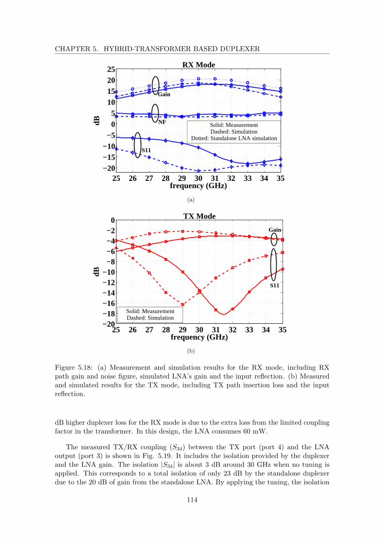
CHAPTER 5. HYBRID-TRANSFORMER BASED DUPLEXER
25 26 27 28 29 30 31 32 33 34 35−20−15−10−5
05
10152025
frequency (GHz)
dB
RX Mode
NF
S11
Gain
Solid: MeasurementDashed: Simulation
Dotted: Standalone LNA simulation
(a)
25 26 27 28 29 30 31 32 33 34 35−20−18−16−14−12−10−8−6−4−2
0
frequency (GHz)
dB
TX Mode
Gain
S11
Solid: MeasurementDashed: Simulation
(b)
Figure 5.18: (a) Measurement and simulation results for the RX mode, including RXpath gain and noise figure, simulated LNA’s gain and the input reflection. (b) Measuredand simulated results for the TX mode, including TX path insertion loss and the inputreflection.
dB higher duplexer loss for the RX mode is due to the extra loss from the limited couplingfactor in the transformer. In this design, the LNA consumes 60 mW.
The measured TX/RX coupling (S34) between the TX port (port 4) and the LNAoutput (port 3) is shown in Fig. 5.19. It includes the isolation provided by the duplexerand the LNA gain. The isolation |S34| is about 3 dB around 30 GHz when no tuning isapplied. This corresponds to a total isolation of only 23 dB by the standalone duplexerdue to the 20 dB of gain from the standalone LNA. By applying the tuning, the isolation
114

5.8. MEASUREMENT RESULTS
25 26 27 28 29 30 31 32 33 34 35
−50
−40
−30
−20
−10
0
frequency (GHz)
S34
(dB
)S34 without tuning
ISOLDUP
= 40 dB
S34 tuned around different frequencies
Figure 5.19: Measured port isolation (S34) of the duplexer chip, including the 20 dB gainfrom the standalone LNA. The isolation of the duplexer standalone (ISOLDUP ) around30 GHz is calculated by subtracting the LNA’s gain from the S34.
can be significantly improved. |S34| can be tuned to be higher than 20 dB for a bandwidthof 2 GHz around 31 GHz, as shown in Fig. 5.19, and it corresponds to a duplexer isolationof more than 40 dB. The bandwidth of a 45 dB duplexer isolation is about 1 GHz. Theaggregated bandwidth of the high isolation by the on-chip tunable duplexer is more than7 GHz, from 27 to 34 GHz.
Figure. 5.20 shows the tuning range of the on-chip tunable duplexer. The measurementis done using a source-pull at Ant1 port (port 1 in Fig. 5.12) and calibrated 3-portmeasurements are done on the other three ports for different source impedances at theAnt1 port. The calibrated 3-port measurement can measure the isolation between RX andTX port when the Ant2 port is terminated by 50 Ω. The discrete points are the measuredsource impedances at Ant1 that can be tuned for more than 50 dB isolation at 31 GHz bythe on-chip duplexer. The interpolated impedances within the range are tunable for highisolation. This range is sufficient for typical radar applications. For cellular applicationswhere the antenna impedance can vary significantly, the tuning range can be extended byincreasing the capacitance tuning ratio of the varactors, and even antenna tuning unitsmight be necessary to confine the antenna impedance [24]. Note that the tuning rangein Fig. 5.20 is shifted towards the capacitive part of the Smith chart. This is due to theimbalance in the complete layout of the on-chip hybrid-transformer. It is also the mainreason for the low isolation before tuning in Fig. 5.19. Thanks to the on-chip tunability,the impact can be compensated and high isolation can be achieved.
A performance summary of the duplexer chip and a comparison to other state-of-artstandalone duplexers [76, 77, 78, 24, 80, 98] are listed in Table. 5.1. The duplexersworking at around 2 GHz [24, 80, 98] which use the similar technique achieve the similarlevel isolation, but their loss is higher. This is because of the inherent power loss due to the
115
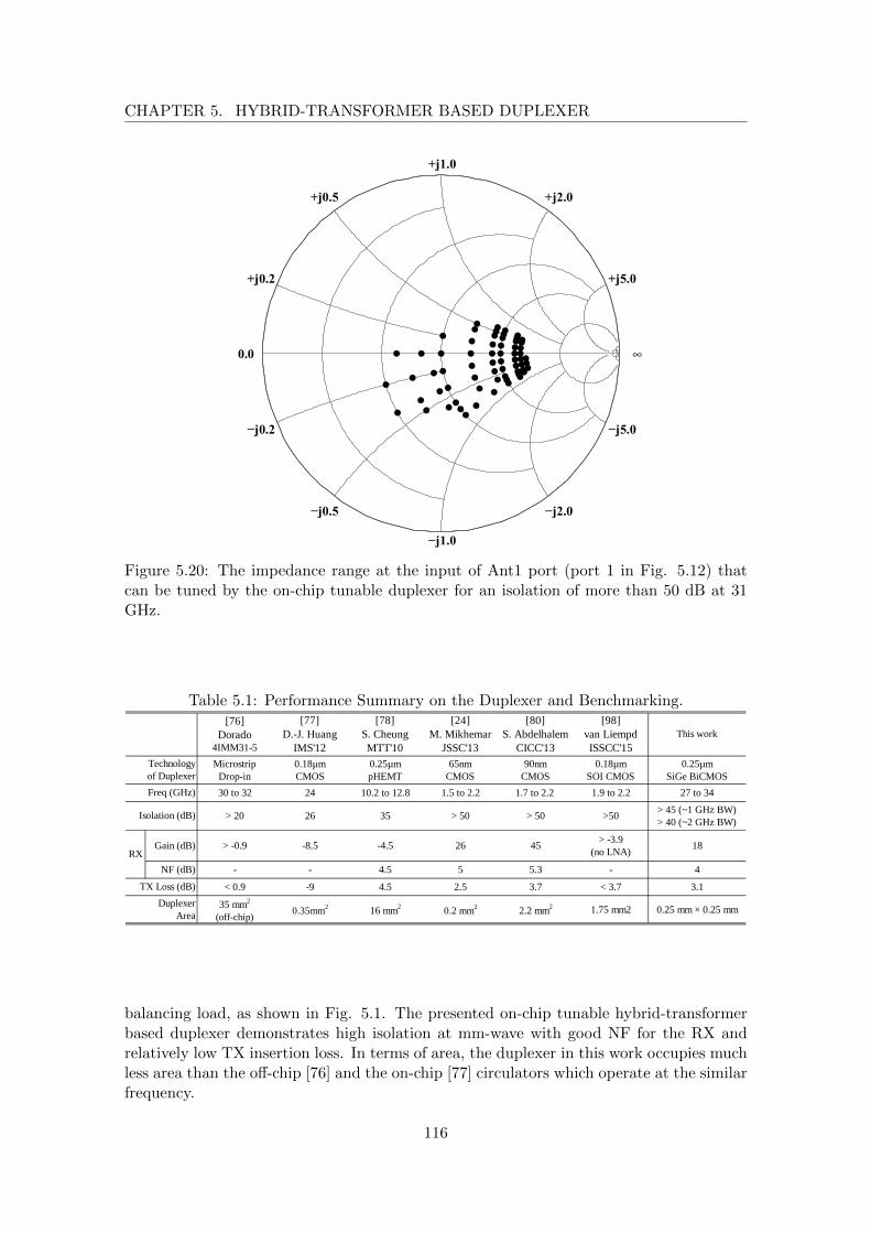
CHAPTER 5. HYBRID-TRANSFORMER BASED DUPLEXER
+j0.2
−j0.2
+j0.5
−j0.5
+j1.0
−j1.0
+j2.0
−j2.0
+j5.0
−j5.0
0.0
Figure 5.20: The impedance range at the input of Ant1 port (port 1 in Fig. 5.12) thatcan be tuned by the on-chip tunable duplexer for an isolation of more than 50 dB at 31GHz.
Table 5.1: Performance Summary on the Duplexer and Benchmarking.
MicrostripDrop-in
0.18µmCMOS
0.25µmpHEMT
65nmCMOS
90nmCMOS
0.18µmSOI CMOS
0.25µmSiGe BiCMOS
30 to 32 24 10.2 to 12.8 1.5 to 2.2 1.7 to 2.2 1.9 to 2.2 27 to 34
> 20 26 35 > 50 > 50 >50> 45 (~1 GHz BW)> 40 (~2 GHz BW)
Gain (dB) > -0.9 -8.5 -4.5 26 45> -3.9
(no LNA)18
NF (dB) - - 4.5 5 5.3 - 4
< 0.9 -9 4.5 2.5 3.7 < 3.7 3.1
35 mm2
(off-chip)0.35mm2 16 mm2 0.2 mm2 2.2 mm2 1.75 mm2 0.25 mm × 0.25 mm
TX Loss (dB)
Duplexer Area
This work
Technology of Duplexer
Freq (GHz)
Isolation (dB)
RX
[80]S. Abdelhalem
CICC'13
[76]Dorado
4IMM31-5
[77]D.-J. Huang
IMS'12
[78]S. CheungMTT'10
[24]M. Mikhemar
JSSC'13
[98]van LiempdISSCC'15
balancing load, as shown in Fig. 5.1. The presented on-chip tunable hybrid-transformerbased duplexer demonstrates high isolation at mm-wave with good NF for the RX andrelatively low TX insertion loss. In terms of area, the duplexer in this work occupies muchless area than the off-chip [76] and the on-chip [77] circulators which operate at the similarfrequency.
116

5.8. MEASUREMENT RESULTS
25 26 27 28 29 30 31 32 33 34 35−40
−30
−20
−10
0Isolation (Rat−race)
frequency (GHz)
dB
Figure 5.21: Measured isolation of the antennas with rat-race coupler as duplexer.
5.8.2 Demonstrator Measurement Results
The measurement of the demonstration boards in Fig. 5.17 consists of two parts. First, wemeasured the isolation between the RX and TX ports on both the rat-race coupler versionand the on-chip duplexer version. Next to the isolation, the impact on the antenna patternsand the purity of the circular polarization (CP) are also crucial, especially after tuningfor high isolation for the on-chip duplexer case. So secondly, we measured the antennapatterns and the corresponding axial ratio. The CP antenna patterns in the principleplane (φ = 0) are characterized using an LP reference antenna which measures the x-and y-component of the total electric field, i.e. Ex and Ey. The used coordinate definitionis shown in Fig. 5.17. The RHCP and LHCP patterns in the principle plane are:
ERHCP =
√2
2· (Ex + Ey · j) (5.11)
ELHCP =
√2
2· (Ex − Ey · j) (5.12)
and the axial ratio (in dB) is:
AR = 20log10
(∣∣∣∣ |ERHCP |+ |ELHCP ||ERHCP | − |ELHCP |
∣∣∣∣) (5.13)
Results of the Rat-Race Coupler
The measured isolation between the RX and TX ports in the prototype using a rat-racecoupler is shown in Fig. 5.21. It can achieve an RX/TX isolation of around 20 dB around31 GHz. For the antenna performance, both the RX and TX mode have an antenna gainof about 6.5 dBi at 31 GHz at broadside, and the 3 dB beamwidth is about 34, as shownin Fig. 5.22. The desired patterns of the RX and TX mode are in orthogonal polarizations,i.e. the co-polarizations of RX and TX mode are in LHCP and RHCP respectively. Thecross-polarizations of both modes are more than 18 dB as compared to the co-polarizationcomponent at broadside. This corresponds to an AR of lower than 2 dB, as shown in Fig.5.23.
117
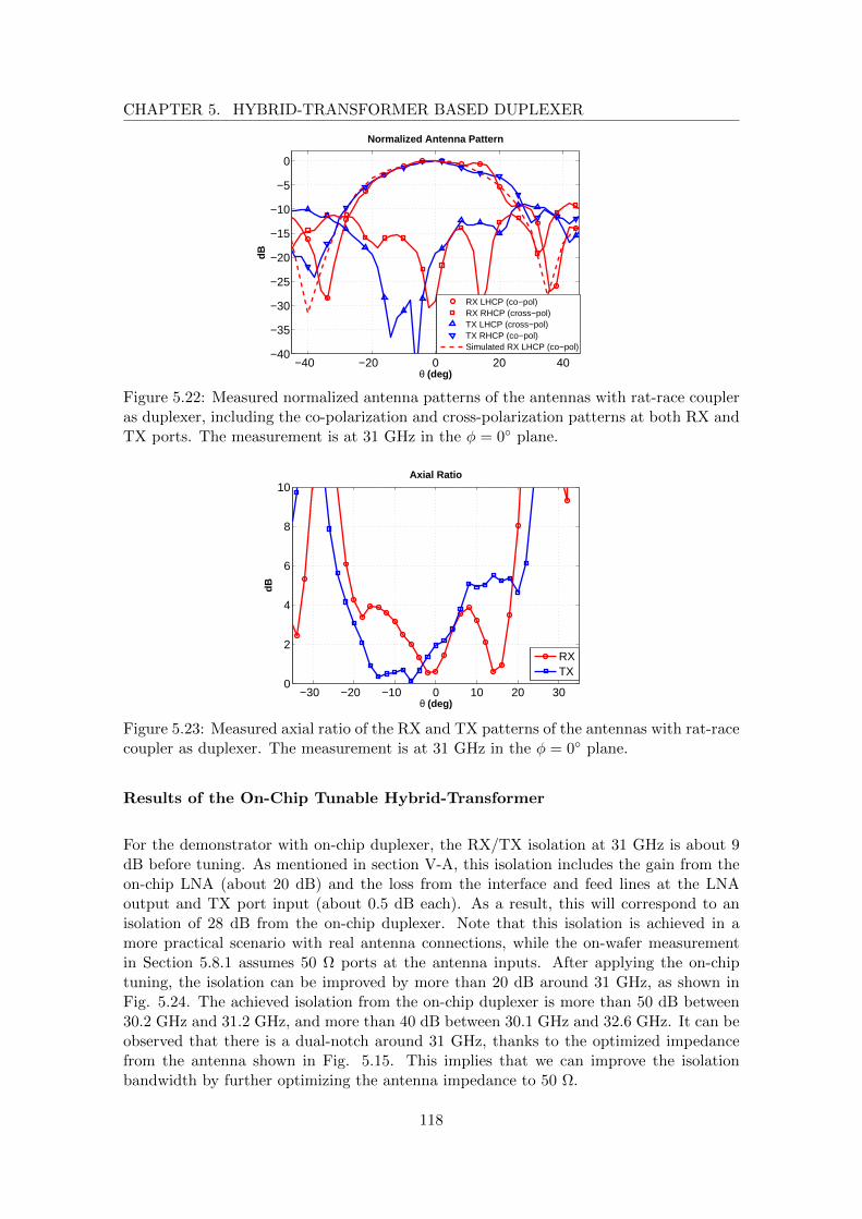
CHAPTER 5. HYBRID-TRANSFORMER BASED DUPLEXER
−40 −20 0 20 40−40
−35
−30
−25
−20
−15
−10
−5
0
Normalized Antenna Pattern
θ (deg)
dB
RX LHCP (co−pol)RX RHCP (cross−pol)TX LHCP (cross−pol)TX RHCP (co−pol)Simulated RX LHCP (co−pol)
Figure 5.22: Measured normalized antenna patterns of the antennas with rat-race coupleras duplexer, including the co-polarization and cross-polarization patterns at both RX andTX ports. The measurement is at 31 GHz in the φ = 0 plane.
−30 −20 −10 0 10 20 300
2
4
6
8
10Axial Ratio
θ (deg)
dB
RXTX
Figure 5.23: Measured axial ratio of the RX and TX patterns of the antennas with rat-racecoupler as duplexer. The measurement is at 31 GHz in the φ = 0 plane.
Results of the On-Chip Tunable Hybrid-Transformer
For the demonstrator with on-chip duplexer, the RX/TX isolation at 31 GHz is about 9dB before tuning. As mentioned in section V-A, this isolation includes the gain from theon-chip LNA (about 20 dB) and the loss from the interface and feed lines at the LNAoutput and TX port input (about 0.5 dB each). As a result, this will correspond to anisolation of 28 dB from the on-chip duplexer. Note that this isolation is achieved in amore practical scenario with real antenna connections, while the on-wafer measurementin Section 5.8.1 assumes 50 Ω ports at the antenna inputs. After applying the on-chiptuning, the isolation can be improved by more than 20 dB around 31 GHz, as shown inFig. 5.24. The achieved isolation from the on-chip duplexer is more than 50 dB between30.2 GHz and 31.2 GHz, and more than 40 dB between 30.1 GHz and 32.6 GHz. It can beobserved that there is a dual-notch around 31 GHz, thanks to the optimized impedancefrom the antenna shown in Fig. 5.15. This implies that we can improve the isolationbandwidth by further optimizing the antenna impedance to 50 Ω.
118

5.8. MEASUREMENT RESULTS
25 26 27 28 29 30 31 32 33 34 35−40
−30
−20
−10
0
Isolation (Chip)
frequency (GHz)
dB
InitialAfter tuning
ISOLDUP
= 40 dB
ISOLDUP
= 50 dB
Figure 5.24: Measured RX/TX port isolation of the antennas with on-chip hybrid-transformer based duplexer, before and after tuning for high isolation. It includes gainfrom the LNA.
The antenna pattern for the prototype with on-chip duplexer shows a similar 3 dBbeamwidth for both RX and TX patterns, before and after tuning, as shown in Fig. 5.25.The co-polarizations of the RX and TX are in orthogonal circular polarizations. Thecross-polarization by the TX is more than 19 dB below the co-polarization, and an axialratio (AR) of below 2 dB is achieved as demonstrated in Fig. 5.26. The TX AR is lessinfluenced after the tuning than the RX. For the RX, the AR is about 3.8 dB at broadside,which is degraded by about 1.2 dB after the tuning is applied.
The impact of the relatively high RX AR can be two-fold in practice. First, it canincrease polarization loss. In case of receiving a pure LHCP signal, an RX AR of 5 dBleads to a polarization loss of less than 0.35 dB, which is acceptable for most applications.Second, it has only a rejection ratio of about -11 dB to an interference signal with RHCP.This RHCP interference can be from its own TX, e.g. the LHCP signal from the TXmode (-19 dB lower than the RHCP signal as shown in Fig. 5.25) will be RHCP afterreflection for the RX. Including the path loss in air (e.g. 42 dB for 0.1 m at 31 GHz), thereceived RHCP signal from the reflected TX signal can be attenuated by more than 78dB in total, which is not going to degrade the duplexer isolation. However, if the receivedRHCP signal is from other systems, this might give interference problems. The degradedRX AR in Fig. 5.26 is probably due to undesired coupling between the wire-bonds in thiswork. The reason that the RX is more influenced is because there is also LNA on-chip,which amplifies the undesired coupled signals. The AR can be improved by increasing thedistance between the high frequency wire-bonds and/or by using more advanced packagingtechnologies, e.g. flip-chip interconnects.
119

CHAPTER 5. HYBRID-TRANSFORMER BASED DUPLEXER
−40 −30 −20 −10 0 10 20 30 40−30
−25
−20
−15
−10
−5
0
Normalized Antenna Pattern
θ (deg)
dB
RX LHCP (co−pol)RX RHCP (cross−pol)TX LHCP (cross−pol)TX RHCP (co−pol)
Figure 5.25: Measured normalized antenna patterns of the antennas with on-chip hybrid-transformer based duplexer, including the co-polarization and cross-polarization patternsat both RX and TX ports, before and after tuning for high isolation. The initial patternsare shown as solid lines, while the patterns after tuning for high isolation are denoted asdashed lines. The measurement is at 31 GHz in the φ = 0 plane.
−30 −20 −10 0 10 20 300
2
4
6
8
10Axial Ratio
θ (deg)
dB
RX initialTX initialRX optimized for isolationTX optimized for isolation
Figure 5.26: Measured axial ratio of the RX and TX patterns of the antennas with on-chip hybrid-transformer based duplexer, before and after tuning for high isolation. Themeasurement is at 31 GHz in the φ = 0 plane.
5.9 Discussions on Potential Extensions
Other than the particular implementation in this chapter, the duplexer concept in Fig.5.2 and Fig. 5.3 can be varied and extended for different applications, a few of which arediscussed below:
• The on-board quarter-wave Tline can be replaced by lumped on-chip componentsfor higher integration, especially for applications at higher frequencies with on-chip
120

5.10. SUMMARY AND CONCLUSIONS
antennas [99]. This can be done by using a high-pass LC filter with +45 phaseshift and a low-pass LC filter with −45 phase shift on the two sides of the primarycoil of the hybrid-transformer. In this way, a wide-band 90 phase difference can beachieved, with a more balanced ohmic loss on the two sides. Notice, however, thatthe impedance transformation still exists in this case just as in the configuration inFig. 5.3(a).
• A rat-race coupler potentially can replace the hybrid-transformer, as in Fig. 5.5, andcan be extended to on-chip implementation at higher frequencies. Furthermore, therat-race coupler can be extended with tuning capabilities, in order to achieve highisolation in practice. One possible implementation of the tunability is the distributedtunable Tline [50].
• For applications which are area-limited, a dual-feed single-patch antenna [100] is analternative for the sequentially rotated 2 × 2 array. The configuration in Fig. 5.2with a dual-feed single-patch antenna can be very compact and might be interestingfor lower frequency applications, e.g. WLAN and cellular.
• It is valuable to have tunable dual notches by the tunable duplexer for FDD com-munication applications [80, 81]. This is necessary for such applications not only toisolate the large blocker at the TX band, but also to isolate the noise generated by theTX around the RX band. This might be achieved by extra degrees-of-freedom andcomplexity in the tuning circuitry which however will inevitably increase insertionloss.
• A tunable duplexer with a larger bandwidth is another interesting topic in orderto make better use of the available wide bandwidth at mm-wave frequencies. Themost obvious solution to this on the proposed configuration is a wide-band antennadesign with an input impedance sufficiently close to 50 Ω, so that the impedancetransformation by the quarter-wave Tline is minimized. A tunable duplexer withdual or even multiple notches is also a potential solution to increase the isolationbandwidth.
5.10 Summary and Conclusions
This chapter has presented a novel mm-wave circular polarization duplexer concept withon-chip hybrid-transformer. The proposed technique duplexes the orthogonal linearly-polarized antennas by the circularly-polarized TX and RX signals with high TR/RX iso-lation. An on-chip tuning mechanism is further proposed for optimizing the isolation incase of impedance imbalance. The on-chip duplexer demonstrates high isolation with lowNF for the RX path and low insertion loss for the TX path. Two antenna prototypesintegrated with the on-chip duplexer and with an on-board rat-race coupler have been de-signed and implemented. Orthogonal circular polarizations are demonstrated for the TXand RX. The on-chip tunable duplexer prototype achieves a high isolation of more than50 dB around 31 GHz. The proposed circular polarization duplexer concept is especiallysuitable for radar and imaging applications, offering the possibility of full integration incombination with low loss and high isolation.
121

CHAPTER 5. HYBRID-TRANSFORMER BASED DUPLEXER
122

Chapter 6
Conclusions andRecommendations
6.1 Conclusions
This thesis focuses on interference scenarios for future millimeter-wave wave (mm-wave)applications. Two interference issues are investigated, i.e. spatial interference and selfinterference.
The first investigated issue is spatial interference suppression. In order to compensatethe high path loss at mm-wave frequencies and maintain the required link budget, phasedarrays are typically used. Thanks to the directivity of a phased array system, certainspatial re-use can be obtained. However, the spatial re-use is not fully explored in today’smm-wave phased arrays. It is demonstrated in this thesis that the interferences enteringthe side-lobes can degrade the signal-to-interference ratio (SINR). Null-forming is a knowntechnique for spatial interference mitigation, especially when the spectrum gets crowdedin future applications. However, practical impairments in the analog/RF phase shift andamplitude weights and the pre-knowledge of the interference direction hampers the accu-rate control over the spatial nulls. With some reasonable impairments, the resulted SINRby a conventional null-forming array can even degrade to the case with no optimizationat all.
To achieve a robust null-forming, an adaptive array assisted with an efficient geneticalgorithm (GA) optimization is proposed in this work, which can efficiently find the properweights to decrease the received undesired power, thereby improving the SINR. It is shownthat nulls can be formed with a small number of iterations with significant improvementon the SINR and spatial re-use gain. It is also shown that the method is robust to weighterrors. It can be a useful method for practical analog/RF phased arrays at mm-waverange to exploit the spatial re-use as an extra resource (on top of the frequency divisionand time division), which can help co-existence between different links and/or increase thetotal network throughput efficiently.
The proposed adaptive analog/RF null-forming array requires a high resolution phase
123

CHAPTER 6. CONCLUSIONS AND RECOMMENDATIONS
shifter (6-bit or comparable I/Q modulated constellation points). This is necessary tohave a good main-lobe coverage for a uniform linear array (ULA) of 8 or 16 elements.Meanwhile, it provides extra degrees-of-freedom so that the null-forming array is able totune the array pattern to place nulls in certain directions. As an enabler for the proposednull-forming array, the required phase shifter for 60 GHz applications is investigated in thisthesis. In a sliding-IF receiver front-end architecture, two versions of suitable phase shiftersare implemented in a 40-nm CMOS technology, i.e. an LO-path phase shifter (LOPS) anda baseband phase shifter (BBPS). The LOPS achieves a resolution of 5.4, i.e. about 6-bit,from 44 GHz to 54 GHz, and the BBPS achieves in total 225 constellation points for bothphase and amplitude adjustment. Both designs are suitable for the proposed adaptivenull-forming array.
Another potential scenario in mm-wave front ends is self interference from the co-located transmitter. The high power self interference can cause saturation and desensi-tization of the receiver. The self interference scenario can further be divided into twosituations depending on the frequency separation between the transmitter and receiver.
First, the separation can be relatively high, e.g. in a very-small-aperture-terminal(VSAT) scenario when the transmitter and receiver are around 30 GHz and 20 GHzrespectively. The VSAT scenario requires a receiver with ultra low noise figure (NF) below2 dB. It is challenging to achieve the required high isolation with low loss and minimalimpact on the NF. A 20 GHz LNA design with integrated passive filtering is proposed toachieve this. It is found that an optimum trade-off between stop-band attenuation andtotal pass-band NF can be obtained by properly applying filtering at different stages ofthe LNA. Furthermore, co-designing the filter and matching can further reduce the addedimpact of passive filtering on the receiver. Implemented in a SiGe BiCMOS 0.25 µmtechnology, the filtering LNA achieves an attenuation of more than 30 dB from 27.5 GHzto 31 GHz with a 0.1 dB to 0.4 dB degradation on the NF, comparing to a reference LNAdesign without any filtering. This integrated solution can be used for future Ka-bandVSAT full-duplex applications. A similar approach can be used in the PA design to filterthe noise around 20 GHz.
The second scenario for self-interference is when the transmitter and receiver are closein frequency. In this case, passive filtering is not suitable due to the limited on-chip qualityfactor, and a duplexer is typically used. At mm-wave, however, the ferrite-based circula-tors and the on-chip active circulators have limited isolation. For this scenario, a mm-wavecircular polarization duplexer concept using an on-chip tunable hybrid-transformer is pre-sented. The proposed technique is based on the concepts of a hybrid-transformer andcircular polarization. It is capable of duplexing orthogonal linear-polarized antennas bythe circularly-polarized TX and RX signals with high TX/RX isolation. A 30 GHz du-plexer test-chip integrated with an LNA is implemented in a SiGe BiCMOS 0.25 µmtechnology. In order to demonstrate the polarizations and the isolation with antennaconnections, two antenna prototypes integrated with the on-chip duplexer and with anon-board rat-race coupler have been implemented. Orthogonal circular polarizations aredemonstrated for the TX and RX. The on-chip tunable duplexer prototype achieves a highisolation of more than 50 dB around 31 GHz. This proposed circular polarization duplexerconcept is especially suitable for radar and imaging applications, offering the possibility offull integration in combination with low loss and high isolation. It also has the potentialto extend to communication applications.
124
6.2. ORIGINAL CONTRIBUTIONS
In conclusion, methods and high performance circuits in silicon technologies are devel-oped in this thesis for the spatial and self interference issues in mm-wave integrated frontends. Practical challenges of null-forming in a mm-wave phased array are investigated anda robust method is proposed for better exploring the spatial interference mitigation. Asa critical block in the method, high resolution phase shifters are implemented in CMOStechnology. As the usage of wireless systems at mm-wave becomes more and more pop-ular in the future, we can envision that the proposed method can be useful in improvingthe co-existence and the total throughput. For the self interference issues between theco-located TX and RX, high performance fully integrated circuits are implemented inBiCMOS technology, i.e. a filtering LNA and a hybrid-transformer based duplexer. Themeasurement results show competitive performance to traditional off-chip components,e.g. waveguide-based or ferrite-based components. Due to the reduced form factor, lowersystem cost and lower interconnect complexity, the fully integrated techniques are veryattractive solutions for future mm-wave front ends.
6.2 Original Contributions
• Investigation of the practical impairments in a phased array and the impacts onnull-forming. Accordingly, a robust null-forming method is proposed for spatialinterference mitigation in mm-wave phased array receivers.
• Design and implementation of two high resolution phase shifters in a 60 GHz frontend, i.e. a LO-path phase shifter and a baseband phase shifter.
• Design and implementation of a filtering LNA for self interference suppression infull-duplex VSAT applications.
• Proposal for a circular polarization duplexer method.
• Design and implementation of an on-chip hybrid-transformer based duplexer.
• Design and implementation of a demonstration board with on-board antennas, anda wire bonding interface to the duplexer chip.
6.3 Recommendations for Future Work
• The null-forming receiver array as proposed in Chapter 2 minimizes spatial interfer-ence reception. A more global optimization is interesting to investigate. Nulls canalso be generated in the array pattern of a transmitter array. If the desired receiverarray pattern and interference transmitter array pattern can be jointly optimized,even more spatial re-use gain can be obtained. Co-ordination is necessary in thiscase between the desired receiver and the interfering transmitter(s).
• For the null-forming array, it is interesting to investigate different algorithms forthe optimization. The presented usage of a genetic algorithm demonstrates goodperformance in terms of SINR improvement and convergence. However a thoroughinvestigation on alternative algorithms can be interesting to further improve the
125

CHAPTER 6. CONCLUSIONS AND RECOMMENDATIONS
speed. Besides, a microprocessor implemented on-chip for the algorithm is also veryinteresting and valuable for full integration and for real-time applications.
• In practice, mutual coupling between antenna elements can also influence the totalarray pattern. Potentially, the genetic algorithm assisted array can also compensatethe effect of mutual coupling, and minimize the total received interference power.For practical use, it is interesting and useful to take the mutual coupling into accountin the proposed method.
• For the filtering LNA presented in Chapter 4, it is also important to investigate theimpact of the packaging and interface to the antenna on the total NF. One stepfurther, it is also interesting to take the packaging/interface into consideration at anearly stage, and to co-design it as part of the filter. For example, the bond-wire atthe RF input can be an inductor with very high quality factor.
• The passive filtering method can be extended to the power amplifier design at thetransmitter side. This can suppress the transmitter noise which can be coupled tothe receiver and raise the noise floor.
• For the circular polarization duplexer proposed in Chapter 5, the axial ratio of thereceiver’s polarization should be improved. It can be improved by a better design ofthe wire-bond interface to avoid undesired coupling, or by more advanced packagingtechnologies, e.g. flip-chip.
• The duplexer concept can be extended to higher frequencies (e.g. 100 GHz) and tofull integration with on-chip antennas.
• The tunable hybrid-transformer based duplexer with dual identical antennas canbe suitable for low frequency applications, e.g. multi-standard cellular applications.Single-patch dual-feed antennas can be used for a compact size. It is interesting toinvestigate its performance and feasibility.
• It is worthwhile to extend the hybrid-transformer based duplexer with dual notchesfor frequency-division-duplex based communication applications.
126

Appendix A.Phase Shift and Time Delay
In Chapter 3, we used a narrow-band phase shift (φk) approximation in the weight tuning.However, the received signal at each antenna actually have a time delay difference, andthe phase approximation is not enough to compensate the time delays for a wide-bandsignal, and using a phase shift will lead to a frequency-dependent beam-steering. In thisappendix, we examine the effect of the phase approximation, and validates our usage ofphase shifts in the 60 GHz single-channel communication application.
First, we revisit the array factor by using time delays. We can replace the phase shiftsφk in equation (2.4) in Chapter 3 by 2πf · τk for k = 1, · · · , N , as below:
AFτ (f, θ) =
N∑k=1
ak · e−j·2πf ·
((k−1)d·sin(θ)
c+τk
)(A.1)
For beam-steering towards direction θs, we can set ak = 1, and the time delay for eachpath for beam-steering as:
τk = −(k − 1)d · sin(θs)
c, for k = 1, · · · , N (A.2)
In this case, independent of the frequency, the array factor at direction θs is alwaysmaximum, i.e. AFτ (f, θs) , N .
If a phase shift approximation is made on the time delay at a center frequency of fc,then the corresponding phase shift of (A.2) is:
φk = −2πfc ·(k − 1)d · sin(θs)
c, for k = 1, · · · , N (A.3)
Using the phase shift in (A.3), the array factor then becomes:
AFφ(f, θ) =N∑k=1
ak · e−j2πd·(k−1)
c·[f ·sin(θ)−fc·sin(θs)] (A.4)
From (A.4), we can see the maximum array factor at f is steered towards a frequency-dependent direction:
θmax(f) = arcsin(f
fc· sin(θs)) (A.5)
127

APPENDIX . A. PHASE SHIFT AND TIME DELAY
−80 −60 −40 −20 0 20 40 60 80−20
−10
0
10
20
Using time delay
θ (in degrees)
dB
fcfc +
∆f2
fc −∆f2
(a)
−80 −60 −40 −20 0 20 40 60 80−20
−10
0
10
20
Using phase shift
θ (in degrees)
dB
fcfc +
∆f2
fc −∆f2
(b)
Figure A.1: The array patterns using (a). time delay and (b). phase shift. The antennasare assumed with d = λ
2 spacing, with N = 16 and FBW = 20%.
In other words, for the desired direction, the array will experience a different arrayfactor. This is illustrated in Fig. A.1, which is simulated on a 16-element array withd = λ/2 spacing and the array is beam-steered towards θs = 30. The figure showsarray factors at the center frequency and the lowest and highest frequencies using timedelay and phase shift respectively. The fractional bandwidth is assumed to be 20%, i.e.FBW = ∆f
fc= 20%. It can be observed that at θs, the main-lobe peaks of the array
factors using time delay are frequency independent, while the peaks using phase shift areshifted for the lowest and highest frequencies within the FBW . And the main-lobe gainsat θs are dropped for the two edge frequencies. This effect is also called beam squint [34].The effect of beam squint due to the phase shift approximation is dependent on the FBWof the signal, the size of the array and also the maximum AoA. Actually we can quantifythe beam squint effect by the gain loss of the array factor in a certain desired direction θsas follows.
Consider a wide-band signal with a fractional bandwidth of FBW = ∆ffc
, we can derivethe variation on the array factor towards the desired direction. The absolute value of thearray factor towards θs at the lowest and highest frequency, i.e. fc ± ∆f
2 , can be denoted
128

0 5 10 15 20 25 30 35 400
1
2
3
4
5
6∆SNRφ at θs = 30
Fractional Bandwidth (%)
dB
N = 4N = 8N = 16
(a)
0 5 10 15 20 25 30 35 400
5
10
15
20∆SNRφ at θs = 60
Fractional Bandwidth (%)
dB
N = 4N = 8N = 16
(b)
Figure A.2: The SNR loss due to beam squint using phase shift instead of time delay,versus the FBW for N = 4, 8, 16 when (a). θs = 30, and (b). θs = 60. The antennasare assumed with d = λ
2 spacing.
as: ∣∣∣∣AFφ(fc ±∆f
2, θs)
∣∣∣∣ =
∣∣∣∣∣N∑k=1
e−j2πd·(k−1)
c·[(fc±∆f
2)·sin(θs)−fc·sin(θs)]
∣∣∣∣∣=
N if θs = 0√
1−cos[N ·πdc ·∆f ·sin(θs)]1−cos[πdc ·∆f ·sin(θs)]
if θs 6= 0
(A.6)
With (A.6), we can get the SNR loss comparing to the maximum achievable SNR, i.e.N :
∆SNRφ(∆f,N, θs) = 10 log10
(1
N·∣∣∣∣AFφ(fc ±
∆f
2, θs)
∣∣∣∣) (in dB) (A.7)
From (A.6) and (A.7), we can decide how much the influence is on the main-lobe gaindue to the phase shift approximation for certain applications, based on the requirements
129
APPENDIX . A. PHASE SHIFT AND TIME DELAY
on signal bandwidth, number of antenna’s and the maximum steering direction. We canplot the corresponding ∆SNRφ for different values of FBW , N and θs, as shown in Fig.A.2. It can be observed that the SNR loss increases with larger N , larger FBW and/orlarger θs. It is also interesting to notice that in Fig. 2(b), significant loss happens for a16-element array when the FBW is 29%. This is because the shift of the main-lobe at theedge frequencies is so large that a null is placed towards θs.
For the 60 GHz application that we are looking at in Chapter 2, the recent standard[12] locates four channels, each with a bandwidth of 2.16 GHz, around the 60 GHz band.In this work, we consider scenarios with dense links in the environment, and most linksare using a single channel at the same time. For the usage of a single channel, the FBW is3.6%, which corresponds to a maximum SNR loss of only 0.11 dB for ±60 steering rangeby a ULA of size 16. As a result, in Chapter 2 and Chapter 3, phase shift will be usedfor weight control instead of time delay. Ultimately, in case of channel bonding on all thefour channels, the SNR loss is 1.9 dB for the same steering angle and array size, and itwill be more severe for even larger sizes of a linear array (although it is not common incommercial applications) which will tend to require time delays in the array system.
130

Appendix B.Genetic Algorithm for theNull-Forming Array
Instead of the closed-form max-SINR solution introduced in Chapter 2, the method pro-posed in the same chapter is to find the optimum weights by a genetic algorithm (GA)which minimizes the received noise plus interference power. Fig. 2.8 shows the receiverarchitecture for this GA assisted adaptive array. In each array path, the most-significant-bits (MSBs) of the phase-shifters are dedicated for controlling the mainlobe, while theleast-significant-bits (LSBs) are used to add perturbation to the array pattern to formnullings at certain directions. The main-lobe can be controlled or shifted by only usingthe phase-shifters, so the MSBs of the amplitude bits are always set to 1’s and thereforenot shown in Fig. 2.8. The LSB perturbations on the phase-shifters and VGAs will onlyslightly influence the mainlobe.
Algorithm Description
In this appendix, we will describe the GA in detail. There are two important conceptsin GAs, chromosome and population. A chromosome denotes a string of settings for thephase-shifters and the VGAs on each antenna’s path. In our case, since we use discretephase-shifters and VGAs, a chromosome is a concatenation of the LSBs of every antennapath’s phase and amplitude setting. All different chromosomes together form a populationof size Npop. The basic idea of a GA is to evolve the population by many iterations(generations) until a chromosome achieves the optimization goal. The optimization goalin our application is to minimize the total received interference power plus the noise floorbelow a minimum power threshold.
The algorithm procedure is shown in Fig. 2.9. The GA core starts by an initializationof the populations. In the initialization, half of the chromosomes are randomly generated,while the other half are the complement of the first half. This increases the diversity of thechromosomes (or the coverage on the search space) and may reduce the convergence time.Second step is to evaluate the chromosomes. Apply every chromosome’s setting to thephase shifters and VGAs, and the corresponding received interference plus noise power ismeasured, and they are sorted in an ascending order. If the minimum power threshold isreached by one or more chromosomes, the best chromosome is selected and the algorithmis finished. Otherwise, it continues to refresh the populations for the next iteration.
131

APPENDIX . B. GENETIC ALGORITHM FOR THE NULL-FORMING ARRAY
In the next step, the worse chromosomes (with a discard rate of RD = 50%) in thesorted population are discarded. The survived populations are then selected into pairs andthey create two off-springs by crossover. The selection method in this GA uses roulettewheel weighting [43]. The parents are selected from the sorted population with a proba-bility inversely proportional to their rankings. So the better chromosomes have a higherpossibility to be selected to generate the new population. The crossover method used hereis uniform crossover [43], which exchanges the two bits from the same position of the twoparent chromosomes with equal probability. After mating, the off-springs fill the discardedpopulation.
Then mutations are randomly added to the new populations. Randomly selected bitswith a mutation rate of RM in the new population (except the best chromosome) arenegated. This helps the algorithm to explore other possibilities without being stuck inlocal maxima. After mutation, the new population is generated and ready to be used inthe new iteration. If the mutation happens on the first half of the population (the survivalpopulation), the mutated chromosome will be added as a new chromosome, while keepingthe original chromosome. This forces the average of the survival population always toimprove or at least maintain at the same level in the next generation.
A maximum limit on the number of iterations is set in order to avoid the algorithmbeing stuck for too long. If the maximum iteration limit is reached but still not convergingto the minimum power threshold, the optimization will increase the LSBs used for phaseperturbation, i.e. Bps,LSB, and start another call of the GA. The reason of not convergingin limited iterations is mainly due to the interference getting too close to the mainlobe. Inthis case, larger Bps,LSB is used as phase perturbation and less Bps,MSB (the total phasebits are kept the same). This gives more control on the nulling range by adding more shiftto the mainlobe and sacrificing some gain in the direction of the desired signal.
GA Parameters for Fast Convergence
In some 60 GHz applications, such as wireless uncompressed video streaming, a lowlatency is an important specification[16]. Especially when the interference is OFDM mod-ulated signal, which is a possible case for most of the 60 GHz standards, the signal has apeak-to-average ratio. So one power measurement for a new chromosome setting in the GAneeds to average out enough symbol periods for a better estimation on the received root-mean-squared (RMS) power. Here we assume the time needed for a power measurementis most critical, so a faster convergence of the algorithm means that we have to minimizethe total number of power measurements in a GA for fast convergence. In this appendixwe will focus on the GA’s internal parameter settings to achieve a better convergence.
For a GA, there are many possibilities to optimize for faster convergence [43], includingpopulation size and the initialization of the first population, discard rate, the selection andcross-over method for the next generation, the mutation rate, etc. The considerations onpopulation initialization, selection and crossover method are described in the previoussubsection. Besides, the most important parameters are the population size (Npop) andmutation rate (Rm) [101]. We will focus on finding the best values of these two parametersto have a fast convergence of the GA.
To evaluate the GA’s convergence for different values of Npop and Rm, we apply a
132

relatively severe case interfering condition when two strong interferences are entering thesidelobes. Two -60 dBm interferences are assumed to enter a ULA of size N = 16 atAoA of −10 and 26. The GA will be called independently 1000 times for each Npop
and Rm combination. Because of the randomized operations in the GA, the number ofpower measurements required for a convergence can be varied in different GA calls. Themean value and standard deviation of the number of power measurements are recordedand compared. In the simulations, Npop varies from 4 to 36 in a step of 4, and for eachNpop the RM varies from 1% to 10% in a step of 1%.
The mean value and standard deviation of the number of power measurements in theGA are shown in Tab. B.1 and Tab. B.2. As shown in Table. B.1, the mean value ofnumber of power measurements is more sensitive to RM . There is an optimum RM foreach Npop, since small RM doesn’t introduce enough variations to move from the localmaximas, while too large RM will make the algorithm act like random search. For smallNpop, the optimum RM for the smallest mean value is around 7%, and the optimum RMfor higher Npop tends to decrease, as shaded in Table. B.1. The optimum mean value ineach column also tends to increase as Npop increases. Standard deviation is also importantsince we don’t want the number of power measurements to deviate too much with highprobability. Here we will choose Npop and RM combinations for a low mean value of powermeasurements as the first priority, and preferably a small standard deviation as secondpriority. We locate the option to Npop = 4 and RM = 7% in Tab. B.1 and Tab. B.2.
To conclude, the parameters and operations used in the GA are: Population size ofNpop = 4, mutation rate of RM = 7% and discard rate of RD = 50%.
133

APPENDIX . B. GENETIC ALGORITHM FOR THE NULL-FORMING ARRAY
Table B.1: Mean value of the number of power measurements for running the GA 1000times, for different values of Npop and RM .
Table B.2: Standard deviation of the number of power measurements for running the GA1000 times, for different values of Npop and RM .
134
Appendix C.Effective Reactance of ResonantNotch Filters
We can extend the LC resonance filter in Table. 4.2 by adding an extra component(L′
or C′). The possible configurations are listed in Table. C.1. From each of these
resonance filters, there are two resonance frequencies, denoted as fres1 and fres2. And atthe two resonance frequencies, the LC network is either a short or an open in the idealcase, i.e.Z(fres1) and Z(fres2) can be either 0 or ∞. Depending on the relative relationbetween fres1 and fres2, and the value of Z(fres1) and Z(fres2), we can have differentpossibilities of notch filters, as shown in Figure. C.1. It can achieve a notch filteringat one resonance frequence, and achieve a passband of unit gain at the other resonancefrequency. Furthermore, at the pass-band, the component values can be modified to makethe passband resonance frequency higher or lower, to achieve either capacitive or inductiveimpedance for matching purposes. The reactance properties for different frequency rangesare also included in Tab. C.1.
135

APPENDIX . C. EFFECTIVE REACTANCE OF RESONANCE NOTCH FILTERS
①
Inductive Capacitive Inductive
②
Capacitive Inductive Capacitive
③
Inductive Capacitive Inductive
④
Capacitive Inductive Capacitive
1
2
0
1
2
0
1
2
∞
1
2
∞
1
2
∞
1
2
∞
1
2
0
1
2
0
Table C.1: Series or parallel LC resonance filters using three components. Two resonancefrequencies fres1 and fres2 can provide a notch filtering and a band pass filtering dependingon how the resonance filter is connected. At frequencies other than fres1 and fres2, theresonance filters act as effective capacitive or inductive components.
iin
ZL ZL
vin
(a) (b)
or
iin
ZL ZL
vin
(c) (d)
or
Low-Match-High-Notch
Low-Notch-High-Match
Figure C.1: The possible usages of the resonance filters in Table. C.1. For cases that needa lower-band matching and higher-band notch filtering, (a). Shunted-type using filter ¬
or ®, (b). Series-type using filter or ¯. For cases that need a lower-band notch filteringand higher-band matching, (c). Shunted-type using filter or ¯, (d). Series-type usingfilter ¬ or ®.
136

BIBLIOGRAPHY
Bibliography
[1] A Short History of Radio A Short History of Radio, 2003, http://transition.
fcc.gov/omd/history/radio/documents/short_history.pdf.
[2] H. Zirath, T. Masuda, R. Kozhuharov, and M. Ferndahl, “Development of 60-ghzfront-end circuits for a high-data-rate communication system,” Solid-State Circuits,IEEE Journal of, vol. 39, pp. 1640–1649, Oct 2004.
[3] S. Gunnarsson, C. Karnfelt, H. Zirath, R. Kozhuharov, D. Kuylenstierna, C. Fager,M. Ferndahl, B. Hansson, A. Alping, and P. Hallbjorner, “60 ghz single-chip front-end mmics and systems for multi-gb/s wireless communication,” Solid-State Circuits,IEEE Journal of, vol. 42, pp. 1143–1157, May 2007.
[4] F. Ellinger, Radio Frequency Integrated Circuits and Technologies. Springer, 2008.
[5] C. Doan, S. Emami, A. Niknejad, and R. Brodersen, “Design of cmos for 60ghzapplications,” in Solid-State Circuits Conference, 2004. Digest of Technical Papers.ISSCC. 2004 IEEE International, pp. 440–538 Vol.1, Feb 2004.
[6] S. Reynolds, B. Floyd, U. Pfeiffer, and T. Zwick, “60ghz transceiver circuits in sigebipolar technology,” in Solid-State Circuits Conference, 2004. Digest of TechnicalPapers. ISSCC. 2004 IEEE International, pp. 442–538 Vol.1, Feb 2004.
[7] A. Valdes-Garcia, A. Natarajan, D. Liu, M. Sanduleanu, X. Gu, M. Ferriss,B. Parker, C. Baks, J.-O. Plouchart, H. Ainspan, B. Sadhu, M. Islam, andS. Reynolds, “A fully-integrated dual-polarization 16-element w-band phased-arraytransceiver in sige bicmos,” in Radio Frequency Integrated Circuits Symposium(RFIC), 2013 IEEE, pp. 375–378, June 2013.
[8] N. Deferm and P. Reynaert, “A 120 ghz fully integrated 10 gb/s short-range star-qam wireless transmitter with on-chip bondwire antenna in 45 nm low power cmos,”Solid-State Circuits, IEEE Journal of, vol. 49, pp. 1606–1616, July 2014.
[9] J. Long, Y. Zhao, W. Wu, M. Spirito, L. Vera, and E. Gordon, “Passive circuit tech-nologies for mm-wave wireless systems on silicon,” Circuits and Systems I: RegularPapers, IEEE Transactions on, vol. 59, pp. 1680–1693, Aug 2012.
[10] J. Essing, D. Leenaerts, and R. Mahmoudi, “A 27ghz, 31dbm power amplifier ina 0.25 µm sige:c bicmos technology,” in Bipolar BiCMOS Circuits and TechnologyMeeting (BCTM), 2014 IEEE, pp. 143–146, Sept 2014.
137

BIBLIOGRAPHY
[11] IEEE 802.15 WPAN Task Group 3c (TG3c) Millimeter Wave Alternative PHY:http://www.ieee802.org/15/pub/TG3c.html.
[12] IEEE 802.11ad Task-Group: http://www.ieee802.org/11/.
[13] ETSI EN 302 264-1, v1.1.1, (2009-06), Electromagnetic compatibility and Radiospectrum Matters (ERM); Short Range Devices; Road Transport and Traffic Telem-atics (RTTT); Short Range Radar equipment operating in the 77 GHz to 81 GHzband; Part 1: Technical requirements and methods of measurement.
[14] Automotive Radar, High-resolution 77 GHz radar: http://cache.freescale.com/files/microcontrollers/doc/fact_sheet/AUTORADARFS.pdf.
[15] Wireless Products of Silicon Image: http://www.siliconimage.com/solutions/
wireless/.
[16] WirelessHD: http://www.wirelesshd.org.
[17] ETSI EN 302 264-2, v1.1.1, (2009-06), Electromagnetic compatibility and Radiospectrum Matters (ERM); Short Range Devices; Road Transport and Traffic Telem-atics (RTTT); Short Range Radar equipment operating in the 77 GHz to 81 GHzband; Part 2: harmonized EN covering the essential requirements of article 3.2 ofthe R&TTE Directive.
[18] G. de Jong, D. Leenaerts, and E. van der Heijden, “A fully integrated Ka-band VSATdown-converter,” Solid-State Circuits, IEEE Journal of, vol. 48, no. 7, pp. 1651–1658, 2013.
[19] S. Rangan, T. Rappaport, and E. Erkip, “Millimeter-wave cellular wireless networks:Potentials and challenges,” Proceedings of the IEEE, vol. 102, pp. 366–385, March2014.
[20] F. Boccardi, R. Heath, A. Lozano, T. Marzetta, and P. Popovski, “Five disruptivetechnology directions for 5g,” Communications Magazine, IEEE, vol. 52, pp. 74–80,February 2014.
[21] T. Rappaport, S. Sun, R. Mayzus, H. Zhao, Y. Azar, K. Wang, G. Wong, J. Schulz,M. Samimi, and F. Gutierrez, “Millimeter wave mobile communications for 5g cel-lular: It will work!,” Access, IEEE, vol. 1, pp. 335–349, 2013.
[22] A. Tang, Q. Gu, and M.-C. Chang, “Cmos receivers for active and passive mm-waveimaging,” Communications Magazine, IEEE, vol. 49, pp. 190–198, Oct 2011.
[23] D. Murphy, M. Mikhemar, A. Mirzaei, and H. Darabi, “Advances in the design ofwideband receivers,” in Custom Integrated Circuits Conference (CICC), 2013 IEEE,pp. 1–8, Sept 2013.
[24] M. Mikhemar, H. Darabi, and A. Abidi, “A multiband RF antenna duplexer onCMOS: Design and performance,” Solid-State Circuits, IEEE Journal of, vol. 48,pp. 2067–2077, Sept 2013.
[25] S. Abdelhalem, P. Gudem, and L. Larson, “Hybrid transformer-based tunable dif-ferential duplexer in a 90-nm CMOS process,” Microwave Theory and Techniques,IEEE Transactions on, vol. 61, no. 3, pp. 1316–1326, 2013.
138

BIBLIOGRAPHY
[26] M. Park and P. Gopalakrishnan, “Analysis on spatial reuse and interference in60-GHz wireless networks,” Selected Areas in Communications, IEEE Journal on,vol. 27, pp. 1443 –1452, Oct. 2009.
[27] S. Emami, R. Wiser, E. Ali, M. Forbes, M. Gordon, X. Guan, S. Lo, P. McEl-wee, J. Parker, J. Tani, J. Gilbert, and C. Doan, “A 60GHz CMOS phased-arraytransceiver pair for multi-Gb/s wireless communications,” in Solid-State CircuitsConference Digest of Technical Papers (ISSCC), 2011 IEEE International, pp. 164–166, Feb. 2011.
[28] R. Haupt, “Phase-only adaptive nulling with a genetic algorithm,” Antennas andPropagation, IEEE Transactions on, vol. 45, pp. 1009 –1015, Jun. 1997.
[29] H. Friis and C. Feldman, “A multiple unit steerable antenna for short-wave recep-tion,” Radio Engineers, Proceedings of the Institute of, vol. 25, pp. 841–917, July1937.
[30] M. Sarcione, J. Mulcahey, D. Schmidt, K. Chang, M. Russell, R. Enzmann, P. Rawl-inson, W. Guzak, R. Howard, and M. Mitchell, “The design, development and testingof the thaad (theater high altitude area defense) solid state phased array (formerlyground based radar),” in Phased Array Systems and Technology, 1996., IEEE In-ternational Symposium on, pp. 260–265, Oct 1996.
[31] D. Grimes and T. Jones, “Automotive radar: A brief review,” Proceedings of theIEEE, vol. 62, pp. 804–822, June 1974.
[32] F. Dietrich, “The globalstar satellite cellular communication system: design andstatus,” in Wescon/97. Conference Proceedings, pp. 180–186, Nov 1997.
[33] A. Natarajan, S. Reynolds, M.-D. Tsai, S. Nicolson, J.-H. Zhan, D. G. Kam, D. Liu,Y.-L. Huang, A. Valdes-Garcia, and B. Floyd, “A fully-integrated 16-element phased-array receiver in sige bicmos for 60-ghz communications,” Solid-State Circuits, IEEEJournal of, vol. 46, pp. 1059–1075, May 2011.
[34] R. Mailloux, Phased Array Antenna Handbook. Antennas and Propagation Library,Artech House, 2005.
[35] R. Monzingo and T. Miller, Introduction to adaptive arrays. EngineeringPro collec-tion, Scitech, 2004.
[36] S. Drago, M. C. A. Van Schie, A. J. M. De Graauw, J. Osorio, M. Spella, Y. Yu,C. Vaucher, R. M. T. Pijper, and L. Tiemeijer, “A 60GHz wideband low noise eight-element phased array RX front-end for beam steering communication applicationsin 45nm CMOS,” in Radio Frequency Integrated Circuits Symposium (RFIC), 2012IEEE, pp. 435–438, June.
[37] V. Szortyka, K. Raczkowski, M. Kuijk, and P. Wambacq, “A 42mW widebandbaseband receiver section with beamforming functionality for 60GHz applicationsin 40nm low-power CMOS,” in Radio Frequency Integrated Circuits Symposium(RFIC), 2012 IEEE, pp. 261–264, June.
[38] Y. Pei, Y. Chen, D. Leenaerts, and R. Mahmoudi, “A phase-shifting up-converter for30ghz phased array applications,” in Radio Frequency Integrated Circuits Symposium(RFIC), 2012 IEEE, pp. 499–502, June 2012.
139

BIBLIOGRAPHY
[39] A. Natarajan, A. Komijani, X. Guan, A. Babakhani, and A. Hajimiri, “A 77-ghzphased-array transceiver with on-chip antennas in silicon: Transmitter and local lo-path phase shifting,” Solid-State Circuits, IEEE Journal of, vol. 41, pp. 2807–2819,Dec 2006.
[40] F. Gross, Smart Antennas for Wireless Communications: With MATLAB. Profes-sional Engineering, McGraw-Hill Education, 2005.
[41] D. Weile and E. Michielssen, “Genetic algorithm optimization applied to electro-magnetics: a review,” Antennas and Propagation, IEEE Transactions on, vol. 45,pp. 343 –353, Mar. 1997.
[42] F. Ares-Pena, J. Rodriguez-Gonzalez, E. Villanueva-Lopez, and S. Rengarajan, “Ge-netic algorithms in the design and optimization of antenna array patterns,” Antennasand Propagation, IEEE Transactions on, vol. 47, pp. 506 –510, Mar. 1999.
[43] R. Haupt and S. Haupt, Practical genetic algorithms. Wiley-Interscience publication,John Wiley, 2004.
[44] R. Haupt and H. Southall, “Experimental adaptive cylindrical array,” in AerospaceConference, 1999. Proceedings. 1999 IEEE, vol. 3, pp. 291 –296 vol.3, 1999.
[45] Y. Yu, P. Baltus, and A. van Roermund, Integrated 60GHz RF Beamforming inCMOS. Analog Circuits and Signal Processing, Springer, 2011.
[46] L. Wu, A. Li, and H. Luong, “A 4-path 42.8-to-49.5GHz LO generation with auto-matic phase tuning for 60GHz phased-array receivers,” in Solid-State Circuits Con-ference Digest of Technical Papers (ISSCC), 2012 IEEE International, pp. 270–272,Feb.
[47] H. Wang and A. Hajimiri, “A wideband cmos linear digital phase rotator,” in CustomIntegrated Circuits Conference, 2007. CICC ’07. IEEE, pp. 671–674, Sept 2007.
[48] Y. Yu, P. Baltus, A. de Graauw, E. van der Heijden, C. Vaucher, and A. van Roer-mund, “A 60 ghz phase shifter integrated with lna and pa in 65 nm cmos for phasedarray systems,” Solid-State Circuits, IEEE Journal of, vol. 45, pp. 1697 –1709, Sep.2010.
[49] L. Wu, H. F. Leung, A. Li, Z. Hong, Y. Qin, and H. Luong, “A 4-element 60-ghzcmos phased-array receiver with transformer-based hybrid-mode mixing and closed-loop beam-forming calibration,” in VLSI Circuits (VLSIC), 2013 Symposium on,pp. C296–C297, June 2013.
[50] T. LaRocca, S.-W. Tam, D. Huang, Q. Gu, E. Socher, W. Hant, and F. Chang,“Millimeter-wave CMOS digital controlled artificial dielectric differential modetransmission lines for reconfigurable ICs,” in Microwave Symposium Digest, 2008IEEE MTT-S International, pp. 181–184, June 2008.
[51] Y. Yu, P. Baltus, A. van Roermund, D. Jeurissen, A. de Graauw, E. van der Heijden,and R. Pijper, “A 60GHz digitally controlled phase shifter in CMOS,” in Solid-StateCircuits Conference, 2008. ESSCIRC 2008. 34th European, pp. 250–253, Sept 2008.
140

BIBLIOGRAPHY
[52] T. Cheung and J. Long, “Shielded passive devices for silicon-based monolithic mi-crowave and millimeter-wave integrated circuits,” Solid-State Circuits, IEEE Journalof, vol. 41, pp. 1183–1200, May 2006.
[53] ADS Momentum EM Simulator: http://www.home.agilent.com/en/pc-1887116/momentum-3d-planar-em-simulator.
[54] H. Cheema, R. Mahmoudi, M. A. T. Sanduleanu, and A. Van Roermund, “A Kaband, static, MCML frequency divider, in standard 90nm-CMOS LP for 60 GHz ap-plications,” in Radio Frequency Integrated Circuits (RFIC) Symposium, 2007 IEEE,pp. 541–544, June.
[55] L. Li, P. Reynaert, and M. Steyaert, “A 60GHz 15.7mw static frequency divider in90nm CMOS,” in ESSCIRC, 2010 Proceedings of the, pp. 246–249, Sept. 2010.
[56] W. Eisenstadt and Y. Eo, “S-parameter-based ic interconnect transmission line char-acterization,” Components, Hybrids, and Manufacturing Technology, IEEE Trans-actions on, vol. 15, pp. 483–490, Aug 1992.
[57] S. G. Lee and J.-K. Choi, “Current-reuse bleeding mixer,” Electronics Letters,vol. 36, no. 8, pp. 696–697, 2000.
[58] W.-T. Li, Y.-C. Chiang, J.-H. Tsai, H.-Y. Yang, J.-H. Cheng, and T.-W. Huang, “60-ghz 5-bit phase shifter with integrated vga phase-error compensation,” MicrowaveTheory and Techniques, IEEE Transactions on, vol. 61, pp. 1224–1235, March 2013.
[59] S. Y. Kim, D.-W. Kang, K.-J. Koh, and G. Rebeiz, “An improved wideband all-passi/q network for millimeter-wave phase shifters,” Microwave Theory and Techniques,IEEE Transactions on, vol. 60, pp. 3431–3439, Nov 2012.
[60] van der Heijden, E. and Notten, M. and Dolmans, G. and Veenstra, H. and Pijper, R.,“On-chip third-order band-pass filters for 24 and 77 GHz car radar,” in MicrowaveSymposium Digest, 2006. IEEE MTT-S International, pp. 697–700, 2006.
[61] V. Issakov, H. Knapp, M. Wojnowski, A. Thiede, W. Simburger, G. Haider, andL. Maurer, “ESD-protected 24 GHz LNA for radar applications in SiGe:C technol-ogy,” in Silicon Monolithic Integrated Circuits in RF Systems, 2009. SiRF ’09. IEEETopical Meeting on, pp. 1–4, 2009.
[62] Q. Ma, D. Leenaerts, and R. Mahmoudi, “A 30GHz 2dB NF low noise amplifier forKa-band applications,” in Radio Frequency Integrated Circuits Symposium (RFIC),2012 IEEE, pp. 25–28, 2012.
[63] T. Kanar and G. M. Rebeiz, “A 16-24 GHz CMOS SOI LNA with 2.2 dB meannoise figure,” in Compound Semiconductor Integrated Circuit Symposium (CSICS),2013 IEEE, pp. 1–4, 2013.
[64] A. Smolders, R. Mestrom, A. Reniers, and M. Geurts, “A shared aperture dual-frequency circularly polarized microstrip array antenna,” Antennas and WirelessPropagation Letters, IEEE, vol. 12, pp. 120–123, 2013.
[65] S. Masuda, T. Ohki, and T. Hirose, “Very compact high-gain broadband low-noiseamplifier in InP HEMT technology,” Microwave Theory and Techniques, IEEETransactions on, vol. 54, no. 12, pp. 4565–4571, 2006.
141
BIBLIOGRAPHY
[66] J. Lee and C. Nguyen, “A concurrent dual-band low-noise amplifier for K- andKa-band applications in SiGe BiCMOS technology,” in Microwave Conference Pro-ceedings (APMC), 2013 Asia-Pacific, pp. 258–260, Nov 2013.
[67] H.-S. Wu, C.-W. Wang, and C.-K. Tzuang, “CMOS active quasi-circulator withdual transmission gains incorporating feedforward technique at K-band,” MicrowaveTheory and Techniques, IEEE Transactions on, vol. 58, pp. 2084–2091, Aug 2010.
[68] T. O’Sullivan, R. York, B. Noren, and P. Asbeck, “Adaptive duplexer implementedusing single-path and multipath feedforward techniques with bst phase shifters,”Microwave Theory and Techniques, IEEE Transactions on, vol. 53, pp. 106–114,Jan 2005.
[69] W. Van Noort, A. Rodriguez, H. Sun, F. Zaato, N. Zhang, T. Nesheiwat, F. Neuilly,J. MelaI, and E. Hijzen, “BiCMOS technology improvements for microwave appli-cation,” in Bipolar/BiCMOS Circuits and Technology Meeting, 2008. BCTM 2008.IEEE, pp. 93–96, 2008.
[70] G. Maral, VSAT Networks. Wiley, 2004.
[71] Y.-T. Chiu, Y.-S. Lin, and J.-F. Chang, “A 18.85 mw 20-29 GHz wideban CMOSLNA with 3.85 ± 0.25 db NF and 18.1 ± 1.9 dB gain,” in Microwave SymposiumDigest (MTT), 2010 IEEE MTT-S International, pp. 381–384, 2010.
[72] E. Ragonese, A. Scuderi, and G. Palmisano, “A 0.13-µm SiGe BiCMOS LNA for 24-GHz automotive short-range radar,” in Microwave Conference, 2008. EuMC 2008.38th European, pp. 1537–1540, 2008.
[73] K-Band Bandpass Filter, Series 18810, Microwave Filter Company, Inc.: http:
//www.microwavefilter.com/pdffiles/18810.pdf.
[74] Ka-Band Transmit Reject Filter, Series 18811, Microwave Filter Company, Inc.:http://www.microwavefilter.com/pdffiles/18811.pdf.
[75] A. Tessmann, S. Kudszus, T. Feltgen, M. Riessle, C. Sklarczyk, and W. Haydl,“Compact single-chip W-band FMCW radar modules for commercial high-resolutionsensor applications,” Microwave Theory and Techniques, IEEE Transactions on,vol. 50, pp. 2995–3001, Dec 2002.
[76] Dorado International Corporation, Microstrip Drop-in Devices: http://
dorado-intl.com/CatalogImages/File/Microstrip.pdf.
[77] D.-J. Huang, J.-L. Kuo, and H. Wang, “A 24-GHz low power and high isolationactive quasi-circulator,” in Microwave Symposium Digest (MTT), 2012 IEEE MTT-S International, pp. 1–3, June 2012.
[78] S. Cheung, T. Halloran, W. Weedon, and C. Caldwell, “MMIC-based quadraturehybrid quasi-circulators for simultaneous transmit and receive,” Microwave Theoryand Techniques, IEEE Transactions on, vol. 58, pp. 489–497, March 2010.
[79] M. Mikhemar, H. Darabi, and A. Abidi, “A tunable integrated duplexer with 50dBisolation in 40nm CMOS,” in Solid-State Circuits Conference - Digest of TechnicalPapers, 2009. ISSCC 2009. IEEE International, pp. 386–387,387a, Feb 2009.
142

BIBLIOGRAPHY
[80] S. Abdelhalem, P. Gudem, and L. Larson, “Hybrid transformer-based tunable in-tegrated duplexer with antenna impedance tracking loop,” in Custom IntegratedCircuits Conference (CICC), 2013 IEEE, pp. 1–4, Sept 2013.
[81] B. van Liempd, R. Singh, S. Malotaux, P. Reynaert, J. Long, and J. Craninckx,“A dual-notch +27dbm tx-power electrical-balance duplexer,” in ESSCIRC, 2014Proceedings of the, Sept 2014.
[82] M. Elkholy, M. Mikhemar, H. Darabi, and K. Entesari, “A 1.6-2.2ghz 23dBm lowloss integrated CMOS duplexer,” in Custom Integrated Circuits Conference (CICC),2014 IEEE Proceedings of the, pp. 1–4, Sept 2014.
[83] C. Leal-Sevillano, K. Cooper, J. Ruiz-Cruz, J. Montejo-Garai, and J. Rebollar, “A225 GHz circular polarization waveguide duplexer based on a septum orthomodetransducer polarizer,” Terahertz Science and Technology, IEEE Transactions on,vol. 3, pp. 574–583, Sept 2013.
[84] K. Cooper, N. Llombart, G. Chattopadhyay, B. Dengler, R. Cofield, C. Lee,S. Filchenkov, and E. Koposova, “A grating-based circular polarization duplexerfor submillimeter-wave transceivers,” Microwave and Wireless Components Letters,IEEE, vol. 22, pp. 108–110, March 2012.
[85] C. Lu, M. Matters-Kammerer, R. Mahmoudi, and P. G. Baltus, “A millimeter-wavetunable transformer-based dual-antenna duplexer with 50 dB isolation,” in CustomIntegrated Circuits Conference (CICC), 2014 IEEE, Sep 2014.
[86] E. Janssen, D. Milosevic, M. Herben, and P. Baltus, “Increasing isolation betweencolocated antennas using a spatial notch,” Antennas and Wireless Propagation Let-ters, IEEE, vol. 10, pp. 552–555, 2011.
[87] J. Huang, “A technique for an array to generate circular polarization with linearlypolarized elements,” Antennas and Propagation, IEEE Transactions on, vol. 34,pp. 1113–1124, Sep 1986.
[88] D. Pozar, Microwave Engineering. Wiley, 3rd. ed., 2005.
[89] M. Demirkan, S. Bruss, and R. Spencer, “Design of wide tuning-range CMOS VCOsusing switched coupled-inductors,” Solid-State Circuits, IEEE Journal of, vol. 43,pp. 1156–1163, May 2008.
[90] J. Yin and H. Luong, “A 57.5-90.1 GHz magnetically tuned multimode CMOSVCO,” Solid-State Circuits, IEEE Journal of, vol. 48, pp. 1851–1861, Aug 2013.
[91] C. Huang, K. Buisman, L. Nanver, F. Sarubbi, M. Popadic, T. Scholtes, H. Schelle-vis, L. Larson, and L. de Vreede, “A 67 dBm OIP3 multistacked junction varactor,”Microwave and Wireless Components Letters, IEEE, vol. 18, pp. 749–751, Nov 2008.
[92] C. Lu, M. K. Matters-Kammerer, R. Mahmoudi, and P. G. Baltus, “A 20 GHz 1.9dB NF LNA with distributed notch filtering for VSAT applications,” in MicrowaveSymposium (IMS), 2014 IEEE MTT-S International, pp. 1–4, June 2014.
143

BIBLIOGRAPHY
[93] W. van Noort, A. Rodriguez, H. Sun, F. Zaato, N. Zhang, T. Nesheiwat, F. Neuilly,J. Melai, and E. Hijzen, “BiCMOS technology improvements for microwave appli-cation,” in Bipolar/BiCMOS Circuits and Technology Meeting, 2008. BCTM 2008.IEEE, pp. 93–96, Oct 2008.
[94] D. M. Pozar, “Microstrip antennas,” Proceedings of the IEEE, vol. 80, pp. 79–91,Jan 1992.
[95] S. D. Targonski and D. M. Pozar, “Design of wideband circularly polarized aperture-coupled microstrip antennas,” Antennas and Propagation, IEEE Transactions on,vol. 41, pp. 214–220, Feb 1993.
[96] D. M. Pozar and S. D. Targonski, “A shared-aperture dual-band dual-polarized mi-crostrip array,” Antennas and Propagation, IEEE Transactions on, vol. 49, pp. 150–157, Feb 2001.
[97] U. Kraft, “An experimental study on 2×2 sequential-rotation arrays with circularlypolarized microstrip radiators,” Antennas and Propagation, IEEE Transactions on,vol. 45, pp. 1459–1466, Oct 1997.
[98] B. van Liempd, B. Hershberg, K. Raczkowski, S. Ariumi, U. Karthaus, K.-F. Bink,and J. Craninckx, “A +70 dBm IIP3 single-ended electrical-balance duplexer in0.18um SOI CMOS,” in Solid- State Circuits Conference - (ISSCC), 2015 IEEEInternational, pp. 1–3, Feb 2015.
[99] Z. Wang, P.-Y. Chiang, P. Nazari, C.-C. Wang, Z. Chen, and P. Heydari, “ACMOS 210-GHz fundamental transceiver with OOK modulation,” Solid-State Cir-cuits, IEEE Journal of, vol. 49, pp. 564–580, March 2014.
[100] C. Tsao, Y. Hwang, F. Kilburg, and F. Dietrich, “Aperture-coupled patch antennaswith wide-bandwidth and dual-polarization capabilities,” in Antennas and Propaga-tion Society International Symposium, 1988. AP-S. Digest, pp. 936–939 vol.3, June1988.
[101] R. Haupt, “Optimum population size and mutation rate for a simple real geneticalgorithm that optimizes array factors,” in Antennas and Propagation Society In-ternational Symposium, 2000. IEEE, vol. 2, pp. 1034 –1037 vol.2, 2000.
144

Summary
This thesis investigates interference mitigation techniques in millimeter-wave (mm-wave)integrated front ends. In particular, two interference scenario’s are explored, i.e. spatialinterference and self interference. The potential mm-wave applications and the interferenceissues are described in Chapter 1.
In Chapter 2, null-forming array for mm-wave applications is investigated for the spa-tial interference issue. It is shown that realistic impairments can degrade the performanceof a mm-wave null-forming array. A robust null-forming method is proposed for spatialco-channel interference mitigation. The target is to be able to adjust the null directionseffectively and efficiently in presence of practical impairments in a mm-wave analog/RFphased array. It is demonstrated that the method can be useful to better explore thespatial re-use and improve co-existence for mm-wave applications.
The proposed null-forming array requires a high resolution phase shifter, which isinvestigated as an enabler in Chapter 3. In a sliding-IF receiver front-end architecture,we implemented two versions of suitable phase shifters in a 40-nm CMOS technology, i.e.the LO-path phase shifter (LOPS) and baseband phase shifter (BBPS), to achieve therequired resolution. Both designs achieve high performance in terms of phase/amplitudetuning, and are suitable for the proposed adaptive null-forming array.
Other than the spatial interference, self interference from the co-located transmittercan be a challenging issue. First, a scenario when the separation is relatively high isinvestigated in Chapter 4, i.e. a very-small-aperture-terminal (VSAT) scenario whenthe transmitter and receiver are around 30 GHz and 20 GHz respectively. The designtrade-off between filtering and insertion loss is investigated. Besides, co-designing thefilter and matching can further reduce the additional loss from the passive filtering. A 20GHz LNA with distributed filtering at different stages is proposed and implemented. Highattenuation at the stop-band is achieved with a record noise figure and figure-of-merit atK-band.
Second, another challenging scenario is when the transmitter and receiver are closein frequency. In Chapter 5, a mm-wave circular polarization duplexer concept usingan on-chip tunable hybrid-transformer is presented. The proposed technique combinesthe concepts of hybrid-transformer based duplexer and circular polarization. The designdetails on the duplexer chip and a demonstration board integrated with on-board anten-nas are given. Experimental results verify the orthogonal circular polarizations by thetransmitter and receiver while high isolation is achieved.
145

146

Samenvatting
In dit proefschrift worden technieken voor storingsonderdrukking in front ends voor deEHF band (30GHz-300GHz) onderzocht. In het bijzonder worden twee storingsscenario’sonderzocht, ruimtelijke storing en storing veroorzaakt binnen het apparaat zelf. Debeoogde EHF toepassingen en storingsproblematiek worden in hoofdstuk 1 beschreven.
Hoofdstuk 2 behandelt EHF array ontvangers voor ruimtelijke storingsonderdrukking.Hier wordt aangetoond dat realistisch optredende afwijkingen van de componenten deprestaties van EHF array ontvangers verslechteren en wordt een robuuste methode voor-gesteld voor ruimtelijke storingsonderdrukking. Het doel van deze methode is om deonderdrukkingsrichtingen effectief en efficient aan te kunnen passen ook al zijn er realis-tische afwijkingen in de componenten van de ontvanger. Ook wordt aangetoond dat demethode gebruikt kan worden om het simultane gebruik van het radiokanaal te verbeteren.
De voorgestelde storingonderdrukkende ontvanger maakt gebruik van hoge resolutiefasedraaiers. Deze cruciale componenten worden in hoofdstuk 3 onderzocht. Twee soortenfasedraaiers voor een sliding IF ontvanger architectuur zijn in 40-nm CMOS technologiegeımplementeerd: een fase draaier in het lokale oscillator (LOPS) signaalpad en eenn fasedraaier in het basis band (BBPS) signaalpad. Beide ontwerpen bereiken hoge prestatiesvoor de fase en amplitude aanpassing en zijn geschikt voor de voorgestelde storingonder-drukkende array ontvangers.
Naast de ruimtelijke interferentie is ook de eigen interferentie tussen een dicht bijelkaar geıntegreerde zender en ontvanger een uitdaging. In hoofdstuk 4 wordt eerst eenscenario onderzocht, waar het frequentieverschil tussen de zender en de ontvanger relatiefhoog is; zoals bijvoorbeeld in apparaten voor satelliet communicatie (VSAT-terminals),waar de zender en ontvanger rond de 30 GHz en de 20 GHz werken. Hierbij wordt debalans tussen het filteren van het stoorsignaal en het signaalverlies van het gewenstesignaal onderzocht. Verder wordt aangetoond, dat het gecombineerd ontwerpen van defilterfunctie en het impedantie-aanpassingsnetwerk de bijkomende signaalverliezen van hetpassieve filter netwerk kan verminderen. Dit is geverifieerd door ontwerp en implementatievan een 20 GHz LNA met verdeelde filterfuncties in verschillende trappen. Dit circuitcombineert hoge storingsonderdrukking met een record laag ruisgetal en Figure of Meritin de K-band.
Een ander uitdagend scenario treedt op wanneer de zender en de ontvanger een vergelijk-bare frequentie hebben. In hoofdstuk 5 wordt een polarisatie-afhankelijk duplex-filterconcept voor de EHF band voorgesteld waarbij de hybride transformatoren op het ICzijn geıntegreerd. Deze techniek combineert het concept van duplex filters op basis van
147

hybride transformatoren met circulaire polarisatie. De details van het ontwerp van hetgeıntegreerde duplex filter en een demonstratie van het concept op een geassembleerdeprintplaat met geıntegreerde antennes worden in ditzelfde hoofdstuk beschreven. De ex-perimentele resultaten laten zien, dat signalen met orthogonale polarisaties ontstaan entegelijk een hoge isolatie tussen de zender en de ontvanger bereikt wordt.
148

List of Publications
1. C. Lu, M.K. Matters-Kammerer, A. Zamanifekri, A.B. Smolders, P.G.M. Baltus,“A millimeter-wave tunable hybrid-transformer based circular polarization duplexerwith sequentially-rotated antennas,” Submitted to IEEE Transactions on Mi-crowave Theory and Techniques.
2. C. Lu, M.K. Matters-Kammerer, R. Mahmoudi, P.G.M. Baltus, “A millimeter-wavetunable transformer-based dual-antenna duplexer with 50 dB isolation,” CustomIntegrated Circuits Conference (CICC), 2014 IEEE Proceedings of the, vol., no.,pp.1,4, 15-17 Sept. 2014.
3. C. Lu, M.K. Matters-Kammerer, R. Mahmoudi, P.G.M. Baltus, “A 20 GHz 1.9dB NF LNA with distributed notch filtering for VSAT applications,” MicrowaveSymposium (IMS), 2014 IEEE MTT-S International, vol., no., pp.1,4, 1-6 June2014.
4. C. Lu, M.K. Matters-Kammerer, R. Mahmoudi, A.H.M. van Roermund, P.G.M.Baltus, E. Habekotte, K. van Hartingsveldt, F. van der Wilt, “A scalable basebandphase shifter with 12 GHz I/Q Mixers in 40-nm CMOS for 60 GHz applications,”Circuits and Systems (ISCAS), 2014 IEEE International Symposium on, vol., no.,pp.2708,2711, 1-5 June 2014.
5. C. Lu, M.K. Matters-Kammerer, R. Mahmoudi, P.G.M. Baltus, E. Habekotte, K.van Hartingsveldt, F. van der Wilt, “A 48 GHz 6-bit LO-path phase shifter in 40-nmCMOS for 60 GHz applications,” ESSCIRC (ESSCIRC), 2013 Proceedings of the ,vol., no., pp.73,76, 16-20 Sept. 2013.
6. C. Lu, M.K. Matters-Kammerer, R. Mahmoudi, P.G.M. Baltus, E. Habekotte, K.van Hartingsveldt, F. van der Wilt, “High resolution phase shifter for a mm-waveadaptive null-forming array,” Workshop on Cognitive Radio at the 39th EuropeanSolid-State Circuit Conference, 16-20 Sept 2013.
7. C. Lu, Y. Wu, R. Mahmoudi, M.K. Matters-Kammerer, P.G.M. Baltus, E. Habekotte,K. van Hartingsveldt, F. van der Wilt, “Robust null-forming in a mm-wave adaptivearray with discrete phase shifting schemes,” Proceedings of Workshop on Partner-ships for Cognitive Radio (PAR4CR), 18-19 June 2013.
149

8. C. Lu, Y. Wu, R. Mahmoudi, M.K. Matters-Kammerer, P.G.M. Baltus, “A mm-wave analog adaptive array with genetic algorithm for interference mitigation,”Circuits and Systems (ISCAS), 2012 IEEE International Symposium on, vol., no.,pp.2373,2376, 20-23 May 2012.
9. C. Lu, R. Mahmoudi, A.H.M. van Roermund, P. van Zeijl, “A 107 GHz LNA in65nm CMOS with inductive neutralization and slow-wave transmission lines,” Com-munications and Vehicular Technology in the Benelux (SCVT), 2012 IEEE 19thSymposium on , vol., no., pp.1,4, 16-16 Nov. 2012.
150

Acknowledgements
Looking back from now, the four-year journey seems much shorter and faster. Fortunateenough for me, pleasant time was way more than the tough time. For this, I have to thankmany people that have directly and indirectly contributed.
First of all, I would like to thank my first promoter Peter Baltus. Not only thankyou for giving me the opportunity to do my Ph.D. project, but also for your supportthrough out this journey. I am very grateful for your time and effort in the first year onarranging the fundings and projects. Our regular meetings have always been interesting.Your suggestions were always inspiring and motivating, and you always made the meetingsenjoyable.
I would also like to thank my co-promoter and daily supervisor Marion Matters. Ienjoyed our technical discussions a lot, and you have been always so helpful and encour-aging. Thank you so much for your feedback on this thesis and on the papers, especiallythose short-noticed review requests before submission deadlines. You always managed toreview, even during off-hours.
My thanks also goes to Reza Mahmoudi, my second supervisor in the first year. Yousupervised my master graduation project, and from which I decided to continue the Ph.D.work in the same field. Thank you for that, and thank you for your time and effort at thebeginning of my Ph.D.. It was a pity that we couldn’t work together in the second half ofmy Ph.D.. I wish all the best to you.
Furthermore I wish to thank Arthur van Roermund for being my second promoter.Thank you also for offering my the opportunity to work as a Ph.D. candidate in thegroup, and also for your constructive comments during the finalization of the thesis.
I would also like to thank the other members of the doctorate committee: Ton Backx,Bram Nauta, Piet Wambaqc, Bart Smolders and Kave Kianush for their time and effort.
I would like to express my gratitude also to the people in Catena, Delft. During theexchange in Catena for the PAR4CR project, I enjoyed working there. I would like tothank Kave again, Krass Maklev and Arjo Bleeker for their support on this exchange,thank Ernst Habekotte, Koen van Hartingsveldt, Floris van der Wilt for the technicaldiscussions, and also thank Atze van der Goot for his assistance towards the tape-out.Moreover, my thanks goes to Marcel Geurts and Dre van den Elshout from NXP, for theirsupport during the RF2THz project. I am also very thankful to Antoine van Dijk fromNXP, for his help on the PCB prototype.
151

Many thanks go to the members in the MsM group. Thank you, Margot, you havebeen so helpful in arranging the meetings and the conference trips. Thank you, Rainier,for all the help on the measurements and on the CAD issues. Thank you, Jan, for yourhelp on the projects and especially arranging the PAR4CR exchange. I should definitelythank also Qian Ma, Jaap Essing, Pooyan Sakian, for being in the same office and sharingthe good time together. Moreover, my thanks goes to Pieter Harper, Domine Leenaerts,Eugenio Cantatore, Hans Hegt, Shuang Song, Yu Pei, Zhe Chen, Elbert Bechthum, HaoGao and all the other MsM group members that have made the group a pleasant place towork in. There were many technical discussions with the experts outside the group, fromwhom I learned a lot. For this, I would like to thank Yan Wu, Paul van Zeijl, AbolghasemZamanifekri and many others.
I am deeply indebted to my parents, who are always supportive and patient throughmy life. I wish I could stay with you longer each time I am back home.
Last, but the most, I wish to thank my wife, Xiao, for sharing our lives together. Youalways stand by me, always with full of support and love. Life won’t be this wonderfulwithout your companion.
152

Biography
Chuang Lu was born on 24-10-1986 in Shandong, China. He received the B.Sc. degreefrom the Zhejiang University, Hangzhou, China, in 2008 and the M.Sc. degree from theEindhoven University of Technology, Eindhoven, The Netherlands, in 2010. From 2010,he started the Ph.D. project in the Mixed-Signal Microelectronics group at EindhovenUniversity of Technology, Eindhoven, The Netherlands. In 2009, he worked in PhilipsResearch, Eindhoven, The Netherlands as an intern. In 2012, he worked in Catena Mi-croelectronics, B.V., Delft, The Netherlands as an exchange researcher. Since December2014, he works in IMEC-NL, Eindhoven, The Netherlands, as a researcher in the wirelessgroup.
153