internal electric field behavior of cadmium zinc telluride
TRANSCRIPT

1
BNL-94436-2010-CP
Internal Electric Field Behavior of Cadmium Zinc Telluride Radiation Detectors Under High Carrier
Injection
G. Yang, A.E. Bolotnikov, G.S. Camarda, Y. Cui, A. Hossain, K.H. Kim, R. Gul, and R.B. James
Presented at the II-VI Workshop New Orleans, Louisiana
October 26-28, 2010
November 2010
Nonproliferation and National Security Department
Brookhaven National Laboratory
U.S. Department of Energy National Nuclear Security Administration
Notice: This manuscript has been authored by employees of Brookhaven Science Associates, LLC under Contract No. DE-AC02-98CH10886 with the U.S. Department of Energy. The publisher by accepting the manuscript for publication acknowledges that the United States Government retains a non-exclusive, paid-up, irrevocable, world-wide license to publish or reproduce the published form of this manuscript, or allow others to do so, for United States Government purposes. This preprint is intended for publication in a journal or proceedings. Since changes may be made before publication, it may not be cited or reproduced without the author’s permission.

2
DISCLAIMER
This report was prepared as an account of work sponsored by an agency of the United States Government. Neither the United States Government nor any agency thereof, nor any of their employees, nor any of their contractors, subcontractors, or their employees, makes any warranty, express or implied, or assumes any legal liability or responsibility for the accuracy, completeness, or any third party’s use or the results of such use of any information, apparatus, product, or process disclosed, or represents that its use would not infringe privately owned rights. Reference herein to any specific commercial product, process, or service by trade name, trademark, manufacturer, or otherwise, does not necessarily constitute or imply its endorsement, recommendation, or favoring by the United States Government or any agency thereof or its contractors or subcontractors. The views and opinions of authors expressed herein do not necessarily state or reflect those of the United States Government or any agency thereof.

INTERNAL ELECTRIC FIELD BEHAVIOR OF CADMIUM ZINC TELLURIDE RADIATION DETECTORS UNDER HIGH CARRIER INJECTION
G. YANG*, A. E. BOLOTNIKOV, G. S. CAMARDA, Y. CUI, A. HOSSAIN, K. H. KIM, R. GUL, and R. B. JAMES
Brookhaven National Laboratory, Upton, NY 11973, USA
Email: [email protected]
Abstract
The behavior of the internal electric-field of nuclear-radiation detectors substantially affects
the detector’s performance. We investigated the distribution of the internal field in cadmium zinc
telluride (CZT) detectors under high carrier injection. We noted the build-up of a space charge
region near the cathode that produces a built-in field opposing the applied field. Its presence
entails the collapse of the electric field in the rest of detector, other than the portion near the
cathode. Such a space-charge region originates from serious hole-trapping in CZT. The device’s
operating temperature greatly affects the width of the space-charge region. With increasing
temperature from 5 ℃ to 35 ℃, its width expanded from about 1/6 to 1/2 of the total depth of the
detector.
Keywords: CZT; Pockels effect; Electric field; Hole trapping; Polarization

Introduction
Cadmium zinc telluride (CZT), a very promising material for high-efficiency, high-resolution
room-temperature radiation detectors, offers a wealth of applications, including nuclear medical
imaging, security inspections, industrial monitoring, and scientific X- and gamma-ray imaging
and spectroscopy.1,2 Among the several parameters that substantially affect the detectors’
performance, an important one is the distribution of the internal electric field. As is well known,
its distribution can be changed significantly by the build-up of space charge, as was demonstrated
in detectors made from crystals of Si, Ge, GaAs, and CdTe. 3-6 This behavior usually results in a
polarization effect. Seemingly, CZT suffers much less from polarization than does CdTe.
However, recent reports suggest that the polarization effect possibly occurs in CZT detectors
when a high photon flux is applied, as often encountered in x-ray imaging applications.7 Such a
phenomenon will degrade the performance of CZT detectors, and might even completely
inactivate the detector by causing the internal electric field to collapse. Therefore, an
understanding is needed of the behavior of the internal electric field under high photon flux; it
would clarify the mechanism of polarization, and help in designing a better-performing detector.
At Brookhaven National Laboratory (BNL), we injected a high flux of carriers into a CZT
detector via a laser, and then monitored the changes in the internal electric field via Pockels-effect
measurements. We also varied the temperature of the CZT detector to adjust the extent of
polarization. Here, we report our findings on the change of the internal electric field after
injecting a high flux of carriers.
Experimental
The CZT crystal, 10 x10 x 10 mm3, was grown by the modified low-pressure Bridgman
method. We lapped it with 5-µm grit Al2O3 abrasive papers, sequentially polished the surfaces

with 1-µm, 0.1-µm, and 0.05-µm particle-size alumina suspensions, and then rinsed them in
methanol. After removing the mechanically damaged layers from the crystal’s surfaces with a 2%
bromine-methanol solution, we placed Au electrodes on the crystal’s top and the bottom surfaces
by electroless chemical deposition.
Fig. 1 shows the Pockels effect measurement system we used to measure the corresponding
distribution of the internal electric field. In this system, a collimated Xenon lamp with a 950-nm
IR filter illuminated the entire detector. A Keithley 237 high-voltage source-measure unit
provided the bias voltage for the CZT detector and monitored the change of photocurrent. Two
linear polarizers separately acted as the polarizer and the analyzer. The transmitted light, focused
on a CCD camera controlled by SynerJY software, generated satisfactory PE images. Meanwhile,
we impinged a HeNe laser beam operating at 633 nm on the side surface of the CZT detector to
generate a high flux of carriers; this simulated the high flux of X-ray irradiation used in X-ray
radiography. A Peltier stage below the sample controlled the temperature during measurements.
Results and discussion
We obtained information on the distribution of the internal electric field by measuring the
Pockels effect (PE) image. According to Guenther,8 the intensity of transmitted light passing
through the crossed polarizer and analyzer is described by
)(sin302
0 ErdnIIλ
π= , (1)
where I0 is the maximum light-intensity passing through uncrossed polarizers, n0 is the field-free
refractive index, r is the linear electro-optic coefficient for CZT, d is the light path’s length
through CZT crystal, λ is the free space wavelength of the illuminated IR light, and E is the mean
electric-field along the optical path. Thus, we have

)(0
30 I
Iarcsinrdn
E λ= . (2)
Accordingly, the distribution of the electric field can be deduced from the intensity distribution of
the transmitted light in the PE image.
Fig. 2 shows the electric-field distribution of the CZT detector under 0 V and under 1000 V.
The temperature during the measurements was 20 ℃. After applying the bias voltage, the
intensity of the electrical field increased slowly towards the cathode side. Then, we introduced a
high flux of carriers by injecting a 633-nm laser beam on the side surface of the CZT detector,
near the cathode side. Fig. 3 shows the corresponding change of the electric field. Clearly, a very
bright region formed near the cathode during the injection, signifying that most of the electric
field was compressed into a narrow region below the cathode; this high field occupies only about
1/3 of the whole depth of the detector. In the other 2/3 portion, the electric field appears to have
collapsed completely. We ascribe this phenomenon to a build-up of a space-charge region that
produces a built-in field opposing the applied field. In CZT material, the mobility-lifetime
product of an electron is much higher than that of a hole, thereby entailing serious hole-trapping
and relatively weak electron-trapping. Accordingly, the density of trapped holes is described as
an exponential profile from the cathode to the anode, while the distribution of the trapped
electrons is spatially uniform. According to the modeling result of Bale and Szeles, such a
distribution of trapped charges will lead to the build-up of net space charges, so creating a
minimum point (pinch point) in the electric field.9 Most of the electric field will be concentrated
between the pinch point and the cathode. Since the ‘effective’ field only exists within a small part
of the depth of the entire detector, it usually results in incomplete charge collection. The presence
of a space-charge region reflects a dynamical balance between the high flux of carrier injection
and strong hole trapping; this means that the charge generated by the radiation cannot be removed

from the device at a sufficiently high rate. Therefore, CZT material with high hole mobility-
lifetime product is desirable for high-rate photon irradiation.
Meanwhile, we monitored the change in photocurrent during the high flux of carrier-
injection process, as shown in Fig. 4. Unsurprisingly, the photocurrent increased when we started
to inject the carriers, because the 633-nm laser beam excited many electron-hole pairs. However,
interestingly, the photocurrent improved dramatically when we moved the laser-injection site
from the anode side to the cathode side. Compared with the leakage current of CZT under 1000 V,
the photocurrent was twice as high and four times higher, respectively, when the injection site
was near the anode side, and in the middle part. Indeed, after moving the injection site to the
cathode side, the photocurrent increased over one order-of-magnitude. This phenomenon further
confirms that trapping of the holes dominates electron trapping during the injection of a high-flux
of carriers.
Furthermore, we investigated the effect of temperature on the internal electric field,
measuring it at 5 ℃, 20 ℃, and 35 ℃. Fig. 5 illustrates that the uniformity of the field improved
markedly with increasing temperature. As we mentioned earlier, the space-charge region
occupied about 1/3 portion of the detector’s total depth at 20 ℃. Lowering the temperature to
5 ℃ compressed this region into a very narrow band (about 1/6 of the detector’s depth). In
contrast, raising the temperature to 35 ℃ caused the extension of the space-charge region into
almost half of the detector. The formation of the space-charge region is ascribed to by the strong
hole trapping and slow de-trapping. For CZT, the trapping centers of the holes are at some deep
acceptor levels. Increasing the temperature affords more energy to fully ionize those deep
acceptor levels, and therefore, promotes the de-trapping of holes. Consequently, the accumulation
of space charge was weakened. From this point onwards, increasing the operating temperature is
expected to reduce the polarization effect in CZT detectors operating under high-flux conditions.

Conclusions
In summary, exploiting a Pockels effect system, we investigated the distribution of the
internal electric field of a CZT detector under high-flux carrier injection. A space-charge region
built up near the cathode, generating a built-in field that opposes the applied field. This causes the
collapse of the electric field in the rest of the detector. Such a space-charge region is related to
serious hole trapping in CZT. The operating temperature considerably affects the width of the
space- charge region in CZT. With increasing temperature from 5 ℃ to 35 ℃, the width of space-
charge region expanded from about 1/6 to approximately half of the detector’s total depth.
Acknowledgments
This work was supported by US Department of Energy, Office of Nonproliferation Research
and Development, NA-22. The manuscript has been authored by Brookhaven Science Associates,
LLC under Contract No. DE-AC02-98CH1-886 with the U.S. Department of Energy. The United
States Government retains, and the publisher, by accepting the article for publication,
acknowledges, a worldwide license to publish or reproduce the published form of this manuscript,
or allow others to do so, for the United States Government purposes.
References
1. R. B. James, T. E. Schlesinger, J. C. Lund, and M. Schieber, Semiconductors for Room
Temperature Nuclear Detector Applications, Academic Press, New York, 1995, Vol. 43, p. 334.
2. G. Yang, W. Jie, Q. Li, T. Wang, G. Q. Li, and H. Hua, J. Cryst. Growth 283, 431 (2005).
3. Z. Moroz and M. Moszyński, Nucl. Instrum. Methods 68, 261 (1969).
4. W. M. Szymczyk and M. Moszyński, Nucl. Instrum. Methods 155, 507 (1978).
5. D. S. McGregor, G. F. Knoll, Y. Eisen, and R. Brake, IEEE Trans. Nucl. Sci. 39, 1226 (1992).

6. H. L. Malm and M. Martini, IEEE Trans. Nucl. Sci. 21, 322 (1974).
7. C. Szeles, S. A. Soldner, S. Vydrin, J. Graves, and D. S. Bale, IEEE Trans. Nucl. Sci. 54, 1350
(2007).
8. R. Guenther, Modern Optics (New York: John Wiley & Sons, Inc., 1990), pp. 569-590.
9. D. S. Bale and C. Szeles, Phys. Rev. B, 77:035205 (2008).

Figure Captions
Fig. 1 Schematic diagram of the Pockels-effect measurement system equipped with a laser
carrier- injection function.
Fig. 2 Internal electric-field distribution of the CZT detector under 0 V and 1000 V. After
applying the bias voltage of 1000 V, the intensity of the electrical field increased slowly towards
the cathode side. Measurements were taken at 20 ℃.
Fig. 3 Internal electric-field distribution of the CZT detector under 1000 V. Left: no carrier
injection; and, right, under carrier injection. With a high flux of carriers, a very bright region
formed near the cathode during the injection, signifying that most of the electric field was
compressed into a narrow region below the cathode. Measurements were taken at 20 ℃.
Fig. 4 Change of photocurrent during the high flux of carrier injection. The measurement
temperature was 20 ℃.
Fig. 5 Internal electric-field of the CZT detector under high flux carrier injection at 5 ℃, 20 ℃
and 35 ℃. The uniformity of the field improved markedly with increasing temperature.

Fig. 1 Schematic diagram of the Pockels-effect measurement system equipped with a laser
carrier-injection function.

Fig. 2 Internal electric-field distribution of the CZT detector under 0 V and 1000 V. After
applying the bias voltage of 1000 V, the intensity of electrical field increased slowly towards the
cathode side. Measurements were taken at 20 ℃.
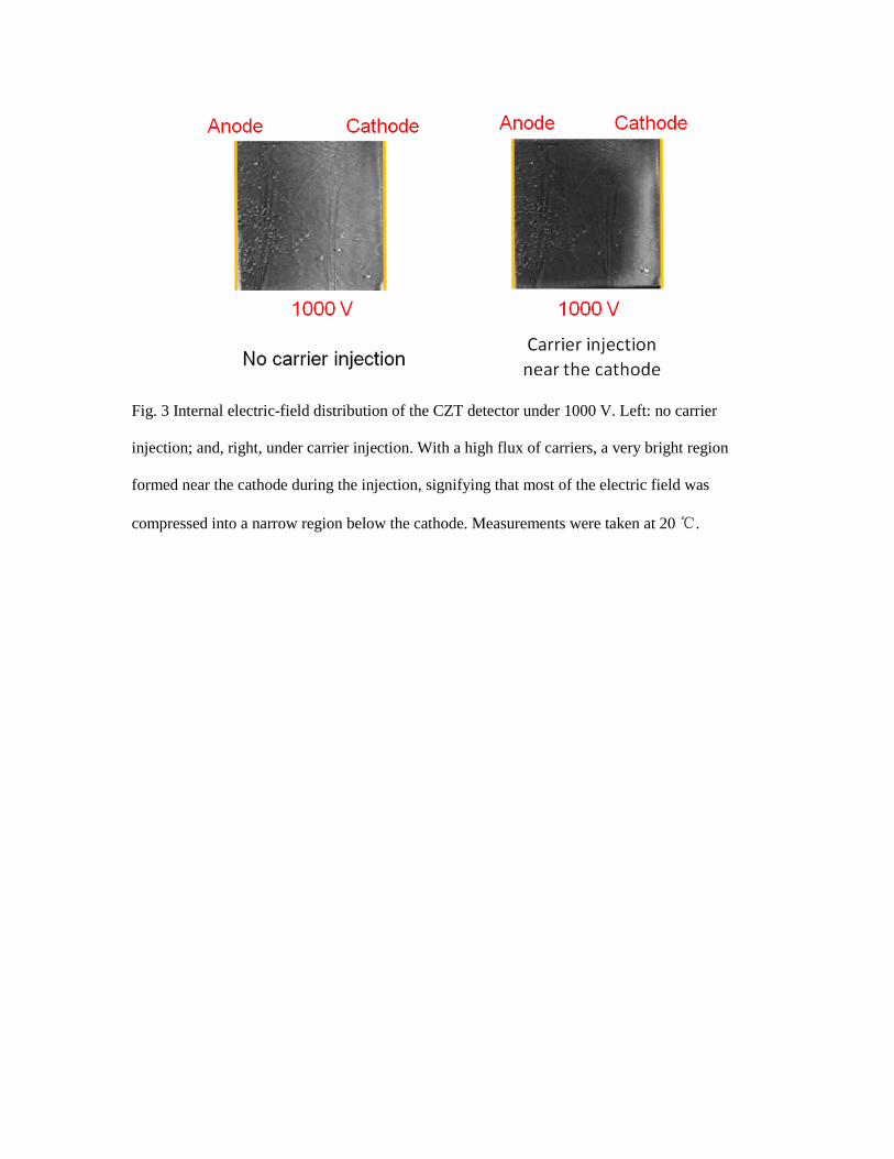
Fig. 3 Internal electric-field distribution of the CZT detector under 1000 V. Left: no carrier
injection; and, right, under carrier injection. With a high flux of carriers, a very bright region
formed near the cathode during the injection, signifying that most of the electric field was
compressed into a narrow region below the cathode. Measurements were taken at 20 ℃.

Fig. 4 Change of photocurrent during the high flux of carrier injection. The measurement
temperature was 20 ℃.

Fig. 5 Internal electric-field of the CZT detector under high flux carrier injection at 5 ℃, 20 ℃
and 35 ℃. The uniformity of the field improved markedly with increasing temperature.