international conference on multidisciplinary research ... · hardware implementation of mlp and...
TRANSCRIPT

International Conference on Multidisciplinary Research & Practice P a g e | 132
Volume I Issue VII IJRSI ISSN 2321-2705
Hardware Implementation of MLP and RBF Neural
Networks onto Multiple Processing Nodes
Tejas Dalal
Dhirubhai Ambani Institute
of Information and Communication Technology,
Gandhinagar, India
Mazad Zaveri
Dhirubhai Ambani Institute
of Information and Communication Technology,
Gandhinagar, India
Abstract — In this paper, describe an architecture consisting of
multiple Processing Nodes (PNs) for emulating/implementing
Artificial Neural Networks (ANNs). Our architecture can be
configured for implementing two types of ANNs (MLP and RBF).
Our architecture has a connection memory that can be configured,
in terms of the number of layers, and in terms of the inter-layer
connectivity requirements. When compared to the existing CNAPS
architecture, our architecture does not require the inter-PN buses,
leading to a reduction in the communication time, and the area.
Our architecture is based on <8, 6> fixed-point number
representation. Our architecture (applied to an example
recognition task using Iris dataset) has been
implemented/synthesized on two 45 nm technology based
platforms (ASIC and FPGA), and results have been provided,
indicating that an ASIC implementation is more advantageous in
terms of area/speed/power.
I. INTRODUCTION
The human cortex is a complex and fast computing machine.
Memory, thought process, problem solving, and decision
making capabilities of the cortex have inspired researchers to
invent mathematical/computing models that are able to do
similar operations, and are referred to as Artificial Neural
Networks (ANNs). Such models capture the cortex’s function at
the most fundamental level (neural-level of abstraction [1]). A
neuron is a basic cellular unit of the cortex, and each neuron
can be approximated as a simple processing unit, which
receives and combines several signals. The basic model of an
artificial neuron is shown in fig.1.
The generalized architecture of ANN, generally consists of
several Processing Nodes (PNs), where each PN could emulate
one or more neurons [1]. A PN (emulating one neuron) has
several inputs, and combines it usually by a simple summation.
The output of a PN can be the input of other PNs through
weighted connections, which correspond to the strength of
synapses.
The most challenging applications of ANNs are: hand written
character recognition, function approximation, time series
prediction, control systems, etc.
II. ARCHITECTURE OF ANN The architecture of ANN is shown in fig.2, where, several PNs
are connected via shared bus through a control block, which
takes all decisions, required for communication between PNs.
Our proposed system architecture is based on the regional-
broadcast scheme suggested in [1], and the ANN
implementations in [2]. The internal architecture of each PN is
shown in fig.3.
Fig. 1. Architecture of Artificial Neural Network
Fig. 2. Architecture of ANN

International Conference on Multidisciplinary Research & Practice P a g e | 133
Volume I Issue VII IJRSI ISSN 2321-2705
A. Activation Functions
Two activation functions have been implemented:
1) Sigmoid function for Multilayer perception (MLP) neural
network 2) Gaussian function for Radial Basis Function (RBF) neural
network
Fig. 3. Architecture of PN
The former function is a logistic function that ranges from 0 to
1, and is similar to hyperbolic tangent function, which ranges
from -1 to 1. Therefore the input range is bounded in the range
of [-2, 2] and that can be represented using <8, 6> fixed-point
representation, where 2 bits are needed for the integer part and
remaining 6 bits are for fraction part, providing an accuracy of
approximately 0.0015625.
1) Sigmoid (activation) function for Multilayer
perception (MLP) neural network: The architecture of
activation function for MLP network is shown in fig.4. The
Exponential function can be implemented, in hardware, using
Piecewise Linear approximation (PWL) algorithm [3], [4]. The
multiplication and the exponential function can be
approximated using shifter and adder as shown in Table I. One
output is chosen from the three different shifters which are
controlled by the range of the input.
TABLE I IMPLEMENTATION METHOD
operation condition Flags
z1 z2 z3 z4
Y = 1 ||X|| 5 0 0 0 1
Y = 0.03125*||X|| + 0.84375 2.375 < ||X|| < 5 0 0 1 0
Y = 0.125*||X|| + 0.625 1 < ||X|| <2.375 0 1 0 0
Y = 0.25*||X|| + 0.5 0 < ||X|| <1 1 0 0 1
Y = 1-Y ||X|| <0
2) Gaussian (activation) function for Radial Basis
Function (RBF) neural network: The Gaussian function for the
RBF network has been implemented using Look up Table
(LUT). The input to this function is the distance of the input
vector from the stored center. This distance can be linearly
Fig. 4. Architecture of activation function for MLP network
mapped to the output.
The input to the activation function can be treated as the
address for the LUT. The LUT contains the output
corresponding to the input (or address), which is actually
obtained by discretizing the Gaussian curve, into (output, input)
pairs. As the range of the RBF output is bounded in the range of
[0, 1], it is easy to make such table, by simply dividing by 2width
.
Fig. 5. Architecture of activation function for RBF network
For 8 bit width, the difference between two subsequent
elements of the table will be 1/256 = 0.0039; in other words, the
range [0, 1] of the output is divided in 256 steps.

International Conference on Multidisciplinary Research & Practice P a g e | 134
Volume I Issue VII IJRSI ISSN 2321-2705
III. EXISTING ARCHITECTURES OF ANN
The approach of using (single) PN was introduced in ANNA
chips [5]. The architecture of ANNA chips is shown in fig.6.
Later on, multi-PN approach was shown in CNAPS [6], which
consisted of 65 PNs. The architecture of CNAPS is shown in
fig.7. A. ANNA Chips
ANNA stands for Analog Neural Network Arithmetic and
logic unit. A neural network for handwritten digit recognition
was implemented with 136000 synapses on a mixed
analog/digital chip. It was reported that, ANNA chips could
recognize 1000 characters per second, with an error rate of 5%
with floating point precision.
Fig. 6. Architecture of ANNA chips
ANNA chips was implemented on a 0.9 µm CMOS
technology. It implemented 4096 physical synapses, which
could be multiplexed. Resolution of the weights/synapses was 6
bit, and that of the input/output was 3 bit. All inputs/outputs of
the chip were digital, while the internal computation technique
was analog. The optical character recognition (OCR) algorithm
required four layers, and each layer was computed sequentially.
B. CNAPS Architecture
CNAPS architecture had an array of processors (or PNs).
These PNs were interconnected by three buses:-
1) PNCMD bus: broadcast the instruction from the
sequencer to the PNs.
2) IN/OUT bus: broadcast data from one PN to all the PNs
(8 bit wide).
3) INTER-PN bus: transfer data from each PN to one of
itsnearest neighbors (2 bit wide).
Fig. 7. Architecture of CNAPS
CNAPS network has layers, which are 1D or 2D structures.
Two 2D layerscould be connected locally. A2D and a 1D layer,
or two 1D layers could be fully connected. A simulation was
reported on CNAPS with 128 PNs, working at 20 MHz clock. C. Comparison of the Architectures
Comparison of our proposed architecture with the
conventional architectures (ANNA chips, CNAPS) can be
based on the following aspects:-
1) Topology - Both ANNA and CNAPS architectures have
fixed topologies. In our architecture, one connection
memory was introduced, which can be configures to
implement different topologies.
2) Requirement of buses –In our architecture, all PNs
communicate to each other only through the shared bus
via control unit. Hence our architecture does not require
the inter-PN bus (required in CNAPS).
3) Type of networks implemented -Both ANNA and CNAPS
architectures have a single activation function and
network (i.e. MLP neural network), whereas in our
architecture the activation function and the
networkisconfigurable as either MLP or RPF neural
network.
4) Type of chip that used -ANNA chips was based on mixed
analog/digital signals, whereas CNAPS and
ourarchitecture are based on fully digital signals.
IV. FUNCTIONAL VERIFICATION BY IMPLEMENTING
AN EXAMPLE
A recognition/classification example based on Iris
datasetwas implemented on our architecture using 4 PNs, as
shown in fig.8. This example, (as shown in fig. 9) requires 12
neurons in the hidden layer and 3 neurons in the output layer. A
total of four PNs were assumed, hence each PN would have 3
neurons in hidden layer (indicated by phase 0in connection
memory) and 1 neuron in output layer (indicated by phase 1
inconnection memory).
International Conference on Multidisciplinary Research & Practice P a g e | 135
Volume I Issue VII IJRSI ISSN 2321-2705
All 15 (=12 + 3) neurons have been equally distributed (as
shown in fig. 10), across the PNs. Each PN hasthe same number
of neurons to be emulated, and hence, takes the same amount of
time for computation (for each layer), eliminating the need for
any PN to wait, before the communication starts.
Fig. 8. Implementation of the Iris example, using 4 PNs
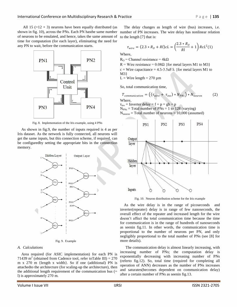
As shown in fig.9, the number of inputs required is 4 as per
Iris dataset. As the network is fully connected, all neurons will
get the same inputs, but this connection scheme, if required, can
be configuredby setting the appropriate bits in the connection
memory.
Fig. 9. Example
A. Calculations
Area required (for ASIC implementation) for each PN is 71439 m
2 (obtained from Cadence tool, refer toTable III) = 270
m x 270 m {length x width}. So if one (additional) PN is attachedto the architecture (for scaling-up the architecture), then the additional length requirement of the communication bus (= l) is approximately 270 m.
The delay changes as length of wire (bus) increases, i.e.
number of PN increases. The wire delay has nonlinear relation
to the length [7] that is:
𝜏𝑤𝑖𝑟𝑒 = 2.3 ∗ 𝑅𝑂 + 𝑅𝑙 𝑐𝐿 = 2.3 ∗ 𝑅𝑂
𝑅𝑙+ 1 𝑅𝑐𝐿2(1)
Where,
RO = Channel resistance = 4kΩ R = Wire resistance = 0.08Ω {for metal layers M1 to M3} c = Wire capacitance = 4.5-3.5aF/λ {for metal layers M1 to M3} L = Wire length = 270 µm
So, total communication time,
𝑇𝑐𝑜𝑚𝑚𝑢𝑛𝑖𝑐𝑎𝑡𝑖𝑜𝑛 = 𝜏𝑤𝑖𝑟𝑒 + 𝜏𝑖𝑛𝑣 ∗ 𝑁𝑃𝑁𝑠 ∗ 𝑁𝑛𝑒𝑢𝑟𝑜𝑛 (2) Where, τinv = Inverter delay = f + p = gh + p NPNs = Total number of PNs = 1 to 128 (varying)
Nneuron = Total number of neurons = 10,000 (assumed)
Fig. 10. Neuron distribution scheme for the Iris example
As the wire delay is in the range of picoseconds and
inverter(repeater) delay is in range of few nanoseconds, the
overall effect of the repeater and increased length for the wire
doesn’t affect the total communication time because the time
for communication is in the range of hundreds of nanoseconds
as seenin fig.11. In other words, the communication time is
proportional to the number of neurons per PN, and only
negligibly proportional to the total number of PNs (see [8] for
more details).
The communication delay is almost linearly increasing, with
increasing number of PNs; the computation delay is
exponentially decreasing with increasing number of PNs
(referto fig.12). So, total time (required for completing all
operation of ANN) decreases as the number of PNs increases
and saturates(becomes dependent on communication delay)
after a certain number of PNs as seenin fig.13.

International Conference on Multidisciplinary Research & Practice P a g e | 136
Volume I Issue VII IJRSI ISSN 2321-2705
B. Results and Discussions
70% of the Iris datasetwas used for ANN training, and testing
was done on the remaining 30%. For the Iris example, the
estimatedtotal simulation time (computation + communication
delay) = 12 + 12 + 12 = 36cycles, where cycle time is 50ns
(corresponding to frequency of 20MHz). So, simulation time =
36 x 50ns = 1800ns, and Total # of Connections (synapses) 12 x
4 + 3 x 12 = 84.So the speed, in terms of Connections Per
Second (CPS), of our architecture is64 / 1800 ns = 46.66
MCPS.
1) Matlab®
Results:NNtoolinMatlab®
was used to obtain
the trained weights for both the (MLP and RBF) neural
networks. Training was done for 1000 iterations, with an error
in the range of 10-6
. The results that were obtained from the
Matlab® were converted into <8, 6>fixed-point representation,
for comparing them to the results obtained from the behavioral
and synthesized HDL implementations.
Fig. 11. Wire delay v/s number of PNs
Fig. 12. Computation and communication delay v/s number of PNs
Fig. 13. Comparison of speed (ANNA chips, CNAPS, our architecture) different number of PNs
2) FPGA Results: The HDL code for the Iris example, was
successfully synthesized using Xilinx tool, for a Spartan 6
FPGA board (45 nm technology). This implementation is
capable of performing with the speed of 131.68 MCPS for an
architecture with 4 PNs. If the number of PNs (running in
parallel) increase, the speed can be further improved
3) Cadence Results: The result has been obtained for
45nm technology with nangate opencell slow library. For
synthesis, RTL complier tool was used, and for physical
layout/designing encounter tool was used. The results, obtained
from Cadence tools are given in Table II, Table III, and Table
IV. Also final layout is shown in fig. 15.
Fig. 14. FPGA functional verification
TABLE II
AREA RESULT FROM CADENCE
Type Area ( m2) Area (%)
Cell Area 101646 35.89 % Net Area 181566 64.11 %
Total Area 283211 100 %
TABLE III POWER RESULT FROM CADENCE
Type Power (mW) Power (%)
Leakage Power 1.286 mW 30.30 % Dynamic Power 2.958 mW 69.70 %
Total Power 4.243 mW 100 %
TABLE IV RESOURCE UTILIZATION RESULT FROM CADENCE
Type Instances Area (um
2) Area (%)
Sequential 23272 68579.06 67.46 Inverters 5823 3220.20 3.20 Logic 22058 29856.26 29.35 Total 51153 101645.52 100
Average Fan-out 2.0

International Conference on Multidisciplinary Research & Practice P a g e | 137
Volume I Issue VII IJRSI ISSN 2321-2705
Fig. 15. ASIC Layout
4) Comparison of Results with the Existing Architectures of
ANN:When compared to CNAPS, our architecture (which has a
connection memory) provided more speed without extra cost in
terms of area (i.e. inter-processor buses in CNAPS). Data displayed
in the Table V has been adapted (and appropriately scaled) from
[5] and [6]. From Table V, our architecture is 2x faster than
CNAPS, while slower than ANNA chips (for obvious reason, that
in ANNA chips, the multiply-summation operation is happening in
parallel in the analog domain). The results given in Table VI, are
for 4 PNs, so if more PNs run in parallel, then it is obvious that the
speed advantage will be much more.
5) Comparison of the ASIC and FPGA platform:Comparison of
the results for the two platforms are shown in Table VII, which
shows that the ASIC design is much faster, less power consuming
and requires less area, but the drawback of ASIC is high
designing/manufacturing cost.
TABLE V COMPARISON OF RESULTS
Speed Activation
(MCPS) Function
Implemented
CNAPS (128-PNs) 20MHz 153.2* MLP
ANNA Chip 2624.0* MLP
This Architecture (4-PNs) 20MHz 46.66 MLP, RBF
This Architecture (128-PNs) 20MHz 1294.33
* values with appropriate technology scaling
TABLE VI COMPARING TWO PLATFORMS
ASIC (Cadence) FPGA platform
Power 5.36 mW 26 mW Speed 353.53 MCPS 171.56 MCPS
Area 283211 µm2 1280000 µm
2
We can conclude that, the ASIC design can be implemented
for very larger-scalearchitectures, where power, speed and area
have higher priority, and when extremely large number of PNs
are required (justifying the mass production and related
manufacturing costs). FPGA can be used as an alternative to
ASIC for small-scale architectures, where re-configurability has
a higher priority than power, speed or area.
REFERENCES [1] M. S. Zaveri and D. Hammerstrom, “Performance/price estimation for
cortex-scale hardware: A design space exploration,” Neural Networks, vol. 24, no. 3, pp. 291–304, Dec 2010.
[2] N. B. Ambasana and M. S. Zaveri, “Analysis of increased parallelism in fpga
implementation of neural networks for environment/noise classification and
removal,” Nirma University International Conference on Engineering,
Ahmedabad, India, Dec 2012. [3] H. Amin, K. M. Curtis, and B. R. Hyes-Gill, “Piecewise linear approximation
applied to nonlinear function of a neural network,” in IEEE proceeding -
Circuits Devices Systems, vol. 144, no. 6, Dec 1997, pp. 333–317. [4] N. B. Ambasana, “FPGA implementation of neural networks for
environment/noise classification and removal,” Master’s thesis, DA-IICT, Gandhinagar, India, 2012.
[5] E. Sackinger, B. E. Boser, J. Bromley, Y. LeCun, and L. D. Jackel, “Application of the anna neural network chip to high speed character recognition,” IEEE Transaction on Neural Networks, vol. 3, no. 3, May 1992, pp. 498–505.
[6] B. Granado and P. Garda, “Evaluation of cnapsneuro-computer for the simulation of mlps with receptive fields,” in Proceedings of TWANN, 1997.
[7] D. Zhou, F. Preparata, and S. M. Kang, “Interconnection delay in very high
speed vlsi,” IEEE Transaction on Circuits and Systems, vol. 38, no. 7, pp.
779–790, July 1991. [8] Tejas Dalal, “HDL Implementation and study of Artificial Neural
Networks, Mapping onto multiple Processing Nodes” Master’s thesis, DA-
IICT, Gandhinagar, India, 2014.