international efficiency challenge electric vehicle
TRANSCRIPT

INTERNATIONAL EFFICIENCY CHALLENGE
ELECTRIC VEHICLE
TECHNICAL DESIGN REPORT
Deadline: August 4th, 2021
VEHICLE AND TEAM NAME: BURST
UNIVERSITY: BOGAZICI UNIVERSITY
ACADEMIC ADVISOR, IF ANY: NURI BULENTERSOY
TEAM CAPTAIN: ESMA SAHIN
VEHICLE TYPE: ELECTROMOBILE HYDROMOBILE

CONTENT
1.Vehicle Specifications Table ............................................................................................................ 3
2.Vehicle Dynamic Testing .................................................................................................................. 4
3.Domestic Sub-Components ............................................................................................................. 4
4.Motor ................................................................................................................................................... 5
5.Motor Driver ........................................................................................................................................ 6
6.Battery Management System (BMS) ............................................................................................ 25
7.Embedded Recharging Unit ........................................................................................................... 29
8.Battery Packaging ........................................................................................................................... 32
9.Vehicle Control Unit (VCU) ............................................................................................................ 35
10.Insulation Monitoring Device ....................................................................................................... 39
11.Steering System ............................................................................................................................ 42
12.Door Mechanism ........................................................................................................................... 46
13.Mechanical Details ........................................................................................................................ 47
14. Vehicle Electric Scheme .............................................................................................................. 56

1. Vehicle Specifications Table
Feature Unit Value
Length mm 3000
Width mm 1360
Height mm 1400
Chassis material Aluminium and Carbonfiber
Shell material Carbonfiber
The brake system hydraulic disc, front, rear, hand brake
hydraulic disc
Motor type BLDC
Motor driver self-designed, ready-made product
self-designed
Motor power kW 1.5
Motor efficiency % 89
Engine weight kg 16
Battery type Li-ion
Battery pack nominal
voltage
V 59.2
Battery pack
capacity
Ah 25.3
Battery pack
Maximum voltage
V 67.2
Battery pack energy Wh 1506
Fuel cell power kW -
Number of hydrogen cylinders
# -
Hydrogen cylinder pressure
bar -
Super capacitor yes/no -

2. Vehicle Dynamic Testing
3. Domestic Sub-Components
1. Motor Mandatory for Electromobile/Hydromobile
2. Motor driver Mandatory for Electromobile/Hydromobile
3. Battery management system (BMS)
Mandatory for Electromobile/Hydromobile
4. Embedded recharging unit Mandatory for Electromobile
5. Energy management system (EMS)*
Mandatory for Hydromobile
6. Battery packaging Optional
7. Electronic differential application Optional
8. Vehicle control unit (VCU) Optional
9. Fuel cell* Optional
10. Fuel cell control system (circuit)* Optional
11. Insulation monitoring device Optional
12. Steering system Optional
13. Door mechanism Optional
* Hydromobile category only

4. Motor
Determination of motor type
Motor type selection is done after considering the advantages of three motor types,
which are brushed DC motors, brushless DC (BLDC) motors, and induction motors.
Brushed DC motors suffer from friction of brushes, which reduces life and efficiency of
the motor. Also due to friction, brushed DC motors may heat up excessively during
operation. However, they do not require a controller or a simple controller is sufficient
for them. Induction motors, on the other hand, do not have any permanent magnet
and spend energy for magnetising, which leads to efficiency loss. They are better than
brushed DC motors in overall efficiency but require a rather complex controller. BLDC
motors are way more efficient than brushed DC motors since they do not suffer from
brush friction. Moreover, thermal characteristics are better than brushed DC motors
because of the lack of brush friction. They require more complex controllers than
brushed DC motors but the controller they need is often simpler than induction motors.
In VECTOR, a hub BLDC motor is used. Hub motors are easier to implement since
they do not require any power transmission to the wheels. Considering these, it is
decided that for VECTOR a BLDC hub motor is used.
Determination and calculation of motor parameters (shaft torque and
speed, power, voltage, current, weight etc.)
The main parameter for motor selection was the cost. An 1.5 kW 70V hub motor
with 16 inch diameter rim was found in the online market, which was economically
feasible. After purchase stall torque is calculated by loading weight that produces
torque against the motor. It was found to be around 80 Nm. The weight of the motor is
calculated to be 16 kg.
Determination and calculation of motor dimensions
Hub motor is decided to be the best choice. Therefore, a hub motor with a 16
inch diameter rim is chosen to be in regulation with the Efficiency Challenge rules.

5. Motor Driver
1.Introduction
BLDC motors are composed of two main parts which are stator and rotor. The stator
part includes coils and the number of coils determines the pole number of the stator.
Generally, these coils consist of three phases which are arranged in a certain
sequence. The rotor part involves permanent magnets which are arranged in a
sequence of opposite poles consequtively. It is placed either inside or outside the
stator. Apart from rotor and the stator, to determine the position of the rotor, some
BLDC motors include hall effect sensors. These sensors are placed on near the rotor.
They provide a logic output according to the pole of the permanent magnet they are
currently seeing. The internal structure of a typical BLDC motor is shown in Fig.1.
2.Objectives
We are planning to design an embedded power board that can drive a 2kW (peak
20kW) BLDC motor. This board will be able to control the speed of the BLDC motor
with a PWM signal. This board will also allow the motor to rotate in the desired direction
( forward and backward ).

As stated above, to design an efficient BLDC motor driver, the internal structure of the
BLDC motor must be well known. As can be seen in Fig.2, a BLDC motor is composed
of three different windings in the stator and permanent magnets in the rotor. To drive
these types of motors, the coils must be energized in a synchronous manner. These
synchronization can be achieved with an external driver circuit which includes power
MOSFETs and a control circuitry as shown in Fig.2. The switching operation for
synchronization is performed by 6 power MOSFETs which are controlled by an external
circuitry. In this project, we will design a BLDC motor driver circuitry that can perform
these switching operations efficiently.
The main problem about driving a BLDC motor is the imperfection in switching timing.
The perfect timing for switching operation is related to the speed and current position
of the motor. For the smooth operation of the BLDC motor, speed and current position
of the motor should be known precisely. Hall effect sensors, which are able to read the
speed and position of the rotor, are generally used in BLDC motors. Thus, we are going
to drive the MOSFETs with perfect timing according to the data comes from the hall
effect sensor.

3.Approach and Methodology
This project basically consists of three main stages:
Gathering technical background information
According to these technical backgrounds designing the main board
Tests and improvements
3.1 Six-Step Commutation
Unlike physical commutation in DC motors, we have to drive the BLDC motor with
solid state commutation which is composed of six steps. As mentioned in the
introduction part, the coils inside the motor will be energized synchronously. To achieve
this synchronization, we have to know the exact position of the motor. Since the
rotation of this motor is relatively slow, we cannot use back EMF to detect the speed
and position accordingly. Thus, three hall effect sensors, which are sensing switches
that output a logic level base on the magnetic field detected, are inserted into the stator
of the motor. By using the outputs of these sensors, the position of the motor and
switching time will be determined. For example, when the Ha is under the effect of N
pole of the permanent magnet, it will output logic level 1, otherwise 0 as can be seen
in Fig. 3.
According to the outputs of these hall effect sensors, at the each step one of the
phases will be connected to VDD and one of them will be connected to the ground. The
sequence of the switching operations is presented in Table I and visually depicted in
Fig. 4.

This commutation table is for the forward rotation of the motor. In order to rotate the
motor backwards, the phases will be reversed.
3.2 Power MOSFET and 3-Phase H-Bridge

Since the operation principle of the BLDC motors resembles an AC motor, we have
to convert DC to a square wave AC signal. To do that, we will use a 3-phase H-
bridge configuration composed of six MOSFETs as shown in Fig. 5. Since this is a
high power project, we should use power MOSFETs.
In this H-Bridge configuration, to supply a square wave AC signal to the motor
according to the six-step commutation sequence indicated in Table I, one of the
upper MOSFETs and one of the lower MOSFETs should be switched on at a
particular time. Thus, one of the phases of the motor will be connected to VDD and
one of them will be connected to ground according to the hall sensor’s outputs. In
order to deliver high power to the motor, we should use power MOSFETs. The
selection of the appropriate MOSFETs will be explained in part 4.1.
3.3 Gate Drivers

The purpose of the gate drivers is to supply sufficient current to the gates of the
MOSFETs in order to switch them. For small sized MOSFETs, it is not required to have
gate drivers because their gate capacitances are very small and even a low amount of
current is enough to switch these small sized MOSFETs. Most microcontrollers operate
at 5V or 3.3V and can output this small amount of current. However, since we will use
power MOSFETs whose sizes are very large, they will demand high gate currents for
switching. Therefore, we are going to need gate drivers as an intermediate step
between the microcontroller and the MOSFETs.
4.Work Completed
4.1 Component Selection
We have studied the basic working principles of the BLDC motors and how to drive
them properly. According to these researches we have done, we recognized that the
output stage of the driver must include 6 MOSFETs, each two of them is placed in a
half-bridge configuration, in order to supply sufficient power to the motor. Since we are
designing a high power BLDC motor driver board, we started to search a proper
MOSFET model that satisfies our specifications. These specifications are listed below.
The Maximum Current MOSFET can Withstand (ID): Since the power level of
the BLDC motor we are going to drive with this board is quite high ( nominal
2kW, peak 20kW), the motor will draw so much current. Since the board will
operate with around 70V, the peak current would be approximately 285A. Thus,
the maximum current that passes through the MOSFET without damaging it is
important.
Maximum VDS Voltage: As the motor we are going to drive operate with around
70V, the maximum drain-source voltage of the MOSFETs, which are in cut-off,
is also 70V. Therefore, the MOSFETs should properly operate in this voltage
level without any damage. Moreover, to avoid any damage due to the possible
voltage spikes, we decided to leave at least 15V margin.
RDS-ON: As mentioned above, operating current level is high. Hence, drain to
source resistance when the transistor is on must be pretty low in order to prevent
high voltage drops over the MOSFETs. Moreover, to minimize the power loss
and heat dissipation, we should select RDS as low as possible.
Input Capacitance (CIN): Input capacitance determines the maximum
frequency of the switching operations of the MOSFETs. We are planning to
switch the MOSFETs with around 30kHz PWM signal to adjust the speed and

torque of the motor. The period for this frequency is 33.33µs. Therefore, the
switching delay of the MOSFETs should be much lower than this delay(one
hundredth of 33.33µs is quite sufficient). Calculation of the maximum input
capacitance for this specification is shown in Eq. 1 and Eq. 2.
Figure 6-7. Eq1 and Eq 2
Thus, the input capacitance value must be lower than half of this Cmax value due to
parallel configuration of two MOSFETs.
Since none of the MOSFETs presented in Table II cannot withstand peak current of
285A, we decided to connect two MOSFETs in parallel (in total 12 MOSFETs).

According to Table II, the most appropriate MOSFET is IRF100P219 so we decided to
select it among the others.
After selecting the MOSFET, we moved on choosing the appropriate MOSFET
driver. The specifications for the MOSFET driver are listed below.
Output Current Capability: It is crucial to choose appropriate gate driver that
can supply sufficient current to the gates of the MOSFETs in the design of motor
drivers. How fast the MOSFETs can turn on depends on the amount of current
supplied by MOSFET driver. Calculation of minimum required gate current is
indicated below.
Figure 8. Current Equations
According to the calculation 0.86A current capability is enough. However,
increasing the output current of the drivers will lower the propagation delay so the
efficiency will be improved.
Propagation Delay: Propagation delay is the amount of time it takes for the
signal from input to output. As stated previously, propagation delay of the
MOSFET driver must be lower than 333.3ns.
According to these specifications, we decided to use IR2110 MOSFET gate driver
whose output current capability is 2A and propagation delay is typically 94ns.

4.2 Design Process
According to the researches and investigations of datasheets of the different
components, we drew a pre-design schematic. In this schematic, since there is not
a BLDC motor model in LTspice, we modeled it with three inductors and three
resistors for the phases. We determined the phase resistance of the motor as 1Ω
which corresponds to 35A phase current because the nominal current of the motor
will be around that much. For the case of phase inductance values, we investigated
the datasheets of the typical 2kW sensored BLDC motors and found the inductance
value as 10mH.
Figure 9. Logic Schematic
We also modeled the hall effect sensor outputs as three square wave input signals that
are applied to the circuit externally. Additionally, the hall sensor outputs must be
analyzed and the input of the gate drivers must be determined according to them with
a microcontroller. However, we also do not have the model of microcontroller in
LTspice. Therefore, we modeled it as a combinational logic circuit whose truth table is
shown in Table III. Truth table is designed according to the commutation table
indicated in Table I.

Figure 10. Logic Table

In the preliminary design preliminary design, we thought that testing the circuit with the
2kW motor may result in some reliability and damaging problems. Therefore, we
decided to test our circuit with a low power sensored BLDC motor which is a CD-ROM
motor. The schematic of the design with Arduino is shown in Fig. 11.
Before setting up the test circuit, we tested the hall effect sensor outputs of the
CD-ROM motor. We observed the voltage level of the sensor outputs with the
oscilloscope and realized that voltage levels are not digital. After that, when we
investigated the CD-ROM motors, we noticed that there are two outputs for each phase
and they are analog signals. Thus, they should be put into a comparator to obtain digital
outputs for the microcontroller. Using three comparator, we tested the hall effect
outputs connecting each of them to an LED as shown in Fig. 12.

As can be seen in Fig. 12, hall effect outputs change depending on the position of the
rotor. After testing hall effect outputs, we set up the circuit in Fig. 11 in the electronics
laboratory and managed to rotate the motor with potentiometer speed input.

After simulating the circuit in Fig. 9, we obtained the simulation results shown in Fig.
14.
In this simulation results, we basically obtained the theoretically expected phase
voltage graphs. However, we observed some ‘inductive flybacks’ at the switching time
of the phase voltages. These inductive flybacks stem from internal inductance of the
coils. An inductor opposes the change in current and try to create a potential across
itself large enough to keep the flux at the same level. Therefore, this would cause the
polarity of the voltage across the inductor to reverse instantaneously. We realized that
we can solve this problem connecting relatively small resistances to phases.
Additional to these work completed in the first semester, we began this semester with
code improvements. The code we wrote in first semester didn’t have forward and
backward direction input and also the speed adjustment input included only three
stages. The first code was written to control the low powered BLDC motor, therefore
we made some improvements in the code.
To rotate the motor backward, we should connect the phases opposite to the forward
direction as can be seen in Table III. We defined an input for the motor direction in the
microprocessor. When it is high, the motor rotates backward; when it is low, the motor
rotates forward according to code.
The previous code consists of only three speed levels. In the new code, we
divided the speed levels into 160 levels to get continuous and smooth speed
adjustment.

In order to filter the fluctuations in the speed adjustment analog signal coming
from the potentiometer, we averaged each five samples. This average value
corresponds to duty cycle value of the PWM signals for the upper side MOSFETs.
As we have mentioned before, the previous code was written for low powered
BLDC motor. Since this motor rotates with very high RPM, the switching frequency for
the PWM signal should be quite high. However, since the switching frequency is
directly related with power loss and the high powered BLDC motor will rotate with
relatively slow RPM, we considered to decrease the switching frequency for the PWM
signal to 25 kHz. Besides, we could have reduced the switching frequency a little bit
below this value but we took into account that below 20kHz, there could be some
disturbing noises a human can hear.
After the code improvements, we continued with upgrading our test board for high
power tests. Since phase currents will be very high, we set up the high power part of
the circuit on a temporary PCB leaving the controller circuit on the breadboard as can
be seen in Fig. 17.

Before testing the circuit with high power motor, we tested with low powered motor to
observe the performance of power part of the circuit. The board could manage to drive
the motor smoothly in both direction at a given speed input.
After that, we went to the workshop to test our board with the original motor on the
car. Before the test, to prevent any damage we took some precautions such as adding
fuse to the batteries and emergency stop button. During the test, we were measuring
the temperature of the MOSFETs not to overheat them since we don’t have any heat
sink and cooling system yet. In the test process as it is shown in Fig. 18, the motor
did not rotate as we expected. At first it didn’t rotate smoothly and there were some
lock ups during rotation. In order to understand possible reasons, we controlled the
hall sensor outputs of the motor and we saw that hall effect outputs were very noisy.
Additionally, we considered that there might be high voltage oscillations in the phase
voltages as seen in the simulation results. Furthermore, since motor couldn’t rotate
properly, each of the phase voltages cannot be pulled down to ground and the
bootstrap capacitors cannot be fully charged. Thus, upper side MOSFETs cannot be
turned on properly due to low gate source voltage. Therefore, we go back to the design
process to solve these problems.
We begin with filtering the hall effect sensor outputs. The hall effect sensor output were
fluctuating when it is high or low which result in wrong measurements. To stabilize it,
we considered to put a low pass filter as shown in Fig. 19.

The value of the capacitor should be large enough to filter the noise and should be low
enough not to disturb switching operation. We figured out that 1nF might be a good
choice.
As we mentioned before another problem might be high voltage oscillations in the
phases. Since the internal inductance of the motor is very large, when the transistors
are switched off corresponding to that phase, the energy on the inductance cannot go
anywhere. We considered that adding a path to phases might solve this problem. After
that, we made some researches about this topic and found that “snubber circuit”
topology might eliminate this problem.
Snubber Circuit
A large part of the power loss in a transistor occurs during switching. This power loss
during switching can be reduced by snubber circuits and also this type of circuits can
protect the MOSFETs from switching stress of high voltages and currents.
A snubber circuit, whose typical schematic is shown in Fig. 20, changes the transistor
voltage and current waveforms to an advantage.

This snubber circuit provides another path for the phase currents during MOSFET turn
off. While the MOSFETs are turning off and voltage across it is rising, the snubber
diode is forward biased and the capacitor starts to charge. This capacitor decreases
the rate of change of voltage over the MOSFET and delays its voltage transition from
low to high. The capacitor charges to the final off-state voltage across the MOSFET
and remains charged while the MOSFET is off. When the MOSFET turns on, the
capacitor discharges through the snubber resistor and MOSFET [7]. In other words,
snubber circuit provides a path for inductance current during switching and it behaves
like an open circuit, thanks to the snubber capacitor, when MOSFETs are not
switching.
Figure 21. Snubber Capacitor Graphs

As shown in graphs, a small snubber capacitor results in the voltage reaching
the final-off state before the MOSFET current reaches zero, whereas larger
capacitance results in longer times for the voltage to reach final-off state. Also these
graphs show that when the capacitor value increases, power loss on MOSFETs
decreases.
Capacitor value is chosen such that when the MOSFET current reaches to zero, the
capacitor voltage reaches final-off state. This capacitor value can be calculated as,
For our circuit,

Assuming five time constants for complete discharge,
Figure 22. Final Schematic

6. Battery Management System (BMS)
a)Balancing Method
The balancing Method used in our BMS is passive balancing. Using a
MOSFET and a ceramic 5W 3.3R resistor, around 1.15A can be discharged
though a parallel stack if desired. The schematic of a single cell discharge
circuit is given in Figure 6.1.
Figure 23. Cell Discharging Circuit
To discharge a cell, a signal is sent by the microcontroller to the base of Q8.
This signal is then sent to a 4N36 optocoupler to ensure galvanic isolation of
the battery cells and the microcontroller. The optocoupler in turn biases a
power MOSFET IRLML2502 which discharges the cell through a 3.3R cement
resistor. If certain cells are above the lowest voltage cell by 0.1V, they are
discharged. To overcome high discharge currents (around 20 V if cells are
discharging) the number of discharged cells is limited to 1. If more than one
cell fits the threshold criteria, they are discharged alternatively with 3 second
intervals.
b) SOC Estimation Algorithm
SOC estimation is done using only OCV using in the article by Elmahdi
Fadlaoui, Ismail Lagrat and Noureddine Masaif. Which can be found on this
link.

c) Control Algorithm
As it has been discussed in the cell balancing section, the lowest cell is set as
a reference and the cells above the threshold are discharged. For fan control,
45 degrees has been chosen. After cells reach 55 degrees, the buzzer is
activated and at 70 degrees the BMS cuts all current to the circuit by activating
a relay.
d) Circuit Design
The BMS samples each cell separately using a 4067 4x16 multiplexer. Each
cell is read by using a 16:1 voltage divider. To minimize current through the
voltage divider, current only passes when the cells are sampled. To achieve
this another multiplexer is used to create sampling signals. A single cell
sampling circuit is given in Figure 6.2
Figure 24
When an input signal is given to the cell, Q111 and Q112 both activate which
connects the voltage divider to the circuit. This value is then fed to a
multiplexer which enables the microcontroller to measure the voltages one by
one. The output of the multiplexer is fed to a unity gain buffer to lower input
impedance of the signal. Lower impedance enables higher accuracy in ADC of
the microcontroller. There are two Atmega328P microcontrollers in the system.
One of these handles the monitoring and safety precautions of the BMS while
the other handles intra-vehicle communications with a CAN bus. These two
microcontrollers in turn communicates with each other using I2C. We use
DS18B20 temperature sensor for simple digital temperature readings. Safety
of the car is accomplished by driving a relay on the BMS which in turn drives a
more powerful relay to cut the power of the vehicle. All the data acquired by

the BMS (temperature, cell voltages, current ) are sent to the VCU using CAN
protocol.
Figure 25. De/Multiplexers for cell reading, cell sampling and balancing

e) Simulation Studies
Figure 26. Microcontroller cell voltages input signal
Figure 27. Balancing currents for arbitrary balance signal
f) Printed Circuit Studies
As our PCB’s have not yet arrives no simulation or studies are made on the
physical PCB.

Previous Design Current Design
Battery Packing Design :
Output Voltage : 67.2V
Output Current : 32A
Balancing Method (active or
passive)
: Passive
Circuit Design Type :
SOC Estimation Algorithm : OCV Only
Control Algorithm : Lowest cell referenced
Domestic or Not : Domestic
7. Embedded Recharging Unit
Figure 28. Overall schematics of embedded recharging unit
For our embedded recharging unit, we have decided to use Half-Bridge Push-
Pull topology. Half-Bridge Push Pull Topology enables us to support the power levels
required for our design. As we have a 67.2V max voltage battery, we have chosen to
have a current rating of 10A, which would make our embedded recharging unit to have

a power rating of 672W. However we are aware that some losses can occur in the real
life application and we would have a lower power rating than 672 W.
We have added optocouplers to isolate our switching circuit from the city power
line. These optocouplers provide the input voltages for the gate drivers and enable us
to safely perform switching operations.
For simulation purposes, we have firstly realized the transistors as switches. In
our simulations, we have seen that we could receive constant current and voltage
levels with switches, albeit with some fluctuations. When we updated them with
MOSFET and MOSFET drivers in our simulation program, we stumbled upon some
problems with signal acquisition. As such, we have tested a switch realization with
breadboard and have not stumbled into problems. As we determined that our power
MOSFETs can withstand the specifications of our circuit (IRFBC40LC) we continued
with our circuit design. Forisolation transformer, an ETD59 core with a ratio of
N1:N2=21:10 is used. In theory, a %100 duty cycle would have resulted in 155(10/21)
= 73.8 volts .In practice this is not possible because the serial connected MOSFETs,
Q1 and Q2, have to be switched with a time difference to avoid a short circuit of the
input supply. In this circuit, N2:N1 ratio is multiplied by a factor of 0.95, so that the
proposed value for N1/N2 includes a small margin which guarantees the
demagnetisation of the core. To obtain the battery's max voltage, a %91 duty cycle
should be used.
Our Arduino counter code for frequency of 50 kHz is;
Charger’s second part’s schematic is as seen below;

Figure 29. T_OUT is the output of the ETD59 transformer, L1 is the ETD34 coil.
In this part of the schematic, we are using diodes to rectify AC to DC. We are
using a low-pass filter formed by the inductor (COIL) and a capacitor (C1). The low-
pass filter produces the average value of Vout. Our inductor is made with ETD34 core,
with 12 turns. In continuous mode the output voltage depends only on the duty cycle
and the input voltage, it is load independent. The change in inductor current is also
load independent. The output current Iout is taken to be the average value of the
inductor current IL. To read current voltage of the circuit, a voltage divider of 1/16 made
with resistors is used to read voltage with our MCU.
Figure 30. Maximum and minimum values of current, output and input voltages are
as seen in the graphics [1].
References
[1]Heinz Schmidt-Walte, Ralf Kories. Electrical Engineering: A Pocket Reference, ed.
6th, 2003

Previous Design Current Design
Circuit Topology : Half-Bridge Push Pull
Power : 670W
Output Voltage Range : 67.2-71,4
Output Current Ripple : 1A
Input Power Factor :
Power Conversion
Efficiency
:
PWM Controller IC : Arduino UNO
Protection Circuits /
Components
: Varistor, Termistor
PCB Size : 23 cm x 28 cm
8. Battery Packaging
Type of Battery
One of the most commonly used batteries in EVs is 18650. It is a type of Li-ion battery.

Figure 31. A cylindrical cell Properties of Cell We are planning to use Power-Xtra PX18650 2500mAh product. It is 3.7V. Battery Capacity Needed Although our battery is 3.7 V at nominal voltage, it actually has 4.2 for maximum voltage. Low voltage is 3.5 V. Current rating: Current is dependent on the motor, and our motor will use 30A in nominal and 60A at maximum. Voltage Rating Nominal voltage is 59.2V, maximum voltage is 67.2 V, and minimum voltage is 56 V. Configuration The configuration of the battery is 16S11P. Power: We will be using 16 in series and 11 in parallel, adding up to 176 Cells in total. Each cell is 2500mAh,

2.5Ah*3.7V = 9.25 Wh 9.25*176 ~= 1506 Wh Cell Assembly We will use soldering to stabilize the cells in the package. Battery Size and Weight 48 grams for one cell. In total we will have between 9-11 kg battery package. We are expecting a 40cm by 50cm package for the battery. Cooling Unit We will use 2 fans to cool down the battery pack. These fans will be controlled by the BMS. Battery Package
The package is made from aluminium and covered with non-conductive paint. The battery management system will be placed on top of the aluminium casing.
Figure 32. Design of battery packaging

Figure 33. Real life photo of battery packaging
9.Vehicle Control Unit (VCU)
In Vector, CAN Bus protocol is used for communication. Thus, we aimed to reduce
the error rate without any cost in data transmission. CAN Bus als has the advantage
of being a distributed system CAN also provides tools for diagnosing and managing
possible errors with tools that the software covers. When the error occurs, instead of
shutting down the entire system, it shuts down the faulty unit due to its autonomous
structure. Since CAN is a message priority system, it decides which message to send
priority between units. Messages numbered on the CAN are transmitted according to
their priority order. While this method ensures that messages do not collide, it limits
the length of the communication line. Therefore, CAN nodes can be connected via a
40m bus with a data transmission rate of 1 Mbit/s. We can obtain many vehicle data
such as battery cell voltages, total energy consumption, instantaneous current,

odometry data, instantaneous vehicle speed, fault codes via the CAN Bus system.
Significant reduction in the weight of
the vehicle, faster operation
of the sensors and more
precise printing of the
information coming from the
car were important factors in
our preference for the CAN
Bus protocol among the
communication protocols.
Figure 34.
In the VCU design, ATmega328p, an
8 Bit, 20MHz microcontroller that is
widely used in projects. Atmega328p
has 32 KB ISP flash memory and is
capable of read-write actions. Also
provides enough digital and analog
pins. Atmega328p (U1 in PCB) is
used due to its low cost, high
availability, a broad developer
community and our familiarity with
the microcontroller. For CAN Bus,
MCP2515 and MCP2551 ICs are
chosen due their reliability and low
cost.
The VCU board has; 5 Analog, 3 PWM, 1 Digital, CANH, CANL, 12V, 5V and
ground are the pins used in VCU design. Analog pins are used for I2C
communication, reading voltages coming from the isolation device, controlling speed
using the data coming from the pedal. PWM pins are used for speed control and
automatic circuit breaking using emergency relays if needed. CANH and CANL pins
are for data transmission lines to communicate with other CAN Bus modules. VCU
also provides speed information for the motor driver.
Through CAN, VCU receives instantaneous speed, cell voltages, total energy
consumption, instantaneous energy consumption and remaining battery capacity).
Figure 34.

To inform the driver, the VCU communicates with an on board Raspberry Pi 3 via
I2C, then the BURST overlay on the LED screen in front of the driver provides the
information regarding the current state(speed, battery voltages, total energy
consumption, temperature and remaining battery capacity). I2C is a data
transformation method in which the data are transmitted with messages. To send a
command from a device to another similar device, we assign the sender device as a
master and the receiver device as a slave. They send their information and
commands with a simple wire, that is to say, no additional devices are needed, but
the information connection becomes weaker when the wire between them becomes
longer, therefore, we use I2C protocol when two microprocessors are close to each
other.
This figure shows how the message is transmitted during conversation.
Figure 35.
The VCU acts as an hub where information coming from the driver, motor driver,
BMS, and isolation device is considered and taken action off of.
In our car Burst Vector, for the telemetry system we use UDP protocols between
our computer and the Raspberry Pi 3B+ computer of the car. In the UDP protocol,
Vector and our computer which we use as a listener connect with a hotspot. Our
Raspberry Pi 3B+ uses a static IP and publishes data which is referred to as datagrams
to our computer in a network.Unlike the TCP, UDP has no handshaking protocols while
providing checksums to control integrity of the data. It is also faster because it doesn’t
need any transmission, which is crucial in our real-time application.
In UDP, sockets are a combination of the Port_ID and IP_address.Port_ID is a
16bit integer value and can take values between 0 and 65535. The IP_address we use
is a IPv4 32 bit value which typically looks like 192.168.x.xx. The socket is bound to
the endpoint of the data transmission and this enables multiplexing which is very
important in today's world because all of the 4.29 billion possible IP addresses are
assigned.

An UDP datagram has two sections namely header and data. Header has 4
fields and these fields are 16bits.These fields are Source port number,Destination port
number, Length and Checksum. In our Python code we use the “socket” library to deal
with how to fill these headers.
We have one python code for the listener and one python code for our
Raspberry Pi which uses Raspbian OS. We print the telemetry data and the datetime.
For the listener we use the code below:
For the server(Raspberry Pi):

We mentioned the telemetry as raw_input here but the telemetry data is taken from the
Vehicle Control Unit and is mentioned in that section. We use a 10 km range Wi-fi
antenna placed at our monitoring center.
Previous Design Current Design
VCU Functions : Speed, Telemetry,
Energy consumption
Controller IC : ATmega328P
Number of VCU I/O : 6/7, Total 13
Electronic Circuit
Design
:
Printed Circuit Design : To be received
Printed Circuit
Manufacturing
: Outsourced
Software Algorithm : PID Controller, SOC
Experimental Study :
Size (PCB / Box) : 7.5cmx11.8cm
10.Insulation Monitoring Device
For our measurements of high side and low side isolation we used different
topologies. To check for high side isolation problems a high common mode unity gain
differential amplifier is used as a current shunt. The topology of the high side can be
seen in Figure 12.1.

Figure 36. Circuit for high side insulation resistance
Relays in this circuit enable different sampling timing and durations for low and
high side resistance measurements. By alternating high and low side measurement,
interference is limited. When high side resistance is sampled, the relays activate and
resistors R5, R7 and R23 connect to the circuit. R22 is given as symbolic for the
insulation value and is not a part of the circuit. When value of R22(insulation
resistance) decreases, current across R23 increases which is then fed to the
microcontroller using a differential amplifier with high common mode voltage.

Figure 37. Output voltage versus insulation resistance
For low side resistance measurement, an instrumentation amplifier design has
been implemented to increase the input impedance of the operational amplifiers. The
topology of low side measurement can be seen in Figure 12.3.
Figure 38. Low side resistance measurement circuit
The relay serves the same purpose in this circuit as well. Chassis is connected
to the input of the instrumentation amplifier. Chassis also connected to the voltage
divider of R3 and R1. When the value of R9(which simulates the isolation resistance)
decreases, the resistance of the bottom half of the divider also decreases. As a
result, the input voltage decreases. The output is then fed into the microcontroller
which is part of the VCU. Output waveform can be seen in Figure 12.4. When the
resistance values are below a given threshold, the buzzer on the BMS is activated.
Since we did not race last year, the comparison table has been omitted.

Figure 39. Output voltage versus insulation resistance
11. Steering System
Ackerman Steering Geometry
The steering knuckle is designed according to the
Ackermann Steering Geometry. Therefore, the inside tire
will turn in a smaller circle than the outside tire to ensure
turning without slipping.

Figure 40 and 41 : Ackerman Geometry and Steering Knuckle
Additionally, the moment arm for the steering rod is designed long enough to
keep the steering force as small as possible. Calculations show that 14,53 degrees
should be used as the steering angle.
Steering System
Starting with an estimation of rotation needed, angles of rotation is determined.
Then, according to the Ackerman principle, steering in the rack and pinion system is
established. Because this vehicle is designed from scratch as an autonomous car, the
steering system is designed to function autonomously as well. Autonomous steering
conducted by a step motor linked to the pinion and linear potentiometer is used as
feedback. As the steering box, the 3D printed part is designed in SolidWorks
environment and printed in order to maintain a custom design with durability and
lightness. 3D parts also have the advantage of further modifying the design to the
optimum throughout the processes of design and manufacturing.
First we started as calculating the
steering force needed on the shaft, the
process started by calculating the force on
front wheels and the scrub radius. Scrub
radius is estimated to be 10.5cm and force
on a single wheel is estimated to be 245N,
with a friction coefficient of 0,7 required
force is 171N for a single wheel, 342N
total. With a 10cm moment arm, force on
the rack would be 360N.
Figure 42. Steering Box Assembly
We decided to use a small and common pinion for the rack to reduce torque, an
one modul, 24 tooth pinion on top of the rack, with its rotational axis coincident with a
70 tooth gear, then another 24 tooth pinion is used to reduce torque needed. In the
center of our steering pinion, the pinion we connect the steering wheel and the step

motor, the minimum torque needed to overcome steering forces is 1,65Nm, a rather
low number for both the driver and the motor.
For the 3D part designs, the primary focus is to make sure the gear system is
intact in their assigned places without compressing them, compressing would result in
high friction forces for the 3D parts to handle. To assure they are in the right places, a
two parts solution is used. One part is to assign their places and other is to keep them
in their places and to work as a lid. In the figure above, the first part and gear system
without the lid is seen. The lid makes sure the bearings are hard-fitted in their places
and don’t move, bearings then provide a defined position for the gear system. Then
gears would be screwed to the shafts going through the bearings, this means no force
of gears will be applied to the 3D parts as they will not be touching them. The shaft for
the larger gear and the pinion on the rack, has 2 nuts on its ends to make sure the
shaft's position will not go through changes.
Another design aspect is the friction between the rack and the 3D part. The
force applied to the sides and to the bottom of the rack compartment is negligible, but
it is best to avoid any friction, so a solution is to apply a thin layer of epoxy resin on the
inner surface of the 3D part to avoid the effects of friction and as a further application,
applying carbon-fiber to strengthen the 3D part is also a choice.
As for the turning radius of the car, we decided to go with 30 degrees of inner
wheel angle, as this is the bare minimum in the rules, the steering box can be altered
and change the turning radius if it is found to be not enough in the tests.
Figure 43 and 44. Gear Lid Removed

Figure 45. Bicycle Model
The bicycle model would have a minimum turning radius of 3,6 meters in the
current parameters. Outer wheel would have a 22,18 degrees angle.
Figure 46. Rack Movement to Achieve 30 Degrees of Wheel Angle
Current steering model with 14,5 Ackermann angle, would require a 72mm
horizontal movement of the rack to achieve 30 degrees of wheel angle.

12.Door Mechanism
Door hinges are door retention system
components which play a very important role
in the automobile as it holds the door of the
automobile in case of side impacts or rollover
accidents. Hinge is the assembly of
components connected to the door and body
of the vehicle, linked to each other and
capable of rotating around the same axis. We
use a ready-made hinge and door
mechanism in this vehicle.
Figure 47. Door CAD
Figure 48. Shell CAD

13.Mechanical Details
A. Technical Drawings
,
Figure 49. Technical Drawing
B. Strength Analysis
Roll cage strength is important in that the driver should be protected in the case of
rolling and crashing. So, in order to make the chassis strong but light we used
aluminum alloy 6063 T6. Front rollbar is 470 mm in length, back rollbar is 1020 mm in
length. So, the H value will be 1020-470=550 mm. The displacement value calculated
by SolidWorks static simulation is 2.648 mm which should be less than H/200 value.
H/200 is 2.75 mm, so the value holds.

Figure 50. Static Analysis of the Chasis
A. Energy Consumption
By considering the flow simulation results on the shell and internal frictional loss of
energy, we can calculate the overall energy consumption.
The drag force resulted from the 50 km/h velocity movement is 68.843 N. Lift force is
88.74 N. The air friction is calculated as 2.51 N.
Vehicle with one driver weights is approximately 200 kg. It is an approximation
because some parts of the shell are subject to change. In addition, rolling resistance
coefficient of asphalt on rubber is 0.015.
Considering the above data:
(200 kg x 9.81 m/s^2 -88.74 N) x 0.015 = 28.1 N is friction force on wheels.
Net force between wheels and asphalt = 96.943 N
Energy consumed = Net force x Displacement
= 96.943 N x 4000 m = 387.772 J
In the case for 6% slope, we should calculate the wheel friction in a different way.
Net force on slop direction = 117.72 N + 1844.28N x 0.015 = 145.4 N
Power of the motor = 50 km/h x net force on the slope direction = 2.02 kW

1.5 kW = maximum value of velocity x net force on the slope direction = 13.93
m/s
C. Outer Shell Production
Outer shell production is the most costly and detailed production process in terms
of vehicle production. Because it contains a lot of steps with big produces and details.
Model for the shell production is produced by using two dimensional CNC that can
cut 5 cm thick slices of the model body which are 61 slices in total. Then, the slices
are combined on a profile and the slices are trimmed of to achieve the desired
smooth model surface. The surface is covered with plastic that will keep the epoxy
resin from the Styrofoam material. This method makes the extraction of the shell from
the model way easier.
The shell production from this point is conducted by a company so we will include
the material list and costs. The method of production is by hand laying carbon fibre.
The strengthening parts such as PVC is added in a second layer just before cutting of
the doors and windows.
Polyester Paste 10 kg
Viky Mold Seperator 1 kg
PVA Liquid Mold Seperator
2 L
Felt FiberGlass 450 gr/m^2
60 kg
Multipurpose Polyester 18 kg
8
Fiberglass Fabric 500 gr/m^2
15 kg
Brush Appropriate Gel Coat
20 kg
Blue Pigment 1 kg
Akperox A60 MEK-P 5 kg
Cobalt %6 2 kg
Brush No.4 5
Wood 1
PVC Foam 5mm 10 m^2
Quick Adhesive 10
Polyester (PVC appropriate)
20 kg
80 Sandpaper 100
Polyester Filler Primer 10 kg
Acrylic Paint 5 kg
Labor 1
Most of the materials are supplied
by our sponsor so only the labor is
paid going to be paid by the team
money. Labor costs 15000 TL.

D. Cost Calculation
Material Amount Total
Price
(TL)
Calliper 2 380
Master Cylinder 2 119,99
Flat Steel 40*10 2 m 82,6
Steel Rod 1 m 53,81
Car Renting - 37,75
Shock Absorber 4 280
Spacer 12 60
Screws 20 60
Bolts and Nuts 20 35
Rack 1 169,92
Ball Joint 2 57,92
Logic Level Converter (3.3 V-5 V) 5 50,28
Rim 2 500
Decoupage 1 463,2
Suspension Wishbone 8 389
Brake Master Cylinder 2 300
Lathe- rod production - 150
Bolts 4 15
Workshop key 20

Cleaning Supplies 50
Water 1 15
MCP2515 CANBUS SPI
Communication Module
2 60,4
Mouser Electronics(Battery
Management Battery Stack
Monitor)
4 762,05
Özdişan(Can Controller ve
Transceiver)
4+4 168,21
Hub motor 1 2807
Aluminum 40*40*10 18 m 1194,16
Cable Stripper 1 62,49
Robotistan(Cable) 45,66
Robotzade(Cable) 44,67
Battery (16s 11p BMS circuit
battery)
5626,59
Vacumm Leak Proof Tape
Length:15m 130 C Grey
4 175,99
Vacuum Nylon FLM120 VS
120C/75mic/300cm
10 m 342,25
Infusion Vacuum Hose PE 10-
12mm
20 m 78,23
Infusion Net 135gr/m2 Blue
Width:150cm
30 m 792,07
Peel Ply Cloth 83 gr/m2 -plain
Width:152cm
45,6 m^2 847,23
MGS Lamination Epoxy Resin
RIMR 135
25 kg 3.422,54

EPIKURE CURİNG AGENT MGS
RIMH1366
7,5 kg 1.100,10
PoliproplenHoneycompC:8mm-
80kg/m3T:10mm120cmX250cm
3 1.716,16
Model Production and Material 1 5.900
Blue Pigment 1 kg 110
Cobalt 2 kg 202
Wood 1 550
PVC Foam 10 m^2 1100
Polyester 20 kg 1100
Polyester Filler Primer 10 kg 400
Acrylic Paint 5 kg 550
Labor(Shell Production) 1 15.000
Figure 51-52-53. Shock absorber- Calliper – Spacers for Wishbones
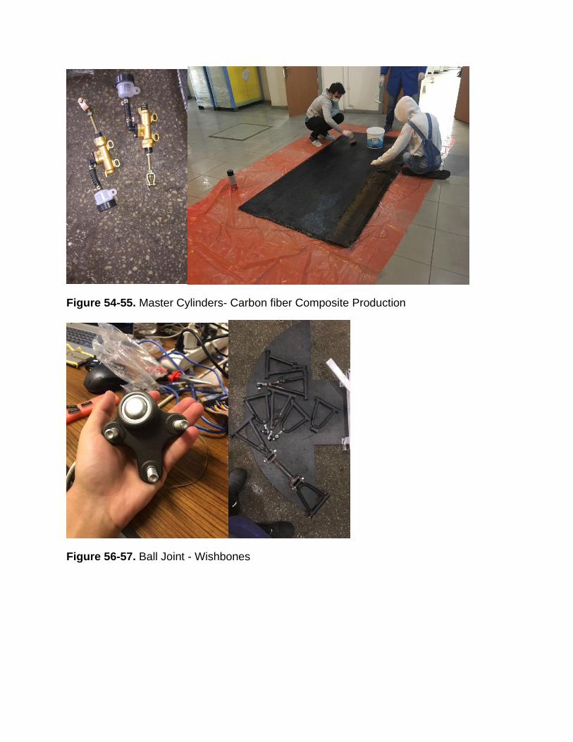
Figure 54-55. Master Cylinders- Carbon fiber Composite Production
Figure 56-57. Ball Joint - Wishbones

,
Figure 58-59. Styrofoam for Shell Model- Wishbone Assembly with Knuckle
Figure 60-61. Chassis Production with Al 6063 T6

Figure 62. Universal Joints

14. Vehicle Electric Scheme
Figure 63. Vehicle Electric Scheme

Figure 64. Vehicle Electric Scheme