international journal of management, it & … doc/ijmie_december/ijmra-mie738.pdfinternational...
TRANSCRIPT

International Journal of Management, IT & Engineering
(ISSN: 2249-0558)
CONTENTS Sr.
No. TITLE & NAME OF THE AUTHOR (S) Page
No.
1 Community Participation In Water Supply Schemes In Oke-Ogun Zone, Oyo State, NIGERIA.
Toyobo Adigun Emmanuel, Tanimowo N. Bolanle and Muili A.B 1-14
2 The current situation, future prospect of Poverty and inequality in Sudan.
Dr. Ali Musa Abaker and Dr. Ali Abd Elaziz Salih 15-31
3 Performance Evaluation of On-demand AODV and DSR Routing Protocols in Mobile Ad-hoc Network.
Muhammad Ashraf, Ahsan Raza Sattar, Tasleem Mustafa, Muhammad Inam Shahzad and Ahmad Adnan 32-57
4 Enhancement of Security for Initial Network Entry of SS In IEEE 802.16e.
Ahmad Adnan, Fahad Jan, Ahsan Raza Sattar, Muhammad Ashraf and Inaam Shehzad 58-72
5 The Role Social Capital Components on Entrepreneurship of Parsabad SMEs.
Gholamreza Rahimi (Phd) and Ghader Vazifeh Damirch (MA) 73-97
6 Factors of default in Small and Medium Enterprise: an Application of Cluster Analysis.
Subroto Chowdhury 98-125
7 Implementing Construction Projects on Schedule – A Real Challenge.
Prof (Dr.) Debabrata Kar 126-142
8 A Study On Employee Stress Management In Selected Private Banks In Salem.
Ms. A. Sharmila and Ms. J. Poornima 143-161
9 Elliptic Curve Cryptography With Secure Text Based Cryptosystem.
Anju Gera, Dr. Ashutosh Dixit and Sonia Saini 162-176
10 Handling Of Synchronized Data Using JAVA/J2EE.
Ankur Saxena 177-194
11 Forensic Tools Matrix: The Process of Computer Forensic for Digital Evidence Collection.
Dr. Jigar Patel 195-209
12 Corporate Merger & Acquisition: A Strategic approach in Indian Banking Sector.
Madhuri Gupta and Kavita Aggarwal 210-235
13 Loss Reduction in Radial Distribution Systems Using Plant Growth Simulation Algorithm.
V. Raj kumar, B. Venkata Ramana and T.Ramesh Babu 236-254
14 Off Page Optimization Factors For Page Rank and Link Popularity.
Dr. Yogesh Yadav 255-268
15 A Node Disjoint Multipath Routing Protocol in Mobile Ad Hoc Network.
R.K. Kapoor, M.A. Rizvi, Sanjay Sharma and M.M. Malik 269-285
16 VLSI Implementation Of Systolic Array For Discrete Waveelet Transform.
Prof. Sonali R.Tavlare and Prof. P. R. Deshmukh 286-309
17 HIGHER ORDER MUTATION TESTING (RESULT- EQUIVALENT MUTANTS).
Shalini Kapoor and Rajat Kapoor 310-327
IJMIE Volume 1, Issue 7 ISSN: 2249-0558 __________________________________________________________
A Monthly Double-Blind Peer Reviewed Refereed Open Access International e-Journal - Included in the International Serial Directories Indexed & Listed at: Ulrich's Periodicals Directory ©, U.S.A., Open J-Gage as well as in Cabell’s Directories of Publishing Opportunities, U.S.A.
International Journal of Management, IT and Engineering http://www.ijmra.us
287
December 2011
Chief Patron Dr. JOSE G. VARGAS-HERNANDEZ
Member of the National System of Researchers, Mexico
Research professor at University Center of Economic and Managerial Sciences,
University of Guadalajara
Director of Mass Media at Ayuntamiento de Cd. Guzman
Ex. director of Centro de Capacitacion y Adiestramiento
Patron Dr. Mohammad Reza Noruzi
PhD: Public Administration, Public Sector Policy Making Management,
Tarbiat Modarres University, Tehran, Iran
Faculty of Economics and Management, Tarbiat Modarres University, Tehran, Iran
Young Researchers' Club Member, Islamic Azad University, Bonab, Iran
Chief Advisors Dr. NAGENDRA. S. Senior Asst. Professor,
Department of MBA, Mangalore Institute of Technology and Engineering, Moodabidri
Dr. SUNIL KUMAR MISHRA Associate Professor,
Dronacharya College of Engineering, Gurgaon, INDIA
Mr. GARRY TAN WEI HAN Lecturer and Chairperson (Centre for Business and Management),
Department of Marketing, University Tunku Abdul Rahman, MALAYSIA
MS. R. KAVITHA
Assistant Professor,
Aloysius Institute of Management and Information, Mangalore, INDIA
Dr. A. JUSTIN DIRAVIAM
Assistant Professor,
Dept. of Computer Science and Engineering, Sardar Raja College of Engineering,
Alangulam Tirunelveli, TAMIL NADU, INDIA
IJMIE Volume 1, Issue 7 ISSN: 2249-0558 __________________________________________________________
A Monthly Double-Blind Peer Reviewed Refereed Open Access International e-Journal - Included in the International Serial Directories Indexed & Listed at: Ulrich's Periodicals Directory ©, U.S.A., Open J-Gage as well as in Cabell’s Directories of Publishing Opportunities, U.S.A.
International Journal of Management, IT and Engineering http://www.ijmra.us
288
December 2011
Editorial Board
Dr. CRAIG E. REESE Professor, School of Business, St. Thomas University, Miami Gardens
Dr. S. N. TAKALIKAR Principal, St. Johns Institute of Engineering, PALGHAR (M.S.)
Dr. RAMPRATAP SINGH Professor, Bangalore Institute of International Management, KARNATAKA
Dr. P. MALYADRI Principal, Government Degree College, Osmania University, TANDUR
Dr. Y. LOKESWARA CHOUDARY Asst. Professor Cum, SRM B-School, SRM University, CHENNAI
Prof. Dr. TEKI SURAYYA Professor, Adikavi Nannaya University, ANDHRA PRADESH, INDIA
Dr. T. DULABABU Principal, The Oxford College of Business Management, BANGALORE
Dr. A. ARUL LAWRENCE SELVAKUMAR Professor, Adhiparasakthi Engineering College, MELMARAVATHUR, TN
Dr. S. D. SURYAWANSHI
Lecturer, College of Engineering Pune, SHIVAJINAGAR
Dr. S. KALIYAMOORTHY Professor & Director, Alagappa Institute of Management, KARAIKUDI
Prof S. R. BADRINARAYAN
Sinhgad Institute for Management & Computer Applications, PUNE
Mr. GURSEL ILIPINAR ESADE Business School, Department of Marketing, SPAIN
Mr. ZEESHAN AHMED Software Research Eng, Department of Bioinformatics, GERMANY
IJMIE Volume 1, Issue 7 ISSN: 2249-0558 __________________________________________________________
A Monthly Double-Blind Peer Reviewed Refereed Open Access International e-Journal - Included in the International Serial Directories Indexed & Listed at: Ulrich's Periodicals Directory ©, U.S.A., Open J-Gage as well as in Cabell’s Directories of Publishing Opportunities, U.S.A.
International Journal of Management, IT and Engineering http://www.ijmra.us
289
December 2011
Mr. SANJAY ASATI Dept of ME, M. Patel Institute of Engg. & Tech., GONDIA(M.S.)
Mr. G. Y. KUDALE N.M.D. College of Management and Research, GONDIA(M.S.)
Editorial Advisory Board
Dr. MANJIT DAS Assistant Professor, Deptt. of Economics, M.C.College, ASSAM
Dr. ROLI PRADHAN Maulana Azad National Institute of Technology, BHOPAL
Dr. N. KAVITHA Assistant Professor, Department of Management, Mekelle University, ETHIOPIA
Prof C. M. MARAN Assistant Professor (Senior), VIT Business School, TAMIL NADU
Dr. RAJIV KHOSLA Associate Professor and Head, Chandigarh Business School, MOHALI
Dr. S. K. SINGH Asst. Professor, R. D. Foundation Group of Institutions, MODINAGAR
Dr. (Mrs.) MANISHA N. PALIWAL Associate Professor, Sinhgad Institute of Management, PUNE
Dr. (Mrs.) ARCHANA ARJUN GHATULE Director, SPSPM, SKN Sinhgad Business School, MAHARASHTRA
Dr. NEELAM RANI DHANDA Associate Professor, Department of Commerce, kuk, HARYANA
Dr. FARAH NAAZ GAURI Associate Professor, Department of Commerce, Dr. Babasaheb Ambedkar Marathwada
University, AURANGABAD
IJMIE Volume 1, Issue 7 ISSN: 2249-0558 __________________________________________________________
A Monthly Double-Blind Peer Reviewed Refereed Open Access International e-Journal - Included in the International Serial Directories Indexed & Listed at: Ulrich's Periodicals Directory ©, U.S.A., Open J-Gage as well as in Cabell’s Directories of Publishing Opportunities, U.S.A.
International Journal of Management, IT and Engineering http://www.ijmra.us
290
December 2011
Prof. Dr. BADAR ALAM IQBAL Associate Professor, Department of Commerce, Aligarh Muslim University, UP
Dr. CH. JAYASANKARAPRASAD Assistant Professor, Dept. of Business Management, Krishna University, A. P., INDIA
Technical Advisors Mr. Vishal Verma
Lecturer, Department of Computer Science, Ambala, INDIA
Mr. Ankit Jain Department of Chemical Engineering, NIT Karnataka, Mangalore, INDIA
Associate Editors Dr. SANJAY J. BHAYANI
Associate Professor ,Department of Business Management, RAJKOT, INDIA
MOID UDDIN AHMAD Assistant Professor, Jaipuria Institute of Management, NOIDA
Dr. SUNEEL ARORA Assistant Professor, G D Goenka World Institute, Lancaster University, NEW DELHI
Mr. P. PRABHU Assistant Professor, Alagappa University, KARAIKUDI
Mr. MANISH KUMAR Assistant Professor, DBIT, Deptt. Of MBA, DEHRADUN
Mrs. BABITA VERMA Assistant Professor, Bhilai Institute Of Technology, DURG
Ms. MONIKA BHATNAGAR Assistant Professor, Technocrat Institute of Technology, BHOPAL
Ms. SUPRIYA RAHEJA Assistant Professor, CSE Department of ITM University, GURGAON
IJMIE Volume 1, Issue 7 ISSN: 2249-0558 __________________________________________________________
A Monthly Double-Blind Peer Reviewed Refereed Open Access International e-Journal - Included in the International Serial Directories Indexed & Listed at: Ulrich's Periodicals Directory ©, U.S.A., Open J-Gage as well as in Cabell’s Directories of Publishing Opportunities, U.S.A.
International Journal of Management, IT and Engineering http://www.ijmra.us
291
December 2011
VLSI IMPLEMENTATION OF SYSTOLIC ARRAY FOR
DISCRETE WAVEELET TRANSFORM
Prof. Sonali R.Tavlare
Sipna’s college of Engg. And Technology,
Amravati.
Prof. P. R. Deshmukh
Sipna’s college of Engg. And Technology,
Amravati.
Title
Author(s)
IJMIE Volume 1, Issue 7 ISSN: 2249-0558 __________________________________________________________
A Monthly Double-Blind Peer Reviewed Refereed Open Access International e-Journal - Included in the International Serial Directories Indexed & Listed at: Ulrich's Periodicals Directory ©, U.S.A., Open J-Gage as well as in Cabell’s Directories of Publishing Opportunities, U.S.A.
International Journal of Management, IT and Engineering http://www.ijmra.us
292
December 2011
Abstract:
This paper presents a VLSI implementation of Systolic architecture for discrete wavelet
transform (DWT).This architecture consist of Input delay unit, filter, register bank and control
unit. This performs the calculation of high pass and low pass coefficients by using only one
multiplier. This architecture have been simulated and implemented in VLSI. The hardware
utilization efficiency has been more than 85%. The systolic nature of this architecture
corresponding to a clock speed of N MHz. Optimized area, time and power obtained from this
architecture for various devices.
1. INTRODUCTION:
In recent years, there has been increasing important requirement to address the bandwidth
limitations over communication networks. The advent of broadband networks (ISDN, ATM, etc)
as well as compression standards such as JPEG, MPEG, etc is an attempt to overcome that‟s
limitations. With the use of more and more digital stationary and moving images, huge amount
of disk space is required for storage and manipulation purpose. Image compression is very
important in order to reduce storage need. The application of compression includes high
definition television, video conferencing, and multimedia communication.
Redundancies in video sequence can be removed by using Discrete Cosine Transform (DCT) and
Discrete Wavelet Transform (DWT). DCT suffers from the negative effects of blackness and
Mosquito noise resulting in poor subjective quality of reconstructed images at high compression.
Wavelet techniques represents real life non stationary signal which is powerful technique for
achieving compression. Wavelet based techniques has Efficients parallel VLSI implementation,
Low computational complexity, Flexibility in representing non stationary image signals. In order
to meet the real time requirements, in many applications, design and implementation of DWT is
required. For the implementation, Systolic array (DWT-SA) architecture is used.
This paper presents a design and VLSI implementation of efficient systolic array architecture for
computing DWT. The proposed VLSI architecture computes both high pass and low pass
frequency coefficients in clock cycle and thus has efficient hardware utilization. Here, the user is
required to input only the data stream and the high-pass and low-pass filter coefficients.
IJMIE Volume 1, Issue 7 ISSN: 2249-0558 __________________________________________________________
A Monthly Double-Blind Peer Reviewed Refereed Open Access International e-Journal - Included in the International Serial Directories Indexed & Listed at: Ulrich's Periodicals Directory ©, U.S.A., Open J-Gage as well as in Cabell’s Directories of Publishing Opportunities, U.S.A.
International Journal of Management, IT and Engineering http://www.ijmra.us
293
December 2011
2. DISCRETE WAVELET TRANSFORM:
Wavelet is a small wave whose energy is concentrated in time. Properties of wavelets allow both
time and frequency analysis of signals.
The Discrete Wavelet Transform (DWT), which is based on sub-band coding, is fast
computation of Wavelet T33ransform. It is easy to implement and reduces the computation time
and resources required. In the case of DWT, a time-scale representation of the digital signal is
obtained using digital filtering techniques. The signal to be analyzed is passed through filters
with different cutoff frequencies at different scales.
Wavelets can be realized by iteration of filters with rescaling. The resolution of the signal, which
is a measure of the amount of detail information in the signal, is determined by the filtering
operations, and the scale is determined by up sampling and down sampling (sub sampling)
operations.
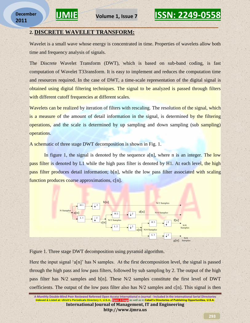
A schematic of three stage DWT decomposition is shown in Fig. 1.
In figure 1, the signal is denoted by the sequence a[n], where n is an integer. The low
pass filter is denoted by L1 while the high pass filter is denoted by H1. At each level, the high
pass filter produces detail information; b[n], while the low pass filter associated with scaling
function produces coarse approximations, c[n].
Figure 1. Three stage DWT decomposition using pyramid algorithm.
Here the input signal „a[n]‟ has N samples. At the first decomposition level, the signal is passed
through the high pass and low pass filters, followed by sub sampling by 2. The output of the high
pass filter has N/2 samples and b[n]. These N/2 samples constitute the first level of DWT
coefficients. The output of the low pass filter also has N/2 samples and c[n]. This signal is then

IJMIE Volume 1, Issue 7 ISSN: 2249-0558 __________________________________________________________
A Monthly Double-Blind Peer Reviewed Refereed Open Access International e-Journal - Included in the International Serial Directories Indexed & Listed at: Ulrich's Periodicals Directory ©, U.S.A., Open J-Gage as well as in Cabell’s Directories of Publishing Opportunities, U.S.A.
International Journal of Management, IT and Engineering http://www.ijmra.us
294
December 2011
passed through the same low pass and high pass filters for further decomposition. The output of
the second low pass filter followed by sub sampling has N/4 samples and e[n]. The output of the
second high pass filter followed by sub sampling has N/4 samples and d[n]. The second high
pass filtered
Signal constitutes the second level of DWT coefficients. The low pass filter output is then
filtered once again for further decomposition and produces g[n], f[n] with N/8 samples. The
filtering and decimation process is continued until the desired level is reached. The maximum
number of levels depends on the length of the signal. The DWT of the original signal is then
obtained by concatenating all the coefficients, starting from the last level of decomposition.
2.2 DATA DEPENDANCIES WITHIN DWT:
The wavelet decomposition of a 1-D input signal for three stages is shown in Fig. 1. The transfer
functions of the sixth order high pass (g (n)) and low pass (h (n)) FIR filter can be expressed as
follows:
High (z) = g0 + g1z-1
+ g2z-2
+ g3z-3
+ g4z-4
+ g5z-5
(1a)
Low (z) = h0 + h1z-1
+ h2z-2
+ h3z-3
+ h4z-4
+ h5z-5
(1b)
For clarity, the intermediate and final DWT coefficients in Fig. 1, are denoted by a, b, c, d, e, f
and g. The DWT computation is complex because of the data dependencies at different octaves.
Eq. 3a-3n shows the relationship among a, b, c, d, e, f and g. We note that the data dependencies
at various octaves are represented by identical symbols used in more than one octave equation.
1st octave:
b(0) = g(0)a(0) + g(1)a(-1) + g(2)a(-2) + g(3)a(-3) + g(4)a(-4) + g(5)a(-5)……(3a)
b(2) = g(0)a(2) + g(1)a(1) + g(2)a(0) + g(3)a(-1) + g(4)a(-2) + g(5)a(-3)……...(3b)
b(4) = g(0)a(4) + g(1)a(3) + g(2)a(2) + g(3)a(1) + g(4)a(0) + g(5)a(-1)………..(3c)
b(6) = g(0)a(6) + g(1)a(5) + g(2)a(4) + g(3)a(3) + g(4)a(2) + g(5)a(1) ……….(3d)
c(0) = h(0)a(0) + h(1)a(-1) + h(2)a(-2) + h(3)a(-3) + h(4)a(-4) + h(5)a(-5) …...(3e)
c(2) = h(0)a(2) + h(1)a(1) + h(2)a(0) + h(3)a(-1) + h(4)a(-2) + h(5)a(-3) ……..(3f)
IJMIE Volume 1, Issue 7 ISSN: 2249-0558 __________________________________________________________
A Monthly Double-Blind Peer Reviewed Refereed Open Access International e-Journal - Included in the International Serial Directories Indexed & Listed at: Ulrich's Periodicals Directory ©, U.S.A., Open J-Gage as well as in Cabell’s Directories of Publishing Opportunities, U.S.A.
International Journal of Management, IT and Engineering http://www.ijmra.us
295
December 2011
c(4) = h(0)a(4) + h(1)a(3) + h(2)a(2) + h(3)a(1) + h(4)a(0) + h(5)a(-1) ……….(3g)
c(6) = h(0)a(6) + h(1)a(5) + h(2)a(4) + h(3)a(3) + h(4)a(2) + h(5)a(1) ………..(3h)
2nd octave:
d(0) = g(0)c(0) + g(1)c(-2) + g(2)c(-4) + g(3)c(-6) + g(4)c(-8) + g(5)c(-10) …..(3i)
d(4) = g(0)c(4) + g(1)c(2) + g(2)c(0) + g(3)c(-2) + g(4)c(-4) + g(5)c(-6) ……...(3j)
e(0) = h(0)c(0) + h(1)c(-2) + h(2)c(-4) + h(3)c(-6) + h(4)c(-8) + h(5)c(-10) …..(3k)
e(4)= h(0)c(4) + h(1)c(2) + h(2)c(0) + h(3)c(-2) + h(4)c(-4) + h(5)c(-6) ……...(3l)
3rd octave:
f(0) = g(0)e(0) + g(1)e(-4) + g(2)e(-8) + g(3)e(-12) + g(4)e(-16) + g(5)e(-20)….(3m)
g(0) = h(0)e(0) + h(1)e(-4) + h(2)e(-8) + h(3)e(-12) + h(4)e(-16) + h(5)e(-20) ….(3n)
3. THE PROPOSED SYSTOLIC ARRAY ARCHITETURE:
The proposed systolic array (DWT-SA) architecture is an improved architecture. Here, only one
set of multipliers and adders has been employed. The multiplier and adder set performs all
necessary computations to generate all high pass and low pass coefficients. In addition, since a
set of registers controlled by a global clock is employed, the control circuitry does not need to
take the intermediate products in and out of the memory. This results in a simple and efficient
systolic implementation for 1-D DWT computation.
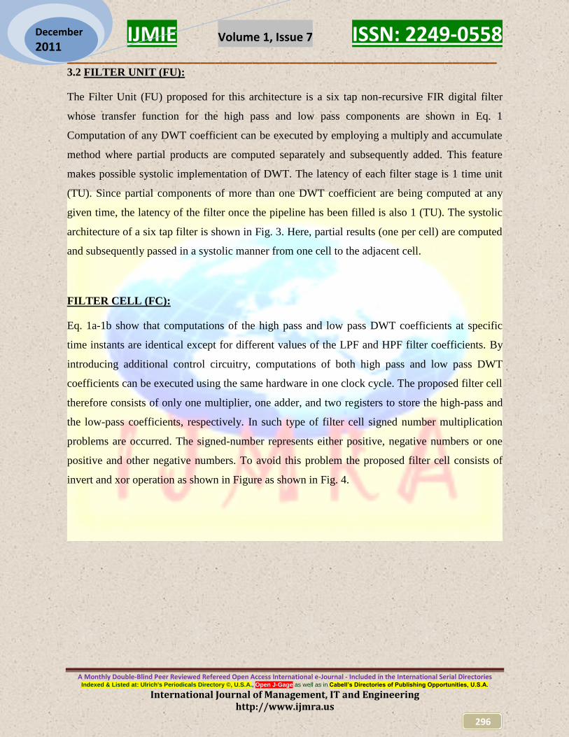
3.1 DWT-SA ARCHITECTURE:
The design of DWT-SA is based on a computation schedule derived from Eq. 3a - 3n which are
the result of applying the pyramid algorithm for eight data points (N = 8) to the six tap filter. We
note that Eq. 1a and 1b represent the high pass and low pass components of the six tap FIR filter.
The proposed DWT-SA architecture is shown in Fig. 2. It comprises of four basic units: Input
Delay, Filter, Register Bank, and Control unit.
IJMIE Volume 1, Issue 7 ISSN: 2249-0558 __________________________________________________________
A Monthly Double-Blind Peer Reviewed Refereed Open Access International e-Journal - Included in the International Serial Directories Indexed & Listed at: Ulrich's Periodicals Directory ©, U.S.A., Open J-Gage as well as in Cabell’s Directories of Publishing Opportunities, U.S.A.
International Journal of Management, IT and Engineering http://www.ijmra.us
296
December 2011
3.2 FILTER UNIT (FU):
The Filter Unit (FU) proposed for this architecture is a six tap non-recursive FIR digital filter
whose transfer function for the high pass and low pass components are shown in Eq. 1
Computation of any DWT coefficient can be executed by employing a multiply and accumulate
method where partial products are computed separately and subsequently added. This feature
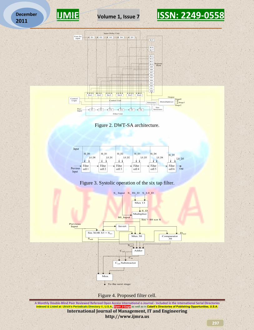
makes possible systolic implementation of DWT. The latency of each filter stage is 1 time unit
(TU). Since partial components of more than one DWT coefficient are being computed at any
given time, the latency of the filter once the pipeline has been filled is also 1 (TU). The systolic
architecture of a six tap filter is shown in Fig. 3. Here, partial results (one per cell) are computed
and subsequently passed in a systolic manner from one cell to the adjacent cell.
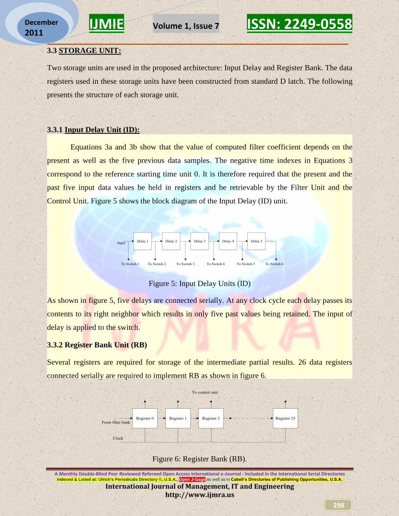
FILTER CELL (FC):
Eq. 1a-1b show that computations of the high pass and low pass DWT coefficients at specific
time instants are identical except for different values of the LPF and HPF filter coefficients. By
introducing additional control circuitry, computations of both high pass and low pass DWT
coefficients can be executed using the same hardware in one clock cycle. The proposed filter cell
therefore consists of only one multiplier, one adder, and two registers to store the high-pass and
the low-pass coefficients, respectively. In such type of filter cell signed number multiplication
problems are occurred. The signed-number represents either positive, negative numbers or one
positive and other negative numbers. To avoid this problem the proposed filter cell consists of
invert and xor operation as shown in Figure as shown in Fig. 4.
IJMIE Volume 1, Issue 7 ISSN: 2249-0558 __________________________________________________________
A Monthly Double-Blind Peer Reviewed Refereed Open Access International e-Journal - Included in the International Serial Directories Indexed & Listed at: Ulrich's Periodicals Directory ©, U.S.A., Open J-Gage as well as in Cabell’s Directories of Publishing Opportunities, U.S.A.
International Journal of Management, IT and Engineering http://www.ijmra.us
297
December 2011
Figure 2. DWT-SA architecture.
Figure 3. Systolic operation of the six tap filter.
Figure 4. Proposed filter cell.
IJMIE Volume 1, Issue 7 ISSN: 2249-0558 __________________________________________________________
A Monthly Double-Blind Peer Reviewed Refereed Open Access International e-Journal - Included in the International Serial Directories Indexed & Listed at: Ulrich's Periodicals Directory ©, U.S.A., Open J-Gage as well as in Cabell’s Directories of Publishing Opportunities, U.S.A.
International Journal of Management, IT and Engineering http://www.ijmra.us
298
December 2011
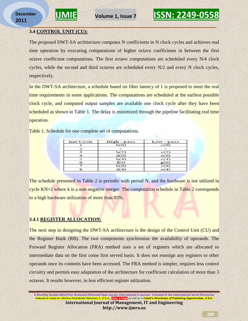
3.3 STORAGE UNIT:
Two storage units are used in the proposed architecture: Input Delay and Register Bank. The data
registers used in these storage units have been constructed from standard D latch. The following
presents the structure of each storage unit.
3.3.1 Input Delay Unit (ID):
Equations 3a and 3b show that the value of computed filter coefficient depends on the
present as well as the five previous data samples. The negative time indexes in Equations 3
correspond to the reference starting time unit 0. It is therefore required that the present and the
past five input data values be held in registers and be retrievable by the Filter Unit and the
Control Unit. Figure 5 shows the block diagram of the Input Delay (ID) unit.
Figure 5: Input Delay Units (ID)
As shown in figure 5, five delays are connected serially. At any clock cycle each delay passes its
contents to its right neighbor which results in only five past values being retained. The input of
delay is applied to the switch.
3.3.2 Register Bank Unit (RB)
Several registers are required for storage of the intermediate partial results. 26 data registers
connected serially are required to implement RB as shown in figure 6.
Figure 6: Register Bank (RB).
IJMIE Volume 1, Issue 7 ISSN: 2249-0558 __________________________________________________________
A Monthly Double-Blind Peer Reviewed Refereed Open Access International e-Journal - Included in the International Serial Directories Indexed & Listed at: Ulrich's Periodicals Directory ©, U.S.A., Open J-Gage as well as in Cabell’s Directories of Publishing Opportunities, U.S.A.
International Journal of Management, IT and Engineering http://www.ijmra.us
299
December 2011
3.4 CONTROL UNIT (CU):
The proposed DWT-SA architecture computes N coefficients in N clock cycles and achieves real
time operation by executing computations of higher octave coefficients in between the first
octave coefficient computations. The first octave computations are scheduled every N/4 clock
cycles, while the second and third octaves are scheduled every N/2 and every N clock cycles,
respectively.
In the DWT-SA architecture, a schedule based on filter latency of 1 is proposed to meet the real
time requirements in some applications. The computations are scheduled at the earliest possible
clock cycle, and computed output samples are available one clock cycle after they have been
scheduled as shown in Table 1. The delay is minimized through the pipeline facilitating real time
operation.
Table 1. Schedule for one complete set of computations.
The schedule presented in Table 2 is periodic with period N, and the hardware is not utilized in
cycle KN+2 where k is a non-negative integer. The computation schedule in Table 2 corresponds
to a high hardware utilization of more than 85%.
3.4.1 REGISTER ALLOCATION:
The next step in designing the DWT-SA architecture is the design of the Control Unit (CU) and
the Register Bank (RB). The two components synchronize the availability of operands. The
Forward Register Allocation (FRA) method uses a set of registers which are allocated to
intermediate data on the first come first served basis. It does not reassign any registers to other
operands once its contents have been accessed. The FRA method is simpler, requires less control
circuitry and permits easy adaptation of the architecture for coefficient calculation of more than 3
octaves. It results however, in less efficient register utilization.
IJMIE Volume 1, Issue 7 ISSN: 2249-0558 __________________________________________________________
A Monthly Double-Blind Peer Reviewed Refereed Open Access International e-Journal - Included in the International Serial Directories Indexed & Listed at: Ulrich's Periodicals Directory ©, U.S.A., Open J-Gage as well as in Cabell’s Directories of Publishing Opportunities, U.S.A.
International Journal of Management, IT and Engineering http://www.ijmra.us
300
December 2011
FRA Register Allocation:
In the FRA register allocation approach where data moves systolically in one direction only, it is
possible to increase the number of DWT decomposition octaves by placing additional registers in
series after register R26. The new registers hold the intermediate coefficients needed for the
computation of the next octave decomposition. Hardware utilization of the higher octave
decomposition registers is inversely proportional to the order of computed coefficients.
3.4.2 ACTIVITY PERIODS:
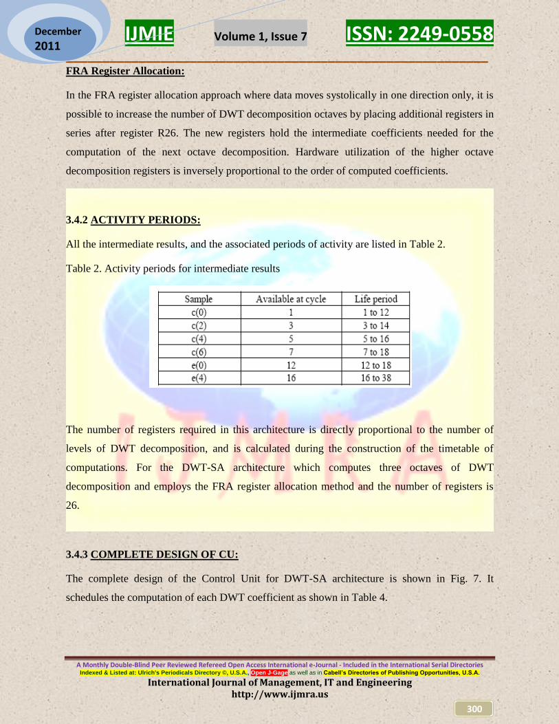
All the intermediate results, and the associated periods of activity are listed in Table 2.
Table 2. Activity periods for intermediate results
The number of registers required in this architecture is directly proportional to the number of
levels of DWT decomposition, and is calculated during the construction of the timetable of
computations. For the DWT-SA architecture which computes three octaves of DWT
decomposition and employs the FRA register allocation method and the number of registers is
26.
3.4.3 COMPLETE DESIGN OF CU:
The complete design of the Control Unit for DWT-SA architecture is shown in Fig. 7. It
schedules the computation of each DWT coefficient as shown in Table 4.
IJMIE Volume 1, Issue 7 ISSN: 2249-0558 __________________________________________________________
A Monthly Double-Blind Peer Reviewed Refereed Open Access International e-Journal - Included in the International Serial Directories Indexed & Listed at: Ulrich's Periodicals Directory ©, U.S.A., Open J-Gage as well as in Cabell’s Directories of Publishing Opportunities, U.S.A.
International Journal of Management, IT and Engineering http://www.ijmra.us
301
December 2011
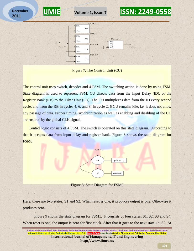
Figure 7. The Control Unit (CU)
The control unit uses switch, decoder and 4 FSM. The switching action is done by using FSM.
State diagram is used to represent FSM. CU directs data from the Input Delay (ID), or the
Register Bank (RB) to the Filter Unit (FU). The CU multiplexes data from the ID every second
cycle, and from the RB in cycles 4, 6, and 8. In cycle 2, 6 CU remains idle, i.e. it does not allow
any passage of data. Proper timing, synchronization as well as enabling and disabling of the CU
are ensured by the global CLK signal.
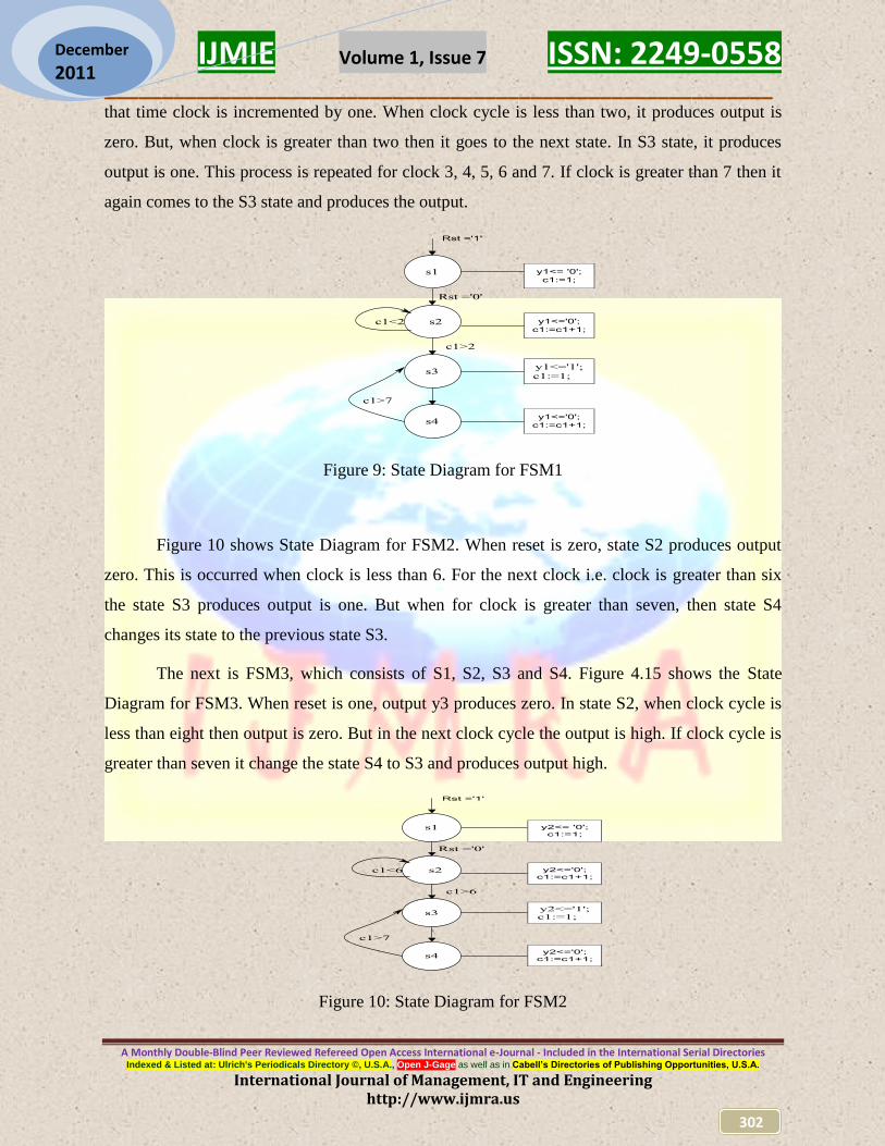
Control logic consists of 4 FSM. The switch is operated on this state diagram. According to
that it accepts data from input delay and register bank. Figure 8 shows the state diagram for
FSM0.
Figure 8: State Diagram for FSM0
Here, there are two states, S1 and S2. When reset is one, it produces output is one. Otherwise it
produces zero.
Figure 9 shows the state diagram for FSM1. It consists of four states, S1, S2, S3 and S4.
When reset is one, the output is zero for first clock. After that it goes to the next state i.e. S2. At
IJMIE Volume 1, Issue 7 ISSN: 2249-0558 __________________________________________________________
A Monthly Double-Blind Peer Reviewed Refereed Open Access International e-Journal - Included in the International Serial Directories Indexed & Listed at: Ulrich's Periodicals Directory ©, U.S.A., Open J-Gage as well as in Cabell’s Directories of Publishing Opportunities, U.S.A.
International Journal of Management, IT and Engineering http://www.ijmra.us
302
December 2011
that time clock is incremented by one. When clock cycle is less than two, it produces output is
zero. But, when clock is greater than two then it goes to the next state. In S3 state, it produces
output is one. This process is repeated for clock 3, 4, 5, 6 and 7. If clock is greater than 7 then it
again comes to the S3 state and produces the output.
Figure 9: State Diagram for FSM1
Figure 10 shows State Diagram for FSM2. When reset is zero, state S2 produces output
zero. This is occurred when clock is less than 6. For the next clock i.e. clock is greater than six
the state S3 produces output is one. But when for clock is greater than seven, then state S4
changes its state to the previous state S3.
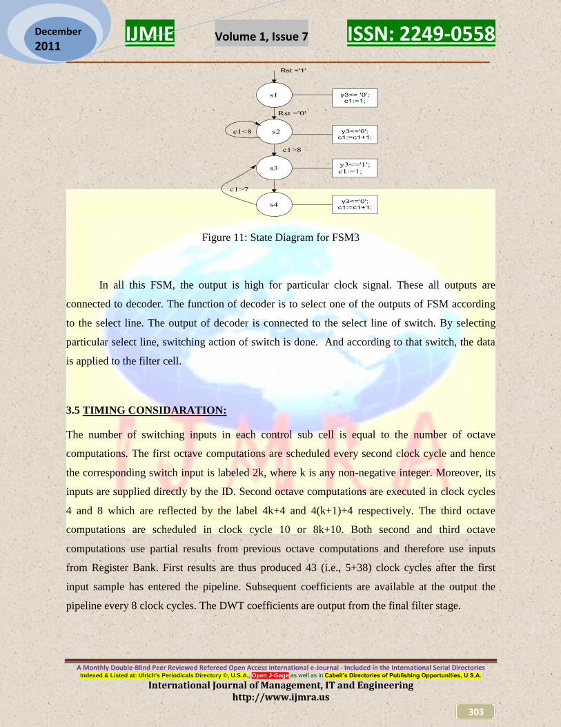
The next is FSM3, which consists of S1, S2, S3 and S4. Figure 4.15 shows the State
Diagram for FSM3. When reset is one, output y3 produces zero. In state S2, when clock cycle is
less than eight then output is zero. But in the next clock cycle the output is high. If clock cycle is
greater than seven it change the state S4 to S3 and produces output high.
Figure 10: State Diagram for FSM2
IJMIE Volume 1, Issue 7 ISSN: 2249-0558 __________________________________________________________
A Monthly Double-Blind Peer Reviewed Refereed Open Access International e-Journal - Included in the International Serial Directories Indexed & Listed at: Ulrich's Periodicals Directory ©, U.S.A., Open J-Gage as well as in Cabell’s Directories of Publishing Opportunities, U.S.A.
International Journal of Management, IT and Engineering http://www.ijmra.us
303
December 2011
Figure 11: State Diagram for FSM3
In all this FSM, the output is high for particular clock signal. These all outputs are
connected to decoder. The function of decoder is to select one of the outputs of FSM according
to the select line. The output of decoder is connected to the select line of switch. By selecting
particular select line, switching action of switch is done. And according to that switch, the data
is applied to the filter cell.
3.5 TIMING CONSIDARATION:
The number of switching inputs in each control sub cell is equal to the number of octave
computations. The first octave computations are scheduled every second clock cycle and hence
the corresponding switch input is labeled 2k, where k is any non-negative integer. Moreover, its
inputs are supplied directly by the ID. Second octave computations are executed in clock cycles
4 and 8 which are reflected by the label 4k+4 and 4(k+1)+4 respectively. The third octave
computations are scheduled in clock cycle 10 or 8k+10. Both second and third octave
computations use partial results from previous octave computations and therefore use inputs
from Register Bank. First results are thus produced 43 (i.e., 5+38) clock cycles after the first
input sample has entered the pipeline. Subsequent coefficients are available at the output the
pipeline every 8 clock cycles. The DWT coefficients are output from the final filter stage.
IJMIE Volume 1, Issue 7 ISSN: 2249-0558 __________________________________________________________
A Monthly Double-Blind Peer Reviewed Refereed Open Access International e-Journal - Included in the International Serial Directories Indexed & Listed at: Ulrich's Periodicals Directory ©, U.S.A., Open J-Gage as well as in Cabell’s Directories of Publishing Opportunities, U.S.A.
International Journal of Management, IT and Engineering http://www.ijmra.us
304
December 2011
3.6 SIMULATION RASULT:
The proposed DWT-SA architecture has been fully simulated in order to validate its
functionality.
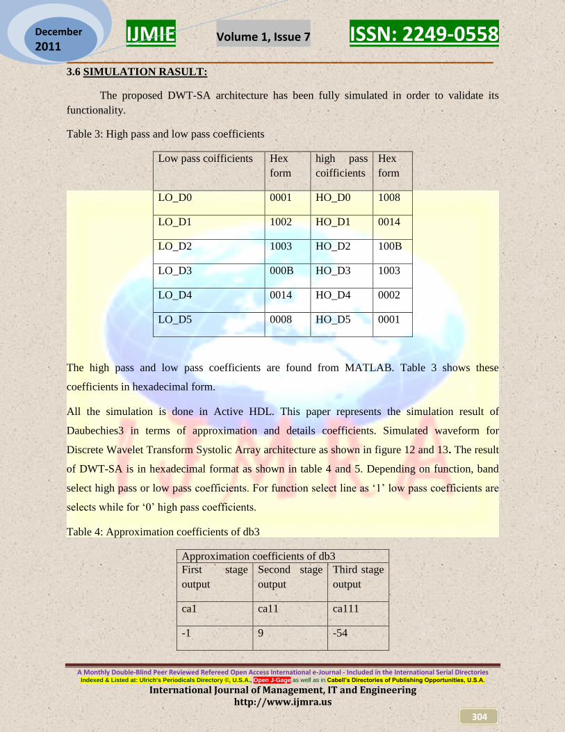
Table 3: High pass and low pass coefficients
Low pass coifficients Hex
form
high pass
coifficients
Hex
form
LO_D0 0001 HO_D0 1008
LO_D1 1002 HO_D1 0014
LO_D2 1003 HO_D2 100B
LO_D3 000B HO_D3 1003
LO_D4 0014 HO_D4 0002
LO_D5 0008 HO_D5 0001
The high pass and low pass coefficients are found from MATLAB. Table 3 shows these
coefficients in hexadecimal form.
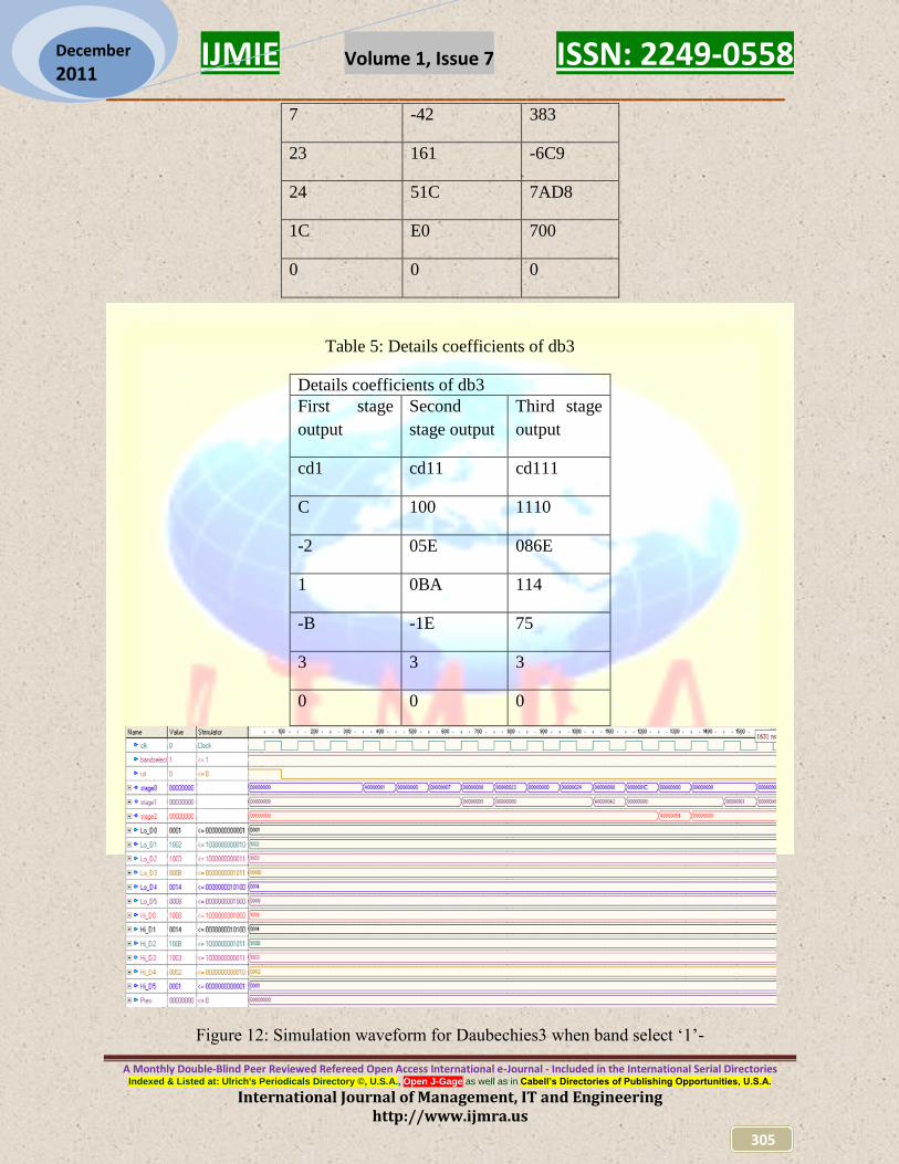
All the simulation is done in Active HDL. This paper represents the simulation result of
Daubechies3 in terms of approximation and details coefficients. Simulated waveform for
Discrete Wavelet Transform Systolic Array architecture as shown in figure 12 and 13. The result
of DWT-SA is in hexadecimal format as shown in table 4 and 5. Depending on function, band
select high pass or low pass coefficients. For function select line as „1‟ low pass coefficients are
selects while for „0‟ high pass coefficients.
Table 4: Approximation coefficients of db3
Approximation coefficients of db3
First stage
output
Second stage
output
Third stage
output
ca1 ca11 ca111
-1 9 -54
IJMIE Volume 1, Issue 7 ISSN: 2249-0558 __________________________________________________________
A Monthly Double-Blind Peer Reviewed Refereed Open Access International e-Journal - Included in the International Serial Directories Indexed & Listed at: Ulrich's Periodicals Directory ©, U.S.A., Open J-Gage as well as in Cabell’s Directories of Publishing Opportunities, U.S.A.
International Journal of Management, IT and Engineering http://www.ijmra.us
305
December 2011
7 -42 383
23 161 -6C9
24 51C 7AD8
1C E0 700
0 0 0
Table 5: Details coefficients of db3
Details coefficients of db3
First stage
output
Second
stage output
Third stage
output
cd1 cd11 cd111
C 100 1110
-2 05E 086E
1 0BA 114
-B -1E 75
3 3 3
0 0 0
Figure 12: Simulation waveform for Daubechies3 when band select „1‟-
IJMIE Volume 1, Issue 7 ISSN: 2249-0558 __________________________________________________________
A Monthly Double-Blind Peer Reviewed Refereed Open Access International e-Journal - Included in the International Serial Directories Indexed & Listed at: Ulrich's Periodicals Directory ©, U.S.A., Open J-Gage as well as in Cabell’s Directories of Publishing Opportunities, U.S.A.
International Journal of Management, IT and Engineering http://www.ijmra.us
306
December 2011
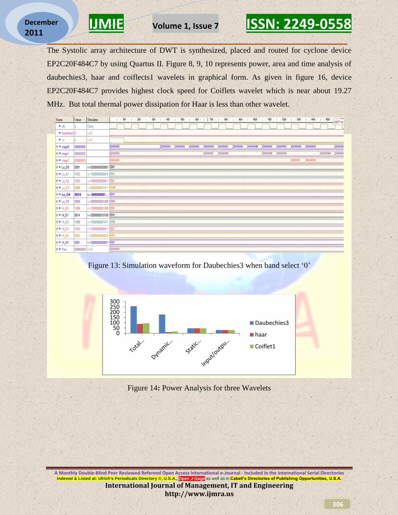
The Systolic array architecture of DWT is synthesized, placed and routed for cyclone device
EP2C20F484C7 by using Quartus II. Figure 8, 9, 10 represents power, area and time analysis of
daubechies3, haar and coiflects1 wavelets in graphical form. As given in figure 16, device
EP2C20F484C7 provides highest clock speed for Coiflets wavelet which is near about 19.27
MHz. But total thermal power dissipation for Haar is less than other wavelet.
Figure 13: Simulation waveform for Daubechies3 when band select „0‟
Figure 14: Power Analysis for three Wavelets
050
100150200250300
Daubechies3
haar
Coiflet1

IJMIE Volume 1, Issue 7 ISSN: 2249-0558 __________________________________________________________
A Monthly Double-Blind Peer Reviewed Refereed Open Access International e-Journal - Included in the International Serial Directories Indexed & Listed at: Ulrich's Periodicals Directory ©, U.S.A., Open J-Gage as well as in Cabell’s Directories of Publishing Opportunities, U.S.A.
International Journal of Management, IT and Engineering http://www.ijmra.us
307
December 2011
Figure 15: Area Analysis for three Wavelets
`
Figure 16: Time Analysis for three Wavelets
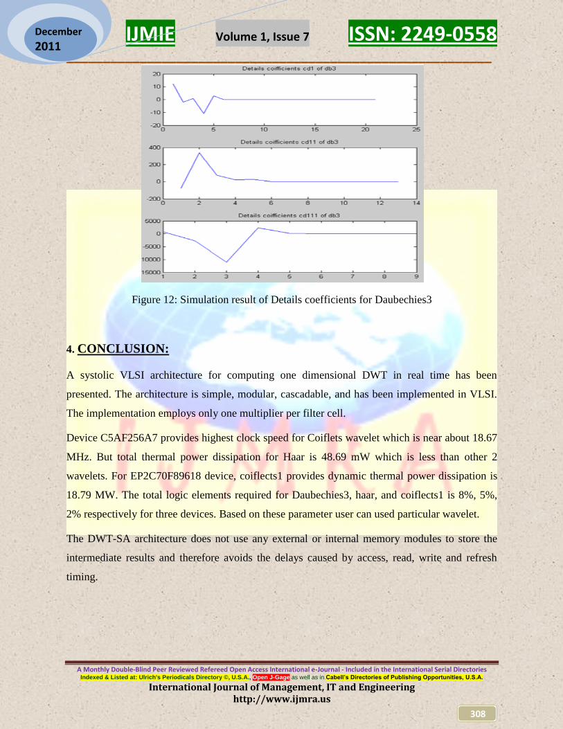
For the verification of VLSI result, MATLAB is used. The approximation and details
coefficients are obtained from MATLAB. Figure shows the simulation waveform for
approximation and details coefficients for three stages.
Figure 17: Simulation result of Approximation coefficients for Daubechies3
010002000300040005000
Coiflet1
haar
Daubechies3
0204060
Clock Period
Clock Speed
IJMIE Volume 1, Issue 7 ISSN: 2249-0558 __________________________________________________________
A Monthly Double-Blind Peer Reviewed Refereed Open Access International e-Journal - Included in the International Serial Directories Indexed & Listed at: Ulrich's Periodicals Directory ©, U.S.A., Open J-Gage as well as in Cabell’s Directories of Publishing Opportunities, U.S.A.
International Journal of Management, IT and Engineering http://www.ijmra.us
308
December 2011
Figure 12: Simulation result of Details coefficients for Daubechies3
4. CONCLUSION:
A systolic VLSI architecture for computing one dimensional DWT in real time has been
presented. The architecture is simple, modular, cascadable, and has been implemented in VLSI.
The implementation employs only one multiplier per filter cell.
Device C5AF256A7 provides highest clock speed for Coiflets wavelet which is near about 18.67
MHz. But total thermal power dissipation for Haar is 48.69 mW which is less than other 2
wavelets. For EP2C70F89618 device, coiflects1 provides dynamic thermal power dissipation is
18.79 MW. The total logic elements required for Daubechies3, haar, and coiflects1 is 8%, 5%,
2% respectively for three devices. Based on these parameter user can used particular wavelet.
The DWT-SA architecture does not use any external or internal memory modules to store the
intermediate results and therefore avoids the delays caused by access, read, write and refresh
timing.
IJMIE Volume 1, Issue 7 ISSN: 2249-0558 __________________________________________________________
A Monthly Double-Blind Peer Reviewed Refereed Open Access International e-Journal - Included in the International Serial Directories Indexed & Listed at: Ulrich's Periodicals Directory ©, U.S.A., Open J-Gage as well as in Cabell’s Directories of Publishing Opportunities, U.S.A.
International Journal of Management, IT and Engineering http://www.ijmra.us
309
December 2011
5. REFERENCES:
I. Daubechies, “Orthonormal bases of compactly supported wavelets,” Comm. Pure Appl.
Math, Vol. 41, pp. 906-966, 1988
S. G. Mallat, “A theory of multiresolution signal decomposition: the wavelet representation,”
IEEE Trans. on Pattern Recognition and Machine Intelligence, Vol. 11, No. 7, July 1989.
M. Vetterli and C. Harley, “Wavelets and filter banks: theory and design,” IEEE
Transactions on Signal processing, Vol. 40, No. 9, pp. 2207-2232, 1992.
R. A. Gopinath, Wavelets and Filter Banks – New Results and Applications, PhD
Dissertation, Rice University, Houston, Texas, 1993.
Y. Meyer, Wavelets: Algorithms and Applications, SIAM, Philadelphia, 1993.
A. N. Akansu and R. A. Haddad, Multiresolution Signal Decomposition: Transform, Sub
bands and Wavelets, Academic Press Inc., 1992.
O. Rioul and M. Vetterli, “Wavelets and signal processing,” IEEE Signal processing
Magazine, pp. 14-38, Oct. 1991.
R. A. Devore, B. Jawerth and B. J. Lacier, “Image compression through wavelet coding,”
IEEE Trans. on Information Theory, Vol. 38 .