interpolating dual-channel digital-to · pdf file dac5687 slws164e–february...
TRANSCRIPT

1FEATURES DESCRIPTION
APPLICATIONS
DAC5687
SLWS164E–FEBRUARY 2005–REVISED SEPTEMBER 2006www.ti.com
16-BIT, 500 MSPS 2×–8× INTERPOLATING DUAL-CHANNELDIGITAL-TO-ANALOG CONVERTER (DAC)
2345• 500 MSPS The DAC5687 is a dual-channel 16-bit high-speeddigital-to-analog converter (DAC) with integrated 2×,• Selectable 2×–8× Interpolation4×, and 8× interpolation filters, a complex numerically• On-Chip PLL/VCO Clock Multipliercontrolled oscillator (NCO), onboard clock multiplier,• Full IQ Compensation Including Offset, Gain,IQ compensation, and on-chip voltage reference. Theand PhaseDAC5687 is pin-compatible to the DAC5686,• Flexible Input Options: requiring only changes in register settings for most
– FIFO With Latch on External or Internal applications, and offers additional features andClock superior linearity, noise, crosstalk, and PLL phase
noise performance.– Even/Odd Multiplexed InputThe DAC5687 has six signal processing blocks: two– Single Port Demultiplexed Inputinterpolate-by-two digital filters, a fine frequency• Complex Mixer With 32-Bit NCOmixer with 32-bit NCO, a quadrature modulation
• Fixed Frequency Mixer With fS/4 and fS/2 compensation block, another interpolate-by-two digital• 1.8-V or 3.3-V I/O Voltage filter, and a coarse frequency mixer with fS/2 or fS/4.
The different modes of operation enable or bypass• On-Chip 1.2-V Referencethe signal processing blocks.• Differential Scalable Output: 2 mA to 20 mAThe coarse and fine mixers can be combined to span• Pin Compatible to DAC5686a wider range of frequencies with fine resolution. The
• High Performance DAC5687 allows both complex or real output.– 81-dBc ACLR WCDMA TM1 at 30.72 MHz Combining the frequency upconversion and complex
output produces a Hilbert transform pair that is output– 72-dBc ACLR WCDMA TM1 at 153.6 MHzfrom the two DACs. An external RF quadrature• Package: 100-Pin HTQFP modulator then performs the final single-sidebandupconversion.
The IQ compensation feature allows optimization of• Cellular Base Transceiver Station Transmit phase, gain, and offset to maximize sidebandChannel rejection and minimize LO feedthrough for an analog– CDMA: W-CDMA, CDMA2000, TD-SCDMA quadrature modulator.– TDMA: GSM, IS-136, EDGE/UWC-136
The DAC5687 includes several input options:– OFDM: 802.16 single-port interleaved data, even and odd• Cable Modem Termination System multiplexing at half-rate, and an input FIFO with either
external or internal clock to ease the input timingambiguity when the DAC5687 is clocked at the DACoutput sample rate.
ORDERING INFORMATIONTA Package Device
100 HTQFP (1) (PZP) PowerPAD™package, plastic quad flatpack–40°C to 85°C
DAC5687IPZP
(1) Thermal pad size: 6 mm × 6 mm.1
Please be aware that an important notice concerning availability, standard warranty, and use in critical applications ofTexas Instruments semiconductor products and disclaimers thereto appears at the end of this data sheet.
2PowerPAD is a trademark of Texas Instruments.3Excel is a trademark of Microsoft Corporation.4Matlab is a trademark of The MathWorks, Inc.5All other trademarks are the property of their respective owners.
PRODUCTION DATA information is current as of publication date. Copyright © 2005–2006, Texas Instruments IncorporatedProducts conform to specifications per the terms of the TexasInstruments standard warranty. Production processing does notnecessarily include testing of all parameters.

www.ti.com
22
CLK1
CLK1C
LPF
PLLLOCK
CLKVDD CLKGND DVDD DGNDPLLVDDPLLGND SLEEP
FIR1
sin
IOVDD
IOGND
AVDD AGND
PHSTR
NCO
cosRESETB
100-Pin HTQFP
EXTIO
EXTLO1.2-V
Reference
BIASJ
IOUTA1
IOUTA216-Bit
FIR4
IOUTB1
IOUTB2
FIR2
xsin(x)
TXENABLE
DA[15:0]
DB[15:0]
CLK2
CLK2C
SIF
SCLKSDENBSDOSDIO
DAC
16-BitDAC
2–8 fDATAInternal Clock Generation
and2–8 PLL Clock Multiplier
xsin(x)
A Gain
B Gain
AOffset
BOffset
B0019-02
QFLAG
Inpu
t FIF
O/
Reo
rder
/M
ux/D
emux
Fin
e M
ixer
Qua
drat
ure
Mod
Cor
rect
ion
(QM
C)
22
2
FIR3
Cou
rse
Mix
er:
fs/2
or
fs/4
2
DAC5687
SLWS164E–FEBRUARY 2005–REVISED SEPTEMBER 2006
These devices have limited built-in ESD protection. The leads should be shorted together or the device placed in conductive foamduring storage or handling to prevent electrostatic damage to the MOS gates.
FUNCTIONAL BLOCK DIAGRAM
2 Submit Documentation Feedback Copyright © 2005–2006, Texas Instruments Incorporated
Product Folder Link(s): DAC5687

www.ti.com
PINOUT
1
2
3
4
5
6
7
8
9
10
11
12
13
14
15
16
17
18
19
20
75
74
73
72
71
70
69
68
67
66
65
64
63
62
61
60
59
58
57
56
100 99 98 97 96 95 94 93 92 91 90 89 88 87 86 85 84 83 82
26 27 28 29 30 31 32 33 34 35 36 37 38 39 40
21
22
23
24
25
41 42 43 44 45 46 47 48 49 50
55
54
53
52
51
81 79 78 77 76
DAC5687
DV
DD
DG
ND
QF
LAG
TE
ST
MO
DE
SLE
EP
RE
SE
TB
PH
ST
R
DG
ND
DB
15 (
MS
B o
r LS
B)
DB
14
DB
13
DV
DD
DG
ND
DB
12
DB
11
DB
10
DB
9
DB
8
DV
DD
DG
ND
IOV
DD
IOG
ND
DB
7
DB
6
DB
5
DV
DD
DG
ND
SD
EN
B
SC
LK
SD
IO
SD
O
TX
EN
AB
LE
DA
15 (
MS
B o
r LS
B)
DA
14
DA
13
DV
DD
DG
ND
DA
12
DA
11
DA
10
DA
9
DA
8
DV
DD
DG
ND
IOV
DD
IOG
ND
DA
7
DA
6
DA
5
AVDD
AVDD
AVDD
AGND
IOUTA1
IOUTA2
AGND
AVDD
AGND
AVDD
EXTLO
AGND
BIASJ
AGND
EXTIO
AVDD
AGND
AVDD
AGND
IOUTB2
IOUTB1
AGND
AVDD
AVDD
AGND 80
DA4
DA3
DA2
DA1
DA0 (LSB or MSB)
DVDD
DGND
CLKGND
CLK1
CLK1C
CLKVDD
CLK2
CLK2C
CLKGND
PLLGND
LPF
PLLVDD
DVDD
DGND
PLLLOCK
DB0 (LSB or MSB)
DB1
DB2
DB3
DB4D
VD
D
P0011-02
PZP PACKAGE(TOP VIEW)
DAC5687
SLWS164E–FEBRUARY 2005–REVISED SEPTEMBER 2006
Copyright © 2005–2006, Texas Instruments Incorporated Submit Documentation Feedback 3
Product Folder Link(s): DAC5687
www.ti.com
DAC5687
SLWS164E–FEBRUARY 2005–REVISED SEPTEMBER 2006
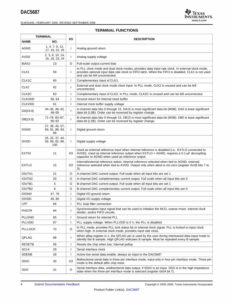
TERMINAL FUNCTIONSTERMINAL
I/O DESCRIPTIONNAME NO.
1, 4, 7, 9, 12,AGND I Analog ground return17, 19, 22, 252, 3, 8, 10, 14,AVDD I Analog supply voltage16, 18, 23, 24
BIASJ 13 O Full-scale output current biasIn PLL clock mode and dual clock modes, provides data input rate clock. In external clock mode,
CLK1 59 I provides optional input data rate clock to FIFO latch. When the FIFO is disabled, CLK1 is not usedand can be left unconnected.
CLK1C 60 I Complementary input of CLK1.External and dual clock mode clock input. In PLL mode, CLK2 is unused and can be leftCLK2 62 I unconnected.
CLK2C 63 I Complementary input of CLK2. In PLL mode, CLK2C is unused and can be left unconnected.CLKGND 58, 64 I Ground return for internal clock bufferCLKVDD 61 I Internal clock buffer supply voltage
34–36, 39–43, A-channel data bits 0 through 15. DA15 is most significant data bit (MSB). DA0 is least significantDA[15:0] I48–55 data bit (LSB). Order can be reversed by register change.71–78, 83–87, B-channel data bits 0 through 15. DB15 is most significant data bit (MSB). DB0 is least significantDB[15:0] I90–92 data bit (LSB). Order can be reversed by register change.27, 38, 45, 57,
DGND 69, 81, 88, 93, I Digital ground return99
26, 32, 37, 44,DVDD 56, 68, 82, 89, I Digital supply voltage
100Used as external reference input when internal reference is disabled (i.e., EXTLO connected to
EXTIO 11 I/O AVDD). Used as internal reference output when EXTLO = AGND, requires a 0.1-µF decouplingcapacitor to AGND when used as reference outputInternal/external reference select. Internal reference selected when tied to AGND, external
EXTLO 15 I/O reference selected when tied to AVDD. Output only when atest is not zero (register 0x1B bits 7 to3).
IOUTA1 21 O A-channel DAC current output. Full scale when all input bits are set 1IOUTA2 20 O A-channel DAC complementary current output. Full scale when all input bits are 0IOUTB1 5 O B-channel DAC current output. Full scale when all input bits are set 1IOUTB2 6 O B-channel DAC complementary current output. Full scale when all input bits are 0IOGND 47, 79 I Digital I/O ground returnIOVDD 46, 80 I Digital I/O supply voltageLPF 66 I PLL loop filter connection
Synchronization input signal that can be used to initialize the NCO, coarse mixer, internal clockPHSTR 94 I divider, and/or FIFO circuits.PLLGND 65 I Ground return for internal PLLPLLVDD 67 I PLL supply voltage. When PLLVDD is 0 V, the PLL is disabled.
In PLL mode, provides PLL lock status bit or internal clock signal. PLL is locked to input clockPLLLOCK 70 O when high. In external clock mode, provides input rate clock.When qflag register is 1, the QFLAG pin is used by the user during interleaved data input mode toQFLAG 98 I identify the B sample. High QFLAG indicates B sample. Must be repeated every B sample.
RESETB 95 I Resets the chip when low. Internal pullupSCLK 29 I Serial interface clockSDENB 28 I Active-low serial data enable, always an input to the DAC5687
Bidirectional serial data in three-pin interface mode, input-only in four-pin interface mode. Three-pinSDIO 30 I/O mode is the default after chip reset.Serial interface data, unidirectional data output, if SDIO is an input. SDO is in the high-impedanceSDO 31 O state when the three-pin interface mode is selected (register 0x04 bit 7).
4 Submit Documentation Feedback Copyright © 2005–2006, Texas Instruments Incorporated
Product Folder Link(s): DAC5687

www.ti.com
ABSOLUTE MAXIMUM RATINGS
THERMAL CHARACTERISTICS (1)
DAC5687
SLWS164E–FEBRUARY 2005–REVISED SEPTEMBER 2006
TERMINAL FUNCTIONS (continued)TERMINAL
I/O DESCRIPTIONNAME NO.SLEEP 96 I Asynchronous hardware power-down input. Active-High. Internal pulldown.
TXENABLE has two purposes. In all modes, TXENABLE must be high for the DATA to the DAC tobe enabled. When TXENABLE is low, the digital logic section is forced to all 0, and any input datapresented to DA[15:0] and DB[15:0] is ignored. In interleaved data mode, when the qflag registerTXENABLE 33 I bit is cleared, TXENABLE is used to synchronizes the data to channels A and B. The first dataafter the rising edge of TXENABLE is treated as A data, while the next data is treated as B data,and so on.
TESTMODE 97 I TESTMODE is DGND for the user
over operating free-air temperature range (unless otherwise noted) (1)
UNITAVDD (2) –0.5 V to 4 VDVDD (3) –0.5 V to 2.3 V
Supply voltage range CLKVDD (2) –0.5 V to 4 VIOVDD (2) –0.5 V to 4 VPLLVDD (2) –0.5 V to 4 V
Voltage between AGND, DGND, CLKGND, PLLGND, and IOGND –0.5 V to 0.5 VAVDD to DVDD –0.5 V to 2.6 VDA[15:0] (4) –0.5 V to IOVDD + 0.5 VDB[15:0] (4) –0.5 V to IOVDD + 0.5 VSLEEP (4) –0.5 V to IOVDD + 0.5 VCLK1/2, CLK1/2C (3) –0.5 V to CLKVDD + 0.5 V
Supply voltage rangeRESETB (4) –0.5 V to IOVDD + 0.5 VLPF (4) –0.5 V to PLLVDD + 0.5 VIOUT1, IOUT2 (2) –1 V to AVDD + 0.5 VEXTIO, BIASJ (2) –0.5 V to AVDD + 0.5 VEXTLO (2) –0.5 V to IAVDD + 0.5 V
Peak input current (any input) 20 mAPeak total input current (all inputs) 30 mA
TA Operating free-air temperature range (DAC5687I) –40°C to 85°CTstg Storage temperature range –65°C to 150°C
Lead temperature 1,6 mm (1/16 inch) from the case for 10 seconds 260°C
(1) Stresses beyond those listed under absolute maximum ratings may cause permanent damage to the device. These are stress ratingsonly, and functional operation of these or any other conditions beyond those indicated under recommended operating conditions is notimplied. Exposure to absolute-maximum-rated conditions for extended periods may affect device reliability.
(2) Measured with respect to AGND.(3) Measured with respect to DGND.(4) Measured with respect to IOGND.
over operating free-air temperature range (unless otherwise noted)
Thermal Conductivity 100 HTQFP UNITTJ Junction temperature (2) 105 °C
Theta junction-to-ambient (still air) 19.88 °C/WθJA Theta junction-to-ambient (150 lfm) (0.762 m/s) 14.37 °C/W
(1) Air flow or heat sinking reduces θJA and is highly recommended.(2) Air flow or heat sinking required for sustained operation at 85°C and maximum operating conditions to maintain junction temperature.
Copyright © 2005–2006, Texas Instruments Incorporated Submit Documentation Feedback 5
Product Folder Link(s): DAC5687

www.ti.com
ELECTRICAL CHARACTERISTICS (DC SPECIFICATIONS)
DAC5687
SLWS164E–FEBRUARY 2005–REVISED SEPTEMBER 2006
THERMAL CHARACTERISTICS (continued)over operating free-air temperature range (unless otherwise noted)
Thermal Conductivity 100 HTQFP UNITθJC Theta junction-to-case 0.12 °C/W
over recommended operating free-air temperature range, AVDD = 3.3 V, CLKVDD = 3.3 V, PLLVDD = 3.3 V, IOVDD = 3.3 V,DVDD = 1.8 V, IOUTFS = 19.2 mA (unless otherwise noted)
PARAMETER TEST CONDITIONS MIN TYP MAX UNITRESOLUTION 16 BitsDC ACCURACY (1)
1 LSB = IOUTFS/216INL Integral nonlinearity ±4 LSBTMIN to TMAX
DNL Differential nonlinearity ±4 LSBANALOG OUTPUT
Coarse gain linearity ±0.04 LSBWorst-case error from ideal linearity
Fine gain linearity ±3 LSBOffset error Mid code offset 0.01 %FSR
Without internal reference 1 %FSRGain error
With internal reference 0.7 %FSRWith internal reference, dual DAC, and SSBGain mismatch –2 2 %FSRmode
Minimum full-scale output current (2) 2 mAMaximum full-scale output current (2) 20 mA
AVDD – AVDDOutput compliance range (3) IOUTFS = 20 mA V0.5 V + 0.5 VOutput resistance 300 kΩOutput capacitance 5 pF
REFERENCE OUTPUTReference voltage 1.14 1.2 1.26 VReference output current (4) 100 nA
REFERENCE INPUTVEXTIO Input voltage range 0.1 1.25 V
Input resistance 1 MΩSmall signal bandwidth 1.4 MHzInput capacitance 100 pF
TEMPERATURE COEFFICIENTSppm ofOffset drift ±1 FSR/°C
Without internal reference ±15 ppm ofGain drift FSR/°CWith internal reference ±30ppm ofReference voltage drift ±8 FSR/°C
(1) Measured differential across IOUTA1 and IOUTA2 or IOUTB1 and IOUTB2 with 25 Ω each to AVDD.(2) Nominal full-scale current, IOUTFS , equals 32× the IBIAS current.(3) The upper limit of the output compliance is determined by the CMOS process. Exceeding this limit may result in transistor breakdown,
resulting in reduced reliability of the DAC5687 device. The lower limit of the output compliance is determined by the load resistors andfull-scale output current. Exceeding the limits adversely affects distortion performance and integral nonlinearity.
(4) Use an external buffer amplifier with high impedance input to drive any external load.
6 Submit Documentation Feedback Copyright © 2005–2006, Texas Instruments Incorporated
Product Folder Link(s): DAC5687

www.ti.com
DAC5687
SLWS164E–FEBRUARY 2005–REVISED SEPTEMBER 2006
ELECTRICAL CHARACTERISTICS (DC SPECIFICATIONS) (continued)over recommended operating free-air temperature range, AVDD = 3.3 V, CLKVDD = 3.3 V, PLLVDD = 3.3 V, IOVDD = 3.3 V,DVDD = 1.8 V, IOUTFS = 19.2 mA (unless otherwise noted)
PARAMETER TEST CONDITIONS MIN TYP MAX UNITPOWER SUPPLYAVDD Analog supply voltage 3 3.3 3.6 VDVDD Digital supply voltage 1.71 1.8 2.15 VCLKVDD Clock supply voltage 3 3.3 3.6 VIOVDD I/O supply voltage 1.71 3.6 VPLLVDD PLL supply voltage 3 3.3 3.6 V
Mode 5 (5) 41IAVDD Analog supply current mA
Mode 6 (5) 80IDVDD Digital supply current (5) Mode 6 (5) 587 mAICLKVDD Clock supply current (5) Mode 6 (5) 5 mAIPLLVDD PLL supply current (5) Mode 6 (5) 20 mAIIOVDD IO supply current (5) Mode 6 (5) 2 mA
Sleep mode (SLEEP pin high), CLK2 = 500IAVDD Sleep mode AVDD supply current 1 mAMHzSleep mode (SLEEP pin high), CLK2 = 500IDVDD Sleep mode DVDD supply current 2 mAMHz
Sleep mode CLKVDD supply Sleep mode (SLEEP pin high), CLK2 = 500ICLKVDD 0.25 mAcurrent MHzSleep mode (SLEEP pin high), CLK2 = 500IPLLVDD Sleep mode PLLVDD supply current 0.6 mAMHzSleep mode (SLEEP pin high), CLK2 = 500IIOVDD Sleep mode IOVDD supply current 0.6 mAMHzMode 1 (5) AVDD = 3.3 V, DVDD = 1.8 V 750Mode 2 (5) AVDD = 3.3 V, DVDD = 1.8 V 910Mode 3 (5) AVDD = 3.3 V, DVDD = 1.8 V 760Mode 4 (5) AVDD = 3.3 V, DVDD = 1.8 V 1250
PD Power dissipation mWMode 5 (5) AVDD = 3.3 V, DVDD = 1.8 V 1250Mode 6 (5) AVDD = 3.3 V, DVDD = 1.8 V 1410Mode 7 (5) AVDD = 3.3 V, DVDD = 1.8 V 1400 1750Sleep mode (SLEEP pin high), CLK2 = 500 11 20MHz
APSRR –0.2 0.2 %FSR/VPower supply rejection ratio
DPSRR –0.2 0.2 %FSR/V
(5) MODE 1 – MODE 7:a. Mode 1: X2, PLL off, CLK2 = 320 MHz, DACA and DACB on, IF = 5 MHzb. Mode 2: X4 QMC, PLL on, CLK1 = 125 MHz, DACA and DACB on, IF = 5 MHzc. Mode 3: X4 CMIX, PLL off, CLK2 = 500 MHz, DACA off and DACB on, IF = 150 MHzd. Mode 4: X4L FMIX CMIX, PLL off, CLK2 = 500 MHz, DACA off and DACB on, IF = 150 MHze. Mode 5: X4L FMIX CMIX, PLL on, CLK1 = 125 MHz, DACA off and DACB on, IF = 150 MHzf. Mode 6: X4L FMIX CMIX, PLL on, CLK1 = 125 MHz, DACA on and DACB on, IF = 150 MHzg. Mode 7: X8 FMIX CMIX, PLL on, CLK1 = 62.5 MHz, DACA and DACB on, IF = 150 MHz
Copyright © 2005–2006, Texas Instruments Incorporated Submit Documentation Feedback 7
Product Folder Link(s): DAC5687

www.ti.com
ELECTRICAL CHARACTERISTICS (AC SPECIFICATIONS) (1)
DAC5687
SLWS164E–FEBRUARY 2005–REVISED SEPTEMBER 2006
over recommended operating free-air temperature range, AVDD = 3.3 V, CLKVDD = 3.3 V, PLLVDD = 0 V (= 3.3 V for PLLclock mode), IOVDD = 3.3 V, DVDD = 1.8 V, IOUTFS = 19.2 mA, external clock mode, 4:1 transformer output termination,50-Ω doubly terminated load (unless otherwise noted)
PARAMETER TEST CONDITIONS MIN TYP MAX UNITANALOG OUTPUTfCLK Maximum output update rate 500 MSPSts(DAC) Output settling time to 0.1% Transition: Code 0x0000 to 0xFFFF 10.4 nstpd Output propagation delay 3 nstr(IOUT) Output rise time 10% to 90% 2 nstf(IOUT) Output fall time 90% to 10% 2 nsAC PERFORMANCE
X2, PLL off, CLK2 = 250 MHz, DAC A and DAC B on, 78IF = 5.1 MHz, first Nyquist zone < fDATA/2X4, PLL off, CLK2 = 500 MHz, DAC A and DAC B on, 77SFDR Spurious free dynamic range (2) IF = 5.1 MHz, first Nyquist zone < fDATA/2 dBcX4, CLK2 = 500 MHz, DAC A and DAC B on,IF = 20.1 MHz, PLL on for MIN, PLL off for TYP, 68 (3) 76first Nyquist zone < fDATA/2X4, PLL off, CLK2 = 500 MSPS, DAC A and DAC B on, 73single tone, 0 dBFS, IF = 20.1 MHzX4 CMIX, PLL off, CLK2 = 500 MSPS, DAC A and DAC B 65on, IF = 70.1 MHzX4 CMIX, PLL off, CLK2 = 500 MSPS, DAC A and DAC B 57SNR Signal-to-noise ratio on, single tone, 0 dBFS, IF = 150.1 MHz dBcX4 FMIX CMIX, PLL off, CLK2 = 500 MSPS, DAC A and 54DAC B on, single tone, 0 dBFS, IF = 180.1 MHzX4, PLL off, CLK2 = 500 MSPS, DAC A and DAC B on,four tones, each –12 dBFS, IF = 24.7, 24.9, 25.1, 25.3 73MHzX4, PLL off, CLK2 = 500 MSPS, DAC A and DAC B on, 79IF = 20.1 and 21.1 MHzX4 CMIX, PLL off, CLK2 = 500 MSPS, DAC A and DAC B 73Third-order two-tone on, IF = 70.1 and 71.1 MHz
IMD3 intermodulation (each tone at dBcX4 CMIX, PLL off, CLK2 = 500 MSPS, DAC A and DAC B–6 dBFS) 68on, IF= 150.1 and 151.1 MHzX4 FMIX CMIX, PLL off, CLK2 = 500 MSPS, DAC A and 67DAC B on, IF = 180.1 and 181.1 MHz
Four-tone intermodulation to X4 CMIX, CLK2 = 500 MHz, fOUT = 149.2, 149.6, 150.4,IMD Nyquist (each tone at –12 66 dBcand 150.8 MHzdBFS)
(1) Measured single ended into 50-Ω load.(2) See the Non-Harmonic Clock Related Spurious Signals section for information on spurious products out of band (< fDATA/2).(3) 1:1 transformer output termination.
8 Submit Documentation Feedback Copyright © 2005–2006, Texas Instruments Incorporated
Product Folder Link(s): DAC5687

www.ti.com
ELECTRICAL CHARACTERISTICS (DIGITAL SPECIFICATIONS)
DAC5687
SLWS164E–FEBRUARY 2005–REVISED SEPTEMBER 2006
ELECTRICAL CHARACTERISTICS (AC SPECIFICATIONS) (continued)over recommended operating free-air temperature range, AVDD = 3.3 V, CLKVDD = 3.3 V, PLLVDD = 0 V (= 3.3 V for PLLclock mode), IOVDD = 3.3 V, DVDD = 1.8 V, IOUTFS = 19.2 mA, external clock mode, 4:1 transformer output termination,50-Ω doubly terminated load (unless otherwise noted)
PARAMETER TEST CONDITIONS MIN TYP MAX UNITSingle carrier, baseband, X4, PLL clock mode, 78.4CLK1 = 122.88 MHzSingle carrier, baseband, X4, PLL clock mode, 78.5CLK2 = 491.52 MHzSingle carrier, IF = 153.6 MHz, X4 CMIX, external clock 70.9mode, CLK2 = 491.52 MHzTwo carrier, IF = 153.6 MHz, X4 CMIX, external clock 67.8mode, CLK2 = 491.52 MHzFour carrier, baseband, X4, external clock mode, 76.1CLK2 = 491.52 MHz
ACLR (4) Adjacent channel leakage ratio dBcFour carrier, IF = 92.16 MHz, X4L, external clock mode, 66.8CLK2 = 491.52 MHzSingle carrier, IF = 153.6 MHz, X4 CMIX, external clock 72.2mode, CLK2 = 491.52 MHz, DVDD = 2.1 VTwo carrier, IF = 153.6 MHz, X4 CMIX, external clock 69.3mode, CLK2 = 491.52 MHz, DVDD = 2.1 VFour carrier, baseband, X4, external clock mode, 68.5CLK2 = 491.52 MHz, DVDD = 2.1 VFour carrier, IF = 92.16 MHz, X4L, external clock mode, 66.3CLK2 = 491.52 MHz, DVDD = 2.1 V50-MHz offset, 1-MHz BW, single carrier, baseband, 92X4, external clock mode, CLK2 = 491.52 MHz50-MHz offset, 1-MHz BW, four carrier, baseband, 81X4, external clock mode, CLK2 = 491.52 MHz
Noise floor dBc50-MHz offset, 1-MHz BW, single carrier, baseband, 88X4, PLL clock mode, CLK1 = 122.88 MHz50-MHz offset, 1-MHz BW, four carrier, baseband, 81X4, PLL clock mode, CLK1 = 122.88 MHz
(4) W-CDMA with 3.84-MHz BW, 5-MHz spacing, centered at IF. TESTMODEL 1, 10 ms
over recommended operating free-air temperature range, AVDD = 3.3 V, CLKVDD = 3.3 V, PLLVDD = 3.3 V, IOVDD = 3.3 V,DVDD = 1.8 V, IOUTFS = 19.2 mA (unless otherwise noted)
PARAMETER TEST CONDITIONS MIN TYP MAX UNIT
CMOS INTERFACE
VIH High-level input voltage 2 3 V
VIL Low-level input voltage 0 0 0.8 V
VIH High-level input voltage IOVDD = 1.8 V 1.26 V
VIL Low-level input voltage IOVDD = 1.8 V 0.54 V
IIH High-level input current –40 40 µA
IIL Low-level input current –40 40 µA
Input capacitance 5 pF
Iload = –100 µA IOVDD – 0.2VOH PLLLOCK, SDO, SDIO V
Iload = –8 mA 0.8 IOVDD
Iload = 100 µA 0.2VOL PLLLOCK, SDO, SDIO V
Iload = 8 mA 0.22 IOVDD
External or dual-clock modes 0 250Input data rate MSPS
PLL clock mode 2.5 160
Copyright © 2005–2006, Texas Instruments Incorporated Submit Documentation Feedback 9
Product Folder Link(s): DAC5687
www.ti.com
CLK2
10.5
2f-
DAC5687
SLWS164E–FEBRUARY 2005–REVISED SEPTEMBER 2006
ELECTRICAL CHARACTERISTICS (DIGITAL SPECIFICATIONS) (continued)over recommended operating free-air temperature range, AVDD = 3.3 V, CLKVDD = 3.3 V, PLLVDD = 3.3 V, IOVDD = 3.3 V,DVDD = 1.8 V, IOUTFS = 19.2 mA (unless otherwise noted)
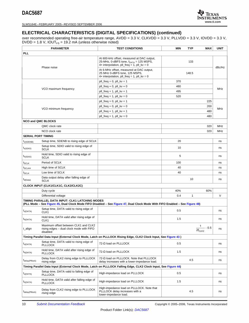
PARAMETER TEST CONDITIONS MIN TYP MAX UNIT
PLL
At 600-kHz offset, measured at DAC output,25-MHz, 0-dBFS tone, fDATA = 125 MSPS, 1334× interpolation, pll_freq = 1, pll_kv = 0
Phase noise dBc/HzAt 6-MHz offset, measured at DAC output,25 MHz 0-dBFS tone, 125 MSPS, 148.54× interpolation, pll_freq = 1, pll_kv = 0
pll_freq = 0, pll_kv = 1 370
pll_freq = 0, pll_kv = 0 480VCO maximum frequency MHz
pll_freq = 1, pll_kv = 1 495
pll_freq = 1, pll_kv = 0 520
pll_freq = 0, pll_kv = 1 225
pll_freq = 0, pll_kv = 0 200VCO minimum frequency MHz
pll_freq = 1, pll_kv = 1 480
pll_freq = 1, pll_kv = 0 480
NCO and QMC BLOCKS
QMC clock rate 320 MHz
NCO clock rate 320 MHz
SERIAL PORT TIMING
ts(SDENB) Setup time, SDENB to rising edge of SCLK 20 ns
Setup time, SDIO valid to rising edge ofts(SDIO) 10 nsSCLK
Hold time, SDIO valid to rising edge ofth(SDIO) 5 nsSCLK
tSCLK Period of SCLK 100 ns
tSCLKH High time of SCLK 40 ns
tSCLK Low time of SCLK 40 ns
Data output delay after falling edge oftd(Data) 10 nsSCLK
CLOCK INPUT (CLK1/CLK1C, CLK2/CLK2C)
Duty cycle 40% 60%
Differential voltage 0.4 1 V
TIMING PARALLEL DATA INPUT: CLK1 LATCHING MODES(PLL Mode – See Figure 45, Dual Clock Mode FIFO Disabled – See Figure 47, Dual Clock Mode With FIFO Enabled – See Figure 48)
Setup time, DATA valid to rising edge ofts(DATA) 0.5 nsCLK1
Hold time, DATA valid after rising edge ofth(DATA) 1.5 nsCLK1
Maximum offset between CLK1 and CLK2t_align rising edges – dual clock mode with FIFO ns
disabled
Timing Parallel Data Input (External Clock Mode, Latch on PLLLOCK Rising Edge, CLK2 Clock Input, See Figure 43 )
Setup time, DATA valid to rising edge ofts(DATA) 72-Ω load on PLLLOCK 0.5 nsPLLLOCK
Hold time, DATA valid after rising edge ofth(DATA) 72-Ω load on PLLLOCK 1.5 nsPLLLOCK
Delay from CLK2 rising edge to PLLLOCK 72-Ω load on PLLLOCK. Note that PLLLOCKtdelay(Plllock) 4.5 nsrising edge delay increases with a lower-impedance load.
Timing Parallel Data Input (External Clock Mode, Latch on PLLLOCK Falling Edge, CLK2 Clock Input, See Figure 44)
Setup time, DATA valid to falling edge ofts(DATA) High-impedance load on PLLLOCK 0.5 nsPLLLOCK
Hold time, DATA valid after falling edge ofth(DATA) High-impedance load on PLLLOCK 1.5 nsPLLLOCK
High-impedance load on PLLLOCK. Note thatDelay from CLK2 rising edge to PLLLOCKtdelay(Plllock) PLLLOCK delay increases with a 4.5 nsrising edge lower-impedance load.
10 Submit Documentation Feedback Copyright © 2005–2006, Texas Instruments Incorporated
Product Folder Link(s): DAC5687

www.ti.com
Typical Characteristics
Code
−8
−6
−4
−2
0
2
4
6
8
0 10000 20000 30000 40000 50000 60000 70000
Err
or −
LS
B
G001Code
−6
−4
−2
0
2
4
6
0 10000 20000 30000 40000 50000 60000 70000
Err
or −
LS
BG002
f − Frequency − MHz
−90
−80
−70
−60
−50
−40
−30
−20
−10
0
10
0 50 100 150 200 250
P −
Pow
er −
dB
m
G003
fdata = 125 MSPSfin = 20 MHz RealIF = 20 MHz4 InterpolationPLL Off
f − Frequency − MHz
−90
−80
−70
−60
−50
−40
−30
−20
−10
0
10
0 50 100 150 200 250
P −
Pow
er −
dB
m
G004
fdata = 125 MSPSfin = −30 MHz ComplexIF = 95 MHz4L InterpolationCMIXPLL Off
DAC5687
SLWS164E–FEBRUARY 2005–REVISED SEPTEMBER 2006
Figure 1. Integral Nonlinearity Figure 2. Differential Nonlinearity
Figure 3. Single-Tone Spectral Plot Figure 4. Single-Tone Spectral Plot
Copyright © 2005–2006, Texas Instruments Incorporated Submit Documentation Feedback 11
Product Folder Link(s): DAC5687

www.ti.com
f − Frequency − MHz
−90
−80
−70
−60
−50
−40
−30
−20
−10
0
10
0 50 100 150 200 250
fdata = 125 MSPSfin = 30 MHz RealIF = 155 MHz4L InterpolationHP/HPPLL Off
P −
Pow
er −
dB
m
G005IF − Intermediate Frequency − MHz
60
65
70
75
80
85
90
95
100
5 10 15 20 25 30 35
fdata = 125 MSPS4 InterpolationPLL Off
SF
DR
− S
purio
us-F
ree
Dyn
amic
Ran
ge −
dB
cG006
0 dBFS
−6 dBFS
−12 dBFS
IF − Intermediate Frequency − MHz
40
45
50
55
60
65
70
75
80
85
90
0 50 100 150 200 250
fdata = 125 MSPS4 InterpolationPLL Off
SF
DR
− S
purio
us-F
ree
Dyn
amic
Ran
ge −
dB
c
G007
0 dBFS
IF − Intermediate Frequency − MHz
50
55
60
65
70
75
80
85
90
95
100
0 50 100 150 200 250
fdata = 125 MSPS4L InterpolationPLL Offfout = IF 0.5 MHz
IMD
3 −
dBc
G008
0 dBFS
DAC5687
SLWS164E–FEBRUARY 2005–REVISED SEPTEMBER 2006
Typical Characteristics (continued)
Figure 5. Single-Tone Spectral Plot Figure 6. In-Band SFDR vs Intermediate Frequency
Figure 7. Out-of-Band SFDR vs Intermediate Frequency Figure 8. Two-Tone IMD vs Intermediate Frequency
12 Submit Documentation Feedback Copyright © 2005–2006, Texas Instruments Incorporated
Product Folder Link(s): DAC5687

www.ti.com
Amplitude − dBFS
40
45
50
55
60
65
70
75
80
85
90
−35 −30 −25 −20 −15 −10 −5 0
IMD
3 −
dBC
G009
fdata = 125 MSPSfin = −30 MHz 0.5 MHz ComplexIF = 95 MHz4L InterpolationCMIXPLL Off
f − Frequency − MHz
−100
−90
−80
−70
−60
−50
−40
−30
−20
−10
0
10 15 20 25 30
fdata = 125 MSPSf in = 20 MHz0.5 MHz RealIF = 20 MHz4 InterpolationPLL Off
P −
Pow
er −
dB
mG010
f − Frequency − MHz
−100
−90
−80
−70
−60
−50
−40
−30
−20
−10
0
85 90 95 100 105
fdata = 125 MSPSf in = −30 MHz0.5 MHz ComplexIF = 95 MHz4L InterpolationCMIXPLL Off
P −
Pow
er −
dB
m
G011IF − Intermediate Frequency − MHz
50
55
60
65
70
75
80
85
90
0 50 100 150 200 250
fdata = 122.88 MSPSBaseband InputDVDD = 1.8 V
AC
LR −
dB
c
G012
PLL On
PLL Off
DAC5687
SLWS164E–FEBRUARY 2005–REVISED SEPTEMBER 2006
Typical Characteristics (continued)
Figure 9. Two-Tone IMD vs Amplitude Figure 10. Two-Tone IMD Spectral Plot
Figure 11. Two-Tone IMD Spectral Plot Figure 12. WCDMA ACLR vs Intermediate Frequency
Copyright © 2005–2006, Texas Instruments Incorporated Submit Documentation Feedback 13
Product Folder Link(s): DAC5687

www.ti.com
f − Frequency − MHz
−130
−120
−110
−100
−90
−80
−70
−60
−50
−40
−30
−20
−10
18 23 28 33 38 43
P −
Pow
er −
dB
m
G013
Carrier Power: −7.99 dBmACLR (5 MHz): 81.24 dBACLR (10 MHz): 83.79 dBfdata = 122.88 MSPSIF = 30.72 MHz4 Interpolation
f − Frequency − MHz
−130
−120
−110
−100
−90
−80
−70
−60
−50
−40
−30
−20
−10
18 23 28 33 38 43
P −
Pow
er −
dB
mG014
Carrier Power: −7.99 dBmACLR (5 MHz): 75.8 dBACLR (10 MHz): 80.18 dBfdata = 122.88 MSPSIF = 30.72 MHz4 Interpolation
f − Frequency − MHz
−130
−120
−110
−100
−90
−80
−70
−60
−50
−40
−30
−20
−10
80 85 90 95 100 105
P −
Pow
er −
dB
m
G015
Carrier Power: −8.7 dBmACLR (5 MHz): 75.97 dBACLR (10 MHz): 77.47 dBfdata = 122.88 MSPSIF = 92.16 MHz4 InterpolationCMIX
f − Frequency − MHz
−130
−120
−110
−100
−90
−80
−70
−60
−50
−40
−30
−20
−10
80 85 90 95 100 105
P −
Pow
er −
dB
m
G016
Carrier Power: −8.7 dBmACLR (5 MHz): 67.43 dBACLR (10 MHz): 73.21 dBfdata = 122.88 MSPSIF = 92.16 MHz4 InterpolationCMIX
DAC5687
SLWS164E–FEBRUARY 2005–REVISED SEPTEMBER 2006
Typical Characteristics (continued)
Figure 13. WCDMA TM1: Single Carrier, PLL Off, Figure 14. WCDMA TM1: Single Carrier, PLL On,DVDD = 1.8 V DVDD = 1.8 V
Figure 15. WCDMA TM1: Single Carrier, PLL Off, Figure 16. WCDMA TM1: Single Carrier, PLL On,DVDD = 1.8 V DVDD = 1.8 V
14 Submit Documentation Feedback Copyright © 2005–2006, Texas Instruments Incorporated
Product Folder Link(s): DAC5687

www.ti.com
f − Frequency − MHz
−130
−120
−110
−100
−90
−80
−70
−60
−50
−40
−30
−20
−10
141 146 151 156 161 166
P −
Pow
er −
dB
m
G017
Carrier Power: −10.35 dBmACLR (5 MHz): 72.06 dBACLR (10 MHz): 73.21 dBfdata = 122.88 MSPSIF = 153.6 MHz4 InterpolationCMIX
f − Frequency − MHz
−130
−120
−110
−100
−90
−80
−70
−60
−50
−40
−30
−20
−10
141 146 151 156 161 166
P −
Pow
er −
dB
mG018
Carrier Power: −10.35 dBmACLR (5 MHz): 63.12 dBACLR (10 MHz): 69.17 dBfdata = 122.88 MSPSIF = 153.6 MHz4 InterpolationCMIX
f − Frequency − MHz
−130
−120
−110
−100
−90
−80
−70
−60
−50
−40
−30
−20
−10
138 143 148 153 158 163 168
P −
Pow
er −
dB
m
G019
Carrier Power 1 (Ref): −15.78 dBmACLR (5 MHz): 68.19 dBACLR (10 MHz): 69.48 dBfdata = 122.88 MSPSIF = 153.6 MHz4 InterpolationCMIX
f − Frequency − MHz
−130
−120
−110
−100
−90
−80
−70
−60
−50
−40
−30
−20
−10
138 143 148 153 158 163 168
P −
Pow
er −
dB
m
G020
Carrier Power 1 (Ref): −15.78 dBmACLR (5 MHz): 61.28 dBACLR (10 MHz): 64.61 dBfdata = 122.88 MSPSIF = 153.6 MHz4 InterpolationCMIX
DAC5687
SLWS164E–FEBRUARY 2005–REVISED SEPTEMBER 2006
Typical Characteristics (continued)
Figure 17. WCDMA TM1: Single Carrier, PLL Off, Figure 18. WCDMA TM1: Single Carrier, PLL On,DVDD = 1.8 V DVDD = 1.8 V
Figure 19. WCDMA TM1: Two Carriers, PLL Off, Figure 20. WCDMA TM1: Two Carriers, PLL On,DVDD = 1.8 V DVDD = 1.8 V
Copyright © 2005–2006, Texas Instruments Incorporated Submit Documentation Feedback 15
Product Folder Link(s): DAC5687

www.ti.com
f − Frequency − MHz
−130
−120
−110
−100
−90
−80
−70
−60
−50
−40
−30
−20
72 77 82 87 92 97 102 107 112
P −
Pow
er −
dB
m
G021
fdata = 122.88 MSPSIF = 92.16 MHz4 InterpolationCMIX
Carrier Power 1 (Ref): −17.41 dBmACLR (5 MHz): 69.09 dBACLR (10 MHz): 69.34 dB
f − Frequency − MHz
−130
−120
−110
−100
−90
−80
−70
−60
−50
−40
−30
−20
72 77 82 87 92 97 102 107 112
P −
Pow
er −
dB
mG022
fdata = 122.88 MSPSIF = 92.16 MHz4 InterpolationCMIX
Carrier Power 1 (Ref): −17.42 dBmACLR (5 MHz): 64 dBACLR (10 MHz): 65.79 dB
f − Frequency − MHz
−130
−120
−110
−100
−90
−80
−70
−60
−50
−40
−30
−20
−10
141 146 151 156 161 166
P −
Pow
er −
dB
m
G023
Carrier Power: −10.35 dBmACLR (5 MHz): 73.83 dBACLR (10 MHz): 75.39 dBfdata = 122.88 MSPSIF = 153.6 MHz4 InterpolationCMIX
f − Frequency − MHz
−130
−120
−110
−100
−90
−80
−70
−60
−50
−40
−30
−20
−10
138 143 148 153 158 163 168
P −
Pow
er −
dB
m
G024
Carrier Power 1 (Ref): −15.77 dBmACLR (5 MHz): 69.74 dBACLR (10 MHz): 71.17 dBfdata = 122.88 MSPSIF = 153.6 MHz4 InterpolationCMIX
DAC5687
SLWS164E–FEBRUARY 2005–REVISED SEPTEMBER 2006
Typical Characteristics (continued)
Figure 21. WCDMA TM1: Four Carriers, PLL Off, Figure 22. WCDMA TM1: Four Carriers, PLL On,DVDD = 1.8 V DVDD = 1.8 V
Figure 23. WCDMA TM1: Single Carrier, PLL Off, Figure 24. WCDMA TM1: Two Carriers, PLL Off,DVDD = 2.1 V DVDD = 2.1 V
16 Submit Documentation Feedback Copyright © 2005–2006, Texas Instruments Incorporated
Product Folder Link(s): DAC5687

www.ti.com
f − Frequency − MHz
−130
−120
−110
−100
−90
−80
−70
−60
−50
−40
−30
−20
133 138 143 148 153 158 163 168 173
P −
Pow
er −
dB
m
G025
fdata = 122.88 MSPSIF = 153.6 MHz4 InterpolationCMIX
Carrier Power 1 (Ref): −19.88 dBmACLR (5 MHz): 66.6 dBACLR (10 MHz): 65.73 dB
Test Methodology
DAC5687
SLWS164E–FEBRUARY 2005–REVISED SEPTEMBER 2006
Typical Characteristics (continued)
Figure 25. WCDMA TM1: Four Carriers, PLL Off,DVDD = 2.1 V
Typical ac specifications in external clock mode were characterized with the DAC5687EVM using the testconfiguration shown in Figure 26. The DAC sample-rate clock fDAC is generated by an HP8665B signalgenerator. An Agilent 8133A pulse generator is used to divide fDAC for the data-rate clock fDATA for the Agilent16702A pattern-generator clock and provide adjustable skew to the DAC input clock. The 8133A fDAC output isset to 1 VPP, equivalent to 2-VPP differential at CLK2/CLK2C pins. Alternatively, the DAC5687 PLLLOCK outputcan be used for the pattern generator clock.
The DAC5687 output is characterized with a Rohde & Schwarz FSQ8 spectrum analyzer. For WCDMA signalcharacterization, it is important to use a spectrum analyzer with high IP3 and noise subtraction capability so thatthe spectrum analyzer does not limit the ACPR measurement. For all specifications, both DACA and DACB aremeasured and the lowest value used as the specification.
Copyright © 2005–2006, Texas Instruments Incorporated Submit Documentation Feedback 17
Product Folder Link(s): DAC5687

www.ti.com
CLK2
CLK2C
LPF
PLLLOCK
DG
ND
PLL
VD
D
PLL
GN
D
SLE
EP
IOGND
IOVDD
AV
DD
AG
ND
PH
ST
R
RESETB
EXTIO
EXTLO
BIASJ
IOUTA1
IOUTA2
IOUTB1
IOUTB2TXENABLE
DA[15:0]
DB[15:0]
CEXTIO0.1 µF
RBIAS1 kΩ
3.3 V
3.3 V
100 Ω
HP8665BSynthesized
SignalGenerator
1:4
Mini CircuitsTCM4−1W
200 Ω
0.01 µF
16
Agilent 16702BMainframe System
With16720A PatternGenerator Card
Rohde & SchwarzFSQ8
SpectrumAnalyzer
PULSEFREQ. = fdata
93.1 Ω0.033 µF
330 pF
CLK
VD
D
CLK
GN
D
Agilent 8133APulse Generator
CLK1CLK1C
DV
DD
(Not
Incl
udin
g P
in 5
6)
1.8 V/2.1 V
10 Ω 10 pF
DV
DD
(Pin
56)
3.3 V
16
PULSEFREQ. = fDACAmpl. = 1 V PP
1:4
Mini CircuitsT4−1
3.3 V
3.3 V
100 Ω
3.3 V
SinusoidFREQ. = fDAC
B0039-01
3.3 V
DAC5687
SLWS164E–FEBRUARY 2005–REVISED SEPTEMBER 2006
Figure 26. DAC5687 Test Configuration for External Clock Mode
PLL clock mode was characterized using the test configuration shown in Figure 27. The DAC data rate clockfDATA is generated by an HP8665B signal generator. An Agilent 8133A pulse generator is used to generate aclock fDATA for the Agilent 16702A pattern-generator clock and provide adjustable skew to the DAC input clock.The 8133A fDAC output is set to 1 VPP, equivalent to 2-VPP differential at CLK1/CLK1C pins. Alternatively, theDAC5687 PLLLOCK output can be used for the pattern-generator clock.
18 Submit Documentation Feedback Copyright © 2005–2006, Texas Instruments Incorporated
Product Folder Link(s): DAC5687

www.ti.com
CLK1
CLK1C
LPF
PLLLOCK
DG
ND
PLL
VD
D
PLL
GN
D
SLE
EP
IOGND
IOVDD
AV
DD
AG
ND
PH
ST
R
RESETB
EXTIO
EXTLO
BIASJ
IOUTA1
IOUTA2
IOUTB1
IOUTB2TXENABLE
DA[15:0]
DB[15:0]
CEXTIO0.1 µF
RBIAS1 kΩ
3.3 V
3.3 V
100 Ω
HP8665BSynthesized
SignalGenerator
1:4
Mini CircuitsTCM4−1W
200 Ω
0.01 µF
16
Agilent 16702BMainframe System
With16720A PatternGenerator Card
Rohde & SchwarzFSQ8
SpectrumAnalyzer
PULSEFREQ. = fdata
93.1 Ω0.033 µF
330 pF
CLK
VD
D
CLK
GN
D
Agilent 8133APulse Generator
CLK2CLK2C
DV
DD
(Not
Incl
udin
g P
in 5
6)
1.8 V/2.1 V
10 Ω 10 pF
DV
DD
(Pin
56)
3.3 V
16
PULSEFREQ. = fdataAmpl. = 1 V PP
1:4
Mini CircuitsT4−1
3.3 V
3.3 V
100 Ω
3.3 V
SinusoidFREQ. = fdata
B0039-02
3.3 V
DAC5687
SLWS164E–FEBRUARY 2005–REVISED SEPTEMBER 2006
Figure 27. DAC5687 Test Configuration for PLL Clock Mode
WCDMA test-model-1 test vectors for the DAC5687 characterization were generated in accordance with the3GPP Technical Specification. Chip-rate data was generated using the test-model-1 block in the Agilent ADS.For multicarrier signals, different random seeds and PN offsets were used for each carrier. A Matlab™ scriptperformed pulse shaping, interpolation to the DAC input data rate, frequency offsets, rounding, and scaling. Eachtest vector is 10 ms long, representing one frame. Special care is taken to assure that the end of the file wrapssmoothly to the beginning of the file.
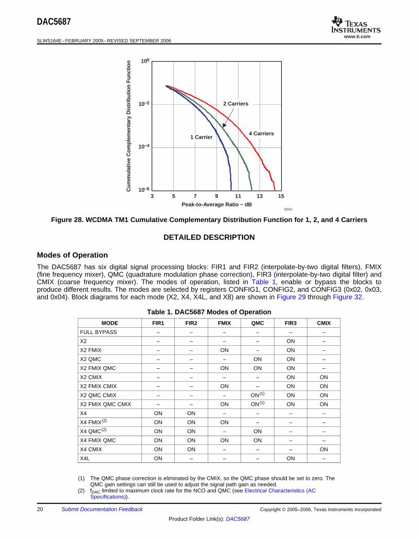
The cumulative complementary distribution function (CCDF) for the 1-, 2-, and 4-carrier test vectors is shown inFigure 28. The test vectors are scaled such that the absolute maximum data point is 0.95 (–0.45 dB) of full scale.No peak reduction is used.
Copyright © 2005–2006, Texas Instruments Incorporated Submit Documentation Feedback 19
Product Folder Link(s): DAC5687
www.ti.com
Peak-to-Average Ratio − dB
3 5 7 9 11 13 15
Cum
mul
ativ
e C
ompl
emen
tary
Dis
tribu
tion
Fun
ctio
n
G041
10−6
1 Carrier
2 Carriers
4 Carriers
10−4
10−2
100
DETAILED DESCRIPTION
Modes of Operation
DAC5687
SLWS164E–FEBRUARY 2005–REVISED SEPTEMBER 2006
Figure 28. WCDMA TM1 Cumulative Complementary Distribution Function for 1, 2, and 4 Carriers
The DAC5687 has six digital signal processing blocks: FIR1 and FIR2 (interpolate-by-two digital filters), FMIX(fine frequency mixer), QMC (quadrature modulation phase correction), FIR3 (interpolate-by-two digital filter) andCMIX (coarse frequency mixer). The modes of operation, listed in Table 1, enable or bypass the blocks toproduce different results. The modes are selected by registers CONFIG1, CONFIG2, and CONFIG3 (0x02, 0x03,and 0x04). Block diagrams for each mode (X2, X4, X4L, and X8) are shown in Figure 29 through Figure 32.
Table 1. DAC5687 Modes of OperationMODE FIR1 FIR2 FMIX QMC FIR3 CMIX
FULL BYPASS – – – – – –X2 – – – – ON –X2 FMIX – – ON – ON –X2 QMC – – – ON ON –X2 FMIX QMC – – ON ON ON –X2 CMIX – – – – ON ONX2 FMIX CMIX – – ON – ON ONX2 QMC CMIX – – – ON (1) ON ONX2 FMIX QMC CMIX – – ON ON (1) ON ONX4 ON ON – – – –X4 FMIX (2) ON ON ON – – –X4 QMC (2) ON ON – ON – –X4 FMIX QMC ON ON ON ON – –X4 CMIX ON ON – – – ONX4L ON – – – ON –
(1) The QMC phase correction is eliminated by the CMIX, so the QMC phase should be set to zero. TheQMC gain settings can still be used to adjust the signal path gain as needed.
(2) fDAC limited to maximum clock rate for the NCO and QMC (see Electrical Characteristics (ACSpecifications)).
20 Submit Documentation Feedback Copyright © 2005–2006, Texas Instruments Incorporated
Product Folder Link(s): DAC5687

www.ti.com
sin
NCO
cos
IOUTA1
IOUTA216-Bit
FIR4
IOUTB1
IOUTB2
xsin(x)
DA[15:0]
DB[15:0]
DAC
16-BitDAC
xsin(x)
A Gain
B Gain
AOffset
BOffset
B0160-01
Inpu
t For
mat
ter
Fin
e M
ixer
Qua
drat
ure
Mod
Cor
rect
ion
(QM
C)
2
FIR3
Cou
rse
Mix
er:
fs/2
or
fs/4
2
DAC5687
SLWS164E–FEBRUARY 2005–REVISED SEPTEMBER 2006
Table 1. DAC5687 Modes of Operation (continued)MODE FIR1 FIR2 FMIX QMC FIR3 CMIX
X4L FMIX ON – ON – ON –X4L QMC ON – – ON ON –X4L FMIX QMC ON – ON ON ON –X4L CMIX ON – – – ON ONX4L FMIX CMIX ON – ON ON ONX4L QMC CMIX ON – – ON (2) ON ONX4L FMIX QMC CMIX ON – ON ON (2) ON ONX8 ON ON – – ON –X8 FMIX ON ON ON – ON –X8 QMC ON ON – ON ON –X8 FMIX QMC ON ON ON ON ON –X8 CMIX ON ON – – ON ONX8 FMIX CMIX ON ON ON – ON ONX8 QMC CMIX ON ON – ON (1) ON ONX8 FMIX QMC CMIX ON ON ON ON (1) ON ON
Figure 29. Block Diagram for X2 Mode
Copyright © 2005–2006, Texas Instruments Incorporated Submit Documentation Feedback 21
Product Folder Link(s): DAC5687

www.ti.com
22
FIR1
sin
NCO
cos
IOUTA1
IOUTA216-Bit
FIR4
IOUTB1
IOUTB2
FIR2
xsin(x)
DA[15:0]
DB[15:0]
DAC
16-BitDAC
xsin(x)
A Gain
B Gain
AOffset
BOffset
B0161-01
Inpu
t For
mat
ter
Fin
e M
ixer
Qua
drat
ure
Mod
Cor
rect
ion
(QM
C)
22
FIR1 FIR2 Cou
rse
Mix
er:
fs/2
or
fs/4
2
FIR1
sin
NCO
cos
IOUTA1
IOUTA216-Bit
FIR4
IOUTB1
IOUTB2
xsin(x)
DA[15:0]
DB[15:0]
DAC
16-BitDAC
xsin(x)
A Gain
B Gain
AOffset
BOffset
B0162-01
Inpu
t For
mat
ter
Fin
e M
ixer
Qua
drat
ure
Mod
Cor
rect
ion
(QM
C)
2
2
FIR3
Cou
rse
Mix
er:
fs/2
or
fs/4
2
DAC5687
SLWS164E–FEBRUARY 2005–REVISED SEPTEMBER 2006
A. FMIX or QMC block cannot be enabled with CMIX block.
Figure 30. Block Diagram for X4 Mode (A)
Figure 31. Block Diagram for X4L Mode
22 Submit Documentation Feedback Copyright © 2005–2006, Texas Instruments Incorporated
Product Folder Link(s): DAC5687

www.ti.com
22
FIR1
sin
NCO
cos
IOUTA1
IOUTA216-Bit
FIR4
IOUTB1
IOUTB2
FIR2
xsin(x)
DA[15:0]
DB[15:0]
DAC
16-BitDAC
xsin(x)
A Gain
B Gain
AOffset
BOffset
B0163-01
Inpu
t For
mat
ter
Fin
e M
ixer
Qua
drat
ure
Mod
Cor
rect
ion
(QM
C)
22
2
FIR3
Cou
rse
Mix
er:
fs/2
or
fs/4
2
DAC5687
SLWS164E–FEBRUARY 2005–REVISED SEPTEMBER 2006
Figure 32. Block Diagram for X8 Mode
Copyright © 2005–2006, Texas Instruments Incorporated Submit Documentation Feedback 23
Product Folder Link(s): DAC5687
www.ti.com
Programming Registers
Register Name: VERSION—Address: 0x00, Default = 0x03
DAC5687
SLWS164E–FEBRUARY 2005–REVISED SEPTEMBER 2006
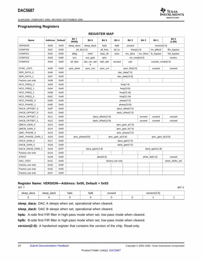
REGISTER MAPBit 7 Bit 0Name Address Default Bit 6 Bit 5 Bit 4 Bit 3 Bit 2 Bit 1(MSB) (LSB)
VERSION 0x00 0x03 sleep_daca sleep_dacb hpla hplb unused version(2:0)
CONFIG0 0x01 0x00 pll_div(1:0) pll_freq pll_kv interp(1:0) inv_plllock fifo_bypass
CONFIG1 0x02 0x00 qflag interl dual_clk twos rev_abus rev_bbus fir_bypass full_bypass
CONFIG2 0x03 0x80 nco nco_gain qmc cm_mode(3:0) invsinc
CONFIG3 0x04 0x00 sif_4pin dac_ser_dat half_rate unused usb counter_mode(2:0)a
SYNC_CNTL 0x05 0x00 sync_phstr sync_nco sync_cm sync_fifo(2:0) unused unused
SER_DATA_0 0x06 0x00 dac_data(7:0)
SER_DATA_1 0x07 0x00 dac_data(15:8)
Factory use only 0x08 0x00
NCO_FREQ_0 0x09 0x00 freq(7:0)
NCO_FREQ_1 0x0A 0x00 freq(15:8)
NCO_FREQ_2 0x0B 0x00 freq(23:16)
NCO_FREQ_3 0x0C 0x40 freq(31:24)
NCO_PHASE_0 0x0D 0x00 phase(7:0)
NCO_PHASE_1 0x0E 0x00 phase(15:8)
DACA_OFFSET_0 0x0F 0x00 daca_offset(7:0)
DACB_OFFSET_0 0x10 0x00 dacb_offset(7:0)
DACA_OFFSET_1 0x11 0x00 daca_offset(12:8) unused unused unused
DACB_OFFSET_1 0x12 0x00 dacb_offset(12:8) unused unused unused
QMCA_GAIN_0 0x13 0x00 qmc_gain_a(7:0)
QMCB_GAIN_0 0x14 0x00 qmc_gain_b(7:0)
QMC_PHASE_0 0x15 0x00 qmc_phase(7:0)
QMC_PHASE_GAIN_1 0x16 0x00 qmc_phase(9:8) qmc_gain_a(10:8) qmc_gain_b(10:8)
DACA_GAIN_0 0x17 0x00 daca_gain(7:0)
DACB_GAIN_0 0x18 0x00 dacb_gain(7:0)
DACA_DACB_GAIN_1 0x19 0xFF daca_gain(11:8) dacb_gain(11:8)
Factory use only 0x1A 0x00
ATEST 0x1B 0x00 atest(4:0) phstr_del(1:0) unused
DAC_TEST 0x1C 0x00 factory use only phstr_clkdiv_sel
Factory use only 0x1D 0x00
Factory use only 0x1E 0x00
Factory use only 0x1F 0x00
BIT 7 BIT 0
sleep_daca sleep_dacb hpla hplb unused version(2:0)0 0 0 0 0 0 1 1
sleep_daca: DAC A sleeps when set, operational when cleared.
sleep_dacb: DAC B sleeps when set, operational when cleared.
hpla: A-side first FIR filter in high-pass mode when set, low-pass mode when cleared.
hplb: B-side first FIR filter in high-pass mode when set, low-pass mode when cleared.
version(2:0): A hardwired register that contains the version of the chip. Read-only.
24 Submit Documentation Feedback Copyright © 2005–2006, Texas Instruments Incorporated
Product Folder Link(s): DAC5687

www.ti.com
Register Name: CONFIG0—Address: 0x01, Default = 0x00
Register Name: CONFIG1—Address: 0x02, Default = 0x00
DAC5687
SLWS164E–FEBRUARY 2005–REVISED SEPTEMBER 2006
BIT 7 BIT 0
pll_div(1:0) pll_freq pll_kv interp(1:0) inv_plllock fifo_bypass0 0 0 0 0 0 0 0
pll_div(1:0): PLL VCO divider; 00 = 1, 01 = 2, 10 = 4, 11 = 8.
pll_freq: PLL VCO center frequency; 0 = low center frequency, 1 = high center frequency.
pll_kv: PLL VCO gain; 0 = high gain, 1 = low gain.
interp(1:0): FIR interpolation; 00 = X2, 01 = X4, 10 = X4L, 11 = X8. X4 uses lower power than X4L, but fDAC =320 MHz maximum when NCO or QMC is used.
inv_plllock: Multifunction bit, depending on clock mode
fifo_bypass: When set, the internal four-sample FIFO is disabled. When cleared, the FIFO is enabled.
Table 2. inv_plllock Bit ModesPLLVDD dual_clk inv_plllock fifo_bypass DESCRIPTION
0 V 0 0 1 Input data latched on PLLLOCK pin rising edges, FIFO disabled0 V 0 1 1 Input data latched on PLLLOCK pin falling edges, FIFO disabled0 V 0 0 0 Input data latched on PLLLOCK pin rising edges, FIFO enabled
and must be synchronized0 V 0 1 0 Input data latched on PLLLOCK pin falling edges, FIFO enabled
and must be synchronized0 V 1 0 1 Input data latched on CLK1/CLK1C differential input. Timing
between CLK1 and CLK2 rising edges must be tightly controlled(500 ps maximum at 500-MHz CLK2). PLLLOCK output signal isalways low. The FIFO is always disabled in this mode.
0 V 1 1 0 Input data latched on CLK1/CLK1C differential input. No phaserelationship required between CLK1 and CLK2. The FIFO isemployed to manage the internal handoff between the CLK1input clock and the CLK2 derived output clock; the FIFO mustbe synchronized. The PLLLOCK output signal reflects theinternally generated FIFO output clock.
0 V 1 0 0 Not a valid setting. Do not use.0 V 1 1 1 Not a valid setting. Do not use.
3.3 V X X 1 Internal PLL enabled, CLK1/CLK1C input differential clock isused to latch the input data. The FIFO is always disabled in thismode.
3.3 V X X 0 Not a valid setting. Do not use.
BIT 7 BIT 0
qflag interl dual_clk twos rev_abus rev_bbus fir_bypass full_bypass0 0 0 0 0 0 0 0
qflag: When set, the QFLAG input pin operates as a B sample indicator when interleaved data is enabled. Whencleared, the TXENABLE rising determines the A/B timing relationship.
interl: When set, interleaved input data mode is enabled; both A and B data streams are input at the DA[15:0]input pins.
dual_clk: Only used when the PLL is disabled. When set, two differential clocks are used to input the data to thechip; CLK1/CLK1C is used to latch the input data into the chip and CLK2/CLK2C is used as the DACsample clock.
twos: When set, input data is interpreted as 2s complement. When cleared, input data is interpreted as offsetbinary.
rev_abus: When cleared, DA input data MSB to LSB order is DA[15] = MSB and DA[0] = LSB. When set, DA
Copyright © 2005–2006, Texas Instruments Incorporated Submit Documentation Feedback 25
Product Folder Link(s): DAC5687
www.ti.com
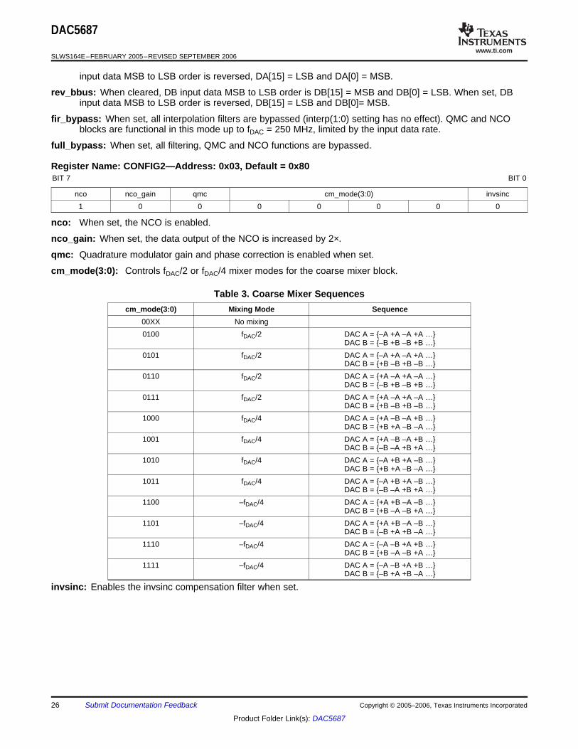
Register Name: CONFIG2—Address: 0x03, Default = 0x80
DAC5687
SLWS164E–FEBRUARY 2005–REVISED SEPTEMBER 2006
input data MSB to LSB order is reversed, DA[15] = LSB and DA[0] = MSB.
rev_bbus: When cleared, DB input data MSB to LSB order is DB[15] = MSB and DB[0] = LSB. When set, DBinput data MSB to LSB order is reversed, DB[15] = LSB and DB[0]= MSB.
fir_bypass: When set, all interpolation filters are bypassed (interp(1:0) setting has no effect). QMC and NCOblocks are functional in this mode up to fDAC = 250 MHz, limited by the input data rate.
full_bypass: When set, all filtering, QMC and NCO functions are bypassed.
BIT 7 BIT 0
nco nco_gain qmc cm_mode(3:0) invsinc1 0 0 0 0 0 0 0
nco: When set, the NCO is enabled.
nco_gain: When set, the data output of the NCO is increased by 2×.
qmc: Quadrature modulator gain and phase correction is enabled when set.
cm_mode(3:0): Controls fDAC/2 or fDAC/4 mixer modes for the coarse mixer block.
Table 3. Coarse Mixer Sequencescm_mode(3:0) Mixing Mode Sequence
00XX No mixing0100 fDAC/2 DAC A = –A +A –A +A …
DAC B = –B +B –B +B …0101 fDAC/2 DAC A = –A +A –A +A …
DAC B = +B –B +B –B …0110 fDAC/2 DAC A = +A –A +A –A …
DAC B = –B +B –B +B …0111 fDAC/2 DAC A = +A –A +A –A …
DAC B = +B –B +B –B …1000 fDAC/4 DAC A = +A –B –A +B …
DAC B = +B +A –B –A …1001 fDAC/4 DAC A = +A –B –A +B …
DAC B = –B –A +B +A …1010 fDAC/4 DAC A = –A +B +A –B …
DAC B = +B +A –B –A …1011 fDAC/4 DAC A = –A +B +A –B …
DAC B = –B –A +B +A …1100 –fDAC/4 DAC A = +A +B –A –B …
DAC B = +B –A –B +A …1101 –fDAC/4 DAC A = +A +B –A –B …
DAC B = –B +A +B –A …1110 –fDAC/4 DAC A = –A –B +A +B …
DAC B = +B –A –B +A …1111 –fDAC/4 DAC A = –A –B +A +B …
DAC B = –B +A +B –A …
invsinc: Enables the invsinc compensation filter when set.
26 Submit Documentation Feedback Copyright © 2005–2006, Texas Instruments Incorporated
Product Folder Link(s): DAC5687

www.ti.com
Register Name: CONFIG3—Address: 0x04, Default = 0x00
Register Name: SYNC_CNTL—Address: 0x05, Default = 0x00
Register Name: SER_DATA_0—Address: 0x06, Default = 0x00
DAC5687
SLWS164E–FEBRUARY 2005–REVISED SEPTEMBER 2006
BIT 7 BIT 0
sif_4pin dac_ser_data half_rate unused usb counter_mode(2:0)0 0 0 0 0 0 0 0
sif_4pin: Four-pin serial interface mode is enabled when set, three-pin mode when cleared.
dac_ser_data: When set, both DAC A and DAC B input data is replaced with fixed data loaded into the 16-bitserial interface ser_data register.
half_rate: Enables half-rate input mode. Input data for the DAC A data path is input to the chip at half speedusing both the DA[15:0] and DB[15:0] input pins.
usb: When set, the data to DACB is inverted to generate upper-sideband output.
counter_mode(2:0): Controls the internal counter that can be used as the DAC data source. Replaces digitalvalues at DACs with a cyclic counter.0XX = off; 100 = all 16b; 101 = 7b LSBs; 110 = 5b MIDs; 111 = 5b MSBs
BIT 7 BIT 0
sync_phstr sync_nco sync_cm sync_fifo(2:0) unused unused0 0 0 0 0 0 0 0
sync_phstr: When set, the internal clock divider logic is initialized with a PHSTR pin low-to-high transition.
sync_nco: When set, the NCO phase accumulator is cleared with a PHSTR low-to-high transition.
sync_cm: When set, the coarse mixer is initialized with a PHSTR low-to-high transition.
sync_fifo(2:0): Sync source selection mode for the FIFO. When a low-to-high transition is detected on theselected sync source, the FIFO input and output pointers are initialized.
Table 4. Synchronization Sourcesync_fifo(2:0) Synchronization Source
000 TXENABLE pin001 PHSTR pin010 QFLAG pin011 DB[15]100 DA[15] first transition (one shot)101 Software sync using SIF write110 Sync source disabled (always off)111 Always on
BIT 7 BIT 0
dac_data(7:0)0 0 0 0 0 0 0 0
dac_data(7:0): Lower 8 bits of DAC data input to the DACs when dac_ser_data is set.
Copyright © 2005–2006, Texas Instruments Incorporated Submit Documentation Feedback 27
Product Folder Link(s): DAC5687

www.ti.com
Register Name: SER_DATA_1—Address: 0x07, Default = 0x00
Register Name: BYPASS_MASK_CNTL—Address: 0x08, Default = 0x00
Register Name: NCO_FREQ_0—Address: 0x09, Default = 0x00
Register Name: NCO_FREQ_1—Address: 0x0A, Default = 0x00
Register Name: NCO_FREQ_2—Address: 0x0B, Default = 0x00
Register Name: NCO_FREQ_3—Address: 0x0C, Default = 0x40
Register Name: NCO_PHASE_0—Address: 0x0D, Default = 0x00
DAC5687
SLWS164E–FEBRUARY 2005–REVISED SEPTEMBER 2006
BIT 7 BIT 0
dac_data(15:8)0 0 0 0 0 0 0 0
dac_data(15:8): Upper 8 bits of DAC data input to the DACs when dac_ser_data is set.
BIT 7 BIT 0
fast_latch bp_ invsinc bp_fir3 bp_qmc bp_fmix bp_fir2 bp_fir1 nco_only0 0 0 0 0 0 0 0
These modes are for factory use only – leave as default.
BIT 7 BIT 0
freq(7:0)0 0 0 0 0 0 0 0
freq(7:0): Bits 7:0 of the NCO frequency word.
BIT 7 BIT 0
freq(15:8)0 0 0 0 0 0 0 0
freq(15:8): Bits 15:8 of the NCO frequency word.
BIT 7 BIT 0
freq(23:16)0 0 0 0 0 0 0 0
freq(23:16): Bits 23:16 of the NCO frequency word.
BIT 7 BIT 0
freq(31:24)0 1 0 0 0 0 0 0
freq(31:24): Bits 31:24 of the NCO frequency word.
BIT 7 BIT 0
phase(7:0)0 0 0 0 0 0 0 0
phase(7:0): Bits 7:0 of the NCO phase offset word.
28 Submit Documentation Feedback Copyright © 2005–2006, Texas Instruments Incorporated
Product Folder Link(s): DAC5687

www.ti.com
Register Name: NCO_PHASE_1—Address: 0x0E, Default = 0x00
Register Name: DACA_OFFSET_0—Address: 0x0F, Default = 0x00
Register Name: DACB_OFFSET_0—Address: 0x10, Default = 0x00
Register Name: DACA_OFFSET_1—Address: 0x11, Default = 0x00
Register Name: DACB_OFFSET_1—Address: 0x12, Default = 0x00
Register Name: QMCA_GAIN_0—Address: 0x13, Default = 0x00
DAC5687
SLWS164E–FEBRUARY 2005–REVISED SEPTEMBER 2006
BIT 7 BIT 0
phase(15:8)0 0 0 0 0 0 0 0
phase(15:8): Bits 15:8 of the NCO phase offset word.
BIT 7 BIT 0
daca_offset(7:0)0 0 0 0 0 0 0 0
daca_offset(7:0): Bits 7:0 of the DAC A offset word.
BIT 7 BIT 0
dacb_offset(7:0)0 0 0 0 0 0 0 0
dacb_offset(7:0): Bits 7:0 of the DAC B offset word. Updates to this register do not take effect untilDACA_OFFSET_0 has been written.
BIT 7 BIT 0
daca_offset(12:8) unused unused unused0 0 0 0 0 0 0 0
daca_offset(12:8): Bits 12:8 of the DAC A offset word. Updates to this register do not take effect untilDACA_OFFSET_0 has been written.
BIT 7 BIT 0
dacb_offset(12:8) unused unused unused0 0 0 0 0 0 0 0
dacb_offset(12:8): Bits 12:8 of the DAC B offset word. Updates to this register do not take effect untilDACA_OFFSET_0 has been written.
BIT 7 BIT 0
qmc_gain_a(7:0)0 0 0 0 0 0 0 0
qmc_gain_a(7:0): Bits 7:0 of the QMC A path gain word. Updates to this register do not take effect untilDACA_OFFSET_0 has been written.
Copyright © 2005–2006, Texas Instruments Incorporated Submit Documentation Feedback 29
Product Folder Link(s): DAC5687

www.ti.com
Register Name: QMCB_GAIN_0—Address: 0x14, Default = 0x00
Register Name: QMC_PHASE_0—Address: 0x15, Default = 0x00
Register Name: QMC_PHASE_GAIN_1—Address: 0x16, Default = 0x00
Register Name: DACA_GAIN_0—Address: 0x17, Default = 0x00
Register Name: DACB_GAIN_0—Address: 0x18, Default = 0x00
Register Name: DACA_DACB_GAIN_1—Address: 0x19, Default = 0xFF
DAC5687
SLWS164E–FEBRUARY 2005–REVISED SEPTEMBER 2006
BIT 7 BIT 0
qmc_gain_b(7:0)0 0 0 0 0 0 0 0
qmc_gain_b(7:0): Bits 7:0 of the QMC B path gain word. Updates to this register do not take effect untilDACA_OFFSET_0 has been written.
BIT 7 BIT 0
qmc_phase(7:0)0 0 0 0 0 0 0 0
qmc_phase(7:0): Bits 7:0 of the QMC phase word. Updates to this register do not take effect untilDACA_OFFSET_0 has been written.
BIT 7 BIT 0
qmc_phase(9:8) qmc_gain_a(10:8) qmc_gain_b(10:8)0 0 0 0 0 0 0 0
qmc_phase(9:8): Bits 9:8 of the QMC phase word. Updates to this register do not take effect untilDACA_OFFSET_0 has been written.
qmc_gain_a(10:8): Bits 10:8 of the QMC A path gain word. Updates to this register do not take effect untilDACA_OFFSET_0 has been written.
qmc_gain_b(10:8): Bits 10:8 of the QMC B path gain word. Updates to this register do not take effect untilDACA_OFFSET_0 has been written.
BIT 7 BIT 0
daca_gain(7:0)0 0 0 0 0 0 0 0
daca_gain(7:0): Bits 7:0 of the DAC A gain adjustment word.
BIT 7 BIT 0
dacb_gain(7:0)0 0 0 0 0 0 0 0
dacb_gain(7:0): Bits 7:0 of the DAC B gain adjustment word.
BIT 7 BIT 0
daca_gain(11:8) dacb_gain(11:8)1 1 1 1 1 1 1 1
daca_gain(11:8): Bits 11:8 of the DAC A gain word. Four MSBs of gain control for DAC A.
dacb_gain(11:8): Bits 11:8 of the DAC B gain word. Four MSBs of gain control for DAC B.
30 Submit Documentation Feedback Copyright © 2005–2006, Texas Instruments Incorporated
Product Folder Link(s): DAC5687

www.ti.com
Register Name: DAC_CLK_CNTL—Address: 0x1A, Default = 0x00
Register Name: ATEST—Address: 0x1B, Default = 0x00
Register Name: DAC_TEST—Address: 0x1C, Default = 0x00
Address: 0x1D, 0x1E, and 0x1F – Reserved
DAC5687
SLWS164E–FEBRUARY 2005–REVISED SEPTEMBER 2006
BIT 7 BIT 0
Factory use only0 0 0 0 0 0 0 0
Reserved for factory use only.
BIT 7 BIT 0
atest(4:0) phstr_del(1:0) unused0 0 0 0 0 0 0 0
atest(4:0): Can be used to enable clock output at the PLLLOCK pin according to Table 5. Pin EXTLO must beopen when atest(4:0) is not equal to 00000.
Table 5. PLLLOCK Outputatest(4:0) PLLLOCK Output Signal
PLL Enabled (PLLVDD = 3.3 V) PLL Disabled (PLLVDD = 0 V)11101 fDAC Normal operation11110 fDAC divided by 2 Normal operation11111 fDAC divided by 4 Normal operation
All others Normal operation
phstr_del: Adjusts the initial phase of the fS/2 and fS/4 blocks cmix block after PHSTR.
BIT 7 BIT 0
Factory use only phstr_clkdiv_sel0 0 0 0 0 0 0 0
phstr_clkdiv_sel: Selects the clock used to latch the PHSTR input when restarting the internal dividers. Whenset, the full DAC sample rate CLK2 signal latches PHSTR, and when cleared, the divided down input clocksignal latches PHSTR.
Writes have no effect and reads are 0x00.
Copyright © 2005–2006, Texas Instruments Incorporated Submit Documentation Feedback 31
Product Folder Link(s): DAC5687

www.ti.com
Serial Interface
DAC5687
SLWS164E–FEBRUARY 2005–REVISED SEPTEMBER 2006
The serial port of the DAC5687 is a flexible serial interface which communicates with industry standardmicroprocessors and microcontrollers. The interface provides read/write access to all registers used to define theoperating modes of the DAC5687. It is compatible with most synchronous transfer formats and can be configuredas a three- or four-pin interface by sif_4pin in register CONFIG3. In both configurations, SCLK is the serialinterface input clock and SDENB is serial interface enable. For three-pin configuration, SDIO is a bidirectional pinfor both data in and data out. For four-pin configuration, SDIO is data in only and SDO is data out only.
Each read/write operation is framed by signal SDENB (serial data enable bar) asserted low for 2 to 5 bytes,depending on the data length to be transferred (1–4 bytes). The first frame byte is the instruction cycle, whichidentifies the following data transfer cycle as read or write, how many bytes to transfer, and what address totransfer the data. Table 6 indicates the function of each bit in the instruction cycle and is followed by a detaileddescription of each bit. Frame bytes 2 to 5 comprise the data transfer cycle.
Table 6. Instruction Byte of the Serial Interface
MSB LSB
Bit 7 6 5 4 3 2 1 0Description R/W N1 N0 A4 A3 A2 A1 A0
R/W Identifies the following data transfer cycle as a read or write operation. A high indicates a read operationfrom the DAC5687, and a low indicates a write operation to the DAC5687.
[N1:N0] Identifies the number of data bytes to be transferred, per Table 7. Data is transferred MSB first. Withmultibyte transfers, [A4:A0] is the address of the first data byte, and the address is decremented for eachsubsequent byte.
Table 7. Number of Transferred Bytes Within OneCommunication Frame
N1 N0 Description0 0 Transfer 1 Byte0 1 Transfer 2 Bytes1 0 Transfer 3 Bytes1 1 Transfer 4 Bytes
[A4:A0] Identifies the address of the register to be accessed during the read or write operation. For multibytetransfers, this address is the starting address. Note that the address is written to the DAC5687 MSB first.
Figure 33 shows the serial interface timing diagram for a DAC5687 write operation. SCLK is the serial interfaceclock input to the DAC5687. Serial data enable SDENB is an active-low input to the DAC5687. SDIO is serialdata in. Input data to the DAC5687 is clocked on the rising edges of SCLK.
32 Submit Documentation Feedback Copyright © 2005–2006, Texas Instruments Incorporated
Product Folder Link(s): DAC5687

www.ti.com
R/W
t(SCLKL)
SDENB
SCLK
SDIO N1 N0 A3 A2 A1 A0 D7 D6 D5 D4 D3 D2 D1 D0
SDENB
SCLK
SDIO
Instruction Cycle Data Transfer Cycle(s)
ts(SDENB)
t(SCLK)
th(SDIO)
ts(SDIO)
t(SCLKH)
T0037-02
A4
R/W D7
SDENB
SCLK
SDIO N1 N0 A4 A3 A2 A1 A0 D6 D5 D4 D3 D2 D0 0
Instruction Cycle Data Transfer Cycle(s)
SDO D7 D6 D5 D4 D3 D2 D1 D0 0
3-Pin ConfigurationOutput
4-Pin ConfigurationOutput
SDENB
SCLK
SDIO Data n Data n−1SDO
td(DATA)
D1
T0038-02
DAC5687
SLWS164E–FEBRUARY 2005–REVISED SEPTEMBER 2006
Figure 33. Serial-Interface Write Timing Diagram
Figure 34 shows the serial interface timing diagram for a DAC5687 read operation. SCLK is the serial interfaceclock input to the DAC5687. Serial data enable SDENB is an active-low input to the DAC5687. SDIO is serialdata in during the instruction cycle. In three-pin configuration, SDIO is data out from the DAC5687 during thedata transfer cycle(s), while SDO is in a high-impedance state. In four-pin configuration, SDO is data out from theDAC5687 during the data transfer cycle(s). At the end of the data transfer, SDO outputs low on the final fallingedge of SCLK until the rising edge of SDENB, when it goes into the high-impedance state.
Figure 34. Serial-Interface Read Timing Diagram
Copyright © 2005–2006, Texas Instruments Incorporated Submit Documentation Feedback 33
Product Folder Link(s): DAC5687

www.ti.com
FIR Filters
f/f IN
−160
−140
−120
−100
−80
−60
−40
−20
0
20
0.0 0.1 0.2 0.3 0.4 0.5 0.6 0.7 0.8 0.9 1.0
Mag
nitu
de –
dB
G046f/f IN
−0.6
−0.5
−0.4
−0.3
−0.2
−0.1
0.0
0.1
0.35 0.37 0.39 0.41 0.43 0.45
Mag
nitu
de –
dB
G047
DAC5687
SLWS164E–FEBRUARY 2005–REVISED SEPTEMBER 2006
Figure 35 shows the magnitude spectrum response for the identical 51-tap FIR1 and FIR3 filters. The transitionband is from 0.4 to 0.6 × fIN (the input data rate for the FIR filter) with < 0.002-dB pass-band ripple and > 80-dBstop-band attenuation. Figure 36 shows the region from 0.35 to 0.45 × fIN. Up to 0.44 × fIN, there is less than0.5 dB of attenuation.
Figure 37 shows the magnitude spectrum response for the 19-tap FIR2 filter. The transition band is from 0.25 to0.75 × fIN (the input data rate for the FIR filter) with < 0.002-dB pass-band ripple and > 80-dB stop-bandattenuation.
The DAC5687 also has an inverse sinc filter (FIR4) that runs at the DAC update rate (fDAC) that can be used toflatten the frequency response of the sample-and-hold output. The DAC sample-and-hold output sets the outputcurrent and holds it constant for one DAC clock cycle until the next sample, resulting in the well-known sin(x)/x orsinc(x) frequency response shown in Figure 38 (red dash-dotted line). The inverse sinc filter response (Figure 38,blue solid line) has the opposite frequency response between 0 to 0.4 × fDAC, resulting in the combined response(Figure 38, green dotted line). Between 0 to 0.4 × fDAC, the inverse sinc filter compensates the sample-and-holdrolloff with less than 0.03-dB error.
The inverse sinc filter has a gain > 1 at all frequencies. Therefore, the signal input to FIR4 must be reduced fromfull scale to prevent saturation in the filter. The amount of backoff required depends on the signal frequency, andis set such that at the signal frequencies, the combination of the input signal and filter response is less than 1 (0dB). For example, if the signal input to FIR4 is at 0.25 × fDAC, the response of FIR4 is 0.9 dB, and the signal mustbe backed off from full scale by 0.9 dB. The gain function in the QMC block can be used to set reduce amplitudeof the input signal. The advantage of FIR4 having a positive gain at all frequencies is that the user is then able tooptimize backoff of the signal based on the signal frequency.
The filter taps for all digital filters are listed in Table 8.
Note that the loss of signal amplitude may result in lower SNR due to decrease in signal amplitude.
Figure 35. Magnitude Spectrum for FIR1 and FIR3 Figure 36. FIR1 and FIR3 Transition Band
34 Submit Documentation Feedback Copyright © 2005–2006, Texas Instruments Incorporated
Product Folder Link(s): DAC5687

www.ti.com
f/f IN
−160
−140
−120
−100
−80
−60
−40
−20
0
20
0.0 0.1 0.2 0.3 0.4 0.5 0.6 0.7 0.8 0.9 1.0
Mag
nitu
de –
dB
G048fOUT/fDAC
−4
−3
−2
−1
0
1
2
3
4
0.0 0.1 0.2 0.3 0.4 0.5
Mag
nitu
de –
dB
Sin(x)/x
FIR4
Corrected
G049
DAC5687
SLWS164E–FEBRUARY 2005–REVISED SEPTEMBER 2006
Figure 37. Magnitude Spectrum for FIR2 Figure 38. Magnitude Spectrum for Inverse Sinc FilterFIR4 (Versions 1 and 2)
Table 8. Digital Filter TapsFIR1 and FIR3 FIR2 FIR4 (Invsinc)
Tap Coeff Tap Coeff Tap Coeff1, 51 8 1, 19 9 1, 9 12, 50 0 2, 18 0 2, 8 –43, 49 –24 3, 17 –58 3, 7 134, 48 0 4, 16 0 4, 6 –505, 47 58 5, 15 214 5 5926, 46 0 6, 14 07, 45 –120 7, 13 –6388, 44 0 8, 12 09, 43 221 9, 11 252110, 42 0 10 409611, 41 –38012, 40 013, 39 61914, 38 015, 37 –97116, 36 017, 35 149018, 34 019, 33 –228820, 32 021, 31 364922, 30 023, 29 –662824, 28 025, 27 20,750
26 32,768
Copyright © 2005–2006, Texas Instruments Incorporated Submit Documentation Feedback 35
Product Folder Link(s): DAC5687

www.ti.com
Dual-Channel Real Upconversion
Limitations on Signal BW and Final Output Frequency in X4L and X8 Modes
Fine Mixer (FMIX)
FrequencyRegister
32 Accumulator32
RESETCLK
PHSTR
32
32
PhaseRegister
16
16
16 Look-UpTable
sin
cos
Σ Σ
16
16
fNCO_CLK
B0026-02
DAC5687
SLWS164E–FEBRUARY 2005–REVISED SEPTEMBER 2006
The DAC5687 can be used in a dual-channel mode with real upconversion by mixing with a 1, –1, … sequencein the signal chain to invert the spectrum. This mixing mode maintains isolation of the A and B channels. Thereare two points of mixing: in X4L mode, the FIR1 output is inverted (high-pass mode) by setting registers hpla andhplb to 1, and the FIR3 output is inverted by setting CMIX to fDAC/2. In X8 mode, the output of FIR1 is invertedby setting hpla and hplb to 1, and the FIR3 output is inverted by setting CMIX to fDAC/2. In X2 and X4 modes,the output of FIR3 is inverted by setting CMIX to fDAC/2.
The wide bandwidth of FIR3 (40% passband) in X4L mode provides options for setting four different frequencyranges, listed in Table 9. For example, with fDATA = 125 MSPS (fDAC = 500 MSPS), setting FIR1/FIR3 to HighPass/High Pass, respectively, upconverts a signal between 25 MHz and 50 MHz to a signal between 150 MHzand 175 MHz. With the High Pass/Low Pass and Low Pass/High Pass settings, the upconvertered signal isspectrally inverted.
Table 9. X4L Mode High-Pass/Low-Pass OptionsFIR1 FIR3 Input Frequency Output Frequency Bandwidth Inverted?
Low pass Low pass 0–0.4 × fDATA 0–0.4 × fDATA 0.4 × fDATA NoHigh pass Low pass 0.2 to 0.4 × fDATA 0.6–0.8 × fDATA 0.2 × fDATA YesHigh pass High pass 0.2 to 0.4 × fDATA 1.2–1.4 × fDATA 0.2 × fDATA NoLow pass High pass 0–0.4 × fDATA 1.6–2 × fDATA 0.4 × fDATA Yes
For very wide-bandwidth signals, the FIR3 pass band (0–0.4 × fDAC/2) can limit the range of the final outputfrequency. For example, in X4L FMIX CMIX mode (4× interpolation with FMIX after FIR1), at the maximum inputdata rate of fIN = 125 MSPS, the input signal can be ±50 MHz before running into the transition band of FIR1.After 2× interpolation, FIR3 limits the signal to ±100 MHz (0.4 × 250 MHz). Therefore, at the maximum signalbandwidth, FMIX can mix up to 50 MHz and still fall within the pass band of FIR3. This results in gaps in the finaloutput frequency between FMIX alone (0 MHz to 50 MHz) and FMIX + CMIX with fDAC/4 (75 MHz to 175 MHz)and FMIX + CMIX with fDAC/2 (200 MHz to 250 MHz).
In practice, it may be possible to extend the signal into the FIR3 transition band. Referring to Figure 36 in thepreceding FIR Filters section, if 0.5 dB of attenuation at the edge of the signal can be tolerated, then the signalcan be extended up to 0.44 × fIN. This would extend the range of FMIX in the example to 60 MHz.
The fine mixer block FMIX uses a numerically controlled oscillator (NCO) with a 32-bit frequency registerfreq(31:0) and a 16-bit phase register phase(15:0) to provide sin and cos for mixing. The NCO tuning frequencyis programmed in registers 0x09 through 0x0C. Phase offset is programmed in registers 0x0D and 0x0E. A blockdiagram of the NCO is shown in Figure 39.
Figure 39. Block Diagram of the NCO
36 Submit Documentation Feedback Copyright © 2005–2006, Texas Instruments Incorporated
Product Folder Link(s): DAC5687
www.ti.com
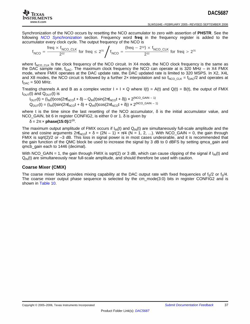
fNCO freq fNCO_CLK
232 for freq 231fNCO (freq 232) fNCO_CLK
232 for freq 231
Coarse Mixer (CMIX)
DAC5687
SLWS164E–FEBRUARY 2005–REVISED SEPTEMBER 2006
Synchronization of the NCO occurs by resetting the NCO accumulator to zero with assertion of PHSTR. See thefollowing NCO Synchronization section. Frequency word freq in the frequency register is added to theaccumulator every clock cycle. The output frequency of the NCO is
where fNCO_CLK is the clock frequency of the NCO circuit. In X4 mode, the NCO clock frequency is the same asthe DAC sample rate, fDAC. The maximum clock frequency the NCO can operate at is 320 MHz – in X4 FMIXmode, where FMIX operates at the DAC update rate, the DAC updated rate is limited to 320 MSPS. In X2, X4Land X8 modes, the NCO circuit is followed by a further 2× interpolation and so fNCO_CLK = fDAC/2 and operates atfDAC = 500 MHz.
Treating channels A and B as a complex vector I + I × Q where I(t) = A(t) and Q(t) = B(t), the output of FMIXIOUT(t) and QOUT(t) is
IOUT(t) = (IIN(t)cos(2πfNCOt + δ) – QIN(t)sin(2πfNCOt + δ)) × 2(NCO_GAIN – 1)
QOUT(t) = (IIN(t)sin(2πfNCOt + δ) + QIN(t)cos(2πfNCOt + δ)) × 2(NCO_GAIN – 1)
where t is the time since the last resetting of the NCO accumulator, δ is the initial accumulator value, andNCO_GAIN, bit 6 in register CONFIG2, is either 0 or 1. δ is given by
δ = 2π × phase(15:0)/216.
The maximum output amplitude of FMIX occurs if IIN(t) and QIN(t) are simultaneously full-scale amplitude and thesine and cosine arguments 2πfNCOt + δ = (2N – 1) × π/4 (N = 1, 2, ...). With NCO_GAIN = 0, the gain throughFMIX is sqrt(2)/2 or –3 dB. This loss in signal power is in most cases undesirable, and it is recommended thatthe gain function of the QMC block be used to increase the signal by 3 dB to 0 dBFS by setting qmca_gain andqmcb_gain each to 1446 (decimal).
With NCO_GAIN = 1, the gain through FMIX is sqrt(2) or 3 dB, which can cause clipping of the signal if IIN(t) andQIN(t) are simultaneously near full-scale amplitude, and should therefore be used with caution.
The coarse mixer block provides mixing capability at the DAC output rate with fixed frequencies of fS/2 or fS/4.The coarse mixer output phase sequence is selected by the cm_mode(3:0) bits in register CONFIG2 and isshown in Table 10.
Copyright © 2005–2006, Texas Instruments Incorporated Submit Documentation Feedback 37
Product Folder Link(s): DAC5687

www.ti.com
Quadrature Modulator Correction (QMC)
DAC5687
SLWS164E–FEBRUARY 2005–REVISED SEPTEMBER 2006
Table 10. Coarse Mixer Sequencescm_mode(3:0) Mixing Mode Sequence
00XX No mixing0100 fDAC/2 DAC A = –A +A –A +A …
DAC B = –B +B –B +B …0101 fDAC/2 DAC A = –A +A –A +A …
DAC B = +B –B +B –B …0110 fDAC/2 DAC A = +A –A +A –A …
DAC B = –B +B –B +B …0111 fDAC/2 DAC A = +A –A +A –A …
DAC B = +B –B +B –B …1000 fDAC/4 DAC A = +A –B –A +B …
DAC B = +B +A –B –A …1001 fDAC/4 DAC A = +A –B –A +B …
DAC B = –B –A +B +A …1010 fDAC/4 DAC A = –A +B +A –B …
DAC B = +B +A –B –A …1011 fDAC/4 DAC A = –A +B +A –B …
DAC B = –B –A +B +A …1100 –fDAC/4 DAC A = +A +B –A –B …
DAC B = +B –A –B +A …1101 –fDAC/4 DAC A = +A +B –A –B …
DAC B = –B +A +B –A …1110 –fDAC/4 DAC A = –A –B +A +B …
DAC B = +B –A –B +A …1111 –fDAC/4 DAC A = –A –B +A +B …
DAC B = –B +A +B –A …
The output of CMIX is complex. For a real output, either DACA or DACB can be used and the other DAC slept,the difference being the phase sequence.
The quadrature modulator correction (QMC) block provides a means for changing the phase balance of thecomplex signal to compensate for I and Q imbalance present in an analog quadrature modulator. The QMC blockis limited in operation to a clock rate of 320 MSPS.
The block diagram for the QMC block is shown in Figure 40. The QMC block contains three programmableparameters. Registers qmc_gain_a and qmc_gain_b control the I and Q path gains and are 11-bit values with arange of 0 to approximately 2. Note that the I and Q gain can also be controlled by setting the DAC full-scaleoutput current (see following). Register qmc_phase controls the phase imbalance between I and Q and is a10-bit value with a range of –1/2 to approximately 1/2.
LO feedthrough can be minimized by adjusting the DAC offset feature described as follows.
An example of sideband optimization using the QMC block and gain adjustment is shown in Figure 41. The QMCphase adjustment in combination with the DAC gain adjustment can reduce the unwanted sideband signal from~40 dBc to > 65 dBc.
Note that mixing in the CMIX block after the QMC correction destroys the I and Q phase compensationinformation from the QMC block.
38 Submit Documentation Feedback Copyright © 2005–2006, Texas Instruments Incorporated
Product Folder Link(s): DAC5687

www.ti.com
Σ
Q(t)
I(t)
11
11
10
qmc_gain_a/210
0, 1/210, ..., 2 – 1/210
X
X
Xqmc_phase/210
–1/2, –1/2 + 1/210, ..., 1/2 – 1/210
qmc_gain_b/210
0, 1/210, ..., 2 – 1/210
B0164−01
L-O
L-O
side-band
side-band
Uncorrected CorrectedC003
DAC Offset Control
DAC5687
SLWS164E–FEBRUARY 2005–REVISED SEPTEMBER 2006
Figure 40. QMC Block Diagram
Figure 41. Example of Sideband Optimization Using QMC Phase and Gain Adjustments
Registers daca_offset and dacb_offset control the I and Q path offsets and are 13-bit values with a range of–4096 to 4095. The DAC offset value adds a digital offset to the digital data before digital-to-analog conversion.The qmc_gain_a and qmc_gain_b registers can be used to back off the signal before the offset to preventsaturation when the offset value is added to the digital signal. The offset values are in 2s-complement format.
It takes four DAC clock cycles to update the 14-bit DAC5687 offset registers. During the first clock cycle, the twoMSBs, daca_offset(13:12) and dacb_offset(13:12), are updated, followed by daca_offset(11:8) anddacb_offset(11:8) on the second clock cycle, daca_offset(7:4) and dacb_offset(7:4) on the third clock cycle, anddaca_offset(3:0) and dacb_offset(3:0) on the fourth clock cycle.
Copyright © 2005–2006, Texas Instruments Incorporated Submit Documentation Feedback 39
Product Folder Link(s): DAC5687

www.ti.com
ΣI
13
daca_offset
–4096, –4095, ..., 4095
B0165−01
ΣQ
13dacb_offset
–4096, –4095, ..., 4095
Analog DAC Gain
Ifullscale 16Vextio
RBIAS GAINCODE 1
16 1 FINEGAIN
3072
Clock Modes
DAC5687
SLWS164E–FEBRUARY 2005–REVISED SEPTEMBER 2006
During the four DAC clock cycles, the partially updated offset register values are summed to the DAC signal.This can result in offset values during the first three DAC clock cycles that are significantly different from thestarting and ending offset values. For example, Table 11 shows the transition from offset value 1023 to 1025.The bit changes in each clock cycle are in bold. As can be seen, the transition between 1023 and 1025 results inoffset values of 1023, 1279, and 1039 during the transition.
Table 11. Offset Values During TransitionDAC Clock Cycle Signed Integer Value Binary Format Hexadecimal Format
0 1023 starting value 00 0011 1111 1111 0x03FF1 1023 00 0011 1111 1111 0x03FF2 1279 00 0100 1111 1111 0x04FF3 1039 00 0100 0000 1111 0x040F4 1025 ending value 00 0100 0000 0001 0x0401
Figure 42. DAC Offset Block
The full-scale DAC output current can be set by programming the daca_gain and dacb_gain registers. The DACgain value controls the full-scale output current.
where GAINCODE = daca_gain(11:8) or dacb_gain(11:8) is the coarse gain setting (0 to 15) and FINEGAIN =daca_gain(7:0) or dacb_gain(7:0) (–128 to 127) is the fine gain setting.
In the DAC5687, the internal clocks (1×, 2×, 4×, and 8× as needed) for the logic, FIR interpolation filters, andDAC are derived from a clock at either the input data rate using an internal PLL (PLL clock mode) or DAC outputsample rate (external clock mode). Power for the internal PLL blocks (PLLVDD and PLLGND) are separate fromthe other clock generation blocks power (CLKVDD and CLKGND), thus minimizing phase noise within the PLL.
The DAC5687 has three clock modes for generating the internal clocks (1×, 2×, 4×, and 8× as needed) for thelogic, FIR interpolation filters, and DACs. The clock mode is set using the PLLVDD pin and dual_clk in registerCONFIG1.
40 Submit Documentation Feedback Copyright © 2005–2006, Texas Instruments Incorporated
Product Folder Link(s): DAC5687

www.ti.com
CLK2
DA[15:0]
DB[15:0]
ts(DATA)
th(DATA)
A0 A1 A2 AN AN+1A3
B0 B1 B2 BN BN+1B3
PLLLOCK
td(PLLLOCK)
T0040-01
CLK2
DA[15:0]
DB[15:0]
ts(DATA)
th(DATA)
A0 A1 A2 AN AN+1A3
B0 B1 B2 BN BN+1B3
PLLLOCK
td(PLLLOCK)
T0040-02
DAC5687
SLWS164E–FEBRUARY 2005–REVISED SEPTEMBER 2006
1. PLLVDD = 0 V and dual_clk = 0: EXTERNAL CLOCK MODE
In EXTERNAL CLOCK MODE, the user provides a clock signal at the DAC output sample rate throughCLK2/CLK2C. CLK1/CLK1C and the internal PLL are not used. The LPF and CLK1/CLK1C pins can be leftunconnected. The input data-rate clock and interpolation rate are selected by the bits interp(1:0) in registerCONFIG0 and is output through the PLLLOCK pin. The PLLLOCK clock can be used to drive the input datasource (such as digital upconverter) that sends the data to the DAC. Note that the PLLLOCK delay relative to theinput CLK2 rising edge (td(PLLLOCK) in Figure 43 and Figure 44) increases with increasing loads. The PLLLOCKoutput driver is not capable of reaching full speed at lower IOVDD voltages. For example, at IOVDD = 1.8 V,PLLLOCK output frequencies > 100 MHz are not recommended. The input data is latched on either the rising(inv_plllock = 0) or falling edge (inv_plllock = 1) of PLLLOCK, which is sensed internally at the output pin.
Figure 43. Dual-Bus Mode Timing Diagram for External Clock Mode (PLLLOCK Rising Edge)
Figure 44. Dual-Bus Mode Timing Diagram for External Clock Mode (PLLLOCK Falling Edge)
2. PLLVDD = 3.3 V (dual_clk can be 0 or 1 and is ignored): PLL CLOCK MODE
In PLL CLOCK MODE, drive the DAC at the input sample rate (unless the data is multiplexed) throughCLK1/CLK1C. CLK2/CLK2C is not used. In this case, there is no phase ambiguity on the clock. The DACgenerates the higher-speed DAC sample-rate clock using an internal PLL/VCO. In PLL clock mode, the userprovides a differential external reference clock on CLK1/CLK1C.
Copyright © 2005–2006, Texas Instruments Incorporated Submit Documentation Feedback 41
Product Folder Link(s): DAC5687

www.ti.com
CLK1
DA[15:0]
DB[15:0]
ts(DATA)th(DATA)
A0 A1 A2 AN AN+1A3
B0 B1 B2 BN BN+1B3
T0039-01
B0053-09
CLKBuffer
CLKBuffer
PFDChargePump VCO
/1
/2
/4
/8
00
01
10
11
1
0
/2
DataLatch
1 ´2
´10
00
01
10
11
/2
/20
1
CLK1
CLK1C
CLK2
LPF pll_div(1:0) PLLVDD
PLLLOCK PLLVDD DA[15:0]DB[15:0]
interl interp(1:0)
fDAC
f /2 X2DAC
f /4DAC X4
f /4DAC X4L
f /8DAC X8
Data
Lock
CLK2C
DAC5687
SLWS164E–FEBRUARY 2005–REVISED SEPTEMBER 2006
A type-four phase-frequency detector (PFD) in the internal PLL compares this reference clock to a feedbackclock and drives the PLL to maintain synchronization between the two clocks. The feedback clock is generatedby dividing the VCO output by 1×, 2×, 4×, or 8× as selected by the prescaler div(1:0). The output of the prescaleris the DAC sample rate clock and is divided down to generate clocks at ÷2, ÷4, and ÷8. The feedback clock isselected by the registers sel(1:0), which is fed back to the PFD for synchronization to the input clock. Thefeedback clock is also used for the data input rate, so the ratio of DAC output clock to feedback clock sets theinterpolation rate of the DAC5687. The PLLLOCK pin is an output indicating when the PLL has achieved lock. Anexternal RC low-pass PLL filter is provided by the user at pin LPF. See the Low-Pass Filter section forfilter-setting calculations. This is the only mode where the LPF filter applies.
Figure 45. Dual-Bus Mode Timing Diagram (PLL Mode)
Figure 46. Clock Generation Architecture in PLL Mode
42 Submit Documentation Feedback Copyright © 2005–2006, Texas Instruments Incorporated
Product Folder Link(s): DAC5687

www.ti.com
talign1
2fCLK2 0.5 ns
th
CLK2
CLK1
DA[15:0]DB[15:0]
∆ < talign
tsT0002−01
th
CLK1
DA[15:0]DB[15:0]
tsT0154−01
Interleave Bus Mode
DAC5687
SLWS164E–FEBRUARY 2005–REVISED SEPTEMBER 2006
3. PLLVDD = 0 V and dual_clk = 1: DUAL CLOCK MODE
In DUAL CLOCK MODE, the DAC is driven at the DAC sample rate through CLK2/CLK2C and the input datarate through CLK1/CLK1C. There are two options in dual clock mode: with FIFO (inv_plllock set) and withoutFIFO (inv_plllock clear). If the FIFO is not used, the CLK1/CLK1C input is used to set the phase of the internalclock divider. In this case, the edges of CLK1 and CLK2 must be aligned to within ±talign (Figure 47), defined as
where fCLK2 is the clock frequency at CLK2. For example, talign = 0.5 ns at fCLK2 = 500 MHz and 1.5 ns at fCLK2 =250 MHz.
If the FIFO is enabled (inv_plllock set) in dual clock mode, then CLK1 is only used as an input latch (Figure 48),is independent from the internal divided clock generated from CLK2/CLK2C, and there is no alignmentspecification. However, the FIFO must be synchronized by one of the methods listed in the SYNC_CNTLregister, and the latency of the DAC can be up to one clock cycle different, depending on the phase relationshipbetween CLK1 and the internally divided clock.
Figure 47. Dual Clock Mode Without FIFO
Figure 48. Dual Clock Mode With FIFO
The CDC7005 from Texas Instruments is recommended for providing phase-aligned clocks at differentfrequencies for this application.
In interleave bus mode, one parallel data stream with interleaved data (I and Q) is input to the DAC5687 on databus DA. Interleave bus mode is selected by setting INTERL to 1 in the config_msb register. Figure 49 showsthe DAC5687 data path in interleave bus mode. The interleave bus mode timing diagram is shown in Figure 50.
Copyright © 2005–2006, Texas Instruments Incorporated Submit Documentation Feedback 43
Product Folder Link(s): DAC5687
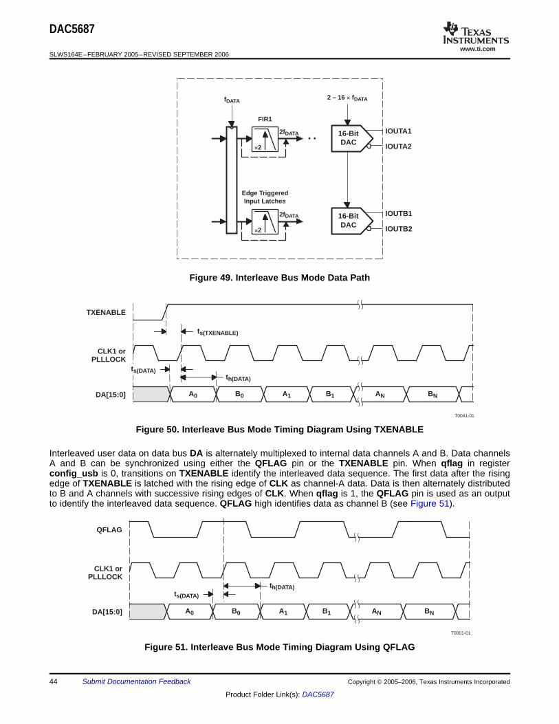
www.ti.com
IOUTB1
IOUTB2
IOUTA1
IOUTA2
16-BitDAC
2fDATA
2 – 16 fDATAfDATA
2
16-BitDAC
2fDATA
2
FIR1
Edge TriggeredInput Latches
• • •
• • •
DA[15:0]
DEMUX
B0025-02
DA[15:0]
ts(DATA)th(DATA)
A0 B0 A1 AN BNB1
TXENABLE
ts(TXENABLE)
CLK1 orPLLLOCK
T0041-01
DA[15:0]
ts(DATA)
th(DATA)
A0 B0 A1 AN BNB1
QFLAG
CLK1 orPLLLOCK
T0001-01
DAC5687
SLWS164E–FEBRUARY 2005–REVISED SEPTEMBER 2006
Figure 49. Interleave Bus Mode Data Path
Figure 50. Interleave Bus Mode Timing Diagram Using TXENABLE
Interleaved user data on data bus DA is alternately multiplexed to internal data channels A and B. Data channelsA and B can be synchronized using either the QFLAG pin or the TXENABLE pin. When qflag in registerconfig_usb is 0, transitions on TXENABLE identify the interleaved data sequence. The first data after the risingedge of TXENABLE is latched with the rising edge of CLK as channel-A data. Data is then alternately distributedto B and A channels with successive rising edges of CLK. When qflag is 1, the QFLAG pin is used as an outputto identify the interleaved data sequence. QFLAG high identifies data as channel B (see Figure 51).
Figure 51. Interleave Bus Mode Timing Diagram Using QFLAG
44 Submit Documentation Feedback Copyright © 2005–2006, Texas Instruments Incorporated
Product Folder Link(s): DAC5687

www.ti.com
Input FIFO
B0166-01
0
1S
0
1 D Q
InputPointer
Generation
PLLLOCK
MUX
CLK1
CLK1C
PLLVDD, inv_plllock, dual_clk
MUX
ClockGenerator
ResynchonizedDA[15:0], DB[15:0]and PHSTR
sync sourceTXENABLE, PHSTR, QFLAG, DB[15],DA[15] oneshot, SIF write, always off
CLK2
CLK2C
PLL VCO
1
fifo_bypass
in_sel_d
in_sel_c
in_sel_b
in_sel_a
q_b
q_c
q_d
q_in
q_out
clk_in clk_out
sel_q_a
sel_q_d
sel_q_c
sel_q_b
sync
D QDA[15:0],DB[15:0],
PHSTR
0
1
S
D Q
S
0
1
S
D Q
QD0
QD
S
q_a
OutputPointer
Generation
DAC5687
SLWS164E–FEBRUARY 2005–REVISED SEPTEMBER 2006
When using interleaved input mode with the PLL enabled, input clock CLK1 is at 2× the frequency of the input toFIR1. If the dividers for multiple DAC5687s are not synchronized, there can be a one-CLK1-period output timedifference between devices that have synchronized input data. However, the divider that generates the clock forthe FIR1 input is not connected to the DAC5687 synchronization circuitry. In general, dual-clock mode isrecommended in applications where multiple DAC5687s must be synchronized in interleaved input mode. If PLLmode is required, the following workaround using the asynchronous RESET pin synchronizes the clock dividers.With the CLK1 input off and the chip powered, set RESET low for >50 ns and then high for all devices,simultaneously restarting CLK1. Note that the devices must be reprogrammed after the reset sequence. If CLK1is kept active during the reset sequence, then multiple devices are typically reset to the same clock phase, butbecause the RESET pin is asynchronous, the clock divider on two devices can come out of reset at slightlydifferent times.
In external clock mode, where the DAC5687 is clocked at the DAC update rate, the DAC5687 has an optionalinput FIFO that allows latching of DA[15:0], DB[15:0] and PHSTR based on a user-provided CLK1/CLK1C inputor the input data rate clock provided to the PLLLOCK pin. The FIFO can be bypassed by setting registerfifo_bypass in CONFIG0 to 1.
The input interface FIFO incorporates a four-sample register file, an input pointer, and an output pointer.Initialization of the FIFO pointers can be programmed to one of seven different sources.
Figure 52. DAC5687 Input FIFO Logic
Copyright © 2005–2006, Texas Instruments Incorporated Submit Documentation Feedback 45
Product Folder Link(s): DAC5687

www.ti.com
PHSTR
QD
QFLAG
TXENABLE
DB[15]
DA[15]QD
PLLLOCK
MUX
CLK1
CLK1C
clk_in
MUX
D
PLL VCOclk_out
sync
sync_fifo(2:0)
1
000
001
010
011
100
101
110
111
Q
resync_fifo_in
CLK2
CLK2C
B0167-01
resync_fifo_out1
0
QD
QD
QD
QD
D Q D Q D QD Q
D Q D Q D QD Q
ClockGenerator
PLLVDD, inv_plllock, dual_clk
sync_fifo = “100”DA[15] First Rising Edge
DAC5687
SLWS164E–FEBRUARY 2005–REVISED SEPTEMBER 2006
Initialization of the FIFO block involves selecting and asserting a synchronization source. Initialization causes theinput and output pointers to be forced to an offset of 2; the input pointer is forced to the in_sel_a state, while theoutput pointer is forced to the sel_q_c state. This initialization of the input and output pointers can causediscontinuities in a data stream and should therefore be handled at startup.
Table 12. Synchronization Source Selectionsync_fifo(2:0) Synchronization Source
000 TXENABLE pin001 PHSTR pin010 QFLAG pin011 DB[15]100 DA[15] first transition (one shot)101 Sync now with SIF write (always on)110 Sync source disabled (always off)111 Sync now with SIF write (always on)
All possible sync sources are registered with clk_in and then passed through a synchronous rising edge detector.
Figure 53. DAC5687 FIFO Synchronization Source Logic
For example, if TXENABLE is selected as the sync source, a low-to-high transition on the TXENABLE pin causesthe pointers to be initialized.
46 Submit Documentation Feedback Copyright © 2005–2006, Texas Instruments Incorporated
Product Folder Link(s): DAC5687

www.ti.com
Even/Odd Input Mode
Synchronization
NCO Synchronization
DAC5687
SLWS164E–FEBRUARY 2005–REVISED SEPTEMBER 2006
Once initialized, the FIFO input pointer advances using clk_in and the output pointer advances using clk_out,providing an elastic buffering effect. The phase relationship between clk_in and clk_out can wander or drift untilthe output pointer overruns the input pointer or vice versa.
The DAC5687 has a double data rate input mode that allows both input ports to be used to multiplex data ontoone DAC channel (A). In the even/odd mode, the FIR3 filter can be used to interpolate the data by 2×. Theeven/odd input mode is enabled by setting half_rate in CONFIG3. The maximum input rate for each port is 250MSPS, for a combined rate of 500 MSPS.
The DAC5687 has several digital circuits that can be synchronized to a known state. The circuits that can besynchronized are the fine mixer (NCO), coarse mixer (fixed fS/2 or fS/4 mixer), the FIFO input and outputpointers, and the internal clock divider.
Table 13. Synchronization in Different Clock ModesSerial Interface Register Bits DA, DB,
Clock PLLVDD PHSTR, and DescriptionMode Pin TXENABLEfifo_bypass dual_clk inv_plllockLatch
Single 0 V 1 0 0 PLLLOCK Signal at the PLLLOCK output pin is used to clock theexternal rising edge PHSTR signal into the chip. The PLLLOCK output
clock clock is generated by dividing the CLK2/CLK2C input1 PLLLOCKwithout signal by the programmed interpolation and interfacefalling edgeFIFO settings.Single 0 V 0 0 0 PLLLOCK Signal at the PLLLOCK output pin is used to clock the
external rising edge PHSTR signal into the chip. The PLLLOCK outputclock with clock is generated by dividing the CLK2/CLK2C input1 PLLLOCKFIFO signal by the programmed interpolation and interfacefalling edge settings. Enabling the FIFO allows the chip to function
with large loads on the PLLLOCK output pin at highinput rates. The FIFO must be initialized first in thismode.
Dual 0 V 1 1 0 CLK1/CLK1C The CLK1/CLK1C input signal is used to clock in theexternal PHSTR signal. CLK1/CLK1C and CLK2/CLK2C are
clock both input to the chip, and the phase relationshipwithout must be tightly controlled.FIFODual 0 V 0 1 1 CLK1/CLK1C The CLK1/CLK1C input signal is used to clock in the
external PHSTR signal. CLK1/CLK1C and CLK2/CLK2C areclock with both input to the chip, but no phase relationship is
FIFO required. The FIFO input circuits are used to managethe clock domain transfers. The FIFO must beinitialized in this mode.
PLL 3.3 V 1 0 0 CLK1/CLK1C The CLK1/CLK1C input signal is used to clock in theenabled PHSTR signal. The FIFO must be bypassed when the
PLL is enabled.
The phase accumulator in the NCO block (see the Fine Mixer (FMIX) section and Figure 39 for a description ofthe NCO) can be synchronously reset when PHSTR is asserted. The PHSTR signal passes through the inputFIFO block, using the input clock associated with the clocking mode. If the FIFO is enabled, there can be someuncertainty in the exact instant the PHSTR synchronization signal arrives at the NCO accumulator due to theelastic capabilities of the FIFO. For example, in dual-clock mode with the FIFO enabled, the internal clockgenerator divides down the CLK2/CLK2C input signal to generate the FIFO output clock. The phase of thisgenerated clock is unknown externally, resulting in an uncertainty of the exact PHSTR instant of as much as afew input clock cycles.
Copyright © 2005–2006, Texas Instruments Incorporated Submit Documentation Feedback 47
Product Folder Link(s): DAC5687

www.ti.com
B0168-01
PHSTR
PLLLOCK
MUX
CLK1
CLK1C
PLLVDD, inv_plllock, dual_clk
clk_in
ClockGenerator CLK2
CLK2C
clk_out
FIFO
PHSTR Syncto NCO
PLL VCOclk_nco
PhaseAccumulatorResetQD QD QD QD QD
QD
T0156-01
PHSTR
clk_in
clk_out
phstr at FIFOOutput
clk_nco
PhaseA
Rccumulator
eset
phase_accum
Only Must Be Asserted for One clk_in Period
Input Delay Line + FIFO Delay
13 clk_nco Cycles
DAC5687
SLWS164E–FEBRUARY 2005–REVISED SEPTEMBER 2006
Figure 54. Logic Path for PHSTR Synchronization Signal to NCO
The serial interface includes a sync_nco bit in register SYNC_CNTL, which must be set for the PHSTR inputsignal to initialize the phase accumulator.
The NCO uses a rising edge detector to perform the synchronous reset of the phase accumulator. Due to thepipelined nature of the NCO, the latency from the phstr sync signal at the FIFO output to the instant the phaseaccumulator is cleared is 13 fNCO clock cycles (fNCO = fDAC in X4 mode, fNCO = fDAC/2 in X2, X4L, and X8 modes).In 2× interpolation mode with the inverse sinc filter disabled, overall latency from PHSTR input to DAC output is~100 input clock cycles.
Figure 55. NCO Phase Accumulator Reset Synchronization Timing
48 Submit Documentation Feedback Copyright © 2005–2006, Texas Instruments Incorporated
Product Folder Link(s): DAC5687

www.ti.com
Coarse Mixer (CMIX) Synchronization
B0169-01
PHSTR
PLLLOCK
MUX
CLK1
CLK1C
PLLVDD, inv_plllock, dual_clk
clk_in
ClockGenerator CLK2
CLK2C
clk_out
FIFO
PHSTR Sync toCoarse Mixer
PLL VCOclk_cmix
SequencerReset
QD QD QDQD QD
QD
sync_cm
DAC5687
SLWS164E–FEBRUARY 2005–REVISED SEPTEMBER 2006
The coarse mixer implements the fDAC/2 and fDAC/4 (and –fDAC/4) fixed complex mixing operation using simplecomplements of the data-path signals to create the proper sequences. The sequences are controlled using asimple counter, and this counter can be synchronously reset using the PHSTR signal.
Similar to the NCO, the PHSTR signal used by the coarse mixer is from the FIFO output. This introduces thesame uncertainty effect due to the FIFO input-to-output pointer relationship. Bypassing the FIFO and using thedual external clock mode without FIFO eliminates this uncertainty for systems using multiple DAC5687 deviceswhen this cannot be tolerated. Using the internal PLL, as with the NCO, allows the complete control andsynchronization of the coarse mixer.
Figure 56. Logic Path for PHSTR Synchronization Signal to CMIX Reset
To enable the PHSTR synchronous reset, the serial interface bit sync_cm in register SYNC_CNTL must be set.The coarse mixer sequence counter is held in reset when PHSTR is low and operates when PHSTR is high.
Copyright © 2005–2006, Texas Instruments Incorporated Submit Documentation Feedback 49
Product Folder Link(s): DAC5687

www.ti.com
T0155-01
PHSTR
clk_in
clk_out
phstr at FIFOOutput
clk_cmix
Sequencerfs/2
Only Must Be High for One clk_in Period
Input Delay Line + FIFO Delay
0 180
90
0 180
0 18090 270 0Sequencer
fs/4
SequencerReset
Input Clock Synchronization of Multiple DAC5687s
DAC5687
SLWS164E–FEBRUARY 2005–REVISED SEPTEMBER 2006
Figure 57. CMIX Reset Synchronization Timing
In addition to the reset function provided by the PHSTR signal, the phstr_del(1:0) bits in register ATEST allowthe user to select the initial (reset) state. Changing the cm_mode lower 2 bits produces the same phase shiftresults.
Table 14. Initial State of CMIX After ResetFix Mix Selection phstr_del(1:0) Initial State at PHSTR
fS/2 00 and 10 NormalfS/2 01 and 11 180-degree shiftfS/4 00 NormalfS/4 01 90-degree shiftfS/4 10 180-degree shiftfS/4 11 270-degree shift
For applications where multiple DAC5687 chips are used, clock synchronization is best achieved by usingdual-clock mode with the FIFO disabled or the PLL-clock mode. In the dual-clock mode with FIFO disabled, anappropriate clock PLL such as the CDC7005 is required to provide the DAC and input rate clocks that meet theskew requirement talign (see Figure 47). An example for synchronizing multiple DAC5687 devices in dual clockmode with two CDC7005s is shown in Figure 58. When using the internal PLL-clock mode, synchronization ofmultiple using PHSTR is completely deterministic due to the phase/frequency detector in the PLL feedback loop.All chips using the same CLK1/CLK1C input clock have identical internal clocking phases.
50 Submit Documentation Feedback Copyright © 2005–2006, Texas Instruments Incorporated
Product Folder Link(s): DAC5687

www.ti.com
Y0
Y0
Y0
Y0
Y1
Y1
Y1
Y1
Y2
Y2
Y2
Y2
Y3
Y3
Y3
Y3
CLK1
CLK1
CLK1C
CLK1C
CLK2
CLK2
CLK2C
CLK2C
CLK1
CLK1
CLK1C
CLK1C
CLK2
CLK2
CLK2C
CLK2C
Ref
Ref
B0170-01
fINPUT
fINPUT
fINPUT
fDAC
fDAC
fDAC
fDAC
fINPUT
fINPUT
CDC7005
#1
CDC7005
#2
DAC5687
#1
DAC5687
#3
DAC5687
#2
DAC5687
#4
Reference Operation
DAC Transfer Function
DAC5687
SLWS164E–FEBRUARY 2005–REVISED SEPTEMBER 2006
Figure 58. Block Diagram for Clock Synchronization of Multiple DAC5687 Devices in Dual-Clock Mode
The DAC5687 comprises a band-gap reference and control amplifier for biasing the full-scale output current. Thefull-scale output current is set by applying an external resistor RBIAS to pin BIASJ. The bias current IBIAS throughresistor RBIAS is defined by the on-chip band-gap reference voltage and control amplifier. The full-scale outputcurrent equals 16 times this bias current. The full-scale output current IOUTFS can thus be expressed as:
IOUTFS = 16 × IBIAS = 16 × VEXTIO / RBIAS
where VEXTIO is the voltage at terminal EXTIO. The band-gap reference voltage delivers an accurate voltage of1.2 V. This reference is active when terminal EXTLO is connected to AGND. An external decoupling capacitorCEXT of 0.1 µF should be connected externally to terminal EXTIO for compensation. The band-gap reference canadditionally be used for external reference operation. In that case, an external buffer with high-impedance inputshould be applied in order to limit the band-gap load current to a maximum of 100 nA. The internal reference canbe disabled and overridden by an external reference by connecting EXTLO to AVDD. Capacitor CEXT may hencebe omitted. Terminal EXTIO thus serves as either input or output node.
The full-scale output current can be adjusted from 20 mA down to 2 mA by varying resistor RBIAS or changing theexternally applied reference voltage. The internal control amplifier has a wide input range, supporting thefull-scale output current range of 20 mA.
The CMOS DACs consist of a segmented array of NMOS current sinks, capable of sinking a full-scale outputcurrent up to 20 mA. Differential current switches direct the current of each current source through either one ofthe complementary output nodes IOUT1 or IOUT2. Complementary output currents enable differential operation,thus canceling out common-mode noise sources (digital feedthrough, on-chip and PCB noise), dc offsets,even-order distortion components, and increasing signal output power by a factor of two.
Copyright © 2005–2006, Texas Instruments Incorporated Submit Documentation Feedback 51
Product Folder Link(s): DAC5687

www.ti.com
Analog Current Outputs
DAC5687
SLWS164E–FEBRUARY 2005–REVISED SEPTEMBER 2006
The full-scale output current is set using external resistor RBIAS in combination with an on-chip band-gap voltagereference source (1.2 V) and control amplifier. Current IBIAS through resistor RBIAS is mirrored internally to providea full-scale output current equal to 16 times IBIAS. The full-scale current IOUTFS can be adjusted from 20 mAdown to 2 mA.
The relation between IOUT1 and IOUT2 can be expressed as:
IOUT1 = –IOUTFS – IOUT2
Current flowing into a node is denoted as – current, and current flowing out of a node as + current. Because theoutput stage is a current sink, the current can only flow from AVDD into the IOUT1 and IOUT2 pins. If IOUT2 =–5 mA and IOUTFS = 20 mA then:
IOUT1 = –20 – (–5) = –15 mA
The output current flow in each pin driving a resistive load can be expressed as:
IOUT1 = IOUTFS × CODE / 65,536
IOUT2 = IOUTFS × (65,535 – CODE) / 65,536
where CODE is the decimal representation of the DAC data input word.
For the case where IOUT1 and IOUT2 drive resistor loads RL directly, this translates into single-ended voltagesat IOUT1 and IOUT2:
VOUT1 = AVDD – | IOUT1 | × RL
VOUT2 = AVDD – | IOUT2 | × RL
Assuming that the data is full scale (65,535 in offset binary notation) and RL is 25 Ω, the differential voltagebetween pins IOUT1 and IOUT2 can be expressed as:
VOUT1 = AVDD – | –20 mA | × 25 Ω = 2.8 V
VOUT2 = AVDD – | –0 mA | × 25 Ω = 3.3 V
VDIFF = VOUT1 – VOUT2 – 0.5 V
Note that care should be taken not to exceed the compliance voltages at node IOUT1 and IOUT2, which wouldlead to increased signal distortion.
Figure 59 shows a simplified schematic of the current source array output with corresponding switches.Differential switches direct the current of each individual NMOS current source to either the positive output nodeIOUT1 or its complementary negative output node IOUT2. The output impedance is determined by the stack ofthe current sources and differential switches, and is typically >300 kΩ in parallel with an output capacitance of5 pF.
The external output resistors are referred to AVDD. The minimum output compliance at nodes IOUT1 and IOUT2is limited to AVDD – 0.5 V. The maximum output compliance voltage at nodes IOUT1 and IOUT2 equals AVDD +0.5 V. Beyond this value, transistor breakdown may occur, resulting in reduced reliability of the DAC5687 device.Exceeding the minimum output compliance voltage adversely affects distortion performance and integralnonlinearity. The optimum distortion performance for a single-ended or differential output is achieved when themaximum full-scale signal at IOUT1 and IOUT2 is in the range of AVDD ±0.5 V.
52 Submit Documentation Feedback Copyright © 2005–2006, Texas Instruments Incorporated
Product Folder Link(s): DAC5687

www.ti.com
IOUT1 IOUT2
S(1) S(1)C
RLOAD RLOAD
S(2) S(2)C S(N) S(N)C
AVDD
S0032-01
IOUT11:1
IOUT2
50 Ω
50 Ω
RLOAD50 Ω100 Ω
AVDD (3.3 V)
AVDD (3.3 V)S0033-01
DAC5687
SLWS164E–FEBRUARY 2005–REVISED SEPTEMBER 2006
Figure 59. Equivalent Analog Current Output
The DAC5687 can be easily configured to drive a doubly terminated 50-Ω cable using a properly selected RFtransformer. Figure 60 and Figure 61 show the 50-Ω doubly terminated transformer configuration with 1:1 and4:1 impedance ratio, respectively. Note that the center tap of the primary input of the transformer must beconnected to AVDD to enable a dc current flow. Applying a 20-mA full-scale output current would lead to a0.5-VPP output for a 1:1 transformer and a 1-VPP output for a 4:1 transformer. The low dc impedance between theIOUT1 or IOUT2 and the transformer center tap sets the center of the ac signal at AVDD, so the 1-VPP output forthe 4:1 transformer results in an output between AVDD + 0.5 V and AVDD – 0.5 V.
Figure 60. Driving a Doubly Terminated 50-Ω Cable Using a 1:1 Impedance Ratio Transformer
Copyright © 2005–2006, Texas Instruments Incorporated Submit Documentation Feedback 53
Product Folder Link(s): DAC5687

www.ti.com
IOUT14:1
IOUT2
100 Ω
100 Ω
RLOAD50 Ω
AVDD (3.3 V)
AVDD (3.3 V)S0033-02
Combined Output Termination
S0069-01
IOUTA11:1
RLOAD50 Ω
IOUTA2
AVDD (3.3 V)IOUTB1
IOUTB2
DAC5687
SLWS164E–FEBRUARY 2005–REVISED SEPTEMBER 2006
Figure 61. Driving a Doubly Terminated 50-Ω Cable Using a 4:1 Impedance Ratio Transformer
The DAC5687 DAC A and DAC B outputs can be summed together as shown in Figure 62 to provide a 40-mAfull-scale output for increased output power.
Figure 62. Combined Output Termination Using a 1:1 Impedance Ratio Transformer Into 50-Ω Load
For the case where the digital codes for the two DACs are identical, the termination results in a full-scale swingof 2 VPP into the 50-Ω load, or 10 dBm. This is 6 dB higher than the 4:1 output termination recommended for asingle DAC output.
There are two methods to produce identical DAC codes. In modes where there is mixing between digitalchannels A and B, i.e., when channels A and B are isolated, the identical data can be sent to both input ports toproduce identical DAC codes. Channels A and B are isolated when FMIX is disabled, the QMC is disabled orenabled with QMC phase register set to 0, and CMIX is disabled or set to fDAC/2. Note that frequencyupconversion is still possible using the high-pass filter setting and CMIX fDAC/2.
Alternatively, by applying the input data on one input port only and setting the other input port to midscale (zero),the NCO can be used to duplicate the output of the active input channel in the other channel by setting thefrequency to zero, phase to 8192 and NCO_GAIN = 1 and QMC gain = 1446. Assuming I(t) is the wanted signaland Q(t) = 0, this is demonstrated by the simplification of the NCO equations in the Fine Mixer (FMIX) section:
IOUT(t) = (IIN(t)cos(2π × 0 × t + π/4) – 0 × sin(2π × 0 × t + π/4) × 2(1 – 1) = IIN(t)cos(π/4) = IIN(t)/2½
54 Submit Documentation Feedback Copyright © 2005–2006, Texas Instruments Incorporated
Product Folder Link(s): DAC5687

www.ti.com
Digital Inputs
DA[15:0]DB[15:0]
SLEEPPHSTR
TXENABLEQFLAG
SDIOSCLK
SDENB
InternalDigital In
IOVDD
IOGND
RESETB InternalDigital In
IOVDD
IOGNDS0027-01
Clock Inputs
CLK
InternalDigital In
CLKC
CLKGND
R110 kΩ
CLKVDD
R110 kΩ
R210 kΩ
R210 kΩ
CLKVDD CLKVDD
S0028-01
DAC5687
SLWS164E–FEBRUARY 2005–REVISED SEPTEMBER 2006
QOUT(t) = (IIN(t)sin(2π × 0 × t + π/4) + 0 × cos(2π × 0 × t + π/4)) × 2(1 – 1) = IIN(t)sin(π/4) = IIN(t)/2½
Applying the QMC gain of 1446, equivalent to 2½, increases the signal back to unity gain through the FMIX andthe QMC blocks.
Note that with this termination, the DAC side of the transformer is not 50-Ω terminated and therefore may resultin reflections when used with a cable output.
Figure 63 shows a schematic of the equivalent CMOS digital inputs of the DAC5687. DA[15:0], DB[15:0], SLEEP,PHSTR, TXENABLE, QFLAG, SDIO, SCLK, and SDENB have pulldown resistors and RESETB has a pullupresistor internal to the DAC5687. See the specification table for logic thresholds. The pullup and pulldowncircuitry is approximately equivalent to 100 kΩ.
Figure 63. CMOS/TTL Digital Equivalent Input
Figure 64 shows an equivalent circuit for the clock input.
Figure 64. Clock Input Equivalent Circuit
Figure 65, Figure 66, and Figure 67 show various input configurations for driving the differential clock input(CLK/CLKC).
Copyright © 2005–2006, Texas Instruments Incorporated Submit Documentation Feedback 55
Product Folder Link(s): DAC5687

www.ti.com
RT200 Ω
CLK1:4
CLKC
Termination Resistor
Swing Limitation
Optional, May Be Bypassedfor Sine Wave Input
CAC0.1 µF
S0029-01
Ropt22 Ω
CLK1:1
CLKCOptional, ReducesClock Feedthrough
CAC0.01 µF
TTL/CMOSSource
Ropt22 Ω
CLK
CLKC
Node CLKC Internally Biasedto CLKVDD2
TTL/CMOSSource
0.01 µF
S0030-01
RT130 Ω
CAC0.1 µF
CAC0.1 µF
RT130 Ω
VTT
DifferentialECL
or(LV)PECL
Source
+
–
CLK
CLKC
RT82.5 Ω
RT82.5 Ω
100 Ω
S0031-01
DAC5687
SLWS164E–FEBRUARY 2005–REVISED SEPTEMBER 2006
Figure 65. Clock Input Configuration Using 50-Ω Cable Input
Figure 66. Driving the DAC5687 With a Single-Ended TTL/CMOS Clock Source
Figure 67. Driving the DAC5687 With Differential ECL/PECL Clock Source
56 Submit Documentation Feedback Copyright © 2005–2006, Texas Instruments Incorporated
Product Folder Link(s): DAC5687

www.ti.com
Power-Up Sequence
Sleep Mode
APPLICATION INFORMATION
Designing the PLL Loop Filter
DAC5687
SLWS164E–FEBRUARY 2005–REVISED SEPTEMBER 2006
In all conditions, bring up DVDD first. If PLLVDD is powered (PLL on), CLKVDD should be powered before orsimultaneously with PLLVDD. AVDD, CLKVDD, and IOVDD can be powered simultaneously or in any order.Within AVDD, the multiple AVDD pins should be powered simultaneously.
There are no specific requirements on the ramp rate for the supplies.
The DAC5687 features a power-down mode that turns off the output current and reduces the supply current toless than 5 mA over the supply range of 3 V to 3.6 V and temperature range. The power-down mode is activatedby applying a logic level 1 to the SLEEP pin (e.g., by connecting pin SLEEP to AVDD). An internal pulldowncircuit at node SLEEP ensures that the DAC5687 is enabled if the input is left disconnected. Power-up andpower-down activation times depend on the value of external capacitor at node EXTIO. For a nominal capacitorvalue of 0.1 µF, power down takes less than 5 µs and approximately 3 ms to power back up.
Table 15. Optimum DAC5687 PLL SettingsfDAC (MHz) pll_freq pll_kv pll_div(1:0) fVCO/fDAC Estimated GVCO (MHz/V)
25 to 28.125 0 0 11 8 38028.125 to 46.25 0 1 11 8 250
46.25 to 60 0 0 11 8 30060 to 61.875 1 1 11 8 13061.875 to 65 1 0 11 8 225
65 to 92.5 0 1 10 4 25092.5 to 120 0 0 10 4 300
120 to 123.75 1 1 10 4 130123.75 to 130 1 0 10 4 225
130 to 185 0 1 01 2 250185 to 240 0 0 01 2 300
240 to 247.5 1 1 01 2 130247.5 to 260 1 0 01 2 225260 to 370 0 1 00 1 250370 to 480 0 0 00 1 300480 to 495 1 1 00 1 130495 to 520 1 0 00 1 225
The optimized DAC5687 PLL settings based on the VCO frequency MIN and MAX values (see the digitalspecifications) as a function of fDAC are listed in Table 15. To minimize phase noise at a given fDAC, pll_freq,pll_kv, and pll_div have been chosen so GVCO is minimized and within the MIN and MAX frequency for a givensetting.
For example, if fDAC = 245.76 MHz, pll_freq is set to 1, pll_kv is set to 0 and pll_div(1:0) is set to 01 (divideby 2) to lock the VCO at 491.52 MHz.
The external loop filter components C1, C2, and R1 are set by the GVCO, N = fVCO/fDATA = fVCO ×Interpolation/fDAC, the loop phase margin φd and the loop bandwidth ωd. Except for applications where abruptclock frequency changes require a fast PLL lock time, it is suggested that φd be set to at least 80 degrees forstable locking and suppression of the phase-noise side lobes. Phase margins of 60 degrees or less can besensitive to board layout and decoupling details.
C1, C2, and R1 are then calculated by the following equations
Copyright © 2005–2006, Texas Instruments Incorporated Submit Documentation Feedback 57
Product Folder Link(s): DAC5687

www.ti.com
C1 11 23 C2 1 2
3R1 32
1 (3 2)
1 KdKvco
2d
tand secd 2 1
dtand secd
3
tand secdd
DAC5687 Passive Interface to Analog Quadrature Modulators
DAC5687
SLWS164E–FEBRUARY 2005–REVISED SEPTEMBER 2006
where,
andcharge pump current: iqp = 1 mAvco gain: KVCO = 2π × GVCO rad/VFVCO/FDATA: N = 2, 4, 8, 16, 32phase detector gain: Kd = iqp × (2 × N) – 1 A/rad
An Excel™ spreadsheet is provided by Texas Instruments for automatically calculating the values for C1, C2,and R.
Completing the example given previously with:Parameter Value Units
GVCO 1.30E+02 MHz/Vωd 0.50E+00 MHzN 4φd 80 Degrees
The component values are:C1 (F) C2 (F) R (Ω)
3.74E–08 2.88E–10 9.74E+01
As the PLL characteristics are not sensitive to these components, the closest 20% tolerance capacitor and 1%tolerance resistor values can be used. If the calculation results in a negative value for C2 or an unrealisticallylarge value for C1, then the phase margin may need to be reduced slightly.
The DAC5687 has a maximum 20-mA full-scale output and a compliance range of AVDD ±0.5 V. The TRF3701or TRF3702 analog quadrature modulators (AQM) require a common mode of approximately 3.7 V and 1.5 V to2-VPP differential swing. A resistive network as shown in Figure 68 can be used to translate the common-modevoltage between the DAC5687 and TRF3701 or TRF3702. The voltage at the DAC output pins for a full-scalesine wave is centered at approximately AVDD with a 1-VPP single-ended (2-VPP differential) swing. The voltage atthe TRF3701/2 input pins is centered at 3.7 V and swings 0.76-VPP single-ended (1.52-VPP differential), or 2.4 dBof insertion loss.
58 Submit Documentation Feedback Copyright © 2005–2006, Texas Instruments Incorporated
Product Folder Link(s): DAC5687

www.ti.com
B0046-01
TRF3701TRF3702
GND
205 Ω 205 Ω15.4 Ω
15.4 Ω
15.4 Ω
15.4 Ω
GND
205 Ω 205 Ω
5 V
50 Ω 50 Ω
5 V
50 Ω 50 Ω
B0046-02
AQM
205 Ω 205 Ω
205 Ω 205 Ω
5 V
66.5 Ω 66.5 Ω
5 V
66.5 Ω 66.5 Ω
0 V
0 V
Nonharmonic Clock-Related Spurious Signals
DAC5687
SLWS164E–FEBRUARY 2005–REVISED SEPTEMBER 2006
Figure 68. DAC5687 Passive Interface to TRF3701/2 Analog Quadrature Modulator
Changing the voltage levels and resistor values enables other common-mode voltages at the analog quadraturemodulator input. For example, the network shown in Figure 69 can produce a 3.3-V common mode for theTRF3703-33, with a 0.96-VPP single-ended swing (1.56-VPP differential swing).
Figure 69. DAC5687 Passive Interface to TRF3703-33 Analog Quadrature Modulator
In interpolating DACs, imperfect isolation between the digital and DAC clock circuits generates spurious signalsat frequencies related to the DAC clock rate. The digital interpolation filters in these DACs run at subharmonicfrequencies of the output rate clock, where these frequencies are fDAC/2N, N = 1 – 3. For example, for X2 modethere is only one interpolation filter running at fDAC/2; for X4 and X4L modes, on the other hand, there are twointerpolation filters running at fDAC/2 and fDAC/4. In X8 mode, there are three interpolation filters running at fDAC/2,fDAC/4, and fDAC/8. These lower-speed clocks for the interpolation filter mix with the DAC clock circuit and createspurious images of the wanted signal and second Nyquist-zone image at offsets of fDAC/2N.
Copyright © 2005–2006, Texas Instruments Incorporated Submit Documentation Feedback 59
Product Folder Link(s): DAC5687

www.ti.com
Location of the Spurious Signals
fSIG/fDAC
−0.5
−0.4
−0.3
−0.2
−0.1
−0.0
0.1
0.2
0.3
0.4
0.5
0.0 0.1 0.2 0.3 0.4 0.5
Spu
rious
Fre
quen
cy/f
DA
C
G026
fSIG
fSIG − fDAC/2
(a) Complex Output in X2 Mode (b) Real Output in X2 Mode
fSIG/fDAC
0.00
0.05
0.10
0.15
0.20
0.25
0.30
0.35
0.40
0.45
0.50
0.0 0.1 0.2 0.3 0.4 0.5
Spu
rious
Fre
quen
cy/f
DA
C
G027
fSIG
fSIG − fDAC/2
DAC5687
SLWS164E–FEBRUARY 2005–REVISED SEPTEMBER 2006
To calculate the nonharmonic clock-related spurious signals for a particular condition, we first determine thelocation of the spurious signals and then the amplitude.
The location of the spurious signals is determined by the DAC5687 output frequency (fSIG) and whether theoutput is used as a dual-output complex signal to be fed to an analog quadrature modulator (AQM) or as a realIF signal from a single DAC output.
Figure 70 shows the location of spurious signals for X2 mode as a function of fSIG/fDAC. For complex outputs, thespurious frequencies cover a range of –0.5 × fDAC to 0.5 × fDAC, with the negative complex frequency indicatingthat the spurious signal falls in the opposite sideband from the wanted signal at the output of the AQM. For thereal output, the phase information for the spurious signal is lost, and therefore what was a negative frequency forthe complex output is a positive frequency for a real output.
For the X2 mode, there is one spurious frequency with an absolute frequency less than 0.5 × fDAC. For a complexoutput in X2 mode, the spurious signal always is offset fDAC/2 from the wanted signal at fSIG – fDAC/2. For a realoutput, as fSIG approaches fDAC/4, the spurious signal frequency falls at fDAC/2 – fSIG, which also approachesfDAC/4.
Figure 70. Frequency of Clock Mixing Spurious Images in X2 Mode
Figure 71 shows the location of spurious signals for X4 and X4L mode as a function of fSIG/fDAC. The addition ofthe fDAC/4 clock frequency for the first interpolation filter creates three new spurious signals. For a complexoutput, the nearest spurious signals are fDAC/4 offset from fSIG. For a real output, the signal due to fSIG – fDAC/4and fSIG – fDAC × 3/4 falls in band as fSIG approaches fDAC/8 and fDAC × 3/8. This creates optimum real outputfrequencies fSIG = fDAC × N/16 (N = 1, 3, 5, and 7), where the minimum spurious product offset from fSIG is fDAC/8.
60 Submit Documentation Feedback Copyright © 2005–2006, Texas Instruments Incorporated
Product Folder Link(s): DAC5687

www.ti.com
(a) Complex Output in X4 and X4L Modes (b) Real Output in X4 and X4L Modes
fSIG/fDAC
−0.5
−0.4
−0.3
−0.2
−0.1
0.0
0.1
0.2
0.3
0.4
0.5
0.0 0.1 0.2 0.3 0.4 0.5
Spu
rious
Fre
quen
cy/f
DA
C
G028
fSIG − fDAC*3/4
fSIG − fDAC/2
fSIG − fDAC/4
fSIG + fDAC/4
fSIG
fSIG/fDAC
0.00
0.05
0.10
0.15
0.20
0.25
0.30
0.35
0.40
0.45
0.50
0.0 0.1 0.2 0.3 0.4 0.5S
purio
us F
requ
ency
/fD
AC
G029
fSIG + fDAC/4 fSIG − fDAC*3/4
fSIG − fDAC/4
fSIG
fSIG − fDAC/2
(a) Complex Output in X8 Mode (b) Real Output in X8 Mode
fSIG/fDAC
−0.5
−0.4
−0.3
−0.2
−0.1
−0.0
0.1
0.2
0.3
0.4
0.5
0.0 0.1 0.2 0.3 0.4 0.5
Spu
rious
Fre
quen
cy/f
DA
C
G030
fSIG + fDAC/4
fSIG − fDAC*3/4
fSIG − fDAC/4
fSIG − fDAC/2
fSIG − fDAC*7/8
fSIG
fSIG − fDAC/8
fSIG + fDAC/8
fSIG/fDAC
0.00
0.05
0.10
0.15
0.20
0.25
0.30
0.35
0.40
0.45
0.50
0.0 0.1 0.2 0.3 0.4 0.5
Spu
rious
Fre
quen
cy/f
DA
C
G031
fSIG − fDAC/4
fSIG − fDAC*7/8
fSIG − fDAC/2
fSIG + fDAC/4
fSIG + fDAC/8
fSIG
fSIG − fDAC/8
fSIG − fDAC*3/4
Amplitude of the Spurious Signals
DAC5687
SLWS164E–FEBRUARY 2005–REVISED SEPTEMBER 2006
Figure 71. Frequency of Clock Mixing Spurious Images in X4 and X4L Modes
Figure 72 shows the location of spurious signals for X8 mode as a function of fSIG/fDAC. The addition of the fDAC/8clock frequency for the first interpolation filter creates four new spurious signals. For a complex output, thenearest spurious signals are fDAC/8 offset from fSIG. For a real output, the optimum real output frequencies fSIG =fDAC × N/16 (N = 3 and 5), where the minimum spurious product offset from fSIG is fDAC/8.
Figure 72. Frequency of Clock Mixing Spurious Images in X8 Mode
The spurious signal amplitude is sensitive to factors such as temperature, voltage, and process. The followingtypical worst-case estimates to account for the variation over these factors are provided as design guidelines.
Copyright © 2005–2006, Texas Instruments Incorporated Submit Documentation Feedback 61
Product Folder Link(s): DAC5687

www.ti.com
(a) X2 Mode (b) X4L Mode
fDAC − MHz
0
10
20
30
40
50
60
70
80
90
0 100 200 300 400 500
Spu
rious
Am
plitu
de −
dB
c
G032
fDAC/2
fDAC − MHz
0
10
20
30
40
50
60
70
80
90
100
0 100 200 300 400 500
Spu
rious
Am
plitu
de −
dB
c
G033
fDAC/2
fDAC/4
(c) X4 Mode (d) X8 Mode
fDAC − MHz
0
10
20
30
40
50
60
70
80
90
100
0 100 200 300 400 500
Spu
rious
Am
plitu
de −
dB
c
G034
fDAC/2
fDAC/4fDAC x 3/4
fDAC − MHz
0
10
20
30
40
50
60
70
80
90
100
0 100 200 300 400 500
Spu
rious
Am
plitu
de −
dB
c
G035
fDAC/2
fDAC/4fDAC x 3/4
fDAC/8fDAC x 7/8
DAC5687
SLWS164E–FEBRUARY 2005–REVISED SEPTEMBER 2006
Figure 73 and Figure 74 show the typical worst-case spurious signal amplitudes vs fDAC for a signal frequencyfSIG = 11 × fDAC/32 in each mode for PLL on (PLL clock mode) and PLL off (external and dual-clock modes).Each spurious signal (fDAC/2, fDAC/4 and fDAC/8) has its own curve. The spurious signal amplitudes can then beadjusted for the exact signal frequency fSIG by applying the amplitude adjustment factor shown in Figure 75. Theamplitude adjustment factor is the same for each spurious signal (fDAC/2, fDAC/4, and fDAC/8) and is normalized forfSIG = 11 × fDAC/32.
Figure 73. Clock-Related Spurious Signal Amplitude With PLL Off for fSIG = 11 × fDAC / 32
62 Submit Documentation Feedback Copyright © 2005–2006, Texas Instruments Incorporated
Product Folder Link(s): DAC5687

www.ti.com
(a) X2 Mode (b) X4L Mode
(c) X4 Mode (d) X8 Mode
fDAC − MHz
0
10
20
30
40
50
60
0 100 200 300 400 500
Spu
rious
Am
plitu
de −
dB
c
G036
fDAC/2
fDAC − MHz
0
10
20
30
40
50
60
0 100 200 300 400 500
Spu
rious
Am
plitu
de −
dB
cG037
fDAC/2
fDAC/4fDAC x 3/4
fDAC − MHz
0
10
20
30
40
50
60
70
0 100 200 300 400 500
Spu
rious
Am
plitu
de −
dB
c
G038
fDAC/2
fDAC/4
fDAC − MHz
0
10
20
30
40
50
60
70
0 100 200 300 400 500
Spu
rious
Am
plitu
de −
dB
c
G039
fDAC/2fDAC/8
fDAC x 7/8
fDAC/4fDAC x 3/4
DAC5687
SLWS164E–FEBRUARY 2005–REVISED SEPTEMBER 2006
Figure 74. Clock-Related Spurious Signal Amplitude With PLL On for fSIG = 11 × fDAC / 32
Copyright © 2005–2006, Texas Instruments Incorporated Submit Documentation Feedback 63
Product Folder Link(s): DAC5687

www.ti.com
fSIG/fDAC
−20
−10
0
10
20
30
40
0.0 0.1 0.2 0.3 0.4 0.5 0.6 0.7 0.8 0.9 1.0
Am
plitu
de A
djus
tmen
t − d
B
G040
DAC5687
SLWS164E–FEBRUARY 2005–REVISED SEPTEMBER 2006
Figure 75. Amplitude Adjustment Factor for fSIG
The steps for calculating the nonharmonic spurious signals are:1. Find the spurious signal frequencies for the appropriate mode from Figure 70, Figure 71, or Figure 72.2. Find the amplitude for each spurious frequency for the appropriate mode from Figure 73 or Figure 74.3. Adjust the amplitude of the spurious signals for fSIG using the adjustment factor in Figure 75.
Consider Example 1 with the following conditions:1. X4 Mode2. PLL off3. Complex output4. fDAC = 500 MHz5. fSIG = 160 MHz = 0.32 × fDAC
First, the location of the spurious signals is found for the X4 complex output in Figure 71(a). Three spurioussignals are present in the range –0.5 × fDAC to 0.5 × fDAC: two from fDAC/4 (35 MHz and –215 MHz) and one fromfDAC/2 (–90 MHz). Consulting Figure 73(c), the raw amplitudes for fDAC/2 and fDAC/4 are 60 and 58 dBc,respectively. From Figure 75, the amplitude adjustment factor for fSIG = 0.32 × fDAC is estimated at ~1 dB, and sothe fDAC/2 and fDAC/4 are adjusted to 61 and 59 dBc.
Table 16. Example # 1 for Calculating Spurious SignalsSpurious FrequencyFrequency/fDAC Raw Amplitude (dBc) Adjusted Amplitude (dBc)Signal (MHz)
fDAC/4 0.07 35 58 59fDAC/2 –0.18 –90 60 61fDAC/4 –0.43 –215 58 59
Now consider Example 2 with the following conditions:1. X2 Mode2. PLL on3. Real output4. fDAC = 400 MHz5. fSIG = 70 MHz = 0.175 × fDAC
64 Submit Documentation Feedback Copyright © 2005–2006, Texas Instruments Incorporated
Product Folder Link(s): DAC5687

www.ti.com
Schematic and Layout Recommendations
Application Examples
Application Example: Real IF Radio
DAC5687
SLWS164E–FEBRUARY 2005–REVISED SEPTEMBER 2006
First, the location of the spurious signal is found for the X2 real output in Figure 70(b). One spurious signal ispresent in the range 0 to 0.5 × fDAC at 0.325 × fDAC (see Table 17). Consulting Figure 74(a), the raw amplitude forfDAC/2 is 47 dBc. From Figure 75, the amplitude adjustment factor for fSIG = 0.175 × fDAC is estimated at ~6 dB,and so the fDAC/2 spurious signal is adjusted to 53 dBc.
Table 17. Example # 2 for Calculating Spurious SignalsSpurious FrequencyFrequency/fDAC Raw Amplitude (dBc) Adjusted Amplitude (dBc)Signal (MHz)
fDAC/2 0.325 130 47 53
The DAC5687 clock is sensitive to fast transitions of input data on pins DA0, DA1, and DA2 (55, 54, and 53) dueto coupling to DVDD pin 56. The noise-like spectral energy of the DA[2:0] couples into the DAC clock resulting inincreased jitter. This significantly improves by using a 10-Ω resistor between DVDD and pin 56 in addition to10-pF capacitor to DGND, as implemented on the DAC5687EVM (see the DAC5687 EVM user's guide,SLWU017). Pin 56 draws only approximately 2 mA of current and the 0.02-V voltage drop across the resistor isacceptable for DVDD voltages within the MINIMUM and MAXIMUM specifications. It is also recommended thatthe transition rate of the input lines be slowed by inserting series resistors near the data source. The optimizedvalue of the series resistor depends on the capacitance of the trace between the series resistor and DAC5687input pin. For a 2–3-inch trace, a 22-Ω to 47-Ω resistor is recommended.
The effect of DAC clock jitter on the DAC output signal is worse for signals at higher signal frequencies. For lowIF (< 75 MHz) or baseband signals, there is little degradation of the output signal. However, for high IF (> 75MHz) the DAC clock jitter may result in an elevated noise floor, which often appears as broad humps in the DACoutput spectrum. It is recommended for signals above 75 MHz that the inputs to DA0 and DA1, which are the twoLSBs if input DA[15:0] is not reversed, not be connected to input data to prevent coupling to the DAC rate clock.The decrease in resolution to 14 bits and increase in quantization noise does not significantly affect theDAC5687 SNR for signals > 75 MHz.
An system example of the DAC5687 used for a flexible real IF radio is shown in Figure 76. A complex basebandinput to the DAC would be generated by a digital upconverter such as Texas Instruments GC4116, GC5016, orGC5316. The DAC5687 would be used to increase the data rate through interpolation and flexibly place theoutput signal using the FMIX and/or CMIX blocks. Although the DAC5687 X4 mode is shown, any of the modes(X2, X4L, or X8) would be appropriate.
Copyright © 2005–2006, Texas Instruments Incorporated Submit Documentation Feedback 65
Product Folder Link(s): DAC5687

www.ti.com
B0040-01
2
NCO
DAC
I
Q
RFProcessing
TRF3750
GC4116GC5016GC5316
DUC
DUC
DAC5687
CDC7005
2
22
DAC5687
SLWS164E–FEBRUARY 2005–REVISED SEPTEMBER 2006
Figure 76. System Diagram of a Real IF System Using the DAC5687
With the DAC5687 in external clock mode, a low-phase-noise clock for the DAC5687 at the DAC sample ratewould be generated by a VCXO and PLL such as Texas Instruments CDC7005, which can also provide othersystem clocks at the VCXO frequency divided by 2–n (n = 0 to 4). In this mode, the DAC5687 PLLLOCK pinoutput would typically be used to clock the digital upconverter. With the DAC in PLL clock mode, the same inputrate clock would be used for the DAC clock and digital upconverter and the DAC internal PLL/VCO wouldgenerate the DAC sample rate clock. Note that the internal PLL/VCO phase noise may degrade the quality of theDAC output signal, and also has higher nonharmonic clock-related spurious signals (see the NonharmonicClock-Related Spurious Signals section).
Either DACA or DACB outputs can be used (with the other DAC put into sleep mode) and would typically beterminated with a transformer (see the Analog Current Outputs section). An IF filter, either LC or SAW, is used tosuppress the DAC Nyquist zone images and other spurious signals before being mixed to RF with a mixer.
An alternative architecture uses the DAC5687 in a dual-channel mode to create a dual-channel system with realIF input and output. This would be used for narrower signal bandwidth and at the expense of less outputfrequency placement flexibility (see Figure 77). Frequency upconversion can be accomplished by using thehigh-pass filter and CMIX fDAC/2 mixing features.
66 Submit Documentation Feedback Copyright © 2005–2006, Texas Instruments Incorporated
Product Folder Link(s): DAC5687

www.ti.com
B0041-01
2
1, −1, 1, ...
DACCh2
Ch1
RFProcessing
TRF3750GC4116GC5016GC5316
DUCDAC5687
CDC7005
2
22
1, −1, 1, ...
DUC
DUC
DUC
DAC
RFProcessing
Application Example: Complex IF to RF Conversion Radio
B0042-01
2DACI
Q
RFProcessing
TRF3750
DAC5687
CDC7005
2
22DAC
NCO
CMIX
TRF3701TRF3702TRF3703
DAC5687
SLWS164E–FEBRUARY 2005–REVISED SEPTEMBER 2006
Figure 77. System Diagram of a Dual-Channel Real IF Radio
The outputs of multiple DAC5687s can be phase synchronized for multiple antenna/beamforming applications.
An alternative to a real IF system is to use a complex IF DAC output with analog quadrature modulator, asshown in Figure 78. The same complex baseband input as the real IF system in Figure 76 is used. TheDAC5687 would be used to increase the data rate through interpolation and flexibly place the output signal usingthe FMIX and/or CMIX blocks. Although the DAC5687 X4 mode is shown, any of the modes (X2, X4L, or X8)would be appropriate.
Figure 78. Complex IF System Using the DAC5687 in X4L Mode
Instead of only using one DAC5687 output as for the real IF output, both DAC5687 outputs are used for acomplex IF Hilbert transform pair.
The DAC5687 outputs can be expressed as:
Copyright © 2005–2006, Texas Instruments Incorporated Submit Documentation Feedback 67
Product Folder Link(s): DAC5687
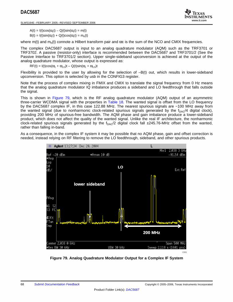
www.ti.com
C001
lower sideband
200 MHz
LO
lower sideband
200 MHz
LO
DAC5687
SLWS164E–FEBRUARY 2005–REVISED SEPTEMBER 2006
A(t) = I(t)cos(ωct) – Q(t)sin(ωct) = m(t)B(t) = I(t)sin(ωct) + Q(t)cos(ωct) = mh(t)
where m(t) and mh(t) connote a Hilbert transform pair and ωc is the sum of the NCO and CMIX frequencies.
The complex DAC5687 output is input to an analog quadrature modulator (AQM) such as the TRF3701 orTRF3702. A passive (resistor-only) interface is recommended between the DAC5687 and TRF3701/2 (See thePassive Interface to TRF3701/2 section). Upper single-sideband upconversion is achieved at the output of theanalog quadrature modulator, whose output is expressed as:
RF(t) = I(t)cos(ωc + ωLO)t – Q(t)sin(ωc + ωLO)t
Flexibility is provided to the user by allowing for the selection of –B(t) out, which results in lower-sidebandupconversion. This option is selected by usb in the CONFIG3 register.
Note that the process of complex mixing in FMIX and CMIX to translate the signal frequency from 0 Hz meansthat the analog quadrature modulator IQ imbalance produces a sideband and LO feedthrough that falls outsidethe signal.
This is shown in Figure 79, which is the RF analog quadrature modulator (AQM) output of an asymmetricthree-carrier WCDMA signal with the properties in Table 18. The wanted signal is offset from the LO frequencyby the DAC5687 complex IF, in this case 122.88 MHz. The nearest spurious signals are ~100 MHz away fromthe wanted signal (due to nonharmonic clock-related spurious signals generated by the fDAC/4 digital clock),providing 200 MHz of spurious-free bandwidth. The AQM phase and gain imbalance produce a lower-sidebandproduct, which does not affect the quality of the wanted signal. Unlike the real IF architecture, the nonharmonicclock-related spurious signals generated by the fDAC/2 digital clock fall ±245.76-MHz offset from the wanted,rather than falling in-band.
As a consequence, in the complex IF system it may be possible that no AQM phase, gain and offset correction isneeded, instead relying on RF filtering to remove the LO feedthrough, sideband, and other spurious products.
Figure 79. Analog Quadrature Modulator Output for a Complex IF System
68 Submit Documentation Feedback Copyright © 2005–2006, Texas Instruments Incorporated
Product Folder Link(s): DAC5687

www.ti.com
Application Example: Wide-Bandwidth Direct Baseband-to-RF Conversion
B0043-01
2DACI
Q
RFProcessing
TRF3750
DAC5687
2
22DAC
Phase/Gain/OffsetAdjust
TRF3701TRF3702TRF3703
GC1115and DPD
Processor
DAC5687
SLWS164E–FEBRUARY 2005–REVISED SEPTEMBER 2006
Table 18. Signal and System Properties for Complex IF System Example in Figure 79Signal Three WCDMA carriers, test model 1
Baseband carrier offsets –7.5 MHz, 2.5 MHz, 7.5 MHzDAC5687 input rate 122.88 MSPS
DAC5687 output rate 491.52 MSPS (4× interpolation)DAC5687 mode X4 CMIX
DAC5687 complex IF 122.88 MHz (fDAC/4)LO frequency 2140 MHz
The complex IF has several advantages over the real IF architecture such as:• Uncalibrated sideband suppression, ~35 dBc compared to 0 dBc for real IF architecture.• Direct DAC–complex-mixer connection—no amplifiers• Nonharmonic clock-related spurious signals fall out-of-band• DAC second Nyquist zone image is offset fDAC compared with fDAC – 2 × IF for a real IF architecture, reducing
the need for filtering at the DAC output.• Uncalibrated LO feedthrough for AQM is ~35 dBc and calibration can reduce or completely remove the LO
feedthrough.
A system example of the DAC5687 used in a wide-bandwidth direct baseband-to-RF conversion is shown inFigure 80. The DAC input would typically be generated by a crest factor reduction processor such as TexasInstruments GC1115 and digital predistortion processor. With a complex baseband input, the DAC5687 would beused to increase the data rate through interpolation. In addition, phase, gain, and offset correction of the IQimbalance is possible using the QMC block, DAC gain, and DAC offset features. The correction could be doneone time during manufacturing (see the TRF3701 data sheet (SLWS145) and the TRF3702 data sheet(SLWS149) for the variation with temperature, supply, LO frequency, etc., after calibration at nominal conditions)or during operation with a separate feedback loop measuring imbalance in the RF signal.
Figure 80. Direct Conversion System Using DAC5687 in X4L Mode
Operating at baseband has the advantage that the DAC5687 output is insensitive to DAC sample clock phasenoise, so using the DAC PLL clock mode has similar spectral performance to the external clock mode. Inaddition, the nonharmonic clock-related spurious signals are small due to the low DAC output frequency.
With a complex input rate specified up to 250 MSPS, the DAC5687 is capable of producing signals with up to200-MHz bandwidth for systems such as digital predistortion (DPD).
Copyright © 2005–2006, Texas Instruments Incorporated Submit Documentation Feedback 69
Product Folder Link(s): DAC5687

www.ti.com
Application Example: CMTS/VOD Transmitter
B0044-01
2DACCh2
Ch1
GC5016
DUCDAC5687
CDC7005
2
DUC
DUC
DUC
DAC
QAM1
QAM2
QAM3
QAM4
DAC5687
SLWS164E–FEBRUARY 2005–REVISED SEPTEMBER 2006
The exceptional SNR of the DAC5687 enables a dual-cable modem termination system (CMTS) or video ondemand (VOD) QAM transmitter in excess of the stringent DOCSIS specification, with > 74 dBc and 75 dBc inthe adjacent and alternate channels.
A typical system using the DAC5687 for a cost-optimized dual-channel two-QAM transmitter is shown inFigure 81. A GC5016 would take four separate symbol rate inputs and provide pulse shaping and interpolation to~128 MSPS. The four QAM carriers would be combined into two groups of two QAM carriers with intermediatefrequencies of approximately 30 MHz to 40 MHz. The GC5016 would output two real data streams to oneDAC5687. The DAC5687 would function as a dual-channel device and provide 2× interpolation to increase thefrequency of the second Nyquist zone image. The two signals are then output through the two DAC outputs,through a transformer and to an RF upconverter.
Figure 81. Dual-Channel Two-QAM CMTS Transmitter System Using DAC5687
The DAC5687 output for a two-QAM256 carrier signal at 33-MHz and 39-MHz IF with the signal and systemproperties listed in Table 19 is shown in Figure 82. The low DAC5687 noise floor provides better than 75 dBc(equal bandwidth normalized to one QAM256 power) at > 6-MHz offset.
Table 19. Signal and System Properties for Complex IF System Example in Figure 82Signal QAM256, 5.36 MSPS, α = 0.12
IF frequencies 33 MHz and 39 MHzDAC5687 input rate 5.36 MSPS × 24 = 128.64 MSPS
DAC5687 output rate 257.28 MSPS (2× interpolation)DAC5687 mode X2
70 Submit Documentation Feedback Copyright © 2005–2006, Texas Instruments Incorporated
Product Folder Link(s): DAC5687

www.ti.com
C002
Application Example: High-Speed Arbitrary Waveform Generator
B0045-01
DAC
Odd
Even
InputMultiplexer
DigitalPattern
Generator
DAC5687
DAC5687
SLWS164E–FEBRUARY 2005–REVISED SEPTEMBER 2006
Figure 82. Two QAM256 Carriers With 36-MHz IF
The DAC5687 flexible input allows use of the dual input ports with demultiplexed odd/even samples at acombined rate of up to 500 MSPS. Combined with the DAC 16-bit resolution, the DAC5687 allows widebandsignal generation for test and measurement applications.
Figure 83. DAC5687 in Odd/Even Input Mode
Copyright © 2005–2006, Texas Instruments Incorporated Submit Documentation Feedback 71
Product Folder Link(s): DAC5687
www.ti.com
DAC5687
SLWS164E–FEBRUARY 2005–REVISED SEPTEMBER 2006
Changes from Revision D (July 2006) to Revision E ...................................................................................................... Page
• Inverted CLK2 waveform in Figure 50 timing diagram ....................................................................................................... 44• Deleted Δ < talign from Figure 51 timing diagram.................................................................................................................. 44
Changes from Revision C (April 2006) to Revision D .................................................................................................... Page
• For pins 34 and 92 in pinout diagram, changed "MSB" to "MSB or LSB," and for pins 55 and 71 changed "LSB" to"LSB or MSB," to reflect option of bus reversal. .................................................................................................................... 3
• Added VIH and VIL specifications for IOVDD = 1.8 V ............................................................................................................. 9• In register CONFIG3, added sentence to counter_mode(2:0) description indicating that counter mode replaces
digital signal with a counter signal ....................................................................................................................................... 27• In register NCO_FREQ_2, changed address to 0x0B......................................................................................................... 28• In register NCO_FREQ_3, changed address to 0x0C......................................................................................................... 28• In register DACA_DACB_GAIN_1, added daca_gain(11:8) to description ......................................................................... 30• In the description of instruction bytes N1 and N0, added description of multibyte transfers............................................... 32• For FIR filters, corrected description (color and type) of lines in Figure 38......................................................................... 34• Changed "... FMIX + fDAC/2" to "FMIX + CMIX with fDAC/2" ................................................................................................. 36• Changed fDAC to fNCO in Figure 39........................................................................................................................................ 36• To DAC Offset Control section, appended description of the transition between offset values during four DAC clock
cycles (two paragraphs and Table 11)................................................................................................................................. 39• Added sentence in external clock mode description explaining that the PLLLOCK output should not be used above
100 MHz for IOVDD = 1.8 V ................................................................................................................................................ 41• In dual clock mode equation, changed "falign" to "talign"......................................................................................................... 43• Appended paragraph to Interleave Bus Mode section describing issues with synchronization in PLL mode with
interleaved data ................................................................................................................................................................... 45• First sentence of Input FIFO section, changed "DAC clock mode" to "external clock mode" ............................................. 45• Changed second "=" in equation to a "–"............................................................................................................................. 52• Changed "The external output resistors are referred to an external ground." to "The external output resistors are
referred to AVDD." .............................................................................................................................................................. 52• Changed "Exceeding the output compliance voltage..." to "Exceeding the minimum output compliance voltage...".......... 52• Changed "does not exceed 0.5 V" to "is in the range of AVDD ±0.5 V."............................................................................. 52• Appended sentence, "The pullup and pulldown circuitry is approximately equivalent to 100 kΩ." ..................................... 55• Changed caption of Figure 65 ............................................................................................................................................. 56• Changed "...it is suggested that ωd be set... to "...it is suggested that φd be set..." ............................................................. 57• In last sentence of paragraph, changed "1.56-VPP differential" to "1.52-VPP differential" ................................................... 58• Changed example of an interface to a 1.5-V common-mode device to an interface to a 3.3-V common mode for
TRF3703-33......................................................................................................................................................................... 59• In Table 16, changed value in top row of Frequency/fDAC column from 0.7 to 0.07 ........................................................... 64• In text for example #2, changed "...fDAC/2 and fDAC/4 signal is adjusted..." to "...fDAC/2 spurious signal is adjusted..." ...... 65• Changed referenced figure number to Figure 82 ................................................................................................................ 70
72 Submit Documentation Feedback Copyright © 2005–2006, Texas Instruments Incorporated
Product Folder Link(s): DAC5687
www.ti.com
DAC5687
SLWS164E–FEBRUARY 2005–REVISED SEPTEMBER 2006
Changes from Revision B (June 2005) to Revision C .................................................................................................... Page
• First sentence: Changed "The lower limit" to "upper limit". 3rd sentence: "upper limit" to "lower limit". Last sentence:"Exceeding the upper limit" to "Exceeding the limits". ........................................................................................................... 6
• Noise Floor Test Conditions: Swapped "CLK1 = 122.88 MHz" and "CLK2 = 491.52 MHz" for all four lines........................ 9• Input data rate, External or dual-clock modes, minimum changed to 0 Hz........................................................................... 9• Input data rate, PLL clock mode, minimum changed to 2.5 MHz.......................................................................................... 9• VCO maximum frequency test condition, "pll_kv = 0" changed to "pll_kv = 1" and vice versa........................................... 10• VCO minimum frequency test condition, "pll_kv = 0" changed to "pll_kv = 1" and vice versa............................................ 10• Figure 26 – "16702A Pattern Generator Card" changed to "16720A Pattern Generator Card" .......................................... 18• Figure 27 – "16702A Pattern Generator Card" changed to "16720A Pattern Generator Card" .......................................... 19• Figure 45: changed "CLK2" to "CLK1"................................................................................................................................. 42• Second paragraph of Analog Current Outputs reworded .................................................................................................... 52• Table 15: "pll_kv = 0" changed to "pll_kv = 1" and vice versa ............................................................................................ 57• Figure 72 caption – changed "X4 and X4L" to "X8" ............................................................................................................ 61• Figure 81 – removed one stage of interpolation from DAC block diagram ......................................................................... 70
Changes from Revision A (April 2005) to Revision B .................................................................................................... Page
• Added thermal pad dimensions ............................................................................................................................................. 1• Reversed "External Clock Mode" and "PLL Clock Mode" in noise floor test ......................................................................... 9• Changed PLLLOCK Output Signal for PLLVDD = 0 to "Normal Operation" in Table 5 ...................................................... 31• Reversed ts(DATA) and th(DATA) in Figure 43............................................................................................................................ 41• Reversed ts(DATA) and th(DATA) in Figure 44............................................................................................................................ 41• Reversed ts(DATA) and th(DATA) in Figure 45............................................................................................................................ 42• Updated Figure 46 ............................................................................................................................................................... 42
Copyright © 2005–2006, Texas Instruments Incorporated Submit Documentation Feedback 73
Product Folder Link(s): DAC5687

PACKAGE OPTION ADDENDUM
www.ti.com 10-Jun-2014
Addendum-Page 1
PACKAGING INFORMATION
Orderable Device Status(1)
Package Type PackageDrawing
Pins PackageQty
Eco Plan(2)
Lead/Ball Finish(6)
MSL Peak Temp(3)
Op Temp (°C) Device Marking(4/5)
Samples
DAC5687IPZP ACTIVE HTQFP PZP 100 90 Green (RoHS& no Sb/Br)
CU NIPDAU Level-3-260C-168 HR -40 to 85 DAC5687IPZP
DAC5687IPZPG4 ACTIVE HTQFP PZP 100 90 Green (RoHS& no Sb/Br)
CU NIPDAU Level-3-260C-168 HR -40 to 85 DAC5687IPZP
DAC5687IPZPR ACTIVE HTQFP PZP 100 1000 Green (RoHS& no Sb/Br)
CU NIPDAU Level-3-260C-168 HR -40 to 85 DAC5687IPZP
(1) The marketing status values are defined as follows:ACTIVE: Product device recommended for new designs.LIFEBUY: TI has announced that the device will be discontinued, and a lifetime-buy period is in effect.NRND: Not recommended for new designs. Device is in production to support existing customers, but TI does not recommend using this part in a new design.PREVIEW: Device has been announced but is not in production. Samples may or may not be available.OBSOLETE: TI has discontinued the production of the device.
(2) Eco Plan - The planned eco-friendly classification: Pb-Free (RoHS), Pb-Free (RoHS Exempt), or Green (RoHS & no Sb/Br) - please check http://www.ti.com/productcontent for the latest availabilityinformation and additional product content details.TBD: The Pb-Free/Green conversion plan has not been defined.Pb-Free (RoHS): TI's terms "Lead-Free" or "Pb-Free" mean semiconductor products that are compatible with the current RoHS requirements for all 6 substances, including the requirement thatlead not exceed 0.1% by weight in homogeneous materials. Where designed to be soldered at high temperatures, TI Pb-Free products are suitable for use in specified lead-free processes.Pb-Free (RoHS Exempt): This component has a RoHS exemption for either 1) lead-based flip-chip solder bumps used between the die and package, or 2) lead-based die adhesive used betweenthe die and leadframe. The component is otherwise considered Pb-Free (RoHS compatible) as defined above.Green (RoHS & no Sb/Br): TI defines "Green" to mean Pb-Free (RoHS compatible), and free of Bromine (Br) and Antimony (Sb) based flame retardants (Br or Sb do not exceed 0.1% by weightin homogeneous material)
(3) MSL, Peak Temp. - The Moisture Sensitivity Level rating according to the JEDEC industry standard classifications, and peak solder temperature.
(4) There may be additional marking, which relates to the logo, the lot trace code information, or the environmental category on the device.
(5) Multiple Device Markings will be inside parentheses. Only one Device Marking contained in parentheses and separated by a "~" will appear on a device. If a line is indented then it is a continuationof the previous line and the two combined represent the entire Device Marking for that device.
(6) Lead/Ball Finish - Orderable Devices may have multiple material finish options. Finish options are separated by a vertical ruled line. Lead/Ball Finish values may wrap to two lines if the finishvalue exceeds the maximum column width.
Important Information and Disclaimer:The information provided on this page represents TI's knowledge and belief as of the date that it is provided. TI bases its knowledge and belief on informationprovided by third parties, and makes no representation or warranty as to the accuracy of such information. Efforts are underway to better integrate information from third parties. TI has taken and

PACKAGE OPTION ADDENDUM
www.ti.com 10-Jun-2014
Addendum-Page 2
continues to take reasonable steps to provide representative and accurate information but may not have conducted destructive testing or chemical analysis on incoming materials and chemicals.TI and TI suppliers consider certain information to be proprietary, and thus CAS numbers and other limited information may not be available for release.
In no event shall TI's liability arising out of such information exceed the total purchase price of the TI part(s) at issue in this document sold by TI to Customer on an annual basis.
OTHER QUALIFIED VERSIONS OF DAC5687 :
• Enhanced Product: DAC5687-EP
NOTE: Qualified Version Definitions:
• Enhanced Product - Supports Defense, Aerospace and Medical Applications
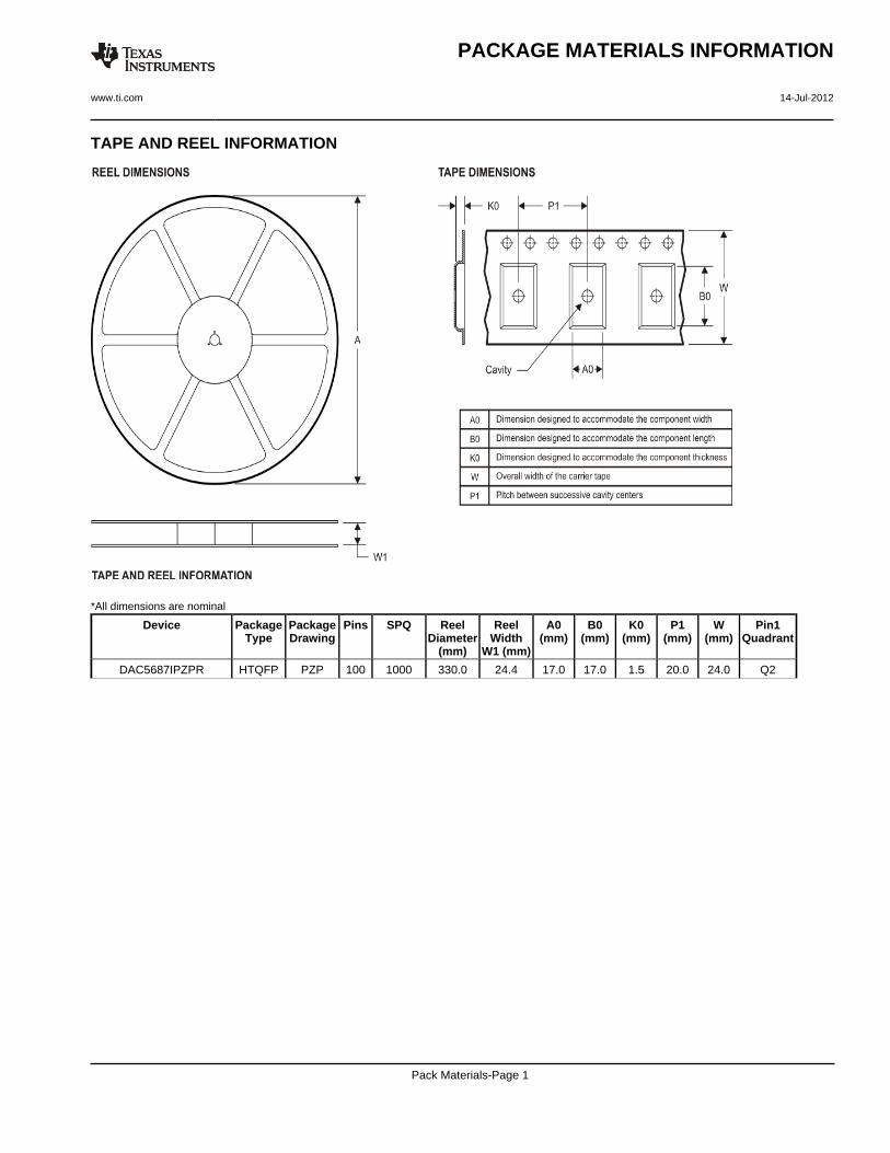
TAPE AND REEL INFORMATION
*All dimensions are nominal
Device PackageType
PackageDrawing
Pins SPQ ReelDiameter
(mm)
ReelWidth
W1 (mm)
A0(mm)
B0(mm)
K0(mm)
P1(mm)
W(mm)
Pin1Quadrant
DAC5687IPZPR HTQFP PZP 100 1000 330.0 24.4 17.0 17.0 1.5 20.0 24.0 Q2
PACKAGE MATERIALS INFORMATION
www.ti.com 14-Jul-2012
Pack Materials-Page 1

*All dimensions are nominal
Device Package Type Package Drawing Pins SPQ Length (mm) Width (mm) Height (mm)
DAC5687IPZPR HTQFP PZP 100 1000 367.0 367.0 45.0
PACKAGE MATERIALS INFORMATION
www.ti.com 14-Jul-2012
Pack Materials-Page 2

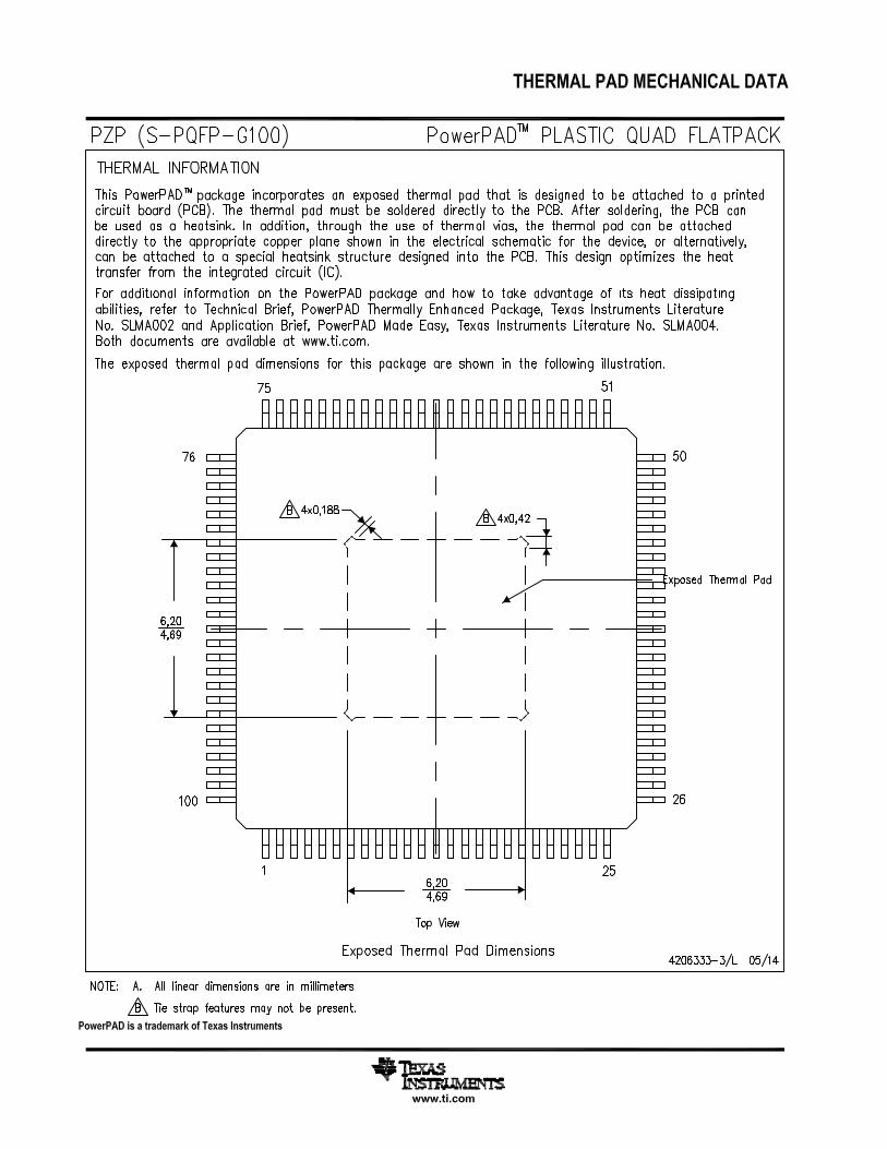

IMPORTANT NOTICETexas Instruments Incorporated and its subsidiaries (TI) reserve the right to make corrections, enhancements, improvements and otherchanges to its semiconductor products and services per JESD46, latest issue, and to discontinue any product or service per JESD48, latestissue. Buyers should obtain the latest relevant information before placing orders and should verify that such information is current andcomplete. All semiconductor products (also referred to herein as “components”) are sold subject to TI’s terms and conditions of salesupplied at the time of order acknowledgment.TI warrants performance of its components to the specifications applicable at the time of sale, in accordance with the warranty in TI’s termsand conditions of sale of semiconductor products. Testing and other quality control techniques are used to the extent TI deems necessaryto support this warranty. Except where mandated by applicable law, testing of all parameters of each component is not necessarilyperformed.TI assumes no liability for applications assistance or the design of Buyers’ products. Buyers are responsible for their products andapplications using TI components. To minimize the risks associated with Buyers’ products and applications, Buyers should provideadequate design and operating safeguards.TI does not warrant or represent that any license, either express or implied, is granted under any patent right, copyright, mask work right, orother intellectual property right relating to any combination, machine, or process in which TI components or services are used. Informationpublished by TI regarding third-party products or services does not constitute a license to use such products or services or a warranty orendorsement thereof. Use of such information may require a license from a third party under the patents or other intellectual property of thethird party, or a license from TI under the patents or other intellectual property of TI.Reproduction of significant portions of TI information in TI data books or data sheets is permissible only if reproduction is without alterationand is accompanied by all associated warranties, conditions, limitations, and notices. TI is not responsible or liable for such altereddocumentation. Information of third parties may be subject to additional restrictions.Resale of TI components or services with statements different from or beyond the parameters stated by TI for that component or servicevoids all express and any implied warranties for the associated TI component or service and is an unfair and deceptive business practice.TI is not responsible or liable for any such statements.Buyer acknowledges and agrees that it is solely responsible for compliance with all legal, regulatory and safety-related requirementsconcerning its products, and any use of TI components in its applications, notwithstanding any applications-related information or supportthat may be provided by TI. Buyer represents and agrees that it has all the necessary expertise to create and implement safeguards whichanticipate dangerous consequences of failures, monitor failures and their consequences, lessen the likelihood of failures that might causeharm and take appropriate remedial actions. Buyer will fully indemnify TI and its representatives against any damages arising out of the useof any TI components in safety-critical applications.In some cases, TI components may be promoted specifically to facilitate safety-related applications. With such components, TI’s goal is tohelp enable customers to design and create their own end-product solutions that meet applicable functional safety standards andrequirements. Nonetheless, such components are subject to these terms.No TI components are authorized for use in FDA Class III (or similar life-critical medical equipment) unless authorized officers of the partieshave executed a special agreement specifically governing such use.Only those TI components which TI has specifically designated as military grade or “enhanced plastic” are designed and intended for use inmilitary/aerospace applications or environments. Buyer acknowledges and agrees that any military or aerospace use of TI componentswhich have not been so designated is solely at the Buyer's risk, and that Buyer is solely responsible for compliance with all legal andregulatory requirements in connection with such use.TI has specifically designated certain components as meeting ISO/TS16949 requirements, mainly for automotive use. In any case of use ofnon-designated products, TI will not be responsible for any failure to meet ISO/TS16949.Products ApplicationsAudio www.ti.com/audio Automotive and Transportation www.ti.com/automotiveAmplifiers amplifier.ti.com Communications and Telecom www.ti.com/communicationsData Converters dataconverter.ti.com Computers and Peripherals www.ti.com/computersDLP® Products www.dlp.com Consumer Electronics www.ti.com/consumer-appsDSP dsp.ti.com Energy and Lighting www.ti.com/energyClocks and Timers www.ti.com/clocks Industrial www.ti.com/industrialInterface interface.ti.com Medical www.ti.com/medicalLogic logic.ti.com Security www.ti.com/securityPower Mgmt power.ti.com Space, Avionics and Defense www.ti.com/space-avionics-defenseMicrocontrollers microcontroller.ti.com Video and Imaging www.ti.com/videoRFID www.ti-rfid.comOMAP Applications Processors www.ti.com/omap TI E2E Community e2e.ti.comWireless Connectivity www.ti.com/wirelessconnectivity
Mailing Address: Texas Instruments, Post Office Box 655303, Dallas, Texas 75265Copyright © 2014, Texas Instruments Incorporated