interpreting ideality factors for planar perovskite solar
TRANSCRIPT

PHYSICAL REVIEW APPLIED 14, 024031 (2020)
Interpreting Ideality Factors for Planar Perovskite Solar Cells: Ectypal DiodeTheory for Steady-State Operation
N.E. Courtier *
Mathematical Sciences, University of Southampton, Southampton, United Kingdom
(Received 10 March 2020; revised 20 May 2020; accepted 10 July 2020; published 12 August 2020)
Ideality factors are used to identify the dominant form of recombination in many types of solar cells andguide future development. Unusual noninteger and voltage-dependent ideality factors, which are difficultto explain using the classical diode theory, have been reported for perovskite solar cells and remain unex-plained. Experimental measurements and theoretical simulations of the electric potential profile acrossa planar perovskite solar cell show that significant potential drops occur across each of the perovskite-and transport-layer interfaces. Such potential profiles are fundamentally distinct from the single potentialdrop that characterizes a p-n or a p-i-n junction. We propose an analytical model, developed specificallyfor perovskite devices, in which the ideality factor is replaced by a systematically derived analog, whichwe term the ectypal factor. In common with the classical theory, the ectypal diode equation is derivedas an approximation to a drift-diffusion model for the motion of charges across a solar cell, however,crucially, it incorporates the effects of ion migration within the perovskite absorber layer. The theory pro-vides a framework for analyzing the steady-state performance of a perovskite solar cell (PSC) accordingto the value of the ectypal factor. Predictions are verified against numerical simulations of a full set ofdrift-diffusion equations. An important conclusion is that our ability to evaluate PSC performance, usingstandard techniques such as the analysis of dark J -V or Suns-VOC measurements, relies on understandinghow the potential distribution varies with applied voltage. Implications of this work on the interpretationof data from the literature are discussed.
DOI: 10.1103/PhysRevApplied.14.024031
I. INTRODUCTION
The Shockley diode equation is commonly employed insolar-cell research to diagnose the recombination mech-anism that limits the performance of a particular devicearchitecture [1]. The diode model is derived from the the-ory of drift and diffusion of charge carriers across a solarcell, including the generation and recombination of chargecarrier pairs (electrons and holes). Though approximate,this model provides a useful description of the current-voltage (J -V) characteristics of many types of solar cell.The value of the diode ideality factor is key for the diag-nosis of both the type of recombination that limits cellperformance and its location within the device. It is there-fore crucial to be able to correctly evaluate and interpret thevalue of the ideality factor. However, in the case of metalhalide perovskite solar cells (PSCs), this approach has led
Published by the American Physical Society under the terms ofthe Creative Commons Attribution 4.0 International license. Fur-ther distribution of this work must maintain attribution to theauthor(s) and the published article’s title, journal citation, andDOI.
to some unexpected results, which cast doubt on its valid-ity in assessing this promising photovoltaic technology[2–6]. Perovskite solar cells have recorded a rapid rise inpower conversion efficiency over a short but intense periodof research effort [7,8]. However, the cells currently lacklong-term stability [9]. Success in the economic market(most likely via their incorporation into tandem deviceswith silicon [10,11]) will depend on our understandingof the fundamental physical mechanisms that control thebehavior of PSCs.
Experimental studies have reported ideality factors forPSCs ranging from 0.9 [12] to higher than 5 [2]. Such val-ues lie outside the typical range of values (1–2) predictedand explained by the theory behind the classical Shock-ley diode equation. Many noninteger values, for example,between 1 and 2, have also been reported [13–17], butare difficult to explain using the classical theory. A sum-mary of common and uncommon interpretations is givenin Ref. [3]. In the field of dye solar cells, noninteger ide-ality factors have been explained by the existence of abroad distribution of trap states combined with trap-limitedrecombination [18,19]. Noninteger ideality factors, includ-ing values smaller than 1, can also occur as a result ofenergetic misalignment between the absorber and contactmaterials [20–22].
2331-7019/20/14(2)/024031(21) 024031-1 Published by the American Physical Society

N.E. COURTIER PHYS. REV. APPLIED 14, 024031 (2020)
In both of the experimental studies mentioned above[2,12], the values of the ideality factor are calculatedfrom measurements of the open-circuit voltage (VOC) ofa PSC under different illumination intensities. This is oftenreferred to as the Suns-VOC method. Interestingly, Pockettet al. [2] report that the ideality factors for a set of 12 pla-nar PSCs, prepared at the same time, cluster around twodistinct values (approximately 2.6 and 5.2). Tress et al.[6] use three different experimental techniques to calcu-late the ideality factor for four types of PSC. The value ofthe ideality factor is shown to vary substantially dependingon how it is measured. Values calculated from the deriva-tive of a J -V curve measured in the dark, referred to asthe dark J -V method, are shown to strongly depend on theapplied voltage. Tress et al. [6] conclude that the Suns-VOC method provides the most reliable values, while theambiguity in the dark J -V results is attributed to voltage-dependent parasitic resistances, although the exact originsare not known. Contreras-Bernal et al. [15,23] use analternative method in which the ideality factor is calcu-lated from the high-frequency impedance response of aPSC measured at open-circuit under different illumina-tion intensities. Voltage-dependent ideality factors are alsopublished in Ref. [24,25] and the Supplemental Materialof Ref. [3]. These recent findings highlight the need for aclear picture of the principle working mechanism of a PSC,which can be used to interpret and explain the unusual ide-ality factors of PSCs. This picture can be obtained froma detailed drift-diffusion model for a PSC based on themicroscopic properties of the device.
Combined experimental and theoretical studies, whichseek to understand the performance limitations of state-of-the-art PSCs, such as Refs. [3,4,16], conclude that currenttechniques for analysis do not provide reliable conclusions.Almora et al. [3] and Calado et al. [4] attribute the diffi-culty in determining a unique value for the ideality factorto the interference of undesirable hysteresis often observedin J -V measurements [26–29]. The origin of this J -V hys-teresis is most commonly attributed to the migration ofmobile ionic charge within the perovskite material. Recentreviews that discuss the impact of ion migration on thefuture prospects of PSCs are given in Ref. [30,31]. Thepresence of mobile ionic charge in PSCs means that use ofthe classical diode theory to analyze their behavior is notphysically justified and therefore traditional interpretationsof the ideality factor can be misleading.
Using the hypothesis that ion migration is the originof J -V hysteresis, Calado et al. [4] explain that it is theevolving profile of the electric potential across a PSC thathampers the measurement of a cell’s VOC, and thus theideality factor, by conventional means. It is noted thatthe interpretation of a steady-state ideality factor shouldtake into account the homogeneity of charge-carrier den-sities across the perovskite layer. An alternative methodfor the determination and interpretation of a “transient
ideality factor” is suggested, that involves comparing time-dependent measurements to the results of drift-diffusionsimulations. However, the suggested method depends onpreconditioning the cell in a particular initial state anddetermining the cell’s characteristics from a transient mea-surement, rather than from the steady-state conditions atwhich a cell is expected to operate.
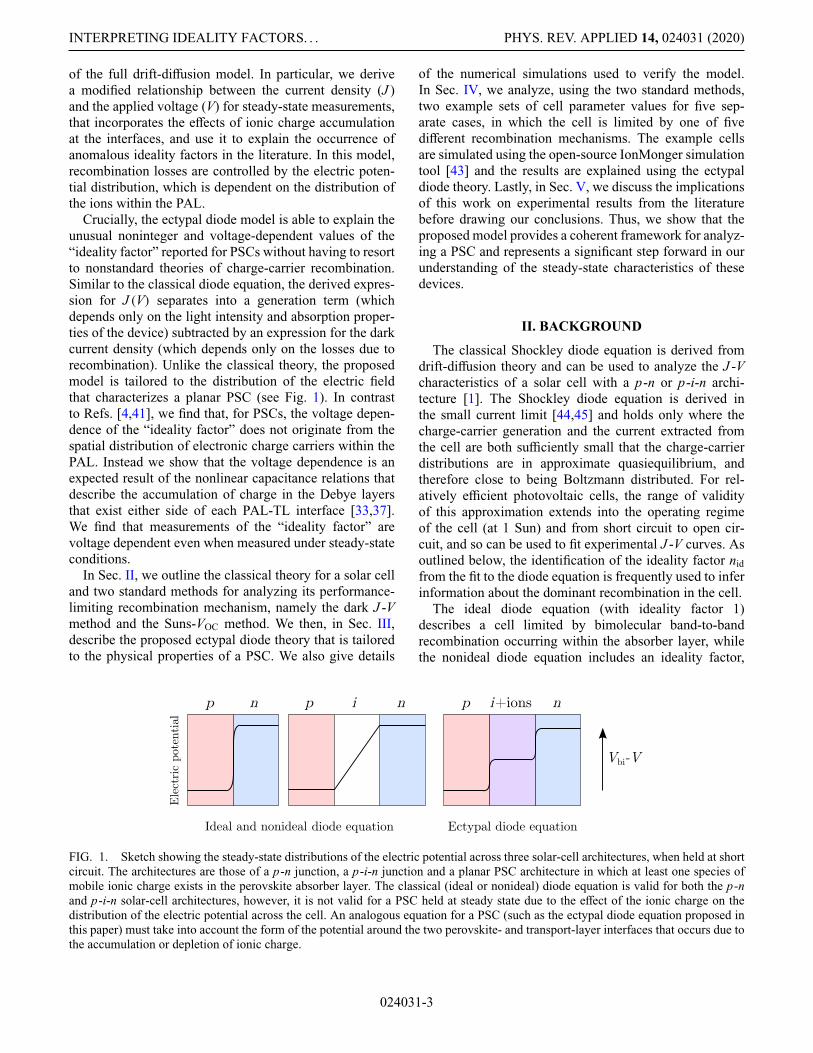
Drift-diffusion models incorporating mobile ioniccharge have been shown to be capable of reproducing awide variety of experimentally observed behavior [32–35].In PSCs, a high density of mobile ionic charge is predictedto exist within the perovskite material [36]. As a result, thedistribution of the electric field is controlled by the positionof the mobile ions and evolves on a slower timescale thanthat of the charge-carrier dynamics [4,33,37]. At steadystate, ionic accumulation or depletion at the edges of theperovskite absorber layer (PAL) screens the electric fieldfrom the bulk of the PAL and causes potential drops toform across the interfaces between the PAL and each ofthe transport layers (TLs). As such, the existence of mobileionic charge in a PSC produces a notably different potentialprofile from that of either a p-n or p-i-n junction, as shownin Fig. 1. The electric potential across the three core lay-ers of a PSC displays a linear profile across the bulk ofeach layer and rapid changes across narrow regions, calledDebye layers, immediately either side of each interface.Such profiles have been measured experimentally usingKelvin probe force microscopy (KPFM) and presented inRef. [38–40]. The proportion of the total potential differ-ence that falls across each Debye layer depends on therelative values of the permittivity and the mean density ofthe majority mobile charge species of each material layer[33].
The formation of potential drops due to charge accumu-lation at the absorber interfaces has also been found to besignificant in the study of thin-film silicon solar cells [41];although in such cells, the charge accumulation is of anelectronic nature and only screens a small proportion ofthe total potential drop. The model for a p-i-n solar cellpresented by Taretto [41] predicts voltage-dependent ideal-ity factors due to charge accumulation within the intrinsicabsorber layer and shows improved agreement with exper-imental data compared to classical diode theory. As such,Taretto [41] demonstrates how analytical modeling canbe used as a practical tool to elucidate the effects of keymaterial properties on the performance of a solar cell.
In this work, we develop a simple analytical modelappropriate for planar PSCs, which we term the ectypal[42] diode theory. This model describes the principle work-ing mechanism of a planar PSC operating in steady-stateconditions and can be used to quantitatively assess cellperformance in an analogous way to the classical diodetheory. The proposed model is systematically derived froma drift-diffusion model for ion migration and charge trans-port across a PSC and validated against numerical solution
024031-2
INTERPRETING IDEALITY FACTORS. . . PHYS. REV. APPLIED 14, 024031 (2020)
of the full drift-diffusion model. In particular, we derivea modified relationship between the current density (J )and the applied voltage (V) for steady-state measurements,that incorporates the effects of ionic charge accumulationat the interfaces, and use it to explain the occurrence ofanomalous ideality factors in the literature. In this model,recombination losses are controlled by the electric poten-tial distribution, which is dependent on the distribution ofthe ions within the PAL.
Crucially, the ectypal diode model is able to explain theunusual noninteger and voltage-dependent values of the“ideality factor” reported for PSCs without having to resortto nonstandard theories of charge-carrier recombination.Similar to the classical diode equation, the derived expres-sion for J (V) separates into a generation term (whichdepends only on the light intensity and absorption proper-ties of the device) subtracted by an expression for the darkcurrent density (which depends only on the losses due torecombination). Unlike the classical theory, the proposedmodel is tailored to the distribution of the electric fieldthat characterizes a planar PSC (see Fig. 1). In contrastto Refs. [4,41], we find that, for PSCs, the voltage depen-dence of the “ideality factor” does not originate from thespatial distribution of electronic charge carriers within thePAL. Instead we show that the voltage dependence is anexpected result of the nonlinear capacitance relations thatdescribe the accumulation of charge in the Debye layersthat exist either side of each PAL-TL interface [33,37].We find that measurements of the “ideality factor” arevoltage dependent even when measured under steady-stateconditions.
In Sec. II, we outline the classical theory for a solar celland two standard methods for analyzing its performance-limiting recombination mechanism, namely the dark J -Vmethod and the Suns-VOC method. We then, in Sec. III,describe the proposed ectypal diode theory that is tailoredto the physical properties of a PSC. We also give details
of the numerical simulations used to verify the model.In Sec. IV, we analyze, using the two standard methods,two example sets of cell parameter values for five sep-arate cases, in which the cell is limited by one of fivedifferent recombination mechanisms. The example cellsare simulated using the open-source IonMonger simulationtool [43] and the results are explained using the ectypaldiode theory. Lastly, in Sec. V, we discuss the implicationsof this work on experimental results from the literaturebefore drawing our conclusions. Thus, we show that theproposed model provides a coherent framework for analyz-ing a PSC and represents a significant step forward in ourunderstanding of the steady-state characteristics of thesedevices.
II. BACKGROUND
The classical Shockley diode equation is derived fromdrift-diffusion theory and can be used to analyze the J -Vcharacteristics of a solar cell with a p-n or p-i-n archi-tecture [1]. The Shockley diode equation is derived inthe small current limit [44,45] and holds only where thecharge-carrier generation and the current extracted fromthe cell are both sufficiently small that the charge-carrierdistributions are in approximate quasiequilibrium, andtherefore close to being Boltzmann distributed. For rel-atively efficient photovoltaic cells, the range of validityof this approximation extends into the operating regimeof the cell (at 1 Sun) and from short circuit to open cir-cuit, and so can be used to fit experimental J -V curves. Asoutlined below, the identification of the ideality factor nidfrom the fit to the diode equation is frequently used to inferinformation about the dominant recombination in the cell.
The ideal diode equation (with ideality factor 1)describes a cell limited by bimolecular band-to-bandrecombination occurring within the absorber layer, whilethe nonideal diode equation includes an ideality factor,
FIG. 1. Sketch showing the steady-state distributions of the electric potential across three solar-cell architectures, when held at shortcircuit. The architectures are those of a p-n junction, a p-i-n junction and a planar PSC architecture in which at least one species ofmobile ionic charge exists in the perovskite absorber layer. The classical (ideal or nonideal) diode equation is valid for both the p-nand p-i-n solar-cell architectures, however, it is not valid for a PSC held at steady state due to the effect of the ionic charge on thedistribution of the electric potential across the cell. An analogous equation for a PSC (such as the ectypal diode equation proposed inthis paper) must take into account the form of the potential around the two perovskite- and transport-layer interfaces that occurs due tothe accumulation or depletion of ionic charge.
024031-3

N.E. COURTIER PHYS. REV. APPLIED 14, 024031 (2020)
which extends the model to take into account lossesvia different recombination pathways. The nonideal diodeequation is given by
J (V) = Js − Jdark(V), (1a)
Jdark(V) = J0
[exp
(V
nidVT
)− 1
], (1b)
in which Js is the photogenerated current density (insidethe cell), Jdark is the dark current density (due to recom-bination), J0 is the saturation current density, nid is theideality factor, and VT = kBT/q is the thermal voltage.Here, kB is the Boltzmann constant, T is the temperature,and q is the elementary charge. In the ideal case of directradiative recombination, nid = 1. When other types of bulkrecombination dominate, the ideality factor is expected toequal nid = 2/γ where γ is the reaction order, i.e., nid =2 indicates first-order bulk recombination, nid = 1 indi-cates bimolecular bulk recombination and nid = 2
3 signifiestrimolecular Auger recombination [1,20,46]. A value ofnid = 2 is typically interpreted as trap-assisted Shockley-Read-Hall (SRH) recombination. Meanwhile, nid = 1 canalso be the result of dominant surface recombination.Other, less common, interpretations are summarized in theSupplemental Material of Ref. [3], such as recombinationdue to a nonuniform distribution of recombination centres.Calado et al. [4] provide multiple interpretations of ideal-ity factors equal to 1 or 2, which are due to either SRH orband-to-band recombination mechanisms.
In reality, the value of an ideality factor can vary withvoltage due to a change in the dominant form of recombi-nation. This scenario can be described using a two-diodemodel. However, the associated increase in the number offitting parameters means that this approach can yield erro-neous results. This approach is also not able to explainthe unusual values of the ideality factor that have beenreported for PSCs in the literature, in particular, those out-side of the range 1–2 and those that vary slowly withapplied voltage. The classical model can also be extendedby incorporating the effects of external series and shuntand parallel resistance into the classical diode equation[1]. However, fitting series and shunt resistance parame-ters to experimental data provides little information aboutthe location of recombination losses and also does notseem to explain the anomalous voltage-dependent valuesof the ideality factor reported for PSCs. So, in this work,we assume that just one recombination mechanism con-trols the observed behavior and that the losses due toexternal resistances are negligible for a high-efficiency celloperating in its power-generating regime.
The value of the ideality factor nid can be estimatedusing a number of different experimental procedures. Tresset al. [6] describe how nid may be calculated from fitting
(a) measurements of dark J -V curves, (b) open-circuit volt-age versus illumination intensity measurements (known asthe Suns-VOC method), and (c) electroluminescence mea-surements. The dark J -V method is also used in Refs.[24,25,40], while the Suns-VOC method is also used inRefs. [2,4,12,16,34]. We consider both the dark J -V andSuns-VOC methods in this work.
For positive applied voltages V � VT (usually taken tomean V � 0.1 V), the exponential term in the dark currentdensity in Eq. (1b) dominates so that the Shockley diodeequation can be approximated by
J (V) = Js − J0 exp(
VnidVT
). (2)
In the dark J -V method, the photogenerated current densityJs is zero and so the ideality factor is calculated from theslope of the logarithm of the dark current density from Eq.(2) versus applied voltage, via
nid = 1VT
(∂ ln Jdark
∂V
)−1
. (3)
Though the value of an ideality factor is expected to beapproximately constant, Wetzelaer et al. [24] show, usingthis method, that the value of the ideality factor for a planarPSC is strongly voltage dependent and varies with temper-ature. Other reports of strongly voltage-dependent idealityfactors for a variety of PSC architectures are given in Refs.[6,24,25].
The Suns-VOC method relies on the assumption thatthe photogenerated current density Js is proportional tothe illumination intensity and the dominant recombinationmechanism does not vary with illumination. In this case,measurements of the open-circuit voltage over a rangeof illumination intensities can be used to determine theideality factor via
nid = 1VT
∂VOC
∂ ln Fph, (4)
where Fph is the incident photon-flux density. The Suns-VOC method is deemed to be more reliable than the dark J -V method because measurements performed at open circuitare not affected by parasitic series resistance.
III. METHODS
A. Surface-polarization model
The fundamental difference between the classical modeland the surface-polarization model for a PSC lies in thedistribution of the electric field across a device, see Fig. 1.Both models are derived from drift-diffusion theory forthe transport of mobile charges in one dimension acrossa device. In the classical model for a p-n or p-i-n junction,
024031-4

INTERPRETING IDEALITY FACTORS. . . PHYS. REV. APPLIED 14, 024031 (2020)
there is one significant potential drop (or diode junction)within the device, which acts to separate the photogen-erated charge. However, across a planar PSC two majorpotential drops have been observed to exist, one at eachof the interfaces between the PAL and one of the transportlayers [38–40], as depicted in Fig. 2. Such a distribution isalso predicted by drift-diffusion simulations in which theelectric field across a PSC depends on the distribution ofa large density of mobile ionic charge, as well as the elec-tronic charge in the device. The distribution of the electricpotential is crucial for determining the performance of acell because current losses (due to recombination occur-ring either within the bulk or at the interfaces) depend onboth the potential energy that must be overcome for chargecarriers to recombine as well as the local charge-carrierconcentrations, which in turn also depend on the potential.Therefore, current losses strongly depend on the locationof potential drops within a cell.
Figure 2 shows the typical form of a steady-state poten-tial profile across the three core layers of a planar PSC.The total potential drop across the cell is entirely taken upwithin four narrow Debye layers either side of the PAL-TL interfaces. These potential drops are labeled V1−4. Thepotential is expected to take this form in a PSC that satis-fies the following assumptions of the surface-polarizationmodel [33] that: (i) a high density of mobile ionic chargeexists within the PAL, in comparison to the densities ofelectronic charge carriers that exist under illuminationintensities up to the equivalent of 1 Sun, (ii) the Debyelength associated with the majority species of mobilecharge in each material layer is much smaller than thewidth of that layer, and (iii) the timescale for equilibrationof the charge carriers in the TLs is much faster than that ofthe mobile ionic charge in the perovskite. For a mean ionvacancy density of 1.6 × 1025 m−3 in the PAL, the ionic
Debye length is on the order of a few nm. Such a shortDebye length means that the narrow Debye layers pre-dicted by the surface-polarization model may be difficultto resolve experimentally due to lower limits on the spatialresolution of KPFM of 20–30 nm [39]. However, there isgood agreement between the model and published KPFMdata that, rather than a single diode junction, there are sig-nificant potential drops across both PAL-TL interfaces in aPSC.
Previously, theoretical studies of surface-polarizationmodels have focused on explaining the origin of theproblematic J -V hysteresis exhibited by PSCs [33,37,47].Other unusual characteristics, which have been encoun-tered when using alternative characterization techniquesto assess PSCs, such as electrochemical impedance spec-troscopy (EIS) have also been studied [48]. In this work,we focus exclusively on the steady-state performance ofPSCs. Steady-state performance provides the most accu-rate assessment of the true potential of PSCs. Here, theterm steady state is used to describe measurements inwhich changes in applied voltage are sufficiently slow thatthe potential distribution is continuously in equilibriumwith the experimental conditions, i.e., the electric field inthe bulk of the PAL is completely screened by the potentialdrops V1−4 throughout the measurement.
The potential drops that lie within the perovskite (V2and V3 in Fig. 2) correspond to an accumulation of pre-dominantly ionic charge, while the potential drops in theelectron transport layer (ETL) and hole transport layer(HTL) (V1 and V4, respectively) correspond to an equal andopposite accumulation of electronic charge [33]. There-fore, the potential drops V1−4 obey different capacitancerelations for each Debye layer. The capacitance relationsderived in Ref. [33] are restated in Appendix A. Note thateven the two Debye layers that lie within the perovskite
FIG. 2. Sketch showing the steady-state potential distribution across a planar PSC, when held at short circuit, alongside a diagramof the five different recombination processes considered in this work. When an electric field exists across the bulk of the perovskiteabsorber layer, the mobile ionic charge that exists within the layer migrates until sufficient charge has accumulated adjacent to thePAL-TL interfaces to compensate the potential difference across the cell. Therefore, at steady state, the electric field within the bulk ofthe PAL is zero (i.e., the potential is flat) and the potential difference across the cell is taken up solely within the four potential drops(labeled V1−4) either side of each of the PAL-TL interfaces. For each of the recombination processes, the downwards-pointing bluearrow represents the potential energy to be overcome by an electron from the external circuit, while the upwards-pointing red arrowrepresents the same for a hole, in order for pair of charge carriers to recombine. The larger arrows indicate the processes, which limit,and therefore control, the rates of recombination.
024031-5
N.E. COURTIER PHYS. REV. APPLIED 14, 024031 (2020)
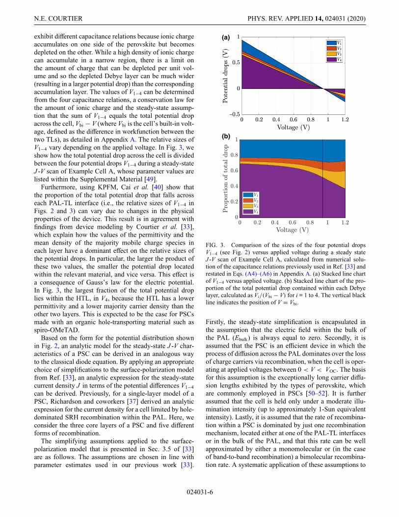
exhibit different capacitance relations because ionic chargeaccumulates on one side of the perovskite but becomesdepleted on the other. While a high density of ionic chargecan accumulate in a narrow region, there is a limit onthe amount of charge that can be depleted per unit vol-ume and so the depleted Debye layer can be much wider(resulting in a larger potential drop) than the correspondingaccumulation layer. The values of V1−4 can be determinedfrom the four capacitance relations, a conservation law forthe amount of ionic charge and the steady-state assump-tion that the sum of V1−4 equals the total potential dropacross the cell, Vbi − V (where Vbi is the cell’s built-in volt-age, defined as the difference in workfunction between thetwo TLs), as detailed in Appendix A. The relative sizes ofV1−4 vary depending on the applied voltage. In Fig. 3, weshow how the total potential drop across the cell is dividedbetween the four potential drops V1−4 during a steady-stateJ -V scan of Example Cell A, whose parameter values arelisted within the Supplemental Material [49].
Furthermore, using KPFM, Cai et al. [40] show thatthe proportion of the total potential drop that falls acrosseach PAL-TL interface (i.e., the relative sizes of V1−4 inFigs. 2 and 3) can vary due to changes in the physicalproperties of the device. This result is in agreement withfindings from device modeling by Courtier et al. [33],which explain how the values of the permittivity and themean density of the majority mobile charge species ineach layer have a dominant effect on the relative sizes ofthe potential drops. In particular, the larger the product ofthese two values, the smaller the potential drop locatedwithin the relevant material, and vice versa. This effect isa consequence of Gauss’s law for the electric potential.In Fig. 3, the largest fraction of the total potential droplies within the HTL, in V4, because the HTL has a lowerpermittivity and a lower majority carrier density than theother two layers. This is expected to be the case for PSCsmade with an organic hole-transporting material such asspiro-OMeTAD.
Based on the form for the potential distribution shownin Fig. 2, an analytic model for the steady-state J -V char-acteristics of a PSC can be derived in an analogous wayto the classical diode equation. By applying an appropriatechoice of simplifications to the surface-polarization modelfrom Ref. [33], an analytic expression for the steady-statecurrent density J in terms of the potential differences V1−4can be derived. Previously, for a single-layer model of aPSC, Richardson and coworkers [37] derived an analyticexpression for the current density for a cell limited by hole-dominated SRH recombination within the PAL. Here, weconsider the three core layers of a PSC and five differentforms of recombination.
The simplifying assumptions applied to the surface-polarization model that is presented in Sec. 3.5 of [33]are as follows. The assumptions are chosen in line withparameter estimates used in our previous work [33].
(a)
(b)
FIG. 3. Comparison of the sizes of the four potential dropsV1−4 (see Fig. 2) versus applied voltage during a steady stateJ -V scan of Example Cell A, calculated from numerical solu-tion of the capacitance relations previously used in Ref. [33] andrestated in Eqs. (A4)–(A6) in Appendix A. (a) Stacked line chartof V1−4 versus applied voltage. (b) Stacked line chart of the pro-portion of the total potential drop contained within each Debyelayer, calculated as Vi/(Vbi − V) for i = 1 to 4. The vertical blackline indicates the position of V = Vbi.
Firstly, the steady-state simplification is encapsulated inthe assumption that the electric field within the bulk ofthe PAL (Ebulk) is always equal to zero. Secondly, it isassumed that the PSC is an efficient device in which theprocess of diffusion across the PAL dominates over the lossof charge carriers via recombination, when the cell is oper-ating at applied voltages between 0 < V < VOC. The basisfor this assumption is the exceptionally long carrier diffu-sion lengths exhibited by the types of perovskite, whichare commonly employed in PSCs [50–52]. It is furtherassumed that the cell is held only under a moderate illu-mination intensity (up to approximately 1-Sun equivalentintensity). Lastly, it is assumed that the rate of recombina-tion within a PSC is dominated by just one recombinationmechanism, located either at one of the PAL-TL interfacesor in the bulk of the PAL, and that this rate can be wellapproximated by either a monomolecular or (in the caseof band-to-band recombination) a bimolecular recombina-tion rate. A systematic application of these assumptions to
024031-6

INTERPRETING IDEALITY FACTORS. . . PHYS. REV. APPLIED 14, 024031 (2020)
the equations that form the surface polarization model inRef. [33] is deferred to Appendix A. The simplificationsare verified against numerical simulations of a fully cou-pled charge-transport model. For details of the numericalmethod, see Sec. III B.
The result of systematically applying these assumptionsis the following equation for the current density, which weterm the ectypal diode equation for steady-state operation:
J (V) = Js − Jd exp(
V − Vbi
necVT
), nec = Vbi − V
F(V), (5)
where Js is the current density due to photogeneration, Jdis a constant of proportionality for the current density lostto recombination and, in analogy with the ideality factorfor the nonideal diode equation, we introduce nec as theectypal factor. This voltage-dependent, dimensionless fac-tor depends on the dominant pathway for recombinationtaking place within a device, via its dependence on thefunction F(V). The function F(V) captures the effect ofionic accumulation on the rate of recombination.
The value of Js depends only on the illumination inten-sity Is and light-absorption properties of the PAL, whilethe value of Jd depends only on material properties of thedevice, see Table V. The function F(V) depends only onthe voltage-dependent Debye layer potential drops V1−4,see Table I. In physical terms, F(V) equals the potentialdifference, which forms a potential barrier to the recombi-nation of charge carriers, at a given applied voltage. Theectypal factor nec is the reciprocal of the proportion of thetotal potential drop that forms a barrier to the dominantpathway for recombination, and is therefore expected totake positive values greater than 1. Five example cases arelisted in Table I. For details of how to evaluate the poten-tial drops V1−4 and hence calculate the current densityexpressed in Eq. (5), see Appendix 4.
Notably, Eq. (5) takes the same form as the approxi-mate Shockley diode equation for positive applied voltages(V � VT) stated in Eq. (2). However, Eq. (5) incorpo-rates an important modification in the form of the ectypalfactor, which relates the performance of a PSC to theperformance-limiting recombination mechanism and theinternal distribution of the electric potential resulting fromthe accumulation of ionic charge within the PAL.
In addition to the mathematical derivation presented inAppendix A, a simple intuitive explanation for the resultsin Table I is provided as follows. When a PSC is in oper-ation, current is generated by electrons entering the cellvia the anode (by extracting a hole), traveling through theHTL and into the perovskite where they can be excitedinto the conduction band via the absorption of light. Freeelectrons are then extracted through the ETL and the cath-ode to complete the circuit. Current is also lost due tocharge-carrier recombination within the cell. Note thatrecombination currents flow in the opposite direction to
the photogenerated current. The total current is, there-fore, the difference between the photogenerated currentand the recombination current. The amount of recombina-tion depends on the number of available charge carriersand the likelihood of recombination via a particular path-way. In the case of radiative recombination within thePAL, the rate of recombination takes a bimolecular form(R ≈ βnp) as it depends on the availability of both a freeelectron and a hole. Therefore, the potential energy bar-rier to recombination F(V) is equal to the total potentialdrop across the cell and so nec = 1. Note that this result isequivalent to the ideal case in the classical diode theory.In contrast, nonradiative recombination mechanisms (e.g.,recombination via trap states) are often modeled usingmonomolecular rates. This is because the rate of recom-bination is limited only by the availability of one typeof charge carrier. Therefore, the potential energy barrierto monomolecular-type recombination is just the potentialdifference between the external circuit and the location atwhich the recombination takes place, see Fig. 2. For exam-ple, for electron-limited, trap-assisted recombination at thePAL-HTL interface (Rr ≈ νn,H n), the potential energy bar-rier F(V) that the electrons must overcome [53] is the sumof the potential drops between the cathode and the PAL-HTL interface, i.e., F(V) = V1 + V2 + V3. More examplesare given in Table I.
Informally, we here assume that the ectypal factor can beestimated from experimental data using the standard meth-ods of characterization, namely the dark J -V and Suns-VOCmethods. However, unlike the ideality factor, the ectypalfactor is by definition a function of the applied voltage andso it is necessary to justify this approach. In fact, analyzingthe dark current density in Eq. (5) using the standard darkJ -V method does not return the ectypal factor but leads to
1VT
(∂ ln Jdark
∂V
)−1
= nec ×[
1 − (V − Vbi)
nec
dnec
dV
]−1
.
(6)
We refer to the value of this expression as the measuredectypal factor. From this expression, it is clear that themeasured ectypal factor is approximately equal to the trueectypal factor when the applied voltage is close to thebuilt-in voltage (i.e., when V − Vbi ≈ 0).
Similarly, the Suns-VOC method also returns the mea-sured ectypal factor:
1VT
∂VOC
∂ ln Fph= nec ×
[1 − (VOC − Vbi)
nec
dnec
dVOC
]−1
. (7)
As before, this method relies on the classical assump-tion that the short-circuit current density is directly pro-portional to the illumination intensity and the dominantrecombination mechanism does not vary with illumination.
024031-7

N.E. COURTIER PHYS. REV. APPLIED 14, 024031 (2020)
TABLE I. Table showing the analytic expressions for the potential barrier F(V) and the ectypal factor nec for five different recom-bination rates, see Fig. 2. Note that, at steady state, each of the potential drops V1−4 is a function of the applied voltage V (while thebuilt-in voltage Vbi is a constant) and the sum of the four potential drops V1−4 equals the total potential difference across the cell,Vbi − V. The ectypal factor is defined in terms of the potential barrier F(V) in Eq. (5b). The recombination parameters β, τp , τn, νp ,E ,and νn,H are all constants of proportionality derived from the full forms of the recombination rates given in Table II.
Type of recombination Abbrev. Approximate Potential barrier Ectypal factorrecombination rate F(V) nec
Bimolecular bulk recombination Rb R ≈ βnp (m−3 s−1) V1 + V2 + V3 + V4 1
Hole-limited bulk SRH Rp R ≈ pτp
(m−3 s−1) V3 + V4Vbi − V
Vbi − V − V1 − V2
Electron-limited bulk SRH Rn R ≈ nτn
(m−3 s−1) V1 + V2Vbi − V
Vbi − V − V3 − V4
ETL-PAL interface SRH Rl Rl ≈ νp ,Ep (m−2 s−1) V2 + V3 + V4Vbi − V
Vbi − V − V1
PAL-HTL interface SRH Rr Rr ≈ νn,H n (m−2 s−1) V1 + V2 + V3Vbi − V
Vbi − V − V4
Hence, we find that both characterization methods returnvalues for the measured, rather than true, ectypal factor, butthat these values coincide for applied voltages close to thebuilt-in voltage. In Sec. IV, we compare values for boththe measured and true ectypal factors (in Fig. 6) in orderto justify our use of the standard methods to analyze thecurrent-voltage characteristics of PSCs.
Note that external series and shunt resistance can beincorporated into the ectypal diode equation in an analo-gous way to how they are incorporated into the standarddiode equation, see Appendix B. However, for high-efficiency cells, parasitic resistances should have a min-imal influence on the J -V characteristics of a cell oper-ating in its power-generating regime. Therefore, we donot investigate the influence of parasitic resistances in thiswork.
B. Numerical simulation method
In order to verify the results of our analytical model, weperform numerical simulations of a fully coupled, time-dependent charge-transport model of a PSC that includesthe migration of one type of mobile ionic charge withinthe PAL. Similar models have successfully been shownto reproduce many features of the J -V hysteresis exhib-ited by PSCs [33,34]. To perform the simulations, we usethe open-source IonMonger simulation tool described indetail in Ref. [43]. The model consists of a full set ofdrift-diffusion equations for the ion vacancy, electron andhole densities, coupled to Poisson’s equation for the elec-tric potential. The numerical method upon which this codeis based is a combination of a finite-element discretizationin space and the adaptive time-stepping provided by MAT-LAB’s differential-algebraic equation solver ode15s [54].The accuracy and speed of this method, in comparison totwo alternative methods of solution, are demonstrated in
Ref. [55]. A list of the parameter values used in this workis provided within the Supplemental Material [49].
The measurement protocol for all J -V curves in thiswork consists of a 60-s preconditioning step at 1.2 V, fol-lowed by scanning the voltage down to short circuit (0 V)and back. The numerical simulations use a scan rate of1 mV s−1 (except in Fig. 4 where the rate is 100 mV s−1).A scan rate of 1 mV s−1 is assumed to be slow enoughto approximate the steady-state behavior modeled by theectypal diode equation, in which the ionic charge is incontinuous equilibrium with the applied voltage. All sim-ulations are performed either in the dark or in the light atan illumination intensity equal to the equivalent of 0.25,0.5, or 1 Sun using an incident photon flux of 1.4 ×10²¹ m−2 s−1.
In Fig. 4, we use the IonMonger simulation tool todemonstrate that a PSC model that includes one speciesof mobile ionic charge within the PAL is able to predictvoltage-dependent values for the “ideality factor,” similarto those observed by experiment [3,6,24,25]. These resultsshow that the origin of this anomalous behavior is not avoltage-dependent series or shunt resistance, as suggestedin Ref. [6], but a result of the intrinsic, mixed electronic-ionic response of a PSC. Crucially, unlike the standardtheory, our alternative, analytic model captures the keyeffects of ionic accumulation within a PSC via the formof the voltage-dependent ectypal factor.
Figure 5(a) shows very good agreement, over manyorders of magnitude, between J -V curves calculated usingthe ectypal diode equation and numerical solutions ofthe full model, both in the dark and in the light. Notethat the ectypal diode equation depends on obtaining anumerical solution for the value of the four Debye layerpotential drops V1−4, which depend on the capacitancerelations from Ref. [33] and restated in Appendix A. Fordetails of how to evaluate the ectypal diode equation, see
024031-8

INTERPRETING IDEALITY FACTORS. . . PHYS. REV. APPLIED 14, 024031 (2020)
(a)
(b)
FIG. 4. Example of the unusual J -V characteristics of aPSC, reproduced by numerical simulations of a time-dependentcharge-transport model for ion migration and charge-carriertransport using the IonMonger simulation tool [43]. (a) The “ide-ality factor” computed using the dark J -V method, described inSec. II, from a simulation of the reverse scan and subsequent for-ward scan of a 100 mV s−1 J -V measurement of Example Cell Alimited by recombination at the ETL-PAL interface performed inthe dark. (b) The reverse and forward scans of a 100 mV s−1 J -Vscan simulated using the same set of parameter values except thatit is performed in the light at an illumination intensity equivalentto 1 Sun.
Appendix 4. The good agreement between the ectypaldiode equation and the numerical simulations relies on theaccurate description of the steady-state distribution of thepotential provided by these capacitance relations. Figure5(b) also shows very good agreement between numericalsolutions and the ectypal diode equation for steady-stateJ -V curves measured under three different levels of illu-mination up to the equivalent of 1 Sun. In particular, thisfigure shows that the ectypal diode equation is able to accu-rately predict the relationship between the open-circuitvoltage and the illumination intensity. This accuracy jus-tifies our use of the ectypal diode equation to analyzeSuns-VOC measurements.
IV. RESULTS
In this section, we validate the ectypal diode equationagainst full numerical solutions to a charge transport model
(a)
(b)
FIG. 5. Validation of the ectypal diode equation against fullnumerical drift-diffusion simulations of Example Cell A limitedby recombination at the PAL-HTL interface with the associatedparameter values given in Table II. The numerical solutions areobtained using the IonMonger simulation tool [43] and indicatedby the abbreviation “IM.” (a) The steady-state current density(plotted on a logarithmic scale) versus applied voltage in thedark. (b) The steady-state current density vs applied voltage atlight intensities equivalent to 0.25, 0.5, and 1 Sun illumination.
for ion vacancy motion and charge-carrier transport acrossa PSC [33]. We illustrate how the ectypal diode equationcan be applied to data from numerical simulations, whichwe regard as a proxy for data obtained from real cells. Val-ues of the ectypal factor, corresponding to each of fivedifferent recombination mechanisms, are obtained in oneof the following ways:
(a) The true ectypal factor is the reciprocal of the pro-portion of the total potential drop that forms a barrier torecombination (see Fig. 2), calculated from the relevantexpression for F(V) from Table I and the solution of Eqs.(A4)–(A6) for the potential drops V1−4.
(b) The theoretical, measured ectypal factor is calcu-lated from the current density predicted by the ectypaldiode equation in Eq. (5) using either the dark J -V methodvia Eq. (6) or the Suns-VOC method via Eq. (7). Thesevalues also depend on the relevant form of F(V) and the
024031-9

N.E. COURTIER PHYS. REV. APPLIED 14, 024031 (2020)
TABLE II. Table showing the five different recombination mechanisms, associated parameter values and representative resultsobtained using the two different methods of analysis considered in this work. Only one mechanism is included in each simulation.The full forms of the recombination ratesa are used in the numerical simulations, while the ectypal diode equation depends on theapproximate forms given in Table I. The representative values of the measured nec are those for Example Cell A, which is describedby the parameter values listed within the Supplemental Material [49]. The representative value from the dark J -V analysis is the aver-age of the measured nec corresponding to applied voltages between 0.7–1.0 V, see Fig. 6. The representative value for the Suns-VOCtechnique is determined from a linear fit to the data for illumination intensities between 10−3 and 10−1 Suns, see Fig. 7.
Type of recombination Abbrev. Full form of the Parameter Representative nec fromrecombination rate values dark J -V — Suns-VOC
Bimolecular bulk recombination Rb R = β(np − n2i ) β = 10−11 m3 s−1 1.0 — 1.0
Hole-limited bulk SRH Rp R = np − n2i
τnp + τp n + c1τn = 3 × 10⁻¹¹ s τp = 3 × 10⁻⁹ s 1.5 — 1.5
Electron-limited bulk SRH Rn R = np − n2i
τnp + τp n + c2τn = 3 × 10⁻⁸ s τp = 3 × 10⁻¹⁰ s 2.7 — 2.8
ETL/PAL interface SRH Rl Rl = np − n2i
pνn,E
+ nνp ,E
+ c3νn,E = 105 m s−1 νp ,E = 30 m s−1 1.4 — 1.4
PAL/HTL interface SRH Rr Rr = np − n2i
pνn,H
+ nνp ,H
+ c4νn,H = 30 m s−1 νp ,H = 105 m s−1 2.6 — 2.7
aThe definitions of the symbols are as follows: β is the constant of proportionality for bimolecular bulk recombination; ni is the intrinsiccarrier concentration in the perovskite; τn and τp are the electron and hole pseudolifetimes for SRH in the bulk, respectively; νn andνp are the SRH recombination velocities for electrons on the left and holes on the right, respectively, of the interface between thePAL and the TL denoted by the second subscript (E or H ); and c1−4 are constants whose magnitudes are negligibly small. The carrierconcentrations (n and p) in the two interface recombination rates are the concentrations on opposite sides of the interface (electrons onthe left, holes on the right).
solution of Eq. (A4)–(A6) for the potential drops V1−4 (seeAppendix 4).
(c) The simulated, measured ectypal factor is calcu-lated from the current density obtained from numericalsimulations of the full charge-transport model, using eitherthe dark J -V method via Eq. (6) or the Suns-VOC methodvia Eq. (7). The simulations are performed using theIonMonger simulation tool [43] (see Sec. III B).
In line with the classical theory of solar cells, we assumethat just one recombination mechanism dominates theobserved behavior of a PSC. The five different recom-bination mechanisms we consider are listed in Table II.This table also provides a representative value of the simu-lated, measured ectypal factor obtained using the dark J -Vmethod and Suns-VOC method for Example Cell A in eachof the five cases. These representative values correspondto the values that would usually be referred to as idealityfactors.
A. Dark J -V method
In Fig. 6, we show the results of our dark J -V anal-ysis of Example Cell A (which has a mean ion vacancydensity of N0 = 1.6 × 1025 m−3 in the PAL). For each offive recombination mechanisms, we compare the measured
ectypal factor as determined from full numerical simula-tions and the measured and true ectypal factors predictedby the ectypal diode theory. The results for the three typesof bulk recombination are shown in (a), while those forthe two types of interface recombination are shown in (b).The dark J -V curves corresponding to each of the recom-bination mechanisms, for both Example Cells A and B, areshown in Fig. S1 within the Supplemental Material [49].
From the results in Fig. 6, it becomes apparent that theclassical diode theory cannot be used to correctly diagnosethe limiting recombination mechanism from the dark J -Vdata. Even in the ideal case where a single recombinationmechanism controls the observed behavior, the measured“ideality” factor is not constant with respect to the appliedvoltage. The ectypal factor is intrinsically voltage depen-dent and the values are different from those predicted bythe classical theory, with one exception. The only recombi-nation mechanism whose characteristics remain the same,between the classical diode theory and the proposed ecty-pal theory, is that of bimolecular bulk recombination,which displays a constant value of 1. For the other fourrecombination mechanisms, the nonlinearity of the ecty-pal factor leads to a difference between the values of themeasured and true values of the ectypal factor, due to thederivative term in Eq. (6). The effect of this extra derivativeterm is to exaggerate the nonlinearity of the ectypal factor.However, the measured ectypal factors still show similar
024031-10

INTERPRETING IDEALITY FACTORS. . . PHYS. REV. APPLIED 14, 024031 (2020)
(a)
(b)
FIG. 6. Simulated and theoretical results for the ectypal factorversus applied voltage, determined using the dark J -V method,for Example Cell A limited by each of the five recombinationmechanisms listed in Tables I and II. Panel (a) shows the ectypalfactor versus voltage corresponding to each of the three differenttypes of bulk recombination, while (b) shows the results of thetwo types of interface recombination. Simulated values of themeasured ectypal factor (indicated by the abbreviation “IM”) arecalculated (simulated values are shown only where the currentdensities at neighboring points on the J -V curve (with 12-mVspacing) are between 10−6 and 10 mA cm−2 apart, or between4 × 10−3 and 10 mA cm−2 apart in the case of “Rn.” The devia-tion of the simulated values from the theoretical measured nec atlow voltages is due to the sensitivity of the calculation on the verysmall and nonsteady carrier concentrations simulated at a scanrate of 1 mV s−1; except in the case of “Rn,” where the deviationis due to a breakdown in the assumption that the SRH recombi-nation rate can be approximated by a monomolecular rate) usingEq. (6). Theoretical values of the true and measured ectypal fac-tors are calculated from Eqs. (6) and (5b), respectively, using thevalues of V1−4 plotted in Fig. 3.
trends and values to the true nec and so the followingdeductions can be made from Fig. 6.
For this particular cell (Example Cell A), at applied volt-ages below 1 V, the majority of the potential differenceis taken up by the potential drop across the Debye layerwithin the HTL (V4), as shown in Fig. 3. This means thatmore than half of the total potential difference across the
cell acts as a barrier to recombination mechanisms that relyon holes entering the cell from the external circuit, e.g., Rpand Rl. Therefore, (recalling that the ectypal factor is thereciprocal of the proportion of the total potential drop thatforms a barrier to recombination) the ectypal factors cor-responding to these hole-limited recombination rates takevalues less than 2. On the other hand, less than half ofthe total potential difference forms a barrier to electronsentering the cell from the external circuit. Therefore, theelectron-limited recombination rates, Rn and Rr, return val-ues that are greater than 2. As the voltage is increasedabove 1 V, the proportion of the potential drop that lieswithin V4 decreases and so more than half of the totalpotential difference lies in the sum of V1 + V2 + V3. Asa result, the value of the ectypal factor for Rr decreasesbelow 2 as the voltage increases above 1 V. Note thatthese results are not generic and the interpretation of ecty-pal factors must be guided by accurate knowledge of thedistribution of the electric potential across the PSC underinvestigation.
For Example Cell A, it is notable that the potentialdrops that lie within the PAL (V2 and V3) are small rel-ative to those that lie within the TLs (V1 and V4). Asa result, it is possible to distinguish between cells thatare dominated by bimolecular bulk recombination (nec =1), hole-limited recombination mechanisms (1 < nec < 2)or electron-limited recombination mechanisms (nec > 2).However, for cells limited by the injection of one type ofcarrier, it is difficult to determine the location of the recom-bination, i.e., it is difficult to distinguish between Rp andRl, or alternatively between Rn and Rr. Furthermore, thisis not the case for all cells, as demonstrated later with thehelp of Fig. 8. The deductions that can be made from thevalue of the ectypal factor, depend on the distribution ofthe potential between the four Debye layers.
Next we investigate whether the second standard tech-nique for analyzing the performance of solar cells, namelythe Suns-VOC method, is able to return the same diagno-sis as the dark J -V method, for the same parameter values,when using the ectypal diode theory.
B. Suns-VOC method
In Fig. 7, we show the results of a Suns-VOC analysisof Example Cell A in the five cases where it is limited byone of the five recombination mechanisms listed in TableII. This plot demonstrates that the different recombinationmechanisms correspond to different values of the repre-sentative value of the measured ectypal factor (that whichwould usually be referred to as an ideality factor). The rep-resentative value of the ectypal factor is calculated from alinear fit to the measured ectypal factor corresponding tothe 17 simulations performed at light intensities between(and including) 10−3 and 10−1 Suns. These values arelisted alongside representative values estimated from our
024031-11

N.E. COURTIER PHYS. REV. APPLIED 14, 024031 (2020)
(a)
(b)
FIG. 7. Simulated, fitted, and theoretical results for a Suns-VOC measurement of Example Cell A for each of the fiverecombination mechanisms listed in both Tables I and II. Theabbreviation “IM” indicates the results obtained using the Ion-Monger simulation tool [43]. The representative values of themeasured ectypal factor (shown in the labels) are obtained fromlinear fits to the points corresponding to values of the illumina-tion intensity between 10−3 and 10−1 Suns via Eq. (7). Panel (a)shows the results of recombination mechanisms, which display arepresentative value between 1 and 2, while (b) shows the resultsof recombination mechanisms, which exhibit values greaterthan 2.
dark J -V analysis in the last column of Table II. Reassur-ingly, the two methods result in very similar values in eachcase. However, it can be difficult to distinguish betweenthe different cases. It is also clear that, even in the idealcase where one mechanism controls the behavior of a cell,the ectypal factor is not constant with respect to the volt-age across the cell. Nonlinear behavior can be seen in thelines corresponding to higher values of the ectypal factor inFig. 7(b), although the representative value obtained fromthe linear fit remains a useful measure.
In Fig. 8, we move on to consider a second example:Example Cell B. The only difference between the cellparameters for Example Cells A and B is the value ofthe mean density of ion vacancies in the PAL. For A,N0 = 1.6 × 1025 m−3, while for B, N0 = 5 × 10²³ m−3.
This difference results in a significant change to the dis-tribution of the potential between the four Debye layers, asshown in (a) and (b) of Fig. 8. For Example Cell B, aroundhalf of the potential difference is taken up within the PAL,in the sum of V2 + V3, while significantly less than half istaken up within each of the Debye layers in the TLs (V1 andV4). Therefore, when the cell is limited by interface recom-bination, it exhibits values of the ectypal factor between1 < nec < 2, while in the case of bulk SRH recombina-tion nec > 2. As before, nec = 1 signifies bimolecular bulkrecombination. These examples demonstrate how, in thecase of planar PSCs, the interpretation of the results ofstandard techniques must be made with careful considera-tion of the potential distribution across a cell versus appliedvoltage. The ectypal diode theory set out in this work pro-vides a framework for deducing the performance-limitingrecombination mechanism in a particular PSC architecture.
V. DISCUSSION
Here, we discuss the implications of the ectypal diodetheory proposed in this work on experimental results pub-lished in the existing literature on planar PSCs.
Tress et al. [6] calculate voltage-dependent “idealityfactors” from dark J -V measurements (measured at ascan rate of 20 mV s−1), which show significant hysteresisbetween the forward and reverse scans. These results can-not be interpreted using the ectypal diode theory becausethey do not correspond to the steady-state J -V characteris-tics of the device. A Suns-VOC analysis is also performed(using light intensities between 10−3–10−1 Suns) fromwhich they obtain an “ideality factor” of 1.6 for a pla-nar PSC with a standard SnO2/perovskite/Spiro-MeOTADarchitecture. From this analysis and the high open-circuitvoltage of 1.2 V for this cell, Tress et al. [6] concludethat the performance-limiting recombination mechanismis SRH recombination via defects in the bulk of theperovskite.
Since the distribution of the electric potential across aPSC has a significant impact on its steady-state J -V behav-ior, it is difficult to draw conclusions from such data with-out knowing the distribution of the potential across the cell.However, the ectypal diode theory tells us that the dom-inant recombination mechanism of a cell with nec = 1.6is one that is controlled by an energy barrier that is morethan half of the total potential drop across the cell (because1/nec > 50%). In order to deduce the location of thelargest potential drop within the SnO2/perovskite/Spiro-MeOTAD device, we have to make some assumptionsabout the cell parameters. By assuming that the inorganicSnO2 ETL has a higher permittivity and effective dopingdensity than the organic Spiro-MeOTAD HTL, we canassume that V4 is larger than V1 (as is the case for bothExample Cells A and B) [33]. The fact that hysteresis isobserved on a slow timescale indicates that a significant
024031-12

INTERPRETING IDEALITY FACTORS. . . PHYS. REV. APPLIED 14, 024031 (2020)
(a)
(b)
(c)
(d)
FIG. 8. (a),(b) Equivalent to Fig. 3 and (c),(d) equivalent toFig. 7, but for Example Cell B.
amount of ionic accumulation is likely to occur within thePAL and, therefore, that V2 and V3 are comparatively large.We therefore suggest that the potential distribution mayresemble that of Example Cell B. If this is the case, anectypal factor of nec = 1.6 could be attributed to electron-limited interface recombination occurring at the PAL-HTLinterface. This is a different conclusion to that made byTress et al. [6]. This highlights the importance of havingan accurate knowledge of the potential distribution acrossa PSC in order to obtain an accurate diagnosis. Reliablediagnosis of the dominant recombination mechanism in aPSC is vital for informing future cell design.
In work by Caprioglio et al. [16], “ideality factors”between 1.2–1.5 are calculated from Suns-VOC measure-ments (performed at light intensities between 10−2–1 Sun)for different types of PSC, which have the inverted archi-tecture HTL/perovskite/C60. The cells employed eitherPTAA or P3HT as the HTL material. Caprioglio et al. [16]conclude that these values result from a single recombi-nation mechanism in each cell, which is located at one ofthe PAL-TL interfaces. This conclusion is made despitethe lack of an explanation from the classical diode the-ory for the noninteger values of the “ideality factor.” If thepotential distribution across these cells resembles that ofExample Cell B, the results in Fig. 8 indicate that ectypalfactors between 1 < nec < 2 can be attributed to domi-nant interface recombination (for which the energy barriersto recombination are more than half of the total potentialdrop across the cell). This diagnosis is consistent with theconclusions of Caprioglio et al. [16].
Cai et al. [40] present experimental results for a set ofplanar PSCs, which use the most common, standard archi-tecture: compact-TiO2/MAPI perovskite/Spiro-OMeTAD.This study shows a clear trend between the distribution ofthe electric potential and the value of the “ideality factor.”This trend is not explained by the classical diode theorybut it can be explained using the ectypal diode theoryas follows. The distribution of the electric field, as mea-sured from KPFM, across a device is shown to dependon the ratio between the amount of PbI2 and MAI in theperovskite precursor solution. It is shown that a cell fab-ricated using a PbI2-rich precursor solution results in alarge potential drop across the PAL-HTL interface and asmall potential drop across the ETL-PAL interface (i.e.,|V1 + V2| � |V3 + V4|), while the opposite is seen for acell that uses an MAI-rich precursor solution. A dark J -V analysis of a set of five cells with a smoothly varyingPbI2: MAI precursor ratio shows that the “ideality factor”decreases from approximately 2.5 to 1.4 as the poten-tial shifts from the ETL-PAL interface (V1 + V2) to thePAL-HTL interface (V3 + V4). This shift corresponds toan increase in the magnitude of V3 + V4 from less thanhalf to more than half of the total potential drop, as aresult of the increasing PbI2: MAI precursor ratio. Assum-ing that a single recombination mechanism dominates the
024031-13

N.E. COURTIER PHYS. REV. APPLIED 14, 024031 (2020)
behavior of the cells, this trend implies that the domi-nant recombination mechanism is controlled by V3 + V4,or possibly V2 + V3 + V4. Therefore, we conclude that theperformance of this PSC architecture is dominated by hole-limited recombination located either in the bulk or at theETL-PAL interface.
The dependence of the ectypal factor on the potentialdistribution across a PSC suggests that certain physicalproperties of a PSC can be tuned in order to reduce lossesdue to a particular type of recombination, or to changewhich recombination mechanism dominates. Increasingthe permittivity or the effective doping density of one ofthe TLs can shift some of the potential drop across thatlayer to other layers of the cell [33], resulting in a sim-ilar trend to that observed by Cai et al. [40]. Note thatthe outcome of changing the properties of a TL may becounterintuitive because changing the properties of one TLmay have a strong effect on the electric potential distri-bution across the whole cell. For example, increasing thedoping density of the ETL reduces the potential drop V1,but increases V2−4, and therefore the rate of hole-limitedinterface recombination at the ETL-PAL interface may bereduced, while the rate of electron-limited interface recom-bination at the PAL-HTL is increased. For the dependenceof the ectypal diode equation on other physical proper-ties, see Table V for the definitions of the dark currentdensity parameter Jd for the five different recombinationmechanisms considered in this work.
Finally, we note that the assumption of steady-stateconditions is also expected to be applicable to small per-turbation measurements, such as high-frequency EIS, inwhich changes in the external stimulus (applied voltageor illumination intensity) are sufficiently small and fastthat the distribution of ions and corresponding potentialdrops V1−4 can be assumed to remain in constant equilib-rium with the average conditions during the measurement.This prediction is in agreement with work by Anta andcoworkers [15,23] who find that it is the high-frequencycomponent, rather than the low-frequency component(s),of an impedance spectrum, which characterizes the elec-trical properties of a PSC. In particular, it is shown thatanalysis of the high-frequency peak, only, can return thesame value of the so-called ideality factor as the Suns-VOCmethod. The agreement between these values indicatesthat such results should also be interpreted in terms of theectypal diode theory.
VI. CONCLUSIONS
In response to reports of unusual and unexplained val-ues of the classical diode ideality factor for metal halideperovskite solar cells, we propose an alternative analyticmodel that is tailored to the unique properties of a planarPSC. We term this the ectypal diode theory for steady-state operation. Like the classical theory, this theory is
derived as an approximation to a charge-transport modelthat describes the drift and diffusion of mobile chargesacross a device. While the charge transport model for atypical p-n or p-i-n type solar cell need only describe themotion of electrons and holes, the charge-transport modelfor a PSC must incorporate an additional drift-diffusionequation for the migration of mobile ionic charge thatexists within the perovskite layer of a PSC. According toour systematic approximation of such a model, the pres-ence of mobile ionic charge in the perovskite layer leadsto an analog of the classical diode equation in which theideality factor is replaced by a voltage-dependent value,which we term the ectypal factor. By comparison to numer-ical simulations, we verify that the ectypal diode equationis able to accurately reproduce the J -V characteristics ofefficient PSCs measured at sufficiently slow scan rates.
We explain, using two example sets of cell parametersand by considering five different forms of recombination,how the value of the ectypal factor can be used to interpretthe steady-state J -V characteristics of planar PSCs, usingthe same standard techniques that are used to obtain val-ues of the ideality factor. Such techniques include the darkJ -V method and the Suns-VOC method. In particular, thevalue of the ectypal factor depends on the form of the dom-inant recombination mechanism in a PSC as well as thedistribution of the electric potential across the device. Wethen discuss the implications of the ectypal diode theory onexperimental results presented in the literature. An impor-tant point to take from this work is that it is necessary tounderstand the distribution of the electric potential acrossa particular cell before drawing any conclusions about thetype and location of its performance-limiting recombina-tion mechanism, using standard techniques. However, byusing the ectypal diode theory, these techniques can stillbe used to identify targets for the future development ofPSCs.
Further mathematical analysis is required to determinethe extent of the validity of the ectypal diode theory. In par-ticular, future studies should analyze the solution to the fullset of equations at high and low voltages as well as higherillumination intensities. The importance of this work liesin the realization that so-called “ideality factors” for PSCshave a different physical origin to other types of solar celldue to the presence of mobile ions. As a result, the clas-sical interpretation can no longer be used to interpret theresults of standard measurement techniques. However, theectypal factor is a meaningful replacement that is intrinsi-cally voltage dependent and captures the dependence of thedominant recombination mechanism on the electric fieldacross a PSC. As such, it is proposed that the ectypal fac-tor should be used in place of the ideality factor in the fieldof PSCs as a first step in analyzing their complex behavior.
By fitting steady-state experimental data to the ecty-pal diode equation, the values of physical parameters canbe estimated and used as inputs to dynamic numerical
024031-14

INTERPRETING IDEALITY FACTORS. . . PHYS. REV. APPLIED 14, 024031 (2020)
simulations, which should enable researchers to achieveimproved accuracy between theory and experiment fortransient J -V data. Such numerical simulations can be car-ried out using our open-source PSC simulation tool [43].Alongside detailed numerical modeling, the ectypal diodeequation offers researchers in the field of PSCs a valu-able and practical tool with which to quantify the effectsof ionic accumulation and charge-carrier recombination onthe steady-state performance of PSCs.
ACKNOWLEDGMENTS
N.E.C. thanks Dr Giles Richardson, Professor Juan A.Anta and Laurence Bennett for their useful comments onthe manuscript. N.E.C. is supported by an EPSRC DoctoralPrize (ref. EP/R513325/1).
APPENDIX A: DERIVATION OF THE ECTYPALDIODE EQUATION
1. Charge-transport model
A complete mathematical model for ion migration andcharge transport across the three core layers of a PSC isgiven in the work accompanying the release of the open-source simulation tool IonMonger [43]. The three corelayers of a PSC are the electron transport layer, the per-ovskite absorber layer and the hole transport layer. Thesethree layers are sandwiched between two metal contacts.The transport layers are assumed to be highly selective dueto intentional doping or a high effective doping density.The model is specified by Eqs. (1)–(22) in Secs. 3.1–3.2of that work and comprises of a full set of drift-diffusionequations for the ion vacancy, electron and hole densities,coupled to Poisson’s equation for the electric potential. Avery similar model is also given in our previous work [33]by Eqs. (1)–(15). The only difference is that the model inRef. [33] uses a couple of extra approximations on theproperties of the TLs, reducing the number of unknownphysical parameters. The model in Ref. [43] forms thebasis for the analysis presented in this work.
Richardson and coworkers [32,37] previously consid-ered a single-layer model in which the two TLs are approx-imated as ideal metallic contacts and so the problem isreduced to a model that explicitly describes only the PAL.In Ref. [37], it is shown that the charge-carrier concen-trations have a negligible effect on the electric potential,in comparison to the ion vacancy distribution. The accu-mulation of ionic charge adjacent to each of the PAL-TLinterfaces leads to sharp changes in potential across narrowDebye layers. According to the principle of conservation,the ionic charge density stored in each perovskite Debyelayer must be equal and opposite. As a result, the behaviorof the cell depends on the evolution of the ionic accu-mulation and the corresponding potential drops across theDebye layers.
The asymptotic simplification carried out in Ref. [37] isextended to the full three-layer model for a PSC in Ref.[33]. It is found that the potential profile is predominantlydetermined by the ionic distribution within the PAL incombination with a couple of key properties of the TLs,namely the permittivity and the effective doping density.The effects of these TL properties are captured in the defi-nitions of two dimensionless parameters, which are definedas
�E =√
εAN0
εEdE, and �H =
√εAN0
εH dH, (A1)
where εE,A,H are the permittivities of the ETL, PAL, andHTL, respectively, N0 is the mean density of ion vacan-cies in the PAL, and dE,H are the effective doping densitiesof the ETL and HTL, respectively. The effects of varyingthese parameters are investigated in Ref. [33].
The dominant effect of the ionic distribution means that,as in the single-layer model, the behavior of the cell is con-trolled by the evolution of the ionic charge in the Debyelayers. As a result, the model is reduced to the surface-polarization model for planar PSCs comprising of a singleordinary differential equation (ODE) for the evolution ofionic charge in the Debye layers coupled to a steady-stateboundary value problem (BVP) for the charge-carrier con-centrations at a given time. The ODE for the evolutionof ionic charge stored in the Debye layer on the right-hand side of the perovskite [Q(t)] is described by Eqs.(19)–(22) in Ref. [33]. These four equations are restatedin Eqs. (A2)–(A5) using the notation in Tables III and IV.
The evolution of the charge density is governed by
dQdt
= qDI N0
VTEbulk(t), (A2)
where Ebulk(t) is the bulk electric field, given by
Ebulk(t) = 1b
(Vbi − V − V1 − V2 − V3 − V4) , (A3)
in which Vbi is the cell’s built-in voltage, V is the appliedvoltage, and V1−4 are the potential drops across the Debyelayers illustrated in Fig. 2, which obey the following
TABLE III. List of the model variables used to describe theinternal state of the bulk of the PAL in the steady-state surface-polarization model.
Symbol Description
p(x) Bulk hole concentrationj p(x) Hole current densityn(x) Bulk electron concentrationj n(x) Electron current density
024031-15

N.E. COURTIER PHYS. REV. APPLIED 14, 024031 (2020)
TABLE IV. List of parameters for the steady-state surface-polarization model.
Symbol Description
q Elementary chargeVT Thermal voltageDp Hole diffusion coefficientDn Electron diffusion coefficientεA Permittivity of perovskiteEbulk Electric field in the bulk of the PALG(x) Charge-carrier generation rateR(n, p) Charge-carrier recombination rate
capacitance relations:
V1 = −V[−�EQ(t)], V2 = −V[−Q(t)],
V3 = V[Q(t)], V4 = −V[−�H Q(t)].(A4)
Here, the function V(Q) is the inverse of the functionQ(V), defined by
Q(V) = qN0LD sign(V)√
2(eV/VT − V/VT − 1
)1/2 ,(A5)
in which LD is the perovskite Debye length defined by√εAVT/(qN0).From the solution of Eqs. (A2)–(A5), the electric field in
the bulk of the PAL can be calculated from Eq. (A3). For asteady-state problem, Ebulk ≡ 0 and therefore V1−4 satisfy
Vbi − V = V1 + V2 + V3 + V4. (A6)
Therefore, V1−4 can be considered to be functions of theapplied voltage, which can be evaluated by numerical solu-tion of Eqs. (A4)–(A6) for Q and then substituting Q backinto Eq. (A4).
When the values of Ebulk and V1−4 are known, thecharge-carrier concentrations (n and p) can be calculatedfrom Eqs. (3)–(6) stated in the Supplemental Material ofRef. [33]. To obtain the J -V characteristics of a PSC, thefinal step is to calculate the current density from Eq. (7)in the Supplemental Material of Ref. [33]. These equationsare restated below with the steady-state assumption thatEbulk = 0 and that V1−4 are known functions of the appliedvoltage.
2. Steady-state surface-polarization model
The steady-state surface-polarization model for thecharge-carrier concentrations in the PAL of a PSC con-sists of conservation equations for the electrons and holeswithin the bulk of the PAL (0 < x < b, excluding the nar-row Debye layers). The distribution of the electric potentialbetween the four Debye layers is assumed to be knownand governed by the distribution of mobile ionic charge.Using the notation in Tables III and IV, the conservationequations are
−1q
∂j n
∂x= G(x) − R(n, p), j n = qDn
∂n∂x
, (A7)
1q
∂j p
∂x= G(x) − R(n, p), j p = −qDp
∂p∂x
. (A8)
TABLE V. Table showing the analytic expressions that can be substituted into Eq. (A26) to give the approximate dark current densityfor each of the five different recombination rates considered in this work. Note that each of the potential drops V1−4 is a function ofthe applied voltage V, while all other symbols are constants that are defined within the Supplemental Material [49]. The ectypal factor,introduced in this work, is defined by (Vbi − V)/F(V), see Table I.
Type of recombination Form Jd F(V)
Bimolecular bulk recombination R ∼ βnpqbβdH dEgvgc
gHv gE
cexp
(Ev − EH
v − Ec + EEc
qVT
)V1 + V2 + V3 + V4
= qbβn2i exp
(Vbi
VT
)
Hole-limited bulk SRH R ∼ pτp
qbdH gv
τp gHv
exp(
Ev − EHv
qVT
)V3 + V4
Electron-limited bulk SRH R ∼ nτn
qbdEgc
τngEc
exp(
−Ec − EEc
qVT
)V1 + V2
ETL-PAL interface SRH Rl ∼ νp ,Ep+ qνp ,EdH gv
gHv
exp(
Ev − EHv
qVT
)V2 + V3 + V4
PAL-HTL interface SRH Rr ∼ νn,H n− qνn,H dEgc
gEc
exp(
−Ec − EEc
qVT
)V1 + V2 + V3
024031-16
INTERPRETING IDEALITY FACTORS. . . PHYS. REV. APPLIED 14, 024031 (2020)
The accompanying boundary conditions (on the bulk-facing edge of each perovskite Debye layer) are
n = nb exp(
−V1 + V2
VT
), j p = −qRl, atx = 0+,
(A9)
p = pb exp(
−V3 + V4
VT
), j n = −qRr, atx = b−,
(A10)
where the constants nb and pb take into account the dis-continuity in the relevant carrier concentration across eachinterface, according to Boltzmann statistics for nondegen-erate semiconductors, and are given by
nb = dEgc
gEc
exp(
EEc − Ec
VT
), (A11)
pb = dH gv
gHv
exp(
Ev − EHv
VT
). (A12)
Since carrier concentrations are discontinuous across aninterface between two different materials, the interfacialrecombination rates Rl and Rr are defined as functions ofthe electron concentration on the left-hand side of the rel-evant interface and the hole concentration on the right,i.e.,
Rl(n, p) = Rl
[dE exp
(−V1
VT
), p|x=0+ exp
(−V2
VT
)],
(A13)
Rr(n, p) = Rr
[n|x=b− exp
(−V3
VT
), dH exp
(−V4
VT
)].
(A14)
Note that, in the boundary conditions and the expres-sions above, the exponential factors account for the rapidchanges in the carrier concentrations across each Debyelayer.
The current density J generated by the PSC can beobtained from a solution for n(x, t) and p(x, t) for the PDEproblem Eqs. (A7)–(A14) as follows. By integrating thedifference between Eqs. (A7a) and (A8a), we find thatthe total current density (J = j n + j p ) is uniform acrossthe perovskite layer. Then, by integrating the sum of Eqs.(A7a) and (A8a) over the width of the perovskite layer and
applying the boundary conditions (A10b) and (A10b), wefind that the current density is given by
J =∫ b
0q [G(x) − R(n, p)] dx − qRl − qRr. (A15)
Note that, in order for an analytic expression for the currentdensity to be found, it is necessary to simplify the nonlinearPDE problem.
In both the numerical simulations and the followinganalysis, we use a simplified version of the Beer-Lambertlaw of light absorption, i.e., we assume that
G(x) = IsFphα exp (−αx) , (A16)
in which Fph denotes the flux of photons incident on thelight-facing perovskite surface (after accounting for reflec-tion) under the equivalent of 1-Sun illumination; α is thelight absorption coefficient of the perovskite; and, Is is theintensity of the illumination in Sun equivalents. Hence,
J = Js − Jdark, (A17)
where
Js =∫ b
0qG(x)dx = qIsFph[1 − exp(−αb)],
Jdark =∫ b
0qR(n, p)dx + qRl + qRr.
3. Simplifying assumptions
Here, a set of three physically justifiable assumptionsare applied to the BVP for the charge-carrier concentra-tions comprising of Eqs. (A7)–(A14). The simplified BVPis then solved for five different recombination rates. Theresult of this analysis is an expression for the steady-statecurrent density J , which is written simply in terms of thefour Debye layer potential drops V1−4 indicated in Fig. 2.
We make the following assumptions for a PSC operat-ing at applied voltages within its power-generating regime(0 < V < VOC, as measured under the equivalent of 1-Sunillumination).
1. The rate of charge-carrier diffusion towards thePAL-TL interfaces dominates over the rate of charge-carrier recombination via interfacial trap states, for bothholes and electrons within the PAL, i.e.,
νp ,E exp(
−V2
VT
)� Dp
b,
νn,H exp(
−V3
VT
)� Dn
b.
024031-17

N.E. COURTIER PHYS. REV. APPLIED 14, 024031 (2020)
2. The perovskite layer width (b) is much shorter thanthe carrier diffusion lengths, meaning that the rate of diffu-sion across the PAL is significantly greater than the rate ofrecombination within the bulk of the PAL, i.e.,
b �√
Dp
βnbexp
(V1 + V2
2VT
),
b �√
Dn
βpbexp
(V3 + V4
2VT
),
b �{√
τpDp for hole-limited bulk SRH, or√τnDn for electron-limited bulk SRH.
3. The cell is held either in the dark or under only amoderate illumination intensity (up to around the equiva-lent of 1 Sun), such that the carrier flux densities due tophotogeneration are less than those due to diffusion acrossthe PAL, i.e.,
IsFph � Dppb
bexp
(−V3 + V4
VT
),
IsFph � Dnnb
bexp
(−V1 + V2
VT
).
The outcome of these three assumptions is that the rates ofrecombination (R, Rl, Rr) and generation (G) have a negli-gible effect on the distribution of the carrier concentrations(n and p), in the range of voltages relevant to solar-celloperation. Note that assumptions 1 and 2 place an upperbound on the voltage, while assumption 3 imposes a lowerbound. In other words, we assume that the diffusion ofcharge carriers across the cell is the dominant processfor determining the charge-carrier distributions within thePAL and hence the rates of recombination and the totalcurrent density generated during steady-state operation ofthe cell. Perovskite materials are known for their long dif-fusion lengths [50–52] and, therefore, we believe that thisis a reasonable assumption for any high-performing planarPSC. The approximations are consistent with parameterestimates for PSCs with low bulk recombination previ-ously used in Ref. [33]. It should be noted that takingthese limits does not eliminate any type of recombinationfrom taking place within the cell. However, such assump-tions will not be valid for inefficient cells with poor qualityperovskite films and/or transport layers (particularly thosewith low carrier mobilities).
Applying the simplifying assumptions reduces the BVP(A7)–(A14) to the following equations:
∂j n
∂x= 0, j n = qDn
∂n∂x
, (A18)
∂j p
∂x= 0, j p = −qDp
∂p∂x
, (A19)
with the boundary conditions
n = nb exp(
−V1 + V2
VT
), j p = 0, at x = 0+,
(A20)
p = pb exp(
−V3 + V4
VT
), j n = 0, at x = b−.
(A21)
By integrating and applying the boundary conditions, wefind that the carrier concentrations are approximately uni-form across the bulk of the PAL and given by
n = nb exp(−V1+V2
VT
)p = pb exp
(−V3+V4
VT
)⎫⎬⎭ for0 < x < b. (A22)
It is therefore possible to approximate the dark current den-sity for each of the different types of recombination, usingthese estimates for n and p .
In this work, we further assume that a typical cell islimited predominantly by a single type of recombinationwhich can be well approximated by a monomolecular orbimolecular rate, i.e., that a cell is limited by one of thefive rates listed in Table I. This assumption is consistentwith our focus on modeling the power-generating quad-rant of the current-voltage characteristics of a PSC wherethe product of the carrier concentrations satisfies np > n2
i .Note that the intrinsic carrier concentration is defined bythe relation:
n2i = gcgv exp
(− Eg
kBT
), (A23)
where Eg = Ec − Ev is the band gap of the perovskite.According to Eqs. (A13)–(A14), the interface recombi-
nation rates must take into account the exponential changein concentration due to the potential drop across the Debyelayer adjacent to the relevant PAL-TL interface in order tobe written in terms of the charge-carrier concentrations (nand p) within the bulk of the PAL. Therefore, the interfacerecombination rates in Table I are approximated by
Rl = νp ,Ep exp(
−V2
VT
), (A24)
Rr = νn,H n exp(
−V3
VT
). (A25)
The result of these assumptions is that the dark currentdensity (valid for a power-generating PSC) can be approx-imated and written in the following form for all five rates
024031-18
INTERPRETING IDEALITY FACTORS. . . PHYS. REV. APPLIED 14, 024031 (2020)
of recombination:
Jdark = Jd exp(
−F(V)
VT
). (A26)
The definitions of Jd (which has the units of a currentdensity) and the function F(V) corresponding to each ofthe five recombination mechanisms are listed in Table V.These definitions provide a vital link between physicalproperties of the three core layers of a PSC and its overallperformance as a solar cell during steady-state operation.By substituting Eq. (A26) into Eq. (A17), we derive theectypal diode equation for steady-state operation stated inEq. (5).
Whilst it may seem that the model has been oversim-plified, it can be seen from Sec. IV that the steady-stateJ -V behavior predicted by the ectypal diode equation is ingood agreement with the results of numerical simulationsof the full charge-transport model. Crucially, the model isable to capture the exponential effects of the four charac-teristic potential drops V1−4 on the rates of recombinationassociated with different recombination pathways. It is alsonotable that the ectypal diode equation takes the same formas that of the approximate Shockley diode equation statedin Eq. (2), in that Js is independent of the applied voltage,while Jdark is independent of the photogeneration parame-ters and constitutes the current density in the dark due torecombination for V � VT.
4. Evaluating the ectypal diode equation
In order to obtain results from the ectypal diodeequation, the potential drops V1−4 must first be calculated,as functions of the applied voltage, from Eqs. (A4)–(A6).For the chosen charge-transport model (which includes asingle, positively charged species of mobile ionic charge),these equations form an implicit equation for the Debyelayer charge density Q(t), which can be solved using,for example, MATLAB’s root-finding algorithm fsolve [54].Once V1−4 are determined, the current density can thenbe calculated from Eq. (5) using the relevant expressionsfor Jd and F(V) for the chosen recombination mechanismfrom Table V. Hence, the proposed model reduces the taskof simulating a steady-state J -V curve of a PSC to find-ing the numerical solution to a single implicit equation forthe charge density Q(t), followed by substitution into theectypal diode equation [Eq. (5)] for steady-state operation:
J (V) = Js − Jd exp(
V − Vbi
necVT
), nec = Vbi − V
F(V).
APPENDIX B: SERIES AND SHUNT RESISTANCE
High fill factors are a sign of the promising potential ofPSCs. However, in reality, the effects of series and shuntresistance (arising, for example, from contact resistances
and short circuits caused by imperfections in the cell’s con-struction) reduce the performance of a photovoltaic devicebelow its theoretical performance, as investigated in thiswork. It is possible to incorporate external series and shuntresistance into the ectypal diode Eq. (5) in an analogousway to in the classical theory. The ectypal diode equationthen becomes
J = Js − Jd exp(
V − JARs − Vbi
necVT
)− V − JARs
Rsh, (B1a)
nec = Vbi − (V − JARs)
F(V − JARs), (B1b)
in which J (A cm−2) is the photocurrent density, A (cm2)is the contact area of the solar cell, Rs (Ohm) is theseries resistance and Rsh (Ohm) is the shunt (or parallel)resistance. The equation for the distribution of the totalpotential difference across the cell, to replace equation(A6), is
Vbi − (V − JARs) = V1 + V2 + V3 + V4. (B2)
[1] J. Nelson, The Physics of Solar Cells (Imperial CollegePress, London, UK, 2003).
[2] A. Pockett, G. E. Eperon, T. A. Peltola, H. J. Snaith,A. B. Walker, L. M. Peter, and P. J. Cameron, Charac-terization of planar lead halide perovskite solar cells byimpedance spectroscopy, open-circuit photovoltage decay,and intensity-modulated photovoltage/photocurrent spec-troscopy, J. Phys. Chem. C 119, 3456 (2015).
[3] O. Almora, K. T. Cho, S. Aghazada, I. Zimmermann, G.J. Matt, C. J. Brabec, M. K. Nazeeruddin, and G. Garcia-Belmonte, Discerning recombination mechanisms and ide-ality factors through impedance analysis of high-efficiencyperovskite solar cells, Nano Energy 48, 63 (2018).
[4] P. Calado, D. Burkitt, J. Yao, J. Troughton, T. M. Watson,M. J. Carnie, A. M. Telford, B. C. O’Regan, J. Nelson,and P. R. F. Barnes, Identifying Dominant Recombina-tion Mechanisms in Perovskite Solar Cells by Measuringthe Transient Ideality Factor, Phys. Rev. Appl. 11, 044005(2019).
[5] D. Kiermasch, A. Baumann, M. Fischer, V. Dyakonov, andK. Tvingstedt, Revisiting lifetimes from transient electricalcharacterization of thin film solar cells; A capacitive con-cern evaluated for silicon, organic and perovskite devices,Energy Environ. Sci. 11, 629 (2018).
[6] W. Tress, M. Yavari, K. Domanski, P. Yadav, B. Niesen,J. P. C. Baena, A. Hagfeldt, and M. Graetzel, Interpreta-tion and evolution of open-circuit voltage, recombination,ideality factor and subgap defect states during reversiblelight-soaking and irreversible degradation of perovskitesolar cells, Energy Environ. Sci. 11, 151 (2018).
024031-19
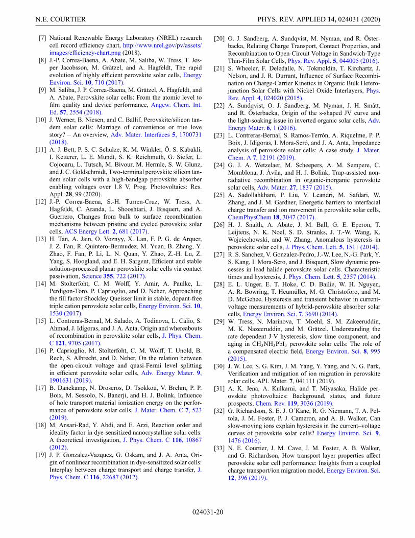
N.E. COURTIER PHYS. REV. APPLIED 14, 024031 (2020)
[7] National Renewable Energy Laboratory (NREL) researchcell record efficiency chart, http://www.nrel.gov/pv/assets/images/efficiency-chart.png (2018).
[8] J.-P. Correa-Baena, A. Abate, M. Saliba, W. Tress, T. Jes-per Jacobsson, M. Grätzel, and A. Hagfeldt, The rapidevolution of highly efficient perovskite solar cells, EnergyEnviron. Sci. 10, 710 (2017).
[9] M. Saliba, J. P. Correa-Baena, M. Grätzel, A. Hagfeldt, andA. Abate, Perovskite solar cells: From the atomic level tofilm quality and device performance, Angew. Chem. Int.Ed. 57, 2554 (2018).
[10] J. Werner, B. Niesen, and C. Ballif, Perovskite/silicon tan-dem solar cells: Marriage of convenience or true lovestory? – An overview, Adv. Mater. Interfaces 5, 1700731(2018).
[11] A. J. Bett, P. S. C. Schulze, K. M. Winkler, Ö. S. Kabakli,I. Ketterer, L. E. Mundt, S. K. Reichmuth, G. Siefer, L.Cojocaru, L. Tutsch, M. Bivour, M. Hermle, S. W. Glunz,and J. C. Goldschmidt, Two-terminal perovskite silicon tan-dem solar cells with a high-bandgap perovskite absorberenabling voltages over 1.8 V, Prog. Photovoltaics: Res.Appl. 28, 99 (2020).
[12] J.-P. Correa-Baena, S.-H. Turren-Cruz, W. Tress, A.Hagfeldt, C. Aranda, L. Shooshtari, J. Bisquert, and A.Guerrero, Changes from bulk to surface recombinationmechanisms between pristine and cycled perovskite solarcells, ACS Energy Lett. 2, 681 (2017).
[13] H. Tan, A. Jain, O. Voznyy, X. Lan, F. P. G. de Arquer,J. Z. Fan, R. Quintero-Bermudez, M. Yuan, B. Zhang, Y.Zhao, F. Fan, P. Li, L. N. Quan, Y. Zhao, Z.-H. Lu, Z.Yang, S. Hoogland, and E. H. Sargent, Efficient and stablesolution-processed planar perovskite solar cells via contactpassivation, Science 355, 722 (2017).
[14] M. Stolterfoht, C. M. Wolff, Y. Amir, A. Paulke, L.Perdigon-Toro, P. Caprioglio, and D. Neher, Approachingthe fill factor Shockley Queisser limit in stable, dopant-freetriple cation perovskite solar cells, Energy Environ. Sci. 10,1530 (2017).
[15] L. Contreras-Bernal, M. Salado, A. Todinova, L. Calio, S.Ahmad, J. Idígoras, and J. A. Anta, Origin and whereaboutsof recombination in perovskite solar cells, J. Phys. Chem.C 121, 9705 (2017).
[16] P. Caprioglio, M. Stolterfoht, C. M. Wolff, T. Unold, B.Rech, S. Albrecht, and D. Neher, On the relation betweenthe open-circuit voltage and quasi-Fermi level splittingin efficient perovskite solar cells, Adv. Energy Mater. 9,1901631 (2019).
[17] B. Dänekamp, N. Droseros, D. Tsokkou, V. Brehm, P. P.Boix, M. Sessolo, N. Banerji, and H. J. Bolink, Influenceof hole transport material ionization energy on the perfor-mance of perovskite solar cells, J. Mater. Chem. C 7, 523(2019).
[18] M. Ansari-Rad, Y. Abdi, and E. Arzi, Reaction order andideality factor in dye-sensitized nanocrystalline solar cells:A theoretical investigation, J. Phys. Chem. C 116, 10867(2012).
[19] J. P. Gonzalez-Vazquez, G. Oskam, and J. A. Anta, Ori-gin of nonlinear recombination in dye-sensitized solar cells:Interplay between charge transport and charge transfer, J.Phys. Chem. C 116, 22687 (2012).
[20] O. J. Sandberg, A. Sundqvist, M. Nyman, and R. Öster-backa, Relating Charge Transport, Contact Properties, andRecombination to Open-Circuit Voltage in Sandwich-TypeThin-Film Solar Cells, Phys. Rev. Appl. 5, 044005 (2016).
[21] S. Wheeler, F. Deledalle, N. Tokmoldin, T. Kirchartz, J.Nelson, and J. R. Durrant, Influence of Surface Recombi-nation on Charge-Carrier Kinetics in Organic Bulk Hetero-junction Solar Cells with Nickel Oxide Interlayers, Phys.Rev. Appl. 4, 024020 (2015).
[22] A. Sundqvist, O. J. Sandberg, M. Nyman, J. H. Smått,and R. Österbacka, Origin of the s-shaped JV curve andthe light-soaking issue in inverted organic solar cells, Adv.Energy Mater. 6, 1 (2016).
[23] L. Contreras-Bernal, S. Ramos-Terrón, A. Riquelme, P. P.Boix, J. Idígoras, I. Mora-Seró, and J. A. Anta, Impedanceanalysis of perovskite solar cells: A case study, J. Mater.Chem. A 7, 12191 (2019).
[24] G. J. A. Wetzelaer, M. Scheepers, A. M. Sempere, C.Momblona, J. Ávila, and H. J. Bolink, Trap-assisted non-radiative recombination in organic-inorganic perovskitesolar cells, Adv. Mater. 27, 1837 (2015).
[25] A. Sadollahkhani, P. Liu, V. Leandri, M. Safdari, W.Zhang, and J. M. Gardner, Energetic barriers to interfacialcharge transfer and ion movement in perovskite solar cells,ChemPhysChem 18, 3047 (2017).
[26] H. J. Snaith, A. Abate, J. M. Ball, G. E. Eperon, T.Leijtens, N. K. Noel, S. D. Stranks, J. T.-W. Wang, K.Wojciechowski, and W. Zhang, Anomalous hysteresis inperovskite solar cells, J. Phys. Chem. Lett. 5, 1511 (2014).
[27] R. S. Sanchez, V. Gonzalez-Pedro, J.-W. Lee, N.-G. Park, Y.S. Kang, I. Mora-Sero, and J. Bisquert, Slow dynamic pro-cesses in lead halide perovskite solar cells. Characteristictimes and hysteresis, J. Phys. Chem. Lett. 5, 2357 (2014).
[28] E. L. Unger, E. T. Hoke, C. D. Bailie, W. H. Nguyen,A. R. Bowring, T. Heumüller, M. G. Christoforo, and M.D. McGehee, Hysteresis and transient behavior in current-voltage measurements of hybrid-perovskite absorber solarcells, Energy Environ. Sci. 7, 3690 (2014).
[29] W. Tress, N. Marinova, T. Moehl, S. M. Zakeeruddin,M. K. Nazeeruddin, and M. Grätzel, Understanding therate-dependent J-V hysteresis, slow time component, andaging in CH3NH3PbI3 perovskite solar cells: The role ofa compensated electric field, Energy Environ. Sci. 8, 995(2015).
[30] J. W. Lee, S. G. Kim, J. M. Yang, Y. Yang, and N. G. Park,Verification and mitigation of ion migration in perovskitesolar cells, APL Mater. 7, 041111 (2019).
[31] A. K. Jena, A. Kulkarni, and T. Miyasaka, Halide per-ovskite photovoltaics: Background, status, and futureprospects, Chem. Rev. 119, 3036 (2019).
[32] G. Richardson, S. E. J. O’Kane, R. G. Niemann, T. A. Pel-tola, J. M. Foster, P. J. Cameron, and A. B. Walker, Canslow-moving ions explain hysteresis in the current–voltagecurves of perovskite solar cells? Energy Environ. Sci. 9,1476 (2016).
[33] N. E. Courtier, J. M. Cave, J. M. Foster, A. B. Walker,and G. Richardson, How transport layer properties affectperovskite solar cell performance: Insights from a coupledcharge transport/ion migration model, Energy Environ. Sci.12, 396 (2019).
024031-20

INTERPRETING IDEALITY FACTORS. . . PHYS. REV. APPLIED 14, 024031 (2020)
[34] M. T. Neukom, A. Schiller, S. Züfle, E. Knapp, J. Ávila,D. P. del Rey, C. Dreessen, K. P. Zanoni, M. Sessolo, H.J. Bolink, and B. Ruhstaller, Consistent device simulationmodel describing perovskite solar cells in steady-state, tran-sient and frequency domain, ACS Appl. Mater. Interfaces11, 23320 (2019).
[35] D. Walter, A. Fell, Y. Wu, T. Duong, C. Barugkin, N. Wu,T. P. White, and K. J. Weber, Transient photovoltage inperovskite solar cells: Interaction of trap-mediated recom-bination and migration of multiple ionic species, J. Phys.Chem. C 122, 11270 (2018).
[36] A. Walsh, D. O. Scanlon, S. Chen, X. G. Gong, and S.-H.Wei, Self-regulation mechanism for charged point defectsin hybrid halide perovskites, Angew. Chem. Int. Ed. 54,1791 (2015).
[37] N. E. Courtier, J. M. Foster, S. E. J. O’Kane, A. B. Walker,and G. Richardson, Systematic derivation of a surfacepolarisation model for planar perovskite solar cells, Eur. J.Appl. Math. 30, 427 (2019).
[38] S. Weber, I. M. Hermes, S. H. Turren Cruz, C. Gort, V. W.Bergmann, L. Gilson, A. Hagfeldt, M. Grätzel, W. Tress,and R. Berger, How the formation of interfacial chargecauses hysteresis in perovskite solar cells, Energy Environ.Sci. 11, 2404 (2018).
[39] I. M. Hermes, Y. Hou, V. W. Bergmann, C. J. Brabec, andS. A. L. Weber, The interplay of contact layers: How theelectron transport layer influences interfacial recombinationand hole extraction in perovskite solar cells, J. Phys. Chem.Lett. 9, 6249 (2018).
[40] M. Cai, N. Ishida, X. Li, X. Yang, T. Noda, Y. Wu, F. Xie,H. Naito, D. Fujita, and L. Han, Control of electrical poten-tial distribution for high-performance perovskite solar cells,Joule 2, 296 (2018).
[41] K. Taretto, New explicit current/voltage equation for p-i-n solar cells including interface potential drops anddrift/diffusion transport, Prog. Photovoltaics: Res. Appl. 22,870 (2014).
[42] The word ectype means a copy or reproduction made in theimage of the archetype or ideal version.
[43] N. E. Courtier, J. M. Cave, A. B. Walker, G. Richardson,and J. M. Foster, IonMonger: A free and fast planar per-ovskite solar cell simulator with coupled ion vacancy andcharge carrier dynamics, J. Comput. Electron. 18, 1435(2019).
[44] C. P. Please, An analysis of semiconductor PN junctions,IMA J. Appl. Math. 28, 301 (1982).
[45] M. J. Ward, L. G. Reyna, and F. M. Odeh, Multiple steady-state solutions in a multijunction semiconductor device,SIAM J. Appl. Math. 51, 90 (1991).
[46] T. Kirchartz, B. E. Pieters, J. Kirkpatrick, U. Rau, andJ. Nelson, Recombination via tail states in polythio-phene:fullerene solar cells, Phys. Rev. B 83, 115209(2011).
[47] S. Ravishankar, O. Almora, C. Echeverría-Arrondo, E.Ghahremanirad, C. Aranda, A. Guerrero, F. Fabregat-Santiago, A. Zaban, G. Garcia-Belmonte, and J. Bisquert,Surface polarization model for the dynamic hysteresis ofperovskite solar cells, J. Phys. Chem. Lett. 8, 915 (2017).
[48] D. A. Jacobs, H. Shen, F. Pfeffer, J. Peng, T. P. White, F. J.Beck, and K. R. Catchpole, The two faces of capacitance:New interpretations for electrical impedance measurementsof perovskite solar cells and their relation to hysteresis, J.Appl. Phys. 124, 225702 (2018).
[49] See Supplemental Material at http://link.aps.org/supplemental/10.1103/PhysRevApplied.14.024031 for tables ofthe parameter values used in this work and an additionalfigure.
[50] S. D. Stranks, G. E. Eperon, G. Grancini, C. Menelaou, M.J. P. Alcocer, T. Leijtens, L. M. Herz, A. Petrozza, andH. J. Snaith, Electron-hole diffusion lengths exceeding 1micrometer in an organometal trihalide perovskite absorber,Science 342, 341 (2013).
[51] Q. Dong, Y. Fang, Y. Shao, P. Mulligan, J. Qiu, L. Cao,and J. Huang, Electron-hole diffusion lengths > 175μm insolution-grown CH3NH3PbI3 single crystals, Science 347,967 (2015).
[52] T. Kirchartz, High open-circuit voltages in lead-halide per-ovskite solar cells: Experiment, theory and open questions,Philos. Trans. R. Soc. A: Math., Phys. Eng. Sci. 377,20180286 (2019).
[53] One might argue that photogenerated electrons only haveto overcome the potential drop V3 to recombine at thePAL-HTL interface, however, the probability of a minoritycarrier recombining depends on the competition betweenextraction and recombination and hence F(V) must takeinto account the positive effect that V1 + V2 has oncharge extraction, transporting photogenerated electronsaway from the PAL-HTL interface and preventing recom-bination. At higher light intensities, when photogeneratedcarriers can no longer be efficiently extracted from the PAL,the potential barrier for this type of recombination mayreduce to V3.
[54] MATLAB, MATLAB version 9.3.0.713579 (R2017b)(2017).
[55] N. E. Courtier, G. Richardson, and J. M. Foster, A fast androbust numerical scheme for solving models of charge car-rier transport and ion vacancy motion in perovskite solarcells, Appl. Math. Model. 63, 329 (2018).
024031-21