introducing the research centers for solar energy … introducing the research centers for solar...
TRANSCRIPT

1
Introducing the Research Centers for Solar Energy Harvesting
1. Research Center for Next-generation Thin Film Solarcells, funded by MKE, Korea
2. Pioneer Research Center (PRC) for Solar Thermal Conversion Nanodevices, funded by MEST, Korea
Jung-Ho Lee, Professor and Director
Hanyang University

2
Research Center for Next-generation Thin Film Solarcells
• Towards the next-generation thin film solarcell using silicon wires
Jung-Ho Lee (PI), Bongyoung Yoo, Jong-Ryoul Kim, Yong-Ho Choa, Yongwoo ChoHanyang University
Collaborated withYonsei University, KIMM, NNFC, Korea Institute for Energy Research, Sungkyunk
wan University, Ewha Women’s University
차세대박막태양전지원천기술연구센터

3
Motivation
Tapered SiNWs SiMWs
Antireflection (AR) roleè Enhancement
of optical absorption
Radial p-n junction of MWs èutilization of low-purity silicon
enabling short diffusion of carriers
Very dense tapered NWs co-integrated with periodic MW arrays
High efficiency solar cell
Combining the AR enhancement of dense NWs and the radial p-n junctions of sparse MWs.

4
3. 대상기술의 원천성 및 객관성
+-
~1/α
~Ln
~Ln = 50~100 ㎛
Planar p-n junction solarcell Radial p-n junction solarcell
Radial p-n junction wired solarcell<Vertically aligned nanowires>
1. Strong broadband optical absorption
à Light trapping enhancement in between nanowires (NWs)
2. More light absorption due to Graded-refractive-index (GRI) effect using tapered NWs
< Radial p-n junction microwires>
3. Long absorption paths & short distances for carrier collection
à Orthogonal separation of carriers to a sunlight direction
4. Large surface areas for light harvest
Atwater group, J. Appl. Phys. 97, 114302 (2005)

5
Very dense, vertical SiNWs prepared by Ag induced etching
HF(4.6M) + H2O2 (0.44M) 20min (0.5 um/min)
AgNO3 (0.01M) + HF(4.6M)
P-Si(100) 1-10 ΩCm
Ag removal – nitric acid
• Simple, Cost-effective, Room temperature approach• Waferscale fabrication of vertical SiNWs with a 20-200 nm diameter range • Highly uniform feature across the wafer• Easy agglomeration at the tops of NWs upon drying
Deposition of Ag particles Ag induced vertical etching
Ag deposition Ag induced etching Ag removal
Agglomeration
6
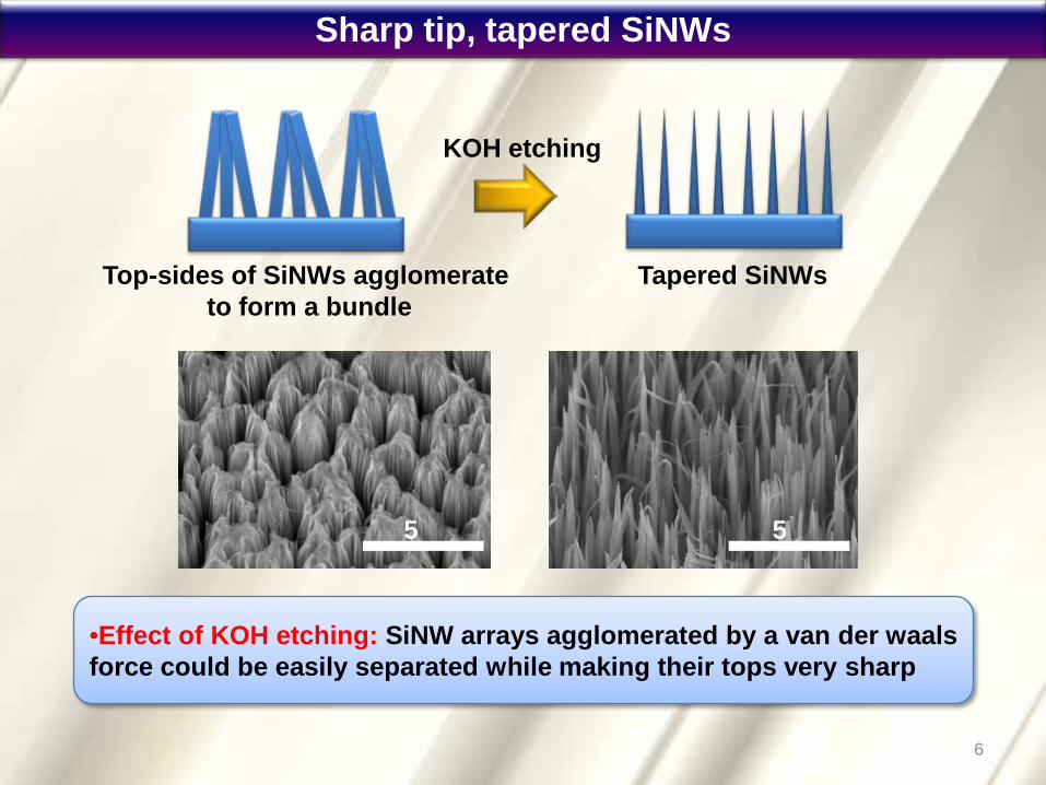
Sharp tip, tapered SiNWs
KOH etching
Tapered SiNWsTop-sides of SiNWs agglomerate to form a bundle
5㎛ 5㎛
•Effect of KOH etching: SiNW arrays agglomerated by a van der waalsforce could be easily separated while making their tops very sharp
7
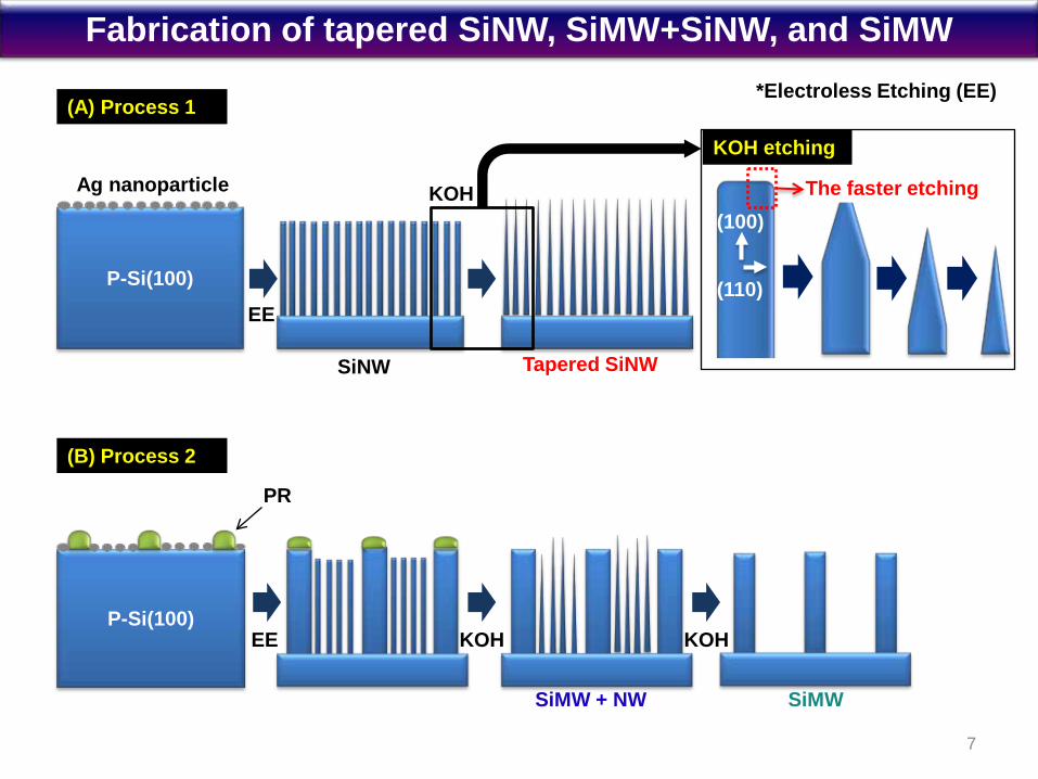
P-Si(100)
P-Si(100)
SiNW Tapered SiNW
SiMW + NW SiMW
PR
Ag nanoparticle
(B) Process 2
(A) Process 1
(100)
(110)
The faster etching KOH
KOH KOH
*Electroless Etching (EE)
EE
EE
KOH etching
Fabrication of tapered SiNW, SiMW+SiNW, and SiMW

8
Increasing the KOH etching time
Morphological variation of tapered SiNWs with KOH etching time
0s 10s 15s 30s
• Initially, the corner sides of NWs strongly attacked by KOH becausethe complicated high-index surfaces develop easily.• Finally, sharp-tip, tapered SiNW arrays with (111) side planes remainsbecause the etching rate of those planes is slowest.
1 ㎛ 1 ㎛ 1 ㎛ 1 ㎛
Faster etching region
(100)
(110)
(111)
KOH etching rate at RT:24nm/min for (100),35nm/min for (110)

9
KOH 0s KOH 120s
KOH 180sKOH 240s
Co-integrated wire structure of SiNW+SiMW
10㎛
KOH etching could reduce the areal density of NWs whileimproving the surface roughness of NW.Diameter of MWs normally decreases from ~2 ㎛ to 1.75 ㎛while KOH etching for 240 s.
MW + NW MW + tapered NW
MW MW + tapered NW
KOH
KOH
KOH
KOH
KOH

10
Waferscale fabrication of SiNWs+MWs
Waferscale uniformity of the co-integrated wire structure
Waferscale co-integrated SiNW+MW arraysshow the black color due to excellentabsorption.
top bottom4in wafer
centerBlack surface

11
Fabrication of p-n junction
Doping method: Spin-on-doping (SOD)
<Doping mechanism of pSOD>
2P2O5 + 5Si à 5SiO2 + 4P
Solid-state diffusion: Predeposition followed by drive-in
P2O5 SiO2
P
Si dummy wafer
Phosphorous-SOD

12
Fabrication of p-n junction using SOD
Bulk or radial p-n junction forms depending upon wire diameters
Tapered SiNWs
SiMWs
MWs+NWs
Bulk p-n junction
Radial p-n junction
Radial and bulk p-n junction0 500 1000 1500 2000
Conc
entra
tion
(ato
ms/
cc)
Sputter Depth (nm)
1015
1016
1017
1018
1019
1020
1021
1022
Dummy wafer
Dummy waferBoron-SOD
Phosphorous-SOD
Phosphorous (top)
Boron (bottom)

130 250 500 750 10001014
1015
1016
1017
1018
1019
1020
1021
1022 B P
Conc
entra
tion(
atom
s/cc
)
Sputter Depth(nm)
n p np
n
Junction Depth of ~500nm
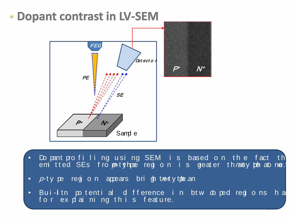
v LVSEM images clarify the formation of a radial
p(core)-n(shell) junction inside the Si wire.
v The vanishing contrast at high accelerating voltage
is due to the dominance of the energetic
backscattered electrons (BSE) and their
respectively generated SEs.
Low-voltage SEM images of a radial p-n junction MW
14
• Dopant profiling using SEM is based on the fact that the amount of emitted SEs from the p-type region is greater than that of n-type one.
• p-type region appears brighter than n-type.
• Built-in potential difference in btw doped regions has been suggested for explaining this feature.
PE
SE
Detector
P+ N+
FEG
Sample

15
0.5 kV, 10 mm, 15 μA 1 kV, 10 mm, 15 μA 5 kV, 10 mm, 15 μA
n+
p+
n+
p+
P-sub.
n+
p+
n+
p+
P-sub.
n+
p+
n+
p+
P-sub.
Signa
l In
tens
ity
Depth (μm)
l Accelerating Voltage ↑, dopant contrast ↓
l Contrast can be obtained between 0.5-5 kV
0.5 1.0 1.5 2.0 2.5 3.0
0.5 kV1 kV5 kV
n+ p+ n+ p+ P-sub.

16
1 kV, 15 mm, 2 μA
n+
p+
n+
p+
P-sub.
1 kV, 15 mm, 7 μA
n+
p+
n+
p+
P-sub.
Signa
l In
tens
ity
Depth (μm)0.5 1.0 1.5 2.0 2.5 3.0
2 μA7 μA
15 μA
n+ p+ n+ p+ P-sub.
l Electron beam current ↑, dopant contrast ↑
l Contrast can be obtained between 0.5-20 μA
1 kV, 15 mm
n+
p+
n+
p+
P-sub.
15 μA 20 μA
17
400 800 1200 1600 2000 24000
10
20
30
40
Ref
lect
ance
(%)
Wavelength (nm)
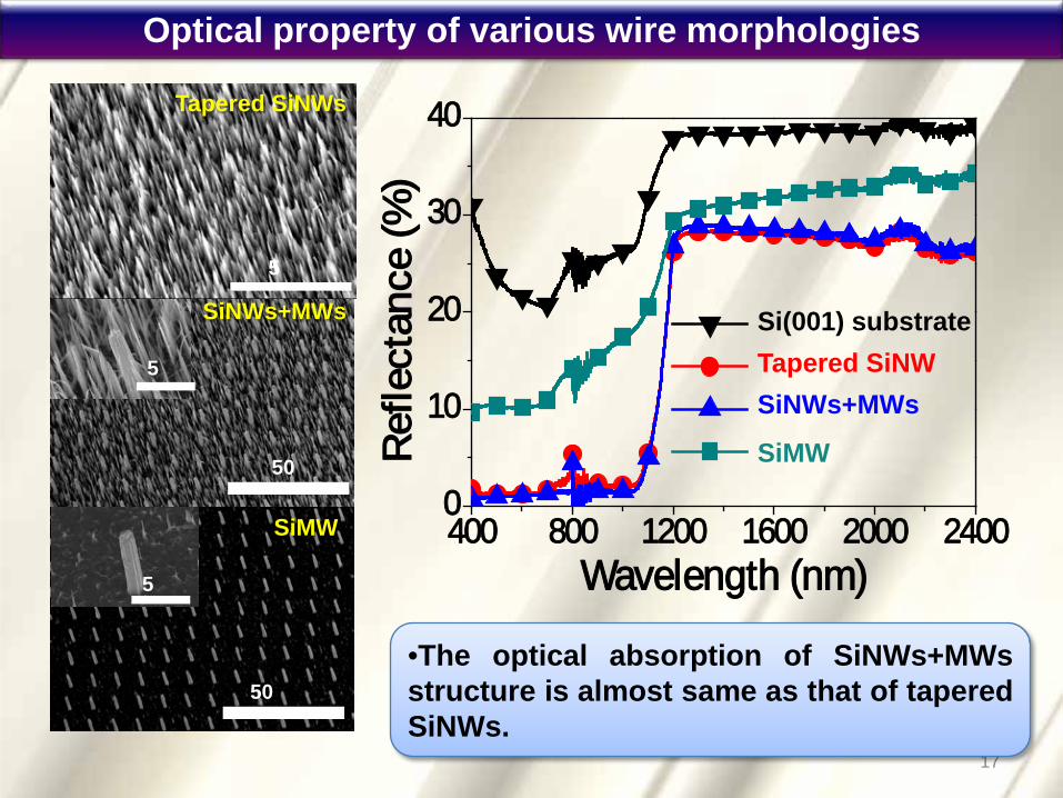
Optical property of various wire morphologies
•The optical absorption of SiNWs+MWsstructure is almost same as that of taperedSiNWs.
50㎛
50㎛50㎛
5㎛
Tapered SiNWs
5 ㎛
SiNWs+MWs
SiMW
5㎛
SiNWs+MWsTapered SiNWSi(001) substrate
SiMW

18
DC bias Pulsed 1kV
Dopant PH3 30 sccm
RF power 1kHz
Time 60s
Annealing 900°C 30sec
Dose 3e15
•Intensifying theN+-level of theMW shells whileenabling shallow,conformal doping
p-type wafer
Plasma ion doping
Additional Doping: Plasma Ion Doping (PID)
19
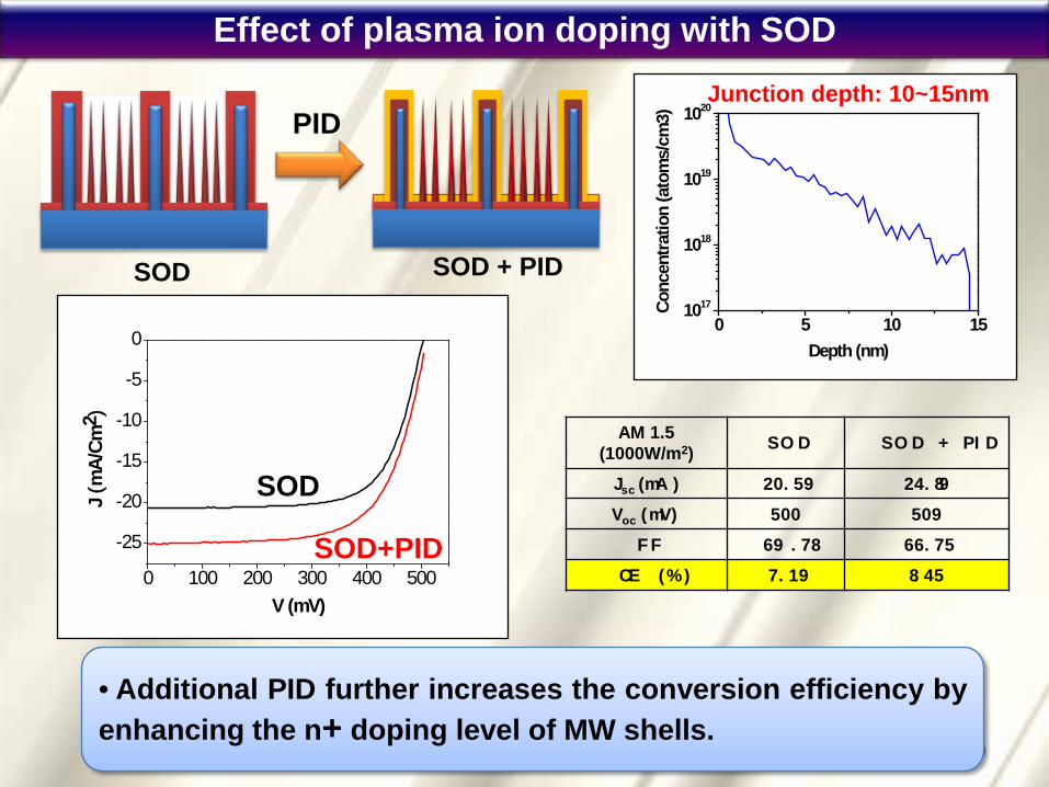
Effect of plasma ion doping with SOD
AM 1.5(1000W/m2) SOD SOD + PID
Jsc (mA) 20.59 24.89
Voc (mV) 500 509
FF 69.78 66.75
CE (%) 7.19 8.45
• Additional PID further increases the conversion efficiency byenhancing the n+ doping level of MW shells.
SOD SOD + PID
PID
0 100 200 300 400 500
-25
-20
-15
-10
-5
0
J (m
A/Cm
2 )
V (mV)
0 5 10 151017
1018
1019
1020
Conc
entra
tion
(ato
ms/
cm3)
Depth (nm)
Junction depth: 10~15nm
SOD
SOD+PID

2020
PV cell efficiencyConve
rsio
n E
ffic
iency
(%
)
8
6
7
9
Jsc 27.01
Voc 497
FF 66.97
0 100 200 300 400 500-30
-25
-20
-15
-10
-5
0
J (m
A/Cm
2 )
V (mV)
• Tapered Si NW
• Planar junction
• Tapered Si NW
• Radial junction Si MW• Tapered Si NW
• p-n-n+ radial junction Si MW
6.56 %
7.19 %
9.10 %
2010. 2
2008. 07
2008. 12
5. Summary

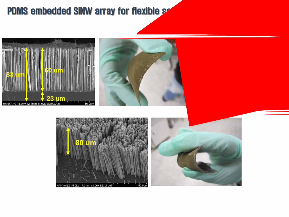
83 um 60 um
23 um
80 um
현재 12 X 12 cm2에서 박막화 공정 가능

500 1000
0
20
40 PDMS Si wire embedded PDMS
Asor
ptio
n (%
)
Wavelength (nm)
Detachment of PDMS embedded wire array Flexible solar cell application
50㎛
30㎛

v Square mold를 활용할 경우, PDMS curing후 대면적 (³10X10 cm2)에서
저비용으로 우수한 박막 탈착이 가능.
v UMG(4N~6N) thin wafer (20~50 mm)를 활용한 우수한 원가 경쟁력
용이한 대면적 박막 구현 및 뛰어난 원가 경쟁력 확보
< 대면적 박막 구현> < UMG thin wafer활용>
24
Si 나노구조 기반 태양발전 소자의 제조 및 평가
GlassITO
GlassITO
MetalWafer removal

0 500 1000 1500 2000 25000
20406080
100
020406080100
Tra
nsm
ittan
ce (%
)
Refle
ctan
ce (%
)
Waveletngh (nm)
R,10g T10g R,15g T,10g
0 500 1000 1500 2000 25000
20406080
100
Abso
rptio
n (%
)
Wavelength (nm)
A,10g A,15g
•
v The reflectance, transmittance, and absorption spectra of PDMS film show its possibility
to solar cell application.
v An excellent light absorption of 90% is occurred in the NIR region.
v Accordingly, the incident light wave can easily penetrate through the PDMS film , reaching
the Si wire arrays and interacting with it.

400 800 1200 1600 20000
20
40
Re
flect
ion
(%)
Wavelength (nm)400 800 1200 1600 2000
0
20
40
60
80
Tran
smis
sion
(%)
Wavelength (nm)
400 800 1200 1600 20000
20
40
60
80
100
Abso
rptio
n (%
)
Wavelength (nm)
Reflection Transmission
Absorption
PDMS
SiNW
PDMS
SiNW
Al(300nm)
PDMS/SiNWs ((L~4 mm) w/Si sub
PDMS/SiNWs (L~4 mm) w/o subPDMS/SiNWs (L~12 mm) w/o sub
PDMS/SiNWs (L~16 mm) w/o sub

NNLT 5, 1081 (2005)
Ge NP on Si MW (한양대)
Appl. Phys. Lett., 83, 1258 (2003)
Ge effect
i-Si
elec
tron el
ectr
on
n-Si Low impurity
Formation of P+ emitter p+-Si; I layer by PECVD
CdSeor
CGTSor Ge

28
Pioneer Research Center (PRC) for Solar Thermal Conversion Nanodevices
• Towards the nanoconvergence btw wired solarcell (top) and
nanostructured thermoelectric (bottom)
Jung-Ho Lee (PI), Bongyoung Yoo, Jong-Ryoul KimHanyang University
Collaborated withKyu-Hwan Lee (KIMS), Youngkyoo Kim (Kyoungpook National University), Jaehyun Kim (DGIST), Hyoung-Koun Cho (Sungkyunkwan University), Dongwook Kim (Ewha Women’s University), Minwook Oh (KERI), Nosang V. Myung (UCRiverside),
Choongho Yu (Texas A&M University)
태양광열전나노소자파이오니어융합연구단
Pioneer Research Center for Solar Thermal Conversion Nanodevices
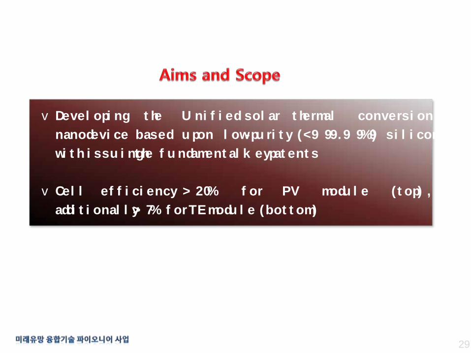
vDeveloping the Unified solar thermal conversionnanodevice based upon low-purity (<99.9999%) siliconwith issuing the fundamental key patents
vCell efficiency >20% for PV module (top),additionally >7% for TE module (bottom)
29

Si/SiGe Microwire
Nanostructured BiSbTe
• 금속나노선이 일방향 삽입된
BiTe 나노구조체를 이용하여 낮은
(≤100°C) 온도구배에서 높은
TE 전환율 (ZT³1.5) 확보 가능
Device convergence with nanomaterials
• MW 어레이에 의한 multi-scattering효과로 태양광 반사 방지막 기능 부여
• MW 내에 radial p-n junction을만드는 신개념으로 저순도(99.99%) 실리콘을 활용하여, 기존 기술대비 기판단위면적당 실제 p-n junction 면적의대폭 증가 가능
당 연구단 결과Electrochem. Comm. 2008
ECS Fall, 2008
30
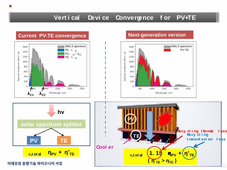
31
ηc,total ≒ 1.15 x ηPV + η’TE( η’TE > ηTE )
Vertical Device Convergence for PV+TE
solar spectrum splitter
PV TE
hν
ηc,total ≒ ηPV + η’TE
TE
PV 열투과
Recycling thermal lossRecycling transmission loss
수직형 PV-TEAM1.5 spectrum AM1.5 spectrum
TE : < λC1
PV : λC1~ λC2TE : > λC2
λC1 λC2
Cooler 역할
Current PV-TE convergence Next-generation version

v 효율 추정 조건 : Hot zone 온도 = 100 °C , Cold zone 온도 = 23 °C
(ΔT = 77 °C), ZT = 2
v 단위면적당 총 이동 열전달 양은 782.6 W/m2
v TH=100 °C인 경우에 ZT=2를 갖는 소재를 채용시 ZT에 따른 발전용량은 46 W/m2
이며, 이는 열전효율 ~7%에 대응하는 결과로 도출됨
나노복합 열전소자의 PV-TE 통합소자 내 발전 효율 평가
총 열전달양682.6 W/m2
열전효율~ 7 %
32

33
세부추진분야 연구원구성 최근 출간저널
WG1
Device
Convergence
WG2
PV device
and
Measurement
WG3
TE device
and
Measurement
PV & TE device의
융합을 위한 산학연
반도체 소자 및
공정 전문가
Si wired solar cell
제작 을 위한 태양전지,
유무기합성 및
Si 나노구조 전문가
BiTe nanostructured
TE소자 제작을 위한 BiTe
열전소자, 측정, 유기,
전기화학 산학연 전문가
• 이정호: 한양대
• 김동욱: 이화여대
• 손영수: 대구가톨릭대
• 조용우: 한양대
• 조형균: 성균관대
• 김영규: 경북대
• 김재현: 대구경북과학기술원
• 김종렬: 한양대
• 이규환: 재료연구소
• 오민욱: 한국전기연구원
• C. Yu: Texas A&M Univ.
• 유봉영: 한양대
• N. V. Myung: UC Riverside
•임동찬: 재료연구소(註) * 신진연구자전체15명 중 10명
34
Acknowledgements
• Pioneer Research Center for Solar Thermal Conversion Nanodevices, funded by MEST, Korea
• Research Center for Next-generation Thin Film Solarcells, funded by MKE, Korea
• Also supported by National Nanofab Center
Thank you for your attention!