introduction of new igbt generation 7 - semikron
TRANSCRIPT
© by SEMIKRON / 2019-10-10 / Application Note PROMGT.1023/ Rev.7/ Template Application Note
Page 1/15
Introduction of new IGBT Generation 71. Introduction .............................................................................................................................1
1.1 General Introduction.............................................................................................................11.2 Chip Technology ..................................................................................................................21.3 Main Advantages of IGBT Generation 7 based Power Modules.....................................................21.4 Parameter Overview .............................................................................................................2
2. Application of Generation 7 IGBT.................................................................................................32.1 Switching behaviour .............................................................................................................3
2.1.1 Turn-on ........................................................................................................................32.1.2 Turn-off ........................................................................................................................42.1.3 Switching loss dependency on temperature, voltage and current ..........................................62.1.4 Short circuit ..................................................................................................................6
2.2 Gate Capacitance .................................................................................................................72.3 Operation junction temperature up to 175°C............................................................................8
2.3.1 Further considerations for operation at higher junction temperatures ....................................92.4 HV-H3TRB Robustness ..........................................................................................................92.5 Practical recommendations ..................................................................................................10
2.5.1 Chip shrinkage and current rating...................................................................................102.5.2 Cross-reference to IGBT4 based power modules ...............................................................102.5.3 Gate resistor selection ..................................................................................................102.5.4 Repetitive peak collector current ....................................................................................10
3. Performance comparison ..........................................................................................................113.1 MiniSKiiP ...........................................................................................................................113.2 SEMiX3p ...........................................................................................................................11
4. Summary ...............................................................................................................................12
1. Introduction
1.1 General IntroductionWith this document SEMIKRON like to introduce the 1200V Generation 7 IGBT chips and their rollout to different power module packages. The new chip generation will be implemented from two independent sources. One source is Infineon which can be identified by the index “T7”. The second source is a new chip supplier for SEMIKRON, which can be identified by the index “M7”. Both IGBT types will be combined with the well-established SEMIKRON CAL4F freewheeling diode. With the multiple chip source strategy, it is possible to select the best chip performance for the individual packaging platforms. Since the T7 IGBT has been optimized for low to medium power motor drive applications it will be first introduced in the low to medium power packages MiniSKiiP® and SEMITOP®. The
Application Note
AN 19-002
Revision: 01 Issue date: 2019-10-10Prepared by: Arendt Wintrich, Peter BeckedahlApproved by: Ulrich Nicolai
Keyword: IGBT, Gen7, Switching Behaviour, Cross Reference

© by SEMIKRON / 2019-10-10 / Application Note PROMGT.1023/ Rev.7/ Template Application Note
Page 2/15
M7 IGBT is well suited for paralleling hence it will be introduced to the larger power module families SEMiX® and SEMITRANS®.
1.2 Chip TechnologyThe new chip generation is based on a significant increased cell density in conjunction with striped trench gate structures. The paralleled trench cell layout consists of active and passive trenches, which enable smaller cell pitches and very narrow mesa structures. This cell concept allows for higher carrier storage close to the emitter electrode, which leads to a significant increase in electrical conductivity in the drift zone. The main benefit is a substantial reduction of the forward voltage drop of up to 400mV compared to former chip generations based on squared trench cells, while the switching losses remain at a similar level like before.
Figure 1: Previous squared trench cell design and new striped trench gate structure
1.3 Main Advantages of IGBT Generation 7 based Power ModulesDue to reduced power losses, the new chip generation allows for a significant power density increase of up to 33%. A further power density increase can be obtained for overload conditions by raising the maximum chip operation temperature to 175°C. Next to the power density another important benefit is the improved environmental robustness of the new chip generation. The new chips pass the harsh HV-H3TRB (High Voltage, High Temperature, High Humidity Reverse Bias) test that assures reliable operation in hot and humid environment. Main advantages are:
20% lower on-state voltage Operation junction temperature of 175° during overload High humidity robustness 33% higher power density in same package 8µs short circuit robustness Safe operation with 0 volts gate turn-off
1.4 Parameter OverviewFigure 2 gives an overview of the relevant chip parameters for different chip types. The on-state voltage reduction allows for a 25% chip shrinkage at same current rating. As a trade-off for the superior power density, the short circuit withstand time tSC had to be reduced to 8µs. This is already known from other recent chip generations and still provides sufficient safety margins for modern protection topologies.
© by SEMIKRON / 2019-10-10 / Application Note PROMGT.1023/ Rev.7/ Template Application Note
Page 3/15
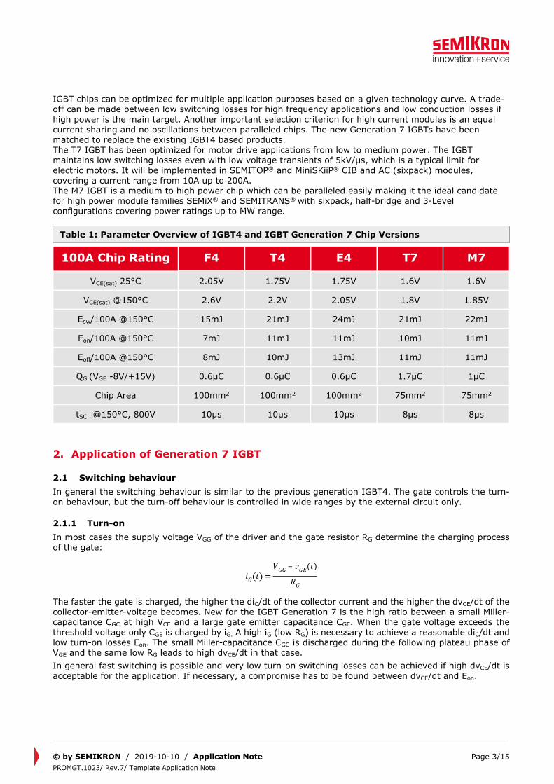
IGBT chips can be optimized for multiple application purposes based on a given technology curve. A trade-off can be made between low switching losses for high frequency applications and low conduction losses if high power is the main target. Another important selection criterion for high current modules is an equal current sharing and no oscillations between paralleled chips. The new Generation 7 IGBTs have been matched to replace the existing IGBT4 based products. The T7 IGBT has been optimized for motor drive applications from low to medium power. The IGBT maintains low switching losses even with low voltage transients of 5kV/µs, which is a typical limit for electric motors. It will be implemented in SEMITOP® and MiniSKiiP® CIB and AC (sixpack) modules, covering a current range from 10A up to 200A. The M7 IGBT is a medium to high power chip which can be paralleled easily making it the ideal candidate for high power module families SEMiX® and SEMITRANS® with sixpack, half-bridge and 3-Level configurations covering power ratings up to MW range.
Table 1: Parameter Overview of IGBT4 and IGBT Generation 7 Chip Versions
100A Chip Rating F4 T4 E4 T7 M7
VCE(sat) 25°C 2.05V 1.75V 1.75V 1.6V 1.6V
VCE(sat) @150°C 2.6V 2.2V 2.05V 1.8V 1.85V
Esw/100A @150°C 15mJ 21mJ 24mJ 21mJ 22mJ
Eon/100A @150°C 7mJ 11mJ 11mJ 10mJ 11mJ
Eoff/100A @150°C 8mJ 10mJ 13mJ 11mJ 11mJ
QG (VGE -8V/+15V) 0.6µC 0.6µC 0.6µC 1.7µC 1µC
Chip Area 100mm2 100mm2 100mm2 75mm2 75mm2
tSC @150°C, 800V 10µs 10µs 10µs 8µs 8µs
2. Application of Generation 7 IGBT
2.1 Switching behaviourIn general the switching behaviour is similar to the previous generation IGBT4. The gate controls the turn-on behaviour, but the turn-off behaviour is controlled in wide ranges by the external circuit only.
2.1.1 Turn-onIn most cases the supply voltage VGG of the driver and the gate resistor RG determine the charging process of the gate:
𝑖𝐺(𝑡) =𝑉𝐺𝐺 ‒ 𝑣𝐺𝐸(𝑡)
𝑅𝐺
The faster the gate is charged, the higher the diC/dt of the collector current and the higher the dvCE/dt of the collector-emitter-voltage becomes. New for the IGBT Generation 7 is the high ratio between a small Miller-capacitance CGC at high VCE and a large gate emitter capacitance CGE. When the gate voltage exceeds the threshold voltage only CGE is charged by iG. A high iG (low RG) is necessary to achieve a reasonable diC/dt and low turn-on losses Eon. The small Miller-capacitance CGC is discharged during the following plateau phase of VGE and the same low RG leads to high dvCE/dt in that case. In general fast switching is possible and very low turn-on switching losses can be achieved if high dvCE/dt is acceptable for the application. If necessary, a compromise has to be found between dvCE/dt and Eon.

© by SEMIKRON / 2019-10-10 / Application Note PROMGT.1023/ Rev.7/ Template Application Note
Page 4/15
Figure 2: Turn-on at IC(nom)=100A, VCC=600V, Tj=150°C and RG=1.6
When comparing statements about dvCE/dt it is important to know the definition for the measurement conditions. A measurement between 90% and 10% of VCC results in lower values, possibly only 2/3 of a 80%...20% measurement. Measurements in a window around 30% of VCC would result in the highest dvCE/dt values. Figure 3 shows typical dvCE/dt values for the commonly used 10%-90% VCC definition of a 100A IGBT T7. At low temperatures and low currents the dvCE/dt has the highest value. IGBT M7 shows a similar behaviour, but for different external gate resistor values because the internal RG(int) and the gate charge QG are different.
Figure 3: dvCE/dt behaviour at turn-on for different conditions
2.1.2 Turn-offUnder nominal switching conditions the gate channel is already closed (vGE(t) < VGE(th)) before VCE starts to rise and before IC starts to fall (see Figure 4). The high amount of charge carriers in the base of the semiconductor is comparable to a big capacitor Cn-base, which feeds the collector current. The turn-off behaviour is independent from RG in a certain range typically given in data sheet characteristics. Only a different turn-off delay time in the gate voltage (violet) is visible when changing RG. Nevertheless the time response of IC (blue) and VCE (green) are identical for RG=1.6 and RG=10. Consequently also the turn-off losses are almost independent of RG. The two curves are shifted slightly to see that both voltage and current signals are running in parallel. At turn-off the IC determines the dvCE/dt: the higher the IC is, the faster Cn-
base is discharged; low currents lead to low dvCE/dt.
CGE is charged limits diC/dt CGC is discharged limits dvCE/dtVCE
VGE
IC

© by SEMIKRON / 2019-10-10 / Application Note PROMGT.1023/ Rev.7/ Template Application Note
Page 5/15
Figure 4: Turn-off at IC(nom)=100A, VCC=600V, Tj=150°C and RG=1.6 compared to 10
At turn-off the dvCE/dt is highest at low temperatures and maximum current. In the example in Figure 5, the dvCE/dt increases by 50% from 3.4kV/µs at Tj=150°C to 5.1kV/µs at 25°C.
Figure 5: Turn-off at IC(nom)=100A, VCC=600V, RG=1.6 Tj=25°C and Tj=150°C
150°C
25°CVCE
VGE
IC
The delay time increases for even higher RG and free charge carriers disappear during that time. This leads to less tail current and an increased diC/dt with a higher turn-off overvoltage (red range in Figure 6). A gate controlled turn-off behaviour is achievable only for very high RG values but to the disadvantage of high switching losses and a very long delay time in active mode. Therefore relative low RG values are recommended to assure low switching losses and a low overvoltage.
10
1.5
VCE
VGE
IC

© by SEMIKRON / 2019-10-10 / Application Note PROMGT.1023/ Rev.7/ Template Application Note
Page 6/15
Figure 6: Principle behaviour of turn-off overvoltage for different RG at Tj=25°C and Tj=150°C
150°C
25°C
Turn-off overvoltage = f(RG)
RG
VCE(
peak
)
2.1.3 Switching loss dependency on temperature, voltage and currentInterdependencies of various parameters are necessary for loss calculation and simulation (see [2], page 277ff). While the dependencies on current and gate resistor are stated in the data sheet, dependencies on voltage and temperature are missing. The voltage dependency is almost linear for both IGBTs (voltage exponent around 1) and thereby much lower compared to former generations. The switching losses at room temperature are roughly 40% lower compared to 150°C (TC~0.003·1/K)
Figure 7: Dependencies of switching losses from operation conditions Esw=Eon+Eoff
2.1.4 Short circuitBoth Generation 7 IGBTs are able to turn-off a short circuit current. Due to the chip shrinkage and therewith a lower thermal chip capacity the short circuit pulse duration tSC is shorter than with former IGBT generations. It is specified for VCC=800V and VGE=15V with tSC=8µs at 150°C and tSC=7µs at 175°C.This statement specifies a certain energy ESC = ISC·VCC ·tSC. The short circuit current is self-limiting at VGE=15V and Tj=150°C to about 4·IC(nom) (i.e. ESC=2.56J for a 100A chip). Short circuit parameters can be varied to some extend while keeping the energy constant, like shown in the two following examples. The influencing factors can be superimposed. In example 1 the DC-link voltage is only 600V instead of 800V and by this the tsc can be increased to:
. 𝑡𝑆𝐶(600𝑉) = 𝑡𝑆𝐶(800𝑉) ∙800𝑉600𝑉 = 10.6µ𝑠
Ran
ge o
f no
min
al R
G
Ran
ge o
f in
crea
sed
di/d
t
Ran
ge o
f ga
te c
ontr
olle
d sw
itchi
ng

© by SEMIKRON / 2019-10-10 / Application Note PROMGT.1023/ Rev.7/ Template Application Note
Page 7/15
In example 2 a higher short circuit current is considered, because the IGBT might be controlled by a higher gate voltage. The current is increased by 25% (5·IC(nom)) at VGG=17V and tsc has to be reduced consequently to:
. 𝑡𝑆𝐶(17𝑉) = 𝑡𝑆𝐶(15𝑉) ∙4 ∙ 𝐼𝐶(𝑛𝑜𝑚)
5 ∙ 𝐼𝐶(𝑛𝑜𝑚)= 6.4µ𝑠
Figure 8: Short circuit of IC(nom)=100A chips at VCC=800V, Tj=150°C
Short circuit turn-off with nominal RG without any clamping or soft turn-off option is possible in many cases. A low inductance, state of the art DC-link is mandatory but it is necessary to verify the short circuit performance in the final application setup.
2.2 Gate CapacitanceThe Generation 7 IGBT chips have a significant higher gate capacitance compared to previous IGBT generations due to the new striped trench gate structure. Depending on the gate turn-on and turn-off voltages this might lead to higher gate charges, compared to former chip generations (see Table 1). The gate input capacitance Cies is divided into the gate-emitter capacitance CGE and the gate-collector (Miller) capacitance CGC. Figure 9 shows the equivalent circuit diagram of an IGBT including the parasitic capacitors. The increased Cies value can be solely attributed to an increased CGE value while the Miller capacitance CGC remains at a low level. The combination of a large gate-emitter and a relatively small gate-collector capacitance makes the IGBT Generation 7 very robust against undesired parasitic turn-on. This effect is usually induced from diode switching transients, which charge the gate through the Miller capacitance [3].Additional external gate-emitter capacitors or a negative turn-off gate voltage to keep the gate at a safe state are not necessary for many applications. Small to medium size power modules can be well controlled with a unipolar gate supply voltage of +15V / 0V [4]. A unipolar supply voltage keeps the driver design simple and reduces the required driver power to similar levels needed for former chip generations [3].The required gate drive power is calculated with the equation below. QG depends on the chosen gate drive voltages and can be derived from the graphs in the datasheet.
𝑃𝐺𝐷(𝑜𝑢𝑡) = 𝑄𝐺 ∙ (𝑉𝐺(𝑜𝑛) ‒ 𝑉𝐺(𝑜𝑓𝑓)) ∙ 𝑓𝑠𝑤
VCE
tSC=8µs
VGE
IC

© by SEMIKRON / 2019-10-10 / Application Note PROMGT.1023/ Rev.7/ Template Application Note
Page 8/15
Figure 9: Equivalent circuit diagram of IGBT and capacitive elements
2.3 Operation junction temperature up to 175°CThe new Generation 7 IGBTs allow a maximum operation at Tj(op)-ol=175°C during overload. Figure 10 shows details of the maximum temperature definition and the allowed load profile. The nominal continuous operation is limited to a maximum junction temperature of Tj(op)=150°C. However to match typical motor drive overload profiles it is allowed to exceed Tj(op)=150°C to up to Tj(op)-ol=175°C for an absolute maximum time of t1=60s. In addition the overload duration is limited to a maximum duty cycle of 20%. Example: The overload time t1 is limited to an absolute maximum duration of 60s, so the minimum permissible cycle time T is 300s or larger. If the load cycle time T is 25s the permissible overload with 150°C<Tj(op)-ol<=175°C is limited to t1<=5s.
Figure 10: Definition of maximum operational junction temperature
It is important to notice that the maximum junction temperature should never exceed 175°C including the temperature ripple originating from the fundamental output frequency. The lower the fundamental output frequency of an inverter the higher the temperature ripple in the junction becomes. The effect can be seen in Figure 11 for a standard 2-level inverter on an air-cooled heatsink. At nominal load the fundamental output frequency is set to 50Hz which results in a moderate junction temperature swing of 7K. During overload condition, the current is increased and at the same time also the fundamental output frequency is reduced to 10Hz. This leads to a temperature swing of more than 25K. The example on the left fulfils the defined overload conditions: The junction temperature never exceeds 175°C, exceeds 150°C for less than 60s and the duty cycle is lower than 20%.The example on the right does NOT fulfil the defined overload conditions: The junction temperature is even lower than in the previous example, but the junction temperature exceeds 150°C for about 90s. Additionally the duty cycle is 30%.

© by SEMIKRON / 2019-10-10 / Application Note PROMGT.1023/ Rev.7/ Template Application Note
Page 9/15
Figure 11: Example of acceptable and not acceptable overload condition
Acceptable Overload Condition Not Acceptable Overload Condition
This overload definition is in particular beneficial for drives with well-defined load cycle conditions. Also fault situations e.g. low voltage ride-through can be covered without limiting the nominal operation.
2.3.1 Further considerations for operation at higher junction temperaturesHigher junction temperatures will lead to higher heatsink temperatures, which could imply additional limitations for the power module as well as other system components:
- Solder and wire bond connections in power modules are aging over time. The dominating factor is the junction temperature swing during load cycles. This is particular critical for servo and elevator drives as well as wind turbines. It is recommended to perform a lifetime calculation based on the mission profile of critical applications in order to verify the expected service life.
- An additional limitation is the maximum permissible power module case (or plastic housing) temperature, which can be found in the module datasheet. This can be in particular critical for long overload durations of air-cooled systems where the heatsink is subject to an additional temperature rise.
- The maximum heatsink temperature underneath the power module will also effect the Thermal Interface Material (TIM). Please check the maximum permitted operation condition in the relevant TIM datasheet. [5]
- Power modules with higher power density and higher maximum junction temperature allow for a higher inverter current in the same footprint. This could lead to additional losses and heating in bus bars or the power PCB. Losses in the PCB and maximum temperatures of the PCB components need careful considerations. High temperature PCB materials, wider copper tracks, thicker copper layers or additional number of layers as well as thermal vias should be taken into account.
2.4 HV-H3TRB RobustnessAnother major benefit of the new IGBT chip Generation 7 is the increased robustness against high humidity environments. This is an important feature to improve the reliability for outdoor applications with changing load cycles and rough climatic conditions. All power modules based on IGBT Generation 7 chips have been subject to a HV-H3TRB test based on IEC 60068-2-67 and IEC 60749-5. The improvement is possible thanks to a revised chip edge termination structure.Test conditions:
- Test voltage: 0.80·VCES e.g. 960VDC for 1200V chips- Ambient temperature: Tamb=85°C- Ambient relative humidity: RH=85%- Gate voltage: VGE=0V- Duration: 1000 hours
Please note that the environmental specification of IGBT Generation 7 based power modules remain unchanged. Condensation is not allowed during operation. Please refer to [6] for detailed explanation about humidity and condensation effects in power electronic systems.
<60sec 90sec
© by SEMIKRON / 2019-10-10 / Application Note PROMGT.1023/ Rev.7/ Template Application Note
Page 10/15
2.5 Practical recommendations
2.5.1 Chip shrinkage and current ratingGeneration 7 IGBTs have significantly reduced conduction losses, which enabled a chip shrinkage of about 25%. In turn smaller chips lead to higher thermal resistance and potentially higher junction temperatures.The new chips are sized carefully in such way that chip shrinkage and loss reduction compensate each other. This means that a Generation 7 IGBT with the same nominal chip current rating achieves also the same output power as the former generation although it provides lower losses. On the other hand higher current ratings in the same power module package are possible. This allows for about 20% higher output power keeping the losses comparable to the former module generation. The heatsink does not need improvement since the losses are not increasing.
2.5.2 Cross-reference to IGBT4 based power modulesAs described before it is easy to compare IGBT 4 based power modules with the new IGBT Generation 7 based power modules. Power modules with the same nominal current rating can also drive the same output power. A cross-reference table is not needed.
2.5.3 Gate resistor selectionThe datasheet provides switching loss data for external gate resistors at typical gate voltages of VGE = +15/-15V. Larger power modules have additional internal gate resistors RGint, which are integrated into the IGBT chips to assure good current sharing between paralleled chips.Since IGBT Generation 7 based power modules have a larger gate capacitance also the chip internal gate resistors have been reduced to assure similar charging times while keeping a good gate stability. This reduction can be significant and will lead to higher gate peak currents. Inverter designers should confirm the maximum peak current capability of the gate driver. An additional booster circuit might be necessary to provide sufficient peak currents.
2.5.4 Repetitive peak collector currentThe repetitive peak collector current ICRM corresponds to the maximum pulsed collector current of the IGBT chip multiplied by the number of parallel chips per switch, limited by Tjmax. ICRM is fixed to 2 times the nominal current rating IC(nom) for all new Generation 7 IGBT modules. This parameter is independent from the pulse duration and must not be exceeded even if the maximum chip temperature is not reached. Under normal operation conditions even with sever overloads these limits will not be reached. Special attention should be paid to very small T7 IGBT based power modules operating with high capacitive cable loads [7]. At high junction temperatures the T7 IGBT starts already to move out of the linear saturation voltage characteristic close to the ICRM limit. It is possible that high turn-on peak currents from capacitive cable loads come close to the ICRM limit. This might lead to additional turn-on and conduction losses of small T7 modules. A step to a higher current rating module might be necessary.

© by SEMIKRON / 2019-10-10 / Application Note PROMGT.1023/ Rev.7/ Template Application Note
Page 11/15
3. Performance comparison
3.1 MiniSKiiPTable 2 and Figure 12 shows a comparison of a 150A rated T4 based MiniSKiiP 3 with T7 versions for a theoretical maximum continuous inverter current at Tj(op) =150°C. The 150A rated T7 device with the same nominal current achieves a similar inverter output current at switching frequencies fsw of 4kHz with some advantages for lower fsw. A 200A rated T7 device in the same housing allows 10 to 15% higher inverter currents for the same operation temperature of 150°C. The dashed curves show the additional theoretical overload current which is possible due to the increased maximum chip temperature of Tj(op) max =175°C for the T7 versions during overload. Vdc=650V; Vout=400V; fout=50Hz; cos(phi)=0.85; No additional overload; cooling with a typical air-cooled heatsink with Rth(s-a)=0.1K/W
Table 2: Comparison of maximum inverter currents for IGBT T4 and T7 at fsw=4kHz
Module IC(nom) [A] Iout [Arms] Iout Ratio to T4 Tj(op) max [°C]
SKiiP39AC12T4V1 150 92 100% 150
92 100% 150SKiiP39AC12T7V1 150
106 115% 175
104 113% 150SKiiP39AC12T7V10 200
120 130% 175
Figure 12: Maximum inverter current MiniSKiiP 3 as a function of switching frequency
3.2 SEMiX3pTable 3 and Figure 13 show a comparison of a 600A rated IGBT E4 based SEMiX 3 Press-Fit with M7 versions for a theoretical maximum continuous inverter current at Tj(op) =150°C. The 600A rated M7 device with the same nominal current achieves slightly higher inverter output current over a wide switching frequency range. The 700A M7 device in the same housing allows 10% higher inverter currents for the same operation temperature of 150°C. The dashed curves show the additional theoretical overload current which is possible due to the increased maximum chip temperature of Tj(op) max =175°C for the M7 versions during overload.

© by SEMIKRON / 2019-10-10 / Application Note PROMGT.1023/ Rev.7/ Template Application Note
Page 12/15
Vdc=650V; Vout=400V; fout=50Hz; cos(phi)=0.85; No additional overload; cooling with a typical air-cooled heatsink with Rth(s-a)=0.025K/W
Table 3: Comparison of maximum inverter currents for IGBT E4 and M7 at fsw=4kHz
Module IC(nom) [A] Iout [Arms] Iout Ratio to E4 Tj(op) max [°C]
SEMiX603GB12E4p 600 370 100% 150
384 104% 150SEMiX603GB12M7p 600
440 119% 175
402 109% 150SEMiX703GB12M7p 700
470 127% 175
Figure 13: Maximum inverter current SEMiX 3 Press-Fit as a function of switching frequency
4. Summary
IGBT Generation 7 power modules offer many advantages over former generation modules. Most important are the reduced losses, which enable either higher inverter efficiency or higher power density. Higher overload operational junction temperatures can further increase the power density, in particular for applications with well-defined short-term overloads or fault ride-through conditions. Many applications will additionally benefit from the improved humidity robustness of the new chip generation. The switching behaviour and dvCE/dt is well controlled by the gate. In many cases it is possible to turn-off short circuit conditions with standard gate resistors, a soft turn-off might not be necessary any more.Some points need to be considered during the system design. The gate capacitance of the Generation 7 IGBT modules is significantly higher than in former module generations. This will lead to a higher gate driver power and occasionally to a higher gate peak current demand. In turn the increased CGE can be beneficial for many, mainly low power applications: additional external gate-emitter capacitors and a negative turn-off voltage are not needed anymore. A unipolar gate driver makes the circuit design simple and it reduces the required gate driving power.
© by SEMIKRON / 2019-10-10 / Application Note PROMGT.1023/ Rev.7/ Template Application Note
Page 13/15
Figures and TablesFigure 1: Previous squared trench cell design and new striped trench gate structure................................2Figure 2: Turn-on at IC(nom)=100A, VCC=600V, Tj=150°C and RG=1.6...................................................4Figure 3: dvCE/dt behaviour at turn-on for different conditions ..............................................................4Figure 4: Turn-off at IC(nom)=100A, VCC=600V, Tj=150°C and RG=1.6 compared to 10..........................5Figure 5: Turn-off at IC(nom)=100A, VCC=600V, RG=1.6 Tj=25°C and Tj=150°C .....................................5Figure 6: Principle behaviour of turn-off overvoltage for different RG at Tj=25°C and Tj=150°C .................6Figure 7: Dependencies of switching losses from operation conditions Esw=Eon+Eoff..................................6Figure 8: Short circuit of IC(nom)=100A chips at VCC=800V, Tj=150°C .....................................................7Figure 9: Equivalent circuit diagram of IGBT and capacitive elements ....................................................8Figure 10: Definition of maximum operational junction temperature ......................................................8Figure 11: Example of acceptable and not acceptable overload condition................................................9Figure 12: Maximum inverter current MiniSKiiP3 as a function of switching frequency ...........................11Figure 13: Maximum inverter current SEMiX3p as a function of switching frequency ..............................12
Table 1: Parameter Overview of IGBT4 and IGBT Generation 7 Chip Versions .........................................3Table 2: Comparison of maximum inverter currents for IGBT T4 and T7 at fsw=4kHz..............................11Table 3: Comparison of maximum inverter currents for IGBT E4 and M7 at fsw=4kHz .............................12

© by SEMIKRON / 2019-10-10 / Application Note PROMGT.1023/ Rev.7/ Template Application Note
Page 14/15
Symbols and Terms
Letter Symbol Term
CGC, CGE, Cies IGBT gate to collector (Miller) capacitance, gate to emitter capacitance, input capacitance (output short circuited)
Cn-base Virtual capacitor representing the stored charge in the n-base region
cos(phi) Power factor
D, Dmax IGBT duty cycle, maximum allowed duty cycle for Tj=175°C
diC/dt Rate of rise of collector current
dvCE/dt Rate of fall of collector-emitter voltage
Esw, Eon, Eoff IGBT total switching loss, turn-on switching loss, turn-off switching loss
fout, fsw Inverter fundamental output frequency, IGBT switching frequency
HV-H3TRB High voltage, high humidity, high temperature reverse bias test
IC, iC(t) Collector current, time dependent collector current
IC(nom), ICRM Nominal IGBT chip current, repetitive peak collector current
ISC Collector current at short circuit
IG, iG(t) Gate current, time dependent gate current
Iout Inverter output RMS current
PGD(out) Gate driver power
QG IGBT gate charge
RG, RGint Total gate circuit resistance, module-internal gate resistor
RH Air humidity
Rth(s-a) Thermal resistance heatsink to ambient
T, t1 Duration of period, overload pulse duration
TC Temperature coefficient
Tamb Ambient Temperature
Tj, Tj(op), Tj(op)-ol, Tj(op)-max
Junction temperature, operating junction temperature, overload operating junction temperature, maximum operating junction temperature
tSC, ESC Short circuit withstand time, short circuit withstand energy
VGE, vGE(t), VGE(th) Gate-emitter voltage, gate-emitter threshold voltage
VG(on), VG(off) Turn-on and Turn-off gate voltage level (driver)
VCC, VGG Collector-emitter supply voltage, gate-emitter supply voltage
Vdc Inverter DC input voltage
A detailed explanation of the terms and symbols can be found in the "Application Manual Power Semiconductors”, page 436ff [2]

© by SEMIKRON / 2019-10-10 / Application Note PROMGT.1023/ Rev.7/ Template Application Note
Page 15/15
References[1] www.SEMIKRON.com[2] A. Wintrich, U. Nicolai, W. Tursky, T. Reimann, “Application Manual Power Semiconductors”, 2nd
edition, ISLE Verlag 2015, ISBN 978-3-938843-83-3[3] U. Schilling, P. Beckedahl, “Comparative Study on the Dynamic Behavior of Next Generation IGBT
Modules and Freewheeling Diode Optimization” PCIM Europe, Nuremberg, 2018[4] SEMIKRON Application Note AN 1401 “Limits and hints how to turn off IGBTs with unipolar supply”[5] SEMIKRON Technical Explanation “Thermal Interface Materials”[6] SEMIKRON Application Note AN 16001 “Effect of Humidity and Condensation on Power Electronics
Systems”[7] SEMIKRON Application Note AN 17002 “Influence of capacitive cable load on switching losses”
IMPORTANT INFORMATION AND WARNINGSThe information in this document may not be considered as guarantee or assurance of product characteristics ("Beschaffenheitsgarantie"). This document describes only the usual characteristics of products to be expected in typical applications, which may still vary depending on the specific application. Therefore, products must be tested for the respective application in advance. Application adjustments may be necessary. The user of SEMIKRON products is responsible for the safety of their applications embedding SEMIKRON products and must take adequate safety measures to prevent the applications from causing a physical injury, fire or other problem if any of SEMIKRON products become faulty. The user is responsible to make sure that the application design is compliant with all applicable laws, regulations, norms and standards. Except as otherwise explicitly approved by SEMIKRON in a written document signed by authorized representatives of SEMIKRON, SEMIKRON products may not be used in any applications where a failure of the product or any consequences of the use thereof can reasonably be expected to result in personal injury. No representation or warranty is given and no liability is assumed with respect to the accuracy, completeness and/or use of any information herein, including without limitation, warranties of non-infringement of intellectual property rights of any third party. SEMIKRON does not assume any liability arising out of the applications or use of any product; neither does it convey any license under its patent rights, copyrights, trade secrets or other intellectual property rights, nor the rights of others. SEMIKRON makes no representation or warranty of non-infringement or alleged non-infringement of intellectual property rights of any third party which may arise from applications. This document supersedes and replaces all information previously supplied and may be superseded by updates. SEMIKRON reserves the right to make changes.
SEMIKRON INTERNATIONAL GmbHSigmundstrasse 200, 90431 Nuremberg, GermanyTel: +49 911 6559 6663, Fax: +49 911 6559 [email protected], www.semikron.com