introduction - randomsource.net - serge synthesizer and ...randomsource.net/docs/555-vco.pdf · 19...
TRANSCRIPT

19 May 2014 TH 555 VCO 4U doc v1 1
Introduction
CV Frequency (Hz) Error
(Volts) Predicted Actual in % in Cents
0 40 40 0.00% 0.00
1 80 80 0.00% 0.00
2 160 160 0.00% 0.00
3 320 320 0.00% 0.00
4 640 640 0.00% 0.00
5 1280 1281 0.08% 1.31
6 2560 2560 0.00% 0.00
7 5120 5122 0.04% 0.66
8 10240 10240 0.00% 0.00
9 20480 20479 0.00% -0.08
In summer 2012 Thomas Henry published schematics of his latest design, “…a VCO using easy to find parts. If I may be so immodest, this is my best design to date. The waveforms look great and if you check the measurements, below, you'll see it's the most accurate I've ever come up with.” (Thomas Henry)
Thomas gave me the permission to sell PCBs for this design, and so I did. Quite a lot of PCBs accommodating the Eurorack form factor have been sold since then.
The initial idea was to have the PCBs done in a way that they are easy to assemble, and that Thomas” original documentation could be used solely. His documentation could be found here:The VCO-555
Alas, there a a few inconsistencies in the original BOM and schematic, and some changes had to be made to adapt the design to 12V operation. Moreover I added a LED driver for the LFO modification. Therefor I eventually decided to publish a re-drawn schematic for the 4U version. Please consider, the re-drawn schematic as part of this document is for private use only. Don’t copy or distribute it by any means. Thank you.
Hereafter you will find a synopsis of the main changes to the original documentation:
1)In the original schematic of the VCO from Thomas Henry we find three times a resistor R26, whereas R25 is missing completely. Sso here are the values corresponding to the PCB labeling that are not covered correctly by the schematic/parts list: R25 - 300k R26 - 39k R55 - 5.6k
2)When powering from 12V following resistor values should be changed to compensate the outputs amplitude: R13 = 2k R27 = 22k R33 = 137k
3)When you have a hard time finding a precision trimmer wit 25k, use the neares value you can find. The value of this trimmer influences the sine amplitude/shape.
4)C4 is the actual timing cap. Use a nice C0G/NP0 or a Mica for better stability. C0G/NP0 are suited very well for this purpose, and they are much cheaper than the old and expensive polystyrene type.
5)IC5, RL1, RL2 are part of the bi-polar LED driver. The value of RL1 depends on the LED used (dual LED, 2 pin).

19 May 2014 TH 555 VCO 4U doc v1 2
VCO PCB Assembly
Nothing special, actually.If you decided to buy and build this VCO you will have enough knowledge to do so anyways. Just refer to BOM and schematics (schematics to be found at end of document)Nevertheless, this is the order in which I assemble a PCB: Sockets for Ics Resistors Capacitors Transistors (+ TempCo PTC) Trimmers Elec’s and MTA-156 header (the PCB
accommodates an IDE connector as well)
The SIL connectors to fit the VCO PCBs to the Adapter PCB will not be mounted yet. This is the last step of the whole building process (see below).
Q2,Q3 should be matched and in thermal contact to R11
Qty Value Parts NotesResistors
2 * R4+, R5+ omit
2 22R F1, F2 or use ferrite beads2 390R R2, R3
1 680R RL2 for use with 2mA Low Current LED
3 1k R4, R5, R92 1.5k R6, R7
1 1.8k R8
1 2k R101 2k PTC R11 3500ppm/C
1 2k (3k) R13 3k for 15V operation
1 2.2k R123 4.7k R14, R15, RL1
1 5.6k R55
5 10k R16, R17, R18, R19, R202 20k R21, R22
1 22k R23
1 39k R261 22k (39k) R27 39k for 15V operation
8 100k R28, R29, R30, R30+, R31, R32, R34, R35 R30+ is an additional 1V/oct input (match to R30)
1 120k R451 137k (100k) R33 100k for 15V operation
1 150k R46
1 300k R251 330k R47
4 1M R48, R49, R50, R51
1 1.5M R521 2.2M R53
1 3.3M R54
1 100R R1 Prec. Trimmer (S64Y or S64W)1 20k (!) R24 (value as close as possible)
3 100k R36, R37, R38
Capacitors1 1n C3 Ceramic
1 2.2n C4 (VCO timing cap) NP0/C0G, Polysterene or Mylar
2 10uF C13, C14 ELCO 2.5, 35V min9 100n C5, C6, C7, C8, C9, C10, C11, C12, C16 Decoupling, use Ceramic (i.e. Z5U)
1 100pF C1 Ceramic
1 470pF C2 Ceramic1 1uF C4B (LFO timing cap) NonPolar (i.e. film capacitor)
SEMI's
1 2N3904 Q12 2N3906 Q2, Q3 matched (<2mA) – optional SSM2220 super matched pair
2 1N4148 D1, D2
1 TLC555 IC1 CMOS version!1 LM13700 IC2 you could try several for best sine
1 TL072 IC5
2 TL074 IC3, IC4Misc'
1 MTA-156 male connector (Power)
(additionally an IDC conenctor could be used)
Part not needed for VCO 2
Resistors
R4, R28, R48, R31, R35, RL1, RL2Capacitors
C2
Semi'sQ1, D2, IC5
If you don’t use the Adapter PCB refer to the manual wiring guide (next page)

19 May 2014 TH 555 VCO 4U doc v1 3
Manual Wiring Guide
COARSER40100k
SWTP
SL
LALK
Potentiometers are shown from rear
FINER41100k
TPSW
SL
RAMPJ6
ATTENR43100k
TPSW
SL
PWMJ7
VCO/LFO modeDPDT
TPSW
SL
PULSEJ9
INITIAL PWR44100k
TPSW
SL
TRIANGLEJ5
TPSW
SL
SYNCJ4
TPSW
SL
SINEJ8
-V
GND
+V
SWTP
SL
1V/OCT(optional)
1V/OCTJ2
SWTP
SL
EXP FMJ1
ATTENR39100k
SWTP
SL
LIN FMJ3
ATTENR42100k
220n
C12
LEDBi-color, 2 pin

19 May 2014 TH 555 VCO 4U doc v1 4
PCB Arrangement
The PCB set consists of two PCBs carrying the actual VCO circuitry, and an additional adapter PCB carrying the front panel components (the layout fits the random*source front panels, i.e. WAD-panel or La Bestia).
The actual VCO PCBs can be wired manually. They provide additional mounting holes to fit the CGS91 Mounting Rail.For instructions refer to the wiring guide later in this document.
Nevertheless, it is much easier to use the adapter PCB. The grphic to the right should give you an idea how it works. The whole idea is to minimize manual wiring to make life easier and to reduce errors. However, before starting the assembly read the hints and suggestions below. There are a few specifics to be considered.
The general order of assembly would be as follows: Assemble VCO PCB (w/o SIL connectors) Mount bananas, the LED w/ bezel and switches to the front
panel Solder short wires for the switches Solder the SIL connectors to the adapter PCB Snap-in the potentiometers, but do not solder them. Mount LED/Lense to front panel Mate adapter PCB and front panel Solder potentiometers, LED, bananas, and short wires for the
switches Plug the SIL connectors of the VCO PCBs into the SIL
connectors of the adapter PCB. Put the completely assembled VCO PCBs onto the SIL
connectors and solder them
Below you will find a more detailled instruction on the critical steps.
Qty Device Supplier (link)
13 Emerson Banana sockets
9 9mm Potentiometer (right angle) i.e. Tayda
1 LED bi-color, 2 pin TBA
1 DPDT on-on toggle switch
1 SPDT on-on toggle switch
19 May 2014 TH 555 VCO 4U doc v1 5
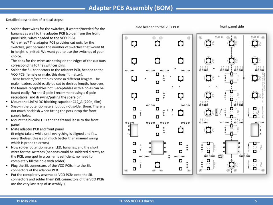
Adapter PCB Assembly (BOM)
Detailled description of critical steps:
Solder short wires for the switches, if wanted/needed for the bananas as well to the adapter PCB (solder from the front panel side, wires headed to the VCO PCB).Why wires? The adapter PCB provides cut outs for the switches, just because the number of switches that would fit in height is limited. We want you to use the switches of your choice.The pads for the wires are sitting on the edges of the cut outs corresponding to the swithces pins.
Solder the SIL connectors to the adapter PCB, headed to the VCO PCB (female or male, this doesn’t matter).These headers/receptables come in different lenghts. The male headers could easily be cut to desired length, however, the female receptables not. Receptables with 4 poles can be found easily. For the 5-pole I recommendusing a 6-pole receptable, and drawing/pulling the spare pin.
Mount the LinFM DC blocking capacitor C12_A (220n, film) Snap-in the potentiometers, but do not solder them. There is
not much backlash when fitting the pots intop the front panels holes.
Mount the bi-color LED and the fresnel lense to the front panel
Mate adapter PCB and front panel(it might take a while until everything is aligned and fits, nevertheless, this is still much better than manual wiring which is prone to errors)
Now solder potentiometers, LED, bananas, and the short wires for the switches (bananas could be soldered directly to the PCB, one spot in a corner is sufficient, no need to completely fill the hole with solder)
Plug the SIL connectors of the VCO PCBs into the SIL connectors of the adapter PCB.
Put the completely assembled VCO PCBs onto the SIL connectors and solder them (SIL connectors of the VCO PCBs are the very last step of assembly!)
front panel sideside headed to the VCO PCB