introduction to fpga and dsps joe college, chris doyle, ann marie rynning
Post on 22-Dec-2015
217 views
TRANSCRIPT
Introduction to FPGA and DSPs
Joe College, Chris Doyle,
Ann Marie Rynning
Field Programmable Gate Arrays

3
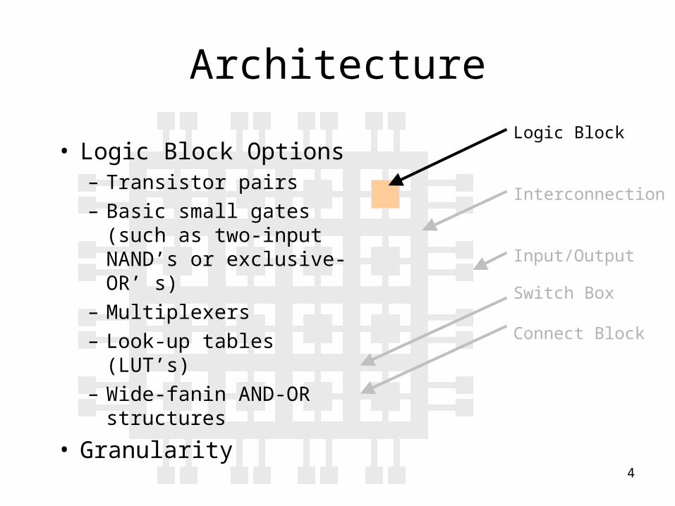
Architecture
Logic Block
Interconnection
Input/Output
Switch Box
Connect Block
4
Architecture
Logic Block
Interconnection
Input/Output
Switch Box
Connect Block
• Logic Block Options– Transistor pairs– Basic small gates (such
as two-input NAND’s or exclusive-OR’ s)
– Multiplexers– Look-up tables (LUT’s)– Wide-fanin AND-OR
structures
• Granularity

5
Architecture
Logic Block
Interconnection
Input/Output
Switch Box
Connect Block
Altera’s Stratix II ALM

6
Architecture
Logic Block
Interconnection
Input/Output
Switch Box
Connect Block
Xilink’s Virtex 4
7
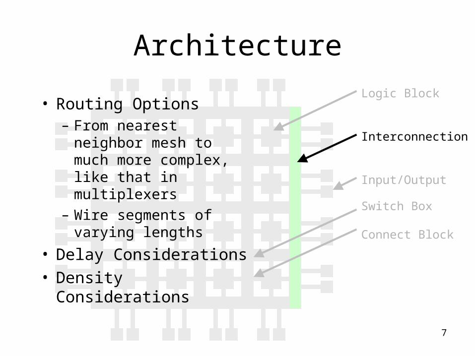
Architecture
• Routing Options– From nearest neighbor
mesh to much more complex, like that in multiplexers
– Wire segments of varying lengths
• Delay Considerations• Density Considerations
Logic Block
Interconnection
Input/Output
Switch Box
Connect Block

8
Architecture
Logic Block
Interconnection
Input/Output
Switch Box
Connect Block
• Provide programmable multiplexers signals
• Connect shorter local wires to longer-distance routing resources
9
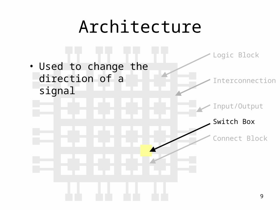
Architecture
Logic Block
Interconnection
Input/Output
Switch Box
Connect Block
• Used to change the direction of a signal
10
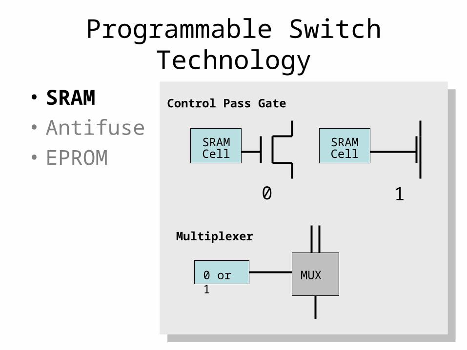
Programmable Switch Technology
• SRAM
• Antifuse
• EPROMSRAM
CellSRAM
Cell
0 1
MUX0 or 1
Control Pass Gate
Multiplexer

11
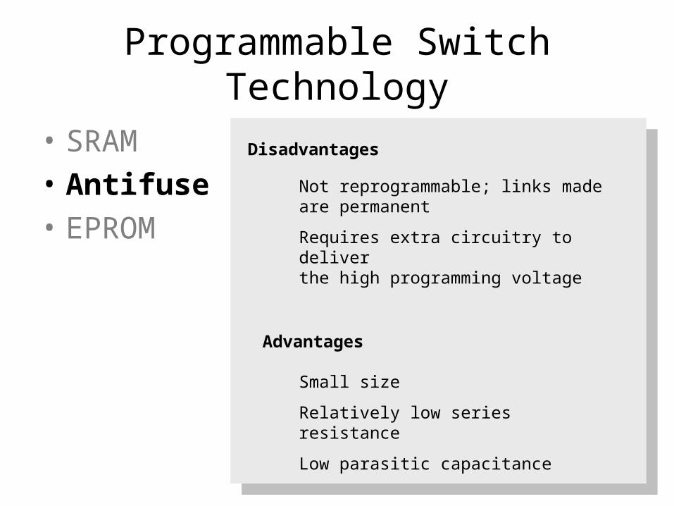
Programmable Switch Technology
• SRAM
• Antifuse
• EPROM
Disadvantages
Advantages
Volatile
External Permanent Memory Required
Large Area Required
Reprogrammable, easily and quickly
Requires only standard integrated circuit process technology (as opposed to Antifuse)

12
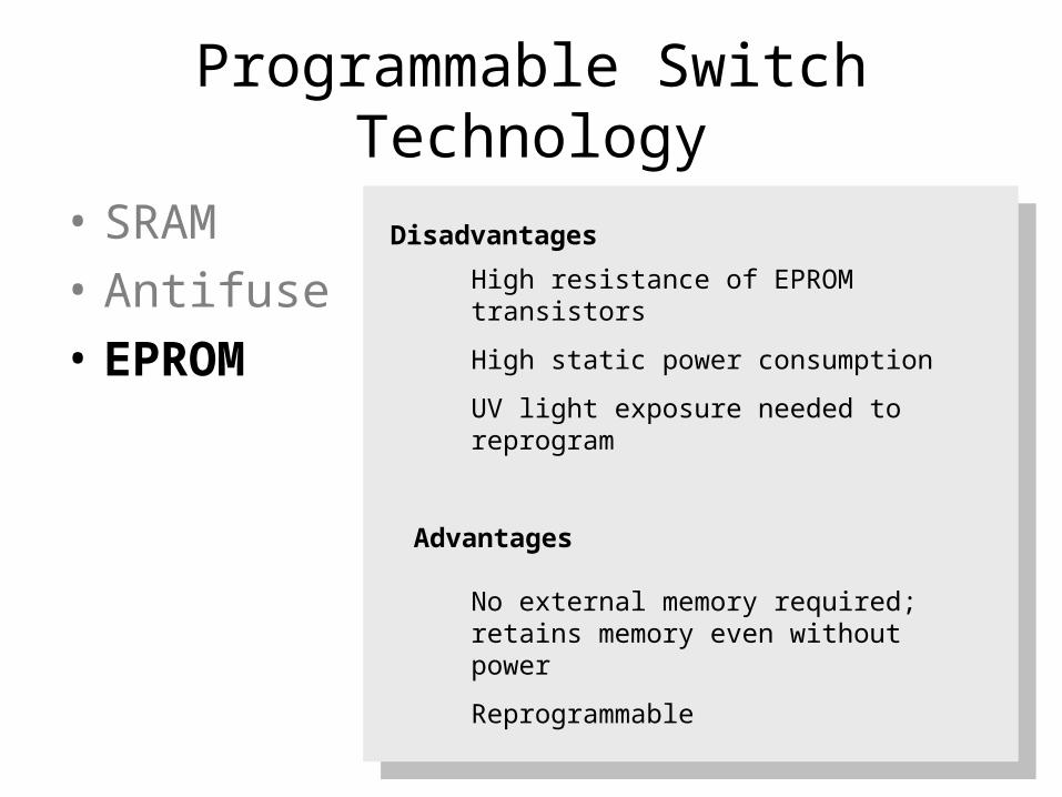
Programmable Switch Technology
• SRAM
• Antifuse
• EPROM
0
1
13
Programmable Switch Technology
• SRAM
• Antifuse
• EPROM
Disadvantages
Advantages
Not reprogrammable; links made are permanent
Requires extra circuitry to deliverthe high programming voltage
Small size
Relatively low series resistance
Low parasitic capacitance

14
Programmable Switch Technology
• SRAM
• Antifuse
• EPROM
Control Gate
Floating Gate
Bit
Line
Word Line
Drain Source
Oxide Layer
Control Gate
Floating Gate
Bit
Line
Word Line
Drain Source
Oxide Layer
1
0
- -
- - - - - - -
15
Programmable Switch Technology
• SRAM
• Antifuse
• EPROM
Disadvantages
Advantages
High resistance of EPROM transistors
High static power consumption
UV light exposure needed to reprogram
No external memory required; retains memory even without power
Reprogrammable

21
FPGA ProducersMajor Producers
Smaller Producers (specialty)

Digital Signal Processors
23
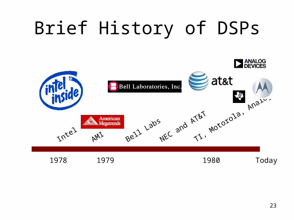
Brief History of DSPs
IntelAMI
Bell Labs
NEC and AT&T
TI, Motorola, A
nalog
1978 1979 1980 Today

25
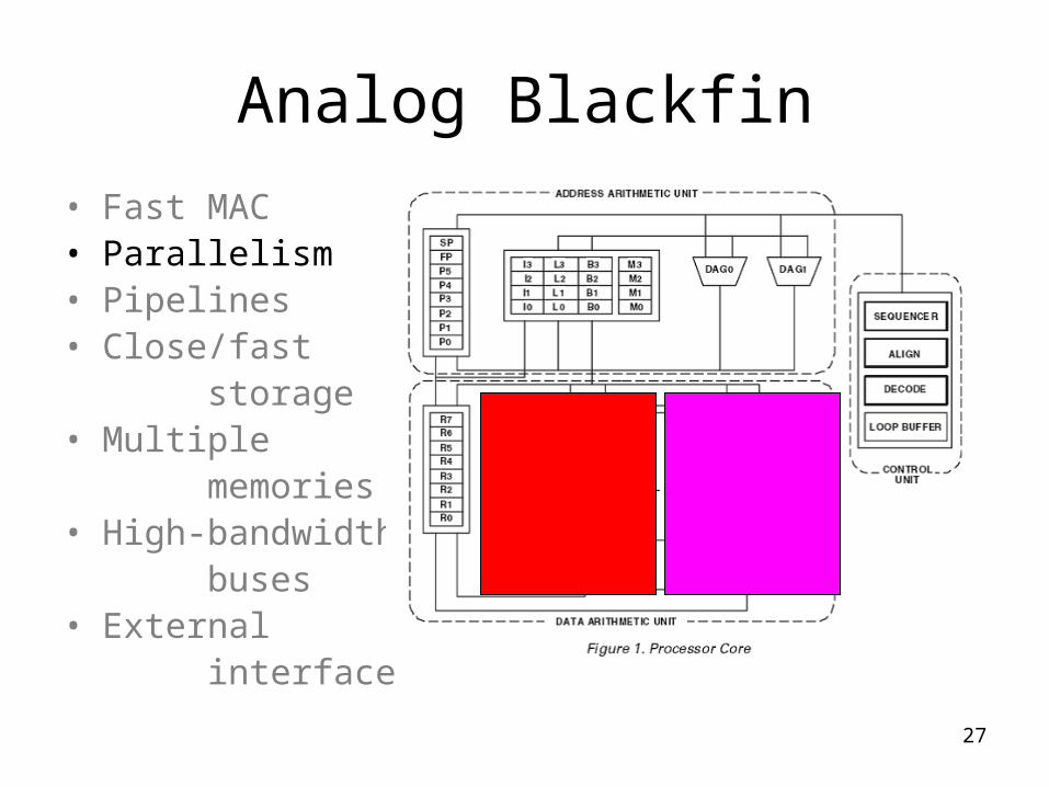
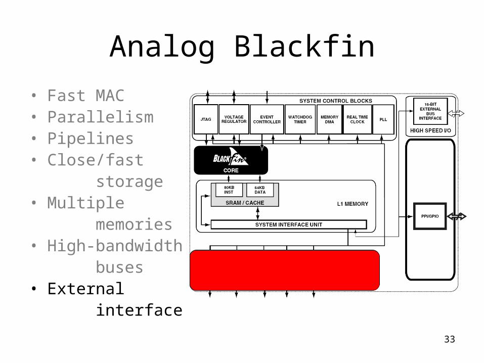
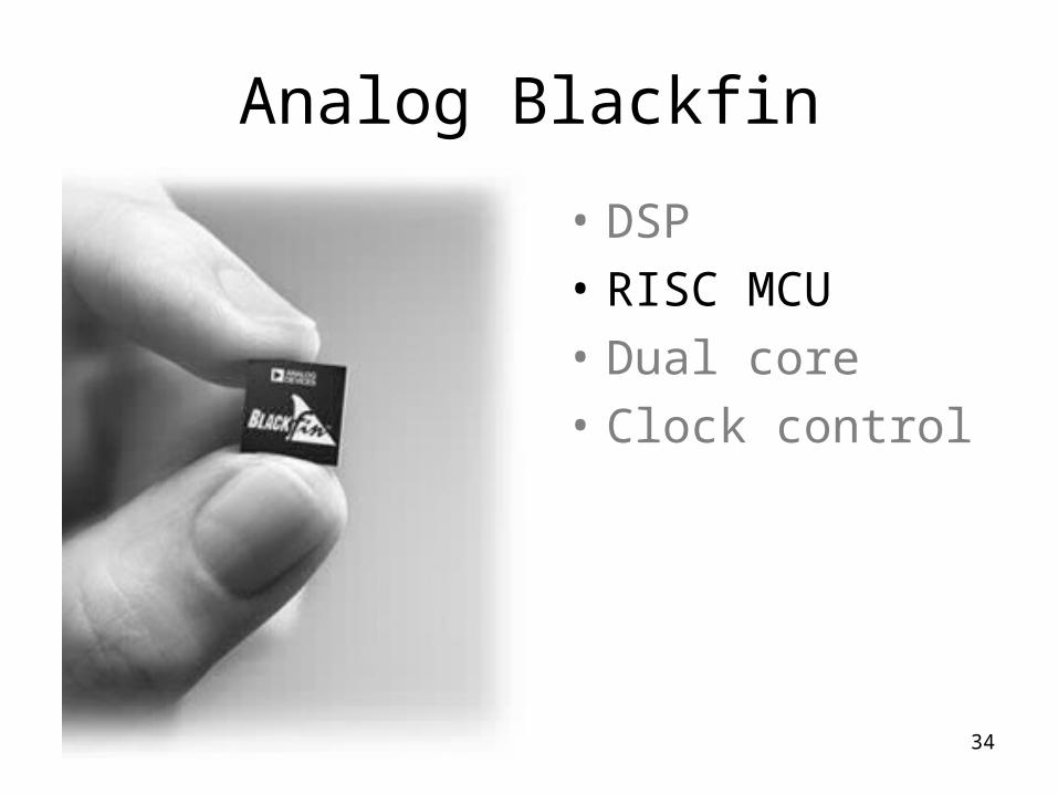
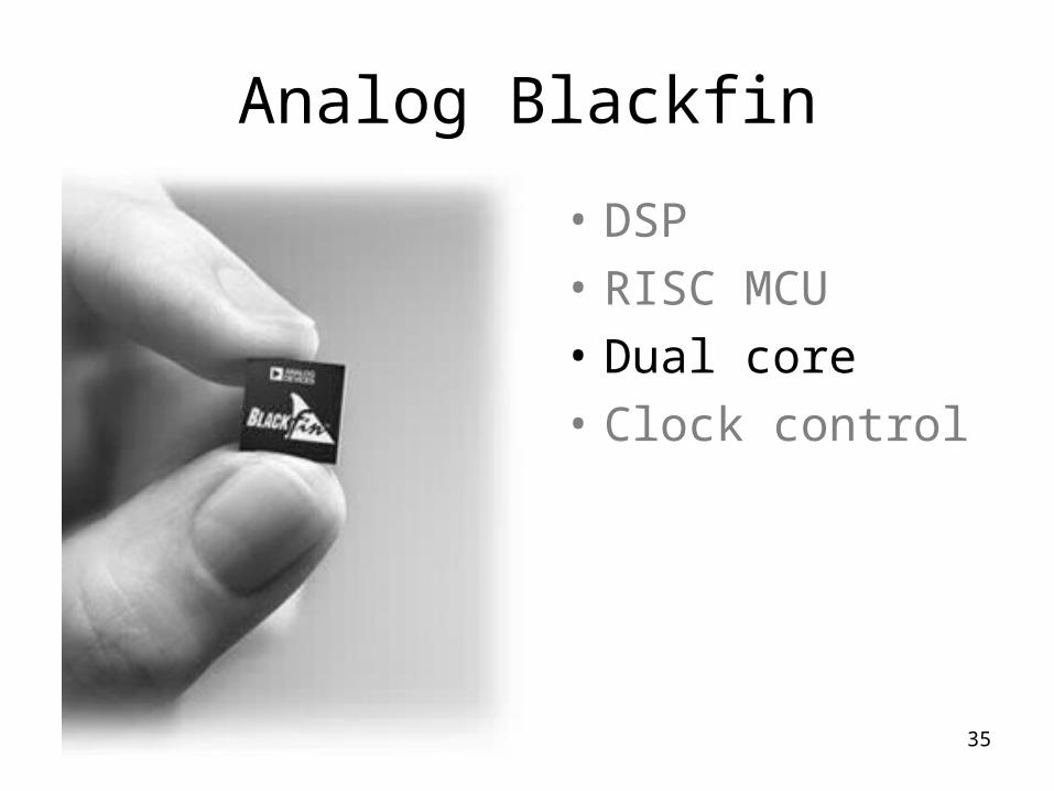
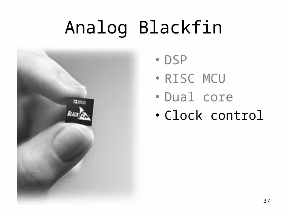
Analog Blackfin
• DSP
• RISC MCU
• Dual core
• Clock control

26
Analog Blackfin
• Fast MAC• Parallelism• Pipelines• Close/fast
storage• Multiple
memories• High-bandwidth
buses• External
interface
27
Analog Blackfin
• Fast MAC• Parallelism• Pipelines• Close/fast
storage• Multiple
memories• High-bandwidth
buses• External
interface

28
Analog Blackfin
• Fast MAC• Parallelism• Pipelines• Close/fast
storage• Multiple
memories• High-bandwidth
buses• External
interface

29
Analog Blackfin
• Fast MAC• Parallelism• Pipelines• Close/fast
storage• Multiple
memories• High-bandwidth
buses• External
interface
30
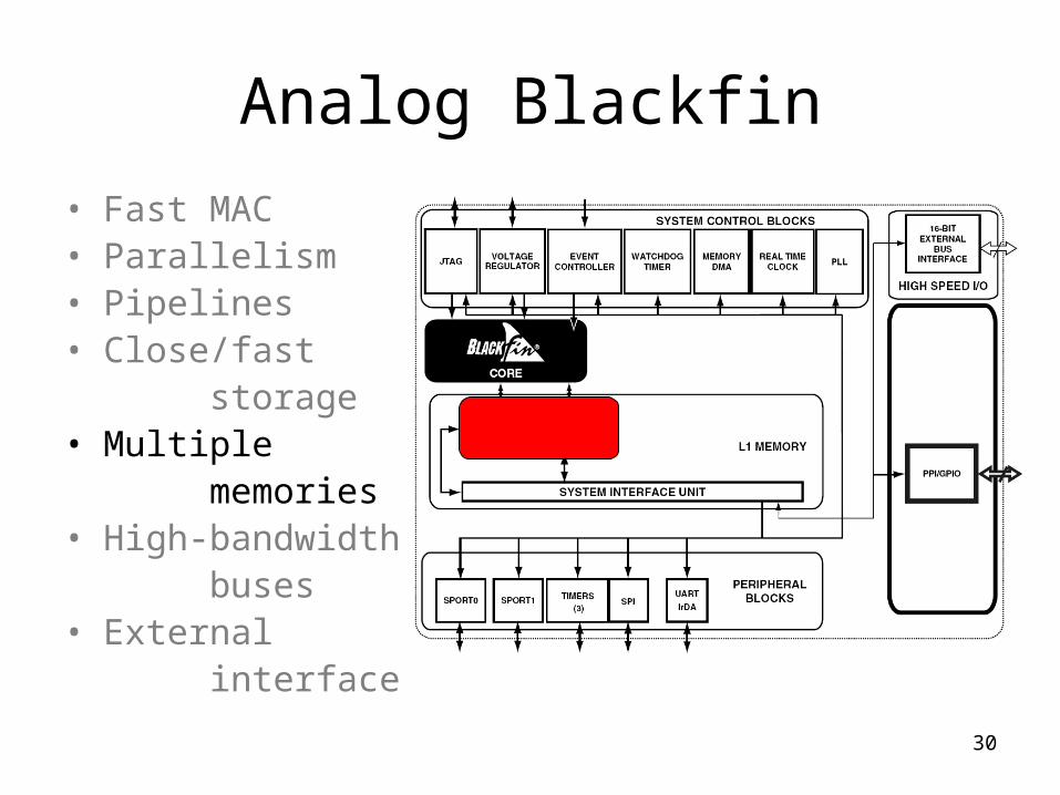
Analog Blackfin
• Fast MAC• Parallelism• Pipelines• Close/fast
storage• Multiple
memories• High-bandwidth
buses• External
interface
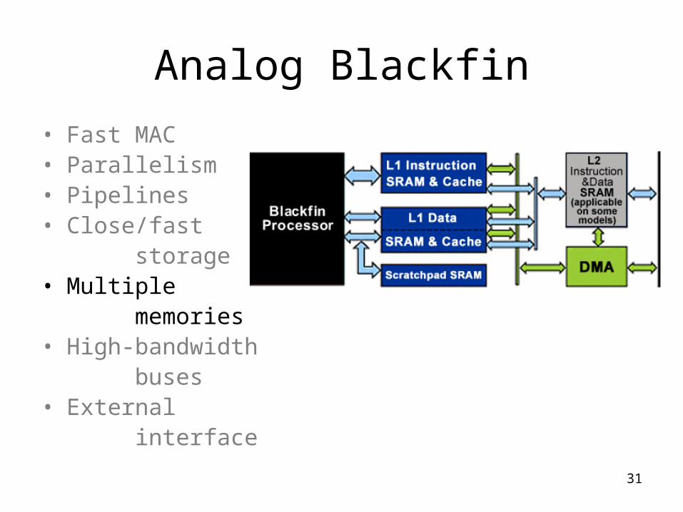
31
Analog Blackfin
• Fast MAC• Parallelism• Pipelines• Close/fast
storage• Multiple
memories• High-bandwidth
buses• External
interface

32
Analog Blackfin
• Fast MAC• Parallelism• Pipelines• Close/fast
storage• Multiple
memories• High-bandwidth
buses• External
interface
33
Analog Blackfin
• Fast MAC• Parallelism• Pipelines• Close/fast
storage• Multiple
memories• High-bandwidth
buses• External
interface
34
Analog Blackfin
• DSP
• RISC MCU
• Dual core
• Clock control
35
Analog Blackfin
• DSP
• RISC MCU
• Dual core
• Clock control

36
Analog Blackfin
37
Analog Blackfin
• DSP
• RISC MCU
• Dual core
• Clock control
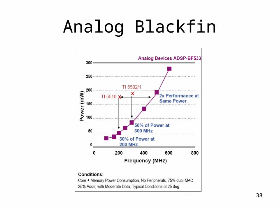
38
Analog Blackfin
42
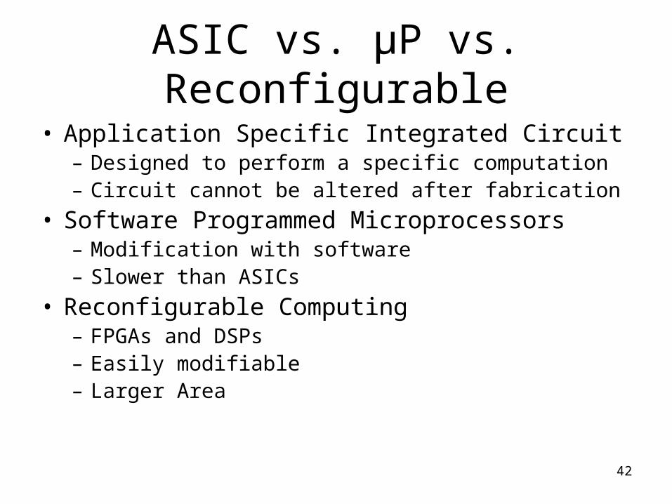
ASIC vs. µP vs. Reconfigurable
• Application Specific Integrated Circuit– Designed to perform a specific computation– Circuit cannot be altered after fabrication
• Software Programmed Microprocessors– Modification with software– Slower than ASICs
• Reconfigurable Computing– FPGAs and DSPs– Easily modifiable– Larger Area

43
Comparison
• Virtex-4 FPGA• Xilinx• 500 MHz Processor• 18-Bit MACS• 48-Bit Accumulator• Up to 1392K Bytes of
On-Chip Memory• Brand-New
• Blackfin DSP• Analog Devices• 600 MHz Processor• Two 16-Bit MACS• 40-Bit Accumulator• 308K Bytes of On-
Chip Memory• Somewhat Older
44
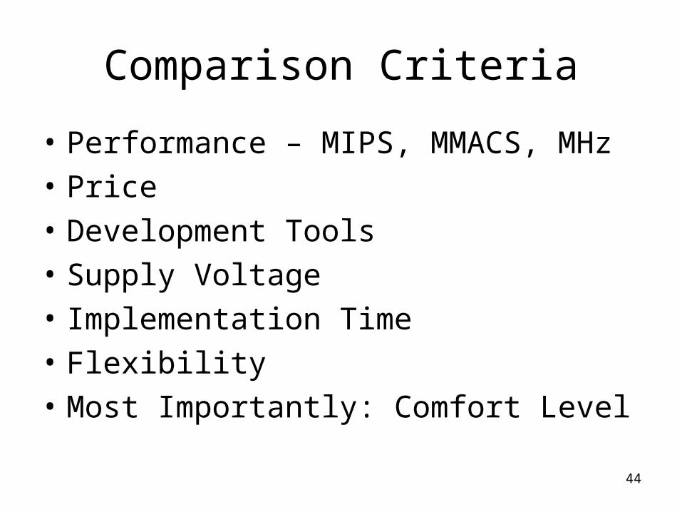
Comparison Criteria
• Performance – MIPS, MMACS, MHz
• Price
• Development Tools
• Supply Voltage
• Implementation Time
• Flexibility
• Most Importantly: Comfort Level
45
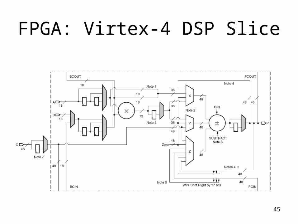
FPGA: Virtex-4 DSP Slice
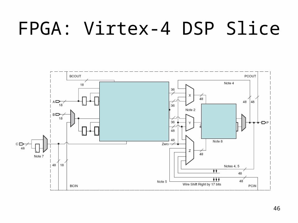
46
FPGA: Virtex-4 DSP Slice

47
DSP: Blackfin Processor Core

48
DSP: Blackfin Processor Core

49
DSP: Blackfin Processor Core
50
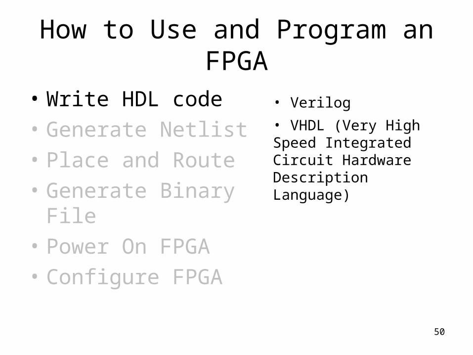
How to Use and Program an FPGA
• Write HDL code
• Generate Netlist
• Place and Route
• Generate Binary File
• Power On FPGA
• Configure FPGA
• Verilog
• VHDL (Very High Speed Integrated Circuit Hardware Description Language)
51
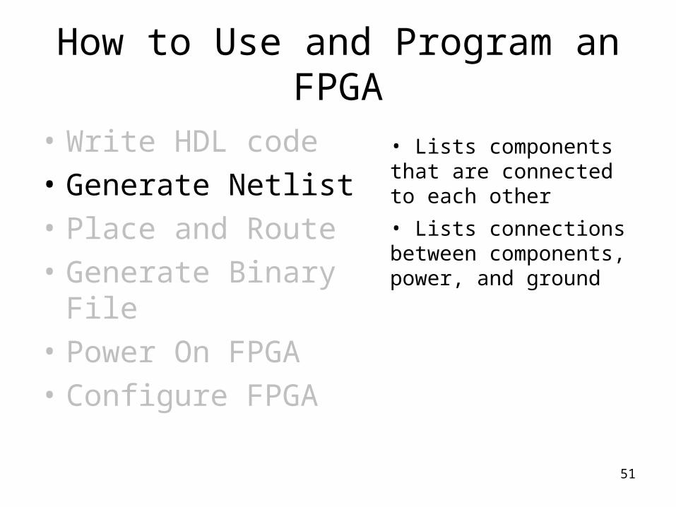
How to Use and Program an FPGA
• Write HDL code
• Generate Netlist
• Place and Route
• Generate Binary File
• Power On FPGA
• Configure FPGA
• Lists components that are connected to each other
• Lists connections between components, power, and ground
52
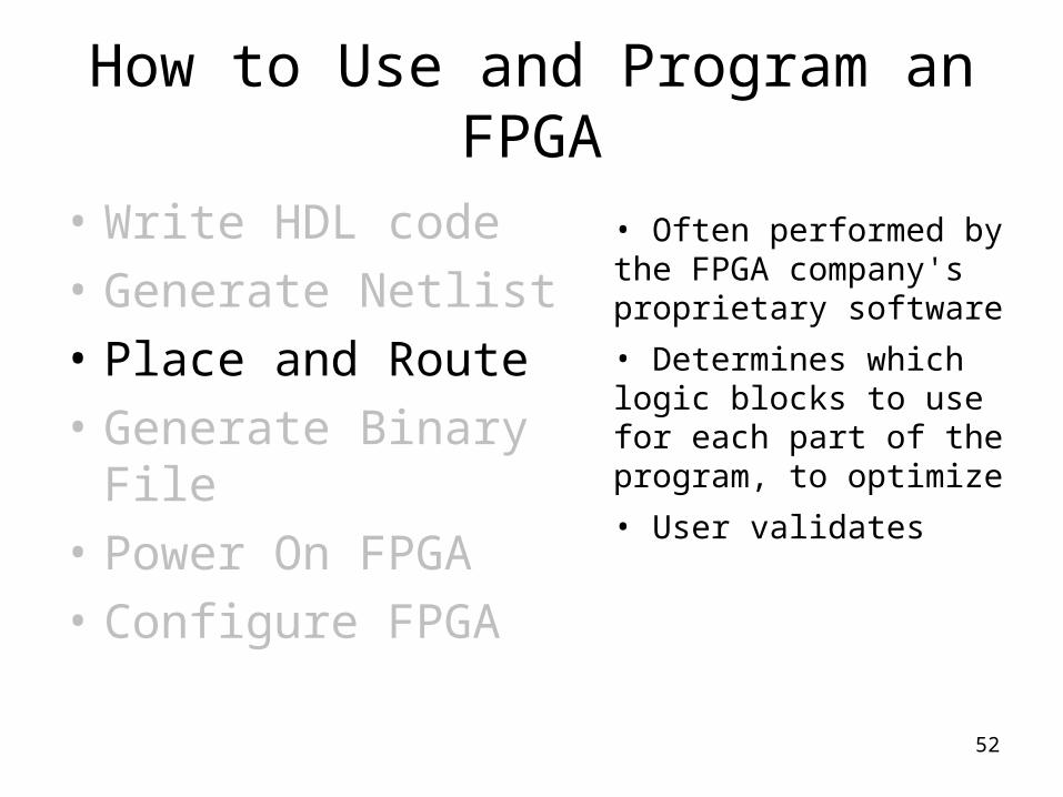
How to Use and Program an FPGA
• Write HDL code
• Generate Netlist
• Place and Route
• Generate Binary File
• Power On FPGA
• Configure FPGA
• Often performed by the FPGA company's proprietary software
• Determines which logic blocks to use for each part of the program, to optimize
• User validates

53
How to Use and Program an FPGA
• Write HDL code
• Generate Netlist
• Place and Route
• Generate Binary File
• Power On FPGA
• Configure FPGA
• Often performed by the FPGA company's proprietary software
54
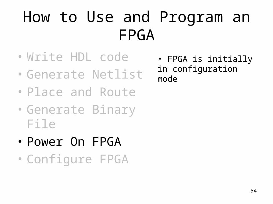
How to Use and Program an FPGA
• Write HDL code
• Generate Netlist
• Place and Route
• Generate Binary File
• Power On FPGA
• Configure FPGA
• FPGA is initially in configuration mode
55
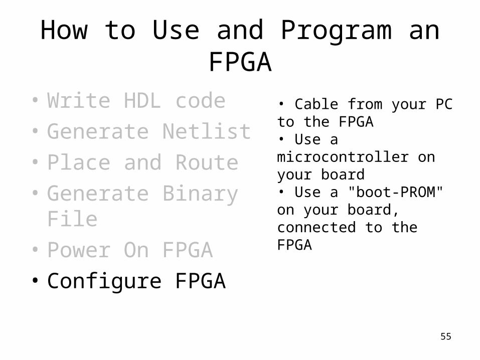
How to Use and Program an FPGA
• Write HDL code
• Generate Netlist
• Place and Route
• Generate Binary File
• Power On FPGA
• Configure FPGA
• Cable from your PC to the FPGA• Use a microcontroller on your board• Use a "boot-PROM" on your board, connected to the FPGA
56
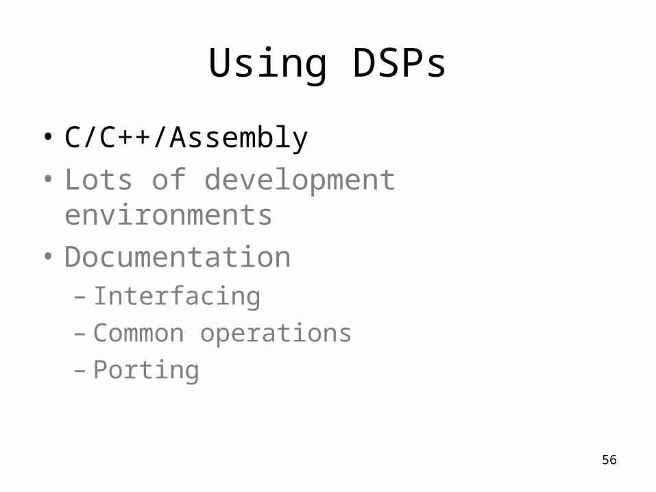
Using DSPs
• C/C++/Assembly
• Lots of development environments
• Documentation– Interfacing– Common operations– Porting
57
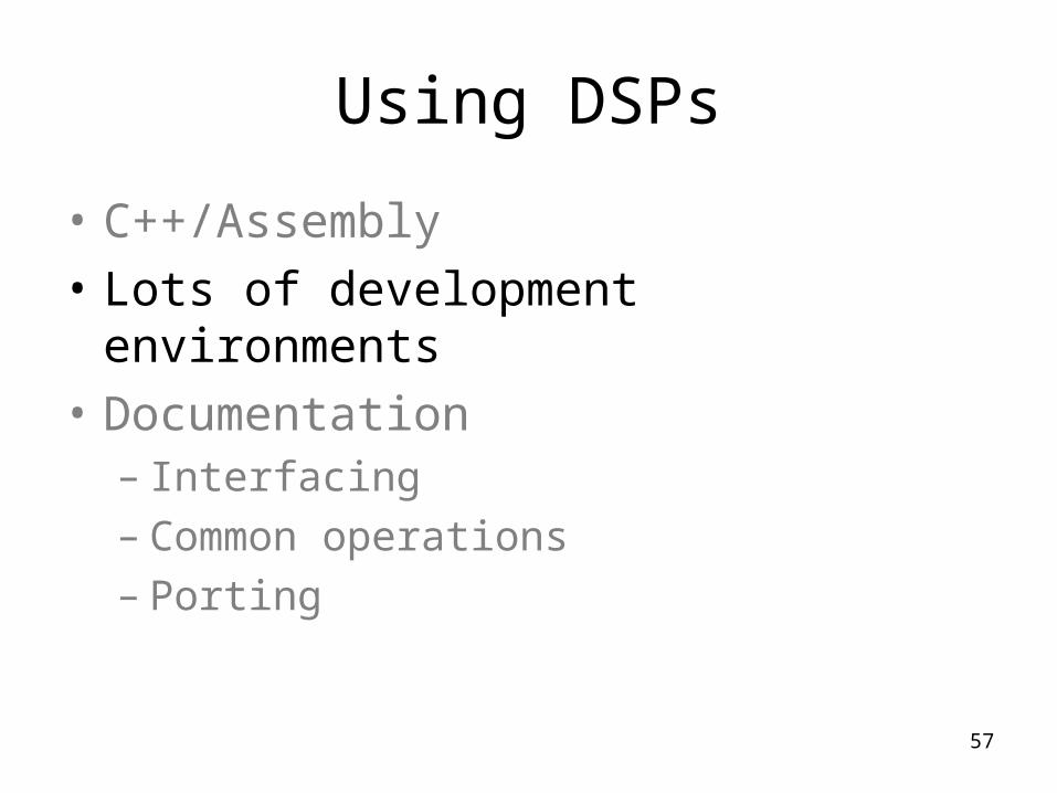
Using DSPs
• C++/Assembly
• Lots of development environments
• Documentation– Interfacing– Common operations– Porting
58
Using DSPs
• C++/Assembly
• Lots of development environments
• Documentation– Interfacing– Common operations– Porting
59
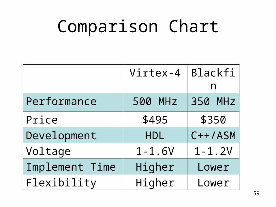
Comparison Chart
Virtex-4 Blackfin
Performance 500 MHz 350 MHz
Price $495 $350
Development HDL C++/ASM
Voltage 1-1.6V 1-1.2V
Implement Time Higher Lower
Flexibility Higher Lower