introduction to the dsp subsystem in the awr16xx edma engine consists of a channel controller (cc)...
TRANSCRIPT

1SWRA552–May 2017Submit Documentation Feedback
Copyright © 2017, Texas Instruments Incorporated
Introduction to the DSP Subsystem in the AWR16xx
Application ReportSWRA552–May 2017
Introduction to the DSP Subsystem in the AWR16xx
Sandeep Rao, Jasbir Nayyar, Mingjian Yan, Brian Johnson
ABSTRACTThis application report introduces the DSS, discusses the key blocks of the DSS, provides benchmarks forthe digital signal processor (DSP) and enhanced direct memory access (EDMA), and presents typicalradar processing chains that are intended for engineers who wish to implement signal processingalgorithms on the AWR16xx.
Contents1 Introduction ................................................................................................................... 22 Overview of the DSP Subsystem (DSS).................................................................................. 23 Algorithm Chain and Benchmarks ......................................................................................... 64 Data Flow.................................................................................................................... 105 Discussion on Cache Strategy ........................................................................................... 176 References .................................................................................................................. 18
List of Figures
1 Programmers View of the DSP Subsystem .............................................................................. 22 Memory Hierarchy in the DSS ............................................................................................. 33 Multidimensional Transfer Capabilities of the EDMA ................................................................... 44 ADC Buffers .................................................................................................................. 55 FMCW Frame Structure .................................................................................................... 76 Typical Radar Signal Processing Chain .................................................................................. 77 Variant of a Radar Signal Processing Chain............................................................................. 88 Contiguous-Read Transpose-Write EDMA Access .................................................................... 119 Transpose-Read Contiguous-Write EDMA Access .................................................................... 1210 Single-Chirp Use Case .................................................................................................... 1211 Buffer Management for Data Flow ....................................................................................... 1312 Single-Chirp Use Case Alternate Flow .................................................................................. 1413 Improving Efficiency of the Transpose Transfer ....................................................................... 1514 Timing for Multichirp Use Case........................................................................................... 1515 Multichirp Use Case ....................................................................................................... 1616 Interframe Processing Case 1............................................................................................ 1617 Interframe Processing Case 2 ............................................................................................ 17
List of Tables
1 C674x Benchmarks.......................................................................................................... 62 List of FFT Routines in DSPLIB ........................................................................................... 93 MIPS (Cycles) Performance of FFTs .................................................................................... 104 SQNR (dB) Performance of FFTs........................................................................................ 10

Introduction www.ti.com
2 SWRA552–May 2017Submit Documentation Feedback
Copyright © 2017, Texas Instruments Incorporated
Introduction to the DSP Subsystem in the AWR16xx
TrademarksC6000 is a trademark of Texas Instruments.ARM is a registered trademark of ARM Limited.Cortex is a registered trademark of ARM.All other trademarks are the property of their respective owners.
1 IntroductionThe AWR16xx device is the industry’s first fully integrated, 77-GHz, radar-on-a-chip solution forautomotive short-range radar applications [1], [2]. The device comprises the entire mmWave RF andanalog baseband signal chain for two transmitters (TX) and four receivers (RX), as well as two customer-programmable processor cores in the form of a C674x DSP and an ARM® Cortex®-R4F MCU. These twocustomer-programmable processors are part of the DSP subsystem (DSS) and master subsystem (MSS),respectively.
2 Overview of the DSP Subsystem (DSS)Figure 1 shows a programmer's view of the DSS. The center of the DSS is the C674x DSP core, whichcustomers can program to run radar signal-processing algorithms. Two levels of memory (L1 and L2) arelocal to the DSP core. Additionally, the DSP has access to external memories. These external memoriesinclude the ADC buffer (which presents the digitized radar IF signal to the DSP), the L3 memory (primarilyused to store radar data), and a handshake RAM (which can be used to share data between the MSS andthe DSS). The DSP has access to enhanced-DMA (EDMA) [6] engines, which can be used to efficientlytransport data between these external memories and the DSP core. Each of these components isdescribed in more detail in the following subsections.
Figure 1. Programmers View of the DSP Subsystem
2.1 C674x DSPThe C674x DSP [3 to 8] belongs to the C6000™ family and combines the instruction sets of two priorDSPs: C64x+ (a fixed-point DSP) and C67x (a floating-point DSP). The DSP in the AWR16xx runs at 600MHz. The DSP has the following key features:• Instruction parallelism: The CPU has eight functional units that can operate in parallel, which allows
for a maximum of eight instructions to be executed in a single cycle [3].• Rich instruction set: In addition to instruction parallelism, the DSP supports a rich instruction set [3],
which further speeds up signal processing computations. These instructions include single instructionmultiple data (SIMD) instructions, which can operate on multiple sets of input data (for example, ADD2can perform two 16-bit additions in one cycle and MAX2 can perform two 16-bit comparisons in onecycle). There are also other specialized instructions for commonly used signal-processing mathoperations (such as CMPRY, an instruction which is a single-cycle complex multiplication, specializedinstructions for dot products, and so on).

www.ti.com Overview of the DSP Subsystem (DSS)
3SWRA552–May 2017Submit Documentation Feedback
Copyright © 2017, Texas Instruments Incorporated
Introduction to the DSP Subsystem in the AWR16xx
• Optimizing C-compiler: The C6000 family of DSPs comes with a very good optimizing C compiler [5],[7], which lets engineers develop highly efficient signal-processing routines using linear C code. Thecompiler ensures optimal scheduling of instructions, to ensure the best possible use of the DSPparallelism. The compiler also supports the use of intrinsics [5], which lets the programmer directlyaccess specialized CPU instructions from within the C code.
Figure 2. Memory Hierarchy in the DSS
• Memory architecture: The DSP uses a 3-level memory architecture (L1, L2, and L3) (see Figure 2)[4].– L1 memory is the closest to the CPU and runs at the CPU speed (600 MHz). L1 memory consists
of 32KB each of program and data memory commonly referred to as L1P and L1D, respectively.– L2 memory consists of two 128KB-banks, which can store both program and data. Each bank is
accessible through its own memory port, which improves efficiency by allowing access to both L2banks simultaneously (for example, data and program simultaneously, if kept on separate banks).L2 runs at a speed of CPU/2 (300 MHz). L1 and L2 memories reside within the DSP core.
– In addition, the DSP can also access an external memory (L3). In the AWR16xx device, L3 memoryruns at 200 MHz and is accessible through a 128-bit interconnect. Both L1 and L2 memories canbe configured (partly or wholly) as cache for the next higher level memory [4]. A typical radarapplication might configure L1P and L1D as cache, place the code and data in L2, and use L3primarily for storing the radar-data (though as noted in Section 5 other variations are possible aswell).
• Collateral: Besides the optimizing C compiler, other collateral is available in the form of optimizedlibraries. The TI C6000 DSPLIB [8] is an optimized DSP function library for C programmers. The libraryincludes many C-callable, optimized, general-purpose, signal-processing routines and containsroutines for fast Fourier transforms (FFTs), matrix and vector manipulation, filtering, and more. TI alsoprovides an optimized library called the mmwaveLib [9], that complements the DSPLIB and includessignal processing routines that are commonly used in radar signal processing.
2.2 EDMAThe EDMA engine handles direct memory transfers between various memories. In the context of radarsignal processing, the amount of data to be stored per frame is typically much larger than what can beaccommodated in the higher-level memories (such as L1 and L2). Consequently, the bulk of the data isusually stored in a lower-level memory (L3). The EDMA enables data to be brought in from the lower-levelmemory to the higher-level memories for processing and subsequently shipped back to the lower-levelmemory. Proper use of the EDMA features (such as multidimensional transfers, chaining, and linking,which are explained next) can ensure that data transfers across memories occur with minimal overhead.This subsection provides a concise overview of the EDMA and its capabilities. For a more detaileddescription of the EDMA, [2], [6].
An EDMA engine consists of a channel controller (CC) and one or more transfer controllers (TCs). The CCschedules various data transfers, while the TC performs transfers dictated by requests submitted by theCC. The AWR16xx device has two CCs, each with two TCs. Because multiple TCs can operate in parallel,up to four transfers can be performed in parallel.
Overview of the DSP Subsystem (DSS) www.ti.com
4 SWRA552–May 2017Submit Documentation Feedback
Copyright © 2017, Texas Instruments Incorporated
Introduction to the DSP Subsystem in the AWR16xx
Parameters corresponding to memory transfers must be programmed into a parameter RAM (PaRAM)table. The PaRAM table is segmented into PaRAM sets. Each PaRAM set includes fields for parametersthat define a DMA transfer, such as source and destination address, transfer counts, and configurationsfor triggering, linking, chaining, and indexing. Each EDMA engine (each CC) supports 64 logical channels,and the first 64 PaRAM sets are directly mapped to the 64 logical channels.
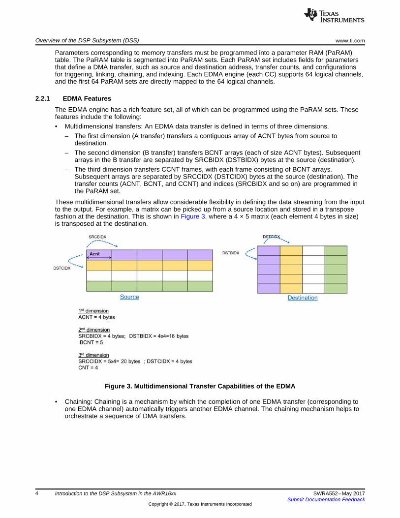
2.2.1 EDMA FeaturesThe EDMA engine has a rich feature set, all of which can be programmed using the PaRAM sets. Thesefeatures include the following:• Multidimensional transfers: An EDMA data transfer is defined in terms of three dimensions.
– The first dimension (A transfer) transfers a contiguous array of ACNT bytes from source todestination.
– The second dimension (B transfer) transfers BCNT arrays (each of size ACNT bytes). Subsequentarrays in the B transfer are separated by SRCBIDX (DSTBIDX) bytes at the source (destination).
– The third dimension transfers CCNT frames, with each frame consisting of BCNT arrays.Subsequent arrays are separated by SRCCIDX (DSTCIDX) bytes at the source (destination). Thetransfer counts (ACNT, BCNT, and CCNT) and indices (SRCBIDX and so on) are programmed inthe PaRAM set.
These multidimensional transfers allow considerable flexibility in defining the data streaming from the inputto the output. For example, a matrix can be picked up from a source location and stored in a transposefashion at the destination. This is shown in Figure 3, where a 4 × 5 matrix (each element 4 bytes in size)is transposed at the destination.
Figure 3. Multidimensional Transfer Capabilities of the EDMA
• Chaining: Chaining is a mechanism by which the completion of one EDMA transfer (corresponding toone EDMA channel) automatically triggers another EDMA channel. The chaining mechanism helps toorchestrate a sequence of DMA transfers.

www.ti.com Overview of the DSP Subsystem (DSS)
5SWRA552–May 2017Submit Documentation Feedback
Copyright © 2017, Texas Instruments Incorporated
Introduction to the DSP Subsystem in the AWR16xx
• Linking: Once the transfers corresponding to a ParRAM set have been completed (and its counterfields such as ACNT, BCNT, and CCNT have decremented to 0), the EDMA provides a mechanism toload the next PaRAM set. The 16-bit parameter LINK (in each PaRAM set [6] specifies the byteaddress offset from which the next PaRAM set should be reloaded. Once reloaded, the PaRAM set isready to be triggered again. The linking feature eliminates the need to reprogram the PaRAM set forsubsequent transfers. It is also useful in programming the EDMA so that subsequent transfersalternate between ping-pong buffers. The first 64 PaRAM sets are directly mapped to thecorresponding EDMA channels. The byte address offset programmed in LINK, is however, free to pointto a PaRAM set beyond these first 64 (the two CCs in the AWR16xx support 128 and 256 entries,respectively, in their PaRAM tables).
• Triggering: Once an EDMA channel is programmed (using the PaRAM set), it can be triggered inmultiple ways. These ways include:– Event-based triggering (for example, a chirp available interrupt from the ADC buffer, see
Section 2.3.1)– Software triggering by the DSP CPU– Chain triggering by a prior completed EDMA
The previously listed features of the EDMA are ideally suited for performing data transfers in the context ofradar signal processing. For example, radar processing involves multidimensional FFT processing, whichrequires data to be rearranged along various dimensions (range bins, Doppler bins, and antennas). Themultidimensional transfers supported by the EDMA are very useful in this context. The PaRAM set-basedprogramming model allows multiple transfers to be programmed up front. For example, EDMA transfersfrom the ADC buffer to the DSP core, and between the DSP core and the L3 memory can all beprogrammed up front in various logical channels. Subsequently, these channels are triggered during thedata flow. Further, the linking feature allows automatic reloading of PaRAM sets (for example, for eachsuccessive frame), thus eliminating the need for the CPU to periodically reprogram the EDMA channels.
2.3 External Interfaces
2.3.1 ADC BufferDigitized samples from the digital front end (DFE) are stored in the ADC buffer. The ADC buffer exists asa ping-pong pair, each 32KB in size. So when the DFE is streaming data to the ping (respectively, pong)buffer, the DSP has access to the pong (respectively, ping) buffer. The number of chirps that can bestored in a buffer is programmable. When the DSP has streamed the programmed number of chirps into abuffer, a chirp available interrupt is raised and the DFE switches buffers. This interrupt can serve as a cueto the DSP to begin processing the stored data. Alternatively, the interrupt can also be used to trigger anEDMA transfer of the ADC samples to the local memory of the DSP (such as L1 or L2), with the EDMAsubsequently interrupting the DSP on completion of the transfer. Figure 4 (left side) shows an ADC bufferthat has been programmed to store one chirp per ping-pong. The four colored rows refer to the ADCsamples corresponding to the four antennas (the four RX channels). In Figure 4 (right side), the ADCbuffer has been programmed to store four chirps per ping-pong. The data for each antenna (across thefour chirps) is stored contiguously.
Figure 4. ADC Buffers

Algorithm Chain and Benchmarks www.ti.com
6 SWRA552–May 2017Submit Documentation Feedback
Copyright © 2017, Texas Instruments Incorporated
Introduction to the DSP Subsystem in the AWR16xx
2.3.2 L3 MemoryIn the AWR16xx device, up to 768KB of the L3 memory is available for use by the DSP. The primary useof the L3 memory is to store the radar-data arising from the ADC samples corresponding to a frame(radar-cube). L3 memory can be accessed using a 128-bit interconnect.
2.3.3 Handshake MemoryAn additional 32KB of memory is available at the same hierarchy level as that of L3 memory. The primaryintent a separate memory is to have another memory for sharing the data with other masters, such asmaster R4F or DMA in the MSS, without interfering with the L3 memory access efficiency. One prime usecan be to share the final object list with the master R4F through this RAM.
3 Algorithm Chain and BenchmarksThis section provides benchmarks for some common radar signal-processing routines. This section alsoexamines the DSP loading in the context of some typical processing chains.
3.1 BenchmarksThese benchmarks assume the data and program to be in L1.
Table 1. C674x Benchmarks
Cycles Timing (µs) at 600 MHz Source and Function Name128-point FFT (16 bit) 516 0.86 µs DSPLIB (DSP_fft16x16)256-point FFT (16 bit) 932 1.55 µs DSPLIB (DSP_fft16x16)128-point FFT (32 bit) 956 1.59 µs DSPLIB (DSP_fft32x32)Windowing (16 bit) 0.595 N + 70 0.37 µs (for N = 256) mmwavelib (mmwavelib_windowing16x16)Windowing (32 bit) N + 67 0.32 µs (for N = 128) mmwavelib (mmwavelib_windowing16x32)Log2abs (16 bit) 1.8 N + 75 0.89 µs (for N = 256) mmwavelib (mmwavelib_log2Abs16)Log2abs (32 bit) 3.5 N + 68 0.86 µs (for N = 128) mmwavelib (mmwavelib_log2Abs32)CFAR-CA detection 3 N + 161 0.91 µs mmwavelib (mmwavelib_cfarCadB)Maximum of a vector oflength 256
70 0.12 µs DSPLIB (DSP_maxval)
Sum of complex vector oflength 256 (16-bit I, Q)
169 0.28 µs –
Multiply two complex vectorsof length 256 (16-bit)
265 0.44 µs –
3.2 Radar Signal Processing ChainThe fundamental transmission unit of an FMCW radar is a frame, which consists of a number (forexample, Nchirp) of equispaced chirps (see Figure 5). Central to FMCW radar signal processing is a seriesof three FFTs commonly called the range-FFT, Doppler-FFT, and angle-FFT, which respectively resolveobjects in range, Doppler (relative velocity with regard to the radar), and angle of arrival. The range-FFT isperformed across ADC samples for each chirp (one range-FFT for each RX antenna). The range-FFT isusually performed inline (during the intraframe period as the samples corresponding to each chirp becomeavailable). The Doppler-FFT operates across chirps and can only be performed when all the range-FFTscorresponding to all the chirps in a frame have become available. Lastly, the angle-FFTs are performed onthe range-Doppler processed data across RX antennas. For more in-depth information on FMCW signalprocessing [10].

www.ti.com Algorithm Chain and Benchmarks
7SWRA552–May 2017Submit Documentation Feedback
Copyright © 2017, Texas Instruments Incorporated
Introduction to the DSP Subsystem in the AWR16xx
Figure 5. FMCW Frame Structure
Figure 6 shows a representative signal-processing chain for the FMCW radar. The processing isperformed on each frame of received data. The ADC samples corresponding to each chirp (across thefour RX antennas) are received in the ADC buffer. The DSP performs an FFT (one for each RX antenna),which is then placed in L3 memory. The data in L3 memory is best visualized as a 3-dimensional matrixindexed along range, chirps, and antennas (often called a radar-cube).
When all the range-FFTs have been computed for all the chirps in a frame, Doppler-FFTs are performed.For each range-bin (and for each antenna) a Doppler-FFT is performed across the Nchirp chirps. In theexample of Figure 6, both the range-FFT and Doppler-FFT are 16-bit FFTs. Therefore, the results of theDoppler-FFT can be stored in-place (overwriting the corresponding range-FFT samples) in the radar-cubein L3 memory. At the end of the Doppler-FFT processing, the radar-cube is now indexed along range,Doppler, and antennas.
Next the radar-cube is noncoherently summed along the antenna dimension to create a predetectionmatrix that is indexed along range and Doppler. This predetection matrix is much smaller than the radar-cube. In the previous example, the predetection matrix would be 1/8 the size of the radar-cube. Thereduction is due to collapsing along the antenna dimension contributing a factor of ¼, and the fact that thepredetection matrix is real, while the radar-cube is complex contributing a factor of 1/2. Consequently, thepredetection matrix can be stored in either L3 or L2. A detection algorithm then identifies peaks in thispredetection matrix that correspond to valid objects. For each valid object, an angle-FFT is then performedon the corresponding range-Doppler bins in the radar-cube to identify the angle of arrival of that object.
Lastly, the estimated parameters for the detected objects such as range, Doppler, and angle of arrival canbe shared with the MSS using the handshake memory. There is also an option to perform furtherprocessing such as clustering and tracking in the DSP. Alternatively, these higher-layer algorithms can beperformed in the MSS (R4F MCU).
Figure 6. Typical Radar Signal Processing Chain
Algorithm Chain and Benchmarks www.ti.com
8 SWRA552–May 2017Submit Documentation Feedback
Copyright © 2017, Texas Instruments Incorporated
Introduction to the DSP Subsystem in the AWR16xx
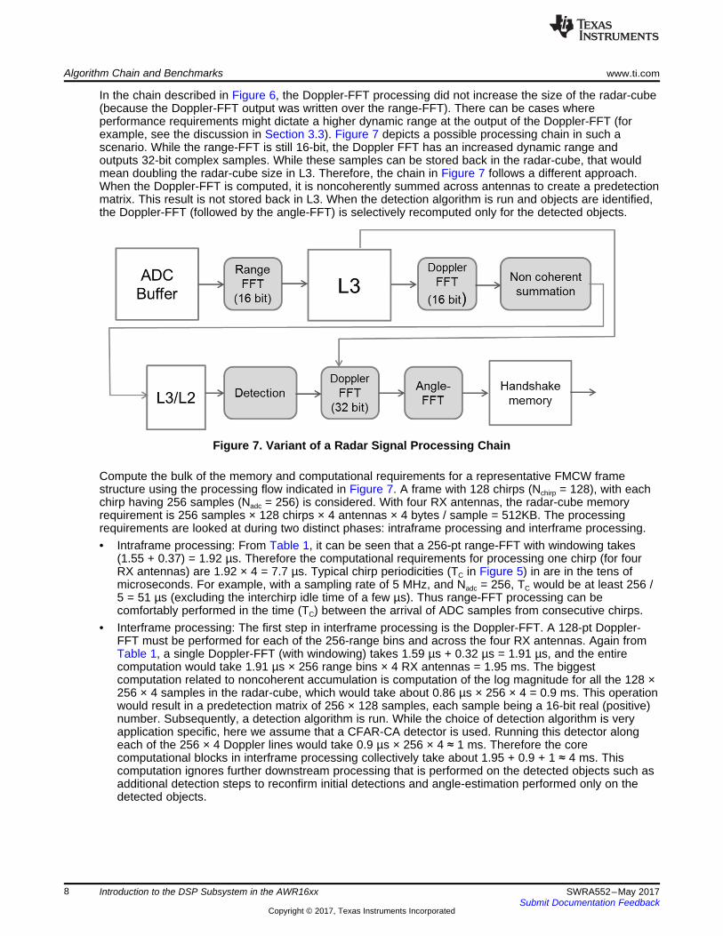
In the chain described in Figure 6, the Doppler-FFT processing did not increase the size of the radar-cube(because the Doppler-FFT output was written over the range-FFT). There can be cases whereperformance requirements might dictate a higher dynamic range at the output of the Doppler-FFT (forexample, see the discussion in Section 3.3). Figure 7 depicts a possible processing chain in such ascenario. While the range-FFT is still 16-bit, the Doppler FFT has an increased dynamic range andoutputs 32-bit complex samples. While these samples can be stored back in the radar-cube, that wouldmean doubling the radar-cube size in L3. Therefore, the chain in Figure 7 follows a different approach.When the Doppler-FFT is computed, it is noncoherently summed across antennas to create a predetectionmatrix. This result is not stored back in L3. When the detection algorithm is run and objects are identified,the Doppler-FFT (followed by the angle-FFT) is selectively recomputed only for the detected objects.
Figure 7. Variant of a Radar Signal Processing Chain
Compute the bulk of the memory and computational requirements for a representative FMCW framestructure using the processing flow indicated in Figure 7. A frame with 128 chirps (Nchirp = 128), with eachchirp having 256 samples (Nadc = 256) is considered. With four RX antennas, the radar-cube memoryrequirement is 256 samples × 128 chirps × 4 antennas × 4 bytes / sample = 512KB. The processingrequirements are looked at during two distinct phases: intraframe processing and interframe processing.• Intraframe processing: From Table 1, it can be seen that a 256-pt range-FFT with windowing takes
(1.55 + 0.37) = 1.92 µs. Therefore the computational requirements for processing one chirp (for fourRX antennas) are 1.92 × 4 = 7.7 µs. Typical chirp periodicities (TC in Figure 5) in are in the tens ofmicroseconds. For example, with a sampling rate of 5 MHz, and Nadc = 256, TC would be at least 256 /5 = 51 µs (excluding the interchirp idle time of a few µs). Thus range-FFT processing can becomfortably performed in the time (TC) between the arrival of ADC samples from consecutive chirps.
• Interframe processing: The first step in interframe processing is the Doppler-FFT. A 128-pt Doppler-FFT must be performed for each of the 256-range bins and across the four RX antennas. Again fromTable 1, a single Doppler-FFT (with windowing) takes 1.59 µs + 0.32 µs = 1.91 µs, and the entirecomputation would take 1.91 µs × 256 range bins × 4 RX antennas = 1.95 ms. The biggestcomputation related to noncoherent accumulation is computation of the log magnitude for all the 128 ×256 × 4 samples in the radar-cube, which would take about 0.86 µs × 256 × 4 = 0.9 ms. This operationwould result in a predetection matrix of 256 × 128 samples, each sample being a 16-bit real (positive)number. Subsequently, a detection algorithm is run. While the choice of detection algorithm is veryapplication specific, here we assume that a CFAR-CA detector is used. Running this detector alongeach of the 256 × 4 Doppler lines would take 0.9 µs × 256 × 4 ≈ 1 ms. Therefore the corecomputational blocks in interframe processing collectively take about 1.95 + 0.9 + 1 ≈ 4 ms. Thiscomputation ignores further downstream processing that is performed on the detected objects such asadditional detection steps to reconfirm initial detections and angle-estimation performed only on thedetected objects.

www.ti.com Algorithm Chain and Benchmarks
9SWRA552–May 2017Submit Documentation Feedback
Copyright © 2017, Texas Instruments Incorporated
Introduction to the DSP Subsystem in the AWR16xx
In the processing chains discussed so far, the low-level processing chain (up to the angle-FFT) usedfixed-point arithmetic. (Subsequent higher-layer processing (such as clustering and tracking) is typicallydone in floating point.) However, it is also possible to construct a MIPS-efficient chain where all theprocessing starting from the Doppler-FFT is in floating point as explained below.
C674x DSP provides a set of floating-point instructions that can accomplish addition, subtraction,multiplication and conversion between 32-bit fixed point and floating point, in single cycle for single-precision floating point, and in one to two cycles for double precision floating-point. There are also fastinstructions to calculate reciprocal and reciprocal square root in single cycle with 8-bit precision. With onea more iterations of Newton-Raphson interpolation, one can achieve higher precision in 10 to couple of10s of cycles. Table 3 indicates that a floating-point FFT is almost as efficient as a 32-bit fixed-point FFT.Another advantage of using floating-point arithmetic is that users can maintain both precision and dynamicrange of the input and output signal without spending cycles rescaling intermediate computation results,and enable them to skip or do less requalification of the fixed-point implementation of an algorithm, whichmakes algorithm porting easier and faster.
3.3 FFT PerformanceFFT processing forms a significant part of the lower-level radar signal processing in the FMCW radar. Theoptimized DSP library (DSPLIB) has efficient FFT routines (both fixed and floating point variants) that havebeen specifically optimized for the C674x DSP. The fastest routine is the DSP_fft16x16() which takes 0.86µs (128-point FFT) and 1.55 µs (256-point FFT) on a C674x running at 600 MHz. It operates on a 16-bitcomplex input to produce a 16-bit complex output. It accesses a precomputed twiddle factor table, whichis also stored as 16-bit complex numbers. This FFT uses multiple radix-4 butterfly stages, with the laststage being either a radix-2 or radix-4 depending on whether the FFT length is an odd or even power of 2.Every radix-4 stage (except the last stage) has a scaling by 2. There is no scaling in the last stage. Sothere is a bit growth (worst case) of 1 in every (radix-4) stage preceding the last stage. The last stage hasa bit growth of 1 or 2 depending on whether it is a radix-2 or radix-4. Thus, for a 128-point FFT, thisroutine has a bit growth of 4 (1 + 1 + 1 + 1) and can handle a 12-bit signed input with no clipping, resulting(for tone at the input) in a full-scale peak at the FFT output.
In most radar applications, the 16 × 16 FFT routines previously described suffices for the first dimension(range) processing. However, subsequent FFT processing stages could involve bit growth that extendsbeyond 16 bits. The use of 32-bit FFT routines available in DSPLIB allows these subsequent stages torealize their full processing gain without being limited by either bit overflow or the quantization noise of theFFT routine. As an example, DSP_fft32x32() works on 32-bit complex inputs producing 32-bit complexoutputs, and uses a precomputed twiddle factor table also stored as 32-bit complex numbers.
A list of some key FFT routines available with DSPLIB is provided in Table 2. Additionally, the mmwavelibrary [9] also has some useful associated routines such as windowing.
Table 2. List of FFT Routines in DSPLIB
Function Name DescriptionDSP_fft16x16 Fixed-point FFT using 16-bit complex numbers for input and output (16-bit I and 16-bit Q). The
twiddle factor table is also stored as 16-bit complex. There is a scaling by 2 after every radix-4 stage(except the last stage which can be either a radix 4 or a radix 2). The minimum length of the FFT is16. All buffers are assumed to be 8-byte aligned. The FFT works for input lengths which are powersof 2 or 4.
DSP_fft16x32 Fixed-point FFT using 16-bit complex numbers for input and output (16-bit I and 16-bit Q). Thetwiddle factor table is stored as 32-bit complex. There is a scaling by 2 after every radix-4 stage(except the last stage which can be either a radix 4 or a radix 2). The minimum length of the FFT is16. All buffers are assumed to be 8-byte aligned. The FFT works for input lengths which are powersof 2 or 4.
DSP_fft32x32 Fixed-point FFT using 32-bit complex numbers for input and output (32-bit I and 32-bit Q). Thetwiddle factor table is also stored as 32-bit complex. There is no scaling in this FFT. The minimumlength of the FFT is 16. All buffers are assumed to be 8-byte aligned. The FFT works for inputlengths which are powers of 2 or 4.
DSPF_sp_fftSPxSP This FFT uses complex floating-point input and output. The twiddle factors are also in floating point.There is no scaling in this FFT. The minimum length of the FFT is 16. All buffers are assumed to be8-byte aligned. The FFT works for input lengths which are powers of 2 or 4.

Data Flow www.ti.com
10 SWRA552–May 2017Submit Documentation Feedback
Copyright © 2017, Texas Instruments Incorporated
Introduction to the DSP Subsystem in the AWR16xx
Table 3 lists the cycle count for these FFT routines.
Table 3. MIPS (Cycles) Performance of FFTs
FunctionName N = 32 N = 64 N = 128 N = 256 N = 512 N = 1024 N = 2048DSP_fft16x16 160 240 516 932 2168 4216 9868DSP_fft16x32 241 369 816 1488 3503 6831 16078DSP_fft32x32 261 413 956 1772 4267 8363 19914DSPF_sp_fftSPxSP
305 473 1066 1962 4683 9163 21740
Ideally, users would like to ensure that the quantization noise coming from the FFT processing does notlimit the output SNR. Table 4 lists the SQNR performance metrics (in dBFS) for various FFT routines. Forinput data with effective bit widths of B bits, the SNR at the input is Bx6 + 1.76 dB. The ideal SNR after anN point first dimension FFT is Bx6 + 1.76 + 10log10(N). If B = 10 bits and N = 128, the ideal output SNR isless than 83 dB. Consequently, the use of DSP_fft16x16 (which, from Table 4, has an SQNR of 85 dB)will not limit the output SNR. Similarly, depending on the input SNR and the FFT length, other optionssuch as DSP_fft32x32() can be considered. For optimal performance the input back off should beappropriately chosen to prevent clipping at the output.
Table 4. SQNR (dB) Performance of FFTs
FunctionName N = 32 N = 64 N = 128 N = 256 N = 512 N = 1024 N = 2048DSP_fft16x16 89 87.5 88.3 85.3 87 84.2 86.3DSP_fft16x32 101.3 105.4 104.4 108.7 108.7 112.7 113.4DSP_fft32x32 175.7 173 169.9 167 164.1 161.2 158.2
The 32-bit FFT routine provides additional space for bit-width growth. A useful technique when using thisroutine is to left shift/scale the input by a few bits. The free lower bits thus obtained ensure that thequantization noise of subsequent FFT stages does not limit the processing gain.
4 Data FlowWhile Section 3 focused on algorithmic benchmarks, this section focuses on data flows. A typical radarsignal-processing chain requires data transfer from the ADC buffer to the DSP local memory (L1 or L2),and to and fro between the DSP local memory and L3. These data transfers are primarily accomplishedusing the EDMA. It is important to understand the various types of EDMA transfers and their associatedlatencies. This will enable the stitching together of a data flow that has minimal overhead and is asnonintrusive as possible.
4.1 Types of EDMA TransfersThree kinds of EDMA transfers are relevant in the context of FMCW radar signal processing.• Contiguous-Read Contiguous-Write (or contiguous): This is the simplest and fastest kind of data
transfer, which involves moving a portion of memory from a source to a destination with no datarearrangement involved during the transfer. This transfer is accomplished as a single-dimensionaltransfer (with ACNT specifying the number of bytes to be transferred). The speed of this transfer is 128bits per cycle (at 200 MHz). In a typical radar signal-processing chain where each data element is a32-bit complex number (16-bit I and 16-bit Q), this amounts to four samples being transferred in everycycle. Thus a transfer of 256 complex samples would take about 0.32 µs. The transfer of data from theADC buffer to the L2 memory of the DSPs before range-FFT processing would be an example of acontiguous transfer.
www.ti.com Data Flow
11SWRA552–May 2017Submit Documentation Feedback
Copyright © 2017, Texas Instruments Incorporated
Introduction to the DSP Subsystem in the AWR16xx
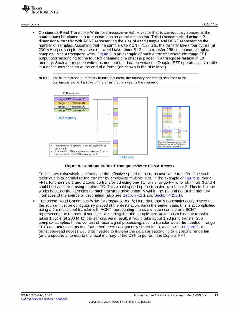
• Contiguous-Read Transpose-Write (or transpose-write): A vector that is contiguously spaced at thesource must be placed in a transpose fashion at the destination. This is accomplished using a 2-dimensional transfer with ACNT representing the size of each sample and BCNT representing thenumber of samples. Assuming that the sample size ACNT <128 bits, the transfer takes four cycles (at200 MHz) per sample. As a result, it would take about 5.12 µs to transfer 256-contiguous complexsamples using a transpose-write. Figure 8 is an example of such a transfer where the range-FFToutput (corresponding to the four RX channels of a chirp) is placed in a transpose fashion in L3memory. Such a transpose-write ensures that the data on which the Doppler-FFT operates is availablein a contiguous fashion at the end of a frame (as shown in the blue inset).
NOTE: For all depictions of memory in this document, the memory address is assumed to becontiguous along the rows of the array that represents the memory.
Figure 8. Contiguous-Read Transpose-Write EDMA Access
Techniques exist which can increase the effective speed of the transpose-write transfer. One suchtechnique is to parallelize the transfer by employing multiple TCs. In the example of Figure 8, range-FFTs for channels 1 and 2 could be transferred using one TC, while range-FFTs for channels 3 and 4could be transferred using another TC. This would speed up the transfer by a factor 2. This techniqueworks because the latencies for such transfers arise primarily within the TC and not at the memoryinterfaces of the source or destination (also see Section 4.2.1 and Section 4.2.1.1).
• Transpose-Read Contiguous-Write (or transpose-read): Here data that is noncontiguously placed atthe source must be contiguously placed at the destination. As in the earlier case, this is accomplishedusing a 2-dimensional transfer with ACNT representing the size of each sample and BCNTrepresenting the number of samples. Assuming that the sample size ACNT <128 bits, the transfertakes 1 cycle (at 200 MHz) per sample. As a result, it would take about 1.28 µs to transfer 256complex samples. In the context of radar signal processing, such a transfer would be needed if range-FFT data across chirps in a frame had been contiguously stored in L3, as shown in Figure 9. Atranspose-read access would be needed to transfer the data corresponding to a specific range bin(and a specific antenna) to the local memory of the DSP to perform the Doppler-FFT.

Data Flow www.ti.com
12 SWRA552–May 2017Submit Documentation Feedback
Copyright © 2017, Texas Instruments Incorporated
Introduction to the DSP Subsystem in the AWR16xx
Figure 9. Transpose-Read Contiguous-Write EDMA Access
4.2 Example Use Cases: Intraframe Processing (Range-FFT Processing)We use a few illustrative examples to demonstrate the use of the EDMA during range-FFT processing (byno means is this an exhaustive set of examples).
4.2.1 Single-Chirp Use CaseSingle chirp refers to the use case where the ADC buffer has been programmed to issue an interrupt afterdata for each chirp (across four RX channels) becomes available. The EDMA channel is programmed tointerrupt the DSP when the transfer is complete. This is a contiguous transfer and hence is fast. Forexample, transferring 256 ADC samples across four RX channels would take 256 × 4 / 4 / 200 ≈ 1.28 µs.The DSP performs range-FFT processing on the data received for the four RX antennas. The processeddata is then transferred to the radar-cube memory in L3 through an EDMA. In this example transfer fromL2 to L3 is a transpose-write and therefore is slower (by a factor of 16 compared to a contiguous transfer).The transfer of the 256 × 4 range-FFT samples would thus take about 21 µs . However, the total latencyof both these DMA transfers is still likely to be less than the chirp period TC and would not be a bottleneck(for a 5-MHz sampling rate with Nadc = 256, TC will be 51 µs). The advantage of this approach is that iteases the data transfer latencies during the Doppler-processing. Since the range-FFT output is written outin a transpose manner, the data required for a Doppler-FFT would be contiguously placed.
Figure 10. Single-Chirp Use Case

www.ti.com Data Flow
13SWRA552–May 2017Submit Documentation Feedback
Copyright © 2017, Texas Instruments Incorporated
Introduction to the DSP Subsystem in the AWR16xx
In Figure 10, the buffering scheme in the DSP L2 consists of a triad of buffers. At any time, two of thesebuffers serve as input and output buffers for range-FFT processing. So the DSP picks up the samples forthe current chirp from the designated input buffer and places the processed range-FFT data in thedesignated output buffer. The third buffer contains the range-FFT output from the previously processedchirp. This data is transferred out (using EDMA transfer C) and samples for the next chirp are got in (usingEDMA transfer A) to replace it. In this scheme, the DSP processing will not be a bottle-neck as long as thetotal latencies associated with A and C remain less than a chirp period (also see Section 4.2.1 andSection 4.2.1.1).
Figure 11 shows the buffer management using this triad of buffers.
Figure 11. Buffer Management for Data Flow
Data Flow www.ti.com
14 SWRA552–May 2017Submit Documentation Feedback
Copyright © 2017, Texas Instruments Incorporated
Introduction to the DSP Subsystem in the AWR16xx
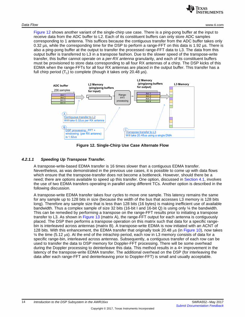
Figure 12 shows another variant of the single-chirp use case. There is a ping-pong buffer at the input toreceive data from the ADC buffer to L2. Each of its constituent buffers can only store ADC samplescorresponding to 1 antenna. This suffices because the contiguous transfer from the ADC buffer takes only0.32 µs, while the corresponding time for the DSP to perform a range-FFT on this data is 1.92 µs. There isalso a ping-pong buffer at the output to transfer the processed range-FFT data to L3. The data from thisoutput buffer is transferred to L3 in a transpose fashion. Due to the slower speed of the transpose-writetransfer, this buffer cannot operate on a per-RX antenna granularity, and each of its constituent buffersmust be provisioned to store data corresponding to all four RX antennas of a chirp. The DSP kicks of thisEDMA when the range-FFTs for all four RX antennas are placed in the output buffer. This transfer has afull chirp period (TC) to complete (though it takes only 20.48 µs).
Figure 12. Single-Chirp Use Case Alternate Flow
4.2.1.1 Speeding Up Transpose Transfer.A transpose-write-based EDMA transfer is 16 times slower than a contiguous EDMA transfer.Nevertheless, as was demonstrated in the previous use cases, it is possible to come up with data flowswhich ensure that the transpose-transfer does not become a bottleneck. However, should there be aneed; there are options available to speed up this transfer. One option, discussed in Section 4.1, involvesthe use of two EDMA transfers operating in parallel using different TCs. Another option is described in thefollowing discussion.
A transpose-write EDMA transfer takes four cycles to move one sample. This latency remains the samefor any sample up to 128 bits in size (because the width of the bus that accesses L3 memory is 128 bitslong). Therefore any sample size that is less than 128 bits (16 bytes) is making inefficient use of availablebandwidth. Thus a complex sample of size 32 bits (16-bit I and 16-bit Q) is using only ¼ the bandwidth.This can be remedied by performing a transpose on the range-FFT results prior to initiating a transposetransfer to L3. As shown in Figure 13 (matrix A), the range-FFT output for each antenna is contiguouslyplaced. The DSP then performs a transpose operation on this matrix such that data for a specific range-bin is interleaved across antennas (matrix B). A transpose-write EDMA is now initiated with an ACNT of128 bits. With this enhancement, the EDMA transfer that originally took 20.48 μs (in Figure 10), now takes¼ the time (5.12 μs). At the end of the intrachirp period, each row in L3 memory consists of data for aspecific range-bin, interleaved across antennas. Subsequently, a contiguous transfer of each row can beused to transfer the data to DSP memory for Doppler-FFT processing. There will be some overheadduring the Doppler processing to deinterleave this data. This method results in a 4× improvement in thelatency of the transpose-write EDMA transfer. The additional overhead on the DSP (for interleaving thedata after each range-FFT and deinterleaving prior to Doppler-FFT) is small and usually acceptable.

www.ti.com Data Flow
15SWRA552–May 2017Submit Documentation Feedback
Copyright © 2017, Texas Instruments Incorporated
Introduction to the DSP Subsystem in the AWR16xx
Figure 13. Improving Efficiency of the Transpose Transfer
NOTE: The DSP can transpose a 4 × 256 matrix in 576 cycles (approximately 0.96 µs).
4.2.2 Multichirp Use CaseMultichirp refers to the use case where the ADC buffer has been configured to interrupt the DSP after afixed number of chirps have been collected. Figure 14 shows the timing diagram of a multichirp use casewhere the ADC buffer interrupts the DSP after every four chirps have been collected. In contrast toFigure 5 (which depicts a single-chirp use case), note the long gaps between ADC interrupts where theDSP is not performing range-FFTs. The DSP could enter a sleep mode during these gaps in processing,making it a useful power-saving feature. Alternatively the DSP could perform higher-level processing (suchas tracking) as a background process in these gaps.
Figure 14. Timing for Multichirp Use Case
While it would be easy to adapt the techniques discussed in Section 4.2.1 to the multichirp use case, aslightly different approach is highlighted here. In the implementation shown in Figure 15, each row in theADC buffer (a single chirp for a single antenna) is transferred to L2 at a time which keeps the L2 bufferingrequirements to a minimum. The processed data from L2 is transferred to L3 as a contiguous transfer.Two ping-pong buffer pairs respectively manage the data that is input to the DSP (from the ADC buffer)and output to L3. Because both the EDMA transfers are contiguous, it ensures that the transfer latenciesdo not become a bottleneck. The latencies for both of these EDMA transfers (represented by A and C inFigure 15) is 0.32 µs, while the corresponding DSP processing latency (B) is approximately 2 µs. BecauseB > A + C, it ensures that the DSP never has to wait for an EDMA completion. In this example, the range-FFT data has been transferred to L3 without a transpose. Consequently the access for Doppler-FFT willnow involve a transpose-read EDMA access. This is an overhead that must be factored in during theDoppler-FFT processing.

Data Flow www.ti.com
16 SWRA552–May 2017Submit Documentation Feedback
Copyright © 2017, Texas Instruments Incorporated
Introduction to the DSP Subsystem in the AWR16xx
Figure 15. Multichirp Use Case
4.3 Example Use Cases: Interframe ProcessingInterframe processing primarily involves Doppler-FFT computation, detection, and angle estimation. Thedata flow is largely determined by the way the range-FFT output has been stored in L3 memory duringintraframe processing, and three such cases are discussed.• Case 1
If the range-FFT output has been placed in L3 using a transpose-write (as in for example, Figure 10)then the data required for performing a Doppler-FFT is contiguously available. This represents thesimplest scenario for interframe processing, because all L3 accesses are now through contiguousEDMA transfers. As shown in Figure 16, each line from L3 memory is transferred to the DSP localmemory (for example, L2) using a ping-pong scheme. After the Doppler-FFT has been computed, theresult can be optionally transferred back to L3 (not shown in Figure 16). During interframe processingall the required input data is available in L3. Therefore, to prevent any stalling in the processing, it isimportant that the EDMA transfer latencies keep up with the DSP-processing latencies. In the caseshown in Figure 16 (with 128 chirps), an EDMA transfer takes 0.16 µs, while a 128-pt FFT takes 0.86µs. Consequently, the EDMA transfer should not be a bottleneck even in the case where the Doppler-FFT output is written back to the radar-cube.
Figure 16. Interframe Processing Case 1
www.ti.com Discussion on Cache Strategy
17SWRA552–May 2017Submit Documentation Feedback
Copyright © 2017, Texas Instruments Incorporated
Introduction to the DSP Subsystem in the AWR16xx
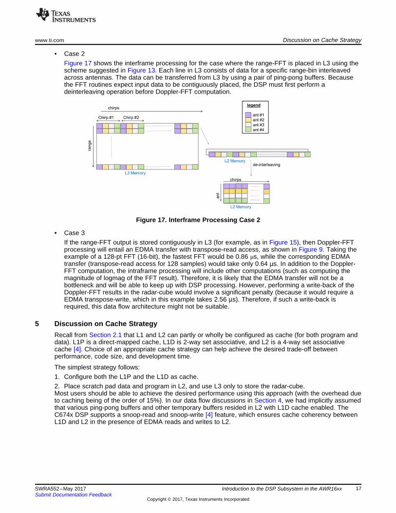
• Case 2Figure 17 shows the interframe processing for the case where the range-FFT is placed in L3 using thescheme suggested in Figure 13. Each line in L3 consists of data for a specific range-bin interleavedacross antennas. The data can be transferred from L3 by using a pair of ping-pong buffers. Becausethe FFT routines expect input data to be contiguously placed, the DSP must first perform adeinterleaving operation before Doppler-FFT computation.
Figure 17. Interframe Processing Case 2
• Case 3If the range-FFT output is stored contiguously in L3 (for example, as in Figure 15), then Doppler-FFTprocessing will entail an EDMA transfer with transpose-read access, as shown in Figure 9. Taking theexample of a 128-pt FFT (16-bit), the fastest FFT would be 0.86 μs, while the corresponding EDMAtransfer (transpose-read access for 128 samples) would take only 0.64 µs. In addition to the Doppler-FFT computation, the intraframe processing will include other computations (such as computing themagnitude of logmag of the FFT result). Therefore, it is likely that the EDMA transfer will not be abottleneck and will be able to keep up with DSP processing. However, performing a write-back of theDoppler-FFT results in the radar-cube would involve a significant penalty (because it would require aEDMA transpose-write, which in this example takes 2.56 µs). Therefore, if such a write-back isrequired, this data flow architecture might not be suitable.
5 Discussion on Cache StrategyRecall from Section 2.1 that L1 and L2 can partly or wholly be configured as cache (for both program anddata). L1P is a direct-mapped cache, L1D is 2-way set associative, and L2 is a 4-way set associativecache [4]. Choice of an appropriate cache strategy can help achieve the desired trade-off betweenperformance, code size, and development time.
The simplest strategy follows:1. Configure both the L1P and the L1D as cache.2. Place scratch pad data and program in L2, and use L3 only to store the radar-cube.Most users should be able to achieve the desired performance using this approach (with the overhead dueto caching being of the order of 15%). In our data flow discussions in Section 4, we had implicitly assumedthat various ping-pong buffers and other temporary buffers resided in L2 with L1D cache enabled. TheC674x DSP supports a snoop-read and snoop-write [4] feature, which ensures cache coherency betweenL1D and L2 in the presence of EDMA reads and writes to L2.
References www.ti.com
18 SWRA552–May 2017Submit Documentation Feedback
Copyright © 2017, Texas Instruments Incorporated
Introduction to the DSP Subsystem in the AWR16xx
However, given the highly deterministic nature of the radar signal-processing chain, additionalimprovements can be achievable by configuring a portion of L1P and L1D as RAM. Key routines whichconstitute the bulk of the radar signal processing, such as FFT and windowing routines, can be placed inL1P, while the associated scratch pad buffers (such as some of the ping-pong buffers depicted in theearlier data-flows) can be placed in L1D. In one experiment, we put all real-time frame-work and algorithmcode (up to clustering) into 24KB L1P SRAM (leaving only 8KB for L1P cache), and saw modestimprovement of cycle performance of the chain. We also configured 16KB of L1D as data SRAM (leaving16KB for L1D cache) to hold temporary processing buffers (reused between range processing andDoppler processing). By doing so we improved the cycle performance of range processing by 5~10%. Wealso saw much less cycle fluctuation in range processing due to a decrease in L1 cache activity. Thereduced size of L1 cache did not seem to degrade the cycle performance of other algorithms whichworked out of buffers in L2. This placement of code and data in L1P and L1D also saved 40KB of L2memory, without negative impact of cycle performance of the whole chain
Alternatives to EDMA-based L3 access: The data flows discussed in Section 4 relied on the EDMA engineto access data in L3. However, in some scenarios direct access of L3 memory by the CPU might also beconsidered. Each EDMA transfer has an overhead in terms of triggering the EDMA and subsequentlyverifying its completion (either through an interrupt or polling). These overheads could swamp out thebenefits of using an EDMA for small sized transfers. Such a scenario could occur, for example, in thecontext of an FMCW frame with a small number of chirps (16 or 32) resulting in small sized Doppler-FFTs.One option is to fetch data for multiple Doppler-FFTs in every EDMA transfer. This reduces the EDMAoverhead, though at the cost of proportionally larger buffer sizes. In such cases direct access to L3 (withcaching in L1D) could be a viable alternative. In one of the experiment with size 32 Doppler-FFT's, 4 Rxantennas, and 1024 range bins, we saw direct L3 access (with L1 cache on) performed slightly fastercompared to an EDMA based approach. This also reduced the code complexity (with the elimination ofEDMA triggering/polling). We also experimented on having the pre-detection matrix inside L3 memory withdirect CPU accesses (via cache). While we observed that the detection algorithm (CFAR) had cycledegradation of about 2x (vs. the pre-detection matrix residing in L2), the freeing up of L2 memory mightmake it a worthwhile trade-off in certain cases.
Code in L3: Customers also have the option of storing program code in L3. This option is typically suitedfor placing code which would be used once per frame (in one go) rather than being executed multipletimes with the other code in an interleaved manner (the intent is to reduce the loss due to repeated codeeviction). One example is Kalman filtering or detection. While actual results will vary depending on thenature of the code, our experience running a Kalman filter from L3 shows a hit of about 2× for the firstinvocation and almost no overhead for subsequent invocations (due to the program being cached in L1P).
Whenever L3 is being directly accessed by the CPU (either for code or data), multiple caching options arepossible. One option is to cache L3 directly to L1 (L1P, L1D). Another option is to create a hierarchicalcache structure, with a small part of L2 (about 32KB) also configured as cache.
6 References1. AWR1642: 77GHz Radar-on-Chip for Short-Range Radar Applications White Paper (SPRY006)2. AWR14xx/16xx Technical Reference Manual3. TMS320C674x DSP CPU and Instruction Set4. TMS320C674x DSP Megamodule Reference Guide5. TMS320C600 Optimizing Compiler User's Guide6. TMS320C6748 Technical Reference Manual7. TMS320C6000 Programmer’s Guide8. DSPLIB: Required DSPLIB libraries that must be installed for the C674x:
• The fixed-point library for the C64x+• The floating-point library for C674x (documentation included with the installation provides APIs for
all the routines and a cycle benchmarking report)9. mmwave lib: Install the mmwave-SDK and then navigate to \packages\ti\alg\mmwavelib to view both
the documentation and code for mmwavelib.10. Introduction to mm-wave sensing: FMCW Radars

IMPORTANT NOTICE FOR TI DESIGN INFORMATION AND RESOURCES
Texas Instruments Incorporated (‘TI”) technical, application or other design advice, services or information, including, but not limited to,reference designs and materials relating to evaluation modules, (collectively, “TI Resources”) are intended to assist designers who aredeveloping applications that incorporate TI products; by downloading, accessing or using any particular TI Resource in any way, you(individually or, if you are acting on behalf of a company, your company) agree to use it solely for this purpose and subject to the terms ofthis Notice.TI’s provision of TI Resources does not expand or otherwise alter TI’s applicable published warranties or warranty disclaimers for TIproducts, and no additional obligations or liabilities arise from TI providing such TI Resources. TI reserves the right to make corrections,enhancements, improvements and other changes to its TI Resources.You understand and agree that you remain responsible for using your independent analysis, evaluation and judgment in designing yourapplications and that you have full and exclusive responsibility to assure the safety of your applications and compliance of your applications(and of all TI products used in or for your applications) with all applicable regulations, laws and other applicable requirements. Yourepresent that, with respect to your applications, you have all the necessary expertise to create and implement safeguards that (1)anticipate dangerous consequences of failures, (2) monitor failures and their consequences, and (3) lessen the likelihood of failures thatmight cause harm and take appropriate actions. You agree that prior to using or distributing any applications that include TI products, youwill thoroughly test such applications and the functionality of such TI products as used in such applications. TI has not conducted anytesting other than that specifically described in the published documentation for a particular TI Resource.You are authorized to use, copy and modify any individual TI Resource only in connection with the development of applications that includethe TI product(s) identified in such TI Resource. NO OTHER LICENSE, EXPRESS OR IMPLIED, BY ESTOPPEL OR OTHERWISE TOANY OTHER TI INTELLECTUAL PROPERTY RIGHT, AND NO LICENSE TO ANY TECHNOLOGY OR INTELLECTUAL PROPERTYRIGHT OF TI OR ANY THIRD PARTY IS GRANTED HEREIN, including but not limited to any patent right, copyright, mask work right, orother intellectual property right relating to any combination, machine, or process in which TI products or services are used. Informationregarding or referencing third-party products or services does not constitute a license to use such products or services, or a warranty orendorsement thereof. Use of TI Resources may require a license from a third party under the patents or other intellectual property of thethird party, or a license from TI under the patents or other intellectual property of TI.TI RESOURCES ARE PROVIDED “AS IS” AND WITH ALL FAULTS. TI DISCLAIMS ALL OTHER WARRANTIES ORREPRESENTATIONS, EXPRESS OR IMPLIED, REGARDING TI RESOURCES OR USE THEREOF, INCLUDING BUT NOT LIMITED TOACCURACY OR COMPLETENESS, TITLE, ANY EPIDEMIC FAILURE WARRANTY AND ANY IMPLIED WARRANTIES OFMERCHANTABILITY, FITNESS FOR A PARTICULAR PURPOSE, AND NON-INFRINGEMENT OF ANY THIRD PARTY INTELLECTUALPROPERTY RIGHTS.TI SHALL NOT BE LIABLE FOR AND SHALL NOT DEFEND OR INDEMNIFY YOU AGAINST ANY CLAIM, INCLUDING BUT NOTLIMITED TO ANY INFRINGEMENT CLAIM THAT RELATES TO OR IS BASED ON ANY COMBINATION OF PRODUCTS EVEN IFDESCRIBED IN TI RESOURCES OR OTHERWISE. IN NO EVENT SHALL TI BE LIABLE FOR ANY ACTUAL, DIRECT, SPECIAL,COLLATERAL, INDIRECT, PUNITIVE, INCIDENTAL, CONSEQUENTIAL OR EXEMPLARY DAMAGES IN CONNECTION WITH ORARISING OUT OF TI RESOURCES OR USE THEREOF, AND REGARDLESS OF WHETHER TI HAS BEEN ADVISED OF THEPOSSIBILITY OF SUCH DAMAGES.You agree to fully indemnify TI and its representatives against any damages, costs, losses, and/or liabilities arising out of your non-compliance with the terms and provisions of this Notice.This Notice applies to TI Resources. Additional terms apply to the use and purchase of certain types of materials, TI products and services.These include; without limitation, TI’s standard terms for semiconductor products http://www.ti.com/sc/docs/stdterms.htm), evaluationmodules, and samples (http://www.ti.com/sc/docs/sampterms.htm).
Mailing Address: Texas Instruments, Post Office Box 655303, Dallas, Texas 75265Copyright © 2017, Texas Instruments Incorporated