investigation of high performance schmitt trigger …acit2k.org/acit/2013proceedings/166.pdf · 2...
TRANSCRIPT
ANSHUL SAXENA
Research Scholar, ITM University Gwalior,
India [email protected]
AKANSHA SHRIVASTAVA Research Scholar,
ITM University Gwalior, India
SHYAM AKASHE Associate Professor, ECED, ITM University, Gwalior,
India [email protected]
Dr. D. C. CHAURASIA Director, Pt. Devprabhkar
Shastri College of technology, Chhatarpur, India
ABSTRACT
In presented paper high performance Schmitt trigger circuit has proposed for wave shaping or cleaning process with low power consumption. Schmitt trigger is key component of communication system. We have configured Schmitt trigger using CMOS technology and in the CMOS device for achieving better performance so maintain the speed, power dissipation, size, reliability of the device, applying the different types of technique for reducing the power consumption like MTCMOS, VTCMOS, SVL, AVL on Schmitt trigger using cadence tool, simulation work has been done in 45 nm technology, in this technology power consumption (leakage power & active power ), hysteresis width, propagation delay, transconductance have provided for Schmitt trigger circuit. AVL technique with 4T Schmitt trigger has given high efficiency in performance in comparison to other technique and enhance the parameters i.e. propagation delay (10.02 pW), leakage power (2.297 fW), active power (11.02 pW), hysteresis width (6.297 V), transconductance (20.12x10^-12 S), this type of circuit mainly use for low power processing systems.
Key word— power analysis, cadence tool, Propagation delay, hysteresis width, transconductance, voltage gain.
1 INTRODUCTION Schmitt trigger is significant part of electronics communication system applications to Produce a clean digital signal and filter out any noise present on a signal path [9] [3], in the Digital circuit does not directly fitting for defining the digital signal of any applications, for some reasons systems may have slow rise or fall time and may have the little noise sense by proceeding circuitry[16], [18], so all of these serious conditions required a particular device that will “clean up” or continue a signal the required device is known as the Schmitt trigger [12], [10], output level depends on input state and changes only as input state crosses a preset threshold level, this raise and fall create hysteresis width [11], it can act as a signal restoring circuit; this is the major reason why we have looked into the move toward of using Schmitt trigger as an alternate of buffer in interconnects as a data restoring component [15]. The conventional Schmitt trigger circuit with different [1 to 0] high to low and (0 to 1) low to high transition threshold voltage (VH and VL) has better noise sensitive than the inverter, for configuration of low power Schmitt trigger we have used CMOS (PMOS + NMOS) VLSI technology in which millions of transistors are inbuilt on a single chip, Schmitt trigger implemented by PMOS and NMOS sub circuit, PMOS device is formed with two doped p+ regions known as drain and source and are stand at distance of Length, the interface between drain and source terminals known as gate terminal and separated by silicon dioxide (sio2) material. NMOS device is formed by two N+ regions within a lightly
doped p substrate, in the VLSI technology due to scaling of transistors leakage power is increase [5], so reduced the power consumption in standby mode or cutoff state we are using some reduction techniques like MTCMOS (multi threshold complementary metal oxide semiconductor ) [4], VTCMOS (Variable Threshold Voltage complementary metal oxide semiconductor) [4], SVL (self controllable voltage level) [8], AVL (adaptive voltage level) [3], In 2nd section circuit description of (4T Schmitt trigger) and reduction techniques have been presented like MTCMOS, VTCMOS, SVL, AVL. 3rd section supplies simulation result on cadence tool using nano technology, 4th section describes the summary of reported work. 2 CIRCUIT DESCRIPTION 2.1.4T SCHMITT TRIGGER
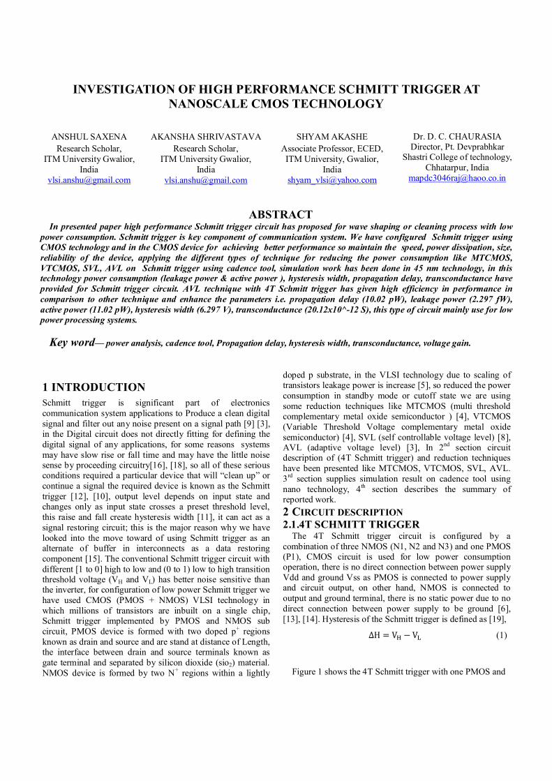
The 4T Schmitt trigger circuit is configured by a combination of three NMOS (N1, N2 and N3) and one PMOS (P1), CMOS circuit is used for low power consumption operation, there is no direct connection between power supply Vdd and ground Vss as PMOS is connected to power supply and circuit output, on other hand, NMOS is connected to output and ground terminal, there is no static power due to no direct connection between power supply to be ground [6], [13], [14]. Hysteresis of the Schmitt trigger is defined as [19],
∆H = V − V (1)
Figure 1 shows the 4T Schmitt trigger with one PMOS and
INVESTIGATION OF HIGH PERFORMANCE SCHMITT TRIGGER AT NANOSCALE CMOS TECHNOLOGY
2
Fig. 1.shows the 4T Schmitt trigger
3NMOS circuit to be condensed mainly delay of the circuit where Vdd=0.7 V power supply and Vin is varied 0.7 V to 1.8 V.
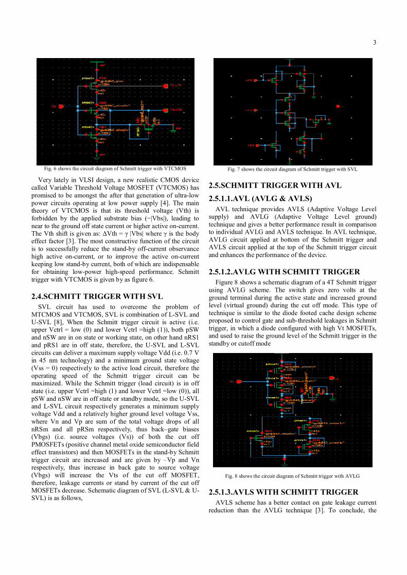
Fig. 2 Hysteresis width waveform of 4T Schmitt trigger
Figure 2 shows the Input-output waveform of the Schmitt trigger. It is also known as the hysteresis plot.
Fig. 3 Input-output waveform of 4T Schmitt trigger
Figure 3 shows the input–output waveform of Schmitt trigger in nanoscale technology using cadence tool, when input voltage Vin = 0.7 V and Vth = 0.7 V.
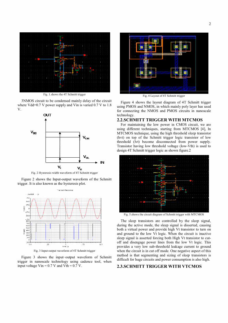
Fig. 4 Layout of 4T Schmitt trigger
Figure 4 shows the layout diagram of 4T Schmitt trigger using PMOS and NMOS, in which mainly poly layer has used for connecting the NMOS and PMOS circuits in nanoscale technology. 2.2.SCHMITT TRIGGER WITH MTCMOS
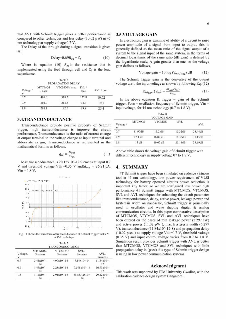
For maintaining the low power in CMOS circuit, we are using different techniques, starting from MTCMOS [4], In MTCMOS technique, using the high threshold sleep transistor (hvt) on top of the Schmitt trigger logic transistor of low threshold (lvt) become disconnected from power supply. Transistor having low threshold voltage (low-Vth) is used to design 4T Schmitt trigger logic as shown figure.2
Fig. 5.shows the circuit diagram of Schmitt trigger with MTCMOS
The sleep transistors are controlled by the sleep signal, during the active mode, the sleep signal is disserted, causing both a virtual power and provide high Vt transistor to turn on and ground to the low Vt logic. When the circuit is inactive sleep signal is asserted forcing both High Vt transistor to cut-off and disengage power lines from the low Vt logic. This provides a very low sub-threshold leakage current to ground when the circuit is in cut off mode. One negative aspect of this method is that segmenting and sizing of sleep transistors is difficult for huge circuits and power consumption is also high.
2.3.SCHMITT TRIGGER WITH VTCMOS
3
Fig. 6 shows the circuit diagram of Schmitt trigger with VTCMOS
Very lately in VLSI design, a new realistic CMOS device called Variable Threshold Voltage MOSFET (VTCMOS) has promised to be amongst the after that generation of ultra-low power circuits operating at low power supply [4]. The main theory of VTCMOS is that its threshold voltage (Vth) is forbidden by the applied substrate bias (−|Vbs|), leading to near to the ground off state current or higher active on-current. The Vth shift is given as: ΔVth = γ |Vbs| where γ is the body effect factor [3]. The most constructive function of the circuit is to successfully reduce the stand-by off-current observance high active on-current, or to improve the active on-current keeping low stand-by current, both of which are indispensable for obtaining low-power high-speed performance. Schmitt trigger with VTCMOS is given by as figure 6.
2.4.SCHMITT TRIGGER WITH SVL SVL circuit has used to overcome the problem of
MTCMOS and VTCMOS, SVL is combination of L-SVL and U-SVL [8], When the Schmitt trigger circuit is active (i.e. upper Vctrl = low (0) and lower Vctrl =high (1)), both pSW and nSW are in on state or working state, on other hand nRS1 and pRS1 are in off state, therefore, the U-SVL and L-SVL circuits can deliver a maximum supply voltage Vdd (i.e. 0.7 V in 45 nm technology) and a minimum ground state voltage (Vss = 0) respectively to the active load circuit, therefore the operating speed of the Schmitt trigger circuit can be maximized. While the Schmitt trigger (load circuit) is in off state (i.e. upper Vctrl =high (1) and lower Vctrl =low (0)), all pSW and nSW are in off state or standby mode, so the U-SVL and L-SVL circuit respectively generates a minimum supply voltage Vdd and a relatively higher ground level voltage Vss, where Vn and Vp are sum of the total voltage drops of all nRSm and all pRSm respectively, thus back–gate biases (Vbgs) (i.e. source voltages (Vs)) of both the cut off PMOSFETs (positive channel metal oxide semiconductor field effect transistors) and then MOSFETs in the stand-by Schmitt trigger circuit are increased and are given by –Vp and Vn respectively, thus increase in back gate to source voltage (Vbgs) will increase the Vts of the cut off MOSFET, therefore, leakage currents or stand by current of the cut off MOSFETs decrease. Schematic diagram of SVL (L-SVL & U-SVL) is as follows,
Fig. 7 shows the circuit diagram of Schmitt trigger with SVL
2.5.SCHMITT TRIGGER WITH AVL 2.5.1.1.AVL (AVLG & AVLS)
AVL technique provides AVLS (Adaptive Voltage Level supply) and AVLG (Adaptive Voltage Level ground) technique and gives a better performance result in comparison to individual AVLG and AVLS technique. In AVL technique, AVLG circuit applied at bottom of the Schmitt trigger and AVLS circuit applied at the top of the Schmitt trigger circuit and enhances the performance of the device.
2.5.1.2.AVLG WITH SCHMITT TRIGGER Figure 8 shows a schematic diagram of a 4T Schmitt trigger
using AVLG scheme. The switch gives zero volts at the ground terminal during the active state and increased ground level (virtual ground) during the cut off mode. This type of technique is similar to the diode footed cache design scheme proposed to control gate and sub-threshold leakages in Schmitt trigger, in which a diode configured with high Vt MOSFETs, and used to raise the ground level of the Schmitt trigger in the standby or cutoff mode
Fig. 8 shows the circuit diagram of Schmitt trigger with AVLG
2.5.1.3.AVLS WITH SCHMITT TRIGGER AVLS scheme has a better contact on gate leakage current
reduction than the AVLG technique [3]. To conclude, the

4
AVLS approaches, while more victorious in reducing the gate leakage current, still leaves two gate leakage current components in access transistors unaltered. It too leaves one sub-threshold current component in access transistor unchanged and results in an additional sub-threshold leakage current across the other access transistor, AVLS technique with 4T Schmitt trigger is as follows,
Fig. 9 shows the circuit diagram of Schmitt trigger with AVLS
Fig. 10 shows the circuit diagram of Schmitt trigger with AVL
Above figure shows the 4T Schmitt trigger with the AVL (AVLG & AVLS) techniques at different input voltage (Vin = 0.7 to 1.8 V) at Vdd= 0.7 V
3. SIMULATION RESULT Schmitt trigger Simulation has been done on cadence tool
using the 45nm technology with a nominal supply voltage Vdd = 0.7 V. The gate leakage being the only dominant mechanism at room temperature 27°C, different techniques have used for reduction of power consumption and maintaining the performance of Schmitt trigger, AVL method suppresses the maximum total leakage in comparison to MTCMOS, VTCMOS and SVL techniques, it improve the parameter like transconductance, propagation delay, leakage power, active power, and hysteresis width.
3.1.POWER ANALYSIS Power consumption is important parameter for VLSI
technology, there are two type of power dissipation one is active power and second is leakage power, and which are described as follows 3.1.1. ACTIVE POWER This power consumption during when Schmitt trigger is on state or working state. Essentially active power is estimated by giving input voltage and examines the average power consumption. The stop time for calculate active power is 200 ns. The active power is amalgamation of dynamic and static power consumption. Table 1 shows the active power of Schmitt trigger with MTCMOS, VTCMOS, SVL and AVL techniques and provided effective reduction in active power with AVL (11.02 pW) at input voltage 0.7 V.
Table 1 ACTIVE POWER
Voltage / V
AVL / pW
MTCMOS / nW
VTCMOS / nW
SVL / nW
0.7 80.62 60.41 35.04 11.02
0.9 100.5 108.8 90.4 21.1
1.8 134.6 120.4 101.6 47.4
Table 1 shows the active power analysis of Schmitt trigger with different techniques
Fig. 11 shows the graph of Active power
3.1.2. LEAKAGE POWER When we reduce the channel length or provide scaling so
the leakage power is increase, Leakage power provides standby power of any device. Leakage current can arise from substrate injection effects and sub-threshold voltage. Leakage power is wastage of power supply and leakage power of Schmitt trigger is given by as
푃 = 퐼 .푉 (2)
Where Pleak is leakage power of Schmitt trigger, Ileak abbreviate for leakage current, Vdd is power supply
Leakage power of 4T Schmitt trigger =1.6 µW (3)
Leakage power of 4T Schmitt trigger with MTCMOS =22.62 pW (4)
020406080
100120140160
0.7 V 0.9 V 1.8 V
MTCMOS / nW
VTCMOS / nW
SVL / nW
AVL / pW

5
Leakage power of 4T Schmitt trigger with VTCMOS=14.91 pW (5)
Leakage power of 4T Schmitt trigger with SVL = 9.86 pW (6)
Leakage power of 4T Schmitt trigger with AVL = 2.297 fW (7)
Fig. 12 shows the circuit diagram of Schmitt trigger with SVL
Shows the waveform of leakage current of Schmitt trigger which provide help to find out the leakage power of circuit where leakage current is 1.76 pA and Vdd= 0.5 V, so Pleak = 0.88 pW
Table 2
LEAKAGE POWER Voltage / V
AVL / fW
MTCMOS / pW
VTCMOS / pW
SVL / pW
0.7 22.62 14.91 9.86 2.297
0.9 31.5 21.39 15.02 4.15
1.8 35.6 24.96 18.89 5.34
Fig. 13 shows the circuit diagram of Schmitt trigger with SVL
3.1.3. TEMPERATURE DEPENDENT POWER VARIATION
Temperature dependence of the sub threshold leakage current is most important in digital very large scale integration (VLSI) circuits generally operate at elevated temperatures due to the power consumption (heat generation) of the circuit. The
temperature rises from (-1oC) to (7oC) in a 45 nanoscale technology. In this technology, the major factor Of Ioff is the sub threshold leakage; therefore, the temperature dependence of Ioff provide the temperature dependence of the sub threshold leakage, Minimum active power and leakage power is (1.04 pW & 1.14 fW) respectively in Schmitt trigger with AVLG technique.
Table 3 ACTIVE POWER AT DIFFERENT TEMPERATURES
temperature/ ºC
AVL
MTCMOS VTCMOS SVL
-1 2.02µW 1.10nW 11.93pW 1.04pW
30 4.45µW 2.45nW 14.10pW 1.1.48pW
70 15.86µW 4.07nW 22.50pW 4.52pW
Table 4 LEAKAGE POWER AT DIFFERENT TEMPERATURES
temperature/ ºC
AVL
MTCMOS VTCMOS SVL
-1 12.2nW 2.10nW 1.93pW 1.14fW
30 16.45nW 4.15nW 3.10pW 2.28fW
70 20.86nW 5.07nW 2.50pW 4.12fW
3.2.HYSTERESIS WIDTH Schmitt trigger provide raise and fall in signal and which
provide the hysteresis width, Hysteresis is the property of superiority of the Schmitt trigger, in which the input threshold changes depending on whether the input is rising or falling [17], [1], [2],. Hysteresis width is given by ∆H,
∆H = V − V (8)
V = 8.39V, V = 2.10V, ∆H = 6.29V (9)
Table 5 HYSTERESIS WIDTH
Voltage / V
AVL / V
MTCMOS / mV
VTCMOS / V SVL / V
0.7 5.23 2.54 5.16 6.29
0.9 2.16 1.65 1.31 3.15
1.8 1.05 0.58 1.02 2.34
Above equation shows the hysteresis width of Schmitt trigger 6.29 V at input voltage (0.7 V) using AVL technique.
3.3.PROPAGATION DELAY Schmitt trigger is used in place of buffer and reduce delay
as well as power consumption. The most positive characteristic of Schmitt trigger is its adjustable threshold voltage, and it can be controlled, the threshold voltage can be chosen to be above or below 푉 /2, a voltage at which buffer usually operates [15]. Therefore a Schmitt trigger can be designed to switch faster than a buffer leading to a reduction in delay, the adjustable low-voltage threshold of the Schmitt trigger operates more noise and voltage glitches as compared to buffer. The time in use for a Schmitt trigger logic gate output to change after one or more inputs have changed is known as propagation delay. The simulation Results examine
0
20
40
60
80
100
0.7 V 0.9 V 1.8 V
AVL / fW
SVL / pW
VTCMOS / pW
MTCMOS / pW
6
that AVL with Schmitt trigger gives a better performance as compared to other techniques and less delay (10.02 pW) in 45 nm technology at supply voltage 0.7 V.
The Delay of the through during a signal transition is given as;
Delay=0.69푅 ∗ 퐶 (10)
Where in equation (10) 푅 is the resistance that is implemented using the feed through cell and C is the load capacitance.
Table 6
PROPAGATION DELAY Voltage / V
AVL / psec
MTCMOS / nsec
VTCMOS / nsec SVL / nsec
0.7 409.0 318.5 122.8 10.02
0.9 301.0 214.5 94.6 19.1
1.8 291.1 182.5 89.8 25.4
3.4.TRANCONDUCTANCE Transconductance provide positive property of Schmitt
trigger, high transconductance is improve the circuit performance, Transconductance is the ratio of current change at output terminal to the voltage change at input terminal and abbreviate as gm, Transconductance is represented in the mathematical form is as follows;
푔 = ∆∆
(11)
Max transconductance is 20.12x10^-12 Siemens at input 0.7 V and threshold voltage Vth =0.35 V and∆퐼 = 36.21pA, Vin = 1.8 V.
Fig. 14 shows the waveform of transconductance of Schmitt trigger in 0.9 V
in SVL technique
Table 7 TRANCONDUCTANCE
Voltage / V
AVL /
Siemens
MTCMOS / Siemens
VTCMOS / Siemens
SVL / Siemens
0.7 3.45x10^-14
4.97x10^-14 7.14x10^-14 11.84x10^-12
0.9 1.43x10^-14
2.28x10^-14 7.598x10^-14 16.73x10^-12
1.8 1.16x10^-14
2.01x10^-14 89.83.42x10^-14
20.12x10^-12
3.5.VOLTAGE GAIN In electronics, gain is examine of ability of a circuit to raise
power amplitude of a signal from input to output, this is generally defined as the mean ratio of the signal output of a system to the signal input of the same system, in the terms of decimal logarithmic of the same ratio (dB gain) is defined by the logarithmic scale, A gain greater than one, so the voltage gain defines as follows,
Voltage gain = 10 log (V / )dB (12)
The Schmitt trigger gain is the derivative of the output voltage w.r.t. the input voltage as shown by following Eq. (12)
K (V ) = ( ) (13)
In the above equation K trigger = gain of the Schmitt trigger, Fosc = oscillation frequency of Schmitt trigger, Vin = input voltage, for 45 nm technology (0.7 to 1.8 V).
Table 8
VOLTAGE GAIN Voltage / V
AVL
MTCMOS VTCMOS SVL
0.7 11.97dB 13.2 dB 15.32dB 28.44dB
0.9 12.1 dB 16.89 dB 18.32dB 31.15dB
1.8 13 dB 19.67 dB 20.14dB 33.69dB
Above table shows the voltage gain of Schmitt trigger with different technology in supply voltage 07 to 1.8 V.
4. SUMMARY 4T Schmitt trigger have been simulated on cadence virtuoso
tool in 45 nm technology, low power requirement of VLSI technology for battery operated circuits power reduction is important key factor, so we are configured low power high performance 4T Schmitt trigger with MTCMOS, VTCMOS, SVL and AVL techniques for enhancing the circuit parameter like transconductance, delay, active power, leakage power and hysteresis width on nanoscale, Schmitt trigger is principally used in oscillator and wave shaping digital & analog communication circuits, In this paper comparative description of MTCMOS, VTCMOS, SVL and AVL techniques have been offered on the bases of min leakage power (2.297 fW) and active power (11.02 pW ), max hysteresis width (6.297 V), transconductance (11.84x10^-12 S) and propagation delay (10.02 psec ) at supply voltage Vdd=0.7 V, threshold voltage (0.35 V) and input control voltage varies from 0.7 to 1.8 V. Simulation result provides Schmitt trigger with AVL is better than MTCMOS, VTCMOS and SVL techniques with little propagation delay in (psec).this type of Schmitt trigger design is using in low power communication systems.
Acknowledgment This work was supported by ITM University Gwalior, with the calibration cadence design system Bangalore.
7
REFERENCE Yuan F., “A high-speed differential CMOS Schmitt trigger with regenerative current feedback and adjustable hysteresis," Analog Integrated Circuit and Signal Processing, Vol.63, No.1, pp.121-127, 2010.
Yuan F., “Differntial CMOS Schmitt trigger with tunable hysteresis," Analog Integrated Circuit and Signal Processing, Vol.62, No.2, pp.245-248, 2010.
Mangalam H., et.al, “Gate and subthreshold leakage reduction SRAM cells”, DSP Journal 6, Issue1, September, 2006.
Morimura H., et.al, “A zero sink current schmitt trigger and window flexible counting circuit for fingerprint sensors/identifier” IEEE International Solid State Circuit Conference (ISSCC), Vol.1, pp.122-517, 2004.
Kulkarni Jay deep P, et.al, “A 160mV robust schmitt trigger based sub-threshold SRAM," IEEE Journal of the solid-state circuit. Vol.42, No. 171-176, Oct 2007.
Kulkarni, Kim K, et.al, “A 160mV robust schmitt trigger based sub-threshold SRAM," IEEE J. Solid State Circuits, Vol.42, NO. 10, pp. 2303-2313, October 2007.
Yadav Monika, et.al, ” Analysis of Leakage Reduction Technique on Different SRAM Cells” International Journal of Engineering Trends and Technology- Volume2Issue3- 2011.
Mishra Meenakshi et.al, “Effect of MT and VTCMOS, on transmission gate logic for low power 4:1 mux in 45nm technology”, Seventh International confrence on Bio-Insired computing theories and application (BIC-TA 2012), Advance in intelligent system and computing, volume 202, pp 139-150, 2013.
Pedroni, “LOW-Voltage high speed schmitt trigger and compact window comparator," IEEE Electronics Letter, Vol.41, no.22, 1213-1214, 2005.
Kho Pham C. “Cmos Schmitt Trigger Circuit with controllable hysteresis using logical threshold voltage control circuit” IEEE Vol.36, No.1821-1824, 2007.
Reddy R. et.al, “high performance CMOS Schmitt Trigger” Vol.2 Issue, July- Augest 2012, pp.23, 1-2324.
Chen S.L.,et. al, “A new schmitt trigger circuit in a 0.13µ 1/2.5v CMOS processes to receive 3. 3v input signals," IEEE Transaction on Circuits and System 2; Express Briefs, Vol.52, issue 7. pp. 361-365, 2005.
Kundra Swati, et. al, “Low power Scmitt Trigger “ISSN 2222-1727 Vol.3, No.2, 2012.
Saini S., et.al, “Schmitt trigger as an alternative to buffer insertion for delay and power reduction in VLSI interconnects," TENCON 2009-2009 IEEE Region 10 conferences, pp. 1-5, 2009.
Yoichi, Sasaki, et.al, “Circuit and latch capable of masking soft error with schmitt trigger," Journal of Electronic Testing Vol. 24, No. 1-3 2008.
Singhanath Pratchayaporn, et.al, “DTMOS Schmitt Trigger with fully adjustable hysteresis” IPCSIT Vol.7 (2011).
Srinivasulu Avireni, “A Novel current Conveyon based schmitt trigger and its application as a relaxation oscillator” Vol.39, No. 678-686. Issue6. 29 ARP 2010.
Zafer Takhirav,et. al, “Error mitigation in digital logic using a feedback equalization with schmitt trigger (FEST) circuit” IEEE, Vol.22, No. 321-327, 2011.
Katyal V.,et. al, “Adjustable Hysteresis CMOS Schmitt Trigger," IEEE ISCAS, pp.1938-1941,2008.