investigation of neuristor biasing using pinch resistors...
TRANSCRIPT

Investigation of neuristor biasing using pinch resistors
Item Type text; Thesis-Reproduction (electronic)
Authors Leone, Ronald Alphonse, 1946-
Publisher The University of Arizona.
Rights Copyright © is held by the author. Digital access to this materialis made possible by the University Libraries, University of Arizona.Further transmission, reproduction or presentation (such aspublic display or performance) of protected items is prohibitedexcept with permission of the author.
Download date 02/07/2018 10:25:49
Link to Item http://hdl.handle.net/10150/318188

INVESTIGATION OF NEURISTOR BIASING USING PINCH RESISTORS
byRonald Alphonse Leone
A Thesis Submitted to the Faculty of theDEPARTMENT OF ELECTRICAL ENGINEERING
In Partial Fulfillment of the Requirements For the Degree of
MASTER OF SCIENCE
In the Graduate CollegeTHE UNIVERSITY OF ARIZONA
1 9 6 9
STATEMENT BY AUTHOR
This thesis has been submitted in partial fulfillment of requirements for an advanced degree at The University of Arizona and is deposited in the University Library to be made available to borrowers under rules of the Library.
Brief quotations from this thesis are allowable without special permission, provided that accurate acknowledgment of source is made. Requests for permission for extended quotation from or reproduction of this manuscript in whole or in part may be granted by the head of the major department or the Dean of the Graduate College when in his judgment the proposed use of the material is in the interests of scholarship. In all other instances, however, permission must be obtained from the author.
• „ / /ASIGNED: fCCT/’-Ji A sjjLCMJL.
APPROVAL BY THESIS DIRECTOR
This thesis has been approved on the date shown below:
R. L. Call DateAssociate Professor of Electrical Engineering

ACmoWI^DGMENTS
The author wishes to thank Dr» R. Call for his thoughtful helpand guidance in writing this thesis; also Dr. R. H. Mattson for hisencouragement and assistance; and Mr. E. D. Smith for his intelligent direction.
The author also wishes to express his appreciation to the staffof the Solid State Engineering Laboratory especially R. J. Baida,N. Hodge, Wo J. Lillis, L. Raymond, and V. A. Wells for their coopera
tion in the fabrication processes.Finally, the author gratefully acknowledges Mrs. Freida H. Long
for her invaluable help in typing the manuscript®

TABLE OF CONTENTSPage
LIST OF ILLUSTRATIONS . . ............ vLIST OR TABLES v HABSTRACT . . . . . . . . . . . . . . . .......... . . . . . . . . . viiiCHAPTER
1 INTRODUCTION . . . . . . . . . . . . . . . 1The Pinch Resistor . . . . . . . ................... 9Fabrication . . . 12
2 "DOG-BONE" PINCH RESISTOR . . . . . . . . . . . . . 1 . . 13Assumptions . . . . . . . . . . . . . . 13Channel Conductance . . . . . . . . . . . . . . . . . 16Process Evaluation . . . . . . . . . . . . . . . . . 20Experimental Results . . . . . . . . 22Breakdown Voltage Considerations . . . . . . . . . . I 25
3 CIRCULAR PINCH RESISTOR . . . . . . . . . . . . . . . . . 31
Processing Schedule . . . . . . . . . . . . . . . . . 32Device Characteristics . . . . . . . . . . . . . . . 36Device Evaluation . . . . . . . . . . . 52
4 CONCLUSION . . . . . . . . . . . . . . . . . . 61APPENDIX A: DERIVATION OF THE CHANNEL CONDUCTANCE OF A "DOG-
BONE" PINCH RESISTOR . . . . . . . . . . . . . . . . 62APPENDIX B: DERIVATION OF THE CHANNEL CONDUCTANCE OF A CIRCULAR
PINCH RESISTOR . . . . . . . . . . . . . . . . . . . 67LIST OF REFERENCES . . . . . . . . . . . . . . . . . . . . . . . 70

LIST OF ILLUSTRATIONSFigure Page
1.1 A Unijunction Transistor . . . . . . . . . . . . . . . . 21.2 First Order UJT Equivalent Circuit . . . . . . . . . . . 31.3 UJT Characteristic Curve . . . . . . . . . . . . . . . . 51.4 Typical UJT Biasing Configuration . . . . . . . . . . . . 61.5 UJT Characteristic Curve and Load Line . . . . . . . . . 71.6 Change in Second UJT’s Curve Due to Firing
of First UJT . . . . . . . . . . . . . . . . . . . . . . 81.7 A Top and Gross Sectional View of a "Dog-bone” Pinch
Resistor . . . . . . . . . . . . . . . . . . . . . . . . 112.1 A "Dog-bone" Pinch Resistor Structure Showing the
Coordinate System Used in the Diffusion Equations . . . . 14.2.2 Typical FET Curves Showing Region of Operation . . . . . 182.3 Boron Impurity Distributions for Two Drive**in Times . . . 30
3.1 Cross Sections View of a Circular Pinch Resistor . . . . 333.2 The Metallization Pattern of a Circular Pinch Resistor . 343.3 Circuit Used to Obtain Circular Pinch Resistor
Characteristics . . . . . . . . . . . . . . . . . . . . . 373.4 The I-V Characteristic of a Circular Pinch Resistor with
Both Gates at 8.9V . . . . . . . . . . . . . . . . . . . 383.5 Cross Sectional View of a Circular Pinch Resistor with
Both Gates at 8.9V . . . . . . . . . . . . . . . . . . . 393.6 The I-V Characteristic of a Circular Pinch Resistor with
Both Gates Open . . . . . . . . . . . . . . . . . . . . . 41
3.7 Cross Sectional View of a Circular Pinch Resistor withBoth Gates Open . . . . . . . . . . . . . . . . . . . . . 42
v

vi
List of Illustrations (Continued)Figure Page
3.8 The I-V Characteristic of a Circular Pinch Resistor withthe Top Gate Connected to the Sweep and the Bottom GateOpen . . . . . . . . . . . . . . . . . . . . . . . . . . 44
3.9 The I-V Characteristic of a Circular Pinch Resistor withthe Top Gate Connected to the Sweep and the Bottom Gateat 8.8V . . . . . . . . . . . . . . . . . . . . . . . . . 45
3.10 Cross Sectional View of a Circular Pinch Resistor with the Top Gate Connected to the Sweep and the Bottom Gateat 8.8V . . . . . . . . . . . . . . . . . . . . . . . . . 47
3.11 The I-V Characteristic of a Circular Pinch Resistor withthe Top Gate Connected to the Sweep and the Bottom Gate
. at 15V . . . . . . . . . . . . . . . . . . . . . . . . . 49
3.12 The I-V Characteristic of a Circular Pinch Resistor withthe Top Gate at 8.9V and. the Bottom Gate Open . . . . . . 50
3.13 Cross Sectional View of a Circular Pinch Resistor withthe Top Gate at 8.9V and the Bottom Gate Open . . . . . . 51
3.14 The I-V Characteristic of a Circular Pinch Resistor withBoth Gates Grounded and the Outer Radius Swept with aNegative Voltage (All Voltages Relative to the InnerRadius) . . . . . . . . . . . . . . . . . . . . . . . . . 53
3.15 Pinch Resistor Circuit Symbol and First Order Model . . . 54
3.16 Test Circuit Used to Measure Parasitic Capacitance . . . 553.17 UJT Oscillator Test Circuit . . . . . . . . . . . . . . . 583.18 Neuristor Test Circuit . . . . . . . . . . . . . . . . . 59A. 1 Cross Sectional View of a "Dog-bone" Pinch Resistor
Showing the Coordinate System Used to Evaluate the Channel Conductance . . . . . . . . . . . . . . . . . . . 63
B.l Cross Sectional View of a Circular Pinch Resistor Including Terminal Voltages . . . . . . . . . . . 68

Table2.13.1
LIST OF TABLES
•'Dog-bone” Pinch Resistor Statistical Results . . . .Parasitic Capacitance as a Function of Gate Bias 'V o 11 age .. .. . . . . . . . . . . . . . . . . . . .
vii
Page23
57

ABSTRACT
The purpose of this work is to fabricate a biasing network for the realization of a fully integrated neuristor line. The design guidelines consist of the constraints imposed by the neuristor on resistor and capacitor values, tolerable breakdown voltages, and allowable space.
Pinch resistors are used to comprise the biasing circuit. The feasibility of using the parasitic capacitance associated with these resistors rather than additional capacitors is investigated.
The devices are ultimately tested in a neuristor circuit to evaluate their performance.
viii
Chapter 1 INTRODUCTION
The power loss associated with the transmission of electrical signals through ordinary passive paths such as finite diameter wire, can be significant in integrated circuits systems. To alleviate this problem, an active transmission path with no attentuation properties was studied by Crane, 1960. The device he postulated was termed a
neuristor since its operation was analogous to nerve axons. In this respect a signal is transmitted by triggering a monostable element
which in turn will trigger another such element until transmission is 'complete. In 1964, R. H. Mattson investigated the use of unijunction transistors as neuristor elements. His work has been continued and it
is in support of this study that this thesis is written.A unijunction transistor, UJT, is a three terminal device
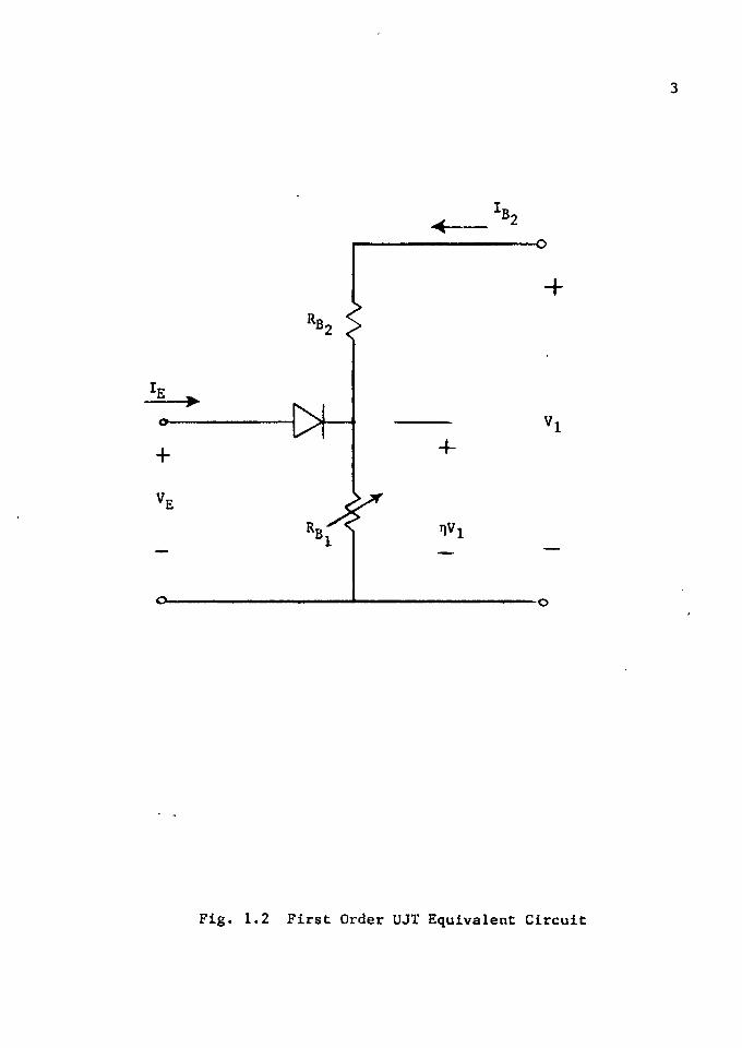
which is operated by triggering a reverse biased p-n junction. It
is shown symbolically in Fig. 1.1, and a first order equivalent circuit is given in Fig. 1.2. The bulk interbase resistance is expressed by Rg^ and Rgg. With the emitter open circuited and a voltage impressed across the base, , a voltage, , is set updirectly under the emitter as a result of the base resistance voltage divider effect. By triggering the emitter above , the junction will be forward biased and holes will be injected into the base

/
2
I B2<
Base-TwoEmitter
Base-One
Fig. 1.1 A Unijunction Transistor
3
Fig. 1.2 First Order UJT Equivalent Circuit
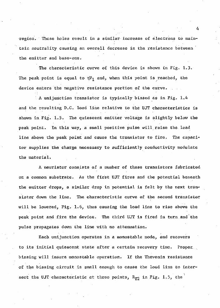
region. These holes result in a similar increase of electrons to maintain neutrality causing an overall decrease in the resistance between the emitter and base-one.
The characteristic curve of this device is shown in Fig. 1.3.The peak point is equal to and, when this point is reached, the
device enters the negative resistance portion of the curve.A unijunction transistor is typically biased as in Fig. 1,4
and the resulting D.C, load line relative to the UJT characteristics is shown in Fig. 1.5. The quiescent emitter voltage is slightly below the peak point. In this way, a small positive pulse will raise the load line above the peak point and cause the transistor to fire. The capacitor supplies the charge necessary to sufficiently conductivity modulate the material.
A neuristor consists of a number of these transistors fabricated on a common substrate. As the first UJT fires and the potential beneath the emitter drops, a similar drop in potential is felt by the next transistor down the line. The characteristic curve of the second transistor will be lowered. Fig. 1.6, thus causing the load line to rise above the
peak point and fire the device. The third UJT is fired in turn and the pulse propagates down the line with no attenuation.
Each unijunction operates in a monostable mode, and recovers
to its initial quiescent state after a certain recovery time. Proper, biasing will insure monostable operation. If the Thevenin resistance
of the biasing circuit is small enough to cause the load line to inter
sect the UJT characteristic at three points, In Fig. 1.5, the'
peak point
negative resistance region
valley point
Fig. 1.3 UJT Characteristic Curve
6
r2
Fig. 1.4 Typical UJT Biasing Configuration
7
Fig. 1.5 UJT Characteristic Curve and Load Line

8
E2
Before First UJT Fires
After First UJT Fires
E2
Fig. 1.6 Change in Second UJT’s Curve Due to Firing of First UJT

transistor will lock in a "low state" after firing and not recover to its previous quiescent state. To avoid this situation, the slope of the load line must be higher than the negative resistance region of the curve.
Although the negative resistance varies with the type of device, a safe load line slope is 5 Kfl. This specifies and Rg at 10 Kfi and
up.The capacitor is also dependent on the particular device. The
amount of charge necessary to decrease the emitter to base-one resistanceis determined by the amount of material in this region and the coupling
. -
between one UJT and the next. Another factor is the position of the static operating point. If the device can be biased directly beneath the peak point, a minimum capacitance is required. A reasonable value for the neuristors processed in the Solid State Engineering Laboratory at The University of Arizona-is between SO and 200 pf.
The Pinch ResistorIn integrated circuits, resistors are easily made during the
same diffusion as the base region of a bipolar transistor. Values arelimited by the space available on a chip. The space required for a
210 Kfl resistor is In the neighborhood of 50 mil . The shortcomings of diffused resistors for neuristor biasing are obvious. A neuristor line may consist of three or more unijunction transistors, or a minimum of six resistors.
An alternate method is the use of pinch resistors. They can be made to have an effective resistance of twenty times a similar diffused

/
10resistor» Such a device is essentially a junction field effect transis
tor which is operated below pinch off» It is constructed by diffusing
a channel into an substrate, which forms the bottom gate. A top
gate is formed by an ?W ? diffusion into the channel. A pinch resistor, using a fldog~bones? geometry is shown in Pig. 1.7. .
The channel is L long, Z wide and 2a thick. The 8sp" channel is
fabricated in the same manner as the base of a bipolar transistor. It
is different from a diffused resistor in two respects. First, the con
ducting portion of the resistor, the channel, is well below the surface of the wafer where its conductivity is much lower than at the surface. .
Second,, the depletion in the channel due to the reverse biased p-n junc^
tions, i.e., channel to gate junction, will reduce the amount of area available for current flow, hence, increasing the resistance of the chan
nel even more.
In neuristor applications the resistor is operated in the following manner. The two gates are biased positively with respect to the most positive region of the channel. This insures that both junc
tions are everywhere reverse biased. A voltage is then put across the
resistor. As current flows down the'channel, the potential corresponds
ingly drops along the length of the channel. This leads to a larger voltage .across the junctions and a larger depletion region. This chan
nel depletion also lends versatility to the device since the resistance
can be varied by changing the gate bias.
The pinch resistor solves very nicely the problem of obtaining
a large resistor using very little space. Another problem, however, is
11
L * Channel Length Z » Channel Width K — 3Z — M
1zT
/\ \
zZ / / , K
(a) Top View
z
wafersurface Channel-top Gate Junction
Source Drainn+n Top Gate
p" channel 2a
" Channel-Bottom Gate Junctionn" Bottom Gate
(substrate)
(b) Cross sectional View
Fig. 1.7 A Top and Cross Sectional View of a "Dog-bone" Pinch Resistor

12
that of making a capacitor which will foe large enough to trigger each unijunction transistor* Associated with every p-n junction is a para
sitic capacitance due to the depletion layer * By making use of this
fact, the need for designing a separate capacitor can be eliminated*The capacitance of a p-n junction is dependent on the width of
the depletion layer, hence impurity concentration and applied voltage.
It is also proportional to the junction area* In this respect a diffused resistor with its large area would be more efficient than a pinch
resistor * Different pinch resistor geometries are tried to circumvent
this problem and a compromise between minimum capacitance and minimum
space is obtained*
Fabrication
The resistors are fabricated on a different chip than the neuris-
tors* This is done to allow the utmost in processing flexibility and to avoid any unwanted biasing noise in the neuristor line* The resistors are fabricated on 0*1 ohm-cm material opposed to 100 ohm-cm material
used for the neuristors* This facilitates processing due to the extensive data available in the Solid State Engineering Laboratory on this
material*
Ultimate neuristor realization consists of mounting two separate
chips, neuristor and resistors, on a common header, using a common supply voltage*

Chapter 2
"DOG BONE" FINCH RESISTOR
The first set of pinch resistors were made compatible with the
bipolar transistors fabricated in the Solid State Engineering Laboratory
of The University of. Arizona0 The transistors have base and emitter
junctions of approximately 3p and 2p respectively from.the surface of
the wafer, and the emitter-base breakdown voltage is typically 8 volts. The processing of the resistors was identical to these transistors,
therefore, all the parameters were fixed, and the only variable was the
length of the resistor.
Assumptions
To simplify the calculations on a first order level, the equations which will follow were derived using the following assumptions.
1. The two "n" gates are much more heavily doped than the channel,
Fig. 2«,lo Therefore, most of the depletion region is in the
channel, thereby, directly relating change in channel current
to change in total depletion width. In fabricating the device
this is not true since the bottom gate is of lower concentration than the channel.
2. Shockleyfis "gradual approximation" is used (Shockley, 1952).
This states that the field, E, in the depletion region is in the
y direction only, and in the undepleted portion of the channel
in the x direction only. The voltage across the junctions can13

Gate
SourceT2a
1
:;*<W) - V « 0 H(«)Drain'b(W)+ V(x)
Gate6 V,
Fig. 2.1 A "Dog-bone" Pinch Resistor Structure Showing the Coordinate System Used in the Diffusion Equations

15then be found by using static conditions, and then applied to
the case when current flows. The gradual -approximation gives
more accurate results when the current is small, hence, a
smaller change in depletion width along the channel.
3. The leakage current across the reverse biased junctions is
neglected. The channel current is then a constant and not a
function of x.
4. The built-in contact potential across the junctions is con
sidered negligible compared to the operating voltages.
5. The impurity concentration of the channel is assumed to be con
stant. This is true in the x and z directions, but not in the
y direction. Pig. 2.1. The conductivity throughout the channel
is assumed the same as the conductivity, of the material at
the top junction.
6. The substrate is also assumed to have a constant doping profile.
This is true for epitaxially grown wafers. Non-epi wafers do not correspond as closely to this assumption.
7. It is assumed there is no emitter push. Emitter push refers
to a depression of the channel directly below the top gate due
to a strain on the lattice structure during phosphorous pre-
deposition. In neglecting emitter push the depth of the
channel-bottom gate junction is found directly from the
diffusion equation.
8. The resistance of the end pads is assum&d negligible compared to
the channel resistance and, therefore, is not included in the
calculations.

16Channel Conductance
The depletion width of a p-n junction with constant doping and
neglecting the contact potential is given by (Hamilton and Lindholm,
in press).
<2-i)
Where
tyPG channel impurity concentration
« Hni? type gate impurity concentration
W(x) 555 the voltage across the junction
• Y_ = depletion width in the Hp?5 material PYn 58 depletion width in the "nrf material
The first approximation states that Ng » therefore, the depletion
region is in the channel only and is
Yp(w) ” [ f 5 % ] [ ] (2-2)
The channel concentration is assumed constant, therefore, only half the
channel need be considered. The voltage necessary to pinch the channel
off corresponds to that voltage which will fully deplete the channel;
hence, for pinch off
Yp = a (2,3)
Where
a = one-half the channel thickness. Fig, 2,1
The pinch off voltage can be found by substituting Eq. (2,3) into Eq„
(2,2) and obtaining

17
“° = [ i r ] a2 (2-4)
WhereWQ = pinch off voltage
From previous diffusions the average sheet resistance, ps , of
the channel can be assumed to be 200 ohms/sq. This corresponds to an17 3impurity concentration, of 1.5 x 10 /cm at 2\x below the surface.
The channel thickness, 2a, is Ip. Knowing this, Eq. (2.4) yields a pinch off voltage of 28.9 volts.
This comparatively high pinch off voltage is very desirable.The voltage across the junction is never greater than the emitter-base breakdown voltage of eight volts, and in reference to junction field- effect transistors. Fig. 2.2 the region of operation is consequently on the linear portion of the curves. The resistance of the channel has
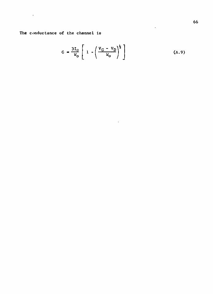
minimum sensitivity to operating voltages.As derived in Appendix A, the conductance, G, of the channel
below pinch off is
WhereIQ » pinch off current
v VG = the gate voltage relative to the source
Vn “ the drain voltage relative to the source

(raa)
Region of operation of pinch resistors is on linear region of the FET curve.
1.1-
0.7-
10 V0.4-
403020(volts)
Fig. 2.2 Typical FET Curves Showing Region of Operation00
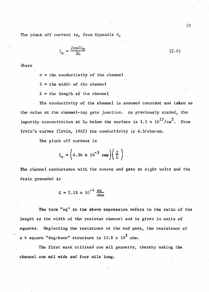
The pinch off current is, from Appendix A>
2<raZW0 Io " 3L
Wherecr = the conductivity of the channelZ = the width of the channelL = the length of the channel The conductivity of the channel is assumed constant and taken as
the value at the channel-top gate junction. As previously stated, the impurity concentration at 2p below the surface is 1.5 x 10^/cnf*, FromIrvin’s curves (Irvin, 1962) the conductivity is 4.5/ohm-cm.
The pinch off current is
The channel conductance with the source and gate at eight volts and the
drain grounded is
C » 2.13 x 10⁻⁴
The term ”sq’' in the above expression refers to the ratio of thelength to the width of the resistor channel and is given in units ofsquares. Neglecting the resistance of the end pads, the resistance of
3a 4 square "dog-bone” structure is 18.8 x 10 ohm.The first mask utilized one mil geometry, thereby making the
channel one mil wide and four mils long.
(*•34 x 10 amp)
19
(2.6)

20
Process EvaluationThe resistors were fabricated using the same processing sche
dule as the bipolar transistors made in the Solid State Engineering Laboratory. A comparison between the theoretical predictions and the experimental results is now given to obtain additional information for future processing of resistors.
mately 0.1 ohm-cm, polished at The University of Arizona. The "p" type channel was achieved by a boron predeposition and drive-in, while the "n" type top-gate consisted of a phosphorous predeposition and drive-in. The predeposition of phosphorous and boron is assumed two dimensional. This precludes diffusion into the bulk and allows the predeposition to be treated as a surface density. In this manner the diffusion equation
can be solved by assuming a delta function input.The effective surface density, Qtp, acquired during predeposi
tion is found by integrating the impurity concentration (Grove, 1967)
The wafers consisted of "n" type non epitaxial material approxi-
00
(2.7)
WhereNq = solid solubility of "n” type silicon Dp » predeposition diffusion constant tp =» predeposition time
Upon integration

21
Qtp = V F P Patomcm2 (2.8)
The impurity profile due to drive-in is given by (Warner, 1965)
e-y2/4Ddtd (2.9)
Wheretd = drive-in time
From previous results in the laboratory a base junction depth of 3p was obtained after a three hour drive-in, and a drive-in diffusion
can be solved for . The surface density due to a boron predeposition
the top gate drive-in to be negligible for the following reasons. The phosphorous drive-in temperature, 1100°C, is less than that for boron, 1160°C, hence, the boron diffusion coefficient at 1100°C will be less
than at 1160°C. The phosphorous drive-in time is small compared to that
for boron, approximately twenty minutes versus three hours. It is also assumed that there is no emitter push due to lattice strain during phosphorous predeposition.
From previous processing results, a 2n junction depth occurs after approximately a twenty minute phosphorous drive-in.
constant, Dd ■ 2.2 x 10 ji2/hr., was calculated. With this information17 3and assuming the substrate concentration is a uniform 10 /cm , Eq. (2.9)
;pis Qtp ■ 4.36 x 10 /cm2.
One can assume the amount of additional channel diffusion during

Experimental ResultsAs stated before*, the resistors underwent a boron drive®in cycle
of three hours. The necessary phosphorous drive®in time was not as certain since previous results in the laboratory indicated that a variation of five to ten minutes existed in obtaining the 2p. junction* For this reason^ one wafer was driven®in for 15 minutes^ while the other was driven®in for 20 minutes* In this way it was assured that a one micron channel would be obtained on one of the wafers and that two dif® ferent channel thicknesses would provide greater insight in evaluating
the data»Using an external gate bias the finished resistors were tested
on a curve tracer* Both wafers exhibited large variations in resistor
values, ranging from-2 to 16 KS2* There was very .little difference be* tween the two wafers since each had a wide spread of values and a.common breakdown voltage of approximately 8 volts* An immediate explanation for the large variation is the fact that the wafers used did not have epi® taxially grown substrates, therefore, the previous assumption that the
substrate concentration was constant is not valid* Other possible sources of non®uniformity are: uneven impurity gas flow in the diffusionfurnaces, uneven heating, and non-uniform polishing giving rise to dif
ferent surface conditions*Table 2*1 shows the distribution of resistance values over both
wafers * The 20 minute wafer, wafer B, was diced and mounted on headers
before all the devices were checked* Only a limited number of resistors were looked at, therefore, it is not as true a measure as the data for

23
Table 2.1"DOOBONE" PINCH RESISTOR STATISTICAL RESULTS
Wafer A Wafer BResistance in
Kilohms15 minute
Number of Devices
drive-in Percent of Total
20 minute drive-in Number of Percent
Devices of Total
2-3 13 4.4% 0 0.0%3-4 35 12.0 3 4.04-5 35 12.0 6 8.15-6 32 11.0 14 19.06-7 33 11.0 20 27.07-8 26 8.8 19 25.68-9 21 7.1 7 9.59-10 27 9.2 2 2.710-11 33 11.0 1 1.411-12 21 7.1 0 0.012 and up -19 6.5 _2 2.7
Total No. of Devices 295 74
_______ J}

24
the 15 minute one, wafer A* Each locality of the wafer contained a preferred value such that the distribution of values over the water was
not randomo Those devices toward the edge tended to have higher resistances than the inner oneSo This can be partly explained by wafer imperfections near the extremities<, The devices toward the center of the wafers had values consistently between five and ten kilohms* Wafer A produced very low values at one end where the photoresist had lifted.
Both wafers were lapped and stained to determine the junction depths. This was difficult since a monitor wafer was not included in the processing. It was extremely difficult to keep track of the resistors after dicing, and only an approximate correlation between resistance value and junction depth was obtained.
A device on wafer A measuring 9 K£2 had a channel width of l.OSp,,
the junction depths being 2.19m. and 3.22m<> Also measured for a 10 K$2
device were junction depths of 2.25m and 3.54mo The validity of the conductance equation can be substantiated by obtaining theoretical resistance values for the above junction depths. The previously assumed
channel sheet resistance of 200 ohms/sq. is supplanted by 135 ohms/sq., which was obtained for a similar diffusion.
Using junction depths of 2.19m and 3.22m, the conductivity of the channel at the top gate junction is 5/ohm-cm. The 1.03 channelwould be pinched off at 32.2 volts and- the channel resistance should be
33.9 x 10 ohm/sq. In theory, the four square resistor should have had a total resistance, of 15.6 KB. The fact that the device measured only 9 Kfi may be due to poor staining and therefore erroneous junction depths.

25
Another discrepancy may be in the channel sheet resistance, pg =135 ohms/sq0 This value was not measured on wafer A but instead onanother wafer which was processed at the same time„
The second set of junction depths, 2.25p and 3.54#, requiredthat the conductivity of the channel be 6/ohm-cm. The 1.29# channelwould be pinched off at 67.2 volts. This is higher than - the previousdevice because of the wider channel. The resistance should he 2.0 x
310 ohms/sq., making the total resistance 8 Kfi. The device measured 10 Kfi, making these values in closer agreement than the previous set.
A device on wafer B, approximately 7 Kfi also had junction depths
of 2.25p and 3.54p. This yields as before, a theoretical total resistance of 8 Kfi, which is in very close agreement to the experimental value.
The resultant data indicate that the conductance equation, despite the gross assumptions, yields comparatively accurate results.
The original expected value of 18.8 Kfi was not obtained due to
a failure in the processing to achieve specified junction depths. This can be remedied by a variation in fabrication parameters, although it
is beyond the scope of this work.
Breakdown Voltage Considerations
The first set of resistors were made for the purpose of explor
ing its feasibility and uncovering any problems which may later arise. The design was made compatible with bipolar transistors because of the extensive processing information available, and not designed around any
26
neurisfcor constraints. With preliminary information in hand the resistors were now ready to be applied to the neuristor line.
Neuristors are typically biased at ten volts, and for success
ful integration of all elements, the pinch resistors must have a minimum breakdown voltage equal to or greater than this value. At this time it was decided to investigate the various means of raising the existing breakdown voltage. To facilitate fabrication the same set of masks as before were used.
The mechanism of junction breakdown is as follows. In every
reversed biased p-n junction there exists a depletion region consisting of negative and positive ions and to a good approximation devoid of mobile carriers. This space charge is voltage dependent, increasing in width with increasing voltage. The space charge associated with the
ions sets up an electric field which will accelerate thermally generated electrons from the silicon atoms. If the field is high enough, the electrons will have sufficient kinetic energy to break the interatomic covalent bonds and produce more hole electron pairs. The process quickly generates enough holes and electrons to constitute a large reverse current. The critical field necessary for breakdown is characteristic of the material.
For a given reverse voltage, the depletion region will be wider for a low impurity concentration. Thus, in a diffused p-n junction, the depletion region will be the most narrow at the surface, increase along
the sidewalls with increasing depth, and be greatest along the bottom. Because the same reverse voltage exists across all sections of the
27junction, the more narrow depletion region will produce the larger field.
Thus, a junction will breakdown near the surface where the impurity concentration is highest. For a one-sided junction, that is, one in which the depletion is predominantly on one side of the junction, the determining factor for breakdown will be the background or lower impurity concentration. This is due to the fact that the background material will contain most of the depletion region. By varying the background concentration, the depletion width and the electric field can
also be varied.The pinch resistor breakdown voltages can be increased by driving
the channel in farther which will also reduce the surface concentration.A limit is placed upon this due to boron absorption in the protective silicon dioxide layer. If the drive-in time is too long, enough boron
may diffuse into the SiOg to invert the surface to "n”.The value of the electric field necessary for junction breakdown
is (Grove, 1967)
WhereCB = the background concentrationBV = the breakdown voltage
Assuming the surface concentration to be 3 x 10^^/cm?, and the breakdown voltage 7.0 volts, the critical field of the first set of
28
resistors is 2.55 x 10^ volt/cm. Using this value, the necessary back-18 3ground concentration for a breakdown of 12 v. is Cg = 1.75 x 10 /cm .
To achieve this surface concentration, a new drive-in time had
to be determined. The charge deposited during the boron predeposition as well as the drive-in diffusion coefficient is the same as for the previous set of resistors. Thus, Qt^ = 4.36 x 10^/cm^ and Dj = 2.2 x
10 *|/Vhr. Substituting these values into the diffusion equation yields a drive-in time of nine hours. The corresponding junction depth is 4.75p.
The actual drive-in time used was 10.0 hours to insure the
desired background concentration would be achieved. Thus, the predicted junction depth is approximately 5.Op. The value actually obtained in the laboratory was 6.8p, considerably more than expected. The top gate was driven-in for a total of 4.5 hours, after which the junctions were 4.2p and 7.4p.
The experimental channel distribution corresponded to a diffusiv--1 2 -12 ity, Dd = 5.0 X 10 p /hr., instead of 2.2 x 10 p /hr. as observed on
the first set of resistors. It can be inferred that there are process
ing variables present which are specifically unknown, at this time. The possibilities include temperature variations from one run to another and gas flow irregularities in the oven.
The results of this run were disappointing in that the observed breakdown voltage was only ten volts compared to the 19 v. predicted value using the given junction depths. The measured resistance values lay between 1.6 and 1.8 kilohms, and in this respect the small variation

29
was a welcomed sidelight*, These results 'were very close to the theoretical value of 1,87 K&» This leads one to suspect the impurity concentrations are close to the predicted value a few microns into the material, but not at the surface.
The small increase in breakdown voltage may be due to boron absorption into the silicon dioxide and is explained as follows. As the drive-in cycle proceeds, the boron diffuses injto the SiOg and tends to lower the concentration at the surface as shown in Fig, 2,3, As the cycle further proceeds, the silicon dioxide will absorb less boron because of a smaller concentration gradient. The initial hump in the
impurity distribution will level off with time, keeping the concentration at the surface practically constant. It is then possible for a three hour drive-in to have almost the same surface concentration as a ten hour one, . Thus, the breakdown voltages will differ by only a
few volts.This method of raising the breakdown voltage is not satisfac
tory and other parameters must be varied. One possibility is lowering the amount of boron during predeposition. This will lower the surface concentration without the long bothersome drive-in period. The phos
phorous predeposition charge-can also be lowered thereby eliminating the one-sided junction, and increasing the depletion region: in.the top gate. The total depletion region can then be widened without having the channel absorb all the increase.

N(y)
Smaller surface concentration due to out diffusing
XDotted lines indicate
theoretical distribution.Solid lines indicate distribution taking into account boron out diffusion into Si0 2 *
Predicted surface concentration for drive-in time t
X—
t2 > t1
drive-in time t>
Fig. 2.3 Boron Impurity Distributions for Two Drive-In Times

Chapter 3
CIRCULAR PINCH RESISTOR
The Hdog-bone8i geometry described in Chapter 2 was found to have sufficient resistance, but lacked enough parasitic capacitance to fire a unijunction transistor, hence, a neuristor line. To fully integrate the neuristor biasing network, the necessary capacitance must be achieved either by employing a separate diffused capacitor or by varying the geometry of the pinch resistor in such a way as to increase its parasitic capacitanceo To fully utilize chip space it was decided to in- verstigate the possibilities of the latter solution.
The capacitance of a p-n junction can be increased in two ways. The first consists in minimizing the depletion width by increasing the impurity concentrations on one or both sides of the junction. This can
be seen by examining the equation for junction capacitance (Hamilton,
Lindholm, in press).
c - ^ (3-i)
WhereA = the area of the p-n junction
As the impurity concentrations increase, the depletion width, + yn, decreases, hence, the capacitance increases- This technique is undesirable since a decreased depletion width will exhibit a lower breakdown voltage.
31
, 32Further examination of Eq. (3.1) shows that the capacitance can
be augmented by increasing the junction area. To obtain this increase in junction area, a circular pinch resistor is very suitable. It represents a compromise between a diffused resistor and a ’’dog-bone" pinch resistor. The effective resistance per unit area associated with
a circular geometry is greater than a diffused resistor yet smaller than a "dog-bone" device. This results in a compromise which affords relatively large junction area compared to a "dog-bone" resistor, and also a
relatively large sheet resistance compared to a diffused resistor.The masks for the circular pinch resistors were made with a
"fly's eye" camera. The maximum available space was 24 x 24 mils. In order to obtain the highest capacitance, the device was designed as large as possible within the above mentioned dimensions. Figure 3.1
shows the basic configuration. The metallisation pattern is displayed in Fig. 3»2. The top gate contact is independent of the bottom gate contact. This provides considerable flexibility in operating the device.
Processing ScheduleThe processing of these devices was similar to the bipolar
transistor fabrication discussed earlier with the following alterations. While constructing these devices for a suitable resistance and capacitance, it was hoped that a method might be found to also raise the break
down voltage. The technique of driving the channel and top gate farther into the substrate as described in Chapter 2 was met with limited
success. Since breakdown is presumed to take place at the surface where

33
p" channel
n" substrate (bottom gate)
Fig. 3.1 Cross Sectional View of a Circular Pinch Resistor

\ x - x -Bottom
\ Gate
Drain
Bottom
Fig. 3.2 The Metallization Pattern of a Circular Pinch Resistor

35
the impurity concentration is highest, a method for decreasing the surface concentration alone was employed.
As discussed in Chapter 2, boron is soluble in silicon dioxide.
This fact results in the absorption of the boron near the surface by the silicon dioxide grown during the channel drive-in cycle. As the silicon dioxide absorbs more boron, the concentration gradient between silicon and SiOg is lowered, resulting in a smaller boron absorption as time progresses. The boron absorption, or leaching, can be enhanced by aborting the drive-in cycle after a predetermined time, etching the
boron rich SiOg and growing a new layer while completing the drive-in. This can be done several times if necessary.
The fabrication commenced with a 15 minute boron predeposition into an epitaxially grown substrate with a resistivity of 0.18 ohm-cm. The oxygen content was raised from 6 to 10 percent to further lower the
boron concentration. The resulting sheet resistance was 46 ohms per square. The wafer was then driven-in for 30 minutes in a steam atmos6-
phere, after which the oxide layer was removed and the sheet resistance found to be 120 ohms per square, a significant increase. The drive-in
cycle was completed with an additional 60 minute steam and 90 minute dry nitrogen, for a total of three hours. The sheet resistance after
the three hour boron drive-in was 172 ohms per square, and the resulting junction depth was 3.86 microns.
A 15 minute phosphorous predeposition was then made. This was followed by a drive-in cycle consisting of a steam atmosphere for 25 minutes and a dry nitrogen atmosphere for 35 minutes. The two junction

36
depths were 3.08|J. and 4.05^ after the phosphorous drive-in cycle. The resultant channel thickness was 0.97(1.
Device CharacteristicsAfter the processing was completed, the devices were tested on
a curve tracer. Several interesting modes of operation were available due to the individual gate connections.
The resistor was first operated as shown in Fig. 3.3. Both gates were biased at approximately +8.9 V relative to ground and the inner radius of the channel was grounded. The outer radius of the
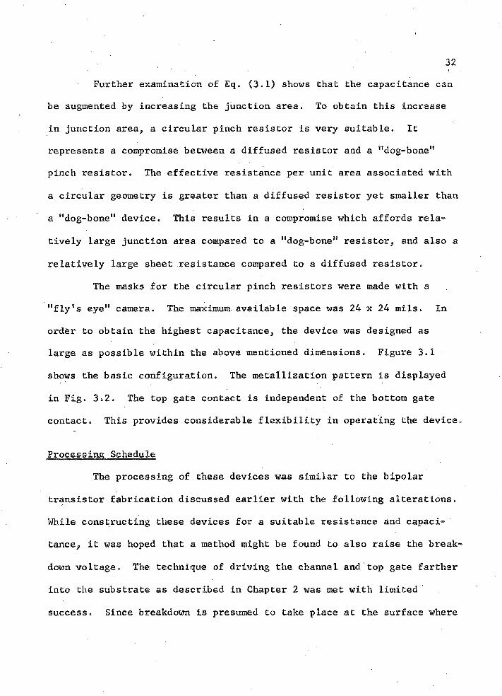
channel was connected to a sweep voltage. The resultant current-voltage relationship is displayed in Fig. 3.4. The shape of the curve can be explained physically in a simplified manner by focusing attention on the depleted and undepleted volume of the channel as depicted in Fig. 3.5.
The inner radius is and the voltage across the depletion region at this point is denoted as W(r^). When the sweep voltage, connected at the outer radius, rg, is at a small value, e, the voltage across the depletion region at this point, WC^), is
W(r2) = 8.9V - e
which is close to 8.9 V, hence a fairly large depletion region exists at
this point. The voltage across the depletion region at r^ is W(r%) =8.9 V. As the sweep voltage increases with time, the voltage across the depletion region at x = r2 decreases, thereby decreasing the depletion region until finally, just before the junction is forward biased, the sweep is at the gate voltage and the voltage across the junction is zero.

37
Bottom < Gate
Drain
BottomGate
Fig. 3.3 Circuit Used to Obtain Circular PinchResistor Characteristics

38
I 0.5 ma/div
Vn 1 volt/division
Fig. 3.4 The I-V Characteristic of a Circular PinchResistor with Both Gates at 8.9V
39
n" top gate
+ p" channelc
nM bottom gate8.9V
(a) Small voltage across the channel
x
n" top gate8.9V
W(r
+p1' channel8.9V
n" bottom gate 9V(b) Large voltage across the channel
Fig. 3.5 Cross Sectional View of a Circular PinchResistor with Both Gates at 8.9V

40The depletion region at x = rg has been decreased but since the voltage W(r^) has remained the same, i.e., 8.9 V, the depletion region at x = r^ has stayed the same. The net effect is a lowering of channel resistance
as the sweep voltage increases due to a corresponding increase in conducting volume in the channel.
The I-V trace in Fig. 3.4 clearly indicates a decreasing resis
tance as the sweep voltage increases. At 9.5 V the sweep voltage has overcome the necessary 0.6 V contact potential to forward bias the gate-
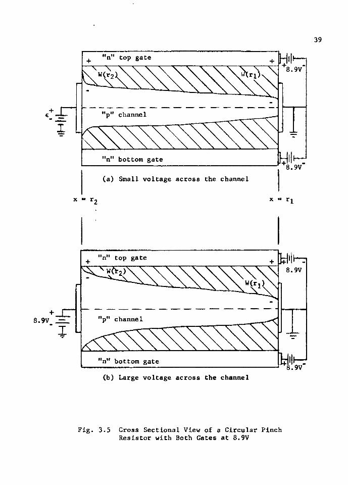
channel junction.The resistor was next tested by again sweeping the outer radius
and grounding the inner one, but now leaving both gates open. The result is presented in Fig. 3.6. One now finds the resistance increasing with sweep voltage. A possible explanation comes from again examining the depletion region. At low sweep voltage values, the depletion region is small and fairly constant along the length of the channel. This is due
to the lack of a reverse voltage across the junctions. As the sweep voltage increases, the p-n junctions will tend to be forward biased; however, no current flows across them because of the open gates. There will be no voltage drop across the junction near x = rg, i.e., where the junction is forward biased. The gates will then be at the same potential
as the sweep voltage. At the other end of the channel, x = r^, the p-n junction will be reversed biased. In other words, the gate will be at the positive sweep potential, yet the’inner radius is at ground potential,
hence a depletion region is formed near this end of the channel increas
ing with the sweep. This is shown in Fig. 3.7. It logically follows

41
-I 0.5 ma/dlv
W J -mmamummimmwMwmwtdmmmmmmmmVD 1 volt/division
Fig. 3.6 The I-V Characteristic of a Circular PinchResistor with Both Gates Open
'p" channel
’n” bottom gate >(a) Small voltage across the channel
n top gate
p" channel
n" bottom gate
(b) Large voltage across the channel
Fig. 3.7 Cross Sectional View of A Circular PinchResistor with Both Gates Open

43that as the sweep voltage increases, the depletion in the channel increases, thereby increasing the resistance. When the sweep voltage exceeds the breakdown voltage of the junction, the junction near the inner radius will break down.
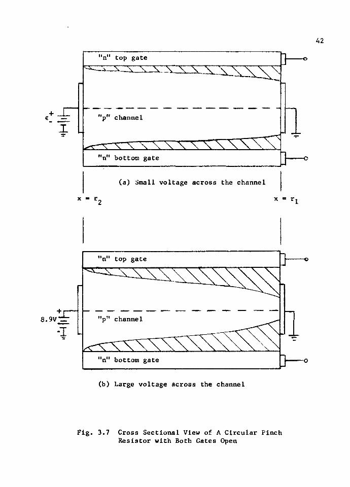
The bottom gate was then opened and the top gate connected to the sweep. The I-V characteristic is shown in Fig, 3.8. The result
is very similar to Fig. 3.6 in which both the gates were left open.The operation of the device is in fact the same in both cases.
The bottom gate will become forward biased near x = rg as the sweep voltage is increased. This clamps the bottom gate to the sweep, as was the case when both gates were open. The top gate now is connected to the sweep, but this also was true when it was open. The net result of opening the bottom gate and connecting the top one to the sweep is . the same as leaving both gates open. By comparing Fig. 3.6 with Fig.3.8, it can be seen that the resistance, point for point, along the trace is almost exactly the same.
The ensuing connection consisted of the bottom gate at a positive potential, approximately 8.8 V, and the top gate connected to the sweep voltage. The outer connection to the channel was again connected to the sweep voltage while the inner one was grounded. Figure 3.9 displays the subsequent I-V curve.
The curve is rather linear, the resistance increasing only slightly with sweep voltage. The depletion regions behave in the following manner. At small sweep voltages, there will be a relatively, large depletion region along the bottom of the channel resulting from

44
I 0.5 ma/div
1 volt/division
Fig. 3.8 The I-V Characteristic of a Circular Pinch Resistor with the Top Gate Connected to the Sweep and the Bottom Gate Open

45
I 0.5 ma/div
1 volt/division
Fig. 3.9 The I-V Characteristic of a Circular PinchResistor with the Top Gate Connected to theSweep and the Bottom Gate at 8.8V

46
the reverse voltage applied to the bottom gate. There will also be a relatively small depletion along the top of the channel since there is no large reverse voltage applied here. As the sweep increases, the bottom depletion region near x = rg will decrease in response to a smaller voltage across the channel-bottom gate junction. The bottom depletion region near x = r^ will stay fairly constant since the inner radius is still at ground.
An increase in sweep voltage also produces an increase in the top depletion near x = r^. This is due to the fact that the top gate potential is increasing with the sweep while the inner radius is always at ground. The top depletion near x «= rg will stay small due to the negligible voltage drop across this section of the junction.
The net result is an increase in the top depletion n§!ar x = r^
and a decrease in the bottom depletion near x = rg, as shown in Fig. 3.10. An almost constant resistance is the product. The resistance does increase slightly and this is due to the fact that the top depletion in the channel increases faster than the bottom depletion decreases. The concentration of the bottom gate is less than that of
the channel, therefore, the greater portion of the bottom junction depletion lies in the bottom gate. Since most of the top junction
depletion is in the channel, an equal change of each depletion region will cause the top depletion region in the channel to predominate.
The average resistance over the sweep voltage range is about
2.7 K.

47
n" top gate
p" channel
+
\ \ \ Wn" bottom gate
(a) Small voltage across the channel
x « r2 x = ri
8 .8V
n" top gate
+pM channel8 .8V
n" bottom gate8.8V
(b) Large voltage across the channel
Fig. 3.10 Cross Sectional View of a Circular Pinch Resistor with the Top Gate Connected to the Sweep and the Bottom Gate at 8 .8V.
48
Again employing the same connections, the resistor was next tested with a +15 V bias on the bottom gate instead of 8 . 8 V. Figure
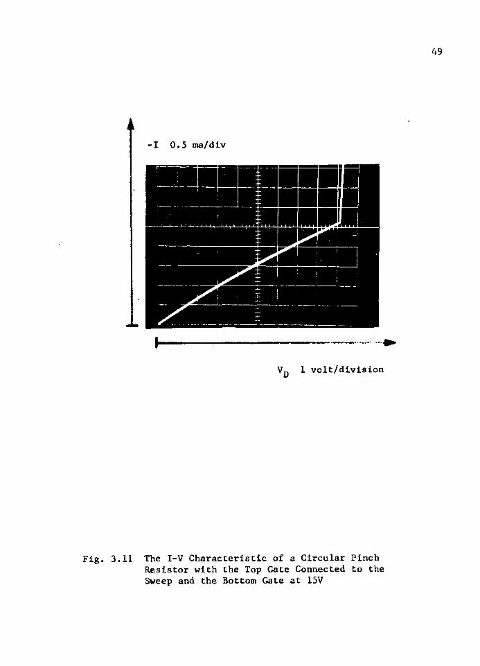
3.11 displays the result. As expected the curve is still fairly straight. The average resistance, however, has increased because of the larger bottom depletion region, due to a larger reverse bias. Such a large reverse bias does not cause breakdown because of the higher breakdown voltage associated with the channel-bottom gate junction, an
effect of lower surface concentration. 'The resistance has increased from 2.7 K, for the previous gate
bias, to 3.44 K.The previous situation was then varied by opening the bottom
gate and applying a positive 8.9 V to the top gate. The resultant I-V characteristic is shown in Fig. 3.12. ...
Once again the resistance is fairly linear over the sweep voltage. The resistance decreases slightly with increasing sweep voltage in contrast to a slightly increasing resistance in the former case. For low sweep values Fig. 3.12 indicates larger resistances than in Fig, 3.9. However, above seven volts the two curves seem to agree more closely.By referring to Fig. 3.13, it can be seen that at large sweep voltages the depletion regions of the two cases are similar, leading to similar resistance. At low voltages, e, the top depletion region is predominant.
The impurity concentration towards the top of the channel is higher than
near the bottom and since the high concentration region, or low resistivity region, is depleted, the current must pass through the bottom of
the channel where the resistance is higher, thus producing a higher resistance at low .sweep voltages than the previous case.
49
I 0.5 ma/div
Vn 1 volt/division
Fig. 3.11 The I-V Characteristic of a Circular PinchResistor with the Top Gate Connected to theSweep and the Bottom Gate at 15V

50
I 0.5 ma/div
V__ 1 volt/division
Fig. 3.12 The I-V Characteristic of a Circular PinchResistor with the Top Gate at 8.9V and theBottom Gate Open

51
8.9Vn top gate
p" channel€
n" bottom gate
(a) Small voltage across the channel
x » r2 x =
n" top gate
8.9V p" channel
n” bottom gate
(b) Large voltage across the channel
Fig. 3.13 Cross Sectional View of a Circular Pinch Resistorwith the Top Gate at 8.9V and the Bottom Gate Open

52
With the inner radius again grounded, the two gates were,alsogrounded and the outer radius was swept with a negative voltage. Figure
I3.14 shows the characteristic.
This arrangement is similar to typical JFET operation as theicurve indicates. The depletion region will increase on top and bottom
near x =» rg as the sweep voltage becomes more negative. The top gate* channel junction breakdown is encountered before sufficient voltage can be applied to pinch the channel off.
Device EvaluationThe wafer was diced and several devices were mounted and bonded
to TO-5 ten pin headers. The two substrate contacts were bonded to the same pin while the top gate was bonded to a separate pin. Upon testing these resistors using a nine volt gate bias, the resistances lay between
2 and 5 Kfi.Parasitic capacitance was the next parameter to be evaluated.
In specifying a capacitance associated with a device, it is helpful to formulate a model whereby the distributed device is approximated by
several discrete resistors and capacitors. A first order model as well
as the circuit symbol for the pinch resistor is shown in Fig. 3.15.The distributed resistance of the channel is lumped into one resistor,R. Two capacitors, and Cg, represent the parasitic capacitance. Ahigher order model can be obtained by connecting similar first order mode Is however, this is unnecessary for the present work.
The testing circuit is shown in Fig. 3.16. By varying thegate voltage, the capacitance as a function of bias voltage can be

1 volt/div
I 0.5 ma/div
3.14 The I-V Characteristic of a Circular Pinch Resistor with Both Gates Grounded and the Outer Radius Swept with a Negative Voltage (All Voltages Relative to the Inner Radius)

54O Drain
Gate
6 Source
(a) Circuit Symbol
Drain
Gate
v Source
(b) First Order Model
Fig. 3.15 Pinch Resistor Circuit Symbol and First Order Model

> +
55
110K
Tektronix 130L-C Meter
Fig. 3.16 Test Circuit Used to Measure Parasitic Capacitance

56
obtained. To obtain an average value of the total capacitance, the parasitic capacitance is measured first with zero bias and then at the maximum bias before breakdown. An average of the two readings is found.This value is divided in half to obtain and Cg.
! Table 3.1 lists the total capacitance of the device at different gate bias levels. At zero volts 140 pf was measured and at eight volts 60 pf was measured. This gives an average of 100 pf. Cj and Cg are 50 pf each. When the resistor is connected with the source and gate at
the same potential, the effective capacitance is 50 pf since is shorted.
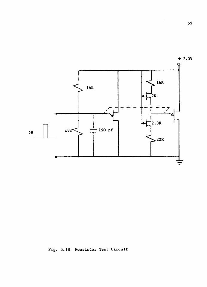
Two pinch resistors were then used to bias a unijunction transis
tor in one of the neuristor lines. Because of the low resistances associated with these devices, two external resistors were also used to make the thevenin resistance larger tlian the negative resistance of the UJT characteristic. The object of this test was to make the unijunction transistor oscillate with just the parasitic capacitance of the pinch
resistors. The UJT can be made to oscillate by increasing the bias voltage until the B.C. load line rises above the peak point of the UJT. The circuit used for this is shown in Fig. 3.17. The UJT oscillated
using these values. The large resistors were necessary and they repre
sent the smallest allowable values for oscillation.These same resistors were then tested in a neuristor line. The
test circuit is shown in Fig. 3.18. Only two unijunction transistors in the neuristor line were connected since the effectiveness; of the pinch
resistors can just as well be demonstrated by having one unijunction

57
Table 3.1PARASITIC CAPACITANCE AS A FUNCTION
OF GATE BIAS VOLTAGE
BIAS VOLTAGE in volts
TOTAL CAPACITANCE in pf
0 1400.5 1 1151 . 0 i 1 0 0
1.5 | 982 . 0 922.5 8 6
3.0 823.5 |1 784.0 754.5 725.0 706 . 0 677.0 638 . 0 || 60

58
+ V + 7.5V
16K
2KUnijunction transistor
in a neuristor line
2.3K
22K
Fig. 3.17 UJT Oscillator Test Circuit
59
+ 7.5V
16K16K
2K
150 pf18K-2V
Fig. 3.18 Neuristor Test Circuit

fire instead of three or four. Both UJT's were biased slightly below
their peak points. Upon triggering" the first unijunction transistor with a two volt positive pulse, the resulting drop in its emitter potential caused the peak point of the second unijunction transistor to drop below its load line. The second unijunction transistor then fired indicating there was sufficient parasitic capacitance in the pinch resis
tors used to bias it.By biasing successive unijunction transistors in the neuristor
line the pulse can be made to fire these elements and propagate farther
down the line.

Chapter 4 CONCLUSION
The results indicate that neuristor biasing can successfully be accomplished using pinch resistors. Pinch resistors can provide the necessary high resistance required as well as sufficient parasitic
capacitance to avoid fabricating additional capacitors.Ultimate design of the pinch resistors depends on the charac
teristics of the accompanying neuristor. If strong coupling between adjacent unijunction transistors exists, small resistors and capacitors will be needed.
If large resistors are required, "dog-bone" resistors can be
connected to circular ones to achieve both high resistance and capaci
tance .
61

Appendix ADERIVATION OF THE CHANNEL CONDUCTANCE
OF A "DOG-BONE" PINCH RESISTOR
In the following derivation the assumptions listed in Chapter 2are used. Pertinent voltages and dimensions of the pinch resistor are
shown in Fig. A.I.As stated in Chapter 2, the thickness of the depletion region in
the channel is given by
[ "<X) ]The voltage necessary to fully deplete the channel is
% • [ ? ] . -
Combining these two equations yields
The undepleted portion of the channel is given by
b(W) = a - Yp(W) = a I* 1 - ( ^ ]
62
(2.2)
(2.4)
(A. 1)
(A.2)

63
y(W)W(x)+ V (x)
b(W)
Fig. A.1 Cross Sectional View of a "Dog-bone” Pinch Resistor Showing the Coordinate System Used to Evaluate the Channel Conductance

64The "yM and "z" component of the field, E, in the undepleted
channel is zero. The current density in the channel is then given by
J « ffEx
In terms of the voltage along the channel, V(x), the current density is
J = tr[ id ^ i ] (A-3)
Since
where
then
I - J • Area
A = 2bZ
I - 2bZ<r ^5 ^ j (A.4)
The dependence on V(x) can be replaced by W(x) by referring to
Fig. A.1 and writing a loop equation.
V(x) - W(x) + VG = 0
Differentiation of this equation with respect to x yieldsdMKi = <Mxi dx dx
The current is then
I = 2bZcr (A.6 )
The current is found in the following manner:

65
dx » 2crZaf-W(L)
W(o ’ [1" 1 1 ](A.7)
Define
:o 52orZaW0
3L
as the pinch off current.The voltages across the depletion region can be expressed in
terms of terminal voltages.
W(o) - Vq
W(L) “ VG - VD
Equation (A.7) can now be expressed as
1 = 1 , 3 I + 2w. w. > )
3/2(A. 8 )
The conductance of the channel is
constant
66
The conductance of the channel is
3 Ip1 - VG - Vi (A.9)
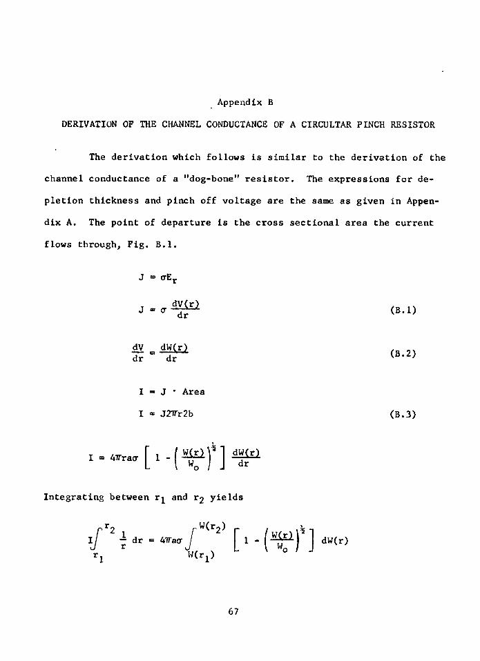
Appendix BDERIVATION OF THE CHANNEL CONDUCTANCE OF A CIRCULTAR PINCH RESISTOR
The derivation which follows is similar to the derivation of the channel conductance of a "dog-bone" resistor. The expressions for depletion thickness and pinch off voltage are the same as given in Appendix A. The point of departure is the cross sectional area the current flows through. Fig. B.l.
J = crEr
(B.l)
dV _ dW(r) dr dr (B.2)
I ” J • AreaI = J2TTr2b (B.3)
I = 4TTracr
Integrating between r^ and rg yields
dr = 47Tacr dW(r)
67

68
DrainDrain GateGateGate Gate Source
2 ap channel
n substrate
Fig. B.l Cross Sectional View of a Circular Pinch Resistor Including Terminal Voltages

69
I *47T ao- WQ
—
3 in ~ rl
3W(r2) 3W(ri) /W(r2 ) \ 3 / 2 /W(r1)w. w. - 2 \ wc / + 2 W,
3/2
(B .4 )
Denoting the inner radius as the source and the outer radius as
the drain, the voltage across the depletion region can be expressed in
terms of the terminal voltages. Fig. B.1.
w<ri> “ VG
W(r2) - VG - VD
Define47T acr W-
3 in
as the pinch off current. The current in the channel is
1 = 1, HiW, - 2 V G " V I
3 /2 Vc\3/2/ (B.5)
The conductance of the channel is then
3Io1 - VG - Vp (B.6)
This expression is similar to that for the "dog-bone” resistor except
for the pinch off current, I0.

LIST OF REFERENCES
Crane, EL D. Neurisfcor Studies. Technical Report No. 1506-2, Solid State Electronics Laboratory, Stanford University, Stanford, California, July 11, 1960.
Grove, A. S. Physics and Technology of Semiconductor Devices. New York: John Wiley and Sons, Inc., 1967.
Hamilton, Douglas J. and Fred A. Lindholm. Introduction to Semiconductor Device Modelling and Applications. New York: Holt, Rinehartand Winston, in press.
Irvin, J. C. "Resistivity of Bulk Silicon and of Diffused Layers inSilicon," Bell System Techn. J.. Vol. 41, March, 1962, 387-410.
Mattson, Roy H. "A Neuristor Realization," Proceedings of the IEEE,Vol. 52, No. 5, May, 1964, 618-619.
Shockley, William. "A Unipolar 1Field-Effect® Transistor," Proc. IRE. Vol. 40, November, 1952, 1365-1376.
Warner, Raymond M., Jr. (ed.). Integrated Circuits: Design Principlesand Fabrication. New York: McGraw-Hill Book Company, 1965.
70
x