investigation of nucleation mechanism and tapering observed in zno
TRANSCRIPT

NANO EXPRESS Open Access
Investigation of Nucleation Mechanism andTapering Observed in ZnO Nanowire Growthby Carbothermal Reduction TechniqueAyan Kar1*, Ke-Bin Low4, Michael Oye5, Michael A Stroscio1,2,3, Mitra Dutta1,2, Alan Nicholls4, M Meyyappan5
Abstract
ZnO nanowire nucleation mechanism and initial stages of nanowire growth using the carbothermal reductiontechnique are studied confirming the involvement of the catalyst at the tip in the growth process. Role of the Aucatalyst is further confirmed when the tapering observed in the nanowires can be explained by the change in theshape of the catalyst causing a variation of the contact area at the liquid–solid interface of the nanowires. The rateof decrease in nanowire diameter with length on the average is found to be 0.36 nm/s and this rate is larger nearthe base. Variation in the ZnO nanowire diameter with length is further explained on the basis of the rate at whichZn atoms are supplied as well as the droplet stability at the high flow rates and temperature. Further, saw-toothfaceting is noticed in tapered nanowires, and the formation is analyzed crystallographically.
IntroductionInterest in nanowires continues to grow fueled by appli-cations in electronics, optoelectronics, sensors, piezo-electric and thermoelectric devices, and energy storage[1]. In spite of considerable advances in growth andapplication development of nanowires, the various pro-posed growth mechanisms are still controversial andsubject to immense discussion. For example, it is welldocumented that the diameter of nanowires grown viathe vapor–liquid–solid (VLS) mechanism is determinedby the size of the droplet. This is true but it does notnecessarily imply that the diameter of nanowires is con-stant along its axis. It has been recently reported thatthe dynamic reshaping of the catalyst particles duringthe nanowire growth determines the length and shapeof the nanowires [2]. Also, just as in elemental semicon-ductors [3], there is a general consensus that even foroxide nanowires the whole molten alloy particle,referred to as the catalyst, rises above the surface of thesubstrate and rides at the tip of the nanowire during thegrowth process. The objective of this paper is twofold.First, we investigate the initial stages of nucleation, oxi-dation of Zn atoms, and growth of ZnO nanowires.
Secondly, we investigate the formation of tapered nano-wires from the growth kinetics point of view. Comparedto elemental and III–V nanowires, growth behavior ofsemiconducting oxide nanowires, and in particular ZnOis not well understood [1]. ZnO has been proven to bequite a complex and interesting material with a varietyof structures such as nanowires, nanobelts, and tetra-pods [4]. Each of these structures can be formed by dif-ferent growth mechanisms under widely differentthermodynamic conditions. The recent surge in applica-tions of ZnO nanowires as a piezoelectric material [5]for energy harvesting has led to the present investiga-tion. The dependence of nanowire diameter on theamount of generated piezoelectricity requires clarifica-tion of the role of gold at the nanowire tip in control-ling the shape and diameter of the nanowire [6].
Experimental WorkThe source consists of zinc oxide (ZnO) metal basis of99.999% purity mixed with graphite in a weight ratio of1:1 to carry out a carbothermal reduction process. A 1″diameter quartz tube was inserted inside an isothermalfurnace, and the source mixture was kept in a quartzboat inside this tubular reactor. Gold colloids were usedas the catalyst for different experiments. The substratewith the Au catalyst was placed downstream from thequartz boat located at the center of the heating zone.
* Correspondence: [email protected] and Computer Engineering Department, University of Illinois,Chicago, IL 60607, USA.Full list of author information is available at the end of the article
Kar et al. Nanoscale Res Lett 2011, 6:3http://www.nanoscalereslett.com/content/6/1/3
© 2010 Kar et al. This is an Open Access article distributed under the terms of the Creative Commons Attribution License(http://creativecommons.org/licenses/by/2.0), which permits unrestricted use, distribution, and reproduction in any medium,provided the original work is properly cited.

One end of the quartz tube was connected to a massflow controller, which controls the flow rate of the car-rier gas, argon, and the other end was connected to theexhaust. Nanowires were grown within a temperaturewindow of 900–980°C, whereas the carrier gas flow ratewas varied between 100–160 sccm.Fifty nanometres Au colloids (BBI International) were
used as the starting catalyst. The c-sapphire substratewas treated with poly-L-Lysine before dropcasting theAu colloidal solution. The substrate was then spun at2000 rpm for 1.5–2 min ensuring a random dispersionof the gold particles. The flow rate of Ar carrying theZn vapor was maintained at 100 sccm and turned ononly for the duration of growth after the temperaturewas allowed to stabilize at 900°C. At the synthesis tem-perature, carbothermal reduction of the ZnO powderyields Zn vapor according to the following reactions:
Carbothermal Reduction source
ZnO C Zn CO
( )+ → +
:
( ) ( ) ( ) ( )s s v g(1)
Catalystalloy formation Zn Au Au Zn: ( ) ( ) ( )v s l+ → − (2)
Results and DiscussionFigure 1a shows the SEM image of the substrate surfaceafter the gold nanoparticles were exposed to the ZnO:Csource at 900°C for t = 90 ± 10 s. In the initial stages oftemperature ramping, the substrate becomes coveredwith Au islands, which become the preferential sites forZn incorporation. The Zn atoms can either condensefrom the vapor phase or be transferred from adjacentregions of the substrate. Then, they rapidly diffuse intothe Au clusters forming the Au–Zn clusters. The Znconcentration in these particles increases with time,until a solid crystal nucleates out of the alloy dropletdue to supersaturation in the droplet. SEM-EDX wasperformed in order to investigate the islands seen inFigure 1a, b and to gain further insight about thenucleus formation. Figure 2a shows a SEM image of thesubstrate surface after t = 90 ± 10 s. The EDS measure-ment was performed on points A and B of the island inFigure 2a, and the acquisition time was 120 s. Themajor signals from EDS are O (Ka) at 0.524 keV, Au(Ma) at 2.1 keV, and Zn (La) at 3.4 keV using a 20 kVelectron beam. The data obtained shows that the island(point A) has a greater concentration of Zn comparedto Au. With increasing amount of Zn condensation anddissolution from the source vapor, Zn and Au form analloy and liquefy giving rise to the islands on the sub-strate. This leads to an increase in the volume of thealloy droplet as more Zn is carried to the droplet anddissolves. The process of Zn dissolution into the alloy
continues till the ratio of Zn in the Au–Zn alloyincreases beyond a certain thermodynamic limit, leadingto the formation of the nucleus. In contrast to theislands, the nucleus has more Au compared to Zn as inthe EDX for point B. This is further confirmed by theSTEM-XEDS elemental mapping of a single ZnO wire(see Figure 2d), which shows a high Au concentration(yellow) in the catalyst at the tip of the nanowire. As Zncontinues to further condense/dissolve into the nucleus,precipitation of the ZnO nanowire would start under-neath this nucleus with Au-dominated nucleus riding ontop of the nanowire as catalyst. Hence, the Au/Zn ratiois found to vary from the islands remaining on the sub-strate to the nucleus that becomes the catalyst riding ontop of the wire.Formation of a crystal nucleus from the liquid Zn–Au
metal droplet (schematic of which is shown later inFigure 4a) leading to nanowire growth is shown in twostages in Figure 1b, c for t = 90 ± 10 and 120 ± 10 s,respectively. Thermodynamically, Gibbs free energyminimization is the criterion to be satisfied for the for-mation of the nucleus. After the nucleus is formed, ZnOnanowires start to form, as shown in Figure 1d, e for t =18 ± 1 min and 20 ± 0.5 min, respectively, with the cat-alyst at the tip which acts as the sink for the Zn atomsand generates a concentration gradient along the cata-lyst particle. However, the Zn–Au alloy droplet onwhich the nuclei forms remains on the substrate. Thenanowire formation can be described by the followingreaction
Nanowire growth: Au Zn Zn O
Au Zn ZnO
− + +→ − +
( ) ( ) /
( ) ( )
l v
l s
1 2 2 (3)
The oxidation process of the Zn leading to the forma-tion of ZnO contributing to the nanowire growth is acritical step. In the present case, it is likely that ZnOnanowires originate from the oxidation of the Zn atomswithin the Au–Zn alloy particle since it is commonlyknown that the activity of metals can be increased uponalloying. It has been previously reported that the oxida-tion of alloys such as Zn–Ag and Zn–Cu results in theformation of ZnO crystalline precipitates [7]. In a simi-lar manner, it is believed ZnO will precipitate in theform of ZnO nanowires due to the oxidation of Au–Znparticles. There have also been recent claims statingthat there is no involvement of a liquid or solid catalystat the tip of ZnO nanowires in the growth processinvolving thermal evaporation [8]. The SEM images inFigures 1d, e and 2d here show a distinct catalyst at thenanowire tip that serves to control the diameter of thenanowire.We propose here that Zn atoms are the main species
contributing to crystal growth and not ZnO. The gold
Kar et al. Nanoscale Res Lett 2011, 6:3http://www.nanoscalereslett.com/content/6/1/3
Page 2 of 9

particles alloy with Zn and the oxide nanowires growwith the assistance of the liquid catalyst particles at thewire tip where the Zn atoms are oxidized, as discussedpreviously. Since the ZnO crystal nucleates at the solid–liquid interface, the nanowire diameter is determinedand controlled by the size of the gold catalyst droplet atthe tip, which is a feature common in VLS process [1,9].We also point out contradicting reports [10] whereinnanowire branches with substantially different diameterscompared to the catalyst particle have been seen; agrowth mechanism different from VLS was suggested,and ZnO atoms were believed to be the source of nano-wire growth instead of Zn atoms.The shape of the semiconductors at the nanoscale is
another decisive factor for the properties, and the shapecontrolled growth of semiconductors can find uniqueapplications in electronics and photonics. Until now,tapered ZnO nanowires have only been produced bychemical synthesis or electrochemical deposition
method [11]. Here, we report the observation of taperedZnO nanowires grown using the carbothermal reductionmethod in a furnace. Figure 3a shows nanowires with auniform diameter throughout their axis, grown onp-type silicon substrates at a temperature of 900°C andargon flow rate of 100 sccm. Tapered nanowires areformed at a growth temperature of 980°C and an Arflow rate of 160 sccm as seen in Figure 3b–e. Thegrowth times were 10 min for Figure 3b, c and 25 minfor Figure 3d, e. At a lower flow rate of 140 sccm butat the same temperature of 980°C, nanowires with justa tapered base but uniform long stems are seen inFigure 4b. The illustration in Figure 4a is used in orderto understand the tapering mechanism. To put thingsinto perspective, the growth of tapered nanowires canbe categorized as a special case of cylindrical nanowireswith the flank angle δ = 0. In fact, diameters of epitaxi-ally grown Si nanowires have been shown [12] to vary,especially in the region close to the substrate where the
Figure 1 a and b show the Au–Zn clusters with the nucleation sites formed on the substrates. c Early stage of nanowire nucleation fromthe Au–Zn clusters. d and e show eventual wire formation with the presence of the catalyst at the nanowire tip (also shown as inset in fig e).Scales in figure (a), (d), and (e) are 2 μm, whereas in figures (b) and (c), the scale is 500 nm and 200 nm, respectively.
Kar et al. Nanoscale Res Lett 2011, 6:3http://www.nanoscalereslett.com/content/6/1/3
Page 3 of 9

nanowires exhibit larger diameters just as seen here forZnO nanowires in Figures 3b–e and 4b. One first guesswould be that this large diameter is created by radialovergrowth of the nanowire after axial growth. Espe-cially at elevated temperatures, surface diffusion andvapor–solid growth might influence the shape and resultin enlargement of the nanowire base. In particular, afaceting of the nanowire base expansion, often observedat high temperatures, might occur after growth bysurface diffusion. Such faceting of the base is seen inFigure 4b as indicated by arrows.The illustration in Figure 4a shows that the decrease
in nanowire diameter along its length is controlled bythe size of the catalyst contact area at the liquid–solidinterface. In our case, the angle a equals to zero at thebeginning stages of nucleation. As growth begins, theangle a has to increase, which is accompanied by anincrease in the contact angle b based on a modifiedYoung’s equation [12]:
l s ls Rcos( ) cos( )= − − (4)
which means that the droplet approaches a larger solidangle of spherical section. Here, sl, sls, and ss are thesurface tension of the droplet surface, the liquid–solidinterface, and the solid, respectively. The droplet at the
tip of the nanowire has a contact area of radius R and τ isthe line tension. The increase in the contact angle bcauses a decrease in the contact area and a decrease inthe radius R of the droplet. Consequently, the radius ofthe nanowire R should be smaller than the initial radiusr′ of the contact area of the nuclei on the Au–Zn droplet.Thus, the nanowire diameter is largest at the base anddecreases as the length of the wire increases, with thediameter being directly controlled by the shrinking radiusof the contact area R at the droplet tip. The average rateof decrease in the nanowire diameter with time (taperingrate) for needle-like nanowires here is estimated as0.36 nm/s and plotted in Figure 4d. Also, plotted is thegrowth rate of the nanowires, and the average ratethroughout the process is estimated as 3.9 nm/s. How-ever, the growth rate is relatively slower at the onset ofgrowth and speeds up with time. The decrease in dia-meter of the nanowire with length of both needle-likenanowires and the ones with just tapered bases areplotted in Figure 4c. The rate of decrease in diameter ismuch larger close to the base and then decreases as thelength increases. This can be explained by the fact thatthe rate of increase of angle a with length is large closeto the base of the nanowire and decreases gradually.Thus, one reason for the decrease in nanowire diameterwith length, i.e. tapering, is the reduction in the size ofthe catalyst at the tip as growth progresses.
Figure 2 a SEM image of the Au–Zn nucleation sites formed on the substrates at early stages of growth. b and c SEM-EDX done onpoint A and point B as marked in figure (a). d shows STEM elemental spectral analysis done on an individual nanowire.
Kar et al. Nanoscale Res Lett 2011, 6:3http://www.nanoscalereslett.com/content/6/1/3
Page 4 of 9

Nanowires of two different morphologies are recalledhere: in one case, we have the tapering just restricted tothe base, as seen in Figure 4b, and another where wesee a continuous decrease in nanowire diameter withlength, as in Figure 3b–e; both morphologies can beexplained on the basis of the rate at which the Znatoms are deposited/delivered to the substrate if thetemperature is kept constant. The concentration of theZn adatoms at the substrate will increase as the Ar car-rier gas flow rates are increased. Due to the concentra-tion gradient between the substrate surface and thenanowire, diffusion of the adatoms becomes prominentat flow rates >140 sccm. Excess growth species are avail-able at the base of the ZnO nanowire, where the mobi-lity of Zn atoms diffusing from the substrate surface tothe nanowire tip is impeded and allows radial taperingof the base [13]. The base diameter thus increases stea-dily with an increase in flow rates. This gives riseto tapered, as in Figure 4b, but not needle-shaped
nanowires, as in Figure 3. Further, it is to be noticedthat the tapered segment of the nanowire in Figure 4b isvery small. This is probably due to the limitation of ada-tom diffusion via the nanowire sidewall, since theupward adatom mobility via the nanowire sidewallsdecreases at high temperatures [14]. However, as theflow rates are increased further, the tapered nanowiresgive way to needle-like nanowires, obtained in this caseat a flow rate of 160 sccm as shown in Figure 3b–ewhere there is a constant decrease in diameter withlength. Such observations have been reported previouslyin the growth of InAs nanowires [13]. The tapering alsoindicates that adatom surface diffusion from the sub-strate up the nanowire sidewalls forms a path for thegrowth species reaching the alloy droplet other than thedirect impingement of the atoms on the droplet, as hasbeen reported previously [13]. A theoretical study [15]investigating the shape of the nanowires on the basis ofthe contact angle b of the liquid droplet at the nanowire
Figure 3 a ZnO nanowires with uniform diameters grown on p-type Si (100) substrates. b–d show nanowires with a constant decrease indiameter along the axis grown at a higher flow rate and temperature. The growth time for figures (b) and (c) were 10 min and that for figures(e) and (f) were 25 min. Scales in all the figures are 2 μm.
Kar et al. Nanoscale Res Lett 2011, 6:3http://www.nanoscalereslett.com/content/6/1/3
Page 5 of 9

tip found surprisingly that tapered nanowire growth (∂ > 0)is more likely for a wide range of contact angles b com-pared to nanowires with uniform diameters.The tapering of the nanowires can also be explained on
the basis of the stability and shape of the Au catalyst atthe tip of the nanowires. Nanowires with uniform dia-meters, seen in Figures 1 and 3a, are formed when thegrowth species land at a constant rate on the droplet, andthe droplet is sufficiently stable (when surface tension >stress) at the growth temperature to resist decay or disin-tegration and hence maintaining its spherical shape.However, it has been noted previously [16] that hightemperatures and flow rates cause droplet instability,which may be one of the reasons for the continuousdecrease in nanowire diameter with length. Mohammadreported [16] that high temperatures and flow rates causethe Au particle at the tip of the nanowire to lose its sphe-rical shape indicating an unstable droplet. This dropletinstability leading to the formation of tapered nanowiresis clearly seen in Figure 5, which compares the shape ofthe catalyst at the tips of tapered (Figure 5a) and straight(Figure 5b) nanowires. The catalyst at the tip of thetapered nanowire has an ellipsoidal/triangular kind of
shape, whereas the straight nanowire still maintains ahemispherical particle shape. It appears that the catalystin the tapered wire is elongated along the axial direction,and it is not clear whether this elongation is an inter-mediate state of the particle during the course of theshrinking or if it represents some quasi-equilibriumshape at the experimental temperature and flow rate.Figure 5c shows a representative straight wire with itscorresponding diffraction pattern, which also reveals a
zone axis of 2110⎡⎣ ⎤⎦ . The catalyst particle can also be
seen at the end of the wire, which is spherical in shape.For the straight wire, the growth is in the [0001] direc-tion, with both edges of the wires possibly bounded by
the 0110( ) plane. Figure 5d shows TEM images of the
straight and tapered wires where the straight wire isfound to be growing along the c-axis, whereas the tapered
wire along the 0110⎡⎣ ⎤⎦ direction.Oversupply of source vapor as well as interplay of
surface energies of the wire and liquid droplet was alsoreported to cause the droplet to be unstable, leading tooscillations in resulting Si NW structures [17]. This is
Figure 4 a Schematic of the nucleus formed on the molten Au–Zn droplet and ZnO nanowire growth at initial stages with tapering.b ZnO nanowires with tapered base and uniform long stems. c Plot of nanowire diameter vs. length for both tapered and needle-like ZnOnanowires. d Plot showing growth and tapering rates of needle-like ZnO nanowires.
Kar et al. Nanoscale Res Lett 2011, 6:3http://www.nanoscalereslett.com/content/6/1/3
Page 6 of 9

seen here in the case of the tapered ZnO wire inFigure 5d, and such oscillations of the droplet resultingin faceting in the nanowire sidewalls is discussed belowin detail. To our knowledge, this is the first observa-tion of periodic saw-tooth faceting in ZnO nanowires;the observed faceting is periodic, where the period Pof the facets is about 19.2 nm on average and theheight H is about 4 nm. Incidentally, such faceting isobserved only in tapered nanowires and not in straightones as seen in Figure 5d, indicating such facetingmight have some relation to the tapering mechanismobserved in our case.Figure 6a shows a tapered wire and its electron diffrac-
tion pattern, which indicates that it is mono-crystalline.
The zone axis of the diffraction pattern is the 2110⎡⎣ ⎤⎦of the hexagonal ZnO. The base of these tapered wiresvaries greatly from half a micron to a few microns in size.However, it is important to stress that TEM observations
may not provide an accurate estimation of the wiredimensions due to the nature of sample preparation.Although the lateral sizes of these wires are in the sub-micrometer scale, they still possess moderate degree ofelectron transparency at low magnification, indicatingthat these wires have somewhat plate-like morphology.In other words, the widths of these wires are in the sub-micron length scale; if the wires are hypothesized to havethicknesses similar to their widths, then there will be noelectron transparency even in a 300 kV TEM. Given thatatomic resolution was observed on these wires, the wirethicknesses must be in the range of few tens of nan-ometers, which means they are thin and wide (plate-like).The tapered wire in Figure 6a reveals saw-toothed
morphology only on one of the edges, while the otheredge is atomically smooth. According to its diffractionpattern, the smooth edge of the wire is running along
the 0110⎡⎣ ⎤⎦ direction, and it is hypothesized that this
Figure 5 TEM images of (a) tapered ZnO nanowires (b, c) nanowire with uniform diameter, inset in figure c shows diffraction pattern.(d) TEM image of straight and tapered nanowires indicating the growth directions.
Kar et al. Nanoscale Res Lett 2011, 6:3http://www.nanoscalereslett.com/content/6/1/3
Page 7 of 9

edge is exposing the {0002} plane. High-resolutionimages taken from another tapered wire Figure 6b con-firms that the saw-toothed morphology is representative.Figure 6b inset shows the location on the tapered wirefrom which the high-resolution images were obtained.Note that the catalyst particle (darker contrast) is stillintact on the tapered wire. Figure 6b shows that thesaw-toothed edge consists of two predominant types ofplanes: the terraces, which are parallel to the smoothedge, are exposing the (0002) plane; the steps, whichconsistently make an angle of 62.3° (theoretical: 61.4°)
with the (0002), are exposing the 0110( ) plane. It is
important to note that strong lattice fringes are onlyvisible at the tapered, saw-toothed edge, suggesting that
the wire’s cross-section is not uniform but actuallywedge-like, thinning toward the tapered, saw-toothededge. Based on the observed preferential exposure of the
{0002} and 0111{ } -type planes in the hexagonal ZnO
crystal, a model in Figure 7 was constructed to describethe growth of the tapered wire in relation with its crys-tallographic orientation. We have seen that steps expos-
ing the 0111( ) plane help mitigate the tapering along
the edge of the wire. Given that there are other crystal-
lographically equivalent 0111{ } planes in the hexago-
nal system, the model proposes that atomic-scale stepsshould also exist on the top and bottom surfaces of thewire. The possible step configurations are illustrated in
the diagram: (1) pure 1101( ) steps and (2) 1101( )steps with (0002)/ 0111( ) kinks. Indeed, the orienta-
tions of the ‘kinks’, indicated in Figure 6d, agree qualita-tively with the proposed step configurations on thesurfaces of these wires.One mechanism that could lead to such faceting is
surface reconstruction due to charge stabilization inpolar compounds. ZnO crystal is formed by alternatingstacks of oppositely charged O2- and Zn2+ planes paral-lel to the surface. If the resulting dipole moment per-pendicular to the surface is nonzero, stabilization ofsuch a surface is accomplished by a rearrangement ofsurface charges or by introducing compensating chargesinto the outermost surface planes [18]. This could leada significant modification of the surface geometric struc-ture and stoichiometry. The stabilization mechanism forthe Zn-terminated face of ZnO has been experimentallyinvestigated by a variety of techniques, and variousmechanisms have been proposed for the reduction inthe surface charge density to yield a stable Zn termina-tion. Recent experimental studies [19] combinedwith theoretical calculations [20] suggest that theZn-terminated surface can be stabilized by a reconstruc-tion involving triangular surface structures [21]. How-ever, due to the unstable nature of the catalyst at thewire tip, it is believed here that faceting due to dropletoscillation is the dominant mechanism that causes thesurface reconstructions. The observations seen here canbe explained based on a thermodynamic model usedearlier to explain similar faceting in Si nanowires [17].The allowed facets correspond to a wire that is wideningor narrowing as it grows. The wire widens as the dropletis stretched thinner and contact angle b (Figure 4a)decreases, which generates an inward force favoring theintroduction of the narrowing facet. Conversely, the nar-rowing of the wire leads to the droplet applying an
Figure 6 a and b shows TEM and HRTEM images of saw-toothfaceting observed in tapered nanowires, respectively.
Kar et al. Nanoscale Res Lett 2011, 6:3http://www.nanoscalereslett.com/content/6/1/3
Page 8 of 9
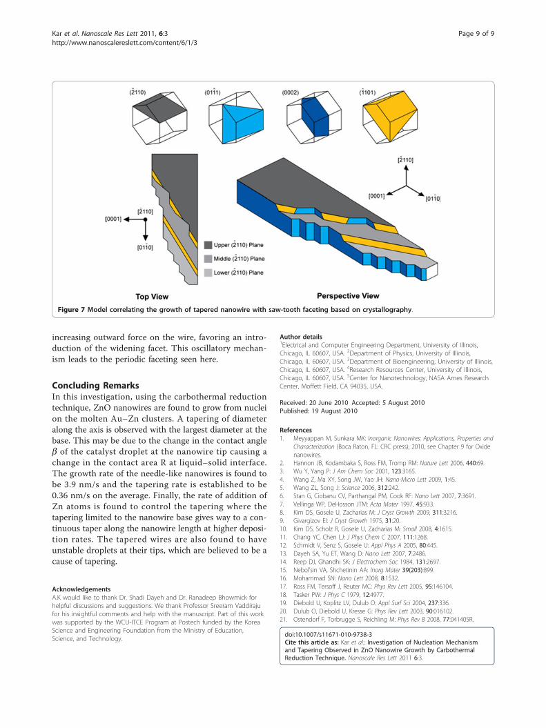
increasing outward force on the wire, favoring an intro-duction of the widening facet. This oscillatory mechan-ism leads to the periodic faceting seen here.
Concluding RemarksIn this investigation, using the carbothermal reductiontechnique, ZnO nanowires are found to grow from nucleion the molten Au–Zn clusters. A tapering of diameteralong the axis is observed with the largest diameter at thebase. This may be due to the change in the contact angleb of the catalyst droplet at the nanowire tip causing achange in the contact area R at liquid–solid interface.The growth rate of the needle-like nanowires is found tobe 3.9 nm/s and the tapering rate is established to be0.36 nm/s on the average. Finally, the rate of addition ofZn atoms is found to control the tapering where thetapering limited to the nanowire base gives way to a con-tinuous taper along the nanowire length at higher deposi-tion rates. The tapered wires are also found to haveunstable droplets at their tips, which are believed to be acause of tapering.
AcknowledgementsA.K would like to thank Dr. Shadi Dayeh and Dr. Ranadeep Bhowmick forhelpful discussions and suggestions. We thank Professor Sreeram Vaddirajufor his insightful comments and help with the manuscript. Part of this workwas supported by the WCU-ITCE Program at Postech funded by the KoreaScience and Engineering Foundation from the Ministry of Education,Science, and Technology.
Author details1Electrical and Computer Engineering Department, University of Illinois,Chicago, IL 60607, USA. 2Department of Physics, University of Illinois,Chicago, IL 60607, USA. 3Department of Bioengineering, University of Illinois,Chicago, IL 60607, USA. 4Research Resources Center, University of Illinois,Chicago, IL 60607, USA. 5Center for Nanotechnology, NASA Ames ResearchCenter, Moffett Field, CA 94035, USA.
Received: 20 June 2010 Accepted: 5 August 2010Published: 19 August 2010
References1. Meyyappan M, Sunkara MK: Inorganic Nanowires: Applications, Properties and
Characterization (Boca Raton, FL: CRC press); 2010, see Chapter 9 for Oxidenanowires.
2. Hannon JB, Kodambaka S, Ross FM, Tromp RM: Nature Lett 2006, 440:69.3. Wu Y, Yang P: J Am Chem Soc 2001, 123:3165.4. Wang Z, Ma XY, Song JW, Yao JH: Nano-Micro Lett 2009, 1:45.5. Wang ZL, Song J: Science 2006, 312:242.6. Stan G, Ciobanu CV, Parthangal PM, Cook RF: Nano Lett 2007, 7:3691.7. Vellinga WP, DeHosson JTM: Acta Mater 1997, 45:933.8. Kim DS, Gosele U, Zacharias M: J Cryst Growth 2009, 311:3216.9. Givargizov EI: J Cryst Growth 1975, 31:20.10. Kim DS, Scholz R, Gosele U, Zacharias M: Small 2008, 4:1615.11. Chang YC, Chen LJ: J Phys Chem C 2007, 111:1268.12. Schmidt V, Senz S, Gosele U: Appl Phys A 2005, 80:445.13. Dayeh SA, Yu ET, Wang D: Nano Lett 2007, 7:2486.14. Reep DJ, Ghandhi SK: J Electrochem Soc 1984, 131:2697.15. Nebol’sin VA, Shchetinin AA: Inorg Mater 39(203):899.16. Mohammad SN: Nano Lett 2008, 8:1532.17. Ross FM, Tersoff J, Reuter MC: Phys Rev Lett 2005, 95:146104.18. Tasker PW: J Phys C 1979, 12:4977.19. Diebold U, Koplitz LV, Dulub O: Appl Surf Sci 2004, 237:336.20. Dulub O, Diebold U, Kresse G: Phys Rev Lett 2003, 90:016102.21. Ostendorf F, Torbrugge S, Reichling M: Phys Rev B 2008, 77:041405R.
doi:10.1007/s11671-010-9738-3Cite this article as: Kar et al.: Investigation of Nucleation Mechanismand Tapering Observed in ZnO Nanowire Growth by CarbothermalReduction Technique. Nanoscale Res Lett 2011 6:3.
Figure 7 Model correlating the growth of tapered nanowire with saw-tooth faceting based on crystallography.
Kar et al. Nanoscale Res Lett 2011, 6:3http://www.nanoscalereslett.com/content/6/1/3
Page 9 of 9