investigations on structural, electrical and optical...
TRANSCRIPT

SDU Journal of Science (E-Journal), 2014, 9 (1): 150-162 ______________________________________________________
150
Investigations on Structural, Electrical and Optical Properties of Polycrystalline CdInTe Thin Films Grown by Thermal
Evaporation
Koray Yılmaz1,*, Deniz Gölcür1
1Pamukkale University, Arts and Science Faculty, Department of Physics, 20020 Denizli, Turkey. *Corresponding author e-mail: [email protected]
Received: 21 March 2014, Accepted: 25 April 2014
Abstract: In this study, properties of thermally evaporated polycrystalline CdInTe thin films were investigated. The surface morphology, composition and crystal structure of the films were determined by means of SEM, EDXA and XRD analysis. Temperature dependent Hall effect measurements were carried out in the temperature range of 200-400 K. In the whole temperature region, the dominant transport mechanism of the films was found to be thermionic emission of the carriers over the grain boundaries. The room temperature conductivity, mobility and electron concentration values were found to be 1.8x10⁻² (Ω.cm)-1, 50 cm2V-1s-1 and 1.1x10⁻¹⁵ cm-3, respectively. The mobility-temperature dependence showed that ionized impurity, neutral donor impurity and acoustic phonon scattering mechanisms were effective over the low (216-256 K), intermediate (256-317 K) and high temperature (317-357 K) regions, respectively. The optoelectronic properties of the films were also investigated by absorption in 190-1100 nm wavelength region and photoconductivity measurements in 80-400 K temperature range. Key words: Semiconductors, thin films, thermal evaporation, Hall effect
Termal Buharlaştırma ile Büyütülmüş Polikristal CdInTe İnce Filmlerin Yapısal, Elektriksel ve Optik Özelliklerinin
Araştırılması
Özet: Bu çalışmada, termal buharlaştırma yoluyla üretilmiş polikristal CdInTe ince filmlerin özellikleri araştırılmıştır. Filmlerin yüzey morfolojisi, kompozisyonu ve kristal yapısı SEM, EDXA ve XRD analizleri ile incelenmiştir. Sıcaklığa bağlı Hall etkisi ölçümleri 200-400 K sıcaklık aralığında gerçekleştirilmiştir. Tüm sıcaklık aralığında etkin akım mekanizmasının termoiyonik emisyon olduğu tespit edilmiştir. Oda sıcaklığında iletkenlik, mobilite ve elektron konsantrasyonu sırasıyla 1.8x10⁻² (Ω.cm)-1, 50 cm2V-1s-1 ve 1.1x10⁻¹⁵ cm-3 olarak bulunmuştur. Mobilite-sıcaklık değişimi ölçümlerinden iyonize safsızsızlık, nötral verici safsızlığı ve akustik fonon saçılma mekanizmalarının sırasıyla (216-256 K), (256-317 K) ve (317-357 K) sıcaklık aralıklarında etkin olduğu belirlenmiştir. Filmlerin optoelektronik özellikleri 190-1100 nm dalgaboyu aralığında soğurma ve 80-400 K sıcaklık aralığında fotoiletkenlik ölçümleri ile araştırılmıştır. Anahtar kelimeler: Yarıiletken, ince film, termal buharlaştırma, Hall etkisi 1. Introduction In the last decade, II-VI compounds have been intensively investigated due to their applications in optoelectronics and photovoltaic industry [1-4]. CdTe is one of the most studied compounds of this family since it has a suitable band gap around 1.5 eV for solar energy conversion [5-8]. This compound generally crystallizes in the cubic or hexagonal system and has a defective chalcopyrite structure [4, 9, 10]. Besides II-VI compounds, ternary II-III2-VI4 compounds such as CdIn2Te4 has taken considerable attention in recent years. Growth of CdInTe films on glass substrates using close-space vapor transport combined with the free evaporation technique (CSVT-FE) has given

K. Yılmaz, D. Gölcür
151
opportunities for large area applications that is required for solar energy conversion. Optoelectronic properties of CdInTe films grown by CSVT-FE technique were studied for different indium concentrations by Iribarren et. al [11]. It has been reported that as-grown CdTe films by the CSVT-FE technique are normally rich in Cd vacancies which results in p-type conduction. This is one of the reasons that limit its usage in solar cell applications. When indium atoms are introduced into the lattice of CdTe, they could fill Cd vacancies and/or substitute the Cd atoms in the structure. Thus, this compensation of such vacancies results in n-type conduction. Even though In doped CdTe and CdIn2Te4 compounds have been widely studied by various researchers [12-16], studies on electrical transport, scattering mechanisms and photoconductive properties of as-grown CdInTe polycrystalline films deposited by thermal evaporation method were not extensively reported in literature. Thus, the main aim of this work is to investigate structural, optical and electrical properties of thermally evaporated as-grown polycrystalline CdInTe thin films for a possible application of optoelectronic devices. 2. Material and Methods In order to obtain evaporation source, stoichiometric quantities of high purity (4Ns) Cd, In and Te elements have been placed into a chemically cleaned quartz ampoule. The ampoule was evacuated and sealed under a pressure of about 10-4 Torr. Then, the ampoule was placed in a horizontal, constant temperature zone furnace and heated gently, avoiding over pressures, up to a temperature 1200 oC (1473 K) higher than the melting points of the elements during 48 hrs and then cooled very slowly (10-15 oC/h). In order to achieve homogeneity, the ampoule was stirred occasionally during the heating process. Evaporation source was obtained by crushing the resulting ingot into fine grains. CdInTe thin films having thicknesses around 0.5 µm were deposited on chemically and ultrasonically cleaned glass substrates by thermal evaporation technique using a molybdenum boat. A vacuum of 10-6 Torr was maintained during the time of deposition with around 20-25 Ao/s deposition rate which was controlled by Inficon XTM/2 thickness monitor. Several set of samples were produced in order to achieve film reproducibility. The surface morphology and composition of the films were investigated by JEOL (JSM-7600F) model scanning electron microscope (SEM) equipped with energy dispersive X-ray analysis (EDXA) facility, operated at 15 kV. X-ray diffraction measurements were taken at scan speed of 0.01o/s by using a Rigaku (SmartLab) XRD system equipped with Cu Kα radiation source. For the electrical measurements, ohmic contacts were achieved by thermal evaporation of high purity indium through a mask in Van der Pauw geometry. Then, copper wires attached to the contacts with silver paste. The ohmicity of the contacts was checked during the dark current-voltage measurements at different temperatures to make sure that the contacts did not add any parasitic impedance to the samples beyond the equilibrium values. The temperature-dependent conductivity and Hall Effect measurements were carried out in a Janis closed cycle helium cryostat in the temperature range of 200-400 K by using a Keithley 2400 programmable source-measure unit and a Keithley 2700 electrometer equipped with a Keithley 7709 matrix card. For the Hall measurements a magnetic field of 1.2 Tesla was applied perpendicular to the layers by using a GMW electromagnet and the temperature was accurately monitored with a Lake-Shore 320 temperature controller. Optical absorption measurements were carried out with a Unico SQ 2802 UV/VIS spectrophotometer over the wavelength range of 190-1100 nm. Temperature
SDU Journal of Science (E-Journal), 2014, 9 (1): 150-162 ______________________________________________________
152
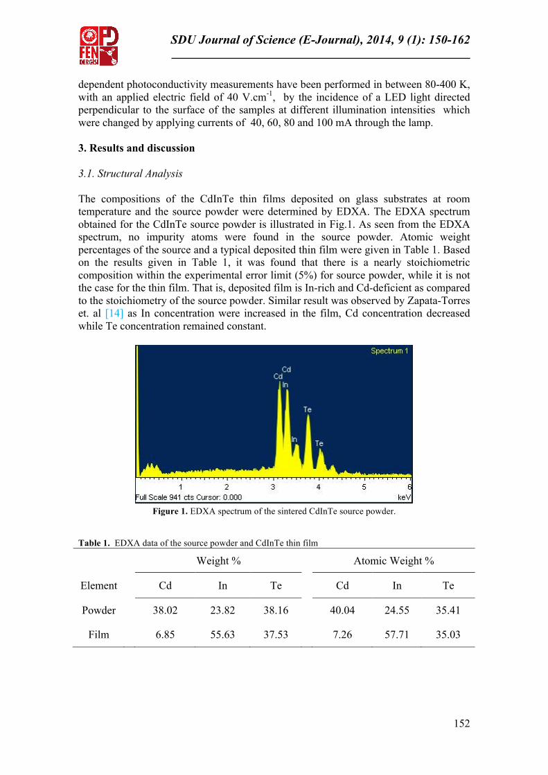
dependent photoconductivity measurements have been performed in between 80-400 K, with an applied electric field of 40 V.cm-1, by the incidence of a LED light directed perpendicular to the surface of the samples at different illumination intensities which were changed by applying currents of 40, 60, 80 and 100 mA through the lamp. 3. Results and discussion 3.1. Structural Analysis The compositions of the CdInTe thin films deposited on glass substrates at room temperature and the source powder were determined by EDXA. The EDXA spectrum obtained for the CdInTe source powder is illustrated in Fig.1. As seen from the EDXA spectrum, no impurity atoms were found in the source powder. Atomic weight percentages of the source and a typical deposited thin film were given in Table 1. Based on the results given in Table 1, it was found that there is a nearly stoichiometric composition within the experimental error limit (5%) for source powder, while it is not the case for the thin film. That is, deposited film is In-rich and Cd-deficient as compared to the stoichiometry of the source powder. Similar result was observed by Zapata-Torres et. al [14] as In concentration were increased in the film, Cd concentration decreased while Te concentration remained constant.
Figure 1. EDXA spectrum of the sintered CdInTe source powder.
Table 1. EDXA data of the source powder and CdInTe thin film
Weight % Atomic Weight %
Element Cd In Te Cd In Te
Powder 38.02 23.82 38.16 40.04 24.55 35.41
Film 6.85 55.63 37.53 7.26 57.71 35.03

K. Yılmaz, D. Gölcür
153
The surface morphology of the films was analyzed using a scanning electron microscope (SEM), which is a convenient technique to study the microstructure of thin films. In Fig.2, SEM picture of a typical film is presented at magnification of 20,000x.
Figure 2. SEM Picture of the CdInTe thin film. It can be observed from the picture that the film surface is without cracks or holes, and covered with homogenous, spherically shaped grains. XRD pattern of the deposited film which indicates a polycrystalline structure is given in Fig. 3, in the range of 2θ = 3-80o. The observed peaks in the XRD pattern were analyzed with TREOR 90 software to determine the preferred reflection planes and the crystal structure. Three main peaks are located at 2θ values of 21.32o, 23.70o and 27.37o with the reflection planes of (102), (110) and (200), respectively. The crystal structure of the deposited film was found to be hexagonal with lattice parameters of a=7.51, b=7.51, c=10.80 Å. The size of the crystalline grains in the polycrystalline film was determined to be around 25 nm by using Scherrer’s Formula expressed as:
θβλcoskD = (1)
where k is the shape factor equal to 0.94, λ is the wavelength of X-rays equal to 1.5406 Å and β is defined as the diffraction peak width at half height (FWHM) and θ is the diffraction angle.

SDU Journal of Science (E-Journal), 2014, 9 (1): 150-162 ______________________________________________________
154
Figure 3. XRD pattern of the CdInTe thin film. 3.2. Electrical Properties The observed conductivity in thermally deposited thin films is often due to extrinsic properties rather than intrinsic properties. The source of the extrinsic conductivity is commonly associates with the defect nature of the evaporated thin films. Stoichiometric films of compound semiconductors are difficult to obtain by thermal evaporation technique. It is because, one of the starting materials of the compound may evaporate more rapidly and as a result the film contains trap centers. Furthermore, vacuum deposited thin films contain large stresses which result in more trapping centers due to the structural disorder. Hot probe technique and conductivity measurements showed that the studied CdInTe thin films exhibited n-type conduction and the room temperature conductivity values were found to be around 1.84x10⁻² (Ω.cm)-1. Temperature dependent conductivity measurements were carried out in the temperature range of 200-400 K, given in Fig. 4.

K. Yılmaz, D. Gölcür
155
Figure 4. Conductivity-temperature variation of the CdInTe thin film. As seen from Fig. 4, the conductivity increases exponentially with increasing temperature which indicates the semiconducting behavior of the film. In order to determine the dominant conduction mechanisms, the conductivity data was analyzed by the general conductivity expression given below;
⎟⎟⎠
⎞⎜⎜⎝
⎛−=
TkE
B
aexp0σσ (2)
where Ea is the activation energy, σ0 is the pre-exponential factor, kB is the Boltzmann’s constant and T is the temperature. The plot of ln(σ) versus inverse temperature shows a linear behavior in the whole temperature range as shown in Fig.5 which indicates that the conductivity obeys the relation given in Eq.(2). The slope of the linear region gives the activation energy Ea = 249 meV. Thus, it can be concluded that in the whole temperature range of 200-400 K the dominant transport mechanism is thermionic emission of the carriers over the grain boundaries.

SDU Journal of Science (E-Journal), 2014, 9 (1): 150-162 ______________________________________________________
156
Figure 5. The variation of conductivity with inverse temperature in the range of 200-400 K.
In order to determine carrier concentration (n) and Hall mobility (µH) of the deposited films, temperature dependent Hall effect measurements were carried out in the temperature range of 200-400 K. The minus sign of the Hall coefficient (RH) confirms that the films have n-type conduction over all the temperature range. The carrier concentration and Hall mobility of a typical film at room temperature were determined to be 1.1x1015 cm-3 and 50 cm2/V.s, respectively. The temperature dependency of carrier concentration is given in Fig.6. As seen from the inset of Fig.6, the carrier concentration increases exponentially with increasing temperature in accordance with the following expression;
⎟⎟⎠
⎞⎜⎜⎝
⎛−=
TkE
nnB
aexp0 (3)
The activation energy determined from Fig. 6 was found to be 285 meV which is close to the value found from conductivity-temperature variation of the film. The temperature dependent Hall mobility data were analyzed according to the grain boundary model proposed by Seto [17]. In this model, mobility values vary with the absolute temperature as expressed in Eq. (4).
⎟⎟⎠
⎞⎜⎜⎝
⎛ Φ−=
−
TkqTB
Bexp21
0µµ (4)

K. Yılmaz, D. Gölcür
157
where ΦB is the barrier height at the grain boundary. The Ln(µT1/2)-1000/T variation of a typical film is given in Fig. 7.
Figure 6.
The carrier concentration-temperature variation in the range of 200-400 K.
Figure 7. The variation of Hall mobility with inverse temperature.

SDU Journal of Science (E-Journal), 2014, 9 (1): 150-162 ______________________________________________________
158
As seen from Fig. 7, the Hall mobility increases with increasing temperature up to 320 K and slightly decreases from that point to 400 K. The grain boundary barrier height was found to be around 25 meV in the temperature range of 220-320 K. The barrier height in this temperature region is larger than kBT which verifies that termionic emission is the dominant conduction mechanism as determined from conductivity measurements. In order to investigate the existent scattering mechanisms, Log(µ)-Log(T) variation shown in Fig. 8 was considered as the increase in mobility with temperature obeys the relation µ α Tn in which the exponent n determines the dominant scattering mechanism in the studied temperature region. As seen in Fig. 8 that the mobility-temperature variation indicates three different values of n over different temperature regions. In the low temperature region, 216-256 K, mobility varies with temperature obeying the relation µ α T3/2 which reveals that in this region the dominant scattering mechanism is the ionized impurity scattering. In the intermediate region, 256-317 K, the variation nearly fits to µ α T1/2 indicating that the dominant scattering mechanism is the neutral donor impurity scattering which is due to the unionized donors and natural defects. In the high temperature region, 317-357 K, the variation obeys µ α T-3/2 which shows that the dominant scattering mechanism is the acoustic phonon scattering resulting from the lattice vibrations due to the increasing temperature.
Figure 8. Log (µ)-Log (T) variation in 200-400 K temperature interval. 3.3. Photoconductive Properties The temperature dependent photoconductivity measurements were carried out in the temperature range of 80-400 K. Fig. 9 shows conductivity-temperature variations at different illumination intensities in comparison with the dark conductivity.

K. Yılmaz, D. Gölcür
159
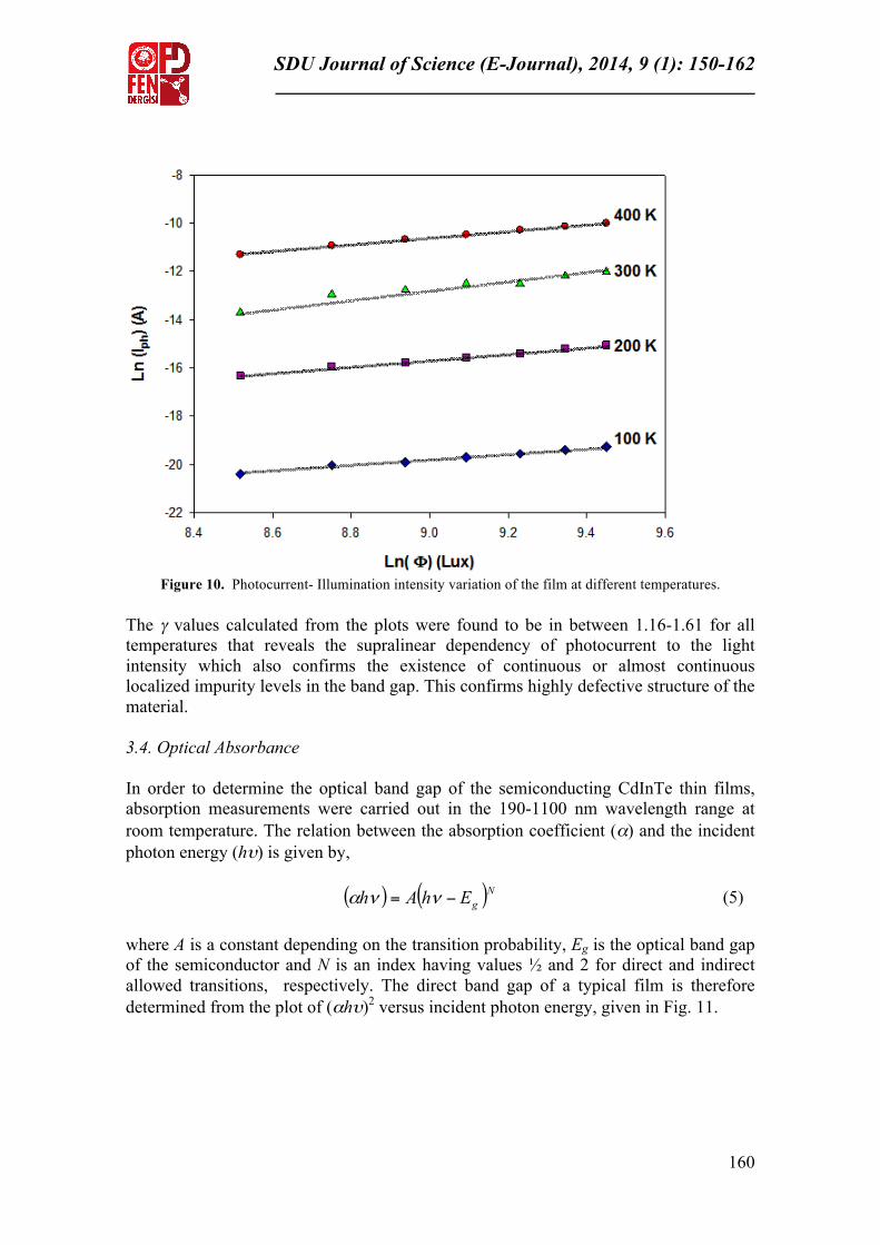
Figure 9. Ln(σ)-1000/T variation at different illumination intensities with an applied electric field of 40 V/cm. The photocurrent was measured along the layer, while the light was incident perpendicular to the layer. As seen from Fig. 9, the conductivity under illumination increases exponentially with increasing temperature for all intensities indicating semiconducting behavior for the film. The photo-thermal activation energies at high temperature region were found to be the same around 250 meV for all intensities which was an indication of a highly degenerate band structure of the film. As the illumination intensity increases, the difference between the photoconductivity values of each intensity decreases due to the ionized impurity levels. Therefore, the photoconductivity is governed by trapping or recombination centers created during the growth of the film. In theory, the characteristics of recombination centers can be found by measuring photocurrent (Iph) versus light intensity (φ) which obeys the relation Iph ∼ φ
γ where the
exponent γ is a function of recombination of the carriers that are not in equilibrium. Ln(Iph)-Ln(φ) variation is shown in Fig.10 at temperatures 100, 200, 300 and 400 K.
SDU Journal of Science (E-Journal), 2014, 9 (1): 150-162 ______________________________________________________
160
Figure 10. Photocurrent- Illumination intensity variation of the film at different temperatures.
The γ values calculated from the plots were found to be in between 1.16-1.61 for all temperatures that reveals the supralinear dependency of photocurrent to the light intensity which also confirms the existence of continuous or almost continuous localized impurity levels in the band gap. This confirms highly defective structure of the material. 3.4. Optical Absorbance In order to determine the optical band gap of the semiconducting CdInTe thin films, absorption measurements were carried out in the 190-1100 nm wavelength range at room temperature. The relation between the absorption coefficient (α) and the incident photon energy (hυ) is given by,
( ) ( )NgEhAh −= ννα (5) where A is a constant depending on the transition probability, Eg is the optical band gap of the semiconductor and N is an index having values ½ and 2 for direct and indirect allowed transitions, respectively. The direct band gap of a typical film is therefore determined from the plot of (αhυ)2 versus incident photon energy, given in Fig. 11.

K. Yılmaz, D. Gölcür
161
Figure 11. Dependence of (αhυ)2 on the incident photon energy for the film. As seen from Fig. 11, the absorption coefficient α decreases exponentially with decreasing photon energy and the absorption coefficient at room temperature was found to be in the order of 104 cm-1. The variation of the optical absorption near the fundamental absorption edge revealed the direct band gap around 1.47 eV for the film with thickness of 0.5 µm. 4. Conclusion Electrical transport, scattering mechanisms, structural and optoelectronic properties of as-grown CdInTe thin films were characterized. We have found that as-grown films were In-rich and Cd-deficient as compared to the stoichiometry of the source powder. The films had polycrystalline nature with hexagonal crystal structure. The dominant conduction mechanism in the temperature range of 200-400 K was found to be thermionic emission of the carriers over the grain boundaries. Conductivity and photo-conductivity analysis revealed an activation energy around 250 meV. Ionized impurity, neutral donor impurity and acoustic phonon scattering mechanisms were effective over three different temperature regions. Absorption coefficient and optical band gap of the films were found to be 104 cm-1 and 1.47 eV, respectively. Thus, it can be concluded from the results of this work that thermally evaporated as-grown CdInTe thin films with n-type conductivity, low resistivity, high absorption coefficient and nearly optimum band gap can be a promising material for possible optoelectronic device applications.
SDU Journal of Science (E-Journal), 2014, 9 (1): 150-162 ______________________________________________________
162
Acknowledgements This work was financially supported by Pamukkale University, Scientific Research Projects Center (BAP), under the project number 2011FBE076. References [1] Lalitha S., Karazhanov S. Zh., Ravindran P., Senthilarasu S., Sathyamoorthy R., Janabergenov J.,
2007. Electronic structure, structural and optical properties of thermally evaporated CdTe thin films, Physica B, 387: 227-238.
[2] Singh S., Kumar R., Sood K. N., 2010. Structural and electrical studies of thermally evaporated nanostructured CdTe thin films, Thin Solid Films, 519: 1078-1081.
[3] Shanmugan S., Mutharasu D., 2010. Effect of Ar+ ion irradiation on structural and optical properties of e-beam evaporated cadmium telluride thin films, Materials Science in Semiconductor Processing, 13: 298-302.
[4] Lalitha S., Sathyamoorthy R., Senthilarasu S., Subbarayan A., Natarajan K., 2004. Characterization of CdTe thin film-dependence of structural and optical properties on temperature and thickness, Solar Energy Materials and Solar Cells, 82: 187-199.
[5] J Fritsche., Kraft D., Thiben A., Mayer T., Klein A., Jaegermann W., 2002. Band energy diagram of CdTe thin film solar cells, Thin Solid Films, 403-404: 252-257.
[6] Bayhan H., Erçelebi Ç., 1998. Effects of post deposition treatments on vacuum evaporated CdTe thin films and CdS/CdTe heterojunction devices, Turkish Journal of Physics, 22: 441-451.
[7] Okamoto T., Yamada A., Konagai M., 2001. Optical and electrical characterizations of highly efficient CdTe thin film solar cells, Thin Solid Films, 387: 6-10.
[8] Dhere N. G., Dhere R. G., 2005. Thin-film photovoltaics, Journal of Vacuum Science and Technology A, 23(4): 1208-1214.
[9] Patil V.B., More P.D., Sutrave D.S., Shahane G.S., Mulik R.N., Deshmukh L.P., 2000. A new process for deposition of the CdTe thin films, Materials Chemistry and Physics, 65: 282-287.
[10] Khairnar U.P., Bhavsar D.S., Vaidya R.U., Bhavsar G.P., 2003. Optical properties of thermally evaporated cadmium telluride thin films, Materials Chemistry and Physics, 80, 421-427.
[11] Iribarren A., Riech I., Hernandez M.P., Castro-Rodriguez R., Pena J. L., Zapata-Torres M., 1999. Optoelectronic properties of polycrystalline CdInTe films, Journal of Vacuum Science and Technology A, 17(6): 3433-3436.
[12] Seto S., Suzuki K., Abastillas V. N. Jr., Inabe K., 2000. Compensating related defects in In-doped bulk CdTe, Journal of Crystal Growth, 214/215: 974-978.
[13] Mohammed W. F., Yousif M. A. S., 2002. The electrical properties of post-deposition annealed and as-deposited In-doped CdTe thin films, Renewable Energy, 26, 285-294.
[14] Zapata-Torres M., Castro-Rodriguez R., Martel A., Mascarenhas Y.P., Guevara J., Melendez-Lira M., Pena J. L., 2001. Structural characterization of polycrystalline Cd–Te–In films, Journal of Vacuum Science and Technology A, 19(1): 246-250.
[15] Fuentes-Cabrera M., Dong J., Sankey O. F., 1999. Theoretical study of the structural, electronic and vibrational properties of CdIn2Te4, Superficies y Vacio, 9: 310-312.
[16] Hong K., 2004. Optical properties of a p-CdIn2Te4 single crystal by the Bridgman method, Journal of the Korean Physical Society, 45: 496-500.
[17] Seto J.Y.W., 1975. The electrical properties of polycrystalline silicon films, Journal of Applied Physics, 46: 5247-5254.
Deniz Gölcür e-mail: [email protected]