invited paper asynchronous techniques for system-on-chip ... · invited paper asynchronous...
TRANSCRIPT

INV ITEDP A P E R
Asynchronous Techniques forSystem-on-Chip DesignDigital circuit designs that are not sensitive to delay promise to allow operation
without clocks for future systems-on-a-chip.
By Alain J. Martin, Member IEEE, and Mika Nystrom, Member IEEE
ABSTRACT | SoC design will require asynchronous techniques
as the large parameter variations across the chip will make it
impossible to control delays in clock networks and other global
signals efficiently. Initially, SoCs will be globally asynchronous
and locally synchronous (GALS). But the complexity of the
numerous asynchronous/synchronous interfaces required in a
GALS will eventually lead to entirely asynchronous solutions.
This paper introduces the main design principles, methods, and
building blocks for asynchronous VLSI systems, with an em-
phasis on communication and synchronization. Asynchronous
circuits with the only delay assumption of isochronic forks are
called quasi-delay-insensitive (QDI). QDI is used in the paper as
the basis for asynchronous logic. The paper discusses asyn-
chronous handshake protocols for communication and the
notion of validity/neutrality tests, and completion tree. Basic
building blocks for sequencing, storage, function evaluation,
and buses are described, and two alternative methods for the
implementation of an arbitrary computation are explained.
Issues of arbitration, and synchronization play an important
role in complex distributed systems and especially in GALS. The
two main asynchronous/synchronous interfaces needed in
GALSVone based on synchronizer, the other on stoppable
clockVare described and analyzed.
KEYWORDS | Arbiter; asynchronous; asynchronous bus;
asynchronous/synchronous interface; C-element; completion
tree; dual-rail; globally asynchronous and locally synchronous
(GALS); half-buffer; handshake protocol; isochronic fork;
metastability; passive–active buffer; precharge half-buffer
(PCHB); quasi-delay-insensitive (QDI); stoppable clock;
synchronizer
I . INTRODUCTION
It is now generally agreed that the sizable very large scale
integration (VLSI) systems [systems-on-chip (SoCs)] of the
nanoscale era will not operate under the control of a singleclock and will require asynchronous techniques. The large
parameter variations across a chip will make it prohibi-
tively expensive to control delays in clocks and other global
signals. Also, issues of modularity and energy consumption
plead in favor of asynchronous solutions at the system
level. Whether those future systems will be entirely asyn-
chronous, as we predict, or globally asynchronous and
locally synchronous (GALS), as more conservative practi-tioners would have it, we anticipate that the use of asyn-
chronous methods will be extensive and limited only by
the traditional designers’ relative lack of familiarity with
the approach. Fortunately, the past two decades have
witnessed spectacular progress in developing methods and
prototypes for asynchronous (clockless) VLSI. Today, a
complete catalogue of mature techniques and standard
components, as well as some computer-aided design (CAD)tools, are available for the design of complex asynchro-
nous digital systems.
This paper introduces the main design principles,
methods, and building blocks for asynchronous VLSI
systems, with an emphasis on communication and synchro-
nization. Such systems will be organized as distributed
systems on a chip consisting of a large collection of com-
ponents communicating by message exchange. Therefore,the paper places a strong emphasis on issues related to
network and communicationVissues for which asynchro-
nous techniques are particularly well-suited. Our hope is
that after reading this paper, the designer of an SoC should
be familiar enough with those techniques that he or she
would no longer hesitate to use them. Even those adepts of
GALS who are adamant not to let asynchrony penetrate
further than the network part of their SoC must realize thatnetwork architectures for SoCs are rapidly becoming so
complex as to require the mobilization of the complete
armory of asynchronous techniques.
Manuscript received September 14, 2005; revised March 3, 2006. This work was
supported in part by the Defense Advanced Research Projects Agency (DARPA).
The authors are with the Department of Computer Science, California Institute of
Technology, Pasadena, CA 91125 USA (e-mail: [email protected]).
Digital Object Identifier: 10.1109/JPROC.2006.875789
Vol. 94, No. 6, June 2006 | Proceedings of the IEEE 10890018-9219/$20.00 �2006 IEEE
The paper is organized as follows. The second sectioncontains a brief history and the main definitions of the
different asynchronous logics according to their timing
assumptions. Section III introduces the computational
models and languages used in this paper to describe and
construct asynchronous circuits. Section IV introduces the
most common asynchronous communication protocols and
the notion of validity/neutrality tests. Basic building blocks
for sequencing, storage, and function evaluation are intro-duced in Section V. Section VI presents two alternative
methods for the implementation of an arbitrary computa-
tion: syntax-directed decomposition and data-driven decom-
position. The two approaches differ in how a specification is
decomposed into pipeline stages. Section VII describes
several implementations of buses. Section VIII deals with
issues of arbitration, and synchronization. Section IX pre-
sents the asynchronous/synchronous interfaces needed in aGALS system.
II . A BRIEF HISTORY AND AFEW DEFINITIONS
The field of asynchronous design is both old and new. The
1952 ILLIAC and the 1962 ILLIAC II at the University of
Illinois are said to have contained both synchro-nous and asynchronous parts [2]. The 1960 PDP6
from Digital Equipment (DEC) was also asyn-
chronous [52]. The Bmacromodule[ experiment
in the 1960s proposed asynchronous building
blocks that, in spirit, are very close to a modern
system-level approach [10] and to GALS. Impor-
tant theoretical contributions of this period
include the works of Huffman [20], Muller [33],and Unger [53]. An excellent presentation of
Muller’s work is in [32]. The pioneering work of Molnar
and his colleagues at Washington University was instru-
mental in explaining metastability [6].
Even though asynchronous logic never disappeared
completely, when clocked techniques offered an easy way
of dealing with timing and hiding hazards, clockless logic
was all but forgotten until the arrival of VLSI in the late1970s. The first Caltech Conference on VLSI in 1979 con-
tained a complete session on Bself-timed[ logic, as asyn-
chronous logic was called at the time, with in particular an
important paper by Stucki and Cox on Bsynchronization
strategies[ presenting the first pausable clockVas we shall
see, an important device in GALSVand discussing meta-
stability [47]. Seitz’s chapter on system timing in Mead and
Conway’s epoch-making 1980 Introduction to VLSI Systemsrevived the research community’s interest in the topicVif
not the industry’s interest [31], [45].
The first Bmodern[ synthesis methods appear around
the mid1980 with the Caltech program-transformation
approach [24] and T.-A. Chu’s State-transition-graph (STG)
approach [8]. Soon after, Burns and Martin, Brunvand,
and van Berkel proposed similar methods for the syntax-
directed compilation of high-level description into asyn-chronous circuits [3], [5]. Petrify is a more recent tool for
the synthesis of asynchronous controllers described as
Petri nets [12].
The first single-chip asynchronous microprocessor was
designed at Caltech in 1988 [27]. It was followed by the
first BAmulet[ (a family of asynchronous clones of the
ARM processor) from the University of Manchester in
1993 [14], the TITAC, an 8-bit microprocessor from theTokyo Institute of Technology in 1994 [36], and the
Amulet2e and TITAC-2 in 1997 [15], [37]Vthe TITAC-2 is
a 32-bit microprocessor. Also in 1997, the Caltech group
designed the MiniMIPS, an asynchronous version of the
32-bit MIPS R3000 microprocessor [28]. With a perfor-
mance close to four times that of a clocked version in the
same technology for the first prototype, the MiniMIPS is,
at the moment of writing, still the fastest complete asyn-chronous processor ever fabricated [30]. A group at
Grenoble ported the Caltech MiniMIPS building blocks
to standard cells to use in a 16-bit RISC [42]. Other asyn-
chronous chip experiments include the design of a fast
divider at Stanford in 1991 [49], and an instruction-length
decoder for the Pentium by a research group at Intel in 1999
[44]. Low-power asynchronous microcontrollers have been
designed at Philips [17], Caltech [30], and Cornell [21].
The concept of GALS was first proposed by Chapiro [7] in
1984. It has recently gained in popularity, in particular
with the work of a group at Zurich [35].
Several books on asynchronous logic have been
published. Among them, our favorites are [11], [34], and
[46]. A special issue of the Proceedings of the IEEE also givesa good overview of the state of the art [38]. The book by
Dally and Poulton, although not specifically about asyn-
chronous systems contains an excellent chapter on syn-
chronization [13]. The on-line Asynchronous Bibliographymaintains an updated bibliography of the field to date [1].
A digital circuit is asynchronous when no clock is used
to implement sequencing. Such circuits are also called
clockless. The various asynchronous approaches differ intheir use of delay assumptions to implement sequencing. Acircuit is delay-insensitive (DI) when its correct operation isindependent of any assumption on delays in operators andwires except that the delays are finite and positive. The term
delay-insensitive appears informally in [45]. It was proved
in 1990 that in a model in which all delays are exposedVthe building blocks are elementary gates with a single
A digital circuit is asynchronouswhennoclock is used to implementsequencing. Such circuits are alsocalled clockless.
Martin and Nystrom: Asynchronous Techniques for System-on-Chip Design
1090 Proceedings of the IEEE | Vol. 94, No. 6, June 2006

Boolean outputVthe class of entirely delay-insensitivecircuits is very limited [26]. Most circuits of interest to the
digital designer fall outside the class. But it can also be
proved that a single delay assumption on certain forks
connecting the output of a gate to the inputs of several
other gates is enough to implement a Turing machine, and
therefore the whole class of Turing-computable functions
[23]. Those forks are called isochronic.
Asynchronous circuits with the only delay assumption ofisochronic forks are called quasi-delay-insensitive (QDI).
We use QDI as the basis for asynchronous logic. All other
forms of the technology can be viewed as a transformation
from a QDI approach by adding some delay assumption. An
asynchronous circuit in which all forks are assumed
isochronic corresponds to what has been called a speed-independent circuit, which is a circuit in which the delays in
the interconnects (wires and forks) are negligible com-pared to the delays in the gates. The concept of speed-
independent circuit was introduced by Muller [33].
Similarly, self-timed circuits are asynchronous circuits in
which all forks that fit inside a chosen physical area called
equipotential region are isochronic [45].
Several styles of asynchronous circuits currently in use
fall into some hybrid category. They rely on some specific
timing assumption besides the implicit QDI assumption.For instance, the Bbundled data[ technique uses a timing
assumption to implement the communication protocol
between components. Another approachVtimed asynchro-nous logicVstarts from a QDI circuit, and then derives
timing relations between events in the QDI computation
that are used to simplify the solution. (See [34].) Yet
another approach uses a timing assumption to control the
reset phase of the handshake protocol (to be explainedlater). Two logic families based on this approach are
asynchronous pulse logic ([40]) and GasP ([48]).
III . SOC S AS DISTRIBUTED SYSTEMS
SoCs are complex distributed systems in which a large
number of parallel components communicate with one
another and synchronize their activities by message ex-change. At the heart of digital logic synthesis lie funda-
mental concurrency issues like concurrent read and write
of variables and synchronization between send and receive
commands. Synchronous (clocked) logic brings a simple
solution to the problem by partially ordering transitions
with respect to a succession of global events (clock signals)
so as to order conflicting read/write actions. In the absence
of a global time reference, asynchronous logic has to dealwith concurrency in all its generality, and asynchronous-
logic synthesis relies on the methods and notations of
concurrent computing. There exist many languages for
distributed computing. The high-level language used in
this paper is called Communicating Hardware Processes(CHP). It is based on CSP [19], and is used widely in one
form or other in the design of asynchronous systems.
We introduce only those constructs of the language neededfor describing the method and the examples, and that are
common to most computational models based on commu-
nication. The systematic design of an SoC is a process of
successive refinements taking the design from a high-
level description to a transistor netlist. The three levels of
representationVCHP, HSE, PRSVused in this paper
mirror the three main stages of the refinement.
A. Modeling Systems: Communicating ProcessesA system is composed of concurrent modules called
processes. Processes do not share variables but communi-
cate only by send and receive actions on ports.
1) Communication, Ports, and Channels: A send port of a
processVsay, port R of process p1Vis connected to a
receive port of another processVsay, port L of processp2Vto form a channel. A receive command on port L is
denoted L?y. It assigns to local variable y the value received
on L. A send command on port R, denoted R!x, assigns to
port R the value of local variable x. The data item
transferred during a communication is called a message.
The net effect of the combined send R!x and receive L?yis the assignment y :¼ x together with the synchronization
of the send and receive actions.The slack of a channel is the maximal difference
between the number of completed send actions and the
number of completed receive actions on the two ports of
the channel. In other words, the slack is the capacity of the
channel to store messages. Since we implement channels
with wires only, we choose to have slack-zero channels: the
completion of a send at one end of the channel coincides
with the completion of a receive at the other end of thechannel. Both send and receive actions are said to be
Bblocking.[ A send or receive action on a port may have to
be delayed (pending) until the matching action on the
other port of the channel is ready.
2) Assignment: The value of a variable is changed by an
explicit assignment to the variable as in x :¼ expr. For bBoolean, b " and b # stand for b :¼ true and b :¼ false,respectively.
3) Sequential and Parallel Compositions: CHP and HSE
provide two composition operators: the sequential oper-
ator S1; S2 and the parallel operator. Unrestricted use of
parallel composition would cause read/write conflicts on
shared variables. CHP restricts the use of concurrency in
two ways. The parallel bar k, as in S1kS2, denotes theparallel composition of processes.1 CHP also allows a
limited form of concurrency inside a process, denoted by
the comma, as in S1, S2. The comma is restricted to
1In CHP, processes do not share variables. In HSE, the only sharedvariables are those introduced for the implementation of communication.They cannot cause read/write conflicts.
Martin and Nystrom: Asynchronous Techniques for System-on-Chip Design
Vol. 94, No. 6, June 2006 | Proceedings of the IEEE 1091

program parts that are noninterfering: if S1 writes x, then S2neither reads x nor writes x.
4) Selection, Wait, and Repetition: The selection command½B1 ! S1½�B2 ! S2½� . . .� is a generalization of the if-
statement. It has an arbitrary number (at least one) of
clauses, called Bguarded commands,[ Bi ! Si where Bi is a
Boolean condition and Si is a program part. The execution
of the selection consists of: 1) evaluating all guards and2) executing the command Si with the true guard Bi. In
this version of the selection, at most one guard can be
true at any time. There is also an arbitrated version
where several guards can be true. In that case, an
arbitrary true guard is selected. The arbitrated selection
is identified by a thin bar as in ½B1 ! S1jB2 ! S2�.In both versions, when no guard is true, the execution is
suspended: the execution of the selection reduces to a waitfor a guard to become true. Hence, waiting for a condition to
be true can be implemented with the selection ½B ! skip�,where skip is the command that does nothing but ter-
minates. A shorthand notation for this selection is ½B�.In this paper, we use only the nonterminating
repetition ½S� that repeats S forever.
5) Pipeline Slack and Slack Matching: Slack matching isan optimization by which simple buffers are added to a
system of distributed processes to increase the throughput.
A pipeline is a connected subgraph of the process graph
with one input port and one output port. The static slack of
a pipeline is the maximal number of messages the pipeline
can hold. A pipeline consisting of chain of n simple buff-
ers has a static slack of n, since each simple buffer can
hold at most one message, and the channels have slackzeroVunless, as we shall see, the buffers implementa-
tions are subjected to a transformation called reshuffling,
which can reduce their slack.
The dynamic slack of a pipeline denotes the number of
messages or, more generally, the range of numbers of
messages that the pipeline must hold to run at optimal
throughput. For the same pipeline of n simple buffers with
a symmetric implementation, the dynamic slack is cen-tered around n=2. (See [22], [41].) However, the most
efficient buffer templates are not symmetricalVthey favor
forward latency over backward latency. For such buffers,
the dynamic-slack range is reduced, typically centering
around n=8 for the MiniMIPS. (The definitions of static
and dynamic slacks are easy to extend to rings of processes.)
B. Modeling System Components: HSEEach CHP process is refined into a partial order of
signal transitions, i.e., transitions on Boolean variables.
The HSE notation is not different from CHP except that it
allows only Boolean variables, and send and receive
communications have been replaced with their handshak-ing expansion in terms of the Boolean variables modeling
the communication wires. The modeling of wires intro-
duces a restricted form of shared variables between
processes (the variables implementing channels). A typical
example of an HSE program is
½li�; ro "; ½ri�; ro #; ½:ri�; lo "; ½:li�; lo #½ �:
The input variables li and ri can only be read. The output
variables lo and ro can be read and written. The above
example can be read as follows. BRepeat forever: wait for
li to be true; set ro to true; wait for ri to be true; set ro to
false; etc . . .[
C. Modeling Circuits: Production RulesA circuitVfor instance, a CMOS circuitVis a network
of operators (logic gates). Each gate has an arbitrary
number of inputs (in practice this number is limited by the
resistance of transistor chains), and one output. (The only
exceptions are arbiter and synchronizer, which each have
two inputs and two outputs.) A logic gate with Boolean
output z sets z to true when a Boolean condition Bu of itsinputs holds, and sets z to false when a Boolean condition
Bd of its inputs holds. Those behaviors are formalized by
the two production rules
Bu ! z "Bd ! z # :
A production rule (PR) is a construct of the form B ! t where tis a simple assignment (a transition) and B is a Booleanexpression called the guard of the PR. A production rule set(PRS) is the parallel composition of all production rules in theset. Each pair of complementary PRs,Vthe production
rules that set and reset the same variableVis identified and
implemented with (standard or nonstandard) CMOS
operators. In order to carry over the robustness and delayinsensitivity of the design to the circuit level, all operators
are restoring (they have gain) and static (the output node is
never Bfloating[).
Fig. 1. The pull-up and pull-down networks implementing a CMOS logic
gate. (a) Combinational gate. (b) State-holding gate with a standard
Bstaticizer[ (Bkeeper[). The circled transistors are weak.
Martin and Nystrom: Asynchronous Techniques for System-on-Chip Design
1092 Proceedings of the IEEE | Vol. 94, No. 6, June 2006
Complementary PRs must be noninterfering, i.e., guards
Bu and Bd cannot be true at the same time. If Bu ¼ :Bd,
then either Bu or Bd holds at any time, and output z is
always connected to either the Vdd or the groundVz is
always Bdriven.[ In this case, the operator is combinationalwith the simple CMOS implementation of Fig. 1(a). Ifthere are states in the computation where neither Bu nor
Bd holds, then output z is Bfloating[ in those states. The
operator has to maintain the current value of z and is
therefore state-holding. In a QDI circuit, a state-holding
operator is usually implemented with the Bkeeper[ or
Bstaticizer[ shown in Fig. 1(b). (Adding a staticizer in-
troduces interferences between the original PRs and the
rules added by the feedback inverter. The interferences areresolved by making the transistors of the feedback inverter
Bweak,[ i.e., with low drain-to-source current.) Alterna-
tively, the state-holding operator can be transformed into a
combinational one, like the nor-gate implementation of
the set–reset shown in Fig. 2(b).
1) Combinational Gates: With the exception of the
Bwrite-acknowledge,[ we use standard combinationalgates in this paper: inverter, nand, nor. nand- and nor-
gates may have multiple inputs. Because of the restriction
on the length of transistor chains, a multiple-input gate
may have to be decomposed into a tree of smaller gates.2
2) State-Holding Elements: The three state-holding gates
used in this paper are the Muller C-element, the set–reset
gate, and the precharge function. The Muller C-element(also called C-element) with inputs x and y and output z,
denoted z ¼ x C y, implements the PRs x ^ y ! z " and
:x ^ :y ! z #. The C-element is a state-holding element,
since the current value of z must be maintained when
x 6¼ y. The three-input C-element (denoted 3C) is used in a
few examples in the paper. The set–reset gate with inputs sand r and output z has the PRs s ! z " and r ! z #.
Since s and r must be mutually exclusive, it is alwayspossible to implement the set–reset gate as the C-elementz ¼ sC:r. This implementation requires to invert either sor r. Rather, we can code z with the two variables zt and zf ,such that zt ¼ :zf , and we implement the set–reset gateeither with two cross-coupled nor-gates or two cross-coupled inverters as shown in Fig. 2(b) and (c).
We also use a nonstandard operator, the prechargefunction (PCF). An example of a precharge function withinputs en, x:0, x:1, y:0, y:1 and output z is described by thefollowing two PR pairs:
en ^ ðx:0 ^ y:0 _ x:1 ^ y:1Þ ! z:1 #:en ! z:1 "
en ^ ðx:0 ^ y:1 _ x:1 ^ y:0Þ ! z:0 #:en ! z:0 " :
This gate computes the function X ¼ Y where X, Y, and Zare dual-rail encoded; en is a control signal. This gate is alsoa state-holding element. The PCF can be used for anyfunction (Boolean or 1-of-N) whose CMOS pulldown-networks do not exceed the limit on transistor-chain length.
D. Stability and NoninterferenceStability and noninterference are the two properties of
PRS that guarantee that the circuits are operating cor-rectly, i.e., without logic hazards. A hazard is the possibilityof an incomplete transition (a Bglitch[).3
2Large-gate decomposition is an annoying problem in asynchronousdesign, since it may violate stability. The decomposition of a multi-inputor-gate we use in the paper is stable because a transition on the output iscaused by exactly one input transition.
Fig. 2. State-holding elements. (a) The C-element. (b) NOR-gate implementation of set–reset. (c) Inverter implementation of set–reset. (d) Example
of a precharge function. The cross-coupled inverters in (a) and (b) are standards Bstaticizers.[ The letter w indicates that the transistors of
the inverter are weak.
3Of course, electrical effects, in particular charge sharing and cross-talk, can also produce voltage glitches that are not eliminated by stabilityand noninterference.
Martin and Nystrom: Asynchronous Techniques for System-on-Chip Design
Vol. 94, No. 6, June 2006 | Proceedings of the IEEE 1093

How do we guarantee the proper execution of pro-duction rule G ! t? In other words, what can go wrong
and how do we avoid it? Two types of malfunction may
take place: 1) G may cease to hold before transition t has
completed, as the result of a concurrent transition
invalidating G, and 2) the complementary transition t0 of tis executed while the execution of t is in progress, leading
to an undefined state. We introduce two requirements,
stability and noninterference that eliminate the two sourcesof malfunction.
The Bresult[ RðtÞ of a transition t is defined as
Rðx "Þ ¼ x, and Rðx #Þ ¼ :x, for any x.
Definition 1: A production rule G ! t is said to be stable
in a computation if and only if G can change from true to
false only in those states of the computation in which RðtÞholds. A production-rule set is said to be stable if and onlyif all production rules in the set are stable.
Definition 2: Two production rules Bu ! x " and
Bd ! x # are said to be noninterfering in a computation
if and only if :Bu _ :Bd is an invariant of the computation.
A production-rule set is noninterfering if every pair of com-
plementary production rules in the set is noninterfering.
Any concurrent execution of a stable and noninterfer-ing PRS is equivalent to the sequential execution model in
which, at each step of the computation, a PR with a true
guard is selected and executed. The selection of the PR
should be weakly fair, i.e., any enabled PR is eventually
selected for execution.
The existence of a sequential execution model for QDI
computations greatly simplifies reasoning about, and
simulating, those computations. Properties similar tostability are used in other theories of asynchronous
computations, in particular, semimodularity [33] and
persistency [11]. Consider rule B ^ x ! x # as part of a
gate G with output x. At the logical level, the execution
of transition x # when the guard holds invalidates the
guard. (Such production rules are therefore called self-invalidating.) We exclude self-invalidating production rules,since, in most implementations, they would violate the sta-bility condition.
E. Isochronic ForksA computation implements a partial order of transi-
tions. In the absence of timing assumptions, this partial
order is based on a causality relation. For example,
transition x " causes transition y # in state S if and only if
x " makes guard By of y # true in S. Transition y # is said toacknowledge transition x ". We do not have to be more
specific about the precise ordering in time of transitions
x " and y #. The acknowledgment relation is enough to
introduce the desired partial order among transitions, and
to conclude that x " precedes y #. In an implementation of
the circuit, gate Gx with output x is directly connected to
gate Gy with output y, i.e., x is an input of Gy.
Hence, a necessary condition for an asynchronous circuitto be delay-insensitive is that all transitions are acknowledged.
Unfortunately, the class of computations in which all
transitions are acknowledged is very limited. Consider the
example of Fig. 3. Signal x is forked to x1, an input of gate
Gy with output y, and to x2, an input of gate Gz with
output z. A transition x " when c holds is followed by a
transition y ", but not by a transition z ", i.e., transitionx1 " is acknowledged but transition x2 " is not, and viceversa when :c holds. Hence, in either case, a transition on
one output of the fork is not acknowledged. In order to
guarantee that the unacknowledged transition completes
without violating the specified order, a timing assumption
called the isochronicity assumption has to be introduced,
and the forks that require that assumption are called
isochronic forks [26]. (Not all forks in a QDI circuit areisochronic.) Most circuits presented in this paper contain
isochronic forks. A typical instance is the fork with input qiin Fig. 13 describing a single-bit register.
The timing assumption on isochronic forks is a one-
sided inequality that can always be satisfied: it requires
that the delay of a single transition be shorter that the
sum of the delays on a multitransition path. It can be
proved by constructing a Turing machine as a QDI circuit(see [23]) that the class of QDI circuits is Turing-
complete, i.e., all Turing-computable functions have a
QDI implementation.
IV. ASYNCHRONOUS COMMUNICATIONPROTOCOLS
The implementation of send/receive communication iscentral to the methods of asynchronous logic, since this
form of communication is used at all levels of system de-
sign, from communication between, say, a processor and a
cache down to the interaction between the control part
and the datapath of an ALU. Communication across a
channel connecting two asynchronous components p1 and
Fig. 3. The fork (x, x1, x2) is isochronic: a transition on x1 causes a
transition on y only when c is true, and a transition on x2 causes a
transition on z only when c is false. Hence, certain transitions on x1
and on x2 are not acknowledged, and therefore a timing assumption
must be used to guarantee the proper completion of those
unacknowledged transitions.
Martin and Nystrom: Asynchronous Techniques for System-on-Chip Design
1094 Proceedings of the IEEE | Vol. 94, No. 6, June 2006

p2 is implemented as a handshake protocol. In a later sec-tion, we will describe how to implement communication
between a synchronous (clocked) component and an asyn-
chronous one. Such interfaces are needed in a GALS SoC.
A. Bare Handshake ProtocolLet us first implement a Bbare[ communication be-
tween processes p1 and p2: no data is transmitted. (Bare
communications are used as a synchronization point be-tween two processes.) In that case, channel ðR; LÞ can be
implemented with two wires: wire ðro; liÞ and wire ðlo; riÞ.(The wires that implement a channel are also called rails.)
See Fig. 4.
Wire ðro; liÞ is written by p1 and read by p2. Wire ðlo; riÞis written by p2 and read by p1. An assignment ro " or ro #in p1 is eventually followed by the corresponding
assignment li " or li # in p2 due to the behavior of wireðro; liÞ. And symmetrically for variables lo and ri, and wire
ðlo; riÞ. By convention, and unless specified otherwise, all
variables are initialized to false.
1) Two-Phase Handshake: The simplest handshake
protocol implementing the slack-zero communication
between R and L is the so-called two-phase handshakeprotocol, also called nonreturn to zero (NRZ). The protocolis defined by the following handshake sequence Ru for Rand Lu for L:
Ru : ro "; ½ri�Lu : ½li�; lo " :
Given the behavior of the two wires ðro; liÞ and ðlo; riÞ, the
only possible interleaving of the elementary transitions of
Ru and Lu is ro "; li "; lo "; ri ".
This interleaving is a valid implementation of a slack-
zero execution of R and L, since there is no state in the
system where one handshake has terminated and the other
has not started. But now all handshake variables are true,
and therefore the next handshake protocol for R and Lhas to be
Rd : ro #; ½:ri�Ld : ½:li�; lo # :
The use of the two different protocols is possible if it can be
statically determined (i.e., by inspection of the CHP code)
which are the even (up-going) and odd (down-going)phases of the communication sequence on each channel.
But if, for instance, the CHP program contains a selection
command, it may be impossible to determine whether a
given communication is an even or odd one. In that case, a
general protocol has to be used that is valid for both phases,
as follows:
R : ro :¼ :ro; ½ro ¼ ri�L : ½lo 6¼ li�; lo :¼ :lo :
This protocol has a complicated circuit implementation,
requiring exclusive-or gates and the storage of the current
values of lo and ro. Two-phase handshake also requires that
arithmetic and logical operations performed on the data
transmitted be implemented in both upgoing and down-going logics, which is quite inefficient. Therefore, in spite
of its simplicity, the two-phase handshake protocol is rarely
used besides some obvious cases.
2) Four-Phase Handshake: A straightforward solution is
to always reset all variables to their initial value (zero).
Such a protocol is called four-phase or return-to-zero (RZ).
R is implemented as Ru; Rd and L as Lu; Ld as follows:
R : ro "; ½ri�; ro #; ½:ri�L : ½li�; lo "; ½:li�; lo # :
In this case, the only possible interleaving of transitions for
a concurrent execution of R and L is ro "; li "; lo "; ri ";ro #; li #; lo #; ri #.
Again, it can be shown that this interleaving imple-
ments a slack-zero communication between R and L. It can
even be argued that this implementation is in fact the
sequencing of two slack-zero communications: the first
one between Ru and Lu, the second one between Rd andLd. This observation will be used later to optimize the
protocols by a transformation called reshuffling.
B. Handshake Protocols With Data: Bundled DataLet us now deal with the case when the communi-
cation also entails transmitting data, for instance, by
sending on RðR!xÞ and receiving on LðL?yÞ. A solutionimmediately comes to mind: let us add a collection of
data wires next to the handshake wires. The data wire
ðrd; ldÞ is indicated by a double arrow on Fig. 5. The
protocols are as follows:
R!x : rd :¼ x; ro "; ½ri�; ro #; ½:ri�L?y : ½li�; y :¼ ld; lo "; ½:li�; lo # :
This protocol relies on the timing assumption that the order
between rd :¼ x and ro " in the sender is maintained in the
Fig. 4. Implementation of a Bbare[ channel (L;R) with two handshake
wires: (lo; ri) and (ro; li).
Martin and Nystrom: Asynchronous Techniques for System-on-Chip Design
Vol. 94, No. 6, June 2006 | Proceedings of the IEEE 1095

receiver: when the receiver has observed li to be true, it can
assume that ld has been set to the right value, which
amounts to assuming that the delay on wire ðro; liÞ is always
Bsafely[ longer than the delay on wire ðrd; ldÞ. Such a
protocol is used and is called bundled-data. The efficiency of
bundle-data versus DI codes is a hotly debated issue. Wewill discuss it later.
C. DI Data CodesIn the absence of timing assumptions, the protocol
cannot rely on a single wire to indicate when the data wireshave been assigned a valid value by the sender. The validity
of the data has to be encoded with the data itself. A DI data
code is one in which the validity and neutrality of the data
are encoded within the data. Furthermore, the code is
chosen such that when the data changes from neutral to
valid, no intermediate value is valid; when the data
changes from valid to neutral, no intermediate value is
neutral. Such codes are also called separable. There aremany DI codes but two are almost exclusively used on
chipVthe dual-rail and 1-of-N codes.
D. Dual-Rail CodeIn a dual-rail code, two wires, bit.0 and bit.1, are used
for each bit of the binary representation of the data. [See
Fig. 6(a).] The neutral and valid values are encoded as
follows:
value : neutral 0 1
bit:0 : 0 1 0bit:1 : 0 0 1
For a two-bit data word ðx0; x1Þ, its dual-rail encoding is
value : neutral 0 1 2 3
x0:0 : 0 1 0 1 0
x0:1 : 0 0 1 0 1
x1:0 : 0 1 1 0 0
x1:1 : 0 0 0 1 1
E. 1-of-N CodesIn a 1-of-N code, one wire is used for each value of the
data. Hence, the same two-bit data word is now encoded as
follows:
value : neutral 0 1 2 3d:0 : 0 1 0 0 0
d:1 : 0 0 1 0 0
d:2 : 0 0 0 1 0
d:3 : 0 0 0 0 1
For a Boolean data-word, dual-rail and 1-of-N are obviously
identical. For a 2-bit data word, both dual-rail and 1-of-4
codes require four wires. For an N-bit data word, dual-rail
requires 2 N wires. If the bits of the original word arepaired and each pair is 1-of-4 encoded, this coding also
requires 2 N wires. An assignment of a valid value to a
dual-rail-coded word requires 2 N transitions, but
requires only N transitions in the case of a 1-of-4 code.
[See Fig. 6(b).]
F. k-out-of-N CodesThe 1-of-N code, also called one-hot, is a special case of
a larger class of codes called k-out-of-N. Instead of using
just one true bit out of N code bits, as is done in the 1-of-N,
we may use k, 0 G k G N, true bits to represent a valid code
value. The number of valid values of a k-out-of-N code isNk
� �. Hence, the maximal number of valid values for a given
N is obtained by choosing k as N=2. Sperner has proved
that this code is not only the optimal k-out-of-N code, but
also the optimal DI code in terms of the size of the code set
for a given N.
G. Which DI Code?The choice of a DI code in the design of a system on a
chip is dictated by a number of practical requirements.
First, the tests for validity and neutrality must be simple.
The neutrality test is simple: as in all codes, the unique
neutral value is the set of all zeroes or the set of all ones.But the validity test may vary greatly with the code.
Second, the coding and decoding of a data word must be
simple. Third, the overhead in terms of the number of bits
used for a code word compared to the number of bits used
for a data word should be kept reasonably small. Finally,
the code should be easy to Bsplit[: a coded word is often
split into portions that are distributed among a number of
processesVfor example, a processor instruction may bedecomposed into an opcode, and several register fields. It
is very convenient if the portions of a code word are
themselves a valid code word. This is the case for the dual-
rail code for all partitions and for the 1-of-4 code for
partitions down to a quarter-byte. For all those practical
reasons, dual-rail and 1-of-4 are used almost exclusively in
asynchronous VLSI design.
Fig. 5. A bundled-data communication protocol. The cigar shape on the
control wire (ro; li) indicates that the delay �� on the wire has been
adjusted to be longer than the delays on the data wires (rd; ld).
Martin and Nystrom: Asynchronous Techniques for System-on-Chip Design
1096 Proceedings of the IEEE | Vol. 94, No. 6, June 2006
H. Validity and Neutrality TestsThe combination of four-phase handshake protocol and
DI code for the data gives the following general
implementation for communication on a channel. In thisgeneric description, we use global names for both the
sender and receiver variables. A collection of data wires
called data encodes the message being sent. A single
acknowledge wire ack is used by the receiver to notify the
sender that the message has been received. This wire is
called the enable wire when it is initialized high (true).
The data wires are initially set to the neutral value of
the code. The concurrent assignment denoted data * takesthe data wires from the neutral value to a valid value. The
concurrent assignment data + takes the data wires from a
valid value back to the neutral value. The protocols for
sender and receiver can be described as
Send : data *; vðackÞ½ �; data +; nðackÞ½ �Receive : vðdataÞ½ �; ack "; nðdataÞ½ �; ack # :
The predicate vðXÞ, called validity test, is used to
determine that X is a valid value for the chosen DI code.The predicate nðXÞ, called neutrality test, is used to
determine that x has the neutral value in the chosen DI
code. The implementations of validity and neutrality tests
play an important role in the efficiency of QDI systems.
1) Active and Passive Protocols: There is an asymmetry in
the (two-phase and four-phase) handshake protocols
described in the previous section: one side, here thesender, starts by setting some output variables (wires) to a
valid value. Such a protocol is called active. The other side,
here the receiver, starts by waiting for some input variables
(wires) to have a valid value. Such a protocol is called
passive. Symmetrical protocols are possible but are more
complicated and therefore rarely used.
Of course, an active protocol on one side of a channel
has to be matched to a passive protocol on the other side ofthe same channel. It seems Bnatural[ to choose the sender
side to be active and the receiver side to be passive, but in
fact, the sender can be passive and the receiver active. We
will see cases when this is a better choice. The protocol is
then as follows:
Send : vðackÞ½ �; data *; nðackÞ½ �; data +Receive : ack "; vðdataÞ½ �; ack #; nðdataÞ½ �:
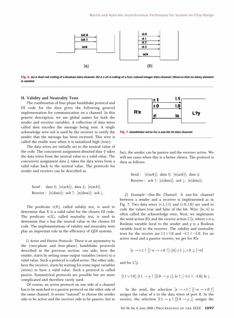
2) ExampleVOne-Bit Channel: A one-bit channel
between a sender and a receiver is implemented as in
Fig. 7. Two data wires ðr:1; l:1Þ and ðr:0; l:0Þ are used tocode the values true and false of the bit. Wire ðlo; riÞ is
often called the acknowledge wire. Next, we implement
the send action R!x and the receive action L?y, where x is a
Boolean variable local to the sender and y is a Boolean
variable local to the receiver. The validity and neutrality
tests for the receive are l:1 _ l:0 and :l:1 ^ :l:0. For an
active send and a passive receive, we get for R!x
½x ! r:1 " ½�:x ! r:0 "�; ½ri�; r:1 #; r:0 #; ½:ri�
and for L?y
½l:1 _ l:0�; ½l:1 ! y " ½�l:0 ! y #�; lo "; ½:l:1 ^ :l:0�; lo # :
In the send, the selection ½x ! r:1 " ½�:x ! r:0 "�assigns the value of x to the data wires of port R. In thereceive, the selection ½l:1 ! y " ½�l:0 ! y #� assigns the
Fig. 7. Handshake wires for a one-bit DI data channel.
Fig. 6. (a) A dual-rail coding of a Boolean data-channel. (b) A 1-of-4 coding of a four-valued integer data channel. Observe that no delay element
is needed.
Martin and Nystrom: Asynchronous Techniques for System-on-Chip Design
Vol. 94, No. 6, June 2006 | Proceedings of the IEEE 1097

value of the data wires of port L to y. In practice, the
internal variables x and y are also dual-rail encoded. In
the receive, the validity test ½l:1 _ l:0� is superfluous, since
the selection following it also includes waiting for l:1 or
l:0. We can rewrite the HSE of the receive L?y as
½l:1�!y " ½�l:0 ! y #�; lo "; ½:l:1 ^ :l:0�; lo # :
For passive send and active receive, the solution for R!x is
½ri�; ½x�!r:1 " ½�:x ! r:0 "�; ½:ri�; r:1 #; r:0 #
and for L?y
lo "; ½l:1�!y " ½�l:0�!y #�; lo #; ½:l:1 ^ :l:0�:
V. BASIC BUILDING BLOCKS:SEQUENCING, STORAGE,COMPUTATION
The three basic building blocks are: 1) a circuit that
sequences two bare communication actionsVthe sequenc-
ing of any two arbitrary actions can be reduced to the
sequencing of two bare communications; 2) a circuit that
reads and writes a single-bit register; and 3) a circuit that
computes a Boolean function of a small number of bits.
A. SequencerThe basic sequencing building block is the Bsequencer[
process, also called Bleft–right buffer[ p1 : ½L; R� which
repeatedly does a bare communication on its left port Lfollowed by a bare communication on its right port R. Thetwo ports are connected to an environment which imposes
no restriction on the two communications. The simplest
implementation is when both ports are active. (The reason
is that a handshake on a passive port is initiated by the
environment and therefore requires extra effort to besynchronized.) For L and R (bare) active ports, the HSE
of p1 is
lo "; ½li�; lo #; ½:li�; ro "; ½ri�; ro #; ½:ri�½ �:
The state preceding ro " and the state preceding lo " are
identical in terms of the variables of the HSE, and thereforethe states in which each of the two transitions is to fire
cannot be separated. We introduce a state variable x(initially false) to distinguish those two states
lo "; ½li�; x "; lo #; ½:li�; ro "; ½ri�; x #; ro #; ½:ri�½ �:
Now, all the states that need to be distinguished areuniquely determined and we can generate a PR set that
implements the HSE. This leads to the two solutions shown
in Fig. 8. In the first solution, the state variable x is
implemented with a C-element, in the second one with
cross-coupled nor-gates.
All other forms of the left–right buffer are derived from
the active–active buffer by changing an active port into a
passive one. The conversion is done by a simple C-element.The passive–active buffer is shown on Fig. 9.
1) Reshuffling and Half-Buffers: We have already men-
tioned that the down-going phase of a four-phase hand-
shake is solely for the purpose of resetting all variables
to their initial (neutral state) values, usually false. The
Fig. 8. Implementation of an active–active buffer (sequencer): (a) with a C-element implementation of the state bit and (b) with a cross-coupled
NOR-gate implementation of the state bit. The circle with a C is the symbol for the C-element. It is shown with its inverted output x duplicated.
Fig. 9. A passive–active buffer implemented as an active–active buffer
with a C-element as an active-to-passive converter on port L.
Martin and Nystrom: Asynchronous Techniques for System-on-Chip Design
1098 Proceedings of the IEEE | Vol. 94, No. 6, June 2006

designer therefore has some leeway in the sequencing of
the down-going actions of a communication with respect
to other actions of an HSE. The transformation that moves
a part of a handshake sequence in an HSE is called
reshuffling. It is an important transformation in asynchro-
nous system synthesis as many alternative implementa-
tions of the same specification can be understood as being
different reshufflings of the same initial HSE. Startingfrom the HSE of the passive–active buffer
½li�; lo "; ½:li�; lo #; ro "; ½ri�; ro #; ½:ri�½ �
we can apply several reshufflings.
2) Simple Half-Buffer: A rather drastic reshuffling is
½:ri�; ½li�; lo "; ro "; ½:li�; ½ri�; lo #; ro #½ �:
Its interest is that it leads to a very simple implementation:
a simple C-element with the output replicated to be both loand ro, as shown on Fig. 10(a).
By definition, a buffer is such that there is a state in
which the number of completed L-communications ð#LÞexceeds the number of completed R-communicationsð#RÞ by one: #L ¼ #R þ 1. A direct implementation of
the buffer should have a slack one. But what is the slack of
this reshuffling? The reshuffling has decreased the slack
between L and R, and therefore there is no longer a state
where #L ¼ #R þ 1. But as we shall see momentarily, the
sequential composition of two such modules does imple-
ment a buffer. Therefore, the C-element implementation is
called a half-buffer [22], more specifically a simple half-buffer (SHB). The SHB is a very useful module to construct
simple linear FIFOs. For instance, for L and R Boolean
ports, the half-buffer implementation of ½L?x; R!x� is
shown in Fig. 10(b). It is not used when computation is
involved. The SHB is one of the oldest asynchronous
building blocks still in use. It was first introduced by
Muller [33].
3) C-Element Full-Buffer: Another (less drastic) reshuf-
fling of the original HSE is
½li�; lo "; ½:ri�; ro "; ½:li�; lo #; ½ri�; ro #½ �
which admits the two-C-element implementation of
Fig. 11(a). Since ri is false in the neutral state of R, the
HS sequence of L can complete without the environment of
R being started, i.e., even if ri does not change. Hence, the
above HSE has a slack one between L and R, and therefore it
implements a full-buffer. Since this full-buffer is the linear
composition of two simple half-buffers, this explains theterm half-buffer used for the previous reshuffling. A full-
buffer FIFO stage transmitting one bit of data from L to R is
shown in Fig. 11(b).
B. Reshuffling and SlackReshuffling is used to simplify implementation. By
overlapping two or more handshaking sequences, reshuf-
fling reduces the number of states the system has to stepthrough, often eliminating the need for additional state
variables. Reshuffling also makes it possible to pass data
directly from an input portVsay, LVto an output
portVsay, RVwithout using an internal register x. In
such a case, we write R!ðL?Þ instead of L?x; R!x.
But reshuffling may also reduce the slack of a pipeline
stage when it is applied to an input port and an output port,
for instance, L and R in the simple buffer. Hence,reshuffling a buffer HSE is usually a tradeoff between
reducing the circuit complexity on the one hand, and
reducing the slack on the other hand, thereby reducing the
throughput.
C. Single-Bit RegisterNext, we implement a register process that provides
read and write access to a single Boolean variable, x. Theenvironment can write a new value into x through port P,
and read the current value of x through port Q. Read and
Fig. 10. A simple half-buffer. (a) Bare handshake. (b) With one bit of
data transmitted from L to R.
Fig. 11. A full-buffer FIFO stage. (a) Bare handshake. (b) Transmitting
1 bit of data from left to right.
Martin and Nystrom: Asynchronous Techniques for System-on-Chip Design
Vol. 94, No. 6, June 2006 | Proceedings of the IEEE 1099

write requests from the environment are mutually
exclusive. As shown in Fig. 12, input port P is implemented
with two input wires, p:1 for receiving the value true, and
p:0 for receiving the value false; and one acknowledge
wire, po. Output port Q is implemented with two output
wires, q:1 for sending the value true, and q:0 for sending
the value false; and one request wire, qi. Variable x is alsodual-rail encoded as the pair of variables xt; xf . With
passive protocols used for both P and Q, the HSE gives
½½p:1 �! xf #; xt "; po "; ½:p:1�; po #½�p:0 �! xt #; xf "; po "; ½:p:0�; po #½�xt ^ qi �! q:1 "; ½:qi�; q:1 #½�xf ^ qi �! q:0 "; ½:qi�; q:0 #��:
1) Writing an Asynchronous Register: The PRs for the write
part of the register (the first two lines of the HSE) are
p:1 ! xf # p:0 ! xt #:xf ! xt " :xt ! xf "
p:1 ^ xt ! po # p:0 ^ xf ! po #:p:1 ! po " :p:0 ! po "
(We have inverted po as po to make it directly imple-mentable in CMOS.) Although it looks straightforward,
this PR set and the circuits derived from it deserve scrutiny.
The PRs for xt and xf are those of a set–reset gate and can be
implemented either with nor-gates or with inverters (the
preferred solution for multibit register files and memories
where density is important.) The PRs setting and resetting
po form what is known as the write-acknowledge circuitry
or wack. They are grouped together as
ðp:1 ^ xtÞ _ ðp:0 ^ xfÞ ! po #:p:1 ^ :p:0 ! po " :
A direct CMOS implementation of the above PRs is usually
preferred. A pass-transistor implementation is also used
when circuit size is important. The write-acknowledge (or
wack) represents the main cost we have to pay for not
relying on timing assumptions: since we cannot know how
long it takes to set or reset xt and xf , we have to compute the
information that the writing of xt and xf has completed
successfully. In practice, the overhead of wack is too highfor memories and register-files, and therefore some timing
assumptions are usually introduced for density reasons in
asynchronous memory design. But write-acknowledge is
used in all other QDI circuits.
2) Reading an Asynchronous Register: The read-part of the
register is simple. In most cases it can be implemented
with the two nand-gates shown in Fig. 13.
D. N-bit Register and Completion TreeAn n-bit register R is built as the parallel composition of
n one-bit registers ri. Each register ri produces a single
write-acknowledge signal wacki. All the acknowledge
signals are combined by an n-input C-element to produce
a single write-acknowledge for R. This n-input C-element,
say, y ¼ x1Cx2C . . . Cxn follows the restricted protocol in
which a transition on the output y is always preceded by
exactly one transition on each input, as follows:
ðx1 "; x2 "; . . . ; xn "Þ; y "; ðx1 #; x2 #; . . . ; xn #Þ; y #½ �:
In this case, the n-input C-element can be decomposed into
a binary tree of two-input C-elements without unstabletransitions on the intermediate variables introduced by the
decomposition. Such a C-element tree is called a completiontree [29].
The completion tree puts a delay proportional to lognelementary transitions on the critical cycle. Combined
with the write-acknowledge circuit itself, the completion
tree constitutes the completion detection circuit, which is
the main source of inefficiency in QDI design. Numerousefficient implementations of completion detection have
been proposed. See in particular [9]. The read part of the
n-bit register is straightforward: the read-request signal is
Fig. 12. Handshake wires for the single-bit register.
Fig. 13. An implementation of the single-bit register.
Martin and Nystrom: Asynchronous Techniques for System-on-Chip Design
1100 Proceedings of the IEEE | Vol. 94, No. 6, June 2006

forked to all bits of the register. The n-bit register is shown
in Fig. 14.
E. Completion Trees versus Bundled DataIt is because of completion-tree delays that bundled
data is believed by some designers to be more efficient
than DI codes for datapath. Completion tree is replaced
with a delay line mirroring the delays required to write
data into the registers. However, the increasing variability
of modern technology requires increasing delay marginsfor safety. It is the authors’ experience that after
accounting for all margins, the total delay of bundled
data is usually longer than the completion-tree delayVand
bundled data gives up the robustness of QDI.
F. Function EvaluationConsider computing the Boolean function fðXÞ and
assigning the result to Y, with the handshake FðX; YÞ
vðXÞ½ �; fðXÞ�!y:1 " ½�:fðXÞ�!y:0 "½ �;½nðXÞ½ �; y:0 #; y:1 #�:
Conditions vðXÞ and nðXÞ are the validity and neutrality
tests for X; output Y is set to a valid value corresponding to
the value of fðXÞ and then reset to the neutral value. F can
be directly implemented as
vðXÞ ^ f0ðXÞ ! y:0 " nðXÞ ! y:0 #vðXÞ ^ f1ðXÞ ! y:1 " nðXÞ ! y:1 #
where f 0 and f1 are the coding of :f and f , respectively,
when X is coded with a dual-rail or 1-of-N code. However,
this direct implementation is rarely possible as the
neutrality test nðXÞ requires long chains of p-transistors
as shown in the following example.
1) Example: Boolean Equality: The function f is the
equality of two Booleans a and b: ½a ¼ b ! y " ½�a 6¼b ! y #�. The dual-rail coded version of the function is
½ða:0 ^ b:0Þ _ ða:1 ^ b:1Þ�!y:1 "½�ða:0 ^ b:1Þ _ ða:1 ^ b:0Þ�!y:0 "�:
In this example, each guard of the dual-rail function eval-
uation implies the validity of both inputs. Hence, the PRS
can be simplified as
ða:0 ^ b:0Þ _ ða:1 ^ b:1Þ ! y:1 "ða:0 ^ b:1Þ _ ða:1 ^ b:0Þ ! y:0 "
:a:1 ^ :a:0 ^ :b:1 ^ :b:0 ! y:1 #:a:1 ^ :a:0 ^ :b:1 ^ :b:0 ! y:0 # :
Even for this simple function, the neutrality tests (the
guards of the last two PRs) require four p-transistors in
series.
2) Precharge Function Evaluation: We decouple thevalidity/neutrality test from the function evaluation in
order to simplify the reset condition for the function. In
the HSE of F, we introduce a variable v that is assigned the
result of the validity and neutrality tests
FðX; YÞ � vðXÞ½ �; v "; f1ðXÞ�!y:1 " ½�f0ðXÞ�!y:0 "½ �;½nðXÞ½ �; v #; y:0 #; y:1 #�:
The above HSE can be decomposed into the two HSEs
VN � vðXÞ½ �; v "; nðXÞ½ �; v #½ �;PCF � v ^ f1ðXÞ�!y:1 " ½�v ^ f0ðXÞ�!y:0 "½ �;½
½:v�; y:0 #; y:1 #�:
Fig. 14. An n-bit register as the composition of n single-bit registers. The global write-acknowledge signal is generated by a completion tree
combining the single-bit write-acknowledges.
Martin and Nystrom: Asynchronous Techniques for System-on-Chip Design
Vol. 94, No. 6, June 2006 | Proceedings of the IEEE 1101

VN computes the validity/neutrality tests. Because of thesymmetry of VN, the tests can now be decomposed into a
completion tree satisfying the proper limitations on
transistor chains. PCF computes the function F as a PCF
with v as a control signal. The outputs y:0 and y:1 are
usually inverted through a staticizer. The circuit imple-
mentation of the equality function is shown in Fig. 15.
VI. TWO DESIGN STYLES FORASYNCHRONOUS PIPELINES
In systems where throughput is important, computation is
usually pipelined. A pipeline stage is a component that
receives data on several input ports, computes a function
of the data, and sends the result on an output port. The
stage may simultaneously compute several functions and
send the results on several output ports. Both input and
output may be used conditionally. In order to pipelinesuccessive computations of the function, the stage must
have slack between input ports and output ports. In this
section, we present two different approaches to the design
of asynchronous pipelines.
In the first approach, each stage can be complex
(Bcoarse-grain[); the control and datapath of a stage are
separated and implemented independently. The decom-
position is Bsyntax-directed.[ (This style was introduced in[29], and was used in the design of the first asynchronous
microprocessor [27].)
The second approach is aimed at fine-grain high-
throughput pipelines. The datapath is decomposed into
small portions in order to reduce the cost of completion
detection, and for each portion, control and datapath are
integrated in a single component, usually a precharge half-
buffer. The implementation of a pipeline into a collectionof fine-grain buffers is based on Bdata-driven[ decompo-
sition [55]. This approach was introduced for the design of
the MiniMIPS [28].
A. First Approach: Control-Data DecompositionIn its simplest form, a pipeline stage receives a value x
on port L and sends the result of a computation, fðxÞ, on
port R. In CHP, it is described as ½L?x; R!fðxÞ�. The design
of a pipeline stage combines all three basic operations:
sequencing between L and R, storage of parameters, andfunction evaluation. A simple and systematic approach
consists of separating the three functions.
• A control part implements the sequencing between
the bare ports of the process, here ½L; R�, and
provides a slack of one in the pipeline stage.
• A register stores the parameter x received on L.
• A function component computes fðxÞ and assigns
the result to R.The registers and function components constitute the
datapath of the pipeline and are synchronized by the
handshake variables of the control. This general scheme is
shown in Fig. 16. The control part that implements L as
active and R as passive leads to the simplest composition
between control and data. If we want to implement the
input port L as passive, then the incoming data on Lrequires extra synchronization until the handshake on Lindicates that the register can store the data. This solution
is shown in Fig. 17. For the send part (the function
evaluation), the implementation is the same whether R is
active or passive. If the input port is probed, a special
protocol is used that essentially implements the probe as
passive and the actual receive as active. The details are
omitted.
The above scheme is general and can be applied to anyprocess structure. Given a process, the control is derived
by replacing all communication actions with bare com-
munications. The data manipulationsVreceive, function
evaluation, condition evaluation, sendVare independent
modules that constitute the datapath. Complex conditional
expression (guard in selection statements) are also isolated
as datapath modules. The modules in the datapath are
synchronized by the corresponding handshake signalsfrom the control.
Fig. 15. Precharge implementation of the Boolean-equality function.
(a) Precharge function evaluation (staticizer omitted). (b) Validity/
neutrality test circuit. For multiple inputs, the single C-element is
replaced with a completion tree.
Fig. 16. The control-data decomposition technique applied to a
simple buffer stage. In this case, the input port is active and the output
port passive.
Martin and Nystrom: Asynchronous Techniques for System-on-Chip Design
1102 Proceedings of the IEEE | Vol. 94, No. 6, June 2006
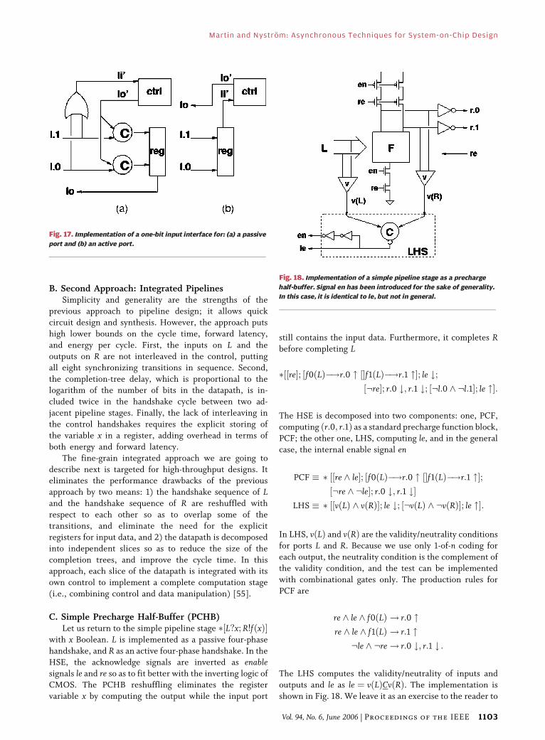
B. Second Approach: Integrated PipelinesSimplicity and generality are the strengths of the
previous approach to pipeline design; it allows quick
circuit design and synthesis. However, the approach puts
high lower bounds on the cycle time, forward latency,
and energy per cycle. First, the inputs on L and the
outputs on R are not interleaved in the control, putting
all eight synchronizing transitions in sequence. Second,
the completion-tree delay, which is proportional to thelogarithm of the number of bits in the datapath, is in-
cluded twice in the handshake cycle between two ad-
jacent pipeline stages. Finally, the lack of interleaving in
the control handshakes requires the explicit storing of
the variable x in a register, adding overhead in terms of
both energy and forward latency.
The fine-grain integrated approach we are going to
describe next is targeted for high-throughput designs. Iteliminates the performance drawbacks of the previous
approach by two means: 1) the handshake sequence of Land the handshake sequence of R are reshuffled with
respect to each other so as to overlap some of the
transitions, and eliminate the need for the explicit
registers for input data, and 2) the datapath is decomposed
into independent slices so as to reduce the size of the
completion trees, and improve the cycle time. In thisapproach, each slice of the datapath is integrated with its
own control to implement a complete computation stage
(i.e., combining control and data manipulation) [55].
C. Simple Precharge Half-Buffer (PCHB)Let us return to the simple pipeline stage ½L?x; R!fðxÞ�
with x Boolean. L is implemented as a passive four-phase
handshake, and R as an active four-phase handshake. In the
HSE, the acknowledge signals are inverted as enablesignals le and re so as to fit better with the inverting logic ofCMOS. The PCHB reshuffling eliminates the register
variable x by computing the output while the input port
still contains the input data. Furthermore, it completes Rbefore completing L
½re�; f0ðLÞ�!r:0 " ½�f 1ðLÞ�!r:1 "½ �; le #;½½:re�; r:0 #; r:1 #; ½:l:0 ^ :l:1�; le "�:
The HSE is decomposed into two components: one, PCF,
computing ðr:0; r:1Þ as a standard precharge function block,
PCF; the other one, LHS, computing le, and in the general
case, the internal enable signal en
PCF � ½re ^ le�; f 0ðLÞ�!r:0 " ½�f1ðLÞ�!r:1 "½ �;½½:re ^ :le�; r:0 #; r:1 #�
LHS � vðLÞ ^ vðRÞ½ �; le #; :vðLÞ ^ :vðRÞ½ �; le "½ �:
In LHS, vðLÞ and vðRÞ are the validity/neutrality conditions
for ports L and R. Because we use only 1-of-n coding for
each output, the neutrality condition is the complement of
the validity condition, and the test can be implemented
with combinational gates only. The production rules for
PCF are
re ^ le ^ f 0ðLÞ ! r:0 "re ^ le ^ f 1ðLÞ ! r:1 "
:le ^ :re ! r:0 #; r:1 # :
The LHS computes the validity/neutrality of inputs and
outputs and le as le ¼ vðLÞCvðRÞ. The implementation is
shown in Fig. 18. We leave it as an exercise to the reader to
Fig. 17. Implementation of a one-bit input interface for: (a) a passive
port and (b) an active port.
Fig. 18. Implementation of a simple pipeline stage as a precharge
half-buffer. Signal en has been introduced for the sake of generality.
In this case, it is identical to le, but not in general.
Martin and Nystrom: Asynchronous Techniques for System-on-Chip Design
Vol. 94, No. 6, June 2006 | Proceedings of the IEEE 1103

check that the PCHB reshuffling is indeed a half-buffer bychecking that the sequential composition of two PCHBs is a
full-buffer, i.e., the handshake on L can terminate even
when the right environment is blocked. The PCHB has
short forward latencyVonly two elementary transitions,
and pipelines composed of PCHBs have excellent through-
put (an average of 18 elementary transitions for the
MiniMIPS [28]).
D. General PCHB SchemeFor a general PCHB template with multiple input ports
and output ports, the implementation is as follows.
1) Each data rail rj of output port R depending on
inputs L1; . . . ; Lm is the output of a precharge
function block
rj ¼ PCF FjðL1; . . . ; LmÞ; enR; re� �
:
where enR is the internal enable computed by the
LHS circuit as follows, and re is the enable rail of R.
2) For each input port Li, the (inverted) left-enable
li:e is the C-element combination of the validity
of Li and the validity of all outputs Rk that dependon Li in the current iteration. For unconditional
outputs R1; R2; . . . ; Rk depending on Li, we have
li:e ¼ vðLiÞCvðR1ÞCvðR2Þ . . . CvðRkÞ:
The different left-enable computations often share
common parts. For instance, if two inputs Li and Lj
are needed by the same group of outputs, the
validity of that group of outputs can be shared by lei
and lej. [See Fig. 19(a).]
3) The internal enable signal enR is the C-element
combination of all left-enable signals li:e:
enR ¼ l1:eCl2:e . . . Clm:e:
4) When an input L is used conditionally, and the
condition is not provided by a control input, the
function block computes the condition as an extra
output, say, c:0; c:1 where c:0 indicates that L is
used, and c:1 that it is not used. The computation
of the left enable le is then done as in Fig. 19(b).5) Similarly, if a precharge function block does not
produce an output for some values of the inputs, a
pseudo output is produced for those values of the
input so that the validity of the output can be
generated in all cases.
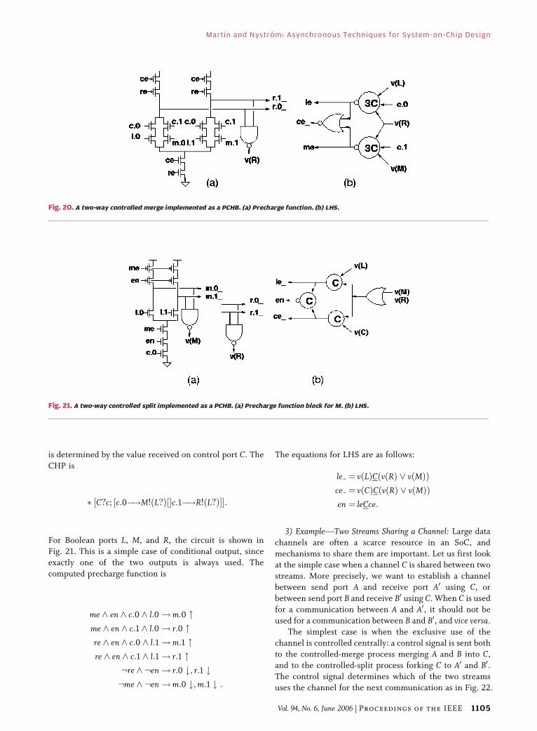
E. Split and Merge ComponentsControlled split and controlled merge are important
network components. They are also examples of PCHB
with conditional inputs and conditional outputs. Twosolutions are presented, a PCHB implementation and a
slack-zero implementation.
1) Half-Buffer Controlled Merge: A two-way controlled
merge merges two input streams from input ports L and Minto an output stream on port R. Which port to select for
the next input communication is determined by the value
received on control port C. The CHP is
C?c; c:0�!R!ðL?Þ½�c:1�!R!ðM?Þ½ �½ �:
For Boolean ports L, M, and R, the circuit is shown in
Fig. 20. The general scheme presented in the previous
section has been slightly optimized: the enable signal ce of
the control port C can be used as internal enable signal. The
computed precharge function is
ce ^ re ^ ðc:0 ^ l:0 _ c:1 ^ m:0Þ ! r:0 "ce ^ re ^ ðc:0 ^ l:1 _ c:1 ^ m:1Þ ! r:1 "
:ce ^ :re ! r:0 #; r:1 # :
The left enables and internal enable are computed as
le ¼ vðLÞCvðRÞCc:0
me ¼ vðMÞCvðRÞCc:1
ce ¼ le _ me:
2) Half-Buffer Controlled Split: The two-way controlled
split receives data on one input port L and sends it on one
of two output ports M and R. Which output port is selected
Fig. 19. Left-enable computation for a general PCHB scheme. (a) LHS
when all inputs needed for Rk are unconditional. (b) LHS when one
input Li is conditional. Control signals c.0 (BLi is used[) and c.1 (BLi is not
used[) may have to be generated as extra outputs.
Martin and Nystrom: Asynchronous Techniques for System-on-Chip Design
1104 Proceedings of the IEEE | Vol. 94, No. 6, June 2006
is determined by the value received on control port C. The
CHP is
C?c; c:0�!M!ðL?Þ½�c:1�!R!ðL?Þ½ �½ �:
For Boolean ports L, M, and R, the circuit is shown inFig. 21. This is a simple case of conditional output, since
exactly one of the two outputs is always used. The
computed precharge function is
me ^ en ^ c:0 ^ l:0 !m:0 "me ^ en ^ c:1 ^ l:0 ! r:0 "re ^ en ^ c:0 ^ l:1 !m:1 "re ^ en ^ c:1 ^ l:1 ! r:1 "
:re ^ :en ! r:0 #; r:1 #:me ^ :en !m:0 #;m:1 # :
The equations for LHS are as follows:
le ¼ vðLÞC vðRÞ _ vðMÞð Þce ¼ vðCÞC vðRÞ _ vðMÞð Þen ¼ leCce:
3) ExampleVTwo Streams Sharing a Channel: Large data
channels are often a scarce resource in an SoC, and
mechanisms to share them are important. Let us first lookat the simple case when a channel C is shared between two
streams. More precisely, we want to establish a channel
between send port A and receive port A0 using C, or
between send port B and receive B0 using C. When C is used
for a communication between A and A0, it should not be
used for a communication between B and B0, and vice versa.
The simplest case is when the exclusive use of the
channel is controlled centrally: a control signal is sent bothto the controlled-merge process merging A and B into C,
and to the controlled-split process forking C to A0 and B0.The control signal determines which of the two streams
uses the channel for the next communication as in Fig. 22.
Fig. 20. A two-way controlled merge implemented as a PCHB. (a) Precharge function. (b) LHS.
Fig. 21. A two-way controlled split implemented as a PCHB. (a) Precharge function block for M. (b) LHS.
Martin and Nystrom: Asynchronous Techniques for System-on-Chip Design
Vol. 94, No. 6, June 2006 | Proceedings of the IEEE 1105

VII. ASYNCHRONOUS BUSES
The previous case is a simple version of a bus. A bus is a many-
to-one merge of data streams, or a one-to-many split of data
streams, or a combination of both. (See Fig. 23.) In a micro-
processor, for example, buses are used to send the parameters
of an instruction from the register file to the different
execution units, or to send the results of an instructionexecution from an execution unit to the register file. In that
case, the control inputs to the merge and split components of
the bus are produced by the instruction decoder.
There are many implementations of asynchronous
buses. We show one based on the PCHB. The solution
brings to light an annoying problem in asynchronous
design: the efficient CMOS implementation of an n-input
nor gate when n is large. All solutions we know for themerge/split design contain at least one n-input nor-gate,
where n is either the number of merge inputs or the
number of split outputs.
Direct implementation is impossible because of the
CMOS restriction on the length of p-transistor pull-up
chains. Distributed implementations as trees of two-input
or-gates is possible without hazard because only one input
is exercised at a time, but it seriously taxes the throughputof the bus.
A. PCHB Implementation of a Many-to-One BusThe PCHB implementation of a many-to-one bus is a
straightforward extension of the two-way merge. The bus
has n data input ports L0 through Ln�1, a 1-of-N control
input C used to select an input port, and one data outputport R. The equations for the left-enables lk:e for k from 0
to n � 1, and for the internal enable are as follows:
lk:e ¼ vðLkÞCvðRÞCc:k
ce ¼_
k : 0::n � 1 : lk:e� �
en ¼ ce:
The implementation is shown in Fig. 24.
B. PCHB Implementation of a One-to-Many BusThe PCHB implementation of a one-to-many bus is a
straightforward extension of the two-way split. The bus has
n data output ports R0 through Rn�1, a 1-of-N control input
C used to select an output port, and one data input port L.
We choose the following implementation for the left-
enables and internal enable (others are possible):
ce ¼_
k : 0::n � 1 : vðRkÞCc:k� �
le ¼ ce CvðLÞen ¼ le:
The implementation is shown in Fig. 25.
Fig. 22. Two streams sharing channel C under control of dual-rail
signal cA, cB.
Fig. 23. A many-to-many bus composed of a many-to-one merge and a
one-to-many split.
Fig. 24. A PCHB implementation of a many-to-one bus. The triangles
marked with a letter v are combinational gates computing the validity
test of input ports L0 through Ln�1 and single output port R with bit
lines R:0 through R:k � 1.Observe that port C does not need an explicit
validity test.
Martin and Nystrom: Asynchronous Techniques for System-on-Chip Design
1106 Proceedings of the IEEE | Vol. 94, No. 6, June 2006

VIII . ARBITRATION
All circuits presented in the previous sections have stable
and noninterfering PR sets. But in order to implement
selections in which the conditions are not mutually
exclusive (nondeterministic choice), for instance, to select
between an external interrupt signal and the internal
Bnext-instruction[ signal in a microprocessor, or for
synchronization between the clocked components of a
GALS system, at least one operator must provide a non-deterministic choice between two true guards.
Since stability and noninterference are equivalent to
determinism, a nondeterministic computation does not
admit stable and noninterfering circuit implementation.
Therefore, any implementation of a nondeterministic
computation contains nonmonotonic transitions that
require special nondigital solutions. Those special circuits
are encapsulated inside two primitive building blocks: thearbiter and the synchronizer.
A fundamental, and long misunderstood, issue related
to implementing a nondeterministic choice is that of
metastability. In classical physics, it is impossible to put an
upper bound on the time it takes for a device to make a
nondeterministic decision between two alternatives.
When the system starts in a state where the physical
parameters are such that either alternative can be selected,the device may enter a metastable state in which it may
stay an arbitrary length of time before deciding one way or
the other [6].
A. Basic ArbiterThe simplest device to make a selection between non-
exclusive guards is the basic arbiter, or mutual exclusionelement. Its HSE specification is
arb � ½½x�!u "; ½:x�; u #jy�!v "; ½:y�; v #��
where x and y are simple Boolean variables. (The Bthin bar[j indicates that the two guards can be true at the same timeand thus that arbitration between the guards is needed.)
The arbiter is usually represented as in Fig. 26(a). Initially,
:u ^ :v holds. When either x or y or both become true,
either u or v is raised but not both. After u is raised the
environment resets x to false, and similarly if v is raised.
After x has been observed to be low, u is lowered; and
similarly if v was raised. Hence, if :u ^ :v holds initially,
:u _ :v holds at any time.The proper operation of the arbiter requires that two
inputs be stable, i.e., once x or y has been evaluated to true, itremains true at least until an acknowledgment transition takesplace. If one of the requests is withdrawn before the arbiter hasproduced an output, the arbiter may fail: one or both outputsmay glitch.
B. Implementation and MetastabilityLet us first consider the PR sets for arb that contain
unstable rules. The PR set for the Bunstable arbiter[ (inwhich u and v have been replaced with their inverses uand v ) is as follows:
x ^ v ! u #y ^ u ! v #
:x _ :v ! u ":y _ :u ! v " :
Fig. 25. A PCHB implementation of a one-to-many bus. The triangles
marked with a letter v are combinational gates computing the validity
test of input port L with bit lines L:0 through L:k � 1 and output ports
R0 through Rn�1.
Fig. 26. (a) The simple arbiter or mutual-exclusion element selects
between two possibly concurrent inputs x and y and produces
mutually exclusive outputs u and v. (b) An implementation of the basic
arbiter consisting of two cross-coupled NAND-gates and a filter. The
filter eliminates the spurious values of the NAND-gates outputs
produced during the metastable state.
Martin and Nystrom: Asynchronous Techniques for System-on-Chip Design
Vol. 94, No. 6, June 2006 | Proceedings of the IEEE 1107

The first two PRs of the arbiter are unstable and can fireconcurrently. In the digital domain, when started in the
state with x ^ y and :u ^ :v , the set of PRs specifying the
arbiter may produce the unbounded sequence of firings:
½ðu #; v #Þ; ðu "; v "Þ�:In the analog domain, the state of the arbiter in which x
and y are true and the voltages of both u and v are half-
way between Vdd and ground is called metastable. Nodes
u and v may oscillate and then stabilize to a commonintermediate voltage value for an unbounded period.
Eventually, the inherent asymmetry of the physical
realization (impurities, fabrication flaws, thermal noise,
etc.) will force the system into one of the two stable states
where u 6¼ v . But there is no upper bound on the time the
metastable state will last, which means that it is impossible
to include an arbitration device into a clocked system with
absolute certainty that a timing failure cannot occur.In order to eliminate the spurious values of u and v
produced during the metastable state, we compose the
Bbare[ arbiter with a filter taking u and v as input and
producing u and v as Bfiltered outputs.[ (An nMOS
implementation of filter is shown in [47]. The complete
nMOS circuit for the arbiter is described in [45]. A CMOS
version appeared first in [25].)
(In the CMOS construction of the filter shown inFig. 26(b), we use the threshold voltages to our advantage:
the channel of transistor t1 is conducting only when
ð:u ^ v Þ holds, and the channel of transistor t2 is
conducting only when ð:v ^ u Þ holds.) In QDI design,
the correct functioning of a circuit containing an arbiter is
independent of the duration of the metastable state;
therefore, relatively simple implementations of arbiters
can be used. In synchronous design, however, the imple-mentations have to meet the additional constraint that the
probability of the metastable state lasting longer than the
clock period should be negligible.
C. Channel ArbiterIf a process has to arbitrate between two nonmutually
exclusive channels, A and B, the channel arbiter CARB
serves as an interface to provide mutually exclusivechannels A0 and B0
½ A�!A0; AjB�!B0; B�½ �:
Since A and B are probed, they are implemented with a
passive handshake, and A0 and B0 with an active handshake.
The circuit is shown in Fig. 27. The previous design can be
used to arbitrate between channels with data. The arbiter
takes as inputs a signal from each data channel A and Bindicating that the channel has valid data. If a dual-rail code
is used, it suffices to look at the validity of a single bit (a
simple or-gate of the rails of the bit). C-elements prevent
the propagation of the data until the channel has been
selected by the arbiter.
D. Multiplexed ArbitrationA useful building block, the multiplexed arbiter XARB,
is an extension of the channel arbiter with a multiplexer
(merge)
½ A�!S; AjB�!S; B�½ �:
It is obtained by combining the channel arbiter CARB with
a simple multiplexer (merge). The multiplexed arbiter
XARB is shown in Fig. 28.
E. Multichannel Tree ArbiterThanks to the multiplexed arbiter XARB, we can
generalize the simple channel arbiter to the case of more
than two channels. The implementation of four-channelarbiter ARB4 as an arbiter tree is shown in Fig. 29. The
generalization to an arbitrary number of channels is
straightforward. The tree need not be balanced, and can
be incomplete if the number of channels is not a power
of two.
F. SynchronizerAs we argued earlier, the proper operation of the
arbiter requires that the inputs x and y be stable, i.e., oncethey are true, they remain asserted until the arbiter has
raised one of the corresponding outputs. Therefore, we
cannot use an arbiter to sample a completely unsynchro-
nized external signal, like an interrupt signal or other
Fig. 27. A slack-zero channel arbiter. The NAND-gates prevent the
second of two requests from proceeding before the HS of the first one
is completed.
Fig. 28.A multiplexed arbiter XARB composed of a channel arbiter and
a simple multiplexer.
Martin and Nystrom: Asynchronous Techniques for System-on-Chip Design
1108 Proceedings of the IEEE | Vol. 94, No. 6, June 2006

peripheral signal. A circuit to solve this problem is called a
synchronizer. The synchronizer has two inputs: a control
input re and the input signal x that is to be sampled. We
have chosen to specify it in such a way that it produces a
dual-rail output ðr:0; r:1Þ with the two rails representing
the true and false values of the sampled input x. The HSEspecification of the synchronizer is
sync � ½½re ^ :x�!r:0 "; ½:re�; r:0 #jre ^ x�!r:1 "; ½:re�; r:1 #��:
When the environment raises re, the synchronizer startsevaluating x and returns the observed value by raising
either r:0 or r:1. The difficulty is that x may change its value
at any time and therefore also during its evaluation by the
synchronizer. (That is the reason why both guards can
evaluate to true, which explains the use of the thin bar.) If xhas a stable true value within a finite, bounded interval
around the time re is raised, the synchronizer asserts r:1,
and similarly if x is a stable false; otherwise, the circuitasserts either r:1 or r:0, but not both. In practice, the
Bconfusion interval[ is a very short period, approximately
the delay of the single inverter used to invert the input. But
the synchronizer must work correctlyVi.e., raise either r:1or r:0Veven when x changes during the confusion interval.
Implementing a synchronizer properly is difficult enough
that it is usually avoided.
Unlike the arbiter, the synchronizer as defined by synccannot be implemented directly by feeding the two inputs
into a bistable device (cross-coupled nand gates). To see
why, consider that the program has to do two things to
advance from waiting for re ^ x to r:0 ": first, the second
guard must be Blocked out,[ so that r:1 cannot happen;
second, the assignment r:0 " must take place. But if xshould change after the second guard has been locked out
but before the first guard has been selected, the programwill deadlock. There is a race condition due to the fact that
the two guards can be invalidated at any time. Removing
the race condition requires introducing intermediate stablevariables a:0 and a:1 (they remain true once evaluated to
true) to stabilize the selection of one of the two guards,
leading to HSE sync1
½½re ^ :x ! a:0 "; ½a:0�; r:0 "; ½:re�; a:0 #; ½:a:0�; r:0 #jre ^ x ! a:1 "; ½a:1�; r:1 "; ½:re�; a:1 #; ½:a:1�; r:1 #��:
We decompose sync1 into three parts: int0 and int1
Bintegrate[ the possibly oscillating values of x into a stable
false value a:0 and a stable true value a:1, and SEL selects
between a:0 and a:1
int0 � ½re ^ :x�!a:0 "; ½:re�; a:0 #�½ �;int1 � ½re ^ x�!a:1 "; ½:re�; a:1 #�½ �;SEL � ½½a:0�!r:0 "; ½:a:0 ^ :a:1�; r:0 #
ja:1�!r:1 "; ½:a:1 ^ :a:0�; r:1 #��:
The parallel composition of int0, int1, and SEL is not
strictly equivalent to sync1 because, in the decomposition,
the control can advance simultaneously to a:0 " and a:1 ",
which is not possible in the original sync1. Consequent-
ly, the arbitration takes place between a:0 and a:1 in SEL.
But now the arbitration is between stable signals. However,
SEL is not exactly an arbiter: in an arbiter, when both inputs
are asserted, the arbiter selects both of them in an arbitraryorder, since a request is never withdrawn. In SEL, when
both inputs are asserted, only one should be selected:
whichever is chosen to be the value of the input when it is
sampled. Hence, SEL must check that both a:0 and a:1 are
false before resetting the output r:0 or r:1.
Nevertheless SEL can be implemented directly as a
bistable device in the same way as the arbiter. The
production rules for the bistable component are
r:1 ^ a:0 ! r:0 #:r:1 _ ð:a:0 ^ :a:1Þ ! r:0 "
r:0 ^ a:1 ! r:1 #:r:0 _ ð:a:1 ^ :a:0Þ ! r:1 " :
Fig. 29. A four-way tree arbiter composed of two multiplexed arbiters and a bare arbiter as the root. The generalization to an arbitrary number
of channels is straightforward. The tree need not be balanced, and can be incomplete if the number of channels is not a power of two.
Martin and Nystrom: Asynchronous Techniques for System-on-Chip Design
Vol. 94, No. 6, June 2006 | Proceedings of the IEEE 1109

The complete circuit for the synchronizer comprising the
two integrators, the bistable device and the metastability
filter is shown in Fig. 30. This is only one in a family ofsolutions [39]. A completely different solution is proposed
in [43].
G. A Clock/Handshake InterfaceThe following case study is a remarkable circuit that
interfaces a clock signal with a handshake protocol. More
precisely, the circuit transforms a clock signal � into ahandshake protocol between variables ro and ri. The HSE
of the clock/handshake interface (CHI) is
½:��; ro "; ½ri�; ½��; ro #; ½:ri�½ �:
If we introduce two integrators to generate stable copies xtand xf of the true and false values of �, the HSE becomes
½:ri ^ :xt ^ :xf �; ro "; ½ri ^ xt ^ xf �; ro #½ �:
which is just a three-input C-element. A conceptual
implementation of CHI is shown in Fig. 31.
The integrators may not work correctly for any input
waveform on �. For instance, a very slow rising xt could
trigger the C-element well before the voltage on xt reaches
Vdd. In this case, we should have to depend on a timing
assumption to guarantee that xt reaches Vdd before xfswitches; otherwise, the intermediate voltage could be
interpreted as false by the C-element later. This potential
analog problem can be removed by adding inverters on the
xt and xf outputs implemented as Schmitt triggers. We are
using the property of the Schmitt trigger that if the input
changes monotonically from one logic value to the other,
the output switches quickly from one value to the other.
Since the integrators see to it that the outputs changemonotonically regardless of the inputs, the Schmitt
triggers guarantee that xt and xf switch quickly enough
that neither node is observed as both true and false. This
(practical) implementation is shown in Fig. 32.
IX. GALS AND ASYNCHRONOUS-TO-SYNCHRONOUS CONVERSION
Historically, asynchronous communication between syn-chronous components was prevalent in computer systems.
For instance, the UNIBUS used in DEC PDP-11 and VAX
computers was a completely asynchronous bus [50], [51];
to this day, the common SCSI protocol for peripheral
communications supports handshake-based asynchronous
signalling [54]. In the case of our concrete problem, the
situation is one where P communicates with Q through an
asynchronous middleman R (e.g., the UNIBUS). Thetransfer of data commences with P’s sending the data to R,
whence it proceeds to Q. The interface between P and R as
well as that between R and Q are both examples of an
asynchronous-synchronous (AS) crossing, and have similar
solutions. Because of the direction of data movement in
the example, the R � Q interface is somewhat more
complicated, which is why we will discuss it; the P � Rinterface can be inferred through simplification. In all thatfollows, except the section that specifically deals with
multiple inputs, we will be analyzing the simple case
Fig. 30. A synchronizer circuit consisting of two integrators
(producing stable copies a.1 and a.0 of x and its inverse), a
bistable device, and a filter.
Fig. 31. A conceptual implementation of the clock-handshake inter-
face. The two integrators produce stable copies of the clock and its
inverse; the 3-input C-element implements the four-phase handshake
and produces the control input for the integrators.
Fig. 32. A practical implementation of the clock-handshake interface.
The outputs of the integrators have been augmented with Schmitt-
trigger inverters to guarantee quick transitions on xt and xf, and the
inverter on the input of the bottom integrator has been eliminated.
Martin and Nystrom: Asynchronous Techniques for System-on-Chip Design
1110 Proceedings of the IEEE | Vol. 94, No. 6, June 2006

where there is one Basynchronous part[ that is sendingdata to another Bsynchronous part.[
The reason that the AS problem has confounded so
many system designers is simply this: when we are given to
synchronize asynchronous signals into a synchronous
environment with a free-running periodic clock, there is
an unavoidable tradeoff between data communications
latency and a probability of catastrophic system failure. If
the communications latency is reduced, then the proba-bility of catastrophic system failure increases, and if the
probability of catastrophic system failure is to be reduced,
we must yield some communications latency. This cannot
be avoided. Similarly, no matter how much communica-
tions latency we are willing to live with, some small degree
of catastrophic system failure remains. The problem cannotbe avoided with less drastic means than introducing a
scheme for stopping the clock (see below) or giving upsynchronous operation entirely (see the preceding sections
of this paper).
The choice of the word Bcatastrophic[ is deliberate.
The behavior of a synchronous system that has undergone
synchronization failure cannot be usefully bounded, except
probabilistically. Sometimes one can read in the literature
of some scheme where the inventor claims that he can
build a system that synchronizes an asynchronous signal toa clock with a known, finite latency, and either: 1) there is
no possibility of synchronization failure or 2) if synchro-
nization failure does occur, it will only take some definite,
benign form. Both alternatives are impossible, but it
sometimes takes some careful analysis to show why a
particular circuit fails to achieve them; not rarely is it the
case that while the circuit in question may not suffer
disastrous internal consequences due to a synchronizationfailure, but instead its output signals are not guaranteed to
satisfy setup and hold times imposed by the environment.
Such circuits are frequently useful, as they may increase
the amount of time available for metastability resolution,
but nevertheless, they cannot ever be completely reliable.
To repeat, all schemes that aim at finite-latency commu-nication with zero probability of catastrophic system failureare doomed. Therefore, let us state as a design principle at theoutset that as part of the design of any scheme for AS con-version, the designer must identify, and ideally evaluate theprobability of, the scenario in which the system will fail cat-astrophically; as the problem cannot be avoided, it does nogood to sweep it under the rug.
1) Asynchronous-Synchronous Interface Using Two-PhaseNonoverlapping Clocks: Consider a synchronous system thatoperates off two-phase (�0 and �1 and their inverses)
nonoverlapping clocks. This is the standard method of
designing custom CMOS circuits and is treated in detail by
Mead and Conway [31] and Glasser and Dobberpuhl [56].
By means that do not concern us at the moment, two
phases of the clock are generated such that the predicate
:�0;i _ :�1;j holds in all locations i, j of the system where
the clock phases are available. In other words, it is never
the case that both clock phases are high, even taking clock
skew into account. Normally the clock generator is built onchip, but it is also possible to put it off chip, if we can
tolerate the extra pins; the advantage of putting the clock
generator off chip is that we can adjust the nonoverlap
time between the phases to compensate for unexpected
skews in the manufactured part.
While it is generally better to use four-phase
handshakes in asynchronous systems because of the
simplicity of implementation, the situation is not as clearin synchronous systems. We will study the data transfer
between a four-phase QDI system and a standard single-
rail synchronous system, and in this case, the synchronous
side of the interface can more easily be implemented with
a two-phase handshake because we do not need to keep
track of the phase of the data. In fact, because of the timing
guarantees that it is possible to enforce using the clock, we
can use the two-phase Bpulse handshake[ used in APLcircuits (Section II)
½:d0 ^ :d1�; d0 " j d1 "½ �k ½d0 _ d1�; d0 #; d1 #½ �:
(We use the vertical thin bar j to denote nondeterministic
choice.) This handshake has the speed advantage of a two-
phase handshake and the circuit advantage of a four-phase
handshake that the data sense is always positive. A blockdiagram appears in Fig. 33. The variables a0, a1, and aerepresent a standard QDI bit-wide channel (the general-
ization of the circuit to a wider datapath is obvious). The
variables sd and sv represent data and validity (inverted for
convenience) for a single-rail handshake channel, and of
course �0 and �1 represent the two clock phases. Fig. 34
shows how we would use the interface in a standard clocked
system (logic between the �1 latch and the �0 latch is notshown but could be present).
As long as sv obeys the synchronous timing discipline,
i.e., as long as sv is stable or falls to zero during �1, the
synchronous access to the data value sd presents no
Fig. 33. Block diagram of interface between four-phase QDI and two-
phase synchronous pulse handshakes.
Martin and Nystrom: Asynchronous Techniques for System-on-Chip Design
Vol. 94, No. 6, June 2006 | Proceedings of the IEEE 1111
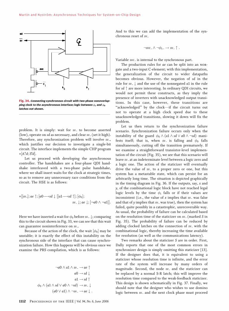
problem. It is simply: wait for sv to become asserted
(low), operate on sd as necessary, and clear sv (set it high).Therefore, any synchronization problem will involve sv ,
which justifies our decision to investigate a single-bit
circuit. The interface implements the simple CHP program
½A?d; S!d�.Let us proceed with developing the asynchronous
controller. The handshakes are a four-phase QDI hand-
shake interleaved with a two-phase pulse handshake,
where we shall insert waits for the clock at strategic times,so as to remove any unnecessary race conditions from the
circuit. The HSE is as follows:
½sv �; ae "; ½a0�!sd # ½�a1�!sd "�; ½�0�;½sv #; ae #; ½:a0 ^ :a1��:
Here we have inserted a wait for �0 before sv #; comparing
this to the circuit shown in Fig. 33, we can see that this wait
can guarantee noninterference on sv .
Because of the action of the clock, the wait ½�0� may be
unstable; it is exactly the effect of this instability on the
synchronous side of the interface that can cause synchro-nization failure. How this happens will be obvious once we
examine the PRS compilation, which is as follows:
:a0 ^ a1 ^ sv ! ae "a0 ! sd #a1 ! sd "
�0 ^ ða1 ^ sd _ a0 ^ :sdÞ ! sv #ða0 _ a1Þ ^ :sv ! ae # :
And to this we can add the implementation of the syn-chronous reset of sv
:svc ^ :�1 ! sv " :
Variable svc is internal to the synchronous part.
The production rules for ae can be split into an nor-
gate and a two-input C-element; with this implementation,the generalization of the circuit to wider datapaths
becomes obvious. However, the negation of sd in the
rule for sv # and the use of the nonnegated a1 in the rule
for sd " are more interesting. In ordinary QDI circuits, we
would not permit these constructs, as they imply the
presence of inverters with unacknowledged output transi-
tions. In this case, however, these transitions are
Backnowledged[ by the clockVif the circuit turns outnot to operate at a high clock speed due to these
unacknowledged transitions, slowing it down will fix the
problem.
Let us then return to the synchronization failure
scenario. Synchronization failure occurs only when the
instability of the guard �0 ^ ða1 ^ sd _ a0 ^ :sdÞ mani-
fests itself; that is, when sv is falling and �0 falls
simultaneously, cutting off the transition prematurely. Ifwe examine a straightforward transistor-level implemen-
tation of the circuit (Fig. 35), we see that this scenario will
leave sv at an indeterminate level between a logic zero and
a logic one. The action of the staticizer will eventually
drive the value of sv to a proper zero or one, but this
system has a metastable state, which can persist for an
arbitrarily long time. The situation is depicted graphically
in the timing diagram in Fig. 36. If the outputs, say, x andy, of the combinational logic block have not reached legal
logic levels by the time �1 falls or if their values are
inconsistent (i.e., the value of x implies that sv was false
and that of y implies that sv was true), then the system has
failed, quite possibly in a catastrophic, unrecoverable way.
As usual, the probability of failure can be calculated based
on the resolution time of the staticizer on sv (marked S in
Fig. 35). The probability of failure can be reduced byadding clocked latches on the connection of sv with the
combinational logic, thereby increasing the time available
for resolution (as well as the communications latency).
Two remarks about the staticizer S are in order. First,
Dally reports that one of the most common errors in
synchronizer design is simply omitting this staticizer [13].
If the designer does that, it is equivalent to using a
staticizer whose resolution time is infinite, and the errorrate of the system will increase by many orders of
magnitude. Second, the node sv and the staticizer can
be replaced by a normal S-R latch; this will improve the
resolution time compared to the weak-feedback staticizer.
This design is shown schematically in Fig. 37. Finally, we
should note that the designer who wishes to use domino
logic between sv and the next clock phase must proceed
Fig. 34. Connecting synchronous circuit with two-phase nonoverlap-
ping clock to the asynchronous interface; logic between ��1 and ��0
latches not shown.
Martin and Nystrom: Asynchronous Techniques for System-on-Chip Design
1112 Proceedings of the IEEE | Vol. 94, No. 6, June 2006
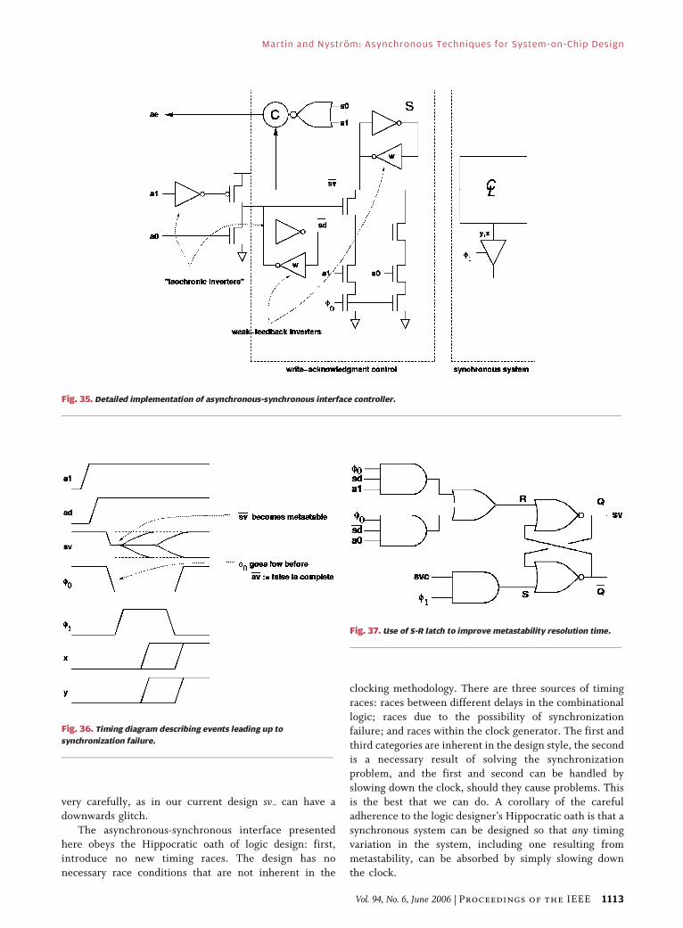
very carefully, as in our current design sv can have a
downwards glitch.
The asynchronous-synchronous interface presentedhere obeys the Hippocratic oath of logic design: first,
introduce no new timing races. The design has no
necessary race conditions that are not inherent in the
clocking methodology. There are three sources of timing
races: races between different delays in the combinational
logic; races due to the possibility of synchronization
failure; and races within the clock generator. The first and
third categories are inherent in the design style, the secondis a necessary result of solving the synchronization
problem, and the first and second can be handled by
slowing down the clock, should they cause problems. This
is the best that we can do. A corollary of the careful
adherence to the logic designer’s Hippocratic oath is that a
synchronous system can be designed so that any timing
variation in the system, including one resulting from
metastability, can be absorbed by simply slowing downthe clock.
Fig. 35. Detailed implementation of asynchronous-synchronous interface controller.
Fig. 36. Timing diagram describing events leading up to
synchronization failure.
Fig. 37. Use of S-R latch to improve metastability resolution time.
Martin and Nystrom: Asynchronous Techniques for System-on-Chip Design
Vol. 94, No. 6, June 2006 | Proceedings of the IEEE 1113

Finally, should the error probability of the circuit be
too high for comfort at the lowest clock rate we are willing
to tolerate, we can simply add additional latches where thesv wire enters the synchronous domain; this will bring the
probability of failure arbitrarily low, at the cost of adding
synchronization latency. In as simple a circuit as this one,
the extra latency also hurts the data throughput on the
synchronized channel, but with more sophisticated
techniques ([13], [47], [57] . . .), this can be avoided.
A. Stoppable-Clock GALSThe alternative to using synchronizers where the
asynchronous signal enters the clock domain is to permit
the asynchronous signal to stop the clock. In such a
scheme, the asynchronous part of the system can treat all
variables on the synchronous side as registers; as long as
the writes to the variables are complete when the
asynchronous side releases the clock, with the caveats
mentioned below, there is no risk of misbehavior.The idea behind stoppable, or pausable, clocks is to
build an oscillator whose every cycle involves an arbitra-
tion against an external request r. Every time the clock
wins the arbitration, it ticks; every time it loses, it stops
and waits for the asynchronous request to be withdrawn.
The circuit is shown schematically in Fig. 38; the grant gsignals to the asynchronous part that the clock is stopped
and the asynchronous part has exclusive access to sharedvariables (in this case, sv). Of course the arbiter itself
introduces the possibility of metastability, but in this case
the entire system simply waits for the metastability to be
resolved; neither the clock nor the asynchronous part of
the system is permitted to proceed until that happens.
Normally the delay is implemented with a string of
inverters, turning the stoppable-clock generator into a
stoppable ring oscillator.
1) Stoppable-Clock Asynchronous-Synchronous Interface:To complete the stoppable-clock interface, we need to
specify the clock oscillator, the clock generator, and the
asynchronous state machine for the data transfers. A block
diagram of the design is shown in Fig. 39. We keep thedesign as similar as possible to the synchronizer-based
described in Section IX-A. We assume a clock generator
of the type described by Mead and Conway [31]. We ar-
range it so that when the oscillator is in the stopped state
(�x low), �0 is high and �1 is low: this choice matches the
design of the synchronizer of Section IX-A. With this
choice, the specification of the asynchronous controller
becomes the following:
½:sv�; ae "; ½a0�!sd #; r " ½�a1�!sd "; r "�; ½g�;½sv "; ae #; ½:a0 ^ :a1�; r #; ½:g��:
It is possible to increase the performance of this design
slightly by postponing the wait for input neutrality,
½:a0 ^ :a1� so that it overlaps with the reset phase of the
arbiter, but the HSE we show here has a satisfyingly simple
implementation, shown in Fig. 40; it is identical to theasynchronous controller for the synchronizer-based solu-
tion, except that the C-element driving ae has one
additional input.
As is true of all the other asynchronous-synchronous
interfaces described in this paper, the single-rail data
encoding used on the synchronous side of the interface
introduces timing assumptions in the asynchronous side of
the interface. However, these timing assumptions canalways be satisfied by slowing down the clock speed,
exactly as in a synchronous system; in fact it is these timing
assumptions that are the defining characteristic of
synchronous design, as only delay-insensitive design styles
are free of such timing assumptions. It is important to keep
in mind the essential difference between this kind of
timing Brace[ and the unavoidable one that results from
the intrinsic nature of the requirement that data besynchronized with a free-running clock: the former type of
timing race can be satisfied by manipulating physical
parameters, usually in some obvious way; and the latter
type of timing race cannot under any circumstances be
avoided in its entirety as long as the clock-synchronization
requirement is maintained. The type of circuit described in
this section, as it does not attempt to synchronize data to a
free-running clock, is completely free of the latter type oftiming race.
2) Interfaces Using Edge-Triggered Methodology: In the
previous section, we explored the design of asynchronous-
synchronous interfaces using a clocking methodology with
multiphase nonoverlapping clocks. Similar designs are
possible if we are using edge-triggering clocks in our
synchronous methodology, but there are some subtleties tobear in mind, resulting from the timing characteristics of
edge-triggered flip-flops. Unlike the situation with non-
overlapping clocks, each edge-triggered memory element,
called an edge-triggered flip-flop, itself has a timing race.
Fig. 38. Safely stoppable clock oscillator.
Martin and Nystrom: Asynchronous Techniques for System-on-Chip Design
1114 Proceedings of the IEEE | Vol. 94, No. 6, June 2006
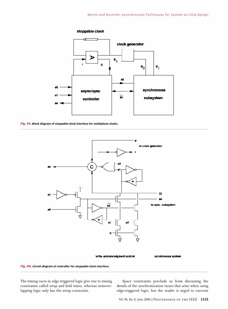
The timing races in edge-triggered logic give rise to timing
constraints called setup and hold times, whereas nonover-
lapping logic only has the setup constraint.
Space constraints preclude us from discussing the
details of the synchronization issues that arise when using
edge-triggered logic, but the reader is urged to exercise
Fig. 39. Block diagram of stoppable-clock interface for multiphase clocks.
Fig. 40. Circuit diagram of controller for stoppable-clock interface.
Martin and Nystrom: Asynchronous Techniques for System-on-Chip Design
Vol. 94, No. 6, June 2006 | Proceedings of the IEEE 1115

care. The most important difference between edge-
triggered logic and multiphase clocking is that there is a
time near each active clock edge at which inputs are not
permitted to change; contrast this with the situation in
multiphase systems, where each variable is required to be
quiescent only at the falling edge of the clock used tosample it and not at other clock edges. The simplest
solution is to use the inactive clock edges to drive the
asynchronous state machine and reserve the active clock
edge for the synchronous logic. With this in mind, it is
straightforward to derive correct synchronizers and
stoppable clocks for the edge-triggered methodology.
B. Using Stoppable Clocks With Multiple InterfacesIt is rarely interesting to design a GALS system where
modules have only one-way communication; it is as good
as always true that if module P sends module Q messages,
then it expects some sort of response (directly or
indirectly).
Where multiple interfaces are involved, building a
GALS system using synchronizers poses no new difficul-
ties. If we are using stoppable clocks, however, we need tointroduce a mechanism by which one or several asynchro-
nous subsystems can stop the clock of the synchronous
subsystem. To do this, we can combine the stoppable clock
generator of Fig. 37 with the multiplexed arbiter presented
in Section VIII-D, as shown in Fig. 41, where ARB1 is an
instance of the multiplexed arbiter, whereas ARB0 is the
normal arbiter used in the stoppable-clock generator.
From our earlier analysis of the multiplexed arbiter, weknow that at most one of g1 and g2 can be active at any
time; this arbiter sequences the accesses to the synchro-
nous logic block by the asynchronous units A1 and A2. It
is also true that the standard implementation of the arbi-
ter ARB0 in the clock generator is fair; therefore, if, say,
A0 initiates a data transfer while the master clock is high
and does not complete it within half a clock, the clock
will win the ARB0 arbitration as soon as the request r iswithdrawn. Therefore, slow asynchronous accesses to the
synchronous subsystem: 1) can occur only interspersed
with synchronous cycles and 2) are mutually exclusive.
A different implementation with multiple interfaces is
shown in Fig. 42. Here, the arbiters are arranged
sequentially instead of in a tree; both ARB0 and ARB1
are standard arbiters. The result of this is that A0 and A1
can access S at the same time. The drawback of thisapproach is that while it is simpler, it results in extra
delay in the clock generator; as long as desired clock
speeds are low and the number of external interfaces on Sis small, this delay can easily be compensated for by
changing the clock delay �, but in other cases, it may
become limiting. Accordingly, the tree arbiter is more
suitable for systems with many channels or high speeds. It
is possible, but difficult, to design a tree arbiter that canpermit multiple simultaneous access. (This problem is an
instance of Breaders and writers mutual exclusion.[)
Finally, Muttersbach et al. describe an implementation of
a shared-interface controller implemented with timing
assumptions [35].
C. Zero Probability of FailureWith Free-Running Clocks
While we have seen real advantages in the use of
stoppable clocks in GALS systems, it must be admitted
that most systems that can be called BGALS[ do not
actually use such clocks but instead use the more
traditional free-running-clock-and-synchronizers ap-
proach. One of the reasons for this was discovered by
researchers at ETH Zurich [58]: the control of delays by
use of an off-chip clock offers an extremely versatile andconvenient means for adjusting the clock speed; this is the
case because of all physical parameters (voltage, current,
Fig. 41. Sharing a stoppable clock from several interfaces;
tree arbiter version.
Fig. 42. Sharing a stoppable clock from several interfaces;
sequential arbitration version.
Martin and Nystrom: Asynchronous Techniques for System-on-Chip Design
1116 Proceedings of the IEEE | Vol. 94, No. 6, June 2006
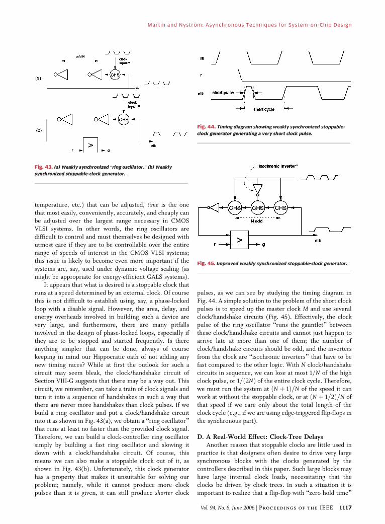
temperature, etc.) that can be adjusted, time is the one
that most easily, conveniently, accurately, and cheaply canbe adjusted over the largest range necessary in CMOS
VLSI systems. In other words, the ring oscillators are
difficult to control and must themselves be designed with
utmost care if they are to be controllable over the entire
range of speeds of interest in the CMOS VLSI systems;
this issue is likely to become even more important if the
systems are, say, used under dynamic voltage scaling (as
might be appropriate for energy-efficient GALS systems).It appears that what is desired is a stoppable clock that
runs at a speed determined by an external clock. Of course
this is not difficult to establish using, say, a phase-locked
loop with a disable signal. However, the area, delay, and
energy overheads involved in building such a device are
very large, and furthermore, there are many pitfalls
involved in the design of phase-locked loops, especially if
they are to be stopped and started frequently. Is thereanything simpler that can be done, always of course
keeping in mind our Hippocratic oath of not adding any
new timing races? While at first the outlook for such a
circuit may seem bleak, the clock/handshake circuit of
Section VIII-G suggests that there may be a way out. This
circuit, we remember, can take a train of clock signals and
turn it into a sequence of handshakes in such a way that
there are never more handshakes than clock pulses. If webuild a ring oscillator and put a clock/handshake circuit
into it as shown in Fig. 43(a), we obtain a Bring oscillator[that runs at least no faster than the provided clock signal.
Therefore, we can build a clock-controller ring oscillator
simply by building a fast ring oscillator and slowing it
down with a clock/handshake circuit. Of course, this
means we can also make a stoppable clock out of it, as
shown in Fig. 43(b). Unfortunately, this clock generatorhas a property that makes it unsuitable for solving our
problem; namely, while it cannot produce more clock
pulses than it is given, it can still produce shorter clock
pulses, as we can see by studying the timing diagram in
Fig. 44. A simple solution to the problem of the short clock
pulses is to speed up the master clock M and use several
clock/handshake circuits (Fig. 45). Effectively, the clock
pulse of the ring oscillator Bruns the gauntlet[ between
these clock/handshake circuits and cannot just happen toarrive late at more than one of them; the number of
clock/handshake circuits should be odd, and the inverters
from the clock are Bisochronic inverters[ that have to be
fast compared to the other logic. With N clock/handshake
circuits in sequence, we can lose at most 1=N of the high
clock pulse, or 1=ð2NÞ of the entire clock cycle. Therefore,
we must run the system at ðN þ 1Þ=N of the speed it can
work at without the stoppable clock, or at ðN þ 1=2Þ=N ofthat speed if we care only about the total length of the
clock cycle (e.g., if we are using edge-triggered flip-flops in
the synchronous part).
D. A Real-World Effect: Clock-Tree DelaysAnother reason that stoppable clocks are little used in
practice is that designers often desire to drive very large
synchronous blocks with the clocks generated by thecontrollers described in this paper. Such large blocks may
have large internal clock loads, necessitating that the
clocks be driven by clock trees. In such a situation it is
important to realize that a flip-flop with Bzero hold time[
Fig. 43. (a) Weakly synchronized Bring oscillator.[ (b) Weakly
synchronized stoppable-clock generator.
Fig. 44. Timing diagram showing weakly synchronized stoppable-
clock generator generating a very short clock pulse.
Fig. 45. Improved weakly synchronized stoppable-clock generator.
Martin and Nystrom: Asynchronous Techniques for System-on-Chip Design
Vol. 94, No. 6, June 2006 | Proceedings of the IEEE 1117
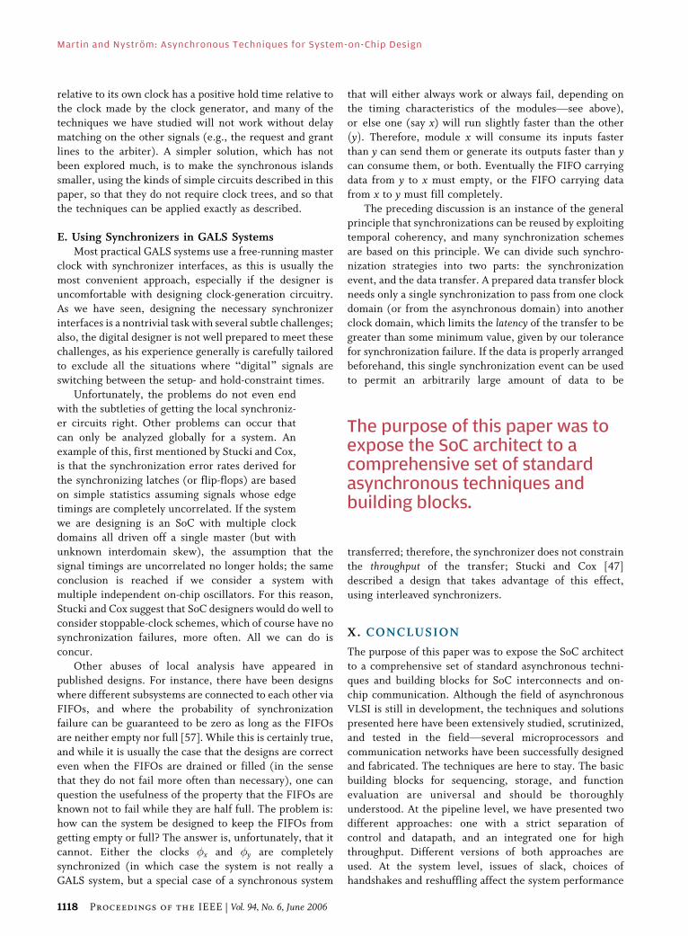
relative to its own clock has a positive hold time relative tothe clock made by the clock generator, and many of the
techniques we have studied will not work without delay
matching on the other signals (e.g., the request and grant
lines to the arbiter). A simpler solution, which has not
been explored much, is to make the synchronous islands
smaller, using the kinds of simple circuits described in this
paper, so that they do not require clock trees, and so that
the techniques can be applied exactly as described.
E. Using Synchronizers in GALS SystemsMost practical GALS systems use a free-running master
clock with synchronizer interfaces, as this is usually the
most convenient approach, especially if the designer is
uncomfortable with designing clock-generation circuitry.
As we have seen, designing the necessary synchronizer
interfaces is a nontrivial task with several subtle challenges;also, the digital designer is not well prepared to meet these
challenges, as his experience generally is carefully tailored
to exclude all the situations where Bdigital[ signals are
switching between the setup- and hold-constraint times.
Unfortunately, the problems do not even end
with the subtleties of getting the local synchroniz-
er circuits right. Other problems can occur that
can only be analyzed globally for a system. Anexample of this, first mentioned by Stucki and Cox,
is that the synchronization error rates derived for
the synchronizing latches (or flip-flops) are based
on simple statistics assuming signals whose edge
timings are completely uncorrelated. If the system
we are designing is an SoC with multiple clock
domains all driven off a single master (but with
unknown interdomain skew), the assumption that thesignal timings are uncorrelated no longer holds; the same
conclusion is reached if we consider a system with
multiple independent on-chip oscillators. For this reason,
Stucki and Cox suggest that SoC designers would do well to
consider stoppable-clock schemes, which of course have no
synchronization failures, more often. All we can do is
concur.
Other abuses of local analysis have appeared inpublished designs. For instance, there have been designs
where different subsystems are connected to each other via
FIFOs, and where the probability of synchronization
failure can be guaranteed to be zero as long as the FIFOs
are neither empty nor full [57]. While this is certainly true,
and while it is usually the case that the designs are correct
even when the FIFOs are drained or filled (in the sense
that they do not fail more often than necessary), one canquestion the usefulness of the property that the FIFOs are
known not to fail while they are half full. The problem is:
how can the system be designed to keep the FIFOs from
getting empty or full? The answer is, unfortunately, that it
cannot. Either the clocks �x and �y are completely
synchronized (in which case the system is not really a
GALS system, but a special case of a synchronous system
that will either always work or always fail, depending onthe timing characteristics of the modulesVsee above),
or else one (say x) will run slightly faster than the other
ðyÞ. Therefore, module x will consume its inputs faster
than y can send them or generate its outputs faster than ycan consume them, or both. Eventually the FIFO carrying
data from y to x must empty, or the FIFO carrying data
from x to y must fill completely.
The preceding discussion is an instance of the generalprinciple that synchronizations can be reused by exploiting
temporal coherency, and many synchronization schemes
are based on this principle. We can divide such synchro-
nization strategies into two parts: the synchronization
event, and the data transfer. A prepared data transfer block
needs only a single synchronization to pass from one clock
domain (or from the asynchronous domain) into another
clock domain, which limits the latency of the transfer to begreater than some minimum value, given by our tolerance
for synchronization failure. If the data is properly arranged
beforehand, this single synchronization event can be used
to permit an arbitrarily large amount of data to be
transferred; therefore, the synchronizer does not constrain
the throughput of the transfer; Stucki and Cox [47]
described a design that takes advantage of this effect,
using interleaved synchronizers.
X. CONCLUSION
The purpose of this paper was to expose the SoC architect
to a comprehensive set of standard asynchronous techni-
ques and building blocks for SoC interconnects and on-
chip communication. Although the field of asynchronous
VLSI is still in development, the techniques and solutions
presented here have been extensively studied, scrutinized,
and tested in the fieldVseveral microprocessors and
communication networks have been successfully designedand fabricated. The techniques are here to stay. The basic
building blocks for sequencing, storage, and function
evaluation are universal and should be thoroughly
understood. At the pipeline level, we have presented two
different approaches: one with a strict separation of
control and datapath, and an integrated one for high
throughput. Different versions of both approaches are
used. At the system level, issues of slack, choices ofhandshakes and reshuffling affect the system performance
The purpose of this paper was toexpose the SoC architect to acomprehensive set of standardasynchronous techniques andbuilding blocks.
Martin and Nystrom: Asynchronous Techniques for System-on-Chip Design
1118 Proceedings of the IEEE | Vol. 94, No. 6, June 2006

in a profound way. We have tried to make the designeraware of their importance. At the more fundamental level,
issues of stability, isochronic forks, validity, and neutrality
tests, state encoding must be understood in order for the
designer to avoid the recurrence of hazard malfunctions
that have plagued early attempts at asynchrony.
Many styles of asynchronous designs have been pro-
posed. They differ by the type and extent of the timing
assumptions they make. Rather than presenting andcomparing them all in a necessarily shallow way, we have
chosen to present the most Bdasynchronous[ approachVQDIVin some depth. While we realize very well that the
engineer of an SoC has the freedom and duty to make alltiming assumptions necessary to get the job done cor-
rectly, we also believe that, from a didactic point of view,
starting with the design style from which all others can be
derived is the most effective way of teaching this still
vastly misunderstood but beautiful VLSI design method. h
Acknowledgment
The authors would like to thank J. Dama, W. Jang,
M. Josephs, J. L. Martin, M. Naderi, K. Papadantonakis,
and P. Prakash for their excellent comments on the paper.
RE FERENCES
[1] The Basynchronous[ bibliography. (2004).[Online]. Available: http://www.win.tue.nl/async-bib/.
[2] H. C. Brearley, BILLIAC II: A shortdescription and annotated bibliography,[IEEE Trans. Comput., vol. C-14, no. 6,pp. 399–403, Jun. 1965.
[3] C. H. K. v. Berkel and R. Saejis, BCompilationof communicating processes into delay-in-sensitive circuits,[ Proc. Int. Conf. ComputerDesign (ICCD), 1988, pp. 157–162.
[4] E. Brunvand and R. F. Sproull, BTranslatingconcurrent programs into delay-insensitivecircuits,[ Dig. Tech. Papers 1989 IEEE Int.Conf. Computer-Aided Design, pp. 262–265.
[5] S. M. Bums and A. J. Martin, BSyntax-directedtranslation of concurrent programs intoself-timed circuits,[ in Advanced Researchin VLSI, J. Allen and F. Leighton, Eds.Cambridge, MA: MIT Press, 1988.
[6] T. J. Chaney and C. E. Molnar, BAnomalousbehavior of synchronizer and arbitercircuits,[ IEEE Trans. Comput., vol. C-22,no. 4, pp. 421–422, Apr. 1973.
[7] D. M. Chapiro, Globally-Asynchronous,Locally-Synchronous Systems, Ph.D.dissertation, Stanford Univ., Stanford,CA, 1984, Stanford CS Tech. Rep.STAN-CS-84-1026.
[8] T.-A. Chu, BSynthesis of self-timed VLSIcircuits from graph-theoretic specifications,[in Proc. Int. Conf. Computer Design (ICCD),1987, pp. 220–223.
[9] F.-C. Cheng, BPractical design andperformance evaluation of completiondetection circuits,[ in IEEE Int. Conf.Computer Design (ICCD), 1998, pp. 354–359.
[10] W. A. Clark, BMacromodular computersystems,[ in AFIPS Conf. Proc. 1967 SpringJoint Computer Conf., 1967, pp. 335–336.
[11] J. Cortadella et al., Logic Synthesis of Asynchro-nous Controllers and Interfaces. New York:Springer-Verlag, 2002.
[12] VV, BPetrify: A tool for manipulatingconcurrent specifications and synthesis ofasynchronous controllers,[ IEICE Trans.Inf. Syst., vol. E80-D, pp. 315–325, 1997.
[13] W. J. Dally and J. W. Poulton, Digital SystemsEngineering. Cambridge, U.K.: CambridgeUniv. Press, 1998.
[14] S. B. Furber et al., BA micropipelined ARM,[in Proc. VII Banff Workshop: AsynchronousHardware Design, 1993.
[15] VV, BAMULET2e: An asynchronousembedded controller,[ in Proc. Async ’97,1997, pp. 290–299.
[16] J. D. Garside, BProcessors,[ in Principles ofAsynchronous Circuit Design: A Systems
Perspective, J. Sparse and S. Furber, Eds.Boston, MA: Kluwer, 2001, ch. 15.
[17] H. v. Gageldonk et al., BAn asynchronouslow-power 80c51 microcntroller,[ Proc. Int.Symp. Advanced Research in AsynchronousCircuits and Systems, 1999, pp. 96–107.
[18] M. R. Greenstreet, BReal-time merging,[ inProc. Fifth Int. Symp. Advanced Research inAsynchronous Circuits and Systems: ASYNC99,Barcelona, Spain, 19–21 April 1999,Los Alamitos, CA: IEEE CS Press, 1999.
[19] C. A. R. Hoare, BCommunicating sequentialprocesses,[ Commun. ACM, vol. 21,pp. 666–677, 1978.
[20] D. A. Huffman, BThe synthesis of sequentialswitching circuits,[ in Sequential Machines:Selected Papers, E. F. Moore, Ed. Reading,MA: Addison-Wesey, 1964.
[21] C. Kelly, IV, V. Ekanyake, and R. Manohar,BSNAP: A sensor network asynchronousprocessor,[ Proc. Int. Symp. Advanced Researchin Asynchronous Circuits and Systems, 2003,pp. 24–35.
[22] A. M. Lines, BPipelined asynchronouscircuits,[ M.S. thesis, California Inst.Technol., Pasadena, 1997.
[23] R. Manohar and A. J. Martin, BQuasi-delay-insensitive circuits are turing-complete,[Proc. Int. Symp. Advanced Research inAsynchronous Circuits and Systems,Fukushima, Japan, 1996.
[24] A. J. Martin, BThe design of a self-timedcircuit for distributed mutual exclusion,[Proc. 1985 Chapel Hill Conf. VLSI, H. Fuchs,Ed., pp. 245–260.
[25] VV, BProgramming in VLSI: Fromcommunicating processes to self-timed VLSIcircuits,[ in Concurrent Programming (1987 UTYear of Programming Institute on ConcurrentProgramming), C. A. R. Hoare, Ed. Reading,MA.: Addison-Wesley, 1989.
[26] VV, BThe limitations to delay-insensitivityin asynchronous circuits,[ Proc. 6th MIT Conf.Advanced Research in VLSI, W. J. Dally, Ed.,1990, pp. 263–278.
[27] A. J. Martin et al., BThe design of anasynchronous microprocessor,[ Proc.Decennial Caltech Conf. Advanced Researchin VLSI, C. L. Seitz, Ed., 1991, pp. 351–373.
[28] VV, BThe Design of an Asynchronous MIPSR3000 Processor,[ in Proc. 17th Conf.Advanced Research in VLSI, Los Alamitos,CA: IEEE CS Press, 1997.
[29] A. J. Martin, BSynthesis method for self-timedVLSI circuits,[ in Proc. 1987 IEEE Int. Conf.Computer Design (ICCD 87), pp. 224–229.
[30] A. J. Martin, M. Nystrom, and C. G. Wong,BThree generations of asynchronousmicroprocessors,[ IEEE Des. Test Comput.
(Special Issue on Clockless VLSI Design),vol. 20, no. 6, pp. 9–17, Nov./Dec. 2003.
[31] C. Mead and L. Conway, Introduction to VLSISystems. Reading, MA: Addison-Wesley,1980.
[32] R. E. Miller, Switching Theory. New York:Wiley, 1965, vol. 2, ch. 10.
[33] D. E. Muller and W. S. Bartky, BA theory ofasynchronous circuits,[ Proc. Int. Symp.Theory of Switching, 1959, pp. 204–243.
[34] C. J. Myers, Asynchronous Circuit Design.New York: Wiley, 2001.
[35] J. Muttersbach, T. Villiger, and W. Fichner,BPractical design of globally-asynchronouslocally-synchronous systems,[ Proc. Int. Symp.Advanced Research in Asynchronous Circuitsand Systems, 2000, pp. 52–59.
[36] T. Nanya et al., BTITAC: Design of aquasi-delay-insensitive microprocessor,[IEEE Des. Test Comput., vol. 11, no. 2,pp. 50–63, Summer, 1994, IEEE.
[37] VV, BTITAC-2: A 32-bit scalable-delay-insensitive microprocessor,[ in Proc. HOTChips IX, 1997, pp. 19–32.
[38] S. M. Nowick, M. B. Josephs, and C. H.van Berkel, BSpecial issue: Asynchronouscircuits and systems,[ Proc. IEEE, vol. 87,no. 2, pp. 217–396, 1999.
[39] M. Nystrom and A. J. Martin, BCrossing thesynchronous-asynchronous divide,[ presentedat the Workshop Complexity Effective Design,Anchorage, AK, 2002.
[40] VV, Asynchronous Pulse Logic. Boston,MA: Kluwer, 2001.
[41] P. Prakash and A. J. Martin, BSlack matchingquasi-delay-insensitive circuits,[ in Proc. Int.Symp. Advanced Research in AsynchronousCircuits and Systems, 2006, pp. 195–204.
[42] M. Renaudin, P. Vivet, and F. Robin,BASPRO-216: A standard-cell QDI 16-bitRISC asynchronous microprocessor,[ Proc.Int. Symp. Advanced Research in AsynchronousCircuits and Systems, 1998, pp. 22–31.
[43] F. U. Rosenberger, C. E. Molnar, T. J. Chaney,and T.-P. Fang, BQ-modules: internallyclocked delay-insensitive modules,[ IEEETrans. Comput., vol. 37, no. 9, pp. 1005–1018,Sep. 1988.
[44] S. Rotem et al., BRAPPID: An asynchronousinstruction length decoder,[ Proc. Int. Symp.Advanced Research in Asynchronous Circuitsand Systems, 1999, pp. 60–70.
[45] C. L. Seitz, ‘‘System timing,[ in Introduction toVLSI Systems. Reading, MA: Addison-Wes-ley, 1980, ch. 7.
[46] J. Sparsø and S. Furber, Eds., Principlesof Asynchronous Circuit Design: A SystemsPerspective. Boston, MA: Kluwer, 2001.
Martin and Nystrom: Asynchronous Techniques for System-on-Chip Design
Vol. 94, No. 6, June 2006 | Proceedings of the IEEE 1119

[47] M. J. Stucki and J. J. Cox, BSynchronizationstrategies,[ in Proc. 1st Caltech Conf. VeryLarge Scale Integration, C. L. Seitz, Ed., 1979,pp. 375–393.
[48] I. E. Sutherland and S. Fairbanks, BGasP:A minimal FIFO control,[ in Proc. 10th Int.Symp. Advanced Research in AsynchronousCircuits and Systems, 2004, pp. 46–53.
[49] T. E. Williams and M. A. Horowitz, BAzero-overhead self-timed 160 ns 54 b CMOSdivider,[ IEEE J. Solid-State Circuits, vol. 26,no. 11, pp. 1651–1661, Nov. 1991.
[50] PDP-11 Peripherals and Interfacing Handbook,Digital Equipment Corp., Maynard, MA, 1971,DEC part no. 112-01071-1854 D-09-25.
[51] PDP-11 Bus Handbook, Digital EquipmentCorp., Maynard, MA, 1979, DEC part no.EB-17525-20/79 070-14-55.
[52] Arithmetic Processor 166 Instruction Manual,Digital Equipment Corp., Maynard, MA,1960.
[53] S. H. Unger, Asynchronous SequentialSwitching Circuits. New York: Wiley, 1969.
[54] Small computer system interfaceV2, Tech.Comm. T10, Amer. Nat. Stand. Inst., Draftreport X3T9.2/86-109, 1989.
[55] C. G. Wong and A. J. Martin, BHigh-levelsynthesis of asynchronous systems bydata-driven decomposition,[ in Proc.
ACM/IEEE Design Automation Conf., 2003,pp. 508–513.
[56] L. A. Glasser and D. W. Dobberpuhl,The Design and Analysis of VLSI Circuits.Reading, MA: Addison-Wesley, 1985.
[57] T. Chelcea and S. M. Nowick, BRobustinterfaces for mixed-timing systems,[ IEEETrans. Very Large Scale Integr. (VLSI) Syst.,vol. 12, no. 8, pp. 857–873, Aug. 2004.
[58] F. K. Grkaynak et al., BGALS at ETH Zurich:Success or failure?[ in Proc. Int. Symp.Advanced Research in Asynchronous Circuitsand Systems, 2006, pp. 150–159.
ABOUT THE AUT HORS
Alain J. Martin (Member, IEEE) graduated from
the Institut National Polytechnique de Grenoble,
France.
He is a Professor of Computer Science at the
California Institute of Technology (Caltech), Pasa-
dena. His research interests include concurrent
computing, asynchronous VLSI design, formal
methods for the design of hardware and software,
and computer architecture. In 1988, he designed
the world-first asynchronous microprocessor.
Prof. Martin is a member of the Association for Computing Machinery.
Mika Nystrom (Member, IEEE) received the S.B.
degree in physics and electrical engineering from
the Massachusetts Institute of Technology, Cam-
bridge, in 1994 and the M.S. and Ph.D. degrees in
computer science from the California Institute of
Technology (Caltech), Pasadena, in 1997 and 2001,
respectively.
He is a Research Scientist in the Department of
Computer Science at Caltech. His graduate re-
search covered a wide range of topics relevant to
asynchronous and other high-speed VLSI systems; his dissertation
focused on design issues encountered in a novel family of ultrafast
asynchronous circuits.
Martin and Nystrom: Asynchronous Techniques for System-on-Chip Design
1120 Proceedings of the IEEE | Vol. 94, No. 6, June 2006