ion implantation outline - eceee.ucr.edu/~jianlin/ee136/ee136-spring08/ee136-lecture-9.pdf · 1...
TRANSCRIPT

1UCR-EE136 Semiconductor Device Processing Spring 2008-Lecture 9
Ion Implantation
Outline
Ion implantation is used to introduce impurities atoms into the silicon wafers. High energy impurity atoms enter into the surface of the wafer. They collide with atoms in the lattice and interact with electrons in the crystal. The initial energy of the impurity atoms is lost after multiple nuclear or electronic interactions and they finally come to rest within the target.
Self-aligned source/drain, gate of MOSFET through ion implantation
2UCR-EE136 Semiconductor Device Processing Spring 2008-Lecture 9
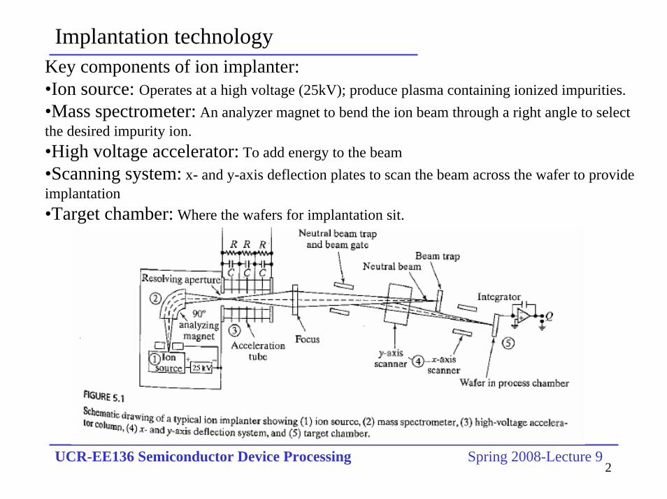
Implantation technologyKey components of ion implanter: •Ion source: Operates at a high voltage (25kV); produce plasma containing ionized impurities.•Mass spectrometer: An analyzer magnet to bend the ion beam through a right angle to select the desired impurity ion.•High voltage accelerator: To add energy to the beam•Scanning system: x- and y-axis deflection plates to scan the beam across the wafer to provide implantation•Target chamber: Where the wafers for implantation sit.
3UCR-EE136 Semiconductor Device Processing Spring 2008-Lecture 9
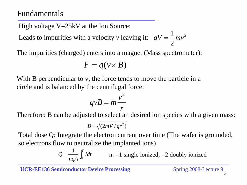
FundamentalsHigh voltage V=25kV at the Ion Source:
2
21 mvqV =Leads to impurities with a velocity v leaving it:
The impurities (charged) enters into a magnet (Mass spectrometer):
)( BvqF ×=With B perpendicular to v, the force tends to move the particle in a circle and is balanced by the centrifugal force:
rvmqvB
2
=Therefore: B can be adjusted to select an desired ion species with a given mass:
)/2( 2qrmVB =
Total dose Q: Integrate the electron current over time (The wafer is grounded, so electrons flow to neutralize the implanted ions)
∫=T
IdtnqA
Q0
1n: =1 single ionized; =2 doubly ionized

4UCR-EE136 Semiconductor Device Processing Spring 2008-Lecture 9
Meaning of dose and concentration
5UCR-EE136 Semiconductor Device Processing Spring 2008-Lecture 9
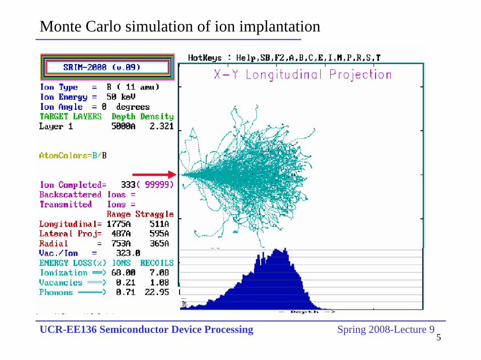
Monte Carlo simulation of ion implantation
6UCR-EE136 Semiconductor Device Processing Spring 2008-Lecture 9
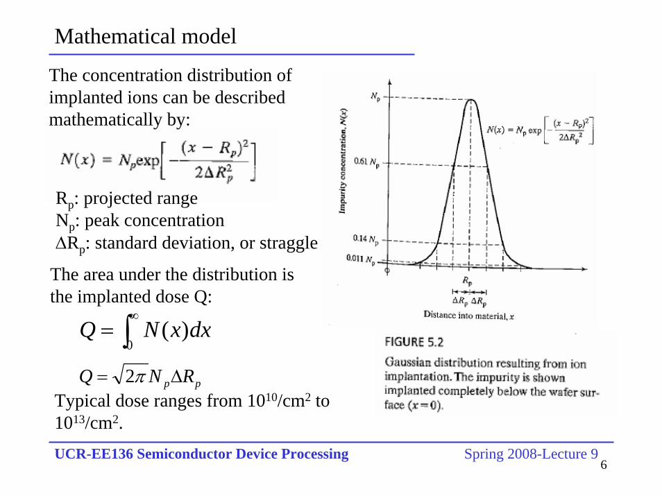
Mathematical model
The concentration distribution of implanted ions can be described mathematically by:
Rp: projected rangeNp: peak concentration∆Rp: standard deviation, or straggle
The area under the distribution is the implanted dose Q:
∫∞
=0
)( dxxNQ
pp RNQ ∆= π2Typical dose ranges from 1010/cm2 to 1013/cm2.
7UCR-EE136 Semiconductor Device Processing Spring 2008-Lecture 9
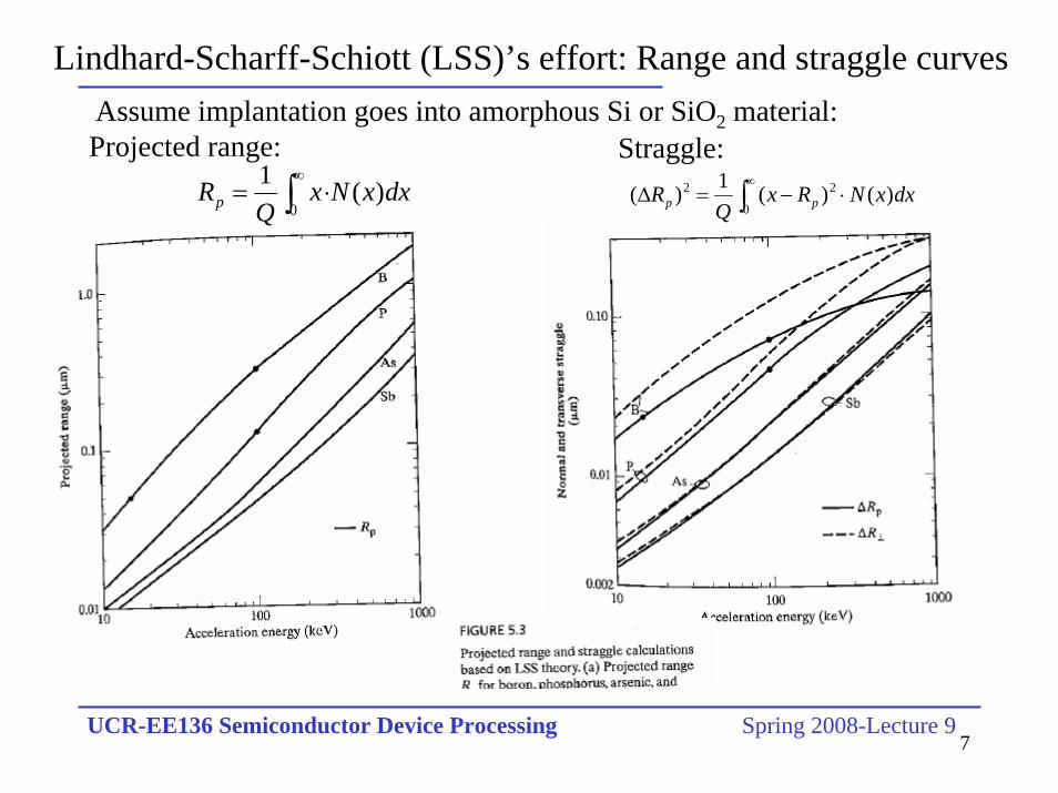
Lindhard-Scharff-Schiott (LSS)’s effort: Range and straggle curvesAssume implantation goes into amorphous Si or SiO2 material:
dxxNxQ
Rp )(10∫∞
⋅=
Projected range:
∫∞
⋅−=∆0
22 )()(1)( dxxNRxQ
R pp
Straggle:
8UCR-EE136 Semiconductor Device Processing Spring 2008-Lecture 9
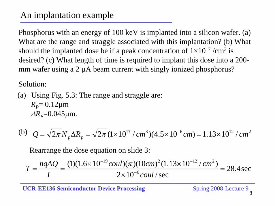
An implantation example
Phosphorus with an energy of 100 keV is implanted into a silicon wafer. (a) What are the range and straggle associated with this implantation? (b) What should the implanted dose be if a peak concentration of 1×10¹⁷ /cm3 is desired? (c) What length of time is required to implant this dose into a 200-mm wafer using a 2 µA beam current with singly ionized phosphorus?
Solution:(a) Using Fig. 5.3: The range and straggle are:
RP= 0.12µm ∆RP=0.045µm.
(b) 2126317 /1013.1)105.4)(/101(22 cmcmcmRNQ pp ×=××=∆= −ππ
Rearrange the dose equation on slide 3:
sec4.28sec/102
)/1013.1()10)()(106.1)(1(6
212219
=×
××== −
−−
coulcmcmcoul
InqAQT π
9UCR-EE136 Semiconductor Device Processing Spring 2008-Lecture 9
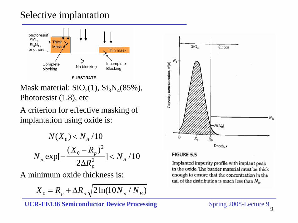
Selective implantation
Mask material: SiO2(1), Si3N4(85%), Photoresist (1.8), etcA criterion for effective masking of implantation using oxide is:
10/)( 0 BNXN <
10/]2
)(exp[ 2
20
Bp
pp N
RRX
N <∆
−−
)/10ln(20 Bppp NNRRX ∆+=
A minimum oxide thickness is:

10UCR-EE136 Semiconductor Device Processing Spring 2008-Lecture 9
Dopant depth with ion energy
•Higher ion energy (implanter acceleration voltage), greater depth•Deviation from Gaussian: light boron ions easily backscattered by Si
11UCR-EE136 Semiconductor Device Processing Spring 2008-Lecture 9
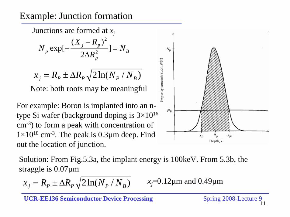
Example: Junction formation
Bp
pjp N
RRX
N =∆
−− ]
2)(
exp[ 2
2
)/ln(2 BPPPj NNRRx ∆±=
Junctions are formed at xj
Note: both roots may be meaningful
For example: Boron is implanted into an n-type Si wafer (background doping is 3×10¹⁶
cm-3) to form a peak with concentration of 1×1018 cm-3. The peak is 0.3µm deep. Find out the location of junction.
Solution: From Fig.5.3a, the implant energy is 100keV. From 5.3b, the straggle is 0.07µm
xj=0.12µm and 0.49µm)/ln(2 BPPPj NNRRx ∆±=
12UCR-EE136 Semiconductor Device Processing Spring 2008-Lecture 9
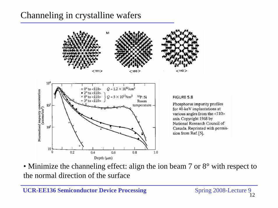
Channeling in crystalline wafers
• Minimize the channeling effect: align the ion beam 7 or 8° with respect to the normal direction of the surface
13UCR-EE136 Semiconductor Device Processing Spring 2008-Lecture 9
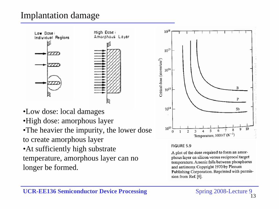
Implantation damage
•Low dose: local damages•High dose: amorphous layer•The heavier the impurity, the lower dose to create amorphous layer•At sufficiently high substrate temperature, amorphous layer can no longer be formed.

14UCR-EE136 Semiconductor Device Processing Spring 2008-Lecture 9
Dopant activation
•Implanted impurities appear interstitials•Dopant activation means moving these interstitial impurities into Si sites•Only substitutional dopants provide carriers, therefore dopants staying as interstitials are called not activated•Heat is provided to activate dopant impurities, normally at 800-900°C for 30 minutes.•The lattice damage can also be healed by heating, i.e., amorphous layer re-crystallization is possible.

15UCR-EE136 Semiconductor Device Processing Spring 2008-Lecture 9
Rapid thermal annealing (RTA) for dopant activation and re-crystallization
16UCR-EE136 Semiconductor Device Processing Spring 2008-Lecture 9
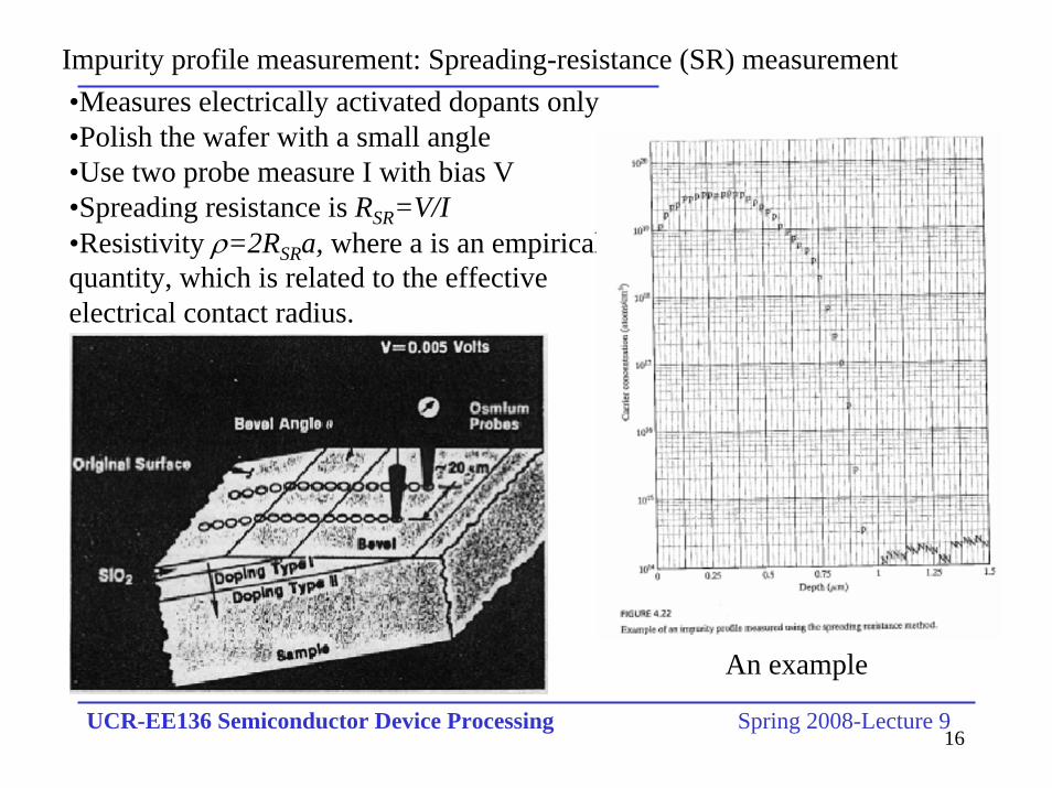
Impurity profile measurement: Spreading-resistance (SR) measurement•Measures electrically activated dopants only•Polish the wafer with a small angle•Use two probe measure I with bias V•Spreading resistance is RSR=V/I•Resistivity ρ=2RSRa, where a is an empirical quantity, which is related to the effective electrical contact radius.
An example
17UCR-EE136 Semiconductor Device Processing Spring 2008-Lecture 9
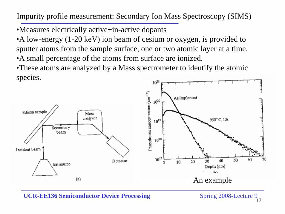
Impurity profile measurement: Secondary Ion Mass Spectroscopy (SIMS)
•Measures electrically active+in-active dopants•A low-energy (1-20 keV) ion beam of cesium or oxygen, is provided to sputter atoms from the sample surface, one or two atomic layer at a time.•A small percentage of the atoms from surface are ionized.•These atoms are analyzed by a Mass spectrometer to identify the atomic species.
An example
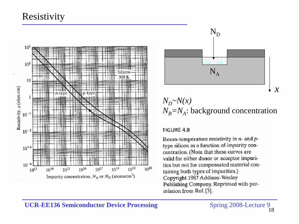
18UCR-EE136 Semiconductor Device Processing Spring 2008-Lecture 9
Resistivity
NA
ND
xND~N(x)NB=NA: background concentration

19UCR-EE136 Semiconductor Device Processing Spring 2008-Lecture 9
Sheet resistance
Rs=ρ/t is called the sheet resistance of the layer of materialNote: Rs has a unit of ohms, historically is given the special descriptive unit of ohms per square.More general (mathematical) definition:
∫==
tdxx
t 0)(1
11
σσρ
∫== ts
dxxtR
0)(
1
σ
ρ
∫ −= t
B
sdxNxNq
R0
))((
1
µ
N(x)>>NB
Constant µQqdxxNq
R ts µµ
1
)(
1
0
==∫
•Q is the total implanted dose•Use µ for peak dopant density where carries most of current

20UCR-EE136 Semiconductor Device Processing Spring 2008-Lecture 9
Four-point probe
Always almost s>>t:
1 2 3 4
I enters the film with thickness t from probe 1, spreads like a circle with radius r:
IVt /)2ln/(πρ = IVIVtRs /5324.4/)2ln/(/ === πρ
rtIj π2/=
Electrical filed from Ohm’s law: rtIjjE πρρσ 2// === drdVE /−=
V23 due to I from probe 1: ∫ ∫ ==−s
s
s
s tIdr
dtIEdr
2
22ln
22 πρ
πρ
V23 due to I leaving from probe 4: 2ln2 tIπρ The total V23 is sum: 2ln
tIVπρ
=
Current density along the radius direction is:
A demanding practice if interested: What and how you obtain for s<<t?
21UCR-EE136 Semiconductor Device Processing Spring 2008-Lecture 9
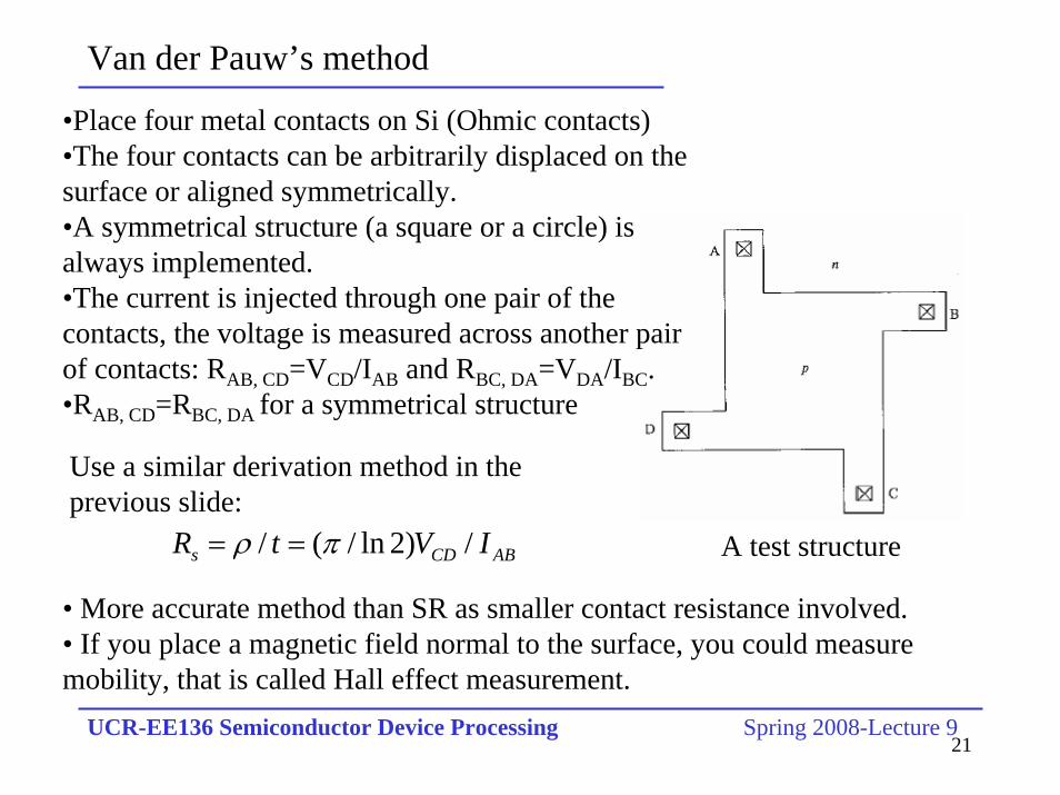
Van der Pauw’s method
•Place four metal contacts on Si (Ohmic contacts)•The four contacts can be arbitrarily displaced on the surface or aligned symmetrically. •A symmetrical structure (a square or a circle) is always implemented.•The current is injected through one pair of the contacts, the voltage is measured across another pair of contacts: RAB, CD=VCD/IAB and RBC, DA=VDA/IBC.•RAB, CD=RBC, DA for a symmetrical structure
Use a similar derivation method in the previous slide:
ABCDs IVtR /)2ln/(/ πρ == A test structure
• More accurate method than SR as smaller contact resistance involved.• If you place a magnetic field normal to the surface, you could measure mobility, that is called Hall effect measurement.