ion-shading effects during metal etch in plasma …ffchen/publs/chen221.pdfion-shading effects...
TRANSCRIPT

1388 IEEE TRANSACTIONS ON PLASMA SCIENCE, VOL. 35, NO. 5, OCTOBER 2007
Ion-Shading Effects During Metal Etchin Plasma Processing
Tsitsi G. Madziwa-Nussinov, Member, IEEE, Donald Arnush, and Francis F. Chen, Life Fellow, IEEE
Abstract—Self-consistent computations of electric fields(E-fields) and ion orbits inside trenches were done in orderto verify Hashimoto’s hypothesis of damage that is inducedduring plasma processing. In his well-accepted theory, Hashimotoproposed a mechanism for electron-shading damage, wherebythe photoresist at the tops of trenches and vias collects a negativecharge from the thermal electrons, creating an E-field, whichprevents electrons from reaching the trench bottom, wherecollector is located. The sheath E-field accelerates the ions anddrives them straight into the trench where they impinge on thecollector, and charge it positive if it is isolated. In the computationspresented in this paper, it is shown that ion orbits depend onlyon the E-fields at the entrance and are sensitive to changes in theshape of the photoresist layer there. In addition to the electron-shading mechanism, there is an “ion-shading” effect that protectspart of the trench walls, and the number of ions that strike thewall is too small to cause any deformation of the walls.
Index Terms—Electron-shading damage, ion shading, ion tra-jectories, metal etch, plasma processing.
I. INTRODUCTION
P LASMA etching [1]–[5] is currently widely used inthe fabrication of silicon-based integrated circuits. The
process is used to produce high-resolution patterns in many ofthe thin layers of the circuits and to selectively remove maskinglayers; it is based on the following sequence of microscopic re-action steps. Electrons are accelerated by dc, RF, or microwaveelectric fields (E-fields) and collide inelastically with suitableprecursor molecules to produce ions, atoms, and radicals. Acomplex mixture of reactive species is produced. Neutral andionic reactive species strike the surfaces that are in contact withthem to form products that are volatile.
In high density plasma processing, consequences ofplasma–surface interactions are to a significant extent con-trolled by the incident ion fluxes and their energies. Anelectron-free space-charge region designated as a “sheath”forms between a plasma and a contacting solid surface. Sheaths[2], [6] are of critical importance for plasma etching, sincepositive ions are accelerated toward the surface when entering
Manuscript received February 15, 2007; revised July 12, 2007.T. G. Madziwa-Nussinov is with the Los Alamos National Laboratory, Los
Alamos, NM 87545 USA (e-mail: [email protected]).D. Arnush, deceased, was with the Electrical Engineering Department,
University of California, Los Angeles, CA 90095 USA.F. F. Chen is with the Electrical Engineering Department, University of
California, Los Angeles, CA 90095 USA (e-mail: [email protected]).Color versions of one or more of the figures in this paper are available online
at http://ieeexplore.ieee.org.Digital Object Identifier 10.1109/TPS.2007.905203
Fig. 1. Illustration of electron shading. The proximity of the plasma’s sheathedge is greatly exaggerated.
a sheath. Most of the ion energy is provided by accelerationin the sheath E-fields established by self-biasing the waferchuck. The accelerated ions bombard the surface with energiesthat are much greater than thermal energies. Fabrication ofhigh-speed semiconductor circuits depends on etching submi-crometer trenches and holes with straight walls, which areguided by sheath-accelerated ions that strike the substrate at anormal angle.
The phenomenon of electron shading, as hypothesized byHashimoto [7], [8], is illustrated in Fig. 1. The electron-shadingeffect [9]–[11] is caused by the difference in isotropy of ionsand electrons. Electrons enter the sheath with an isotropic angu-lar distribution, while ions, on the other hand, are accelerated inthe presheath to the Bohm velocity. Ion velocity in the directionperpendicular to the wafer is larger than the thermal velocityof the ions in the parallel direction. This initial directionaldifference is greatly amplified as the particles traverse acrossthe sheath. Ions are accelerated, further reaching energies oftens of volts or more. The bombardment of the trench bottomloosens the first few monolayers, allowing the etchant atomsto combine much more effectively than without the ions. Atthe same time, the electrons, which remain in an isotropicMaxwellian distribution, get decelerated in the sheath, and mostof them are returned to the plasma.
Only a small fraction of the electrons crossing the sheathedge will make it to the wafer surface where they charge thenonconductive photoresist to its floating potential. This nega-tive charge allows very few electrons to enter the trench; thus,the ions deposit a positive charge onto the trench bottom [12].
A description of the model, including the assumptions madefor simplicity, is given in Section II. In Section III, some ofthe results are given and discussed. The conclusion is givenin Section IV. The bulk of the computational results is givenelsewhere [13], [14].
0093-3813/$25.00 © 2007 IEEE
MADZIWA-NUSSINOV et al.: ION-SHADING EFFECTS DURING METAL ETCH IN PLASMA PROCESSING 1389
II. MODEL
A. Model Assumptions and Scale Invariance
In plasma processing, a planar sheath separates the plasmafrom the silicon wafer onto which submicrometer circuits arebuilt by deposition and etching. These features have a minimumsize (or critical dimension) of 60 nm or below. The sheaththickness s is at least 5λD, where λD is the Debye length,and can be several times larger if a large negative dc bias isapplied to the wafer. Taking n = 1012 cm−3 and KTe = 1 eVas extreme values that are likely to exist at the sheath edge, it isfound that s is, at least, 37 µm, extending over the 200–300-mmdiameter of the wafer. Thus, the sheath is at least 100 timesthicker than the feature sizes and orders of magnitude wider. Itcan therefore be assumed that ions emitted from the sheath edgehave straight trajectories normal to the wafer as they approachits surface. As the trenches are much smaller than both thesheath and the Debye lengths, scale invariance justifies theuse of the simpler Laplace equation, rather than the Poissonequation, to compute particle trajectories in the model.
To show this justification, we write Poisson’s equation as
ε0�
∇2
V = e(�ne − �
n i). (1)
A system is adopted whereby the capped quantities (such as�
∇)are in dimensional units and the normal letters are dimension-less. With the usual definitions
η ≡ e�
V /KTe, λ2D ≡ ε0KTe/n0e
2, c2s ≡ KTe/M (2)
(1) becomes
ε0KTe
n0e2
�
∇2
η = λ2D
�
∇2
η =(ne
n0− ni
n0
). (3)
Let w be the scale length of the gradient�
∇, and define
r ≡�r /w, so that ∇2 = w2
�
∇2
. This yields
∇2η =w2
λ2D
(ne
n0− ni
n0
)≈ 0. (4)
Although ni � ne in the trench, ni/n0 is still < 1. Thus, aslong asw2/λ2
D � 1, only the dimensionless Laplace’s equation
∇2η = 0 (5)
needs to be solved, which is subject to the boundary conditionη = ηb(rb) at r = rb. The solution would be the same as that of
the dimensional problem�
∇2
η = 0 with the boundary conditionη = ηb(
�rb) at
�r=
�rb. Thus, only the aspect ratio of the trench
matters, and not its absolute size, if the Debye length λD is� w. The space charge deep inside the sheath is negligible.
The ion trajectories are computed from
d2�r
dt2= − e
M
�
∇V = − e
M
KTe
e∇η = −c2s
�
∇η. (6)
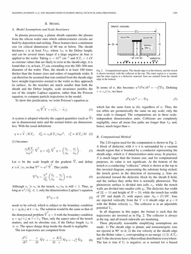
Fig. 2. Computational region. The sheath edge is at the bottom, and the trenchis shown inverted, with the collector at the top. The outer region is a vacuum,and the inner region is a dielectric material. Ions are emitted from the sheathedge at the bottom.
In terms of r, this becomes w2d2r/dt2 = −c2s∇η. Definingτ ≡ cst/w, we have
d2r/dτ2 = −∇η (7)
which has the same form as (6), regardless of w. Thus, theion orbits are geometrically the same on any scale; only thetime scale is changed. The computations are in these scale-independent dimensionless units. Collisions are completelynegligible, since all mean free paths are longer than λD and,hence, much larger than s.
B. Computational Method
The 2-D region used for the computation is shown in Fig. 2.A block of dielectric with k ≈ 4 is surrounded by a vacuumsheath region that is bounded by a conductor representing thesheath edge, which is S dimensionless units away. In practice,S is much larger than the feature size, and for computationalpurposes, its value is not significant. At the bottom of thetrench is a conducting “collector,” which is shown at the top inthis inverted diagram, representing the substrate being etched;the trench grows in the direction of increasing y. Ions areaccelerated toward the dielectric block by the sheath E-field,and the surface they strike first is normally photoresist. Thephotoresist surface is divided into cells xj , while the trenchwalls are divided into smaller cells yj . The dielectric has widthof 2L = 14 and height of H = 10, while the trench has widthof 2W and depth D, with aspect ratio AR = D/2W . Ionsare injected vertically from the V ≡ 0 sheath edge at y = 0with the Bohm velocity cs. The collector is at an adjustablepotential Vc.
In all diagrams in this paper, the format is such that thetrajectories are inverted as in Fig. 2. The collector is alwaysat the top, and all trench sidewalls are insulating.
Three physically reasonable simplifying assumptions aremade: 1) The sheath edge is planar, and monoenergetic ionsare ejected at 90◦ to it; 2) the ion velocity at the sheath edgehas the Bohm value cs corresponding to an energy (1/2) KTe;and 3) the electrons have a Maxwellian distribution everywhere.The last is true if Vc is negative, as is normal for a biased
1390 IEEE TRANSACTIONS ON PLASMA SCIENCE, VOL. 35, NO. 5, OCTOBER 2007
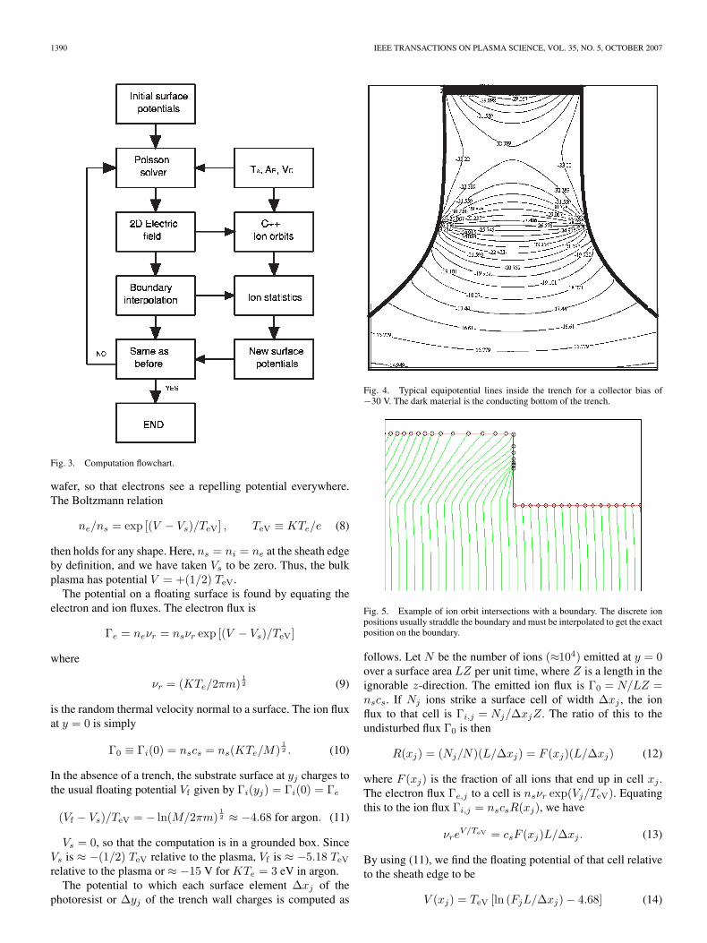
Fig. 3. Computation flowchart.
wafer, so that electrons see a repelling potential everywhere.The Boltzmann relation
ne/ns = exp [(V − Vs)/TeV] , TeV ≡ KTe/e (8)
then holds for any shape. Here, ns = ni = ne at the sheath edgeby definition, and we have taken Vs to be zero. Thus, the bulkplasma has potential V = +(1/2) TeV.
The potential on a floating surface is found by equating theelectron and ion fluxes. The electron flux is
Γe = neνr = nsνr exp [(V − Vs)/TeV]
where
νr = (KTe/2πm)12 (9)
is the random thermal velocity normal to a surface. The ion fluxat y = 0 is simply
Γ0 ≡ Γi(0) = nscs = ns(KTe/M)12 . (10)
In the absence of a trench, the substrate surface at yj charges tothe usual floating potential Vf given by Γi(yj) = Γi(0) = Γe
(Vf − Vs)/TeV = − ln(M/2πm)12 ≈ −4.68 for argon. (11)
Vs = 0, so that the computation is in a grounded box. SinceVs is ≈ −(1/2) TeV relative to the plasma, Vf is ≈ −5.18 TeV
relative to the plasma or ≈ −15 V for KTe = 3 eV in argon.The potential to which each surface element ∆xj of the
photoresist or ∆yj of the trench wall charges is computed as
Fig. 4. Typical equipotential lines inside the trench for a collector bias of−30 V. The dark material is the conducting bottom of the trench.
Fig. 5. Example of ion orbit intersections with a boundary. The discrete ionpositions usually straddle the boundary and must be interpolated to get the exactposition on the boundary.
follows. Let N be the number of ions (≈104) emitted at y = 0over a surface area LZ per unit time, where Z is a length in theignorable z-direction. The emitted ion flux is Γ0 = N/LZ =nscs. If Nj ions strike a surface cell of width ∆xj , the ionflux to that cell is Γi,j = Nj/∆xjZ. The ratio of this to theundisturbed flux Γ0 is then
R(xj) = (Nj/N)(L/∆xj) = F (xj)(L/∆xj) (12)
where F (xj) is the fraction of all ions that end up in cell xj .The electron flux Γe,j to a cell is nsνr exp(Vj/TeV). Equatingthis to the ion flux Γi,j = nscsR(xj), we have
νreV/TeV = csF (xj)L/∆xj . (13)
By using (11), we find the floating potential of that cell relativeto the sheath edge to be
V (xj) = TeV [ln (FjL/∆xj) − 4.68] (14)
MADZIWA-NUSSINOV et al.: ION-SHADING EFFECTS DURING METAL ETCH IN PLASMA PROCESSING 1391
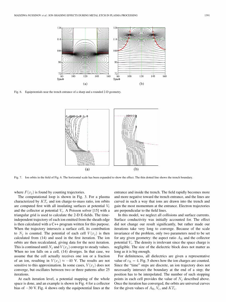
Fig. 6. Equipotentials near the trench entrance of a sharp and a rounded 2-D geometry.
Fig. 7. Ion orbits in the field of Fig. 6. The horizontal scale has been expanded to show the effect. The thin dotted line shows the trench boundary.
where F (xj) is found by counting trajectories.The computational loop is shown in Fig. 3. For a plasma
characterized by KTe and ion charge-to-mass ratio, ion orbitsare computed first with all insulating surfaces at potential Vf
and the collector at potential Vc. A Poisson solver [15] with atriangular grid is used to calculate the 2-D E-fields. The time-independent trajectory of each ion emitted from the sheath edgeis then calculated with a C++ program written for this purpose.When the trajectory intersects a surface cell, its contributionto Nj is counted. The potential of each cell V (xj) is thencalculated from (14) and used in the first iteration. The ionorbits are then recalculated, giving data for the next iteration.This is continued untilNj and V (xj) converge to steady values.When no ion falls on a cell, (14) diverges. In that case, weassume that the cell actually receives one ion or a fractionof an ion, resulting in V (xj) ≈ −40 V. The results are notsensitive to this approximation. In some cases, V (xj) does notconverge, but oscillates between two or three patterns after 25iterations.
At each iteration level, a potential mapping of the wholespace is done, and an example is shown in Fig. 4 for a collectorbias of −30 V. Fig. 4 shows only the equipotential lines at the
entrance and inside the trench. The field rapidly becomes moreand more negative toward the trench entrance, and the lines arecurved in such a way that ions are drawn into the trench andgain the most momentum at the entrance. Electron trajectoriesare perpendicular to the field lines.
In this model, we neglect all collisions and surface currents.Surface conductivity was initially accounted for. The effectdid not change our result significantly, but rather made ouriterations take very long to converge. Because of the scaleinvariance of the problem, only two parameters need to be setfor any given geometry: the aspect ratio AR and the collectorpotential Vc. The density is irrelevant since the space charge isnegligible. The size of the dielectric block does not matter aslong as it is big enough.
For definiteness, all dielectrics are given a representativevalue of εR = 4. Fig. 5 shows how the ion charges are counted.Since the “time” steps are discrete, an ion trajectory does notnecessarily intersect the boundary at the end of a step; theposition has to be interpolated. The number of such stoppingpoints in each cell provides the value of Nj described above.Once the iteration has converged, the orbits are universal curvesfor the given values of AR, Vc, and KTe.

1392 IEEE TRANSACTIONS ON PLASMA SCIENCE, VOL. 35, NO. 5, OCTOBER 2007
Fig. 8. Ion-shading effect for AR = 5 and Vc = −26 V (left), AR = 7 and Vc = −26 V (center), and AR = 7 and Vc = −40 V (right). The horizontal scalehas been expanded.
Fig. 9. Ion collection regions in trenches with AR = 7, 5, and 3, with Vc =−26 V. The light regions of the trench wall are not struck by any ions.
III. RESULTS
A. Ion Shading
Fig. 6 shows typical E-field patterns near the trench entrancesthat are sharp and curved. Trench boundaries are superimposedon the figures. Because of the sharp corners in Fig. 6(a), the fieldis extremely strong there and causes a large deflection of theions, as shown in Fig. 7(a). To suppress this unphysical effect,the corners were subsequently rounded into a circular arc. Theresulting trajectories [Fig. 7(b)] are more reasonable, but thefact remains that no or very few ions can strike the sidewallnear the entrance. This ion shadowing effect, which occurs inaddition to the well-known electron-shading effect, is caused bythe E-fields outside the trench, which curve the orbits inward.At large negative collector potentials, the entire sidewall canbe protected from ion bombardment, as shown in Fig. 8. Thedecrease in sidewall ions, as the collector potential is increased,was found to be more or less exponential. Physically, the ionsgain enough energy at large |Vc| that the negative sidewallscannot deflect them.
That ion shading increases with AR is a more subtle effect.The shaded region along the sidewalls in Fig. 9 shows wherethe ions fall for three values of AR at constant Vc. The reasonthat ions are deflected into the sidewalls only for low AR canbe seen from the self-consistent field patterns in Fig. 10. It is
seen that the fields are very strong at the ends of the trench,particularly at the corners. At AR = 7, the interior of the trenchis essentially field-free. Ions are deflected into the sidewall onlyin the arc region. At AR = 3, the fields extend into the interior,where Ex is large enough to impart transverse momentum tothe ions streaking in the y-direction.
B. Nature of the Ion Trajectories
The quantitative results can be better understood if one firstobserves the nature of the ion orbits. Fig. 11 shows three viewsof the trajectories at AR = 5 and Vc = −26 V. Fig. 11(a) showsthe orbits on a normal x−y scale. The ions enter the trenchat high velocity, and their deflections are so small that theycannot be seen on this scale. In Fig. 11(b), the horizontal scalehas been expanded by a factor of 20. Here, it can be seenthat the ions enter the trench at an angle due to the externalE-field. No ions strike the first part of the wall, which isshaded. The negative charges on the wall eventually deflectthe ions outward, causing them to strike the corner of thetrench. In Fig. 11(c), the horizontal scale has been stretchedby a factor of 80, and intermediate orbits have been plotted,which are shown by the thin lines. Orbits that pass near thecorner of the photoresist actually cross and take shapes thatare sensitive to the strong fields at the entrance corner. Notethat the corner is actually circular, but looks sharp only on this80-to-1 scale. The pulling of ions into the trench by the chargeon the photoresist is shown more clearly in Fig. 12. Incidentions (indicated by the solid lines), headed for the photoresistsurface outside the trench, are drawn into the trench by the fieldsin the arc region. The trajectories show that the ions are bentaway from the corner of the photoresist instead of toward it.In the first iteration of the computation, ions land in the corner.The ions landing there then change the surface charge. The self-consistent surface charge then bends the trajectories the waythey are shown, consistently with the equipotential curves inFigs. 4, 6, and 10).
C. Effect of Photoresist Shape
As etching progresses, the photoresist will change its shape atthe trench entrance, and this will affect the ion orbits. Since theE-fields are strongest there, we expect that the ion orbits wouldbe sensitive to these changes. First, consider the change from

MADZIWA-NUSSINOV et al.: ION-SHADING EFFECTS DURING METAL ETCH IN PLASMA PROCESSING 1393
Fig. 10. Field patterns (equipotentials) for AR = 7 (left) and AR = 3 (right), at Vc = −22 V.
Fig. 11. Ion orbits for AR = 5 and |Vc| = 26 V with the horizontal scale (a) normal, (b) expanded by a factor of 20, and (c) expanded by a factor of 80 relativeto the vertical scale. The orbit spacing has been decreased near the wall for clarity.
Fig. 12. Ion orbits near the trench edge for AR = 7 and Vc = 22.
a mathematically sharp edge to the rounded edge used in ourcalculations. This was originally done to improve the conver-gence of the iterations, but the change in orbits was significant.
TABLE IION DISTRIBUTIONS WITH SHARP AND ROUNDED CORNERS
Table I shows the percentage of ions landing on each part ofthe trench for a sample of about 104 ions emitted from theentire sheath area. On the photoresist surface, including the arcregion, the potential is solved self-consistently, as it was on thetrench walls.
Table I also shows that fewer ions reach the collector if thecorner is sharp rather than rounded. This is because the sharp

1394 IEEE TRANSACTIONS ON PLASMA SCIENCE, VOL. 35, NO. 5, OCTOBER 2007
Fig. 13. Distribution of ion collection for sharp and rounded trench entrances. The ion statistics for these figures are shown in Table I.
Fig. 14. Profiles of trench entrances without and with bumps.
TABLE IIION DISTRIBUTIONS WITH SMALL BUMPS
corner more effectively shields ions approaching the trench atan angle. In either case, the fraction of ions hitting the sidewallis extremely small and cannot cause the trench profile defectsthat have been observed. As expected, the collector currentincreases, and sidewall current decreases at the higher |Vc| of26 V. The difference between cases A and B is even morenoticeable in the distribution of ions shown in Fig. 13. In caseA, ions are collected over a large part of the sidewall, while incase B, ions are shielded from all but the last bin.
To see the effect of small changes to the entrance shape, smallbumps were added onto the arc region in two locations. Thestatistics are shown in Table II for a sample of 50 000 ions.In case III, the bump is farther from the trench than incase II, as shown in Fig. 14. The sidewall ion distributionsare shown in the histograms in Fig. 15. It is clear that evena small deformation of the photoresist will change the ion
orbits drastically. The self-consistent equipotential lines forthese three cases are shown in Fig. 16. In case I, the E-fieldis very strong near the entrance. The ions are given a kick thereand then coast to the trench bottom (at the top in the figure)through the nearly field-free trench. The collector is given onlya small bias in this example, so that ions are not strongly drawninto it; some of them hit the sidewall near the bottom, givingrise to E-fields near the bottom corner. In case II, the bumpshadows part of the arc region, and the negative surface chargein the shadow gives the ions an extra kick, causing them all toland on the collector, and thus, no sidewall ions. In case III,the bump is back far enough that the ions are deflected intothe arc region, lowering the field there. Having undergoneless acceleration, the ions are drawn by transverse fields intothe sidewall. Nonetheless, the top part of the sidewall is stillshadowed. This sensitivity to the exact shape of the photoresistmeans that the ion orbits change during the etch and cannot bepredicted. Fortunately, the ion flux to the sidewalls is in everycase so small compared with that on the collector that it cannotsignificantly affect the quality of the etch.
IV. SUMMARY AND CONCLUSION
By reducing the problem to a simple dimensionlessform, universal curves were obtained for ion trajectories inetched trenches, self-consistently with the sidewall potentials.

MADZIWA-NUSSINOV et al.: ION-SHADING EFFECTS DURING METAL ETCH IN PLASMA PROCESSING 1395
Fig. 15. Sidewall ions location for cases I and III. No ions were collected on the sidewalls for II.
Fig. 16. Field patterns for the profiles shown in Fig. 14.
Reflection of ions from the walls was ignored. Results de-pend on only two parameters: the aspect ratio AR, and thepotential Vc at the trench bottom. Principal findings are asfollows.
1) E-fields that are external to the trench cause the ions toenter the trench at an angle. This causes an ion-shadingeffect, which protects the top part of the trench, andsometimes all of it, from ion bombardment.
2) Ion orbits are determined mainly by the strong fields atthe corners of the entrance; they then coast through thetrench with little additional deflection.
3) In spite of the strong fields at the entrance, ion orbits arenearly straight and vertical. Therefore, few ions strike thesidewall that they cannot cause deformations of the trenchprofile.
4) The small ion flux to the walls is very sensitive to theexact shape of the photoresist at the top. This will changein an unpredictable way during the etching process.
5) Contrary to intuition, a deep trench with large AR willhave an insignificant number of ions striking the wall.
These observations differ from commonly held conceptionsof how the ion flux behaves in reactive ion etching. By exam-ining the variation with AR, one can get an idea of the changesin ion behavior as the etch progresses. By varying Vc, one cangauge the changes during an RF cycle. However, we must notethat findings of this paper do not take into consideration theeffect of specific plasma chemistry, but are rather generalizedto any ions present in the plasma.
REFERENCES
[1] M. A. Lieberman and A. J. Lichtenberg, Principles of Plasma Dischargesand Materials Processing. New York: Wiley, 1994.
[2] G. S. Oehrlein, M. F. Doemling, B. E. E. Kastenmeier, P. J. Matsuo,N. R. Rueger, M. Schaepkens, and T. E. F. M. Standaert, “Surface scienceissues in plasma etching,” IBM J. Res. Develop., vol. 43, no. 1/2, pp. 181–198, 1999.
[3] S. M. Sze, Physics of Semiconductor Devices. New York: Wiley, 1981.[4] M. Armacost, P. D. Hoh, R. Wise, W. Yan, J. J. Brown, J. H. Keller,
G. A. Kaplita, S. D. Halle, K. P. Muller, M. D. Naeem, S. Srinivasan,H. Y. Ng, M. Gutsche, A. Gutmann, and B. Spuler, “Plasma-etchingprocesses for ULSI semiconductor circuits,” IBM J. Res. Develop.,vol. 43, no. 1/2, pp. 39–72, 1999.

1396 IEEE TRANSACTIONS ON PLASMA SCIENCE, VOL. 35, NO. 5, OCTOBER 2007
[5] T. Arikado et al., “Single silicon etching profile simulation,” Jpn. J. Appl.Phys., vol. 27, pt. 1, no. 1, pp. 95–99, Jan. 1988.
[6] F. F. Chen, Plasma Physics and Controlled Fusion. New York: Plenum,1990.
[7] K. Hashimoto, “New phenomena of charge damage in plasma etching:Heavy damage only through dense-line antenna,” Jpn. J. Appl. Phys.,vol. 32, no. 12B, pp. 6109–6113, Dec. 1993.
[8] K. Hashimoto, “Charge damage caused by electron shading effect,” Jpn.J. Appl. Phys., vol. 33, no. 10, pp. 6013–6018, Oct. 1994.
[9] N. Fujiwara, T. Maruyama, and M. Yoneda, “Profile control of poly-Si etching in electron cyclotron resonance plasma,” Jpn. J. Appl. Phys.,vol. 34, no. 4B, pp. 2095–2100, Apr. 1995.
[10] G. S. Hwang and K. P. Giapis, “On the link between electron shadowingand charging damage,” J. Vac. Sci. Technol. B, Microelectron. Process.Phenom., vol. 15, no. 5, pp. 1839–1842, Sep. 1997.
[11] K. P. Giapis and G. S. Hwang, “Pattern-dependent charging and the role ofelectron tunneling,” Jpn. J. Appl. Phys., vol. 37, no. 4B, pp. 2281–2290,Apr. 1998.
[12] R. Wise, S. Panda, S. Mathad, and R. Ranade, “Observations of pattern-dependent plasma charging and polymer deposition during deep trenchdry etch,” Future Fab Int., vol. 11, Jun. 29, 2001.
[13] T. G. Madziwa-Nussinov, “The role of ions in charging damage duringhigh density plasma etching,” M.S. thesis, UCLA, Los Angeles, CA,2003.
[14] T. G. Madziwa-Nussinov, D. Arnush, and F. F. Chen, “Ion orbits in plasmaetching of semiconductors,” Phys. Plasmas, (to be published).
[15] TriComp E-Stat 6.0, and TriComp Mesh 6.0 Codes. Copyright FieldPrecision. [Online]. Available: http://www.fieldp.com
Tsitsi G. Madziwa-Nussinov (M’99) was born inZimbabwe. She received the B.Sc. Hons. degree inphysics from the University of Zimbabwe, Harare,Zimbabwe, in 1994 and the M.S. degree in physicsand the Ph.D. degree in electrical engineering fromthe University of California, Los Angeles, in 1997and 2003, respectively.
Since 2005, she has been with the Plasma Physicsgroup at Los Alamos National Laboratory, LosAlamos, NM, doing experiments on the reconnectionscaling experiment, where she is currently a Postdoc-
toral Fellow working on plasma thruster experiments.
Donald Arnush, was a Group Leader with TRW Inc., Redondo Beach, CA, formany years. After retirement, until his death, he was an Adjunct Professor withthe Electrical Engineering Department, University of California, Los Angeles.
Francis F. Chen (SM’72–LF’80) received the Ph.D.degree from Harvard University, Cambridge, MA,in 1954.
He is a Plasma Physicist with a career extendingover 52 years and encompassing both experimentand theory. He has devoted about a decade eachto the subfields of magnetic fusion, laser fusion,plasma diagnostics, basic plasma physics, and low-temperature plasma physics. He is the author of thetextbook Introduction to Plasma Physics and Con-trolled Fusion. His current research interest includes
plasma processing of semiconductor circuits, particularly the radio-frequencysources used to make computer chips, and the physical processes that permitetching millions of transistors on a single chip. Although formally retired fromteaching, he still maintains an Active Research Group, Electrical EngineeringDepartment, University of California, Los Angeles.