ipvea update issue 7
DESCRIPTION
Members’ news of deals, partnerships, equipment sales and installations; PV trade associations lobby EU on proposed changes that could harm business; Spain intends to limit hours of PV plants, reduce feed-in tariffs; New products from Schiller Automation, Komax, Laytec , Rena, E+H, Vitronic; Latest processes and advancements in various aspects of PV production; Logistics in the Solar Supply Chain by DB SchenkerEuPD FOCUS ON GREAT BRITAIN Exclusive Q&A with Markus A.W. Hoehner & Markus Monssen-Wackerbeck; Targray’s Andrew Richardson and ROFIN’s Richard Hendel; VLSI forecasts 2010 to be boom year for suppliers of PV; WHITE PAPERS In-depth technical reports from OTTO-CHEMIE on Sustainable Quality for Long-Term Investments; ROFIN on Selective Emitters; and Peak Sun Silicon on whether the solar industry needs high purity performance chemicals; Upcoming solar trade shows around the worldTRANSCRIPT

+1 yr
SOLAr EVENTS
CALENDAr
The seeds of recovery?
White papers On Sustainable Quality, Selective Emitters and
Chemical Purity
InterviewsIPVEA member executives
Latest technology breakthroughs
Solar supply chain logistics
EuPD Examines the UK Market
New EU laws could hamper PV development
Spain aims to limit PV plant hours, reduce feed-in tariffs
PV equipment suppliers report things looked brighter in first half of 2010
also…
InternatIonal PhotovoltaIc equIPment assocIatIon - worldwIde voIce for the Pv equIPment manufacturIng Industry
updateNo.7 - SEPTEMBER 2010
NEWS EVENTS ARTICLES WHITE PAPERS MARKET DATA JOBS PRODUCTS NEW TECHNOLOGY
EU PVSEC
SPECIAL EDITION

2 | IPvea uPdate | sePtemBer 2010
t h e w o r l d w I d e v o I c e f o r t h e P v e q u I P m e n t m a n u fa c t u r I n g I n d u s t r y
IPVEA UPDATE - SEPTEMbEr 2010
Dear Readers, welcome to our special euPvsec edition of the IPvea update. the 25th euPvsec, which is this year’s major show, brings together not only the latest in photovoltaic technology, but also the entire value chain and business opportunities.
IPvea was formed by the industry for the industry, and so the board members are anxious to receive and act upon feedback from members in particular as to which events to sponsor for next year. many of our members have requested that the shows, while continuing to focus on photovoltaic
technology and its roadmap, incorporate ways to reduce the events in the calendar year. the presence and support of IPvea members is the result of such requests and I would like to thank euPvsec for being such a stronger partner.
as the industry and its technology constantly changes, you can be sure IPvea will be there to chronicle all the machinations in nearly real time. IPvea = I know it!
I wish you a successful show!
Best regards,
Sven Jarby, PresidentInternational PV Equipment Association (IPVEA)
europe address: IPvea International Photovoltaic equipment association P.o. Box 1610, d-63406 hanau, germany
us address: IPvea International Photovoltaic equipment association P.o. Box 771507, orlando, florida 32877, usa tel: +1 407 856 9100 fax: +1 407 856 9500
managing director: Bryan ekus [email protected]
registration number: court hanau vr 31714
disclaimer: IPvea International Photovoltaic equipment association has used uses its best efforts to ensure that all the information in this publication is up-to-date. any warranty to the correctness and actuality can not be assumed. IPvea International Photovoltaic equipment association reserves the right to make changes or additions to the information made available at any time without notice.
copyright: © 2010 International Pv equipment association. all rights reserved. contents may not be reproduced by any means, in whole or part, without the prior written permission of the publisher. the opinions expressed in the IPvea newsletter are not necessarily those of the International Pv equipment association.
editor in chief: Bryan ekus [email protected]
managing editor: larry Jaffee [email protected]
design and layout: doubletake design ltd. www.doubletakedesign.co.uk
Publisher: IPvea International Photovoltaic equipment association
ContentsINDUSTrY bUZZmembers’ news of deals, partnerships, equipment sales and installations
GOVErNMENT UPDATEPv trade associations lobby eu on proposed changes that could harm business; spain intends to limit hours of Pv plants, reduce feed-in tariffs
LATEST EQUIPMENTnew products from schiller automation, Komax, laytec , rena, e+h, vitronic
NEW TECHNOLOGYlatest processes and advancements in various aspects of Pv production
FEATUrE ArTICLElogistics in the solar supply chain by dB schenker
EuPD FOCUS ON GrEAT brITAINexclusive q&a with markus a.w. hoehner & markus monssen-wackerbeck
INTErVIEWS WITH IPVEA MEMbEr EXECUTIVEStargray’s andrew richardson and rofIn’s richard hendel
INSIDE IPVEAPv Production forum 2010 Programme, IPvea members’ meeting 2010
MArKET UPDATEvlsI forecasts 2010 to be boom year for suppliers of Pv
WHITE PAPErSIn-depth technical reports from otto-chemIe on sustainable quality for long-term Investments; rofIn on selective emitters; and Peak sun silicon on whether the solar industry needs high purity performance chemicals
INDUSTrY CALENDArupcoming solar trade shows around the world

CONTENTS
hIghlIghts
sePtemBer 2010 | IPvea uPdate | 3
like to have your say? IPvea would love to hear your news or views please e-mail [email protected]
22
104
28 30
17
25th EU PVSEC IPVEA MEMbEr LOCATIONS3S Swiss Solar Systems AG L2/H2/D1
ABB S.A. L3/H2/B16
ACI-ecotec GmbH & Co. KG L3/H4/D22
AEG Power Solutions GmbH L3/H4/B1
AIS Automation Dresden GmbH L2/H3/D45
AMB Apparate + Maschinenbau GmbH L2/H2/D1
Applied Materials L2/H2/B1
Bekaert N.V. L2/H4/A52
Bosch Rexroth AG L2/H4/D9
Bürkle GmbH L2/H2/D10
centrotherm photovoltaics AG L2/H4/D13
Dek Solar L2/H4/B14
Diamond Materials Tech, Inc. L2/H2/D1
Dr. Schenk GmbH L2/H4/B10
dr. schwab Inspection Technology L2/H2/A45
E+H Metrology GmbH L2/H3/C14
Ferrotec GmbH L2/H2/A43
GfE Metalle und Materialien GmbH L2/H2/A46
Hennecke Systems GmbH L2/H2/D1
Honeywell L2/H4/C1
InnoLas Systems GmbH L2/H2/B9
ISRA SURFACE VISION GmbH L2/H3/D46
Jonas & Redmann Photovoltaics Production Solutions GmbH L2/H2/B13
KITEC microelectronic technologie GmbH L2/H2/A53
Komax Solar L2/H2/D4
KUKA Systems GmbH L2/H2/B10
LayTec GmbH L2/H2/A51
LPKF SolarQuipment GmbH L2/H4/C8
M+W Group L2/H3/B15
Manz Automation AG L2/H2/D13
Meier Solar Solutions GmbH L2/H2/A29
Meyer Burger AG L2/H2/D1
Meyer Burger Automation GmbH L2/H2/D1
Meyer Burger Technology AG L2/H2/D1
Newport Spectra-Physics GmbH L2/H4/A36
Oerlikon Leybold Vacuum GmbH L2/H2/C4
Oerlikon Solar Ltd., Trubbach L2/H2/B8
OTB Solar L2/H4/B4
Otto Chemie L2/H2/A26
Pall GmbH L2/H2/D16
Pasan SA L2/H2/D1
REIS ROBOTICS L2/H2/D11
RENA GmbH L2/H2/B5
ROFIN Baasel Lasertech L2/H4/C15
Roth & Rau AG L2/H4/B5
SCHILLER AUTOMATION GmbH & Co. KG L2/H2/C8
SEMILAB Semiconductor Physics Laboratory Co., Ltd. L2/H2/A47
Singulus Technologies AG L2/H2/B11
Soleras Ltd. L2/H2/A6
SOMONT GmbH L2/H2/D1
Spire Corporation L2/H4/B15
Stangl Semiconductor Equipment AG L2/H2/B11
Synova S.A. L2/H2/C18
Targray Technology International Inc. L2/H4/A15
teamtechnik GmbH L2/H2/C15
Tempress Systems L2/H2/B7
TRUMPF Laser- und Systemtechnik GmbH L2/H4/C4
Veeco Instruments L2/H2/A31
VITRONIC Dr.-Ing. Stein Bildverarbeitungssysteme GmbH L2/H3/C19
VON ARDENNE L2/H4/C14
PV Production Forum 2010Organized by EU PVSEC & IPVEA7 September 2010, Valencia, Spain
the Pv Production forum will be led by industry experts from manufacturers and suppliers of photovoltaic (Pv) fabrication equipment and related raw materials. It will provide an essential opportunity for networking across all segments of the Photovoltaic production industry and inform about the changing dynamics, processes and production technology steps in the Pv manufacturing supply chain.
IPVEA Members’ Meeting8th September 2010, 8:30 - 9:30amLocation: Sala Ausias March, in the Exhibition Area (entry Foro Centro), Valencia Feria, Spain
SAVE THE DATES!

4 | IPvea uPdate | sePtemBer 2010
information
IPVEA EVEnts
reis introduces cost- and quality-optimized solar module productionreis robotics presents at bOOTH D11, HALL 2, LEVEL 2, its latest advances in quality assurance and cost savings for fully automated solar module production lines. the company demonstrates how the quality of the solar modules in existing production systems can be increased at the same time as increasing productivity. By means of electro-luminescence a system will recognize faulty cells automatically, even before they are laminated.
ther company’s automatic electro-luminescence measurement of string and matrix measures the quality of strings before laying them into the matrix. the extended system allows the complete matrix to be assessed before the lamination process. faulty or damaged solar cells are detected automatically with a camera and thus can be fed out straight away. defective cells can be replaced or repaired in time and be used again immediately in the production process. the so-called electro-luminescence measurement analyses solar cells with high resolution within a few seconds.
reis will also exhibit its fully automatic direct assembly of the j-box at the Pv-module after lamination onto a photovoltaic module. connection and assembly is done for the first time after lamination of the strings in the module, giving greater safety and cost savings because some steps are omitted before lamination.
www.reisrobotics.de
dr. schwab showcases inline wafer inspectiondr. schwab Inspection technology will showcase at bOOTH A45, HALL 2, LEVEL 2 it newly developed inline wafer inspection system fPI wafer to examine texturing and sin coating layer on mono- and multicrystalline silicon wafers.
fPI wafer is equipped with our proprietary series of spectrometers and allows high-speed and high-resolution measurement to analyze the spectral reflectance of wafers within the cycle time of production. the results provide detailed information about degree and uniformity of texturing, coating thickness and colour.
the modular design of fPI wafer allows easy integration into any production line. the system combines high-precision measurement with closed loop feedback functionality, powerful data analysis and result presentation together with user-friendly operation.
www.schwabinspection.com
DEK’s Eclipse showcases production flexibility deK solar, booth b14, HALL 4, LEVEL 2 will introduce visitors to the eclipse metallization line’s unprecedented flexibility and high throughput solution for commercial solar cell production.
senior process development specialist, tom falcon, will also be presenting the company’s latest breakthroughs in Print-on-Print (PoP) technology during the show.
launching an entirely new, flexible platform design concept, eclipse incorporates a series of field retrofittable process modules that enable manufacturers to easily scale production up and down, to 1200, 2400 or 3600 wph. the primary process modules, including the print head and loader, incorporate master controls and are designated as master units. additional process modules operate as secondary “slaves,” making the scale-up process even more cost effective.
eclipse performance can be easily upgraded in the field for manufacturers who forsee a production ramp up in their future. spacer process modules equipped with conveyors can be deployed at initial installation, then simply exchanged for additional print capacity when demand dictates – eliminating the need to reconfigure the entire line to accomodate extra modules and streamlining scalability even further.
www.deksolar.com
Targray exhibits line of PV materialstargray will be exhibiting on bOOTH A15, HALL 4, LEVEL 2 its full-line of photovoltaic materials and focused solutions which enable solar cell and module manufacturers to maximize their cell and module quality and reliability, while significantly lowering their manufacturing cost per watt.
the company works with several global partners to bring to market materials including Polysilicon, solar wafers and cells, Broken solar cells, silver Paste, aluminum Paste, sputtering targets, silicone sealants, adhesives and Potting agents, tabbing
SHOW PREViEW EU PVSEC SEPtEmbER 2010

sePtemBer 2010 | IPvea uPdate | 5
information
event uPdates
ribbon, encapsulant, Junction boxes and more.
targray is a global company with operations and customers in more than 50 countries throughout asia, europe and the a mericas.
www.targray.com
rexroth reduces costs, complexity Visit HALL 4, LEVEL 2, bOOTH D09 to find out about rexroth’s expansion of its extensive automation kit for the Pv industry. It covers all drive and control technologies for the entire production process from the ingot production to metallization, stringing, lay-up and flashing. In this connection, the kit enters new dimensions for increasing productivity with low production costs.
the new vertical transfer for the tssolar assembly system bridges level differences from several hundred millimeters to several meters. together with camolIne, the cartesian motion Building system with positive-locking connection technology, rexroth opens up the possibility to replace the robots that have been used until now by cartesian systems with considerably increased efficiency.
using the control technology that can be finely scaled in hardware and software, rexroth considerably reduces complexity and allows for far-reaching standardization.
www.boschrexroth.com
Singulus to exhibit broad range of machines, solutionssingulus technologies will be exhibiting its solutions for front-end technology for the production of crystalline silicon solar cells at bOOTH b11, HALL H2. singulus will offer a broad product range of new machines for the photovoltaics industry,
with new production technologies and therefore particular cost advantages for manufacturers of silicon cells. singulus entered strategic partnerships to offer front-end technology for the production of silicon solar cells as a one-stop supplier as well as complete, integrated production systems. such complete systems cover all individual production steps from the first cleaning process of the wafer to the finished cell.
with solare, singulus offers a production system available as batch as well as inline concept, especially reducing the cost per cell following the cost pressures in the photovoltaics market. solare provides a 30 mw or a 60 mw capacity of crystalline silicon cells.
at eu Pvsec, the company will also present the singular Pecvd tool for crystalline silicon solar cell production. singular is a coating tool for the application of anti-reflection coatings (arc) on crystalline silicon solar cells.
with stangl’s vitrum system, singulus is presenting a machine which can process thin film solar glass substrates with lengths between 1,200 and 2,600 mm, and a width range of 600 to 2,200 mm.
www.singulus.de
VITrONIC scans for optimized cell inspectionvItronIc presents its newly developed color line scan camera system of the product line vInsPecsolar at bOOTH C19, HALL 3 at eu Pvsec.
the system solution combines color and print inspec-tions of cell front sides with a an unmatched to this moment.
the heart of vItronIc’s new vInsPecsolar system is a high-resolution color line scan camera which pro-vides 64 mPixel of image
information. this is possible through four individual lines for the color ranges red, green, blue as well as black and white, which each have a resolution of 40 µm. together with the optimal led illumination, excellent print quality and color classification are guaranteed.
color, surfaces, edges and geometries are precisely and reliably inspected.
the system also promises faster micro-crack detection, improved process monitoring in the texture inspection and an even higher resolution in the print inspection.
www.vitronic.de
E+H to display its high precision metrologyAt bOOTH 14, HALL 3, LEVEL 2, e+h metrology will be exhibiting its range of metrology tools for measuring thickness, resistivity, bow, waviness, saw marks and P/n.
the product range starts with simtools on show, ple manual or embedded systems and scales up to fully automated metrology systems.
the company’s metrology specialities include: geometry, stress, thickness, resistivity, warp, waviness and roughness.
since 1968, e+h metrology has supplied a wide range of high precision, high speed and reliable metrology tools for semiconductor “in process” applications and r&d.
e+h metrology has been supporting the first Pv applications since the early 1990s and has a reputation for highly repeatable measurement results.
www.eh-metrology.com

nEWS
Industry BuZZ
6 | IPvea uPdate | sePtemBer 2010
Meyer burger lands new Asian contracts meyer Burger technology ltd. has concluded a contract for wire saws and wafer inspection systems for approximately chf 20 million with Jiangxi sornid hi-tech co., ltd., Jiujiang, china.
In the course of Jiangxi sornids’ planned expansion of production capacity up to 500mw in 2010, the slicing systems of meyer Burger ltd and the wafer inspection systems of hennecke systems gmbh will secure the manufacturing of high-grade quality multi-crystalline solar wafers.
meyer Burger and its group member hennecke systems gmbh landed the contracts for the supply of high-tech wiresaws and wafer inspection systems.
Jiangxi sornid hi-tech co., ltd was established in 2008. It is one of the largest Pv corporations in Jiangxi province, and is dedicated to grow into one of china’s most influential new energy companies.
“we are committed to becoming a leading supplier of high quality multi-crystalline silicon wafers to the solar industry,” said luo hong, chairman.
www.sornid.comwww.meyerburger.ch
Cattle-barn powered with 3S solar modulessince the end of april, 1,758 megaslate solar modules from 3s swiss solar systems, a subsidiary of meyer Burger technology ag, have been producing electricity from the power of the sun on the roof of a cattle-barn in switzerland.
the trend-setting project in melchnau, close to langenthal in the canton of Bern, com-bines technological progress in solar power with the agricultural tradition of living in harmony with nature.
93,000 kwh of electricity have already been produced on a surface area of 1,885 m2 on the roof the barn.
with an installed output of 264 kwp, the fa-cility generates about 250,000 kwh of solar power and thus supplies approximately 65 households. the new construction of the agricultural building in melchnau was fitted with a Pv installation on the roof surface, which is directed towards the south.
as the biggest consumer of the electricity produced, the swiss telecommunications company swisscom is also supporting the project which can be financed without the swiss government’s cost-covering energy supply credit.
www.3-s.ch
LayTec names two new Asian distribution partners laytec announced that it recently expanded its distribution network in asia for its in-line metrology systems.
In Korea laytec will work with dKsh Korea ltd., of seoul. as a provider of market expansion services, dKsh offers a broad portfolio of technical and service solutions.
In taiwan mos technology Inc. will repre-sent laytec. the company was founded in 1997 and is located in Zhubei city, hsinchu county. mos technology Inc. offers solu-tions and comprehensive after-sales service.
laytec separately announced that it ex-panded its headquarters in Berlin this year by 800 sq.m. and its staff has grown to 60 employees. the company is also looking to hire experimental physicists specializing in Pv and a manager for business develop-ment manager for Pv.
www.laytec.dewww.dksh.kr www.mostec.com.tw
DEK Solar makes key executive hiredeK solar has announced the appointment of steve fuszard as its new Production team leader. the move is part of the divi-sion’s drive to fully integrate the build of its metallization platforms into the successful lean manufacturing Build Programme now proven throughout the deK organisation.
having already dramatically reduced Pv industry lead times worldwide, the next phase of this initiative looks set to yield even faster equipment turnaround times for deK solar customers. In his new role, steve will be charged with developing the build processes of the company’s award-winning PvP1200 photovoltaic metallization plat-form to incorporate the organisation’s com-mitment to lean build initiatives. his focus
will be twofold; to refine the overall build process and also to work closely alongside suppliers to ensure on time parts delivery and a streamlined global supply chain.
the new deK solar Production team leader has worked at deK for the last 17 years in a variety of different roles – from system test manager through to Production manager in the company’s Precision screens division. steve’s screens expertise is particularly valu-able to the solar team, since deK solar is the only screen printing solutions provider with its own in-house global design and production network for precision screens and stencils. highly experienced in the area of precision mass imaging technologies, steve’s dual focus on material supply and build process will enable deK solar to drive down lead times even further.
delivering the high yields and throughput rates required by the solar processing sec-tor, the PvP1200 has driven unprecedented high accuracy metallization of crystalline silicon solar cells. all the features of the PvP1200 that provide its clear competitive edge come from its innovative design. ex-ceptionally compact, the modular platform makes the most of factory floor space while delivering six-sigma process capability at a resolution of ±12.5 micron for maximum repeatability. special features include dedi-cated handling for thin wafers, ensuring low breakage rates for maximum yield, as well as high-speed machine vision capabilities.
www.deksolar.com
M+W Group sets up PV power station in Italythe global engineering and construction company m+w group has won an order to plan and build a large photovoltaic power park in central Italy.
the plant to be delivered as a turn-key plant will have a maximum output of 14.5 megawatt (mwp) and is to be set up in the province of macerone (region of marche). It is anticipated to be connected to the national grid by the end of 2010.
the future photovoltaic power plant will have an annual output of around 18,900 megawatthours of electrical energy, and will therefore be able to provide some 6,000 households with environmentally friendly solar energy. compared with electricity produced from coal, this will mean a saving

nEWS
Industry BuZZ
sePtemBer 2010 | IPvea uPdate | 7
of about 13,000 tonnes of carbon dioxide each year.
around 72,500 multichrystaline photovolta-ic modules are being used that are assem-bled across a 50 hectare area. numerous grid-connected inverters will ensure that the direct current produced by the modules is converted into grid-connected alternating current.
www.mwgroup.net
Targray doubles HeraSol silver paste sales in Q2 targray technology International Inc. reported that it has doubled its sales of heraeus’s herasol silver metallization paste from q1 to q2 2010.
the company said its ability to grow her-aeus silver Paste business by 107% from one quarter to the next reinforces targray’s position as a leading provider of high-performance materials to cell and module manufacturers globally.
targray has been working exclusively with heraeus since 2007 to bring its herasol sil-ver Paste compositions to Pv manufacturers worldwide. targray also works with several other global partners to bring a full line of Pv materials to the market.
the herasol compositions are a series of screen printable front and back side silver conductors that have already been adopted in the market by leading solar cell manufac-turers. these advanced silver metallization pastes, customizable to suit various manu-facturing processes, have demonstrated increased efficiency and fill factor as well as wider processing windows. the result has been better yields and higher output for cell manufacturers.
www.targray.comwww.heraeus.com
Manz order backlog passes EUr 100 million for first time since financial crisismanz automation ag is recording significant increases in its order backlog, passing the eur 100 million mark as of 30 June 2010 for the first time since the
financial crisis. this order backlog will mostly be recognised in revenues and earnings this year.
the backend lines that have been developed for the production of crystalline solar cells are enjoying strong increases in demand from solar cell manufacturers. over the course of just a few months, manz automation has booked orders for a total of nine backend lines with an output totaling more than 500mw. In particular, the high-precision printer haP 2400 which is integrated in these lines, combined with the onestep selective emitter technology is finding the favor of customers in germany and abroad, as this process significantly improves the conductivity between the silicon wafer and the contact fingers. this increases the effectiveness of the crystalline cells by up to 0.5%. the machines are shipped, in particular, to high-growth
asian markets, including china, south Korea and India. In addition, manz automation has also received new thin-film orders with a volume of around eur 8 million. customers from germany and the u.s. have ordered second-generation laser scribing machines and equipment for factory automation. “we are currently seeing a significant revitalization in the thin-film segment, and are expecting growing dynamism in all of our market segments for the second half of the year,” explained dieter manz, manz automation’s ceo.
www.manz-automation.com
GlobalWatt chooses KUKA for advanced liquid encapsulant line globalwatt, Inc. of san Jose, california (u.s.), has selected KuKa systems to be its supplier/equipment partner for the world’s first greenfield liquid encapsulant solar panel module line to be installed in saginaw, michigan (u.s.).
this advanced manufacturing line will be scaled up progressively to 250 megawatts of annual production capacity. the initial semi-automated line is expected to cost under $10m and be operational by november 2010 with production to begin in the first quarter of 2011.
globalwatt, a silicon valley solar technology firm, aims to manufacture the most advanced solar modules and integrate them
into Pv power systems to meet the rapidly growing renewable energy requirements for defense, emergency power, rural electrification and other specialty applications. globalwatt’s solar modules will contain in excess of 90% u.s. content.
“we have evaluated a series of equipment suppliers for months and have committed to KuKa systems to form a partnership which we believe will meet our needs over the next five years,” said moji Zahedi, vice president of operations for globalwatt.
www.globalwatt.comwww.kuka-systems.com
DEK Solar shipments pass 1GW milestone; Ningbo buys 50MW worth of linesat the end of the first quarter of 2010, the total shipments of deK solar’s Pv1200 metallization platforms exceeded the industry measure of 1 gigawatt of energy generation capacity. the achievement is all the more notable as deK only re-entered the alternative energy sector 18 months ago with a new screen print platform designed expressly for the solar market.
DEK Solar’s PV1200 metallization platform
separately, deK announced that ningbo solar, a leading global supplier of high quality solar cells, recently purchased a further 50mw worth of photovoltaic metallization lines from deK solar. the announcement comes just months after ningbo solar’s purchase of eight metallization lines from the mass imaging leader.
deK’s PvP1200 solar screen printer secured early acclaim and quickly established itself

nEWS
Industry BuZZ
8 | IPvea uPdate | sePtemBer 2010
as the metallization solution of choice for progressive solar cell manufacturers looking to push process boundaries. John Knowles, deK’s chairman, heads the deK solar team. he believes that key factors behind the solar Business unit’s success include the small and responsive team focused exclusively on the solar market and deK’s global reputation for materials deposition process expertise and high accuracy, high reliability print platforms.
“with 40 years of experience behind us, printing standard current collector patterns on crystalline wafers was as easy as falling off a log,” Knowles claims. “now, these new requirements and others still emerging have raised the bar, and play to our strengths.”
a cornerstone of deK’s brand promise to all its customers is short equipment lead times. “we have cut expected lead times from many months to just a few weeks for new equipment orders,” adds Knowles.
www.deksolar.com
Veeco solar team present at May industry eventsveeco Instruments Inc.’s solar group present at various industry events during may, including a solar technical seminar on 6 may in shanghai, china. Keynote speaker Zhou chun lin of china Industrial associa-tion of Power sources (tIPs/cIaPs) made a presentation with the title of “development of the Photovoltaic Industry in china.” vari-ous experts from veeco provided valuable insight into the low cost potential of cIgs (copper, indium, gallium and (di)selenide) solar cell manufacturing
wa mo, veeco’s sales director for china, presented at snec Pv Power expo, in china during the thin film cell forum session. his topic: “manufacturing advancements in cIgs thin film deposition equipment.”
andrew masters, veeco’s vice president, metrology strategic marketing and devel-opment, presented at the conference on lasers and electro optics on 18 may in san Jose, california (u.s.). masters’s topic: “the need for 3-d surface characterization in Pv solar cell manufacturing.”
at these events, veeco experts addressed the low cost potential of cIgs solar cell manufacturing as well as Pv surface charac-
terization for optimizing photovoltaic cell efficiency and reducing production costs. veeco’s fastflex cIgs deposition systems feature linear thermal evaporation sources that are designed to lower material costs by over 50% compared to other deposition technologies and to reduce cost of owner-ship by up to 40% compared to standard deposition methods such as sputtering. veeco’s optical and stylus profilers provide the fast and extremely precise charac-terization data necessary to assist solar cell manufacturers in the development, quanti-fication, qualification and/or monitoring of various key processes.
veeco, based in Plainview, new york (u.s.), designs, manufactures, markets and services enabling solutions for customers in the hB-led, solar, data storage, semiconductor, scientific research and industrial markets
www.veeco.com
the integrated framing concept ensures a high product quality.
View of the fully automated framing range of a partial line.
reis starts up 600 MW module production in Singapore for the new factory of rec in singapore, reis robotics won the total order for plan-ning and realization of the fully automated module production with a nominal capacity of 600 mw. on the basis of many years of experience in the automotive and Pv indus-try, all requirements of the customer were implemented quickly and on schedule.
with reis’ considerable experience in fac-tory planning and material logistics, the existing production area was optimized and the best possible cost-benefit ratio achieved. reis robotics was not only able to give the customer rec the ideal advice in
automation and process matters, but could also offer and implement cost-optimized material flow solutions.
the first partial line for fully automated module production was not only handed over to rec on time, but the time of produc-tion start was even earlier than scheduled.
the modular design newly introduced at reis robotics, based on the mechatronic production principle, resulted in a consider-ably shorter time for the project planning and production phases than in the past. the strict adherence to the time schedule in the assembly and commissioning phase was ensured by the service and project manage-ment team on site. due to the new training concept especially designed for Pv systems and the fully integrated involvement of the system operator, the system start and ramp-up could be implemented faster and more effectively. this was also brought forward and supported by the new subsidiary of reis robotics in singapore, assuring close local service and after sales care.
the high quality of the system combined with highly qualified production capacities in singapore are the basis of the success-ful on time start-up of the module factory. with the new 600 mw module production, rec manufactures higher efficiency solar modules with new design and state-of-the-art technology.
as the system supplier, reis robotics not only delivered the complete system and automation technology, but also the neces-sary core processes, such as automatic cross connection, framing and assembly as well as connection of the junction box.
reis gmbh & co. Kg maschinenfabrik, with headquarters in obernburg, is an interna-tional supplier of automation systems and technology-based total systems for the automotive and general industry, but in particular the solar industry.
reis robotics has been supplying complete module production systems for the Pv industry since 2006. through eight sub-sidiaries in asia, europe, and the u.s., reis robotics has designed and implemented 80 production systems with a total pro-duction capacity of 3.7 gw, making it one of the world’s leading system suppliers. furthermore, the performance range of reis robotics also consists of technology devel-opment, development of new production methods, planning, delivery, and start-up

nEWS
Industry BuZZ
sePtemBer 2010 | IPvea uPdate | 9
of complete production lines. the perform-ance range includes all system ranges from manual up to fully automated operation, from 15 mw up to 600 mw line capacity. options include manual, semi-automatic or to fully automatic production lines for silicon module production, thin film, and solar heating.
rec is a leading vertical integrated player in the solar industry, and one of the biggest manufacturers of polycrystalline silicon and wafers. a quickly growing manufacturer of solar cells and modules, rec is committed internationally in project development in selected Pv segments. founded in norway, rec employs more then 3,000 people.
www.reisrobotics.de
Pasan gets PV sun simulator contract from MitsubishiPasan sa, a leading swiss company for photovoltaic testing equipment, has successfully delivered a photovoltaic sun simulator for the testing of very large solar modules to the Japanese company mitsubishi chemical corp. (mcc).
coming on the heels of being selected by the tÜv rheinland of Japan, the mcc deal marks Pasan’s first Japanese customer.
Pasan is a member of the meyer Burger technology group.
mcc is one of the three core companies of the mitsubishi chemical holdings group (mchc group), which is Japan’s leading group providing cutting-edge products and technologies over a broad range of applications: performance products, health care and chemicals, with a turnover of 2’909 billion yen in the 2008 fiscal year.
the development of second-generation, thin-film Pv modules is one of seven next-generation growth areas identified by mcc. large size BIPv modules, based on amorphous thin films, will be the first step in this new business development.
In early January, Pasan successfully commissioned Pv performance measurement equipment in the yokkaichi plant of mcc. like all Pasan sun simulators, this equipment enables very accurate measurement of Pv modules, particularly due to outstanding spectral match and light uniformity. furthermore, this tester
is designed for measuring flexible a-si modules up to 2 m x 4 m in an industrial production line.
In early 2009, Pasan had already installed equipment at the renowned certifying body tÜv rheinland in yokohama.
located in neuchâtel, switzerland, Pasan is a world technological leader in testing systems for solar cells and solar modules. the key testing technology is used in both thin-film and crystalline solar technology. Pasan testers are sold individually or can be integrated into automated production lines.
since the merger of meyer Burger technology ltd. and 3s Industries ltd. on 14 January 2010 Pasan sa, 3s swiss solar systems ltd. and somont gmbh have become full members of the newly formed swiss solar group. together, they cover the know-how for solar module production and now combine the key technologies of soldering, laminating and testing within the meyer Burger technology group.
www.pasan.ch
www.meyerburger.ch
Meyer burger appoints new CEO at 3S Swiss Solar Systems Ltdmeyer Burger group appoints a new chief executive officer at its subsidiary 3s swiss solar systems ltd in lyss. as of 26 July 2010, Philippe Baur will assume the responsibili-ties of ceo at 3s swiss solar systems ltd in lyss. the former ceo and founder of 3s, dr. Patrick hofer-noser, will focus entirely on his role as chief technology officer and mem-ber of the executive Board of meyer Burger technology ltd.
meyer Burger technology ltd (sIX swiss exchange: mBtn) announced today, that the management Board of its group company 3s swiss solar systems ltd, lyss, will be reorganized. Philippe Baur will assume the duties and responsibilities of chief execu-tive officer at 3s swiss solar systems from dr. Patrick hofer-noser.
Patrick hofer-noser, who has been ceo of 3s Industries ltd since its foundation in 2001, will focus entirely on his responsibili-ties as chief technology officer and mem-ber of the executive Board of meyer Burger technology ltd.
Philippe Baur joined meyer Burger group on 1 march 2010 and has been responsible for the strategic marketing and distribution cooperation with oerlikon systems.
www.meyerburger.ch
bürkle personnel news:since 1 June 2010, detlev Koch has served as a managing director of Bürkle gmBh and responsible for the company’s photovoltaic business unit.
www.buerkle-gmbh.de
New quarterly journal on PV launches online
Future Photovoltaics (Future PV) has launched as a new quarterly all-digital journal covering research, development and manufacturing of photovoltaic cells, panels and associated systems.
Future PV is a free interactive digital journal and website that includes best-of-breed technical papers that cover everything photovoltaic, including: future visions & current concerns; new technologies and materials; silicon wafer Pv; thin film Pv; concentrated Pv; manufacturing equipment & materials; manufacturing, systems & software; metrology, test & failure analysis; module & Panel construction; and Pv systems.
Future PV is written by the industry, for the industry, covering the topics that are most important to the industry. It is published in association with some of the most respected names in academia, r&d, manufacturing and industry associations
www.futurepv.com

nEWS
10 | IPvea uPdate | sePtemBer 2010
government uPdate
EU proposes changes that could harm businessIPvea members may want to get involved in helping to influence the european union on proposed legislation that can impact on Pv market development.
the debate is over the proposed laws restriction of hazardous substance (rohs) / waste electrical and electronic equipment (weee).
the weee directive went into effect in July 2007. It aims to reduce the amount of electrical and electronic waste that is produced in europe. It also encourages manufactures to reuse, recycle and recover waste from this equipment by putting the responsibility for disposal of electrical equipment with the manufacturers of electrical and electronic equipment. It requires them to dispose of unwanted items in an environmentally friendly manner.
“Besides an exclusion for Pv solar panels, which is kind of endangered, we’re working hard to keep the current exclusion for the so-called large scale Industrial tools, which will likely be of huge interest of a row of other members of the IPvea,” says applied materials’s sebastian goeke, who also serves as the european Photovoltaic Industry association’s vice chairman of the Policy working group.
goeke explains that ePIa is working to revise the rohs directive.
as currently drafted, the directive on the restriction of the use of certain hazardous substances in electrical and electronic equipment (rohs) bans the placing on the eu market of any new electrical and electronic equipment containing more than agreed levels (0.1% or 1000 ppm – except for cadmium, which is limited to 0.01% or 100ppm) of: lead, cadmium, mercury, hexavalent chromium, polybrominated biphenyl (PBB) and polybrominated diphenyl ether (PBde) flame retardants.
rohs applies to products no matter whether made in the eu or imported. compliance is the responsibility of the company that puts the product on the market. manufacturers of components and sub-assemblies are not as such responsible for product compliance.
the maximum permitted concentrations are by weight of homogeneous material. this means that the limits do not apply to the weight of the finished product, or even to a component, but to any single substance that could be separated mechanically – for example, the sheath on a cable or the tinning on a component lead.
the directive was developed as an essential compliment to enhance efficient and sustainable recycling of weee. Pv modules are not included within the scope of the current rohs directive.
What are the proposed changes?the commission proposed to define the scope of the rohs directive in the rohs directive, not the weee directive. additional products, they suggested, could not be added to the scope of rohs. In July 2009, as mentioned above, under the weee directive – doubts were raised by member states over the “closed scope” of the commission’s proposal on rohs and the swedish Presidency of the eu proposed an open scope in a council proposal in september.
In the european Parliament, British meP Jill evans has already listed her proposed changes to the commission’s proposal, unlike the german rapporteur for the weee directive, Karl- heinz florenz, who hasn’t yet put his position forward. evans supports the open scope and suggests a ban on the use of other substances in electrical equipment, including all brominated and chlorinated
flame retardants, as well as restrictions on Pvc, chlorinated plasticizers, and the phthalates dehP, BBP and dBP. It is not yet clear how many mePs in the Parliament’s environment committee will back ms. evans’s proposal for new restrictions.
specifically on photovoltaics, the rapporteur proposes exempting thin-film photovoltaic panels based on cadmium telluride (amendment 74/ annex vI), which she justifies by saying, rightly or wrongly, “the negative impacts caused by substitution (use of more energy-intensive, technologically inferior alternatives) outweigh the benefits of substitution (no use of cadmium).”
Interested members may contact IPvea managing director Bryan [email protected] or sebastian goeke [email protected]

nEWS
sePtemBer 2010 | IPvea uPdate | 11
government uPdate
Spain intends to limit hours of PV plants, reduce feed-in tariffsthe spanish government announced its intention to limit operating hours of Pv plants, which could represent a substantial cut to payments for the existing Pv plants in spain completed between 2007 and october 2008, IPvea has learned.
no final decision has been taken yet by the spanish government, which also announced its intention to significantly reduce feed-in tariffs for new projects after 2010.
negotiations between the government and the private Pv sector are planned in the near future.
the secretary of state for energy, Pedro marín uribe, the highest government official for energy matters, recently met with representatives of the spanish Pv Industry associations (asIf, aPPa, and aef).
the country’s retroactive measure would impact on about 3 gw out of the 3.5 gw currently installed. If adopted this policy would have not only a huge impact on the industry critically affecting existing and future investments in spain, but it also would establish a precedent in europe and abroad, strongly influencing investment confidence in future Pv projects.
EU Directive backgrounddue to a number of compliance issues, the commission and council proposed a review and revision in december 2008 to ensure better enforcement and reduce administrative costs and environmental impact.
crucially, proposals included and expansion of the substances covered by the directive so that the scope of waste electrical and electronic equipment (weee) defined by reference to the substances listed in the recast restriction of hazardous substance (rohs) directive (i.e., a binding list of products in rohs defines scope of both rohs and weee.
the proposed revision saw the deletion of article 13, which meant that there would be no reference to Pv products anywhere in the amended directive.
In July 2009 doubts were raised by member states over the “closed scope” of the commission’s proposal on rohs. this would have a direct impact on the materials listed for weee compliance, as the weee scope is defined in the rohs directive. In september, the majority of member states agreed that rohs should have an open scope.
What are the concerns of Applied Materials and IPVEA?semiconductor and photovoltaic manufacturing equipment (sPme) are currently excluded from the scope of rohs under the large-scale stationary industrial tools (lsIt) exclusion.
we are unclear about the proposal’s intentions particularly with regard to lsIt. on the one hand, the amendments explicitly grant an exclusion for lsIt. on the other hand, subsequent compromise amendments seem to severely undermine the spirit and letter of the lsIt exclusion.
we have grave concerns that the latest european Parliament proposal seriously upsets the lsIt exclusion to the extent that it substantially diminishes, and nearly eliminates, the environmental
and economic benefits of the exclusion.
first, including lsIt / sPme will not further the goals of rohs.
there is no significant environmental risk from lsIt / sPme, nor does it create the risks that rohs is meant to control.
In addition, including sPme in the scope of rohs is likely to impair the competitiveness of the european semiconductor and photovoltaic industries, and have negative downstream impacts to the development of next generation green technologies.
compliance implementation costs are disproportionately high for sPme, as compared to other products currently under the scope of rohs. sPme is very large and complex, comprised of thousands of components procured from a multi-tiered, global supply chain. demonstrating rohs conformance with legal certainty would require years of supplier micro-managing for new equipment, and would essentially be impossible for used equipment.
complying with the current rohs substance restrictions would effectively shut down equipment supply to europe until product redesign is completed (if possible) and extremely delicate, nano-scale, industrial processes are requalified with the revised equipment, even more so if additional substances are added to the restricted list.
Including sPme under rohs would hinder growth of the european semiconductor and photovoltaic industries, will lead to large negative business and societal impacts, and will hinder european leadership in green technology development.
a vote is expected to take place after the summer (no date has been set yet). a final council vote is expected by the end of october or november.

nEW ProductS
latest equIPment
12 | IPvea uPdate | sePtemBer 2010
Komax has developed an extensive product portfolio of testing equipment within its ‘Xinspect’ series. It combines three testing procedures in one equipment backlight and electroluminescence inspection and completes these results with monochromatic I-v curve measurement. these approaches allow having a robust automatic quality inspection during module production in-line as well as off-line. these technologies are also applicable for thin-film modules.
Problemcurrently, many defects that impact the peak power of the module are not seen during production or are not measured after each process step. as a result, power losses are detected on the finished module where it is too late to find out which process in detail caused the problem. furthermore, it is also too late in the process to perform some reparation.
SolutionIn addition to the classic backlight image processing approaches, electroluminescence testing highlights important normally invisible defects, such as microcracks, dark area, and printing defects. not all of them have the same electrical performance impact. some might propagate to a more important defect later, others have a direct correlation to electrical performance, and others might even be ignored. consequently, the additional verification of the electrical performance by a monochromatic I-v curve measurement facilitates a cost- and space-optimized solution.
Applicationsstring testing stand-alone (Xinspect 3000s); string testing fully integrated in layup system gl30 (Xinsepct 3500ic); stand-alone module testing prelamination, postlamination without junction box, postlamination with junction box (Xinspect 4000s). In-line module testing prelamination, postlamination without junction box (Xinspect 4000i).
due to technology partnerships and long-time experience, rena has been able to optimize the handling and process sequence for the complete process chain after wafer sawing with its ‘wafer line’ system. with this complete system, 200mw production per annum is possible.
Problemcomplete optimization of the wafer separation process chain is required to boost capacity and throughput. the move to larger brick sizes to reduce costs requires careful system integration or separation to enable the right processing strategies.
Solutionthe multilifter system takes out the sawn wafer beams from the saw and positions the wafer beam into a wafer basket. the wafer basket is already positioned in a Prewaclean transport tank. the transport tank is either dry, filled with water or with glycole, depending on the type of slurry used in the saw. then the transport tank is brought into the Prewaclean and the pre-cleaning procedure starts. In the output region of the Prewaclean the Prewaclean handling loads the basket with the already pre-cleaned and ‘unglued’ wafers into a transport tank filled with water. with the lifting unit integrated in the wasep, the whole basket is positioned in the wafer separation tank, filled with water.
Applicationsdepending on the brick length, the new saw generations allow larger bricks, one Prewaclean has the capacity for 3 x 3,000 wafers/hour.
Platformthe Prewaclean has more than double the capacity of the two follow-up lines. therefore, only one Prewaclean is necessary to supply for two wasep-Inwaclean-variounload-qcheck lines.
KOMAXXinspect string tester
rENAwafer line
the selective etching tool se 3600 from schiller automation is a fully automated solar cell edge isolation equipment.
Problem during the production of solar cells, namely in the doping process, the front and back side of the solar cells are shunted across the edge of the wafers. to manufacture high efficient solar cells this shunt has to be removed. usually this process is done either with low yield techniques or by using a high amount of chemicals. Both out dated solutions have high total costs of ownership.
Solution our solution combines the advantages of the laser and single side etching (sse) edge isolation. It is a contact free process, which uses etching chemicals but in small amounts. we developed an equipment that dispenses approx 35 mg of mercK’s isishape solaretch® sid paste on the back side of the wafer. the etched groove reliably resolves the shut and does not harm the crystal structure. the chemical used are washed off with pure water which can be disposed without further processing. due to the back side application, the short circuit current density rises and the cell have a 1% higher efficiency compare with the laser process. the fast and robust application method in conjunction with the spares use of chemicals allows us to solve the problem on hand at lowest cost of ownership.
Applications the se 3600 can be used after the doping process just in front of the Psg wet bench. It has a throughput of 3600 cells per hour, an uptime of above 95% and a yield of 99.8%. It is possible to combine the se3600 with a standard Psg wet bench. the advantage is that the rinsing step of the se3600 moves into the following wet bench.
SCHILLEr AUTOMATION se 3600
format provided by Photovoltaics International
www.komax.com www.rena.dewww.schiller-automation.com

nEW ProductS
latest equIPment
sePtemBer 2010 | IPvea uPdate | 13
vItronIc’s new inline camera system for front side inspection of multi- and mono-crystalline cells complies with highest current and future requirements. It combines colour and print inspection in one system, needs little footprint and is offered for one-third less than comparable two system solutions.
ProblemIn order to receive an optimum output in solar cell production, vItronIc’s on-the-fly-inspection solutions have proved to be reliable and able to detect all relevant defect types, minimizing loss and false classification, even with fast production cycle times. solar cells today have an increasingly declining reflectivity which overstrains the dynamics of many camera systems: inspection success decreases if only one camera is involved.
Solutionthe heart of the vInsPec solar system is a high resolution colour line scan camera that delivers 64 megapixel image information. the line-scan camera comprises of four separate lines for red, green, blue and black & white, each with resolution of 40 µm. the result of this increased sensitivity combined with an optimally contrasting led illumination unit secures superior print quality and color classification. color, surface, edge irregularities and geometrical properties are inspected. the system not only enables cost savings but is also attractive in its small footprint.
Applicationthe new vItronIc cell inspection system is the alternative to the two system solution with a line scan camera- and a matrix camera-system. It can be easily integrated in solar cell production lines.
VITrONICcolour cell Inspection system
LAYTEC GmbHsolr
www.vitronic.de
laytec gmbh’s solr provides an accurate in-line control of all thin-film processes.
Problemtoday, measurements in thin film Pv processes are mainly performed off-line and not on each batch. the metrology technologies have advanced a lot over the last year, but most of the thin-film lines still do not have 100% in-line control.
Solutionsolr offers real-time access to in-line process variations, so that critical process deviations caused by spitting, depletion of material sources, drift in temperature and others can be identified instantaneously. It helps to control production in-line, quickly identify and correct production anomalies, accelerate development cycles and transfer established processes to new lines. this all adds up to greater yields and reduced costs – the most important factor in today’s Pv cell production.
Applicationssolr product line is available for cIgs, cdte, amorphous microcrystalline si and organic materials based thin-film solar cells. It is capable of monitoring the film thickness of all layers throughout the process: transparent conducting oxide (tco), absorber and buffer layers. Besides, the color of absorber, texture and surface roughness and variations in the tco conductivity for tco on glass can be monitored.
www.laytec.de
since 1968, e+h metrology has supplied a wide range of high-precision, high-speed and reliable metrology tools for semiconductor “in process” applications and r&d.
since the early 1990s, e+h metrology has been supporting the first Pv applications and has a reputation for highly repeatable measurement results.
Problemcustomized metrology tools need to control and to optimize manufacturing processes.
Solutionse+h metrology specialities are geometry, stress, thickness, resistivity, warp, waviness and roughness.
the product range starts with simple manual or embedded systems and scales up to fully automated metrology systems:
• mX 152 (oem module for Pv sorters measuring thk, res and P/n)
• mX 203-6-41-q (manual r&d geometry tool)
• mX 204-8-49-q (automatic r&d geometry tool)
• mX 604 (resistivity tool for silicon blocks)
• mX 604-st (manual thickness and resistivity tool for wafers)
Applicationse+h tool applications include: incoming inspection, sample production measurements, process qualification, qualification of production tools, r&d and engineering, reference measurements.
E+H METrOLOGYmX 152
www.eh-metrology.com

ProductS
new technology
14 | IPvea uPdate | sePtemBer 2010
Fraunhofer: AEG sets efficiency benchmark at 98.7% with inverter a report jointly issued by the fraunhofer Institute for solar energy systems (Ise) and Bureau veritas shows that aeg Power solutions’ Protect Pv.250 solar inverter yielded a very high efficiency grade of 98.7%. energy conversion efficiency testing was conducted according to european standard en 50530.
energy conversion efficiency testing was conducted at eight different power levels, nine dc voltage levels and for two module technologies (thin film and crystalline technology, both used in solar farms). mPPt testing, performed by Ise according to the same european en 50530 standard, yielded a maximum Power Point (mPP) efficiency grade of 99.99%.
thyrobox m: 25% smaller footprint
testing was conducted by fraunhofer Ise, the largest solar energy research institute in europe, and by Bureau veritas, an international group specialized in the inspection, analysis, audit, and certification of products, infrastructure and management systems according to regulatory or voluntary standards.
designed for power plants generating from one to several hundred megawatts, the aeg Power solutions Protect Pv.250 inverter was developed and is manufactured in warstein-Belecke, germany.
orders totalling 40 mw were already booked at the end of the second quarter, mainly for germany, the czech republic and Italy, but also for Belgium and france. certification for Italian grid operator enel has also been achieved.
a pioneer in polysilicon process power supplies, aeg Power solutions also recently launched the thyrobox m, its newest generation of power supply products.
with advanced process monitoring capabilities, a 0.95 power factor and more than 99% energy efficiency, the thyrobox m, m delivers unprecedented performance, reliability and stability according to aeg.
engineered with a modular design, the thyrobox m features a compact polysilicon power supply. depending on the type of reactor, its footprint is about 25% smaller than older thyrobox solutions and up to 70% smaller than competing products, according to the company.
www.aegps.com
Singulus: Advanced Production Solutions for Crystalline Silicon Solar CellsIn order to create a cost-effective design for crystalline silicon front-end production technology as well as for complete inline solutions, it is necessary to have proprietary know-how for the central steps of the production chain: wafer texturing, Psg removal and Pecvd anti-reflection coating.
the process starts with the saw damage removal and isotexturing of incoming raw wafers by a wet chemical process. the whole process flow, including rinsing and drying in a modern wet bench system, is fully automated.
ar process executed by singular Pecvd tool
the diffusion step for the junction formation follows after this step. the second wet processing system is used for phosphor silicon glass (Psg) removal and single side emitter edge isolation. Psg is a by-product of the prior diffusion process. the Psg removal has an important impact on the following Pecvd process, and therefore on the final cell efficiency.
In the singulus front-end setup with inline technology, the wet processing steps are processed by two linea systems from stangl. the ar process step is executed by the innovative singular Pecvd tool. the tool
concept is based on static inline production (sIP), which combines the advantages of inline substrate transport and static processing.
the combination of inline Psg removal with inline Pecvd allows enhances final cell efficiencies. the cells produced with singular achieve excellent efficiencies and color uniformities. several singular tools can be linked together to a singular system, consisting of up to three self-sufficient tools. hence, a singular system can reach a throughput of up to 4,500 wafers/h, partly keeping up its productivity during maintenance. additionally a high uptime is achieved by applying automatic chamber cleaning.
singulus technologies also offers complete production systems, including back-end technology available as batch as well as inline concept, especially reducing the cost per cell following the cost pressures in the photovoltaics market, providing a 30 mw or a 60 mw capacity of crystalline silicon cel.
www.singulus.de
DEK Solar intros advances in print-on-print technologydeK solar senior process development specialist, tom falcon, recently presented the company’s latest advances in print-on-print (PoP) technology to assembled delegates at a metallization workshop organised by the energy research centre of the netherlands (ecn).
during the workshop, falcon outlined the findings of a major research project conducted by the mass imaging specialist along with associated opportunities for solar cell metallization.
approximately 200 industry professionals, customers and academics were in attendance at the two-day event in germany was designed to showcase research & development from universities, institutes and industry in the field of metallization for crystalline silicon solar cells. commenting on the significance of his presentation, falcon explains: “Print-on-print itself is not a new idea; but the implementation of this technique in a high volume manufacturing environment requires much more than an accurate printing machine. It requires an optimised process with each print operation finely tuned for maximum performance, both

ProductS
new technology
sePtemBer 2010 | IPvea uPdate | 15
individually and in combination. what’s more, this must be repeatable over many thousands of wafers. our new research outlines the development of a successful PoP process to show how we can deliver a measurable and consistent improvement over a single print for dramatically improved productivity.”
conclusions reached include the fact that paste choice is critical to maximize performance and that quality screens are essential for alignment. finer meshes and moderate emulsion are identified as delivering optimal prints while screen life is proven to stand at around 7.5K wafers. ultimately, deK solar evidenced that around a 40% increase in conductor aspect ratio is possible and sustainable in high volumes over a single print.
Ideal for solar manufacturers looking to enhance cell efficiency and drive down cost-per-watt, print-on-print is designed to give finer grid lines more height, printing the lines twice over to enhance current-carrying capacity without shadowing underlying silicon substrate. repeatable accuracy is the enabler here since even the slightest misalignment can result in printing paste flooding out beneath the screen thereby reducing cell efficiency. separately, deK was recently honoured at the fifth em asia Innovation awards in shanghai for the technology breakthrough of its Pv3000 photovoltaic metallization solution.
an independent panel of industry experts from business, trade associations and academia considered competing technologies’ innovation, challenging objectives and outstanding achievements. the Pv3000 impressed the judges with its capacity to deliver advanced levels of throughput, optimizing solar cell manufacturing productivity by deploying multiple print heads in parallel. If one head halts for operator attention, the others will continue to print – virtually eliminating downtime.
www.deksolar.com
Manz develops selective emitter technology manz automation ag, a reutlingen, germany-based leading technology provider for the Pv and flat-panel display
industries, has received initial orders from yingli, Bosch and conergy for its onestep selective emitter technology.
all three customers will introduce the manz system in their pilot production over the coming months and then verify it in mass production, leading to a path to commercialisation for its selective emitter process.
3d image for differentiation of open and closed bubbles
In the manz onestep selective emitter process, selective emitter structures are created using a laser. specially developed laser optics allow parts of the phosphorous, present after diffusion in phosphorus glass, to be carefully diffused again to the surface of the solar cell without any defects. as a result, the doping with phosphor atoms can be locally increased, thus significantly boosting the conductivity between the silicon wafer and the contact fingers.
In connection with an adjusted diffusion profile in the entire cell, an increase in effectiveness of more than 0.5% points in test series conducted with various customers, has been verified. In order to unlock the full potential to increase effectiveness, the contact fingers have to be placed over the selective emitter structure created by the laser with very high precision. and this is exactly what the high-precision printer haP2400, developed by manz, does. In extensive tests and test series, a reproducible accuracy of significantly less than ten micrometers was proved.
with these properties, haP2400 is by far the most precise and fastest screen-printer on the market. the machine is an integral component of the manz back-end line, and
together with the onestep selective emitter laser line it offers the ideal combination to produce highly efficient solar cells.
dieter manz, manz automation ag’s ceo, is enthusiastic about the excellent results of the in-depth research and development activities, and is convinced that this is a new technological milestone for manz.
“according to our research, the process we have developed to create selective emitters offers by far the lowest production costs, and that is why it will help our customers to improve their profitability. we are very pleased that we can provide proof of this equipment’s suitability for production, both here in germany as well as in china, with Bosch, conergy and yingli.”
www.manz-automation.com
Diamond Wire makes technology leap in photovoltaic cuttingdiamond wire cutting technology, part of the meyer Burger group, enables a substantial reduction in cutting time resulting in a higher saw capacity. By using diamond wire, the speed rate is increased 2-3 times compared to traditional slicing technologies. customers profit from a higher throughput while achieving a lower total cost of ownership.
Bricking with diamond wire
Pv applications benefit from:
• faster speed rates - 2 x faster than slurry on average - Increased capacity without increasing
capital expenditures - faster roI due to reduced initial capital
investment• roadmap to lower cost/watt - lower cost/watt resulting from reduced
tco - less expensive secondary process costs - re-use of wire - reduced utilities

ProductS
new technology
16 | IPvea uPdate | sePtemBer 2010
• less plant complexity - no slurry mixing or supply and recovery
systems required - reduced running costs such as electricity
and cooling water• flatter wafers - resulting in possible improved cell
performance - roadmap for thinner wafers
• a holistic approach to cutting• Improved wafer topology• excellent cutting accuracy• elimination of slurry management - no Peg and sic hazardous waste
management• fewer wire spool changes• cleaner and faster process• Potential for si recycling process
Wafering applications:• wire diameter: - core wire: 120 µm - outer diameter: 140 µm
bricking applications:• wire diameter: - core wire: 250 µm - outer diameter: 350 µm
Shaping applications:• wire diameter: - core wire: 200 µm - outer diameter: 310 µm
graphic wafering with diamond wire
www.diamondwiretech.com
ISrA inspection system provides higher yieldsIn the solar and photovoltaic industries the condition of the glass substrate is critical to the final quality of the completed modules.
to realise top quality standards in downstream module production, the glass must already have been checked automatically on the glass manufacturer‘s production lines.
the requirement to detect and distinguish
defects – typically open and closed bubbles, stones and knots – in the harsh environment of solar glass production is challenging.
reliable recognition of defects in pattern solar glass
the robust Patternscan-ribbon system from Isra vIsIon is dedicated to this demanding application. It can be located directly after the furnace and cooling zones and offers automated inspection of clear and pattern solar glass.
depending on the application, the glass industry is producing different glass types, such as clear and patterned. all types of cover glass for solar modules have to fulfill stringent quality requirements to guarantee a long life time and the high energy efficiency of the installed solar system. the new Patternscan-ribbon inspection system comprehensively facilitates these requirements. Being fully automated, the system is designed to detect and subsequently differentiate all defects within the glass and on the glass surface.
3d image for differentiation of open and closed bubbles
the integrated quIcKteach concept offers fast defect classification and enables “learning by showing.” the data and images of all significant defects are stored for further analysis, and even during production they can be acitvated by mouse-click. the generated information is also usable for production optimisation.
the new system includes a novel, ultrafast pattern switching led-illumination unit. the advantage is that despite a significant hardware reduction, the performance is significantly increased.
Instead of applying different camera rows, now, with only one bank of cameras, an unlimited number of illuminated views (such as bright field and dark field images) can be used. the information from the different views is used to achieve reliable and advanced defect classification of bubbles, stones, inclusions, threads (white lines), white spots, scratches and knots. a further advantage for the user is the detection of the formerly difficult to identify bubble defects, which can now be clearly differentiated as open, elongated or closed types.
the new Patternscan-ribbon inspection system is typically connected to systems which optimize the cutting of usable glass areas. By means of defect cluster analysis and classification, the line yield in solar glass production can be significantly enhanced. the result is increased profitability.
www.isravision.com
Merck and Schiller unveil solar cell edge isolation concept the partnership announced last september between merck Kgaa and schiller automation gmbh & co. Kg has led to a new concept for edge isolation.
schiller presented the prototype for this innovative equipment to the public for the first time at its stand at the Photon technology show 2010 held in stuttgart 27-29 april.
the fully automated process for edge isolation of crystalline silicon wafers uses a product from the etching paste program developed by merck – isishape solaretch sid.
the new concept, aimed at reducing per-watt production costs, has been tested in cooperation with various partners from industry and research. Based on the promising results, a prototype (se lab) of the production equipment has been built for a pilot line, which was presented to industry experts at the trade show.
the process designed by merck and schiller

ProductS
new technology
sePtemBer 2010 | IPvea uPdate | 17
offers numerous advantages over traditional edge isolation methods, in particular comprehensive wet chemical isolation and laser isolation. with the newly developed application concept, isishape solaretch sid can be applied to the back of the wafer quickly and precisely.
“with the se lab pilot line, which will start operating in our applications laboratory in darmstadt following the trade show, we will now be able to give cell manufacturers the opportunity to test the process and to confirm the advantages of our edge isolation process in a realistic production setting,” said dr. Ingo Köhler, head of r&d structuring solutions at merck.
during their collaboration in the project, schiller used its long experience in manufacturing processes to support merck in developing a stable and reliable process. top priority was placed on reducing total production costs per watt (i.e., on high productivity and yield).
“now merck is able to process customized wafers under mass production conditions. through the cooperation with merck, we can offer companies in the photovoltaic industry a lower-cost, future-oriented solution. In the next phase, plans call for the line to be scaled up for volume production with throughput of 3,000 - 4,000 wafers per hour,” said Karl-heinz Bahnmüller, director of the customer center at schiller automation.
the equipment’s flexible automation makes it easy to customize the machine for integration into the production of individual customers, and in addition to edge isolation, it also features great potential for other innovative cell concepts such as metal wrap through (mwt) cell design.
www.schiller-automation.comwww.merck.de
Pall Corp. purification, filtration, reclamation products reduce solar cell manufacturing costsPall corp., a east hills, ny (u.s.)-based global leader in filtration, separation and purification, showcased economical and eco-friendly products and systems for the photovoltaic (Pv) industry at Intersolar in san francisco.
these products are designed to help increase yield and reduce reworking times in solar cell manufacturing.
Pall exhibiting at Intersolar
Purification of the process gases utilized in the production of solar cells has become critical to yield enhancement and conversion efficiency. the company will feature two new media for Pall’s gaskleen Purifier assemblies. the aresKleen hclP material is highly effective in removing trace moisture down to < 15 parts per billion (ppb) levels, from hcl gas used in the formation of trichlorosilane, a key ingredient in the production of polysilicon. silane, also involved in making polysilicon as well as amorphous silicon Pv cells, frequently contains trace siloxane and moisture. aresKleen sIP medium reduces these detrimental contaminants to sub-ppb levels. all Pall purifiers have integrated, highly efficient particle filters.
“the Pall gasKleen Purifier with sIP material was evaluated by cvd equipment corporation and was found to lower dopant metal contaminants (as, P, al and B) in a low grade silane line, resulting in improved silicon-epitaxial layers with impurities in the parts per trillion atomic (ppta) range,” said Karlheinz strobl, vP of business development.
“we, therefore, find the Pall Purifier to be eminently capable of achieving below ppb levels of these contaminants in hydrogen, argon and silane process gases utilized in silane epitaxial film deposition.”
Pall will present its fully automatic water reclaim system for recovering over 90% of deionized water used during silicon ingot shaping. the system efficiently and economically removes the resultant silicon fines without the need for chemical additives, providing essentially particle-free water for cost-effective recycling. a major
supplier of shaping and grinding tools for the solar industry highly recommends this reclaim system.
Pall also displayed its Blowback filtration systems for the protection of cZ ingot puller vacuum pumps, innovative filters and uniquely designed housings for chemical and water filtration. the systems and products provide long-term service without the interruption of frequent change-outs, increasing uptime and reducing maintenance costs for solar cell producers.
www.pall.com
rOFIN bows new laser series for high-speed micro material processing rofIn recently introduced a new laser series for high-speed micro material processing with a special focus on Pv manufacturing.
the Powerline l is designed to be an optimal laser source for large-scale production in solar cell manufacturing
with its new Powerline l series, rofIn introduces q-switched solid-state lasers specifically designed for micro material processing applications that require high average power and high pulse energy. examples are thin film removal on glass and flexible materials, ablation of dielectric layers, silicon processing, drilling and cutting. In the 1064 nm class, the Powerline l 300 completes rofIn’s laser range for edge deletion applications. whereas rofIn’s dq series offers 500 to 1,000 watts, the Powerline l 300 features more than 200 w laser power at 10 Khz and smaller optical fibers, especially an optimized square fiber with 400 µm diameter. compared to round fibers, square fibers provide highest efficiency by machining a bigger area per pulse.

ProductS
new technology
18 | IPvea uPdate | sePtemBer 2010
Perfect Tool for Mass Production of Enhanced Solar Cells selective opening of dielectric layers and direct laser doping currently draw a lot of interest in crystalline solar cell manufacturing. for both applications the frequency-doubled Powerline l 100 shg already proved its perfect applicability in various research projects. the laser source offers optimum beam characteristics and sufficient power for large production scale. green lasers with 532 nm show the desired near-surface absorption in silicon and can be equipped a wide range of long-living optical components and fibers. with optimized fibers, a top-hat beam profile can be realized which provides homogenous energy distribution within the entire laser spot area.
abb.1: the Powerline l is the optimal laser source for large scale produciton in solar cell manufacturing
reliable Design and High Performance Scan Heads the nd:yag lasers are efficiently diode pumped and designed for industrially reliable 24/7 operation. the Powerline l 100 shg uses a high performance shg assembly with harmonic generator crystal for frequency conversion. the unique principle of q-switching make peak pulse performances possible that are 1,000 times higher than the cw laser power. standard configuration includes a fiber delivery to the processing head. optional accessories as fiber outcoupling and scan head assemblies supporting scan speeds of > 10 m/sec precision are being offered.
www.rofin.com/solar
reis taping modules at 1,200 mm/sec.reis robotics is setting new standards in fully automatic taping of solar modules – new development reaches application speed of 1,200 mm / sec.
operation of the tape application unit newly developed by reis robotics is achieved with one robot. this tape cell achieves a sequence cycle of only 30 seconds for a standard 60 – cell module. doing so, after lamination and trimming the tape is applied to all four laminate edges, is edge-folded and covered with lubricant in one go.
the laminate is guided directly at the applicator by a robot. application of adhesive tape, edge-folding and application of the lubricant is done in one step.
Besides this, the system is outstanding due to utmost precision in edge cutting. the liner will only be stripped shortly before the application, the gluing side will not be touched even once prior to application onto the laminate edge. the application head is directly controlled with the robot control, thus the tape will be applied in synchronous manner and free from strain. tape is changed without any interruption.
this newly developed, simple system could remarkably increase process stability and application quality, and exemplifies reis robotics’s competence in solar module assembly.
www.reisrobotics.de
Schiller nearly doubles throughput for next-gen PV thin film fab line automationschiller is a leading Pv thin film automation equipment supplier with fab installations in more than six countries worldwide. Production costs for Pv modules to be minimised is one main target on the way to reach grid parity.
Proload substrate handling systems
there’s no doubt about that from a technological point of view. Besides the material costs and process yield, the
enhancement of efficiency is a key driver to further reduce the costs per watt.
during the manufacturing process, the utilisation of process equipment, the mechanical yield, up-times of process equipment and reliability of automation solutions strongly impact costs.
schiller automation is considering today’s needs and is prepared for tomorrow’s requirements of the Pv tf industry with its next-generation Pv thin film line automation. the throughput of the next generation line automation has been nearly doubled at approximately the same investment costs for the line automation.
Batch-type central buffer solutions, introduced to the market in 2005, have been further developed simultaneously to the single substrate buffer concepts used within the schiller in-line automation concepts. schiller also developed its advanced Proload substrate handling systems..
with more than 10 years experience in the Pv tf field, the company says its Pv tf automation lines benefit from collective staff automation know-how of more than 2,500 years from also semiconductor, microelectronics and flat-panel display production.
www.schiller-automation.com
Semilab rolls out metrology platformsemilab, a market leader in non-contact, non-destructive electrical characterization techniques in the Pv industry, recently announced its new Pv-2000 combined metrology platform.
this equipment offers full capability for electrical measurements required to control and develop crystalline silicon solar cell manufacturing processes:
• carrier lifetime measurement by microwave Photo-conductive decay to inspect material quality and potential defects.
• carrier diffusion length measurement by surface Photo-voltage for material qualification and contamination monitoring.
• Iron concentration measurement.• Passivation Indicator to measure the
effectiveness of surface passivation procedure.
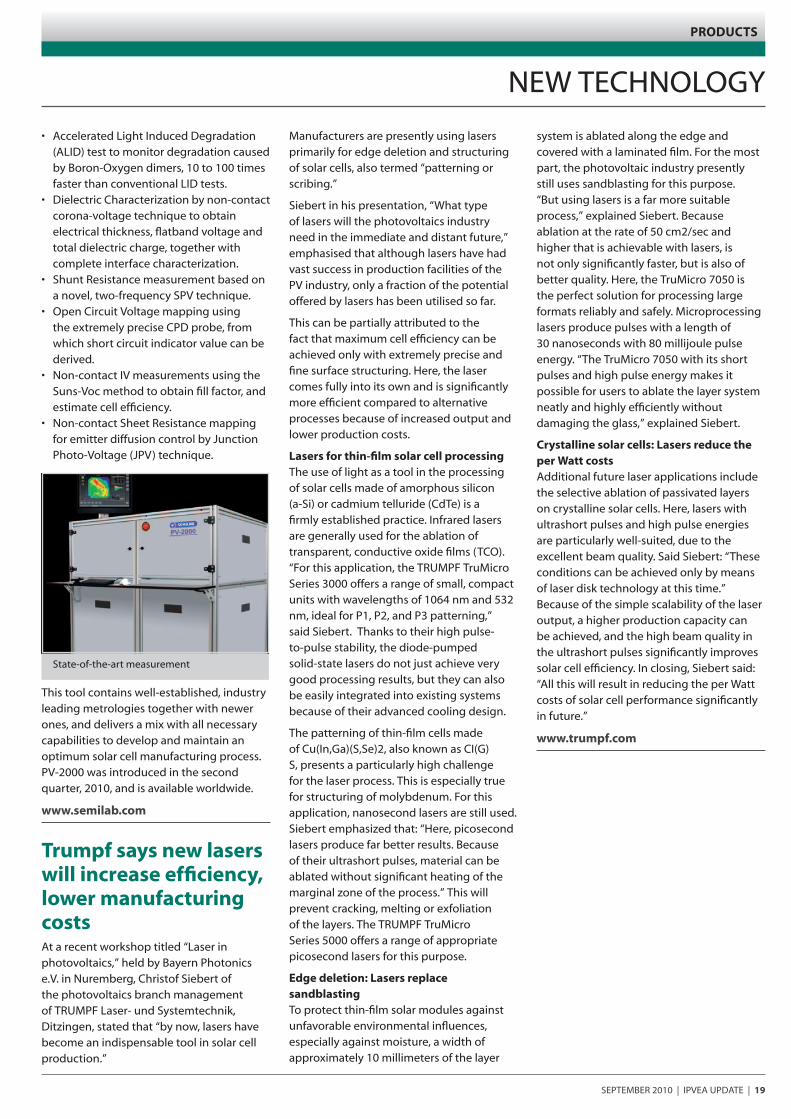
ProductS
new technology
sePtemBer 2010 | IPvea uPdate | 19
• accelerated light Induced degradation (alId) test to monitor degradation caused by Boron-oxygen dimers, 10 to 100 times faster than conventional lId tests.
• dielectric characterization by non-contact corona-voltage technique to obtain electrical thickness, flatband voltage and total dielectric charge, together with complete interface characterization.
• shunt resistance measurement based on a novel, two-frequency sPv technique.
• open circuit voltage mapping using the extremely precise cPd probe, from which short circuit indicator value can be derived.
• non-contact Iv measurements using the suns-voc method to obtain fill factor, and estimate cell efficiency.
• non-contact sheet resistance mapping for emitter diffusion control by Junction Photo-voltage (JPv) technique.
state-of-the-art measurement
this tool contains well-established, industry leading metrologies together with newer ones, and delivers a mix with all necessary capabilities to develop and maintain an optimum solar cell manufacturing process. Pv-2000 was introduced in the second quarter, 2010, and is available worldwide.
www.semilab.com
Trumpf says new lasers will increase efficiency, lower manufacturing costsat a recent workshop titled “laser in photovoltaics,” held by Bayern Photonics e.v. in nuremberg, christof siebert of the photovoltaics branch management of trumPf laser- und systemtechnik, ditzingen, stated that “by now, lasers have become an indispensable tool in solar cell production.”
manufacturers are presently using lasers primarily for edge deletion and structuring of solar cells, also termed “patterning or scribing.”
siebert in his presentation, “what type of lasers will the photovoltaics industry need in the immediate and distant future,” emphasised that although lasers have had vast success in production facilities of the Pv industry, only a fraction of the potential offered by lasers has been utilised so far.
this can be partially attributed to the fact that maximum cell efficiency can be achieved only with extremely precise and fine surface structuring. here, the laser comes fully into its own and is significantly more efficient compared to alternative processes because of increased output and lower production costs.
Lasers for thin-film solar cell processing the use of light as a tool in the processing of solar cells made of amorphous silicon (a-si) or cadmium telluride (cdte) is a firmly established practice. Infrared lasers are generally used for the ablation of transparent, conductive oxide films (tco). “for this application, the trumPf trumicro series 3000 offers a range of small, compact units with wavelengths of 1064 nm and 532 nm, ideal for P1, P2, and P3 patterning,” said siebert. thanks to their high pulse-to-pulse stability, the diode-pumped solid-state lasers do not just achieve very good processing results, but they can also be easily integrated into existing systems because of their advanced cooling design.
the patterning of thin-film cells made of cu(In,ga)(s,se)2, also known as cI(g)s, presents a particularly high challenge for the laser process. this is especially true for structuring of molybdenum. for this application, nanosecond lasers are still used. siebert emphasized that: “here, picosecond lasers produce far better results. Because of their ultrashort pulses, material can be ablated without significant heating of the marginal zone of the process.” this will prevent cracking, melting or exfoliation of the layers. the trumPf trumicro series 5000 offers a range of appropriate picosecond lasers for this purpose.
Edge deletion: Lasers replace sandblasting to protect thin-film solar modules against unfavorable environmental influences, especially against moisture, a width of approximately 10 millimeters of the layer
system is ablated along the edge and covered with a laminated film. for the most part, the photovoltaic industry presently still uses sandblasting for this purpose. “But using lasers is a far more suitable process,” explained siebert. Because ablation at the rate of 50 cm2/sec and higher that is achievable with lasers, is not only significantly faster, but is also of better quality. here, the trumicro 7050 is the perfect solution for processing large formats reliably and safely. microprocessing lasers produce pulses with a length of 30 nanoseconds with 80 millijoule pulse energy. “the trumicro 7050 with its short pulses and high pulse energy makes it possible for users to ablate the layer system neatly and highly efficiently without damaging the glass,” explained siebert.
Crystalline solar cells: Lasers reduce the per Watt costs additional future laser applications include the selective ablation of passivated layers on crystalline solar cells. here, lasers with ultrashort pulses and high pulse energies are particularly well-suited, due to the excellent beam quality. said siebert: “these conditions can be achieved only by means of laser disk technology at this time.” Because of the simple scalability of the laser output, a higher production capacity can be achieved, and the high beam quality in the ultrashort pulses significantly improves solar cell efficiency. In closing, siebert said: “all this will result in reducing the per watt costs of solar cell performance significantly in future.”
www.trumpf.com

We at Oerlikon Solar are proud to provide a new revolutionary solar technology that is ahead of its time. Be a part of the revolution and find out more about the new THINFAB and its world record breaking non-toxic, environmentally friendly solar technology at www.oerlikon.com /solar/thinfab.
Visit us at the EU PVSEC Valencia, September 6-10, 2010: Hall 2, Level 2, Booth Number B8
«Competition is not about winning. It’s about being better than the rest.»Robby Naish Youngest windsurfing world champion ever at the age of 13; the world speed record holder; continuously leading the world championship for more than 25 years

22 | IPvea uPdate | sePtemBer 2010
information
feature
heavy-duty dB schenker trucks are lining up in front of the factory
gates of the masdar Pv solar company in Ichtershausen near erfurt in
the state of thuringia in southeast germany.
they are laden with machines that together make up a complete
assembly line for the production of thin-film modules. these are
glass plates with a millimeter-thin layer that converts sunlight into
energy. construction is in progress all around the factory, as the long
winter has wasted precious time. to ensure that deadlines are met,
a whole lot of things are happening simultaneously. not only is time
short, but lack of space is also an issue because of all the diggers,
forklifts, and trucks. the wooden paneling of the 40-ton main
chamber of the system has been labeled as “very delicate cargo.”
this chamber will later be used to coat glass plates with amorphous
silicon under high vacuum.
“the solar sector is currently completely fixed on thin-layer
technology,” says Bernd albinus, key account manager of the solar
logistics division at dB schenker in dresden. “It requires a small
amount of silicon but produces powerful solar modules.” In the next
step, masdar Pv will structure the large modules – measuring up to
5.7 square meters – using a laser to produce hundreds of little solar
cells.
“the end customers of these modules are the large solar parks that
are developed in open-air spaces, or on large roof surface areas of
real estate,” says albinus. It is almost impossible to hear what he
is saying, as compressed air is being pumped into the air cushions
that dB schenker assembly engineers have pushed under the pallet
floor of the main chamber. as if by magic, the 40-ton chamber is
raised. forklift driver then pulls the enormous “floating” box into the
factory hall. the men push the machine the last part of the way by
hand toward the lifting frame operated by rober reh. done! torsten
Kröller from the us company applied materials, the manufacturer
of sensitive and valuable solar machines, nods in approval. dB
schenker transported the load from santa clara, california (u.s.),
to hamburg (germany) by sea, and then safely on to Ichtershausen
(germany) by heavy-duty truck and police escort on the highway
at night. the load was subsequently placed in its precise location in
the customer’s factory by dB schenker. a difficult job. But easy ones
generally do not exist in solar logistics.
the entire solar sector is embedded in a complex supply chain. It
ranges from the production of silicon up to the completed solar
electricity module. accordingly, the companies involved in the
sector are just as varied, and include manufacturers of silicon, silicon
wafers (the carrier disks for solar cells), cells, modules, and thin-
layer technology. “the multi-layered requirements placed on solar
logistics each demand tailor-made solutions in the supply chain that
meet top-quality standards,” says Joachim marxer, vice President of
global vertical market semicon/solar at dB schenker. the range of
services supplied by dB schenker solar logistics experts varies from
transporting machines by heavy-duty truck to delivering individual
materials such as glass, frame sections, and consumables. when
transporting the finished components, solar logistics experts must
work with extreme care.
www.dbschenker.com
Logistics in the Solar Supply ChainDb Schenker logistics experts run the entire supply chain of the solar industry.
This includes from small screws up to transporting machines that weigh many tons.
text & pictures © dB schenker

sePtemBer 2010 | IPvea uPdate | 23
nEWS
eXclusIve IntervIew
euPd examines the uK market
IPVEA Update: The introduction of feed-in tariffs – taking the German EEG as a prototype – in April this year, stirred up hope among several photovoltaic companies for a new sales market. Can the British PV market fulfil expectations?
MH: the introduction of feed-in tariffs could finally mark the beginning of a Pv market uptake in the uK. due to the elaborated design and a maximum system size of five mw, we expect steady and sustainable market
development. germany (before 2009), france or Belgium might serve as role models, rather than stochastic large-scale peak markets such as spain or the czech republic.
What do companies have to keep in mind when planning their market entry in Great britain?MMW: for Pv companies willing to enter the promising uK market, time is a decisive factor. a situation in which most module and inverter manufacturers are sold out – sometimes until the end of 2010 – provides a valuable opportunity to foster activities in newly emerging markets. By occupying sales channels and building brand awareness, barriers for later market entrants can be installed. a fundamental prerequisite of market uptake for module manufacturers is the provision of mcs certifications.
MH: for the small-scale segment – systems up to 50 kw – we consider sales channel architecture and financing to be key. In the current uK market, long-term supply contracts are still an exemption, and most installers indicate that they expect their procurement channels to change in the near future. In such an environment, building up regional networks of existing installers and, at the same time, attracting new companies to enter the Pv installation business (e.g., by
co-funding the mcs certification fees) will establish stable distribution channels.
What is behind the concept of MCS certification?MH: that’s a new certification system for sustainable energy products that recently has been introduced by the government. the program is called the ‘micro-generation certification scheme’ (or mcs) and aims to protect end customers by ensuring a level of quality in both products and installations. the scheme works by putting manufacturers and installers through an inspection process in which the applicant has to demonstrate a certain level of competency in the technology that is offered. Installers and distributors must provide a documented, quality management process and show an example of a finished installation or product.
“For PV companies willing to enter the promising UK market, time is a decisive factor.”Markus A.W. Hoehner
Where is current system price span for private system operators in the british PV market?MH: with regards to pricing, the uK’s small-scale segment is currently characterized by two opposing trends: wholesale prices are only slightly (approx. 10-15%) above the level in germany. end customer system prices, on the other hand, can be up to 4,600 euro – over 50% more than the german average price for small installations. Part of this difference could be based on the lack of experience uK installers have and the resulting increased time requirements and costs of an installation. at the same
time, the currently low level of competition apparently allows them to realize significant margins.
only plants up to 5 mw in size will be funded. Is the market therefore profitable for professional investors?
MMW: the large-scale project business will, as in other markets, be triggered by return on investment. the level of solar radiation and the comparably high fIt level will facilitate Irrs distinctly above the
required bottom line of ten percent. actual rates will largely depend on the system prices and the fees charged by the grid operator. module prices for 3q|2010 for large-scale systems in the uK are about the same as can be observed in germany. the range is from about 1.35 eur/kw for chinese tier one modules to 1.65 eur/kw for german premium brands.
MH: fees for grid connection are not homogeneous. depending on the individual grid operator, they can be as high as £875,000 (gBP) for a 5-mw plant. another boundary condition surely is that maximum system size is limited to 5 mw and that – unlike the “huertas solares” in spain – it is not possible to combine multiple plants to form one large solar park. despite this limitation, we expect that as of 2011, the uK market will increasingly attract project developers and investors wishing to develop large-scale Pv projects.
Further information on entering the British PV market, political framework conditions, as well as drivers and hurdles to successful development can be found in the new study of EuPD Research. www.eupd-research.com
“the uK Photovoltaic market 2010 – tapping the fullest Potential.”
In 2000, markus a.w. hoehner founded hrcg gmbh as a market research and consulting company. under this umbrella,
360|consult is the consultancy division of the company while euPd research provides market research services.
the service portfolio of 360|consult covers all aspects of strategy consultancy, specifically the analysis of market
structure and market segmentation, the analysis of competitors and customers as well as consultancy with regard to the
strategy implementation process.
In this exclusive interview, on the anniversary of the company’s 10th anniversary, IPvea update talks with hoehner,
who holds the title of ceo and founder of hrcg, the holding company of the operating brands euPd research and
360|consult, and markus monssen-wackerbeck, director of 360|consult, about the outlook for the British Pv market.
markus a.w. hoehner
markus monssen-wackerbeck

24 | IPvea uPdate | sePtemBer 2010
EXEcutiVE intErViEW
…Views from IPVEA member executives
Member Profiles...
Serving the optical disc market with raw materials since 1986, Targray Technology International Inc., based in Montreal, Canada, was sensing the need to diversify by 2005 when volumes for physical media started hitting a downward trend that showed no sign of rebounding.
“we were looking for another industry to diversify into,” explains targray president andrew richardson. “we had a business model for the cd industry and a global worldwide network. we were looking what we could leverage to go into a growing industry. after an extensive search, we found solar. ”
the Pv solar business reminded richardson of the where the cd industry was circa 1986 – still relatively new, but on the verge of a very big growth curve.
“It was not mature in terms of its manufacturing processes yet. there’s still room for innovation. there are lots of materials used,” he adds.
some materials needed for thin-film Pv, in fact, targray already supplied, such as targets and silicon, for optical discs. “we’re probably the largest supplier of targets to the cd industry, at least aluminum targets,” notes richardson, adding targray also supplies silver targets.
“we’ve been in that business a long time, and done a lot of innovations in it. we knew we had a first product to get into the Pv industry. we also could get silicon, and there was a silicon shortage. so with two products, we had a very good place to start. It ended up being a very good move: today the Pv business is the largest part of our business, significantly more than 50% of our revenue today.”
targray didn’t see the need to hire Pv specialists. “we put some of our own people and dedicated them on the Pv industry. I learned a lot about it going to shows. Because we had those initial products, we had access to customers. By visiting customers and understanding their needs in depth, we could build out the rest of our product line. starting out with the targets and the silicon we were able to learn enough about the industry to develop more products. through continuous customer contact, we have a wealth of information about customer requirements.”
richardson notes that targray’s business model is supplying all the raw materials for a specific industry. as a result, his company gets “to visit customers 10 times more than our competitors.” typically, targray visits customers 10 to 15 times a year.
“a meeting typically takes all day. In Pv you might meet with the person in charge of cell processing, the qc manager, the person doing the lay up with the encapsulants, the engineering manager,
the purchasing person, distribution for the cells, the parts people. our business model allows us get a lot more information.”
when starting out with Pv manufacturers, targray was able to demonstrate innovations the company had done with targets in the optical disc manufacturing, such as better grain size, better uniformity of the layer that gets deposited, and longer life of the targets.
“that’s pretty compelling for a manufacturer looking for a targets supplier,” says richardson. “we were able to convince people to know that we had the knowledge to make better products for them.”
like nearly everyone else in business, richardson explains that 2009 was not a very happy year. “Because of the financial crisis, many of our customers were still in the position if having to raise money or in the middle of a big expansion. when the brakes hit, they were still committed to buy a lot of equipment and materials. some customers had to make write-downs on materials, silicon especially, that they had in stock. It really hurt a lot of our customers. our customers in 2009 stopped buying consistently. some people shut down their module facilities. some people shut down their cell facilities and went from 100% production to 20% or 40%. some stopped all together, depending how competitive they were or how strong their brand was. customers who we were depending on for regular sales, all the sudden had no money and just couldn’t buy in some months. so as a result, prices declined on many products, especially silicon, and volumes declined as well.”
how much did the price drop for silicon in 2009? targray’s silicon volume actually increased in 2009 compared to 2008, but the price declined more than the volume increase.
“so 2009 was very rough year and something we had to get through because a very large percentage customers had no liquidity. that’s changed in 2010. even the end of 2009 was much better. and 2010 has been much stronger. If I had to grade it as a year, I’d say 10 out of 10 at the mid-way point in terms of demand and volume. you can imagine a nightmare scenario where every government in the world rescinds their feed-in tariff. oil goes down to $10 a barrel and people forget there’s such thing as global warming, but I don’t think it’s a very likely scenario. I think there will be some years that the industry will have 100% growth and
How one company found its way to solartargray’s andrew richardson

sePtemBer 2010 | IPvea uPdate | 25
others 20%, and maybe others it will be 5% but we haven’t seen that yet. In the long run, I think you’re going to see continued large growth over a long period for Pv.”
richardson still is cautiously optimistic for 2010, as the result of such as developments as germany lowering their feed-in tariff rates, effective 1 July. “People are wondering how that will affect the industry. I think we would have started seeing something already. we’re still seeing strong demand in all parts of the world in the u.s., china and asia in general, and also in europe. so we still think the rest of 2010 is going to remain strong, somewhere between and 8 to 10 out of 10 in terms of volume and demand.”
he attributes the rebound to the global economy improving and banks in general lending more, notwithstanding some remaining fiscal problems in europe, such as greece.
“the liquidity means customers can buy. the investment in a solar farm, for example, which is guaranteed by a utility, which is guaranteed by a government, is quite a safe investment. once the banks were over their shell-shocked mode after the financial crisis they started lending to these kinds of projects.”
attributing the rebound also to the price decline in final module, richardson cited the price of silicon declining from us$450 a kilo to something closer to $50 a kilo, as well as improvements in efficiency.
“that reduces the cost of the whole system when you can generate more watts with the same size cell using the same amount of materials. that increases the yields for the investor who can buy modules at a price 30% less than a year ago. your return stays the same at what you’re going to sell your electricity for, and your investment yield increases significantly and it makes it much more attractive for investors to invest in Pv. that’s what is driving the dramatic growth we’re seeing this year in the industry.”
when asked what was the last book he read, richardson, not surprisingly mentions a business title, although it’s not a printed book. rather he’s picked up the habit of listening to audiobooks whenever he has some spare time – during a run, exercise, or driving in his car.
“so I’m now ‘reading’ about one or two books a week. the one I think had the most impact is called The Leadership Pipeline by ram charan, stephen drotter, and James noel. It’s about building an organisation, and how to build the leader to allow you to grow. It’s not a new book, about 10 years old, but very well done and we’re starting to use it in our business.”
www.targray.com
richard hendel has been working for rofIn Baasel lasertech for all of his professional career during the past 20 years.
In fact, he even worked for the company while he was earning his engineering degree from the fachhochschulemünchen.
he currently holds the title of rofIn’s sales manager of solar technology, and has long-term experience working with highly sophisticated laser applications.
hendel started his career 1991 at carl Baasel lasertech’s r&d department and worked his way up through various product development and sales positions at Baasel lasertech, and later rofIn, including a two-year stint in a sales position at the company’s u.s. headquarters in michigan.
rofIn has 33,000 systems installed worldwide, making it, according to the company, the leading manufacturer of laser sources and laser-based solutions for industrial materials processing including laser cutting, laser welding, laser marking and surface treatment.
this IPvea update interview found hendel preparing for an open house that rofIn was sponsoring 8-10 June at its stornberg, germany headquarters. they’re expecting to entertain approximately 80 existing and prospective customers, as well as manufacturing partners. following an introduction to the company by rofIn chief operating officer thomas merk, hendel made a presentation entitled “Introduction to laser Processing of solar cells.”
at the open house, visitors had the opportunity to get a deep look at rofIn’s application lab demonstrating some practical applications.
rofIn had considered to exhibit at Intersolar europe in munch on 9-11 June. Instead, rofIn figured that hosting its own open house would be a much better way to get key individuals’ undivided attention than competing with everything going on at a large trade show.
“[this year business] has rebounded very nicely,” hendel says, noting that in the beginning of 2009 “things looked very ugly, but began to pick up in the spring.”
the rebound has been driven by asian growth, china in particular, he says.
hendel is pleased that his solar energy-oriented livelihood can contribute to the betterment of the environment.
“I’d have a problem making buttons for tanks, or knowing that people could get killed with my lasers. what I do with the company gives me a good feeling,” he adds.
EXEcutiVE intErViEWS
InsIde IPvea
rofIn’s richard hendel

26 | IPvea uPdate | sePtemBer 2010
information
insideWelcome to inside IPVEA, our regular section where you can find the latest news, views and information from within iPVEA. if there are any features you would like to see added to inside IPVEA please email [email protected]
IPVEA Members’ Meeting8th september 2010, 8:30am - 9:30amlocation: sala ausias march, in the exhibition area (entry foro centro) of the feria valencia, valencia feria, spain
IPvea companies are reminded of the next members’ meeting to be held on the 8th september in valencia and are cordially invited to attend. the agenda for the meeting is below and the fore mentioned documents regarding the last members assembly minutes and financial year will be available in the member’s only section of the IPvea website www.IPVEA.org
AGENDA: • welcome• ascertainment of correct convocation, decision about the
agenda• approval of the last members’ assembly’s minutes• reports about the financial year 2009 -2010• discharge of the Board of directors for the financial year
2009- 2010• election of Board of directors • report from the technical committee• discussion as to which industry events to support in 2010• miscellaneous
IPVEA supported event SNEC extends to 12 halls in 2011following the previous success of four snec events, shanghai new energy Industry association (sneIa) plans to hold the 5th snec International Photovoltaic Power generation conference & exhibition Pv Power eXPo from 22 - 24 february 2011 at shanghai new International expo center (snIec), china.
It is expected that there will be 12 halls w1 thin-film; w2 silicon material, w3-w5 silicon-based modules; e1-e2 system e3-e7 equipment.
IPvea members receive a special discount on space of $280/ sqm (non-member price is $320/sqm).
IPvea members are asked to contact tom qin direct if they are interested in space.
cell: +86-13381813477 e-mail: [email protected]
New co-chair of IPVEA technology committeevolker wüstenhagen, head of advanced nanotechnology, vice President, oc oerlikon Balzers ag., is now co-chairing the IPvea technology committee with Bill duncan, director of Project management Komax systems.
Solar Power conference discount for IPVEA membersIPvea has arranged for its members to receive a 15% discount on the full conference rate at solar Power International. to receive this discount members are required to enter the code “PtnmBrsPI10” when registering online.www.solarpowerinternational.com
IPVEA to vote for new board Members IPvea members will elect new Board of directors in valencia at the 25th european Photovoltaic solar energy conference and exhibition (eu Pvsec) during the IPvea members’ meeting on september 8, 2010.
the meeting will be held at 8:30 am at “sala ausias march” in the exhibition area (entry foro centro) of the feria valencia, and should not last more than an hour. we kindly ask that at least one representative is in attendance from your company.
stepping down from the board are mannford schroder, albert vontz and hans Jürgen stang.
the new candidates to be voted on include:
Bill duncan – Komax solar, Inc.Peter Kiemstedt – Kuka systems gmbh Patrick Binkowska – singulus/stangl solar gerhard dovids – rIcmar technology gmbhcarsten Busch – aBB automation gmbh ortrun aßländer – acI-ecotec gmbh & co. Kg ludger wahlers – Isra vIsIon

marKet uPdate
sePtemBer 2010 | IPvea uPdate | 27
nEWS
Programme may be subject to change
vlsI research – Pv equipment forecastoverview 2010by andrew thomas
2010 should be another boom year for suppliers of Pv manufacturing equipment. sales are being driven by dramatic falls in cell prices and vlsI research is forecasting a growth of 14% in the market for cell and module equipment and a growth of 21% in the market for polysilicon, ingot and wafering equipment. the expected result is an all time high for the industry with sales reaching a value of $8.5Bn.
It’s not all good news though as the market for silicon thin film equipment is predicted to have a poor year in 2010 after two years of terrific revenue growth in 2008 and 2009. overcapacity
and cost issues are starting to have a negative impact on the market with sales forecast to decline by 37% in 2010 and to stay at depressed levels until these problems have been resolved.
In the market for non-silicon thin film on glass equipment first solar continues to be the primary driver although new turnkey lines from centrotherm, roth and rau and veeco should see the entry of new players. this is going to be the strongest sector for equipment suppliers with growth in the region of 42% expected for 2010.
looking further out, 2011 will be another year of challenges for the industry. governments, particularly those in europe, are facing tough budget decisions and will come under increasing pressure to slash funding. Pv panel and module prices are falling which makes the Pv industry an easy target for cuts and the risk is that if they cut too far and too fast this could seriously hold the industry back.
vlsIresearch inc’s database on Pv manufacturing equipment is a web-based subscription service providing a detailed insight into the fast moving world of photovoltaics from the equipment
supplier’s perspective. It includes data and analysis covering the entire Pv manufacturing process from polysilicon manufacture to final test, with separate data for each of the major cell technologies. the focus is on the measurement and forecasting of demand for process equipment and includes capital equipment supplier market shares split by equipment category and by cell technology. In addition, sales of turnkey lines are tracked by vendor and cell technology. the service also provides detailed information on Pv cell and module manufacturing and other key market drivers.
VLSIresearch inc’s Database on PV Manufacturing Equipment
is a web based subscription service providing a detailed insight into the fast moving world of photovoltaics from
the equipment supplier’s perspective. It includes data and
analysis covering the entire PV manufacturing process from
polysilicon manufacture to final test, with separate data for each
of the major cell technologies. The focus is on the measurement
and forecasting of demand for process equipment and includes capital equipment
supplier market shares split by equipment category and by cell
technology. In addition, sales of turnkey lines are tracked by
vendor and cell technology. The service also provides detailed
information on PV cell and module manufacturing and other
key market drivers.
Tel: +44 1234 834666
12000
10000
8000
6000
4000
2000
02004
821 1211 1961
4030
8789
7707
8828
980210415
2005 2006 2007 2008 2009 2010 2011 2012
PV Manufacturing EquipmentSales in $M per Calendar Year
$M

tEcHnoLoGY
whIte PaPer
28 | IPvea uPdate | sePtemBer 2010
Sustainable Quality for Long-Term Investments
Photovoltaic (Pv) systems take many years to prove their worth as an investment. only if they cover the costs of the acquisition by constantly supplying energy, the decision to purchase a solar energy plant is justified. In some cases presumably small details, such as the adhesives, sealants and potting compounds used, may impair the service life of a solar module.
even if these products account for only a fraction of the production costs, they nevertheless play an important role regarding construction and functions: they keep the glass surfaces in the metal frame, fix assembly rails and junction boxes in place, seal and bond the corners of the module frame, and as potting compounds they protect the sensitive contact points within the junction box. a faulty construction may entail the loss of function of the complete module and hence give rise to demands for compensation, quite apart from damaging the company’s image.
Potting of the junction boxes with 2-component silicone compoundsIn the past precisely the junction boxes, which divert the current from the module and feed it into the grid, have frequently brought about failures or caused the module to temporarily or completely lose its ability to function. to ensure that the junction box functions for the entire
service life of a module (i.e., far longer than 20 years), it is of prime importance to permanently protect the contact points at which the electricity is tapped in the box. this means effectively and permanently preventing moisture and dust from penetrating the box. this is not always the case for the entire service life of boxes sealed only by means of a rubber seal in the lid area.
silicone-based potting compounds (fig.1) offer the best protection because they envelope the contact points directly. If a suitable sealing compound is selected and correctly used, the functionality of the module can be ensured for its entire service life.
elastic silicone potting compounds with good self-adhesion on glass and backsheet films have been developed for this application. to ensure adhesion on the junction box otto offers free tests in the company’s own laboratory. In addition to excellent resistance to weather, aging and uv, the silicone-based elastic potting compounds also provide permanent temperature resistance up to 150 °c and outstanding electrical (insulation) properties. thanks to the elasticity of the materials, vibrations and expansion owing to thermal fluctuations can be permanently and reliably compensated.
By Nikolaus Auer, Edgar Werner
otto-chemIe
OTTO has been developing and manufacturing silicone adhesives, sealants and potting compounds for more than 45 years and is one
of the leading suppliers to the international solar industry. OTTO offers a wide range of tailor-made
solutions in one and two-part silicones for any kind of bonding,
sealing and potting application in the PV industry.
More details as well as literature are available from
www.otto-chemie.de
1 Potting of the junction box 2 Bonding of the junction box

tEcHnoLoGY
whIte PaPer
sePtemBer 2010 | IPvea uPdate | 29
against the background of falling module prices – besides the protection of the contact points against environmental influences and the outstanding electrical properties – the production costs and efficiency are crucial production factors. In this case potting compounds, which make it possible to handle the boxes after filling them with short buffering times, provide an opportunity to cut costs. these potting compounds react at room temperature, i.e. without additional energy costs for heat or uv activation. the viscosity is adjusted to enable it to flow reliably around even tight undercuts. the potting compounds can be processed fully automatically using mixing and dosing systems. the reactivity and viscosity can be adjusted individually to cater to the production process of the respective customer.
bonding of the module frame and of the junction boxesthe attachment of the junction boxes to the backside of a Pv module (fig.2) as well as of the module frame to the glass (fig.3) is achieved by using one or two part silicone adhesives.
bonding assembly rails onto PV modulesalso when assembling the Pv modules to form solar energy plants, extremely reliable joining techniques are essential. high
and fluctuating forces affect the modules and therefore also the fixing points for decades. when building large-area Pv energy plants, rail systems consisting of a carrier rail and a back rail are becoming increasingly popular. they make it possible to largely prefabricate the products under the controlled conditions at the factory and to assemble them quickly on-site. the Pv modules, which are equipped with a back rail in the factory, can be connected fast and securely with the elevated substructure on which the carrier rails rest (fig.4).
Broad performance profile requiredsilicones for the production of Pv modules and plants all over the world and in any place must withstand both extremely fluctuating temperatures and weather and high uv exposure. Besides this, as well as suction and pressure loads from the wind, ice and snow and, last but not least, the fact that at fluctuating temperatures which inevitably occur, glass and metal have different expansion coefficients. the bonding technique is absolutely predestined for this connection between glass and metal because elastic bonding is capable of compensating a change in the length of the materials. another advantage of the assembly rails fastened to the back is stabilisation of the frameless thin layer modules in themselves.
high temperatures inevitably affect Pv modules. the back rail adhesive ottocoll® s 640 provides very good thermal stability. according to ul (underwriters laboratories) the adhesive has an rtI value (relative thermal index) of +105 °c, and in-house tests have shown a permanent thermal stability of -40 to +180 °c. furthermore, it corresponds to the ul flame classification hB (file no. e176319).
owing to the affinity with glass, high quality silicones demonstrate very good adhesion on glass. extensive long-term investigations have been carried out to establish the adhesive power on diverse metal surfaces such as anodised aluminium and various qualities of galvanisation. the result: despite extreme strain the adhesive showed no significant signs of fatigue and is far above the standard values required by international institutions (e.g., etag). last but not least, the cantilevered bonding of the assembly rails, i.e. without any mechanical safeguard, requires an adhesive that offers sufficient safety potential with regard to its creep properties. this was also tested extensively, permitting the relevant design values for dimensioning the bonded joint to be deduced. Project-specific support is offered for this purpose.
© Hermann Otto GmbH 2010
3 Bonding the module frame 5 Sealing of module corners4 Effective connection of the back rail and the substructure

tEcHnoLoGY
whIte PaPer
30 | IPvea uPdate | sePtemBer 2010
Selectively Dopedlaser technology enables mass Production of solar cells with selective emitters
with spot market prices in the range of 1,50 to 2 € / wp for crystalline modules and about 1,50 € / wp for thin film modules the photovoltaic market shows a 30 to 50% decrease in prices within one year. as several governments announced a significant reduction of feed-in tariffs this development will progress further. for thin film cell manufacturing, which reached mass production scale several years later, there is still some fundamental cost cutting potential. like the continuous roll-to-roll production of flexible solar cells, which is one of the most promising approaches. for this technology rofIn offers a new, highly customizable roll-to-roll system, which handles step and repeat processes as well as on-the-fly applications.
Efficiency Improvement on c-Si Cells in the Focus Againcost reduction potential in crystalline cell manufacturing is comparatively small. current activities focus on saving of material (e.g., thinner silicon wafers or less silver paste in screen printing, reduction of production waste and further increase of plant availability). But all these approaches share a rather limited cost reduction potential.
as a consequence, manufacturers draw their focus on the second component of the price/wp: improving the efficiency. the range of promising technologies is wide, as various high-performance cell concepts demonstrate efficiencies of > 20%. But in mass production the efficiency gain has to outmatch necessary additional investments.
Photovoltaic manufacturers as well as production line suppliers are optimizing their process flows and introduce additional process steps that enhance the cell efficiency. Ideally the new processes shall be retrofit able for existing production lines. material processing with lasers is one favourable technology to do this. compared to etching and diffusion steps, laser machining offers perfect process control, it is cost-efficient and gentle to the material. as a clean and flexible technology, integration in existing production lines is quite easy.
rediscovery of Selective Emittersthe most promising solution these days is age-old in photovoltaic timescale. It focuses on selective emitters – already discussed in the late 70s. selective emitters promise efficiency gains of up to one percentage point (up to 17% for multi-crystalline and 18.5% for mono-crystalline cells).
today, bulk production solar cells show an entirely metallized rear surface, a thick p-type doped layer, a thin n-type silicon layer, passivation and anti-reflection layers and a front side contact grid. In detail there is always a tradeoff between the desired heavy n-type doping underneath the metallized contact regions and light doping between the contact fingers. heavy doping achieves low contact resistance and good lateral conductivity whereas light doping is necessary for limited recombination and good response to blue light. as a consequence, in this short wave spectral range solar cells do not convert almost a third of the photons into charge carriers.
Selective Emitters for Mass Production Scalethe solution has been long obvious: the selective doping of emitters. on the other hand it has been common sense as well,
that selective doping is way to complex for mass production scale. additional doping to achieve different doping levels complicates the production process with several steps (masking, diffusion, etching). moreover, it requires perfect alignment of heavily doped regions with the screen-printed contact fingers by most precise process technology.
recently several new approaches emerged, which avoid the disadvantages mentioned above. the big german integrators and turnkey suppliers – roth & rau, manz, schmid and centrotherm, among them – spend a lot of effort on this subject. with china sunergy, even one of the leading manufacturers integrated selective emitters into mass production. Besides etch-back technology, which forms a highly doped uniform emitter that is then selectively weakened via etching, all selective emitter concepts rely on laser material processing.
Laser Ablation Enables Selective Dopingdiffusion masking is one of the most advanced concepts so far. Previous to dopant diffusion, it generates a dielectric masking layer, which is then selectively opened by lasers in the later contact areas. thus the following diffusion step creates different dopant concentrations on masked and non-masked areas.
a major production line supplier picked this technology after an evaluation of various concepts and presented diffusion masking at the 24th european Photovoltaic solar energy conference, in september 2009. a laser ablates the dielectric layer in lines slightly wider than the contact fingers which are screen-printed subsequently. for optimum results the laser process has to combine high speed and throughput with minimum damage of the silicon underneath.
By richard Hendel, rofIn’s sales manager
of solar technology

tEcHnoLoGY
whIte PaPer
sePtemBer 2010 | IPvea uPdate | 31
Direct Selective Laser Dopingdirect selective laser doping is a promising concept for realising selective emitters as well. as lasers generate precisely controlled, localised heat input, they offer optimum prerequisites for a selective doping process. early concepts combined lasers with liquid or gaseous doping sources which demanded elaborate process technology. In contradiction, new approaches use a „dry“ process (e.g., localised melting and incorporating of predeposited solid-film dopants).
the easiest solution, already presented in the 90s, uses the phosphosilicate glass (Psg) layer, already grown on top of the emitter during conventional dopant diffusion, as doping source for a second step. a laser locally melts the silicon surface underneath and allows for additional phosphorus diffusion from the Psg layer into the emitter. however, the challenge of aligning heavily doped emitter areas with the contact grid remains. other approaches apply a phosphorous doping source on top of the dielectric layer just before front contact forming. a laser melts the silicon lying beneath, incorporates the phosphorus dopants into the molten silicon and removes the dielectric layer thereby exposing the silicon surface for subsequent self-aligned metal contact formation.
Green Lasers and Innovative Fiberssolar cell processing pushes laser technology to its limits with regards to beam quality, output power and pulse frequency. q-switched and diode pumped solid-state lasers are the preferred tool for these applications. for optimum interaction with dielectric thin films, frequency-doubled lasers are commonly used. fine-tuning of pulse length and energy is essential for most selective ablation. the short cycle times, which are standard in mass production of solar cells, require laser sources up to 100 watts of output power, depending on application.
contrary to solid state lasers with fundamental wavelength of 1064 nm, frequency-doubled green lasers with 532 nm show the desired near-surface absorption in silicon within 1 µm depth. frequency-tripled, near uv sources offer improved absorption characteristics to some extent. But uv-qualified optics
are rare, the selection is small and their lifetime is comparatively short - suboptimal preconditions for industrial mass production.
current projects, conducted by research institutes and solar cell manufacturers, prove that rofIn‘s new Powerline l 100 shg source with 532 nm is perfectly suitable for selective ablation of dielectric layers as well as for direct laser doping. new optical fibers, especially developed for this wavelength, play a central role in this case. realising a top-hat beam profile, they provide homogenous energy distribution within the entire laser spot area. thus the intensity of ablation and diffusion processes is significantly more consistent.
Conclusionfor laser manufacturers photovoltaics is a promising and demanding market at the same time. new high-efficiency cell concepts as well as optimizing technologies for mass production require tight cooperation between research institutes, production line suppliers and solar cell manufacturers. with selective emitters, a well-known approach, already tested in high-efficiency cells, finds its way to mass production. It won’t be the last. the laser is a key technology for a magnitude of tried and tested high-efficiency concepts, from laser-fired contacts to laser-buried contacts to back-contact cells.
more than that, selective doping and selective ablation of dielectric layers with the laser generally opens a broad field for new efficiency improvement approaches. In many cases, they will focus on the redesign and optimisation of front and back-side contacting. as selective ablation works with layer thicknesses from 10 to some 100 nm, the requirements on laser-beam quality, pulse-to-pulse stability and long-term stability are huge. this will be a driving force for the development of laser sources that are optimised for photovoltaic manufacturing, like rofIn‘s Powerline l series.
1. opening of a dielectric layer with typical finger grid
2. Principle of selective emitter
3. 2 sem picture of Psg-doping
4. 3 Powerline l with fiber beam delivery and scan head
www.rofin.com

tEcHnoLoGY
whIte PaPer
32 | IPvea uPdate | sePtemBer 2010
Does the Solar Industry Need High Purity Performance Chemicals?
high purity chemicals will become increasingly important as Pv manufacturers drive toward grid parity.the financial crisis of 2009 saw module asP’s collapse by up to 40% compared to pre-crisis prices seen in 2008. these lower prices have driven module, cell, and wafer manufacturers to require lower prices from their upstream suppliers as well as from their process chemical vendors. throughout the solar cell manufacturing process, a variety of chemicals, including hf, hno3, naoh, Koh, Pocl3, h3Po4, sih4, and nh3 are utilized. figure 1 illustrates some of these chemicals and where they are used in the cell making process.
figure 1. Process flow digram for standard solar cell
manufacturing.
It was only a few years ago that solar cells were made using recycled or rejected silicon from the semiconductor industry. these cells were usually made in warehouses and treated with commodity chemicals. flash forward to 2010 and the industry now consumes more polysilicon than semiconductor - no more hand-me-downs for us. furthermore, the cells are processed in clean rooms that rival some of the most sophisticated semiconductor fabs. why then is the solar industry satisfied with chemicals that are of lower purity than the silicon wafers now in use?
to achieve the increases in solar cell efficiency and production yield required
to achieve grid parity, the industry must continue to turn to high purity performance chemicals used in texturing, emitter formation, phosphosilicate glass (Psg) removal, arc deposition and metallization.
the remainder of this article will focus on the phosphorus diffusion step and the advantages of using a performance chemical for the solar cell manufacturer.
Phosphorus Diffusionthe traditional P-n Junction is formed by diffusing phosphorus (an n-type dopant) onto a Boron doped (P-type) silicon wafer. this diffusion can occur in a batch diffusion furnace using phosphorus oxychloride (Pocl3) or in an inline furnace using a spray-on phosphoric acid (h3Po4). It is the formation of the P-n Junction that enables
the generation of electricity through the photovoltaic effect.
once a photon hits the top of the solar cell, an amazing series of events must take place for
electricity to be created. first, the photon must be absorbed by the semiconductor material. this will only happen if the photon is not either reflected off the surface of the cell, or passed through the cell entirely. next, the absorbed photons must be converted to charge carriers.third, charge separation of the carriers must take place within the cell (at the P-n Junction). finally, the carriers must be extracted as electricity through an external circuit before they are lost through carrier recombination.
a significant amount of research has been conducted that has established the correlation between minority carrier recombination lifetime and the ultimate efficiency of the solar cell. this correlation has been demonstrated regardless of the type of wafer whether it be monocrystalline,
or multicrystalline. there are currently several test available that can be conducted inline on a production solar cell line, or offline using a stand-alone testing unit to test for minority carrier lifetime at each step in the cell manufacturing process. for example, the quasi-steady-state area-averaged lifetime measurement method has been proven to effectively predict the ultimate cell efficiency in multicrystalline cells. for more details on this see sinton, r.a., “Predicting multi-crystalline solar cell efficiency from life-time measured during cell fabrication”, Proceedings of 3rd world conference on Photovoltaic energy conversion, 2003. p. 1028-1031, volume 2.
It has also been established that impurities found in the silicon wafer or introduced by the phosphorus diffusion process will contribute to recombination and a lower minority carrier lifetime test result after the diffusion process. specifically, the existence of 3d transition metals have been found to dramatically reduce lifetime. for example, mchugo, thomson, Perichaud and martinnuzi found a direct correlation between regions of high concentrations of Iron, chromium, and nickel and areas of high minority carrier recombination in multicrystalline cells. “direct correlation of transition metal Impurities and minority carrier recombination in multicrystalline silicon” http://www.als.lbl.gov/als/compendium/abstractmanager/uploads/madalsd.pdf. a study by westinghouse research laboratories found that the worst lifetime killers are, in order of decreasing severity, molybdenum, titanium, vanadium, chromium, manganese, iron, aluminum, nickel, copper, magnesium, zinc, and calcium. davis, J.r., rohatgi, a., rai-choudhury, P. Blais, P., and hopkins, r.h., 13th Ieee Photovoltaic specialty conference, washington dc. June 1978, p. 490.
which brings us back to the benefit of high purity performance chemicals. take for example the guideline specification
by Scott Schumacher, vice President,
Peak sun silicon

tEcHnoLoGY
whIte PaPer
sePtemBer 2010 | IPvea uPdate | 33
for Pocl3 intended to be used by the solar industry currently promulgated at International standards committees by commodity chemical manufacturers:
assay >99.9%
typical metals analysis (ppb)aluminum <10arsenic <10Barium <10Boron <10cadmium <10calcium <10chromium <10copper <10Iron <10lead <10lithium <10magnesium <10manganese <10nickel <10Potassium <10sodium <10tin <10titanium <10vanadium <10Zinc <10
now look at the data sheet for a high purity performance Pocl3 currently being sold by Peak sun silicon:
specificationsassay >99.9%Purity(metals Basis) >99.99999%color (aPha) <5typical metals analysis (ppb)aluminum <1arsenic <3Barium <1Bismuth <1cadmium <1calcium <3chromium <1cobalt <1copper <1gallium <1gold <1Iron <3lead <1lithium <1magnesium <2manganese <1mercury <5molybdenum <1nickel <1niobium <1Potassium <2silver <1sodium <5strontium <1tin <1titanium <1vanadium <1Zinc <3
real World resultswhile performance chemicals introduce significantly fewer impurities into the silicon wafer, during the diffusion process, the real proof is in the results experienced by customers using high purity chemicals in their production lines. review for example, the results from the customer below:
Carrier Lifetime• 156mm multicrystalline cells• lifetime measurement ~24 microseconds
after standard diffusion• using Performance chemicals vs.
commodity chemicals
Test results:• 200 reference wafers from tier I vendor• lifetime using commodity Pocl3
= 20.47 ms• lifetime using performance Pocl3
= 28.27 ms• Increase of 17.8% over 6 mo. average
existing process• Increase of 38.1% in test conditions
Cell Efficiency• 156mm multicrystalline cells• using Performance chemicals vs.
commodity chemicals
Test results:• ff[%] Increase of 0.28%• Pmpp[wp] average Increase of 0.75%• Pmpp[wp] Best cell Increase of 1.26%
through switching from commodity process chemicals to performance chemicals this customer was able to achieve better carrier lifetime after the diffusion process which led directly to an increase in overall cell efficiency. the customer also achieved improved bin distribution and yield. this was all accomplished without modifying and / or improving the diffusion recipe to take advantage of the performance chemical. experience in working with customers has also demonstrated that a customer willing to perform r&d to maximize the benefit of the performance chemical should be able to achieve even better results as reflected by the large increase in carrier lifetime after the diffusion step.
Translating real World results Into Increased Profit while an average conversion efficiency increase of 0.75% (as seen in the example above) may seem insignificant, when introduced across the line in a 100 mw cell fab, the results are significant:
at $1.25 per watt asP, the increase in profit for this 100 mw cell fab approaches $1 million usd. the increase in profit pays for the Pocl3 and still results in a significant decrease in cost per watt for the cell manufacturer.
ConclusionPerformance chemicals such as high purity Pocl3 can increase carrier lifetime, cell efficiency, and cell fab yield. all of these results can be easily achieved through substituting performance chemicals with low rates of impurities for the commodity chemicals currently used on solar cell lines today. for cell Process engineers willing and able to conduct research and development throughout the cell line, even greater results can be achieved. In the drive toward grid parity, performance chemicals will become a critical component utilized by solar cell fabs – and, yes – the solar industry does need high purity performance chemicals!
Where to purchase POCl3for more information on high purity Pocl3 or to request a quote, please contact targray technology International, at
www.targray.com/solar/
Facility (in MW) Wafers / Yr Average Efficiency Watts / Yr Cell ASP $/W Revenue
Commodity Chemical 100 28,571,429 3.500 100,000,000 $1.25 $125,000,000
Performance Chemical 100 28,571,429 3.526 100,750,000 $1.25 $125,937,500
Increase $937,500

34 | IPvea uPdate | sePtemBer 2010
information
event calendar
co
nferen
ce
trad
e sho
w
date
EVEn
t nA
mE
LOC
AtIOn
Past
eXh
IBItors
eXPec
ted
attend
ees
co
nferen
ce
fee
raw
Boo
th
sPac
e m2
EurO
PEa
merIc
as
asIa
mea
/ afrIc
a
SEPTEMbEr 2010
• • 6 - 9 25th European Photovoltaic Solar Energy Conference and Exhibition + 5th World Conference on Photovoltaic Energy Conversion. IPVEA SUPPORTED EVENT
Valencia, Spain 1000+ 40,000+ 820 Euro •
• • 8 - 10 Semicon Taiwan Taiwan Taipei 500 30,000 •• • 8 - 10 PV Rome Mediterranean 2010 Rome, Italy 170 25,400 175 euro •
• 10 - 12 4th Chinese Solar Energy Festival & 8th Solarfair Autumn
Suzhou, China 73 euro •• • 12 - 16 WEC Montréal 2010 Montréal, Canada 85 CDN •• 13 - 15 Utility Scale Solar Finance & Investment
SummitSan Diego, California, USA
1375 Euro •• 14 - 15 Solar Policy & Economics Forum USA Washington D.C.,
USAUSD
1799.00•
• 14-15 2010 Low-Carbon City Construction and Industry Development International Forum
Beijing, China 756 Euro •• • 15 - 19 Clean Tech World 2010 Conference &
ExhibitionBerlin, Germany 250 euro •
• 15 - 17 Alternative Renewable Energy and Green Industries Expo 2010
Washington D.C., USA
USD 150 USD 300 •• • 15 -17 SolarMed 2010 Paris, France •• 16 - 17 2nd Annual China Solar Energy Technology
and Investment CongressKunming, China 150 •
• 16 - 19 4th International Solar Cities Initiative (ISCI) Congress 2010
Dezhou, China 82 euro •• • 19 - 21 The Fifth China (Beijing) International Solar
Energy Product and Photovoltaic Engineer Exhibition
Beijing, China 390 26,000 294 euro •
• 20 - 21 12th Renewable Energy Finance Forum - London
London, England 400 •• • 21 - 23 Power Uzbekistan 2010 Tashkent, Uzbekistan 60 2,000 •• • 21 - 23 GulfSol 2010 Abu Dhabi, UAE 210 euro •• 21 - 24 16th SolarPACES Conference Perpignan, France 900 euro •• 21 - 24 III Brazilian Congress on Solar Energy Belém, Brazil 207 euro •• 22 - 24 US-China Forum on New Energies 2010 Washington, D.C.,
USA1166 euro •
• 24 - 26 China (Inner Mongolia) International Coal & New Energy Industrial Expo
Hohhot, China 262 euro •• • 25 - 30 World Renewable Energy Congress XI and
ExhibitionAbu Dhabi, UAE 880 for
conf400 Euro •
• • 25 - 27 2010 The 6th Dresche China (Shenzhen) International Solar PV Exhibition
Shenzhen, China 500 40,000 180 euro 250 euro •• 27 -28 Solar Meets Glass Dusseldorf, Germany 325 Euro •• • 27 - 29 2nd (Beijing) International Photovoltaic Solar
Energy Conference and ExhibitionBeijing, China 53 5,000 439 euro 249 euro •
• 27 - 29 2010 IEEE Conference on Innovative Technologies for an Efficient and Reliable Electricity Supply
Boston, Massachusetts, USA
USD 495 •
• • 28 - 30 Chengdu 2010 New Energy Int'l Forum & Solar Energy Fair
Chengdu, China 200 10,000 600 euro 128 euro •

sePtemBer 2010 | IPvea uPdate | 35
information
event calendar
co
nferen
ce
trad
e sho
w
date
EVEn
t nA
mE
LOC
AtIOn
Past
eXh
IBItors
eXPec
ted
attend
ees
co
nferen
ce
fee
raw
Boo
th
sPac
e m2
EurO
PEa
merIc
as
asIa
mea
/ afrIc
a
SEPTEMbEr 2010
• • 28 - 1,Oct
The Sudan Power & Energy Exhibition Khartoum, Sudan 275 euro •• • 28 -
1,Oct Glasstec 2010` Dusseldorf, Germany 1300 55,000 •
• • 28 - 1,Oct
Solarpeq - International Trade Fair for Solar Production Equipment
Dusseldorf, Germany 250 Euro 174 Euro •• • 28 - 29 North European Renewable Energy
ConventionOslo, Norway 322 euro •
• 29 - 30 3rd Renewable Energy Finance Forum West San Francisco, California, USA
USD 1795 •• • 30 -
3,Oct RENEXPO Austria 2010 Trade Fair Center
Augsburg, Germany100 4000 8-12 Euro 100 Euro •
• 30 - 1,Oct
Solar Turkey 2010 Istanbul, Turkey 1399 Euro •OCTObEr 2010
• • 1 - 3 The 3rd International Exhibition and Scientific Conference of "The Basic Trends of Development of the Electric Power Industry of Turkmenistan 2010"
Ashgabat, Turkmenistan
•
• 4 - 5 Photovoltaics Quality BriefingIPVEA SUPPORTED EVENT
London, UK 695 Euro •• • 5 - 7 3rd Annual Solar Convention Las Vegas Las Vegas, USA Usd 100 Usd 270 •• • 6 - 9 2nd International Exhibition of Environental
Equipments, Technologies and ServicesCasablanca, Morocco 335 6300 250 euro •
• 7 - 8 CIS-ES 2010IPVEA SUPPORTED EVENT
Madrid, Spain 595 Euro •• • 7 - 10 11th International Trade Fair for Renewable
Energy & Energy Efficient Building and Renovation
Augsburg, Germany 354 10984 135 euro •
• 7 - 8 Sustainability and Behavioral Marketing in the Renewable Economy
Wisconsin, USA USD 450 •• • 12 - 14 Solar Power International 2010
IPVEA SUPPORTED EVENTLos Angeles, USA 1000+ 25,000 $ 495-795 US$ 330 •
• • 13 - 15 2010 Green Industry Expo (Shanghai) China Shanghai, China 400 20,000 240 euro •• 13 -15 Solar Summits Freiburg - 3rd International
Conference on Renewable and Efficient Energy Use
Freiburg, Germany 599 Euro •
• • 14 - 16 PV Power Bangladesh 2010 Bangladesh 200 2000 287 Euro •• • 14-16 Green Energy World Expo Chennai, India 166 Euro 150 Euro
• • 14 - 16 The 4th China (Hangzhou) International Clean Energy &Environment Protection Industry Fair 2010
Hangzhou, China 296 10000 334 euro 122 euro •
• 18 - 19 World Photovoltaic Summit China 2010 Beijing, China •• 18 - 19 European Future Energy Forum London, UK 352 3638 £400 £325 •• • 19 - 21 Semicon Europe 2010 Dresden, Germany 375 Euro •• 19 - 22 Renewable Energy Markets 2010 Portland, USA $895 $250 •• 19 - 21 National Renewable Energy Laboratory’s
(NREL) 23rd Industry Growth ForumDenver, USA 600 •

36 | IPvea uPdate | sePtemBer 2010
information
event calendar
co
nferen
ce
trad
e sho
w
date
EVEn
t nA
mE
LOC
AtIOn
Past
eXh
IBItors
eXPec
ted
attend
ees
co
nferen
ce
fee
raw
Boo
th
sPac
e m2
EurO
PEa
merIc
as
asIa
mea
/ afrIc
a
OCTObEr 2010
• • 19 - 21 International Exhibition and Conference for Renewable Energies, Clean Energies and Sustainable Development
Tamanrasset, Algeria 400 euro 195 euro •
• • 20 - 21 Smart Grids & Mobility Würzburg, Germany 400 euro 170 euro •20 - 21 2nd European Conference Smart Grids and
E-Mobility Brussels, Belgium •
• 20 - 22 3rd International Workshop on Concentrating Photovoltaic Power Plants
Bremerhaven, Germany
550 euro •• • 21 - 24 International Exhibition Energy Photovoltaic /
Enertech ConferenceAthens, Greece 170 17000 •
• • 21 - 23 The 2010 World Green Energy Symposium Philadelphia Pennsylvania, USA
$129 $188.00 •• • 22 SEE Renewable Energy 2010 Istanbul, Turkey 1159 euro •• 25 - 28 4th International Conference on the
Industrialisation of Dye Solar CellsDenver, Colorado, USA
$959.00 $300 •• 25 - 27 International Conference on Energy Systems
Engineering 2010Islamabad, Pakistan 115 euro •
• • 26 - 28 Taiwan International Photovoltaic Forum & Exhibition
Taipei, Taiwan 236 10160 204 euro •• • 27 - 29 DIREC 2010 Greater Noida, Delhi 9000 403 euro 222 euro •• • 27 - 29 RENEXPO Eastern Europe 2010 Kiev, Ukraine 45 1500 •• • 27 - 30 2010 Saienergia Bologna, Italy 1530 166426 42 euro •• • 27 - 28 EnergyTech Exhibition & Conference Tel-Aviv, Israel 15000 210 euro •
NOVEMbEr 2010
• 01 -04 4th International Conference on the Industrialisation of Dye Solar Cells
Colorado Springs, Colorada, USA
325 1023 Euro •• 2 - 5 12th Scientific & Business Conference: Silicon
2010Rožnov pod Radhoštěm, Czech Republic
•
• • 2 - 4 Clean Energy Expo Asia Singapore 77 44600 300 euro •• • 2 - 4 Renewable Energy World Asia 2010 Singapore 152 6835 435 euro •• • 3 - 6 Key Energy 2010 Rimini, Italy 1500 63332 222 euro •• • 3 - 6 Eco Expo Asia - International Trade Fair on
Environmental ProtectionHong Kong, China 200 10102 215 euro •
• • 5 - 7 International Renewable Energy Congress 2010
Sousse, Tunisia 500 euro •• 9 The Solar Future: France Marseille, France 695 Euro •• 9 3rd EPIA International Thin Film Conference Munich, Germany 300 •• 9 - 10 Photovoltaic System & Grid Integration Forum Beijing, China •• 10 - 11 3rd International Congress Bauhaus.Solar
2010Erfurt, Germany 340 euro 141 euro •
• 10 -11 Financing Renewable Energy Conerence Washington DC, USA 210 485 Euro •• 11 - 12 11th Forum Solarpraxis
IPVEA SUPPORTED EVENTBerlin, Germany 1095 Euro •
• 11 - 12 Green Conclave Exhibition Delhi, India 245 euro •• • 11 - 13 5th Czech Photovoltaic Conference and
ExhibitionBrno, Czech Republic 365 euro 126 euro •

sePtemBer 2010 | IPvea uPdate | 37
information
event calendar
co
nferen
ce
trad
e sho
w
date
EVEn
t nA
mE
LOC
AtIOn
Past
eXh
IBItors
eXPec
ted
attend
ees
co
nferen
ce
fee
raw
Boo
th
sPac
e m2
EurO
PEa
merIc
as
asIa
mea
/ afrIc
a
NOVEMbEr 2010
• • 15 - 17 4th International Concentrated Solar Thermal Power Summit
Seville, Spain 1145 euro •• 16-17 Energy Harvesting & Storage USA Boston, USA 1076 Euro •• 17 Invex 2010 - Inverter Day Milan, Italy FREE •• • 17 - 19 EnerSolar 2010 Milan, Italy 200 26,180 FREE 140 euro •• • 17 - 19 PV TECH Milan, Italy 150 10,000 NONE 175 Euro •• 18-19 3rd Concentrated Photovoltaics Summit Seville, Spain 450 1595 euro •• • 18 - 20 The 11th China Solar PV Conference and
Exhibition Nanjing, China 279 euro 256 euro •
• 22 - 24 5th International Renewable Energy Storage Conference IRES 2010
Berlin, Germany 750 euro •• • 22 - 23 International Green Energy Conference &
Exhibition 2010Kuala Lumpur, Malaysia
440 euro 269 euro •• 22 - 24 RENEXPO South-East Europe 2010 Bucharest, Romania 55 1350 •
• • 25 - 27 RENEXPO Austria Salzburg, Austria 112 3000 100 euro •DECEMbEr 2010
• • 1 - 2 Photovoltaics USA 2010 Santa Clara, California, USA
$899.40 •• 1 - 2 MENA Renewables 2010 Egypt •• 1 - 2 PV Power Plants 2010 – USA
IPVEA SUPPORTED EVENTLas Vegas, USA $995 •
• • 2 - 5 Global Energy 2010 Bangalore. India 284 euro 264 euro •• 4 - 7 Electricx Power 2010 Cairo, Egypt 274 18913 240 euro •
• • 6 - 7 Solar Canada 2010 Conference & Exhibition Toronto, Ontario, Canada
•• 6 - 9 2nd IEEE International Conference on
Sustainable Energy TechnologiesKandy, Sri Lanka 450 euro •
• • 8 - 11 Energaia International Renewable Energies Exhibition
Montpellier, France 185 euro •• 9 - 12 RENEX 2010 Istanbul, Turkey 300 17000 130 euro • •
• 13 - 15 International Conference on Environment Penang, Malaysia 367 euro •• • 14 - 16 Intersolar India 2010 Mumbai, India 64 242 euro •
JANUArY 2011
• • 17 -20 World Future Energy Summit 2011 Abu Dhabi, UAE 500 25000 55 euro •• 25-26 Solar Power Generation USA las Vegas, USA •
• 27 - 29 InterSOLUTION 2011 Ghent, Belgium 106 4847 •FEbrUArY 2011
• 10 - 11 European American Solar Deployment Conference - "PV-Rollout"
Boston, USA 1054 Euro •• 15-18 Renewable Energy Exhibition 2011 Lyon, France •
• 16 - 18 2011 Int'l Photovoltaic Power Generation Expo Seoul, South Korea 300 30000 55 euro 207 euro •16 - 18 Egetica-Expoenergetica Valencia, Spain •
• 17-19 Renewtech India 2011 Mumbai, India 325 USD •

38 | IPvea uPdate | sePtemBer 2010
information
event calendar
co
nferen
ce
trad
e sho
w
date
EVEn
t nA
mE
LOC
AtIOn
Past
eXh
IBItors
eXPec
ted
attend
ees
co
nferen
ce
fee
raw
Boo
th
sPac
e m2
EurO
PEa
merIc
as
asIa
mea
/ afrIc
a
FEbrUArY 2011
• • 18-21 Planet Energy – Le salon des énergies futures Épinal, France •• • 22 - 24 SNEC 5th (2011) International Photovoltaic
Power Generation Conference & ExhibitionIPVEA SUPPORTED EVENT
Shanghai, China 1408 101516 298 euro •
• 24 - 25 Conferenza dell’Industria Solare - Italia 2011 Rome, Italy 392 495 euro •• 28 - 01 Electro, Automation industrielle & Energy Algier, Algeria •
MArCH 2011
• • 01 -03 Energy Indaba - Solutions for Africa Johannesburg, South Africa
•• 2 - 4 4th International Photovotaic Power
Generation ExpoTokyo, Japan 579 80045 •
• 3 - 5 25th Photovoltaic Symposium Bad Staffelstein, Germany
•• • 08 -10 Photovoltaics World Conference & Expo 2011 Tampa, Florida, USA 492 Euro 253 Euro •• 10 -11 PV Power Plants 2011 – EU Paris, France 995 Euro •
• 15 - 17 Solarcon China Shanghai, China, PR 978 36761 •• 17 - 20 New Energy Husum 2011 Husum, Germany 250 17000 148 euro •
• 29 - 31 Clean Technology World Africa 2011 Johannesburg, South Africa
1747 euro •APrIL 2011
• 3 -5 PV America Philedelphia, Pennsylvania, USA
224 euro •• 4 - 6 7th International Conference on
Concentrating Photovoltaic SystemsLas Vegas, Nevada, USA
400 •• • 4 - 6 The European Photonics Industry Consortium
Exhibition and Conference 2011Berlin, Germany 400 euro •
• • 5 - 7 PHOTON’s 8th Technology Show Stuttgart, Germany •• 6 - 8 International Green Energy Expo Korea 2011 Daegu, Korea 350 40000 180 euro •
• 7-10 ECOTEC – Environmental Technologies Athens, Greece •• 8 - 10 China Photovoltaic Four New Exhibition
& China Building Integrated Photovoltaic Application Exhibition
Beijing, China 284 29036 252 euro •
• 12 -14 International conference on polymer materials and manufacturing technology for photovoltaic modules
Cologne, Germany •
• • 13-15 7th International Congress and Exhibition on EE & RES for South East Europe
Sofia, Bulgaria 117 3522 420 Euro 174 Euro •
• • 13-16 Renwewables Indoesia 2011 Jakarta, India 227 Euro •• • 19-21 PV+Solar India Expo 2011 Mumbai, India 57 4754 208 Euro •• • 21 - 23 World Renewable Energy Technology
Congress & Expo’2011New Delhi, India 300 euro 225 euro •
• • 27-30 4th International Exhibition on Renewable Energy & Environment in Africa
Dakar, Senegal 76 6500 122 Euro •
event information sourced from / supplied by multiple parties other than IPvea. IPvea accepts no responsibility as a result of any incorrect information. Please check individual event websites for updated / detailed data and the IPvea website for latest calendar.

sePtemBer 2010 | IPvea uPdate | 39
information
event calendar
co
nferen
ce
trad
e sho
w
date
EVEn
t nA
mE
LOC
AtIOn
Past
eXh
IBItors
eXPec
ted
attend
ees
co
nferen
ce
fee
raw
Boo
th
sPac
e m2
EurO
PEa
merIc
as
asIa
mea
/ afrIc
a
MAY 2011
• • 5 - 7 The 6th AsiaSolar Photovoltaic Exhibition and Forum 2010
Shanghai, China 500 21340 113 Euro •• 5 - 7 Concentrating Solar Thermal Power San Diego, CA USA •
JUNE 2011
• 7-Jun Third International Conference Thin-Film Photovoltaics
Munich, Germany •• • 8 - 11 Intersolar Europe 2011 Munich, Germany 58629 •• • 8 -10 Solar Taiwan 2011 Taipei, Taiwan •• • 15-17 17th International Energy and Environment
Fair and Conference (ICCI) Istanbal, Turkey •
AUGUST 2011
• 28 - 2,Sep
ISES Solar World Congress 2011 Kassel, Germany •SEPTEMbEr 2011
• • 05 - 09 26th European Photovoltaic Solar Energy Conference & Exhibition (EU PVSEC)IPVEA SUPPORTED EVENT
Hamburg, Germany •
14 - 16 Cisbat 2011 Lausanne, Switzerland
•• • 21 - 24 Electric, Power and Renewable Energy
Indonesia 2011Jakarta, Indonesia 521 18104 100 euro •
OCTObEr 2011
• • 17 - 21 Solar Power International Dallas, Texas •NOVEMbEr 2011
• • 15-18 Productronica 2011 Munich Germany 1150 28000 •

the IPvea Pv matrix is a web based tool that will be the industry’s
central resource for information. with the matrix you will be able to;
Increase your company’s sales
Increase your company’s profile and exposure
Identify key suppliers
Improve your network
work and interact with other companies
to find out where you fit in, visit www.matrix.ipvea.org
Enter the Matrixand be part of the PV Value chain.
PVMATRIX