ir receiver board - farnell element14 · seven segment display ... the ir receiver board is...
TRANSCRIPT
System Level Solutions, Inc. (USA) 14100 Murphy AvenueSan Martin, CA 95046 (408) 852 - 0067
http://www.slscorp.com
IR Receiver BoardReference Manual
Board Version: 2.0Document Version: 1.4
Document Date: June 2008

ii System Level SolutionsJune 2008IR Receiver Board Reference Manual
Copyright©2005-2008, System Level Solutions, Inc. (SLS) All rights reserved. SLS, an Embedded systems company, the stylized SLS logo, specific device designations, and all other words and logos that are identified as trademarks and/or ser-vice marks are, unless noted otherwise, the trademarks and service marks of SLS in India and other countries. All other products or service names are the property of their respective holders. SLS products are protected under numerous U.S. and foreign patents and pending applications, mask working rights, and copyrights. SLS reserves the right to make changes to any products and services at any time without notice. SLS assumes no responsibility or liability arising out of the application or use of any information, products, or service described herein except as expressly agreed to in writing by SLS. SLS customers are advised to obtain the latest version of specifications before relying on any published information and before orders for products or services.
rm_scirr_1.4
About this Manual
Introduction This manual provides full information about the SLS IR Receiver Board. Table below shows the revision history of the board’s reference manual.
How to find Information
• The Adobe Acrobat Find feature allows you to search the contents of a PDF file. Use Ctrl + F to open the Find dialog box. Use Shift + Ctrl + N to open to the Go To Page dialog box.
• Bookmarks serve as an additional table of contents.• Thumbnail icons, which provide miniature preview of each page, pro-
vide a link to the pages.• Numerous links shown in Navy Blue color allow you to jump to related
information.
Version Date Description1.4 June 2008 • Added IR Receiver Board compo-
nents and interfaces table.
1.3 December 2007 • Added document part no, product code, board version information.
• Added Appendix : Using IR board with IR keyboard.
0.1.2 July 2007 Second publication of the IR Receiver Board reference manual.• Added general purpose LED
description.• Changed pin assignments as per
new IR Receiver Board.
0.1.1 September 2006 First Publication of the IR Snap On Board reference manual
iiiIR Receiver Board Reference Manual
System Level SolutionsJune 2008
How to Contact SLS
How to Contact SLS
For the most up-to-date information about SLS products, go to the SLS worldwide website at http://www.slscorp.com. For additional information about SLS products, consult the source shown below.
Typographic Conventions
This document uses the typographic conventions as shown below:
Information Type E-mailProduct literature services, SLS liter-ature services, Non-technical cus-tomer services, Technical support.
Visual Cue MeaningBold Type with Initial Capital letters
All headings and sub headings titles in a document are displayed in bold type with initial capital letters; Example: Introduction, Features
Bold Type with Italic Letters All Definitions, Figure and Table Headings are displayed in Italics. Examples: Figure 2-1. IR Receiver Board - Components, Table 2-1. IR Receiver Board Signals Mapping.
1. 2. Numbered steps are used in a list of items, when the sequence of items is important. such as steps listed in procedure.
• Bullets are used in a list of items when the sequence of items is not important.
The hand points to special information that requires special attention
The caution indicates required information that needs special consider-ation and understanding and should be read prior to starting or continu-ing with the procedure or process.
The warning indicates information that should be read prior to starting or continuing the procedure or processes.
The feet direct you to more information on a particular topic.
iv System Level SolutionsJune 2008IR Receiver Board Reference Manual

Contents
About this Manual.............................................................................................................. iiiIntroduction..............................................................................................................................................iiiHow to find Information ..........................................................................................................................iiiHow to Contact SLS ................................................................................................................................ ivTypographic Conventions ........................................................................................................................ iv
1. Introduction ............................................................................................................................... 1Features ..................................................................................................................................................... 1Block Diagram .......................................................................................................................................... 2Board Connections .................................................................................................................................... 3
2. Board Components................................................................................................................... 4IR Sensors ................................................................................................................................................. 5Seven Segment Display ............................................................................................................................ 7User Defined LED .................................................................................................................................... 8DIP Switch ................................................................................................................................................ 9Santa Cruz Connector ............................................................................................................................. 10
3. Signal Mapping (Board Specific) ........................................................................................... 12IR Sensors ............................................................................................................................................... 12Seven Segment Display .......................................................................................................................... 12User Defined LED .................................................................................................................................. 13DIP Switch .............................................................................................................................................. 13
Appendix A.Signal Mapping (Board Specific) .................................................................. 16Keys on IR Keyboard.............................................................................................................................. 16IR Keyboard Joystick.............................................................................................................................. 18
vSystem Level Solutions

vi System Level SolutionsJune 2008IR Receiver Board Reference Manual

1. Introduction
The IR Receiver Board is designed to provide the IR (Infra Red) interface (isolated) to the Development Boards having Altera Standard Santa Cruz Expansion Connector or DE1/2 Expansion Connector. The board is designed with the intent to give a ready made solution for wireless IR interface. The board uses IR sensors to communicate with IR Devices such as IR keyboard through Infra Red radiation.
Functions of the board are as follows:To sense the IR Signal transmitted by the transmitter. To demodulate the Signal and to give output to the FPGA.
This document describes the hardware features of the board including detailed pin-out information to enable designers to create custom FPGA designs that interface with all components on the board..
Features The board provides following features:
Provides IR Interface for IR devicesReduce cost and increase reliability for data communication.
Figure 1-1. shows the board’s side view.
Figure 1-1. IR Receiver Board Side View
1IR Receiver Board Reference Manual
System Level SolutionsJune 2008

Block Diagram
Block Diagram The board includes following components:4 IR Sensors 4-way DIP switch2 Seven segment LEDs Display1 user defined LEDHeaders(F), JP1,JP2,JP3
Figure 1-2. below shows block diagram of the board.
Figure 1-2. IR Receiver Board Block Diagram
Next Chapter explains overview of all the board components.
Expansion Connector
Santa Cruz Connector
( Female -Std)
IR1 sensor
IR2 sensor
IR3 sensor
IR4 sensor
Seven_segment1
Seven_segment2
DIP Switch
IO[40:0]
IR1_out
IR2_out
IR3_out
IR4_out
IO[7:0]
IO[7:0]
IO[3:0]
LEDled_out
2 System Level SolutionsJune 2008IR Receiver Board Reference Manual

Introduction
Board Connections
The board expands the capability of a development board to wireless IR interface by snapping on expansion headers. The three (Female) connectors (J1, J2, J3) on the bottom side of the board are used for this purpose.
The Figure 2-2. below shows the connections of the board with the UP3 1C6 board
For any board having Altera standard Santa Cruz Connector, it snaps directly, while for either of DE1/DE2 board, E-Gasket board is required as an inteface.
Figure 1-3. Connection of the IR Receiver Board with the UP3 1C6 Board
Please refer IR Receiver Quick Start Guide for connection to DE boards.
3IR Receiver Board Reference Manual
System Level SolutionsJune 2008
2. Board Components
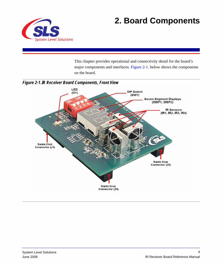
This chapter provides operational and connectivity detail for the board’s major components and interfaces. Figure 2-1. below shows the components on the board.
Figure 2-1. IR Receiver Board Components, Front View
4IR Receiver Board Reference Manual
System Level SolutionsJune 2008

Board Components
Table 2-1 lists the components on the IR Receiver board and the related interfaces.
IR Sensors The board contains 4 IR Sensors, which sense the IR signals transmitted by the IR transmitter. The board uses the TSOP1738 IR sensor which contains 3 pins and operates at 5 volts.
These sensors tune to the 38 KHz modulation frequency. PIN diode and preamplifier are assembled on the lead frame. The epoxy package is designed as IR filter. The IR filter gives demodulated output and this output signal can directly be given to the IR Receiver IP core inside the FPGA. Each sensor’s directivity is 90 degree because of which four IR sensor senses the IR signal from omnidirections.
Table 2-1. IR Receiver Board Components & Interfaces
Board Reference Name Description PageFeatured Device
IR1, IR2, IR3, IR4 IR Sensors Used to sense the IR signals transmitted by the IR transmitter
5
User Interfaces
Disp1, Disp2 Seven Segment Display Used for displaying the character 7
D1 User Defined LED Used for monitoring sensor output 8
SW1 DIP Switch Used for external input 9
Santa Cruz Connectors
J1, J2, J3 Santa Cruz Connectors Female connectors used for mount-ing board (In this case it is IR Board) on the Development Kit having stan-dard Santa Cruz short expansion male interface.
10
5IR Receiver Board Reference Manual
System Level SolutionsJune 2008

IR Sensors
Table 2-2 displays IR Sensor signals with its type & functionality.
Figure 2-2. shows the IR sensors in the board schematic.
Figure 2-2. Schematic view of IR Sensors
Table 2-2. IR Sensors Pin Table
IR SensorPin No.
Pin Name Type Description
1 VCC VCC +5 V Supply
2 GND GND Ground signal
3 VOUT Out Sensor Output (Active Low)
6 System Level SolutionsJune 2008IR Receiver Board Reference Manual

Board Components
Table 2-3 shows the mapping of IR Sensor pins with header.
Seven Segment Display
The board includes two Seven Segment Displays which are used to display data.
Figure 2-3. shows the seven segment display in the board schematic.
Figure 2-3. Schematic view of Seven Segment Display
Table 2-3. IR Sensors Pin Mapping
IR Sensor Pin No. IR Sensor Signal Name Header(F) Pin No.IR1.3 IR_OUT1 JP2.37
IR2.3 IR_OUT2 JP2.39
IR3.3 IR_OUT3 JP2.33
IR4.3 IR_OUT4 JP2.35
7IR Receiver Board Reference Manual
System Level SolutionsJune 2008

User Defined LED
Table 2-4 shows the mapping of Seven Segment Display pins with header.
User Defined LED
The board is provided with one user defined LED. This LED is mounted on the board with the purpose of monitoring sensor output. It can also be used for other purposes. Table 2-5 shows the mapping of User Defined LED with header.
Figure 2-4. shows the user defined LED in the board schematic.
Table 2-4. Seven Segments Display Pin Mapping
Seven Segment Display Pin No.
Seven Segment Display Signal Name
Header (F) Pin No.
DISP1.10 Segment_A1 JP2.17
DISP1.9 Segment_B1 JP2.15
DISP1.8 Segment_C1 JP2.13
DISP1.5 Segment_D1 JP2.3
DISP1.4 Segment_E1 JP2.5
DISP1.2 Segment_F1 JP2.9
DISP1.3 Segment_G1 JP2.7
DISP1.7 Segment_DP1 JP2.11
DISP2.10 Segment_A2 JP2.27
DISP2.9 Segment_B2 JP2.25
DISP2.8 Segment_C2 JP2.29
DISP2.5 Segment_D2 JP1.13
DISP2.4 Segment_E2 JP1.11
DISP2.2 Segment_F2 JP2.21
DISP2.3 Segment_G2 JP2.23
DISP2.7 Segment_DP2 JP2.31
Table 2-5. User Defined LED Pin Mapping
User Defined LED Pin No.
User Defined LED Signal Name
Header(F) Pin No.
D1 user_led JP2.28
8 System Level SolutionsJune 2008IR Receiver Board Reference Manual

Board Components
Figure 2-4. Schematic view of user defined LED
DIP Switch The board includes a 4-way DIP Switch, which can be used to provide external input.
Figure 2-5. shows the DIP switch in the board schematic.
Figure 2-5. Schematic View of DIP switch
Table 2-6 shows the mapping of DIP Switch pins with header.
Table 2-6. DIP Switch Pin Mapping
DIP Switch Pin No. DIP Switch Signal Name
Header(F) Pin No.
SW1.1 DIP_SW_1 JP1.8
SW1.2 DIP_SW_2 JP1.10
SW1.3 DIP_SW_3 JP1.12
SW1.4 DIP_SW_4 JP1.14
9IR Receiver Board Reference Manual
System Level SolutionsJune 2008

Santa Cruz Connector
Santa Cruz Connector
The board provides Santa Cruz Connector as shown in Figure 2-1. Using the three (Female) Santa Cruz Connector (J1, J3, J2), the board snaps on any development board having Santa Cruz Expansion Header.
Figure 2-6. shows the Santa Cruz Connector in the board schematic.
Figure 2-6. Schematic view of Santa Cruz Connector
10 System Level SolutionsJune 2008IR Receiver Board Reference Manual

Board Components
Figure 2-7. shows the Santa Cruz Connector - J1, J2, J3 pin description.
Figure 2-7. Santa Cruz Connector (F) - J1, J2, J3
1 2
3 4
5
7
9
12
1413
11
NC
Segment_D1
Segment_E1
Segment_G1
Segment_F1
Segment_DP1
Segment_C1
6
8
10
GND
NC
NC
NC
NC
NC
NC
19GND
17Segment_A1
15Segment_B1 16
18
20 NC
NC
NC
Segment_F2
Segment_C2
Segment_A2
Segment_G2
Segment_B2
IR_OUT4
IR_OUT3
Segment_DP2
IR_OUT2
IR_OUT1
21
23
25
27
31
29
37
35
33
39
22
24
32
34
26
28
30
36
38
40
GND
GND
GND
user_led
GND
NC
NC
NC
NC
GND
1 2
3 4
5
7
9
12
1413
11
NC
NC
+3.3 V
+3.3 V
NC
NC
NC
6
8
10
GND
GND
GND
GND
GND
GND
GND
19NC
17NC
15NC 16
18
20 GND
GND
GND
1 2
3 4
5
7
9
12
1413
11
GND
NC
NC
NC
NC
Segment_E
Segment_D
6
8
10
5V
NC
NC
DIP_SW_1
DIP_SW_2
DIP_SW_3
DIP_SW_4
J2 J1
J3
11IR Receiver Board Reference Manual
System Level SolutionsJune 2008

3. Signal Mapping (Board Specific)
This chapter provides IR Receiver Board’s components pin mapping table in order to use the board with UP3 1C6, DE1, DE2 Board.
IR Sensors Table 3-1 shows the IR Sensors pin mapping information with UP3 1C6, DE1, DE2 Board.
Seven Segment Display
Table 3-2 shows the Seven Segment Display pin mapping information with UP3 1C6, DE1, DE2 Board.
Table 3-1. IR Sensors Pin Mapping (Board Specific)
IR Sensor Pin No.
IR Sensor Signal Name
UP3 FPGA Pin No.
DE1 FPGA Pin No.
DE2 FPGA Pin No.
IR1.3 IR_OUT1 PIN_174 PIN_H18 PIN_U21
IR2.3 IR_OUT2 PIN_173 PIN_N21 PIN_V25
IR3.3 IR_OUT3 PIN_203 PIN_H17 PIN_R19
IR4.3 IR_OUT4 PIN_176 PIN_G17 PIN_T19
Table 3-2. Seven Segments Display Pin Mapping (Board Specific)
Seven Segment Display Pin No.
Seven Segment Display Signal Name
UP3 FPGA Pin No.
DE1 FPGA Pin No.
DE2 FPGA Pin No.
Segment_A1 Segment_A1 PIN_214 PIN_C19 PIN_T23
Segment_B1 Segment_B1 PIN_213 PIN_F20 PIN_T20
Segment_C1 Segment_C1 PIN_208 PIN_D14 PIN_P24
Segment_D1 Segment_D1 PIN_217 PIN_H13 PIN_K26
Segment_E1 Segment_E1 PIN_216 PIN_G15 PIN_M23
Segment_F1 Segment_F1 PIN_206 PIN_G16 PIN_M21
Segment_G1 Segment_G1 PIN_215 PIN_E15 PIN_M20
Segment_DP1 Segment_DP1 PIN_207 PIN_F13 PIN_M25
12IR Receiver Board Reference Manual
System Level SolutionsJune 2008

Signal Mapping (Board Specific)
User Defined LED
Table 3-3 shows the User Defined LED pin mapping information with UP3 1C6, DE1, DE2 Board.
DIP Switch Table 3-4 shows the DIP Switch pin mapping information with UP3 1C6, DE1, DE2 Board.
DISP2.10 Segment_A2 PIN_202 PIN_F20 PIN_T20
DISP2.9 Segment_B2 PIN_201 PIN_E20 PIN_T21
DISP2.8 Segment_C2 PIN_205 PIN_E18 PIN_U25
DISP2.5 Segment_D2 PIN_187 PIN_B17 PIN_F26
DISP2.4 Segment_E2 PIN_188 PIN_B16 PIN_J20
DISP2.2 Segment_F2 PIN_199 PIN_D19 PIN_T25
DISP2.3 Segment_G2 PIN_200 PIN_D20 PIN_T18
DISP2.7 Segment_DP2 PIN_204 PIN_G20 PIN_U23
Table 3-2. Seven Segments Display Pin Mapping (Board Specific)
Seven Segment Display Pin No.
Seven Segment Display Signal Name
UP3 FPGA Pin No.
DE1 FPGA Pin No.
DE2 FPGA Pin No.
Table 3-3. User Defined LED Pin Mapping (Board Specific)
User Defined LED Pin No.
User Defined LED Signal Name
UP3 FPGA Pin No.
DE1 FPGA Pin No.
DE2 FPGA Pin No.
D1 user_led PIN_196 PIN_E19 PIN_U26
Table 3-4. DIP Switch Pin Mapping (Board Specific)
DIP Switch Pin No.
DIP Switch Signal Name
UP3 FPGA Pin No.
DE1 FPGA Pin No.
DE2 FPGA Pin No.
SW1.1 DIP_SW_1 PIN_184 PIN_A15 PIN_F24
SW1.2 DIP_SW_2 PIN_183 PIN_A16 PIN_J21
SW1.3 DIP_SW_3 PIN_182 PIN_A17 PIN_F25
SW1.4 DIP_SW_4 PIN_198 PIN_A18 PIN_N18
13IR Receiver Board Reference Manual
System Level SolutionsJune 2008

This document is prepared as per the new revision of the IR Receiver Board (PCB-SBIR-076-B02). For users having the previous version of the board, please contact [email protected] specifying the number on the PCB for any queries.
14 System Level SolutionsJune 2008IR Receiver Board Reference Manual
Signal Mapping (Board Specific)
15IR Receiver Board Reference Manual
System Level SolutionsJune 2008

Appendix A. Signal Mapping (Board Specific)
The IR Keyboard along with the IR Receiver IP Core is provided as a deliverable with the SLS IR Receiver board that snaps on Altera standard Santa Cruz header. To create your Nios II application using the IR keyboard, you require the information about the codes that the keyboard sends out at every key press. This document provides you the information about the key codes of the IR Keyboard.
The Figure A-1. below shows the picture of IR Receiver board and the IR Keyboard.
Figure A-1. IR Keyboard with IR Receiver Board
Keys on IR Keyboard
The IR Keyboard does not follow the PS/2 protocol. It sends some code to the IR Receiver which is decoded by the IR Receiver IP core and sent to Nios which is to be controlled by the ‘C’ application. Therefore, at the end, the user has to handle an 8 digit key code. The table below lists the key codes for dif-ferent keys on the IR keyboard.
Table A-1. IR Keyboard Key Codes
Key Key Code Key Key Code Key Key CodeEsc 01011110 W 01000001 , or < 00110011
16IR Receiver Board Reference Manual
System Level SolutionsJune 2008

F1 01100010 E 00000001 . or > 01010011
F2 00100010 R 01110001 / or ? 00010011
F3 01000010 T 00110001 R. Shift 00101011
F4 00000010 Y 01010001 Ctrl 01000000
F5 01110010 U 00010001 Alt 01001011
F6 00110010 I 01101001 Home(sym) 01011100
F7 01010010 O 00101001 Num 01111011
F8 00010010 P 01001001 Space 00111011
F9 01101010 [ or { 00001001 Delete 01101000
F10 00101010 ] or } 01111001 Insert 01111100
F11 01001010 \ or | 00111001 Page Left 00110100
F12 00001010 Caps Lock 01011001 Key Up 00000000
Print 01001000 A 00011001 Page Right 01101100
Num Lock 01111010 S 01100111 Key Left 00011100
Scroll Lock 00111010 D 00100111 Key Down 01110000
Pause/Break 01011010 F 01000111 Key Right 00101000
` or ~ 00100101 G 00000111 Home 01100000
1 or ! 01000101 H 01110111 Page Up 00110000
2 or @ 00000101 J 00110111 Page Down 01010000
3 or # 01110101 K 01010111 End 00100000
4 or $ 00110101 L 00010111 Sm. Button 00011110
5 or % 01010101 ; or : 01101111 Big Button 00001110
6 or ^ 00010101 ‘ or “ 00101111 Black 01000100
7 or & 01101101 Enter 00001111 Green 00000100
8 or * 00101101 L. Shift 01111111 Parrot 00100100
9 or ( 01001101 Z 01011111 Blue 01110100
0 or ) 00001101 X 00011111 Red 01101011
- or _ 01111101 C 01100011 Violet 00011011
= or + 00111101 V 00100011 Sky 00010100
Table A-1. IR Keyboard Key Codes
17IR Receiver Board Reference Manual
System Level SolutionsJune 2008
IR Keyboard Joystick
IR Keyboard Joystick
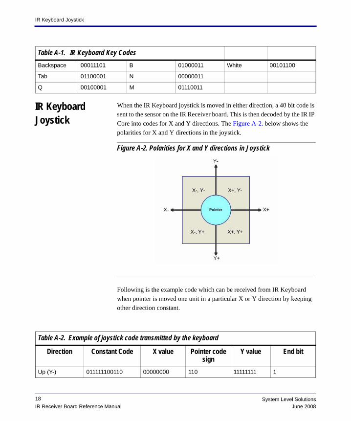
When the IR Keyboard joystick is moved in either direction, a 40 bit code is sent to the sensor on the IR Receiver board. This is then decoded by the IR IP Core into codes for X and Y directions. The Figure A-2. below shows the polarities for X and Y directions in the joystick.
Figure A-2. Polarities for X and Y directions in Joystick
Following is the example code which can be received from IR Keyboard when pointer is moved one unit in a particular X or Y direction by keeping other direction constant.
Backspace 00011101 B 01000011 White 00101100
Tab 01100001 N 00000011
Q 00100001 M 01110011
Table A-1. IR Keyboard Key Codes
Table A-2. Example of joystick code transmitted by the keyboard
Direction Constant Code X value Pointer code sign
Y value End bit
Up (Y-) 011111100110 00000000 110 11111111 1
18 System Level SolutionsJune 2008IR Receiver Board Reference Manual

Now to design your system with DE1, refer the tutorial “Designing IR System from Scratch for DE1” and to design your system with DE2, refer the tutorial “Designing IR Receiver System from Scratch for DE2”.
for getting started with IR Receiver board refer “IR Receiver Board Quick Start Guide”.
Down (Y+) 011111100110 00000000 110 10000000 1
Left (X-) 011111100110 11111111 110 00000000 1
Right (X+) 011111100110 10000000 110 00000000 1
Table A-2. Example of joystick code transmitted by the keyboard
19IR Receiver Board Reference Manual
System Level SolutionsJune 2008

IR Keyboard Joystick
20 System Level SolutionsJune 2008IR Receiver Board Reference Manual