irradiation characterization of eee components for space … · 2018-11-21 · the european space...
TRANSCRIPT

THE EUROPEAN SPACE AGENCY
Irradiation characterization of EEE components for space application
Michele Muschitiello, Ali Zadeh, Alessandra Costantino, Radiation Hardness Assurance and Components Analysis Section (TEC-QEC)ESA-ESTEC
RADSAGA Initial Training Event5 October 2017, Geneva
RADECS 2017 - CERN Geneva RADSAGA Initial Training Event 1

Space environment
RADSAGA Initial Training Event 2RADECS 2017 - CERN Geneva
Solar flares
• Protons (1keV - 500 MeV)
• Ions (1 – 10 MeV/n)
Cosmic rays
• Ions (up to 300MeV/n)
SOHO – Nov 2003
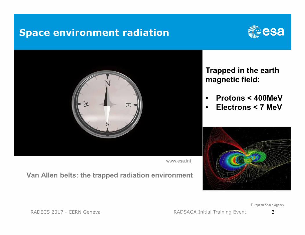
Van Allen belts: the trapped radiation environment
Space environment radiation
RADSAGA Initial Training EventRADECS 2017 - CERN Geneva
Trapped in the earth
magnetic field:
• Protons < 400MeV
• Electrons < 7 MeV
www.esa.int
3

The effects of radiation on electronic devices and materials depend on :- Type of radiation (photon, electron, proton...)- Rate of interaction - Type of material (Silicon, GaAs..)- Component characteristics (process, structure, etc.)
RADSAGA Initial Training EventRADECS 2017 - CERN Geneva
Interaction of Radiation Particles with Electronic Devices and Materials
Interaction mechanisms :
- Ionization - Internal Charging- Displacement Damage
Consequences :
- Performance Degradation - Transient errors/malfunctions- Permanent Damages
4

Radiation Hardness Assurance for Space
RADSAGA Initial Training EventRADECS 2017 - CERN Geneva
Radiation hardness assurance methodology is followed to ensure that the radiation environment does not compromise the functionality and performances of electronics during the system life.
ECSS European Cooperation for Space StandardizationESCC European Space Components Coordination (escies.org)
RHA: ECSS-Q-ST-60-15C, ECSS-E-ST-10-12C, ECSS-E-HB-10-12, ECSS-Q-HB-60-02A
TID : ESCC 22900 SEE: ESCC 25100
http://ecss.nl/
5

Radiation Hardness Assurance for Space
RADSAGA Initial Training EventRADECS 2017 - CERN Geneva
Radiation Hardness Assurance (RHA) deals with:
• system requirements, • space environment definition, • radiation tolerant design,• part selection, • part testing, • shielding• etc…
6

Cumulative effect result of particle energy
deposition in the bulk of the semiconductor. It is
also referred to as Total Non-ionizing Dose
(TNID) damage
Main radiation effects in Electronic component materials
RADSAGA Initial Training EventRADECS 2017 - CERN Geneva
Interstitials
Vacancies
Oxide
Silicon
p+ (e-)
Displacement Damage (DD)
+ + + + + + + + +
+ - - + - + - + - - -Oxide
Silicon
Trapped
charges
Interface
traps
p+e-
Total Ionising Dose (TID)
Ion
Ionisation
+ - +
- + + -
+ - - +
-+ + +
Oxide
Silicon
p+
Ion 2nd
Single Event Effects (SEE)
The creation of electron-holes pair in the material
cause long term effects in the oxide (charge
trapping) and at oxide-semiconductor interface
(interface states)
Ionization is created by direct energy deposition along ion tracks
or the energy is deposited by fragments of nuclei from
inelastic collision between a proton and a lattice nucleus.
The fragments usually deposit in turn all their energy along
their track or produce a cascade of secondary particles.
7
8
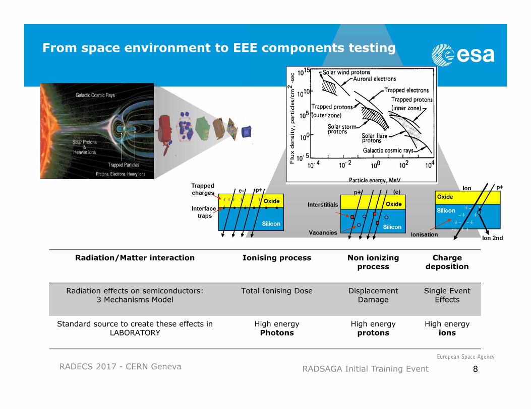
Radiation/Matter interaction Ionising process Non ionizing process
Charge deposition
Radiation effects on semiconductors:3 Mechanisms Model
Total Ionising Dose Displacement Damage
Single Event Effects
Standard source to create these effects in LABORATORY
High energyPhotons
High energy protons
High energy ions
From space environment to EEE components testing
RADECS 2017 - CERN Geneva RADSAGA Initial Training Event

9
Total Ionising Dose Displacement Damage Single Event Effects
Cumulative effect:Gradual global degradation of device parameter
Probabilistic effect:transient, permanent or static errors.
PERFORMANCE DEGRADATIONas function of :
CROSS SECTION (=Probability of SEE occurrence )
as function of:
Total dose [rad(Si)] [Gy(Si)] Fluence [p/cm2] Linear energy transfer [MeV/mg/cm2]
Other parameters:Dose rate [rad(Si)/s] [Gy(Si)]
Other irradiation test parameter: Proton Energy [MeV],
Flux [p/cm2/s]
Other irradiation test parameter: Flux[p/cm2/s] , particle range [um]
What to expect from testing
0
0.2
0.4
0.6
0.8
1
0 25 50 75 100 125
Norm
alized C
TR
Total Ionizing Dose (krad)
Isolink OLS449
Biased (If=1mA,Vce=5V) , 360 rad(Si)/h
GND , 360 rad(Si)/hBiased (If=1mA,Vce=5V) , 36 rad(Si)/h
GND , 36 rad(Si)/h
0
0.2
0.4
0.6
0.8
1
0 100 200
Annealing hours
RADECS 2017 - CERN Geneva RADSAGA Initial Training Event
TID testing
RADECS 2017 - CERN Geneva RADSAGA Initial Training Event 10

ESA 60Co facility for TID testing at ESTEC
RADSAGA Initial Training EventRADECS 2017 - CERN Geneva
ESA Co60 Facility
European Space and Technology
Research Center (ESTEC)
The Netherlands
Info on ESCIES :
https://escies.org/webdocument/showArticle?id=227&
groupid=6
Beamtime reservation and current schedule:
https://estecco60facility.esa.int/
The ESTEC GAMMABEAM 150C Co-60 facility was first installed in 1988 and has been in use ever since.
The source housing has collimated layout and allows DUTs to be exposed to different dose rates by varying their distance over a range up to 8 meters away from the source.
The initial activity at each reload is ~85 TBq with a half life of 5.3 years, the source has been re-loaded several times. The last reload was in May2016
ESA's Space Research and Technology Centre Noordwijk – The Netherlands
11

The 60Co facility – source characteristics
RADSAGA Initial Training EventRADECS 2017 - CERN Geneva
60Cocontainer
23.5 mm
36.5
mm
Nominal activity at reload: 85TBq
Advantages of using gammas:
• No material activation.• Irradiation in air• No de-lidding necessary
The 60Co isotope undergoes beta decay with a half-life of 5.272 years producing the nuclear excited state of 60Ni from which it emits either one or two gamma ray photons to reach the Nickel ground state.
- 60Co Decay products => photons 1.173 MeV, 1.332 MeV
- 60Co Half life =5.27 years
ESTECCo-60 source
container
12

The ESA-ESTEC 60Co facility
RADSAGA Initial Training EventRADECS 2017 - CERN Geneva 13

60Co facility – The control room
RADSAGA Initial Training EventRADECS 2017 - CERN Geneva
Recommended ~ 6m cable length to connect DUT in the irradiation room to equipment in the control room
Feedthough layout:
Operator area Equipment for DUT monitoring / characterization
14
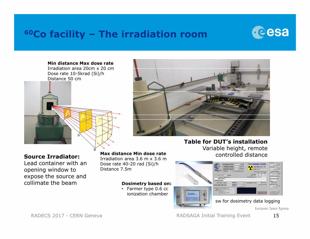
60Co facility – The irradiation room
RADSAGA Initial Training EventRADECS 2017 - CERN Geneva
Source Irradiator:Lead container with an opening window to expose the source and collimate the beam
Table for DUT’s installationVariable height, remote
controlled distance
Min distance Max dose rateIrradiation area 20cm x 20 cm Dose rate 10-5krad (Si)/hDistance 50 cm
Max distance Min dose rateIrradiation area 3.6 m x 3.6 m Dose rate 40-20 rad (Si)/hDistance 7.5m
Dosimetry based on:• Farmer type 0.6 cc
ionization chamber
sw for dosimetry data logging
15

60Co facility – Live footage
RADSAGA Initial Training EventRADECS 2017 - CERN Geneva 16

60Co facility – how to request beam time
RADSAGA Initial Training EventRADECS 2017 - CERN Geneva
1) Compile the on-line beamtime request formhttps://estecco60facility.esa.int
2) Send a Test plan for review and approval
17

Why using a Co60 source for TID testing
RADSAGA Initial Training EventRADECS 2017 - CERN Geneva
TID testing employing 60Co facilities (gamma source) has, over the years, become the de-facto standard test method.
This is due to the high yield of the Co60 gamma ray beam, long heritage of Co60 use in industry and medical application,
availability of the isotope…
• In some cases electrons, protons and x-rays are also used to perform TID testing.
• Care has to be shown when employing other sources than 60Co (range in the material, dosimetry …)
In space high energy photons are not a concern compared to the other sources of radiation. However, it has been empirically shown that 60Co testing is conservative compared to testing with protons or electrons.
JPL course by J.Conley
Fig: electron-hole pair generation (ionisation) yield in matter for various particle species, energy and field across oxide.
18

Some effects in MOS transistors:
• Gate voltage threshold shifts
• Leakage increases, flat band shift
• Channel resistivity increase
Caused by oxide and interface traps
Total Ionizing Dose (TID) effects
RADSAGA Initial Training EventRADECS 2017 - CERN Geneva
The total dose deposited by electrons or protons alters
the electrical characteristics of electronic components
In Bipolar transistors:
• leakage increase
• Reduction of the gain
• Noise figure worsening
A variety of factors influence the TID effects on the devices:
• Temperature• Electric fields over oxides (magnitude and polarity)• Dose rates• Technology• Process (including lot to lot variation)• Design rules• …
After Space Radiation Effects on Microelectronics course from JPL, J.F. Conley
19

20
TID Test preparation
SCOPE
The specification defines the basic requirements applicable to the steady-state irradiation testing of integrated circuits and discrete semiconductors suitable for space applications.
PURPOSE
1.The specification addresses three cases:
• The evaluation testing procedure: main objectives to establish worst case conditions for TID qualification (dose level, dose rate effects, bias dependency, critical parameters, annealing effects, etc..)
• the qualification and lot acceptance testing procedures: test conditions identified in the evaluation phase
• the testing outside ESCC context: no hard requirements in terms of sample size, dose rates, pass/fail criteria (can be project and/or application specific not just related to the datasheet).
1.ESCC22900
Other standards and references: • MIL-STD883 Method 1019.9 “Ionizing Radiation (Total Dose) Test Procedure”• MIL-STD750 Method 1019.5 “Steady-state Total Dose Irradiation Procedure”• ASTM F 1892-06 “Standard Guide for Ionizing Radiation (Total Dose) Effects Testing of Semiconductor”
ESCC Basic Specification 22900 : Total Dose Steady-State Irradiation Test Method
Specification -> https://escies.org/download/specdraftapppub?id=3413
Test plan template -> https://escies.org/download/webDocumentFile?id=62995
RADECS 2017 - CERN Geneva RADSAGA Initial Training Event

21RADSAGA Initial Training Event
ESTEC CO60
Absorbed dose (D)the mean energy imparted to matterper unit mass by ionizing radiation
The SI unit of measure is gray [Gy] 1Gy equals 1 joules per kilogram
The historical, and most used unit is [rad] 1 rad =100 Gy
The dose depends on the matter considered => specify dose in matter ( eg. rad(Si), Gy(SiO2)…)
Dose rate (DR = dD/dt)the quantity of radiation absorbed per unit time
TID Test: dose rate ranges comparison
RADECS 2017 - CERN Geneva

TID Test Flow
RADSAGA Initial Training EventRADECS 2017 - CERN Geneva
Irradiation testing is performed to
identify whether a component meets
specification/application requirements
when exposed to desired/application
radiation doses.
Initial Measurement
TID Irradiation
Interim Measurement
Annealing/aging atroom and high temperature
Final MeasurementData analysis
22

TID TEST RESULTS
RADECS 2017 - CERN Geneva RADSAGA Initial Training Event 23

Sp
ecif
icati
on
lim
it
TID effects - TEST CASE 1
RADSAGA Initial Training EventRADECS 2017 - CERN Geneva
Device under test: Low noise precision Operational Amplifier
100krad rad hard qualified has failed at 20krad(Si)
Why so far from qualification data?
a. dose rate – this test :~ 10mrad(Si) s-1 qualification: 50-300rad(Si) s-1
b. biasing condition – qualification requests only one biasing condition (V=+-15)
In this case the worst case is unbiased
Unbiased case is important for cold redundancy and off period during transfer orbit
Unbiased
Biased
reference
24

25
Ionizing Radiation induced charge trapping and interface state generation in MOS Structure
RADECS 2017 - CERN Geneva RADSAGA Initial Training Event
REFERENCE SAMPLE
-Setup measurement long term stability over time
- Environmental effects
- Setup functionality
- Statistical contribution to uncertainty
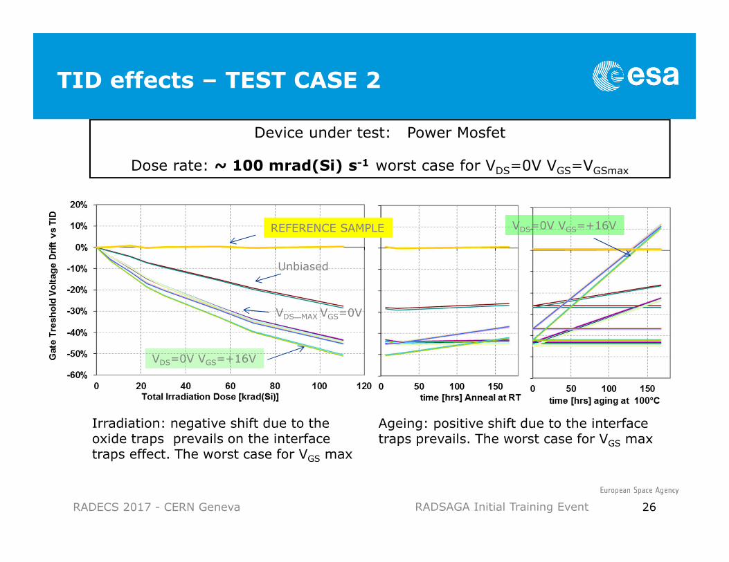
TID effects – TEST CASE 2
RADSAGA Initial Training EventRADECS 2017 - CERN Geneva
VDS=0V VGS=+16V
Unbiased
VDS_MAX VGS=0V
VDS=0V VGS=+16VREFERENCE SAMPLE
Device under test: Power Mosfet
Dose rate: ~ 100 mrad(Si) s-1 worst case for VDS=0V VGS=VGSmax
26
Irradiation: negative shift due to the oxide traps prevails on the interface traps effect. The worst case for VGS max
Ageing: positive shift due to the interface traps prevails. The worst case for VGS max
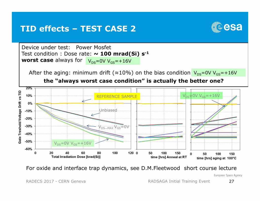
TID effects – TEST CASE 2
RADSAGA Initial Training EventRADECS 2017 - CERN Geneva
VDS=0V VGS=+16V
Unbiased
VDS_MAX VGS=0V
VDS=0V VGS=+16VREFERENCE SAMPLE
Device under test: Power MosfetTest condition : Dose rate: ~ 100 mrad(Si) s-1
worst case always for
After the aging: minimum drift (≈10%) on the bias condition
the “always worst case condition” is actually the better one?
For oxide and interface trap dynamics, see D.M.Fleetwood short course lecture
27
VDS=0V VGS=+16V
VDS=0V VGS=+16V

TID effects – TEST CASE 3
RADSAGA Initial Training EventRADECS 2017 - CERN Geneva
Device under test: MOSFET
Result: at the end of the test static parameters seems still “OK”
Ref: MIL STD 750 method 3471
After room temp anneal
After hightemp anneal
Initial
After 100krad
However, the charge needed to
switch on/off the MOSFET is
about 30% higher than the initial
value.
The MOSFET switching
characteristics will be significantly
degraded!
28

TID effects – TEST CASE 3
RADSAGA Initial Training EventRADECS 2017 - CERN Geneva
(www.vishay.com AN608A)
Device under test: MOSFET
Result: at the end of the test, the trapped charges at the interface will still affect
the switching characteristic of the MOSFET
29

TID effects – to keep in mind
RADSAGA Initial Training EventRADECS 2017 - CERN Geneva
• TID predominantly affects the device oxide resulting in device parameter
degradation
• Co-60 gamma ray most common used radiation source
• Sensitivity to TID is strongly technology and manufacturing process
dependent.
• ELDRS can be an issue for bipolar based devices
• Lot-non-uniformity is an issue for TID specifically with respect to Enhanced
Low Dose Rate Sensitivity (ELDRS) issue
• New Deep Sub Micron (DSM) technologies seem quite TID tolerant…
... keep testing! (see D.M. Fleetwood, RADECS 2017 short course)
30
The Displacement Damage is not an oxide effect but is a result of
the particle energy deposition in the bulk of the material that
creates defects in the semiconductor lattice.
As for TID, DD (or TNID) is a cumulative effect and produces
parametric degradation of the device performances.
DD testing
The ECSS-E-HB-10-12A standards provide detailed guidelinesFor DD testing of electronic devices.
RADECS 2017 - CERN Geneva RADSAGA Initial Training Event 31

Displacement Damage – some effects
RADSAGA Initial Training EventRADECS 2017 - CERN Geneva
Technology category sub-category Effects
General bipolar BJT hFE degradation in BJTs, particularly for low-current conditions (PNP devices more sensitive to DD than NPN)
diodes Increased leakage current
increased forward voltage drop
Electro-optic sensors CCDs CTE degradation, Increased dark current, Increased hot spots, Increased bright columns
Random telegraph signals
APS Increased dark current, Increased hot spots, Random telegraph signals
Reduced responsivity
Photo diodes Reduced photocurrents
Increased dark currents
Photo transistors hFE degradation
Reduced responsivity
Increased dark currents
Light-emitting diodes LEDs (general) Reduced light power output
Laser diodes Reduced light power output
Increased threshold current
Opto-couplers Reduced current transfer ratio
Solar cells Silicon
GaAs, InP etc
Reduced short-circuit current
Reduced open-circuit voltage
Reduced maximum power
Optical materials Alkali halides
Silica
Reduced transmission
see the ECSS-E-HB-10-12A standard, paragraph 7 for more details
32

SEE testing
RADECS 2017 - CERN Geneva RADSAGA Initial Training Event 33
Single Event Effect (SEE)basic mechanism
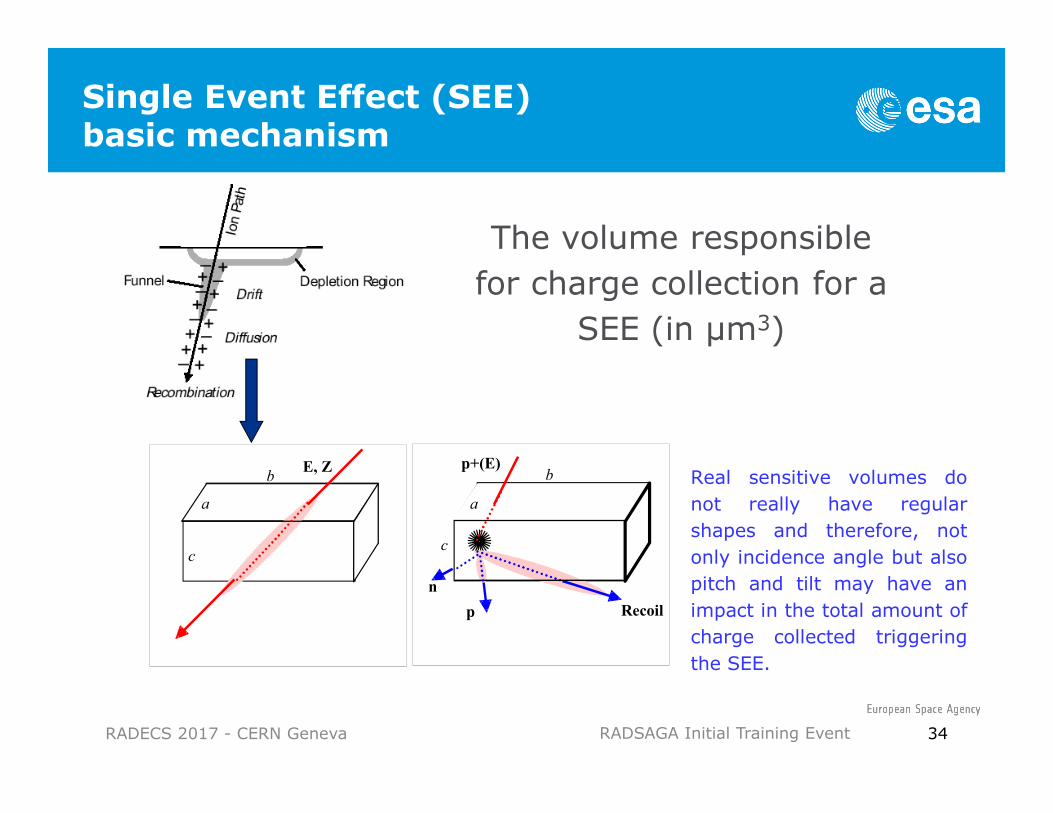
RADSAGA Initial Training EventRADECS 2017 - CERN Geneva
The volume responsible
for charge collection for a
SEE (in μm3)
E, Z
a
b
c
p+(E)
Recoilp
n
a
b
c
Real sensitive volumes do
not really have regular
shapes and therefore, not
only incidence angle but also
pitch and tilt may have an
impact in the total amount of
charge collected triggering
the SEE.
34
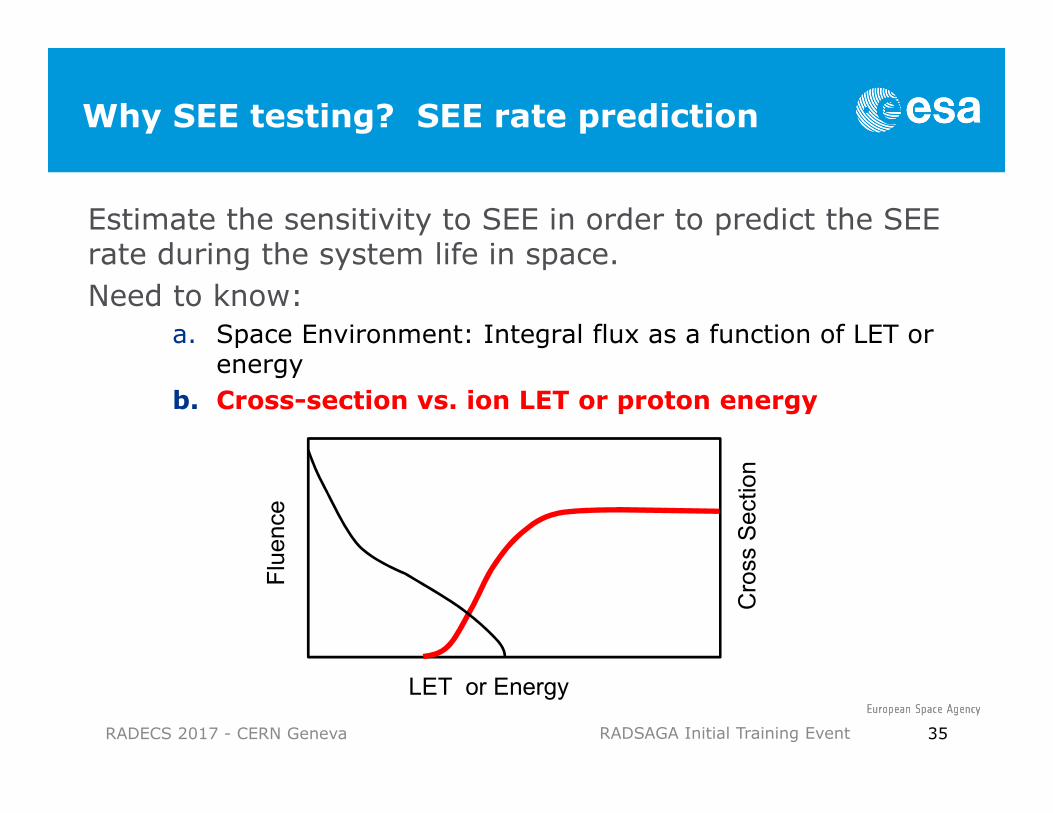
Why SEE testing? SEE rate prediction
RADSAGA Initial Training EventRADECS 2017 - CERN Geneva
Estimate the sensitivity to SEE in order to predict the SEE rate during the system life in space.
Need to know:
a. Space Environment: Integral flux as a function of LET or energy
b. Cross-section vs. ion LET or proton energy
Cro
ss S
ection
Flu
ence
LET or Energy
35

SEE Cross Section Curve vs LET
RADSAGA Initial Training EventRADECS 2017 - CERN Geneva
The SEE cross section measures the probability for a SEE to occur
Fit with Weibull (integral form)
SEE cross-section is a crucial input for in-orbit SEE rate prediction.
0 10 20 30 40 50 60
LET (MeV.cm²/mg)
SE
E C
ross
sec
tio
n (
cm²)
LETth
σsat
W and S are fitting parameters
−−=
S
thsat
W
LETLETexp1σσ
[Nparticles/cm2][cm2]
Fluence
Nσ events=
ESCC 25100 Single Event Effects Test Method and Guideline
36

Some classes of SEE
RADSAGA Initial Training EventRADECS 2017 - CERN Geneva
Soft Errors (no permanent damage)
• SEU Single-Event Upset
• MBU, MCU Multiple Bit (or Cell) Upset
• ASET Analog Single Event Transient
• DSET Digital Single Event Transient
• SEFI Single Event Functional Interrupt
• (*) Others…
Hard Errors (permanent damage of device)
• SEL Single-Event Latchup (non destructive test still possible…)
• SEDR Single-Event Dielectric Rupture
• SEB Single-Event Burnout
• SEGR Single-Event Gate Rupture
• (*) Others...
When possible, identifythe Safe operating area}
(*) the one that always occurs
when you do not expect it !
37

SEE testing – TEST CASE 4Safe Operation Area (SEGR - SEB)
RADSAGA Initial Training EventRADECS 2017 - CERN Geneva
Nominal Device characteristics:• VDSmax= +60V• VGSmax= ±20V
Application requirements:• 0V ≤ VDS ≤+15V• 0V ≤ VGS ≤ +6V
The application requirements are appropriatesince they fall within the SOA
38
39
External irradiation test facilities – supported by
RADEF, JYFLJyväskylä, Finland
UCLLouvain-la-NeuveBelgium
PSIVilligenSwitzerland
Heavy ions, protons, electrons
Heavy ions, protons
Protons, electrons
ESA has been collaborating with the three external test facilities for more than 25-years.
Aiming at continuous improvement of the quality of the beam, dosimetry and testing infrastructure
( Stable flux and energy levels, high particle selectivity, accurate
dosimetry, electrical/optical interfaces for cabling…)
The support from the cooperative funding programmes has been crucial for the success of this collaboration.
The network has been supporting most of the space programs worldwide becoming a well established reference for the scientific and industrial community in the field of radiation effects on electronic components.
RADECS 2017 - CERN Geneva RADSAGA Initial Training Event

40
External Facilities factsheet
PSI(Switzerland)
RADEF (Finland) UCL(Belgium)
Proton Beam 74 - 200 MeV 0.5 - 52 MeV 14 - 62 MeV
Heavy ion beam 7.16 - 69.2MeV/cm2/s
1.3 - 62.5 MeV/cm2/s
RADECS 2017 - CERN Geneva RADSAGA Initial Training Event40

41
Practical aspects of Testing
TID test DD test SEE test
Source type Co60 gamma rays Proton Irradiation Heavy Ions Irradiation
Decay of radioactive source Particle accelerator (cyclotron) Particle accelerator (cyclotron)
Irradiation in Air Air Vacuum
Die need to be exposed? No No YES
Activation of irradiated DUT? No YES NO
Test duration Days / Weeks Some hours (8 h) Some hours (8 h)
Irradiation execution Irradiation 24/7Access to the facility: office hours
Irradiation in shifts (24/7)Typically 8/12h
Irradiation in shifts (24/7)Typically 8/12h
How in advance to book 1 Month 3 Months 3 Months
Beam sharingYes (up to 3 tests at different dose rates)
No No
Beam diameter From 20 cm to 3 m Approx 8 cm Approx 3 cm
Cable length from control to DUT 6 m 10-20 m 3m
€ €€€ €€€
RADECS 2017 - CERN Geneva RADSAGA Initial Training Event

What we would like to achieve when we do testing ?
RADSAGA Initial Training EventRADECS 2017 - CERN Geneva
… just do our best to have satellites performing “simple tasks” in space
according to the plan… after 12 years from the launch.
42
Thank you !
RADSAGA Initial Training EventRADECS 2017 - CERN Geneva
http://www.esa.int/About_Us/Careers_at_ESA
Undergraduate programsStages
Graduate programsYoung Graduate Training
PhD programsNetworking Partner Initiative
Staff positionsContractor positions
43