is 12032-12 (1994): graphical symbols for diagrams in the ... · certain terminology and...
TRANSCRIPT

Disclosure to Promote the Right To Information
Whereas the Parliament of India has set out to provide a practical regime of right to information for citizens to secure access to information under the control of public authorities, in order to promote transparency and accountability in the working of every public authority, and whereas the attached publication of the Bureau of Indian Standards is of particular interest to the public, particularly disadvantaged communities and those engaged in the pursuit of education and knowledge, the attached public safety standard is made available to promote the timely dissemination of this information in an accurate manner to the public.
इंटरनेट मानक
“!ान $ एक न' भारत का +नम-ण”Satyanarayan Gangaram Pitroda
“Invent a New India Using Knowledge”
“प0रा1 को छोड न' 5 तरफ”Jawaharlal Nehru
“Step Out From the Old to the New”
“जान1 का अ+धकार, जी1 का अ+धकार”Mazdoor Kisan Shakti Sangathan
“The Right to Information, The Right to Live”
“!ान एक ऐसा खजाना > जो कभी च0राया नहB जा सकता है”Bhartṛhari—Nītiśatakam
“Knowledge is such a treasure which cannot be stolen”
“Invent a New India Using Knowledge”
है”ह”ह
IS 12032-12 (1994): Graphical symbols for diagrams in thefield of electrotechnology, Part 12: Binary logic elements[LITD 5: Semiconductor and Other Electronic Components andDevices]


IS 12032 ( Part 12 ) : 1994 IEC Pub 617-12 (1983)
CONTENTS
PW . 3
. . 5
. 5
. . 5
. 5
NATIONALFOREWORD.. .......................................
CI~AP~RI : GENERAL ......................................
Section 1 - Introduction ..........................
Section 2 - General notes ........................
Section 3 - Explanation of terms ...................
. . . . . . . . . . . . . . . . . . . . . . . . .
. .
. . . . . . . . . . . . . . . . . . . .
. .
. . . . . . . . . . . . . . ...*.. . . * . .
. .
CHAPTER II : SYMBOL CONSTRUC-IION .............................
Section 4 - Composition of the symbol ..............
Section 5 - Outlines . : ...........................
Section 6 - Use and combination of outlines .........
. . . . .
. .
. . .
. .
. . . . . . . . . . . . 7
. 7
. . . 8
. . . . 8
. .
. . . . . . .
. . . . . .
CHAPTER II I : Q~ALIFWNG SYM~(OLS ASSOCIATED wmc INPUIS. oumrls AND OTHER CONNFUIONS .
Section 7 - Negation, logic polarity and dynamic input ..............
Section 8 - Internal connections ................................
Section 9 - Symbols inside the outline .................... , ......
Section 10 - Non-logic connections and signal-flow indicators ........
...... 13
...... 13
...... 14
...... 1.5
...... 26
. . . .
. . . . . . .
. . . . . .
. . . .
&XPTER iv : DEPENDENCY NOTATlON ..................................................
Section 11 - General explanation ...................
Section 12 - Cnnvention .......................... .
. . 27
. . . . 27
. 27
. 29
29
30
31
. 32
33
. . . . 34
. 36
. . 37
. 38
39
42
44
.
Section13-Typesofdependency ......................................
Section 14 - AND dependency (C-dependency) ...........................
Section 15 - OR dependency (V-dependency) .............................
Section 16 - NEGATE dependency (N-dependency) ........................
Section 17 - INTERCONNECTION dependency (Z-dependency) .............
Section 18- CONTROLdependency(C-dependency) ......................
Section 19 - SET and RESET dependency (S- and R-dependency) .............
Section 20 - ENABLE dependency (En-dependency) .......................
Section 21 - MODE dependency (M-dependency) .........................
Section 22 - Comparison of C-, EN- and M-effects on inputs .................
Section 23 - ADDRESS dependency (A-dependency) .......................
Section 24 - Special techniques used in dependency notation .................
Section 25 - The ordering of labels associated with inputs and with outputs .....
.
. . .
. .
.
. .
.
. .
.
.
CHAPTER v : C’OMBINA’“VEANDSEQuENTIAL ELEMENTS . . . . . . . , ,
Section 26 - General notes . . . . . . . .
Section 27 - Combinative elements . .
Section 28 - Examples of combinative elements .
Section 29 - Examples of buffets, drivers and receivers
Section 30 - Elements with hysteresis . .
Section 31 - Examples of elements with hysteresis
Section 32 - Coders, code converters . .
. . . . . 48
48
. . . . 48
50
54
. . 57
. 57
. . 58
. . .
. .
. .
. . .
. .
. . . .
1

IS 12032 ( Part 12 ) : 1994 J,EC Pub 617-12 ( 1983 )
Section 33 - Examples of code converters .......................... . . . . . . . . . . 60
Section 34 - Signal-level converters with or without galvanicseparation . . . . . . . . . 64
Section 35 - Examples of signal-level converters ..................... . . . . . . . . . . . 64
Section 36 - Multiplexers and demultiplexers ....................... . . . . . . . . . . . . 64
Section 37 - Examples of multiplexers and demultiplexers ............. . . . . . . . . . . . . . 65
Section 38 - Arithmetic elements ................................. . . . . . . . . . . . . * 67
Section 39 - Examples of arithmetic elements ....................... . . . . . . . . . . . 69
Section 40 - Binary delay elements ................................ . . . . . . . 73
Section 41 - Bistable elements ................................... . . . . . . . . . . 74
Section 42 - Examples of bistable elements ......................... . . . . . . . . . . 75
Section 43 - Indication of special switching properties of histable elements . . . . . . . . 78
Section 44 - Monostable elements ................................ . . . . . . . . . . . . . 78
Section 45 - Examples of monostable elements ...................... . . . . . . 79
Section 46 - Astable elements ............................................................ 79
Section 47 - Examples of astable elements .................................................. 81
Section 48 - Shift registers and counters .................................................... 82
Section 49 - Examples of shift registers and counters ......................................... 82
Section SO- Memories ................................................................. 88
Section 51 - Examples oC memories ....................................................... 89
I
2

IS 12032 ( Part 12 ) : 1994 IEC Pub 617-12 ( 1983 )
Indian Standard
GRAPHICALSYMBOLSFORDIAGRAMSIN THEFIl$DOFELECTROTECHNOLOGY \~
PART 12 BINARY LOGIC ELEMENTS
NATIONAL FOREWORD
This Indian Standard (Part 12) which is identical with IEC Pub 617-12 (1983) ‘Graphical symbols for diagrams - Part 12 : Binary logic elements’, issued by the International Electrotechnical Commission (IEC) was adopted by the Bureau of Indian Standards on the recommendation of the Basic Standards, on Electronics and Telecommunication Sectional Committee (LTD 1) and approval of the Electronics and Telecommunication Division Council.
The text of IEC Standard has been approved as suitable for publication as Indian Standard without deviations. Certain terminology and conventions are, however, not identical with those used in Indian Standards. Attention is specially drawn to the following:
Wherever the words ‘International Standard’ appear, referring to this standard, they should be read as ‘Indian Standard’.
In the adopted standard ( normative ) references appear to certain International Standards for which Indian Standards also exist. The corresponding Indian Standards which are to be substituted in their place are listed below along with their degree of equivalence for the editions indicated:
International Standard
IEC Pub 117-15 ( 1972) Recommended graphical symbols -Part 15 : Binary logic elements
IEC Pub 617-l ( 1985 ) Graphical sym- bols for diagrams -Part 1 : General information, general index - Cross reference tables
IEC Pub 617-2 ( 1983 ) Graphical sym- bols for diagrams - Part 2 : Symbol elements, qualifying symbols and other symbols having general applications
IEC Pub 617-3 ( 1983 ) Graphical symbols for diagram - Part 3 : Conductors and connecting devices
IEC Pub 617-10 ( 1983 ) Graphical symbols for diagrams - Part 10 : Telecommunications and transmis- sion
IEC Pub 617-13 ( 1978 ) Graphical symbols for diagrams - Part 13 : Analogue elements
Indian Standard
IS 2032 ( Part 24 ) : 1980 Graphical symbols used in electrotechnology: Part 24 Binary logic elements
IS 12032 ( Part 1 ) : 1987 Graphical symbols for diagrams in the field of electrotechnology: Part 1 General in- formation
IS 12032 ( Part 2 ) : 1987 Graphical symbols for diagrams in the field of electrotechnology : Part 2 Symbol elements, qualifyingsymbolsand other symbols having general applications
IS 12032 ( Part 3 ) : 1987 Graphical symbols for diagrams in the field of electrotechnology : Part 3 Conductors and connecting devices
IS 12032 ( Part 10 ) : 1990 Graphikal symbols for diagrams in the field of electrotechnology : Part 10 Telecom- munications and transmission
IS 12032 ( Part 13 ) : 1990 Graphical symbols for diagrams in the field of electrotechnology : Part 13 Analogue elements
3
Degree of Correspondence
Technically equivalent
Identical
Identical
Identical
Identical
Identical

IS 12032 ( Pat-t 12 ) : 1994 IEC Pub 617-12 ( 1983 )
The Basic Standards on Electronics and Telecommunication Sectional Committee has reviewed the provisions of the following IEC Standard and has decided that it is acceptable for use in conjunction with this standard :
IEC Pub 113-7 ( 1981 ) Diagrams, charts, tables - Part 7 : Preparation of logic diagrams
This Indian Standard is the twelfth part of the series of Indian Standards on Graphical symbols for diagrams, other parts are :
Part 1 General information
Part 2 Symbol elements, qualifying symbols and other symbols having general application
Part 3 Conductors and connecting devices
Part 4 Passive components
Part 5 Semiconductors and electron tubes
Part 6 Production and conversion of electrical energy
Part 7 Switch gear, control gear and productive devices
Part 8 Measuring instruments, lamps and signalling devices
Part 9 Telecommunication; switching and peripheral equipment
Part 10 Telecommunications; transmission
Pai 11 Architectural and topographical installation plans and diagrams
Part 13 Analogue elements
Only the English language text in the International Standard has been retained while adopting it in this Indian Standard/
4

IS 12032 ( Part 12 ) : 1994 IEC Pub 617 - 12 ( 1983 )
Indian Standard
GRAPHICALSYMBOLSFORDIAGRAMSINTHE FIELDOFELECTROTECHNOLOGY
PART 12 BINARY LOGIC ELEMENTS
1.1
2.1
2.2
2.3
2.4
2.5
CHAPTER 1: GENERAL
SECTION 1 - INTRODUCTION
This standard contains graphical symbols which have been developed to represent logic functions. They are iIIteIIded also to represent physical devices capable of carrying out these functions. The symbols have been prepared with a view to electrical applications but the majority may also be applied to non-electrical devices, for exaInple pneumatic, hydraulic, Inechancial.
Sl%l-lON 2 - GENERAL NOTES
Symbols in accordance with the superseded IEC Publication 117-15: Recommended Graphical Symbols, Part 15 : Binary Logic Elements, will be required for a prolonged changeover period but should be progressively superseded by the symbols given in this standard. Although non-preferred, the use of other syInbols recognized by official national standards, i.e. distinctive shapes in place of symbols 12-27-01, 12-27-02, 12-27-09, 12-27-10, 12-27-11, 12-27-12, 12-28-01, 12-28-02 and 12-2X-04, shall not be considered to bc in coutmdictiou with this standard. Usage of these other
symbols in combiIIatioII to form complex syInbols (e.g. use as eInbedded symbols) is discouraged.
For explaoation of “logic states “, “logic levels”, etc., see IEC Publication 113-7: Diagrams, Charts,
Tables, Part 7 : Preparation of Logic Diagrams.
This standard uses the symbols 0 and 1 to identify the two logic states of a binary variable. These states are referred to as O-state and l-state.
A binary variable may be equated to any physical quautity for which two distinct nnges can be defined. ln this staudard these distiIIct ranges are referred to as logic levels and are denoted H and L.
H is used to denote the logic level with the more positive algebraic value, and L is used to denote the logic level with the less positive algebraic value.
III the case of system in which logic states are equated with other qualities of a physical quantity (e.g. positive or negative pulses, presence or absence of a pulse), H and L may be used to represent these qualities or may be replaced by Inorc suitable designations.
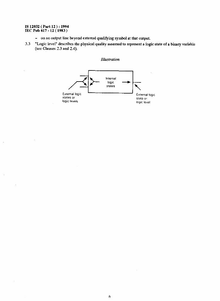
SECTION 3 - EXPLANATION OF TERMS
To facilitate understanding of the descriptions in the rest of this staudard, it is useful to dcfinc thrcr terms.
3.1 “Internal logic state” describes a logic state assumed to exist inside a symbol outline at iIIl ioput or
ilI1 OUtpUt.
3.2 “ExtcrIIal logic sfatc” dcscribcs iI logic state assumed to exist outsidr a symbol outlinr:
- 011 illI input liuc prior lo ilIly CXtCIIlill qUiIlifyiIlg Symbol al Ih;lt iuput, or
IS 12032 ( Part 12 ) : 1994 IEC Pub 617 - 12 ( 1983 )
- on an output line beyond external qualifying symbol at that output.
3.3 “Logic level” describes the physical quality assumed to represent a logic state of a binary variable (see Clauses 2.3 and 2.4).
Illustration
j.ii!fjKk External logic states or
External logic state or
logic levels logic level

IS 12032 ( Part 12 ) : 1994 IEC Pub 617 - 12 ( 1983 )
CHAPTER II : SYMBOL CONSTRUCTION
SECTION 4 - COMPOSITION OF THE SYMBOL
4.1 A symbol comprises an outline or combination of outlines together with one or more qualifying symbols.
Application of the symbols requires in addition the representation of input and output lines.
Outline
Preferred position for
the general qbalifying
symbol
-
InputlInes 1: I ‘:T 1 - Output lines
*-
Alr,~matlvc positIon for
- the general qualifying
syn,bol
Nores 1. - The single asterisk (*) denotes possible positions for qualifying symbols relating to inputs and outputs.
2. - If and only if the function of ai element is completely determined by the qualifying symbols associated with
its inputs and/or outputs, no general qualifying symbol is needed.
4.2 General additional information may be included in a symbol outline as described in IEC Publication 113-7: Diagrams, Charts and Tables, Part 7: Preparation of Logic Diagrams.
4.3 Information not standardized in this standard relaling to a specific input [output] may be shown in brackets inside the outline adjacent to the relevant input [output] and should follow [precede] any qualifying symbols applying to the input [output] as shown in symbol 12-28-14.
Additional information relating to the general logic function of the element may be shown in brackets inside the outline.
4.4 All outputs of an element represented by a single unsubdivided symbol always have identical internal logic states determined by the function of the element except when indicated otherwise by an associated qualifying symbol or label inside the symbol outline. The subdivision of a symbol and the qualifying symbols referred to here include those explicitly shown and those only implied according to the simplification rules of Clause 6.3.
4.5 In some figures, lower case letters which are not part of the symbols have been shown outside the outline just to identify the inputs and outputs as referenced in the description.

IS 12032 ( Part 12 ) : 1994 IEC Pub 617 - 12 ( 1983)
SECTION 5 - OUTLINES
5.1 The length-width ratio of outlines is arbitrary.
5.2 For combinations of outlines, see Section 6.
No.
12-05-01
Symlxd
0
Description
Element outline (square shown)
12-05-02 Common control block outline
12-05-03 Common output element outline
q SECTION 6 - USE AND COMBINATION OF OUTLINES
6.1 To reduce the space required for the representation of a group of associated elements, the outlines of the elements may be joined or embedded provided the following rules are observed.
6.1.1 There is no logic connection between elements when the line common to their outlines is in the direction of signal flow.
Illustration

IS 12032 ( Part 12 ) : 1994 IEC Pub 617 - 12 ( 1983)
Note. - This rule does not necessarily apply in those arrays in which there exist two or more directions of signal flow,
e.g. indicated by a common control block, a common output element, or by dependency notation.
6.1.2 There is at least one logic connection if the line common to two outlines is perpendicular to the direction of signal flow.
Each connection can be shown by the presence of qualifying symbols at one or both sides of the common line. If confusion can arise about the number of logic connections, use can be made of the internal connection symbol (symbol 12-08-01).
If no indications are shown on either side of the common line, it is assumed that there exists only one logic connection.
Illustrations
6.2
6.2.1
I * m I I I l
* * I
01 = -
Each asterisk denotes a position for a qualifying symbol.
The common control block may be used in conjunction with an array of related elements as a point of placement for inputs or outputs associated with more than one element of the array, or with no element of the array. Such inputs and outputs shall be labelled if appropriate.
If an input shown at a common control block is an affecting input in the sense of dependency notation (see Sections 11 and 12), it is connected as an input only to those elements of the array in which its identifying number appears. If an input shown at a common control block is not an affecting input in the sense of dependency notation, it is an input common to, or affecting, all elements of the array.
The common control block is placed on one end of an array of related elements.
Unless indicated otherwise, the element next to the common control block is assumed to be the lowest order element.

IS 12032 ( Part 12 ) : 1994 IEC Pub 617 - 12 ( 1983 )
Illustrations
a
b
= C -E d
6.2;2 Acommon output, depending on all elements of the array, can be shown as the output of a common output element. In the case where any array element has more than one output, the common output element may be used only if those outputs always have identical internal logic states. There is one internal connection from each of the elements to the common output element and these shall not be shown. In addition, the common output element may have other inputs and they must be, e%plicitly shown. The function of the common output element shall be indicated.
Each input of a common output element corresponding with an output of the array has the same internal logic state as that output.
A common output element is shown:
- inside the common control block, or
- at the end of the array, opposite the common control block if there is one.
Where it is appropriate to show an array of common output elements, the double line need be shown only once.
Illustrations
b
b ,C
C -.B fd-iL d - -. .-
a e 7 1 O-d
e D
10

IS 12032 ( Part 12 ) : 1994 IEC Pub 617 - 12 ( 1983)
Array with common output element inside the common control block.
Array with two common output ele- ments
6.3 To represent an array of elements having the same qualifying symbols, it may he sufficient to show the symbols that are inside the outline in only the first of the outlines, provided no confusion can arise. Similarly, in the case of an array of elements each consisting of several identical subarrays, it is sufficient to show the first one in full and to represent each of the others by a simple outline. It is assumed that the identifying numbers of affecting inputs [outputs] in the sense of dependency notation and of inputs [outputs] affected thereby differ in each element of the array (for illustration
of the concept see Section 14). See also thesimplifications resulting from the use of dependency notation.
Illustrations * . = - El l * Group of elements with identical general qualifying symbols
11
TLvo succossivc groups of clcmcnls

IS 12032 ( Part 12 ) : 1994 IEC Pub 617 - 12 ( 4983 )
ra
.b
F!z
Rvo interlaced groups of elemeuts
,
Group of elements with ideutical qualifyiug symbols associated with iuputs aud outputs, showu without commou control block
Group of elemeuts with ideutical qualifyiug symbols associated with
$$ s $$ commou coutrol block iuputs aud outputs, showu with

IS 12032 ( Part 12 ) : 1994 IEC Pub 617 - 12 ( 1983) , ’
CHAPTER III : QUALIFYING SYMBOLS ASSOCIATED WITH INPUTS, OUTPUTS AND OTHER CONNECTIONS
SECTION 7 - NEGATION, LOGIC POLARITY AND DYNAMIC INPUT
7.1 Each of the symbols in this sectiou defines the relationship between au internal logic state and ari external logic state or level.
If noue of the symbols of this sectiou is shown at au iuput or output, it is assumed that the iutemal logic I-state correspouds with:
- the external logic l-state in a diagnnn usiug the sytnbol for logic negation, or
- the logic H-level in a diagram usiug the syrnbol for logic polarity.
In the latter diagram, extemal logic states do uot exist.
The symbols for logic negatiou aud logic polarity shall 1101 be used together ou the same diagram, except wheu internal couuectious with logic negatiouare to beshowu ou diagrams using the symbol for logic polarity. Set symbols 12-08-02 aud 12-08-04.
See also IEC Publicatiou 113-7.
NO.
12-07-O!
12-07-02
Symbol Description
--
-+I
Logic negation, shown at an input
12-07-03
--
I --
I+
Lnogic negation, shown at an outplt
The internal l-state corresponds with the external O-state.
-- Note. - The connecting line may extend through the circle.
-+I
-- L_ogic polarity, shown at an input
Polarity indicator. shou,*I at an input
--
12-07-04 --
I-
Logic polarity, shown at an output
Polarity indicator, shown at an output
12-07-05 --
I-
Logic polarity )
shown at an input in the cast
I’loarily illdicaror ofsignal llow from right lo Icfl
--
12-07-M Iqir polarity >
shown at an outpul in Ihc rahc Polarity indicator ofsignal llow from right lo left
‘1’11~ inlcrnal 1 -state corresponds wilh the I,-lcvcl on lhc connccl.
ing lint.
IS 12032 ( I’m-t 12 ) : 1 YY4 II%: I’UR 617 - 12 ( lYtl3)
NO.
1 Z-07-07
SymM
--
---I! --
Description
Dynamic input
The (transitory) internal I-state corresponds with the transition
from the external O-state to theextemal l-state. Atall other times,
the internal logic state is 0.
On diagrams using the symbol for logic polarity the (transitory)
internal l-state correspond with the transition from the L-level
to the H-level on the connecting line. At all other times, the
internal logic state is 0.
12-07-08 --
-e --
Dynamic input with logic negation
The (transitory) internal l-state corresponds with the transition
from the external l-state to the external O-state. At all other times
the internal logic state is 0.
12-07-09 Dynamic input with polarity indicator
The (transitory) internal l-state corresponds with the transition
from the H-level to the L-level on the connecting line. At all other
times, the internal logic state is 0.
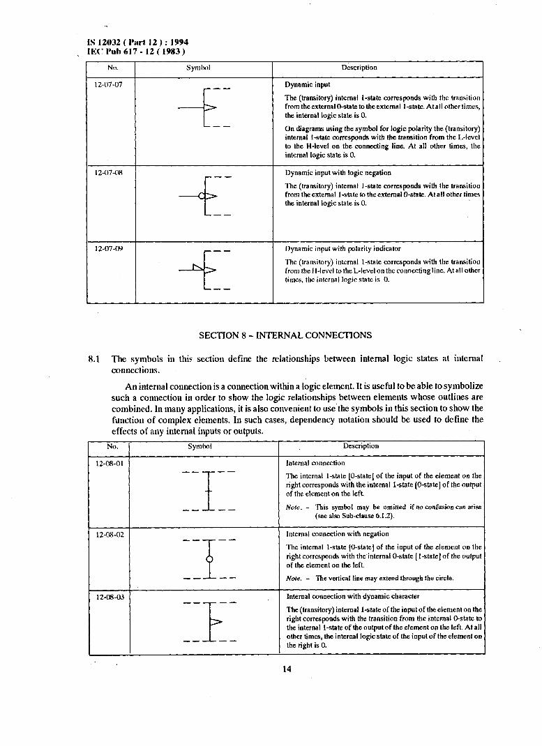
SECTION 8 - INTERNAL CONNECTIONS
8.1 The symbols in thk section define the relationships between internal logic states at internal coimections.
An internal comiection is a colmection within a logic element. It is useful to be able to symbolize such a connection in order to show the logic relationships between elements whose outlines are combined. In many applications, it is also convenient to use’the symbols in this section to show the function of complex elements. In such cases, dependency notation should be used to define the effects of any internal inputs or outputs.
No.
12-08-01
Symbol
-- --
I -- --
Description
Internal connection
The internal l-state [O-state] of the input of the element on the
right corresponds with the internal l-state [O-state] of tbe output
of the element on the left.
Note. - This symbol may be omitted if no confusion can arise
(see also Sub-clause 6.1.2).
12-08-02
12-08-03
-- --
1
internal connection with negation
The internal l-state [O-state] of the input of the element on the
right corresponb with the internal O-state [l-state] of the output
of the element on the left.
No&. - l%e vertical line may extend through the circle.
lntemal connection with dynamic character
The (transitory) internal l-state of the input of the element on the
right corresponds with the transition from the internal O-state tc
the internal l-state of the output of the element on the left. At all
other times, the internal logic state of the input of the element on
the right is 0.
14

IS 12032 f Port 12 ) : 1994 IEC I’uh 617 - 12 (iYX3 )
No. Symbol Descriplion
1 z-WM4 -- --
5 _- --
Internal cx~nnertion with negation and dynamic rhilrarlcr
The (transitory) internal I -slate ofthc input of lhc clcmc~lt OII IIIC
right correspond3 wilh the lransilion from the internal I- SIBIS lo
the internal 0-state of the oulpul of the element 011 tk Icti. Al all other times, the internal logic state of the input of the element on
the right is 0.
12-08-05 Internal input (virtual input)
-. .____ . . __This input always stands at its internal l-state unless it is affected
f
-G hy a dependency relationship that has an overriding or modifying
effect (see symbols 12-42-12 and 12-49-02).
--
Nob I. - internal inputs andoutputs have internal logicstates
only.
2. - Symh>ls of Section 7 shall not he applied lo internal
inputs and outputs, except symbol 12-07-07.
12-cB-06 --
1
Internal output (virtual output)
The effect of this output on an internal input lo which it is
connected must he indicated by dependmcy notation.
-- The notes with symbol 12X%-05 apply.
SECTION 9 - SYMBOLS INSIDE THE OUTLINE 9.1 If two or more iuputs have the same qualifying symbol for the function, they are assumed lo slalld
ii1 au OR-relation, except in the cases of hi-threshold aud exteusiou iuputs (see symbols 19-09-03 and 12-09-09) where the relatiouship should be appropriately indicated.
9.2 The descriptious of symbols 13-09-13 to 12-09-22 may give the reader the wroug impression that these are dyuamic iupuls. This is uot the case, as it must be remembered that the iuterual logic state as determiued by the exterual logic state or level may possibly be modified by the effect of othc: iuputs (e.g. Cm- inputs). If iuputs represeuted by symbols 13-09-l 3 to 1 Z-09-22 have a dynamic character, symbol 12-07-07 should be used in addition. See for example symbol 1 Z-47-01.
No. Symbol
12-09-01
-- 1
1
-- k
Postponed output
The change of the internal state of this output is postponed until
the input signal which initiates the change returns to it3 initial
external logic state or logic level. The internal logic state of any
input(s) affecting or affected by the initiating input must not
change while this initiating input stands at its internal l-state or
the resulting output state will not k bpecified by the symbol. If
the.input signal which initiates the change appears at an internal
connection, the change of state is postponed until the output of
the preceding element returns to its initial internal logic state.
No& 1. -
2. -
3. -
If this symhol is shown without prefix, it should IX
assumed that the output is postponed with respect to
eocll 4, +, +, -. T-input and to enclr Cm-input, OI
Cm+utput(seesymbols 12-18-01 and 12-18-02); inall
olher cases, the identifying numbers (or if necessary the
full lahels) of all inputs and outpub with respect to
which the output is postponed must ht: shown as a prefix
to this symbol. See symbol 12-19-15.
Care should be taken that this symbol is a right
angle with lines of equal length to avoid confusion
with other symbols, for example the character 7.
For the application of this symbol and additional
explanation, see Section 41.

IS 12032 ( h-t 12) : IYY-4 1K':<'1111~617 - l2( IY83)
If there arc IIO other iuputs with au overriding CIICCI, the trausitiou at the pulpit Iilkes l>lilCe whcu
t hC inpul ChilllgCS
- iu il di;lgrillll using lhr sylnhol for logic ucplion:
--EII3-
- in il diilgrillll using IhC Sylllbol for logiquc poliIrily:
from its external 1 -stale to its external O-state
from its external O-state to its cxterual 1 -Stilk
from its H-level to its L-level
from its L-level to its H-level
16

IS 12032 ( Part 12 ) : 1994 IEC Pub 617 - 12 (1983)
No Symbol Description
12-09-02
---II
--
_u-
--
Bi-threshold input
Input with hysteresis
The input takes on its internal l-state when the external signal level reaches a threshold value VI. It maintains this state until the external signal level has returned through Vl and reaches another threshold value V2. If this symbol (without the negation symbol or polarity symbol) appears on a diagram that uses either the symbol for logic polarity or the positive-logic convention, VI is more positive than V2. If it appears on a diagram that uses the negative-logic convention, Vl is more negative than V2. If the
negation or polarity symbol is present at the input. then the relationship between VI and V2 is reversed.
Norr. - If the label at the input line includesotl~ersymhols, symbol 12-09-02 shall be drawn adjacent IO the input line.
12-09-03 --
l-
0
--
Open-circuit output (e.g. open-collector, open-emitter. open- drain, open-source)
One of the two possible internal logic states of this type of output corresponds with an external high-impedance condition. In order lo produce a properlogiclevel in this condition, anextemally connected component or circuit, often a resistor, is required. This type of output is usually capable of forming part of a distrihuted connection.
Notes 1. - This symbol shall be drawn adjacent to the output line, except when using the bit-grouping symbol (symbol 12-09-25) in the manner defined in Section
25, where an alternative position is permitted.
2. - Although this symbol is shown inside the outline, it refers to external states and levels only.
3. - If it is necessary to indicate which logic level is the one with the low impedance, use can IX: made ot
symbol 12-09-04 or 12-09-05.
12-09-04 --
tr
l- --
(rpen-circuit output @I-type), for example PNPopen-mllector, NPK open-emitter, P-channel “opendrain”, N-channel “open-source”.
When not in its external high-impedance condition. this type 01 output products a relatively low-impedance It-level. See alxc
symbol 12-27-13.
Notes 1 and 2 with symhol 12-09-03 apply.
Nofe. - The meaning of this symbol is not altered hy the presence of a negation or polarity indicator.
12.~09-05 --
l-
4
--
Open-circuit output (L-type), for example NPN open-collector, PNP open-emitter, N-channel ‘*open-drain”. P-channel “open-
source”.
When not in its external high-impedance condition this type of output produces a relatively low-impedance L-level. See also symbol 12-27-13.
Notes 1 and 2 with symbol 12-09-03 and the note with symbol
12- 09-04 apply.
12-09-06 --
B
l- --
Passive-pull-down output
This type of output is similar to H-type open-circuit otltpu
(symbol 12-09-04) and can likewise be used as part of i distributed connectr<.n but without the need for an additiona external component or circuit. See also symbol 12-27-13.
Note 1 with symbol 12-09X)3 and the note with symbol t2-09-Of
a ppt y-
17

- IS 12032 ( Part 12 ) : 1994 IEC Pub 617 - 12 ( 1983 )
No.
12-09-07
12-09-08
12-09-09
12-09-10
12-09-11
Symbol
--
l-
V
-- -I
--i
--
E
--
--
l- E -- ---l
-- EN
L--
Description
Passive-pull-up output
This type of output is similar to the H type open circuit outpu
(symlml 12-09-05) and can likewise be used as part of : distributed connection but without the need for an additiona
external component or circuit. See also symbol 12-27-13.
Note 1 with symbol 12-09-03 and the note with symbol 12-09-0~
apply
3-state output
This output can take on a third external state, which is z high-impedance condition, having no logic significance.
For an example of use, see symbol 12-29-04.
Note 1 with symbol 12-09-03 applies.
Extension input
An input of a binary element to which the output of an extender
element may be connected (see symbol 12-09-10).
No/e. - The description which characlerizes the relationship
between the external logic states of binary variables ant
their corresponding physical quantities is normally no1
valid for exrension inputs and extender outpu&.
Extender output
An output of a binary element which may be connected to the
extension input of another binary element in order to extend the
number of inputs of that element.
The note with symbol 12-09-09 applies.
Enable input
If this input stands at its internal l-state, all outputs stand at their
normally defined internal logic states and have their normally
defined effect on elements or distributed connections that may
be connected to the outputs, provided no other inputs or outputs
have an overriding and contradicting effect.
If the input stands at its internal O-state, all outputs of the type
12-09-03, 12-09-04 or 12-09-05 are in their external high-im-
pedance condition?, all passive-pulldown outputs stand at their
high-impedance L-levels, all passive-pull-up outputs stand at
their high-impedance H-levels, all 3-state outputs stand at their
normally defined internal logic states and are in their external
high-impedance conditions and all other outputs stand at their
internal O-states.
Norr. - This input only affectsoutputs shown as external outputs.
If it is an input of an element having an internal connee-
tion indicated by oneof thesymbols 12-08-01 to 12-08-W
even-when the note IO symbol 12-08-01 is applied, the
input is also an EN-input of the element to which the
internal connection is connected. If ambiguity can arise,
forexamplein thecaseof embeddedoutlines, EN-depend-
ency as defined in Section 20 should be used.
,
18

IS 12032 ( Part 12) : 1994 IEC Pub 617 - 12 ( 1983)
f
l * -Ft EN
NO.
12-09-12
12-09-U
12-09-14
12-09-15
EN
EN*
1 t
.ENl l- I I
473-- * R *
Symbol
---I --
D
--
--i
-_
J
--
---L --
K
--
i
--
R
--
* EN1
= -Iii3 * ‘1
* 1
Description
D-input
The internal logic state of D-input is stored by the element. See
symbol 12-42-02.
N&T. - The internal logic state of this input is always subject to
an affecting input or output.
J-input
When this input takes on its internal l-state, al is stored by the
element.
When the input stands at its internal O-state, it has no effect on
the element.
K-input
When this input takes on its internal l-state, a 0 is stored by the
element.
When the input stands at its internal O-state, it has no effect on
the element.
Each occurrence of the combination J = K = 1 causes a single
change of the internal state of the output to its complement.
Clause 9.2 applies.
R-input
When this input takes on its internal l-state, a 0 is stored by the
element.
When the input stands at its internal O-state, it has no effect 011
the element.
19

IS 12032 ( Part 12 ) : 1994 IEC Pub 617 - 12 ( 1983 )
No. Symbol Description
12-09-16 S-input
When thisinput takeaon its internal l-state,a 1 isstored hythe element.
--II
-- When the input stands at ita internal O-state, it has no effect on
s the element.
The effect of the combination R = S = 1 is not specified by the
-- symbol; this effect may be indicated by means of SET/RESET-
dependency (see Section 19).
Clause 9.2 applies.
12-09-17
---II
-- T-input
Each time this input takes on its internal l-state, a single change T of the internal state of the output to its complement takes place.
When the input stands at, its internal O-state, it has no effect on -- the element.
Clause 9.2 applies.
12-09-1s Shifting input, left to right or top to bottom
Each time this input takes on its internal l-state, the information
---L
-- contained in the element will be shifted once m positions from
left to right or from top to bottom, depending on the orientation -em of the symbol for the element.
When the input stands at its internal O-state, it has no effect on -- the element.
Clause 9.2 applies.
No/r. - m shall be replaced by the relevent value. If m = 1, the 1
may be omitted.
12-09-1~ Shifting input, right to left or bottom to top
Each time this input takes on its internal I-state, the information
---I
-- contained in the element will be shifted once m positions from
right to left or from bottom to top, depending on the orientation cm
of the symbol for the element.
When the input stands at its internal O-state, it has no effect on -- the element.
Clause 9.2 applies.
The note with symbol 12-09-18 applies.
12-09-20 Counting up input
---II
-- Each time this input takes on its internal l-state, the count of
the element is increased once by m units.
+m When the input stands at its internal O-state, it has no effect on
the element. --
Clause 9.2 applies.
The note with symbol 12-09-18 applies.
12-09-21 Counting-down input
Each time this input takes on its internal l-state, the count of the
element is decreased once by m units.
When the input stands at its internal O-state, it has no effect on
the element.
Clause 9.2 applies.
The note with symbol 12-09-18 applies.
20

IS 12032 ( Part 12 ) : 1994 IEC Pub 617 - 12 ( 1983 )
No. Symbol Description
12-09-22 Query input of an associative memory
i
-- Interrogate input of an associative memory
? If this input takes on its internal l-state, an interrogation of the
content of the element takes place. --
If the input stands at its internal O-state, it has no effect on the
element.
Clause 9.2 applies.
12-09-23 Compare output of an associative memory --
f
Match output of an associative memory.
! The internal l-state at this output indicates a match.
--
12-09-24
3 _
-- Bit grouping for multibit input, general symbol
ml Inputs grouped by this symbol produce a number that is the sum
of the individual weights of the inputs standing at their internal m2 l-states. ‘The individual inputs shall be shown in ascending or
* descending order by weight.
I I
This number can be regarded:
. mk - as a number on which a mathematical function is performed,
or --
as defining an identifying number in the sense of dependency
notation (according to Clause 24.2) or
- as a value to become the content of the element.
mr . . . . nrtr shall be replaced by the decimal equivalents of the
actual weight?. If all weights are powers of 2, ml . . . . . ma may be
replated by the exponents of the powers of 2. fables between
ml and ma may be omitted to the extent that no confusion can
arise.
The asterisk must be replaced by an appropriate indication of the
operand on which the mathematical function is performed (e.g.
P or Q), by an appropriate indication in the sense of dependency
notation or by CT. Ir. the latter case, the number produced by the
inputs is the value that is loaded into the element.
12-09-25 Bit grouping for multibit output, general symbol
_
Outputs grouped by this symbol represent a number that is the
sum of the individual weights of the outputs standing at their
internal l-states. The individual outputs shall be shown in
ascending or descending order by weight.
This number can be regarded:
- as the result of the performance of a m‘athematical function, or
as the value of the content of the element.
mr . mk shall be replaced by the decimal equivalents of the
a&ral weights. If all weights are powers of 2, mt . . . . . mk may bt
replaced by the exponents of the powers of 2. labels betweer
mt and ma may be omitted to the extent that no confusion cnn arise.
The asterisk must be replaced by an appropriate indication of tht
result of the performance of the mathematical function or by CT.
In the latter case, the number represented by the outputs standing
at their internal l-states is the actual value of the content of tht
element.
21

IS 12032 ( Part 12 ) : 1994 IEC Pub 617 - 12 ( 1983 )
Illustrations
*
*
See also examples in Section 39
NO.
12-09-26
Symbol
i
--
Pm
--
Description
Operand input (Pm-input shown)
This inputrepresentsone hitofan operandon which oneor more
mathematical functions are performed.
Notes 1. - m shall be replaced by the dekimal equivalent 01
the weight of the hit. If the weights of all Pm-inputs
of the element are powers of 2, at each Pm-input m
may be replaced by the exponent of the power of
2.
2. - If an operand consists of two Or more bits repre-
sented by adjacent input lines, the bit grouping
symbol (12-09-24) may he used.
3. - Preferred letters for operands are P and Q. If these
letters are not suitable or if more than two operands
are involved, other characters may be used
providing no confusion can arise.
12-09-27 Greater-than input of a magnitude comparator
Nota l.- ‘Ihis symbol is intended for use when representing
cascaded comparators. For an example of use, see
symbol 12-39- 08.
2. - Symbols 12-09-27, I2-09-28 and 12-09-29 may be
combined to qualify inputs as follows: 2. CC, 3.
3. - This symbol should not he drawn ad.jacent to the
outline, to avoid cunfusion with the dynamic input
indicator symhol (12-07-07).
22

IS 12032 ( Part 12 ) : 1994 IEC Pub 617 - 12 ( 1983)
No.
12-09-28
Symbol
--iI
--
<
-I
Description
-
Less-than input of a magnitude comparator
Notes 1 and 2 with symbol 12-09-27 apply.
12-09-29 Equal input of a magnitude comparator
---II
-- Notes 1 and 2 with symbol 12-09-27 apply.
=
--
12-09-30
--
l-
*>* -
--
Greater-than output of a magnitude comparator
NOILCT 1. - The asterisks shall be replaced by designations 01
the operands, for example P and 0 respectively.
2. - Symhnls 12-OY-30, 12-09-31 and 124Y-32 may Ix
combined to qualify outputs as fullowx
*r*,*s*,>,.
2. - If this symbol appears in one element of a series ol
cascaded comparators, the output marked with thi:
symbol is affected not only hy the operands, hut alsc
by the inputs marked with the symbols 12-W-27
1 Z-09-28 or 12-09-29.
12-09-3 1 --
Less-than output of a magnitude comparator
-- I-
The notes with symbol 12-09-30 apply.
*<*
12-09-32 --
I-
Equal output of a magnitude comparator
The notes with symbol 12-09-30 apply.
*=* No/r. - If this synrh>l is no1 combined with symlx>l IL-W-XI 11
symbol 12-09-31, the designationsof the operands may h --
omitted providing no confusion can arise.
12-09-33
--I
--
61
--
Rorrow-in input of an arithmetic element
No/r. - A nurnl~er may be added as a suffix IO this label: thi:
number is the exponent of the power of ?. which is th
weigh of the hit involved.
12-09-34
iI
--
BG
--
Borrow-generate input of an arilhmelic elcmcnt
The note with symbol 12-W-33 applies.
12-09-35 --
BG
-- l-
The note with symbol 12-W-33 applies.
liorrow-generatc output of an arithmetic clcmcnt
23
IS 12032 ( Part 12 ) : 1994 IEC Pub 617 - 12 (1983)
No. Symbol Description
120-36 --
l-
fbrrow+xH output of an arithmetic element
Ripple-borrow output of an arithmetic element BO
The note with symbol 12-09-33 applies.
--
t 2-(w-37 Borrow-propagate input of an arithmetic element
---F
--
The note with symbol 12-00-33 applies.
BP
--
12-OY-3X Borrow-propagate output of an ariihmetir element --
l-
The note with symbol 12-W-33 applicx.
BP
--
12-0%3Y Carry-in input of an arithmetic element
-II
-- The note with symbol 12-W-33 applies.
Cl
--
12-0%40
--iI
-- Carry-gencrale inpul of an +rithmetic elsment
CG The nok with symbol 12-OY-33 applies.
--
12-09-41 C’arry-pcncratc output of an arithmetic element --
l-
The note with symbol 12-W-33 applies.
CG
--
12-OY-42 Carry-oul output of an arithmetic element --
I--
Ripple-carry output of an arithmclir elcmcnt
co ‘l‘hc note with symhd 12-(W-33 applicx.
--
12-W-43 Carry-propagate input of an a
---II
-- ‘l‘hc nok will1 symbol 12-W43 applic\.
CP
--
12-(R-44 --
I-
(‘;lr-ry-llr[‘I’;lF;lt” output tll. ~111 ~Irithm~lic. cl<.nk’nt
‘1‘11~~ note with hynlh~d I .2-(W-23 ;Ipplil,\
CP
--

IS 12032 .( Part 12 ) : 1994 IEC Pub‘617 - 12 ( 1983 )
I No. Symbol Description
12-05-45 Content input
--I
-- m shall be replaced by an appropriate indication of the conter
of the element (e.g. a counter) that results whenever this inpu
CT=m takes on its internal l-state.
If this input stands at its internal O-state, it has no effect on th -- element.
For an example of use, see symbol 12-49-16.
12-09-46
--
‘&J*
l- --
Content output
The asterisk shall be replaced dy an appropriate indication o
those values of the content of the element (e.g. a counter) fo
which the output stands at its internal l-state.
For an example of use, see symbol 12-49-12.
12-09-47 Line grouping at the input side
2
-- This symbol indicates that hvo or more connections are needel
to implement a single logic input.
I For an example of use, see symbol 12-28-06.
I Norr.s. 1. - The logic levels on connections grouped hy thi
- symbol may differ from those on the other input an
output pins. --
2. - For an example of use of Note 1, see symbu
12-29-07.
12-09-M Line grouping at the output side
--
L
~iis symbol indicates that two or more connections are needel
lo implement a single logic output.
I
For an example of use, see symbol 12-2x-07.
I Note 1 with symbol 12-09-47 applies.
--
12-09-49 Fixed-mode input
If an element can perform several funcfions but only a restrictes
_[
-- number of functions is of interest, this representation can I*: uw IO identify an input that must he in the internal l-state for 111
I, I, 1 element to perform the functions of inlertM indicated by lli symbol.
-- A fixed mode input must not be affected by dependency notalio
nor have other functions.
For examples of WC, see symbols 12-49-07 and 12-4WJX.
12-W-50 --
l-
I, ,I 1
--
I:ixcJ stale output
This reprc~enlalion may hc used to identify an output lhat elway stands at its internal I-stale.
A fixed-slatcoulput must not I~caffccld by dcpdcncy nolalio
nor have olkr funclious.
Ibr RI, example of use. WC symbol 12-33-10.
25

IS 12032 ( Part 12 ) : 1994 IEC Pub ii17 - 12 (1983 )
SECTION 10 - NON-LOGIC CONNECTIONS AND SIGNAL-FLOW INDICATORS
10.1 Symbol 13-02-01 or 13-02-02 of IEC Publication 617-13 may be used to denote an input or an output carrying analogue or digital signals respectively.
10.2 For supply voltage inputs having special effects, use symbol 13-03-l 1 of IEC Publication 617-13.
10.3 In principle, the direction of signal flow is from left to right and from top to bottom. If this rule camlot be maintained or the direction of signal flow is not obvious, then the signal lines should be marked with arrowheads pointing in the direction of signal flow. These arrowheads shall not touch the outline or any qualifying symbol. See for example, symbol 12-29-03.
No.
12-10-01
Symbol
-c
--
--
Description
Non-lcgic connection, shown on the left-hand side
This symbol may be used to indicate a connection which does
not carry any logic information (e.g. reference voltage
connection).
Norr. - Additional information associated with non-logic connec- tions may be shown without brackets inside the outline.
For an example of use, see symbol 12-47-02.
12-10-02 Use symbol 02-05-03 Ridirectional signal flow
For an example of use, see symbol 12-29-08.
Notes. 1. - On a connecting line with bidirectional signal flow,
any symbol for logic polarity should point to the
right or down e.g.:
-+L
-- --
and
-- -- l+
2. - In some cases, the appearance of the symbols for
logic polarity makes the use of the symbol of
bidirectional signal flow unnecessary, e.g.:
26

IS 12032 ( Part 12 ) : 1994 WC Pub 617-12 ( 1983 )
CHAPTER IV : DEPENDENCY NOTATION
SECTION 11 - GENERAL EXPLANATlON
Dependency notation is a means of denoting the relationships between inputs, outputs, or inputs and outputs, without actually showing all the elements and interconnections involved.
Apart from its use in complex elements, dependency notation should not be used to replace the symbols for combinative elements.
The information provided by dependency notation supplements that provided by the qualifying symbols for an element’s function.
In the convention for dependency notation, use will be made of the terms “affecting” and “affected”. In the case where it is not evident which inputs must be considered as being the affecting or the affected ones (e.g. if they stand in an AND relationship), the choice may be made in any convenient way.
In some complex elements, outputs may have an effect on inputs and other outputs. For the sake of simplicity, thefext of Sections 12 and 13 refers to “affecting inputs” only, but it should be understood that the recomm&ded notation applies to affecting outputs also.
SECTION 12 - CONVENTION
Dependency notation usually defines relationships between internal logic states. However, in the case of 3-stale outputs, passive-pull-down outputs, passive-pull-up outputs, and open-circuit outputs (symbdls 12-09-03 through 12-O9-OS), ENABLE dependency (section 20) defines relationships between the internal logic states of affecting inputs and the external states of affected outputs.
Application of dependency notation is accomplished by:
- labelling the input affecting other inputs or outputs with a particular letter symbol denoting the relationship involved followed by an identifying number;
- labelling each input or output affected by that affecting input with that same number.
If it is the complement of the internal logic state of the affecting input [output] that does the affecting, a bar shall be placed over the indentifying number at the affected input [output]. For an example of use, see symbol 12-42- 11.
If the affected input or output requires a label to denote an effect it has on the clement, this label shall be prefixed by the identifying number of the affecting input.
If an input or output is affected by more than one affecting input the identifying numbers of each of the affecting inputs shall appear in label of the affected one, separated by commas. The left-to-right order of these identifying numbers is the same as the sequence of the affecting relationships (see also Section 25).
Wo affecting inputs labelled with different letters shall not have the same identifying number unless one of the letters is A (see Section 23).
If two affecting inputs have the same letter and the same identifying number they stand in an OR relationship to each other.
If the labels denoting the functions of affected inputs or outputs must be numbers (e.g. outputs of a coder), the identyfying numbers to be associated with both affecting inputs and affected inputs or outputs shall be replaced by another character selected to avoid ambiguity, for example Greek letters.
An affecting input affects only the corresponding affected inputs and outputs of the symbol.
SECTION 13 - TYPES OF DEPENDENCY
13.1 The following types of dependency are defined:
AND, OR and NEGATE dependencies are used to denote Boolean relationships between inputs and/or outputs.
27
IS12032(Part12):1 4 7 IEC Pub 617-12 ( 1983
INTERCONNECTION, dependency is used to indicate that an input or output imposes it logic state on one or more other inputs and/or outputs.
CONTROLdependency is used to identify a timing input or a clock input of a sequential element and to indicate which inputs are controlled by it.
SET and RESET dependencies are used to specify the internal logic states of an RS-bistable element when the R-and S-inputs both stand at their internal l-states.
ENABLE dependency is used to identify an Enable input and to indicate which inputs and/or outputs are controlled by it (e.g. which outputs take on their high-impedance condition).
MODE dependency is used to identify an input which selects the mode of operation of an element and to indicate the inputs and/or outputs depending on that mode.
ADDRESS dependency is used to identify the Address inputs of ti memory.
Table 1 page 51, lists the various dependencies and summarizes their effects. More detailed definitions appear in the following sections, together with illustrations df the concepts. In these illustrations, general symbols explained in Chapter V are used.
In Table 1, the word “action” implies:
- that affecting inputs will have their normally defined effect on the function of the element;
- that affected outputs will take on the intemal logic states detenneined by the function of the element.
,
TABLE I Types of dependency
-
I T Effect on affected input or output if the affecting input stands at its: See Section
Letter(s) rype of dependency O-state
Prevents action (address not selected)
Prevents action
23
18
- Prevents action of affected inputs
- Imposes external high-impedance
condition on open-circuit and 3-state
outputs (internal state of 3-state out-
puts unaffected)
20
- imposes high-impedance L-level on
passive-pull-down outputs and high-
impedance H-level on passive-pull-up
outputs
- Imposes O-state on other outputs
Imposes O-state 4 ’
Prevents action (mode not selected)
No effect
No effect
14
21
16
19
No effect 19
Permits action
Imposes O-state
15
17
‘over it is affected by the logic state of th affecting inpu
1 -state
Permits action (address selected)
Permits action
Permits action
A ADDRESS
CONTROL
ENABLE
c
EN
Permits action G AND
MODE M Permits action (mode selected)
I NEGATE N Complements state I
RESET R Affected output reacts as it would
dotoS=O,R=l.
I SET S I Affected output reacts as it would
dotoS=l,R=O
I
I OR
j :~~l!ECllON
Note. - An affecl input [output] carrying an identifying number with a I which is the complement of 1ha1 indicated in the table above.
IS 12032 ( Part 12 ) : 1994 IEC Pub 617-12 ( 1983 )
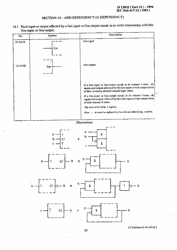
SECTION 14 - AND DEPENDENCY (G-DEPENDENCY)
14.1 Each input or output affected by a Gm-input or Gm-output stands in an AND relationship with this Gm-input or Gm-output.
No. Symbol
12-14-01
12-14-02
~ ~
-c C-
Gm
--
--
Gm
-- ,I---
_. Illustrations
a
b
C
a
b I
Description
Gm-input
If a Gm-input or Gm-output stands at its internal l-slate, all
inputs and outputs affected by this Gm-input or Gm-output stanc
at their normally defined internal logic states.
If a Gm-input or Gm-output stands at its internal O-state, al
inputs and outputs affected by this Gm-input or Gm-output stant
at their internal O-states.
The note with Table I applies.
Note. - m must be replaced by the relevant identifying number.
b

IS 12032 ( Part 12 ) : 1994 IEC Pub 617-12 ( 1983 )
----
1 ---- I ----
a
b
1
G2
-i
----
= 1
G3
3 1 ----- 1
GG I i ---- a
b
SECTION 15 - OR DEPENDENCY (V-DEPENDENCY)

IS 12032 ( Part 12 ) : 1994 IEC Pub 617-12 ( 1983 )
b
= - b
SECTION 16 - NEGATE DEPENDENCY (N-DEPENDENCY)
16.1 Each iuput or output affected by au Nm-input or Nm-output stands in au EXCLUSIVE-OR rclatiouship with this Nm-input or Nm-output.
No.
12-16-01
12-16-02
Symbol
---L
--
Nm
Nm-input
--
-- Nm-output
Nm
IkWriptinn
.
-- l-
If an Nm-input or Nm-output stanb at its internal I-slale. th internal logic state of each inpul and each output affected by thi! Nm-input or Nm-output is the complement of the normall! defined internal logic state of thal input or output.
If a11 Nm-input or Nm-output shnds at its inlernal O-stoic, al inputs and outputs affected hy this Nm-input or Nm-output stanc at their normally Mined internal logic states.
The notes with Table I and symbols 12-14-01 ;IIIJ 12-14-O;
HPPlY.
Illustmtiort ----
b i -
b
=1 Ifi1 = 0, Ihlw (‘ = I?
CEO.----- II’;1 = I, llllw (‘ = I,
-C
31 "

IS 12032 ( Part 12 ) : 1994 IEC Pub b17-12 ( i983 )
SECTION 17 - INTERCONNECTION DEPENDENCY (Z-DEPENDENCY)
17.1 INTERCONNECTION dependency is used to indicate that an input or output imposes its internal logic state on one or more other inputs and/or outputs, for an example of use, see symbol 12-28-13.
The internal logic state of an input or output affected by a Zm-input or Zm-output is identical to the internal logic state of its affecting Zm-input or Zm-output unless modified by additional dependency notation.
No. Symbol Description
12-17-01
-c
-- Zm-input
Zm
--
12-17-02 -- Zm-output
Zm
-- l- If a Zm-input or Zm-outputstands at its internal l-state, all inputs
and outputs affected by this Zin-input or Zm-outputstand at their
internal l-states unless modified by additional dependency nota-
tion.
If a Zm-input or Zm-output stands at its internal O-state, all input3
andoutputs affected by this Zm-ioputorZm-outputstandattheir
internal O-states unless modified by additional dependency
notation.
The notes with Table I and symbols 12-14-01 and 12-14-02
apply.
a
Illustrations --- r 7 b
----_- v
- 1 3-a = 4
d-----d .
-1
32

IS 12032 ( Part 12 ) : 1994 IEC Pub 617-12 ( 1983 )
a
b
a = - b r C SECTION 18 - CONTROL DEPENDENCY (C-DEPENDENCY)
18.1 CONTROL dependency shall be used for sequential elements only and may imply more than a simple AND relationship. It identifies an input that produces action, for example the clock of an edge-triggered bistable circuit or the data enable of a 1eveLoperatCd transparent latch.
No. SymM Description
12-18-01
-I
-- Cm-input
Cm
--
12-18-02
--
Cm
-- l-
Cm-output
If a Cm-input or Cm-output stands at it5 internal l-state, the
inputs affected by this Cm-input or Cm-output have their
normally defined effect on the function of the element.
If a Cm-input or Cm-output stands at its internal O-state, the
inputs affected by this Cm-input or Cm-output have no effect on
the function of the element.
The notes with Table I and symbols 12-14-01 and 12-14-02
apply. \
Illustrations
4--
G
b
C
cl- G & &
b- 8 8
b 4-J Cl 3

IS 12032 ( Part 12) : 1994 IEC Pub 617-12 ( 1983 )
Use has been made of Clause 9.1
a
b
C
r--- a Gl
E b lC2 This illustntion has been included for explanatory purposes, but the use of a Cm-input to affect a secoud Cm-input is not recommended.
For comparison of C-, EN- and M-effects ou inputs, see Sectiou 22.
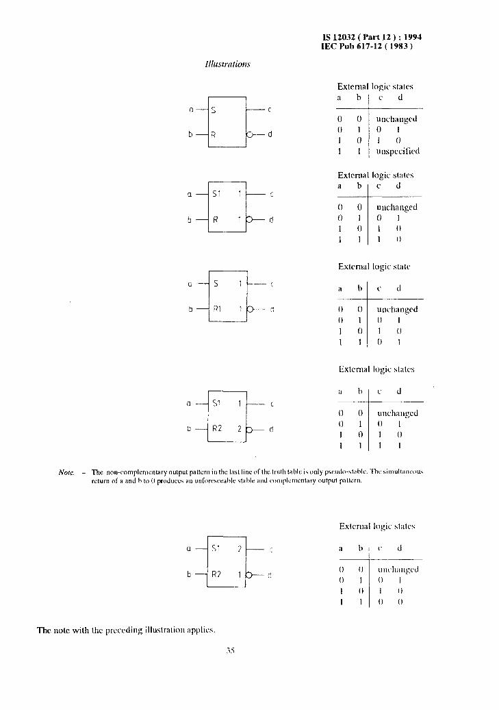
SECTION 19 - SET AND RESET DEPENDENCY (S- AtiD R-DEPENDENCY)
19.1 SET aud RESET dependencies are used if it is necessary to specify the effect of the combination R = S = 1 ou a histable element. These dependencies should uot be used if such specification is uot necessary.
Affecting S- aud R-inputs can affect outputs only.
No.
12-19-01
Symbol
---II
--
Sm
--
Description
Sm-input
If an Sm-input stands al its internal l-state, the outputs affected
by this Sm-inputwill take on the internal logic state they normal-
ly would take on for the combination S= 1. R=O, regardless of the
state of any R-input.
If an Sm-input stands at its internal O-state. it has no effect.
The notes with Table I and symbols 12-14-Oi and 12-14-02
“PPlY.
12-19-02
+-
--
Rm
--
Rm-input
Han Km-input stands at its internal l-state, the outputs affected
by this Rm-input will take on the internal logic state they nor-
mally would take on for the combination S=O, R=l, regardless
of the state of any S-input.
If an Rm-inpuistands at its internal O-state, it has no effect.
The notes with Tahle I and symbols 12-14-01 and 12-14-02
“PP’Y.
34
IS 12032 ( Part 12 ) : 1994 IEC Pub 617-12 ( 1983 )
Illustratioris
b d
b--/RI +--II
I 1
Extenlal logic states a b c d
0 0 unch;lnged
I----
0 1 0 1 1 0 I 0 1 1 uuspccified
External logic states a b c d
0 0 uuchaugcd
-I---
0 1 0 1 1 0 1 0 1 1 1 0
Extend logic stilte
a blc d
0 0 I lIIICtlilIl~Cd
0 1 0 I
1 0 1 0 1 1 0 1
Extcnlill logic stiitcs
Note. - The non-complementary output pattern in the last line of the truth tahlc isonly pseudo-st;~hlc. ‘lhc simultaneous
return of a and h to 0 products an unforesxahle stable and complementary output pattern.
Extcn~l logic states
a h , (’ cl
-I 0 0 0 1 Ull(.llillI~:('Ll 0 i
1 0 I 0
I I 0 0
The uotc with the prcccdiug illustr;ltiou ;Ipplies.
IS 12032 ( Part 12 ) : 1994 IEC Pub 617-12 (1983)
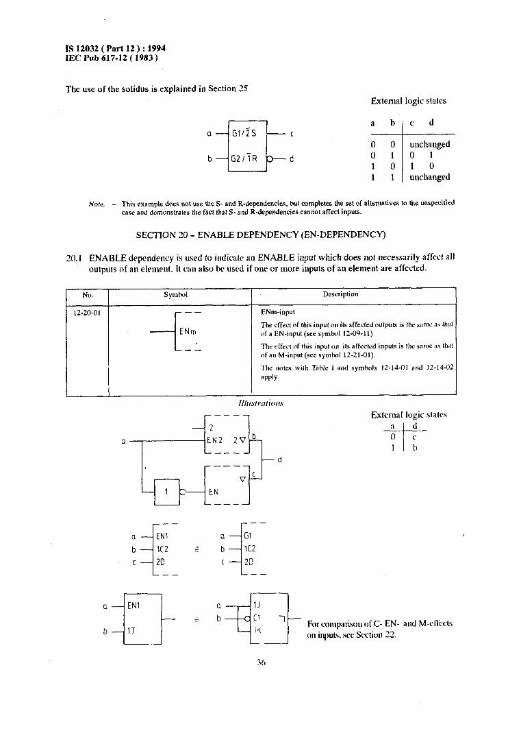
The use of the solidus is explained in Section 25
External logic states
Note. - This exAmpIe does not use the S- and R-dependencies, hut completes the set of alternatives to the unspecified
case and demonstrates the fact that S- and R-dependencies cannot affect inputs.
SECTION 20 - ENABLE DEPENDENCY (EN-DEPENDENCY)
30.1 ENABLE depeudeucy is used to indicate an ENABLE input which does not necessarily affect all outputs of an element. It can also be used if oue or more inputs of an element are affected.
NO.
12-20-01
Symbol
--
--I
ENm
--
Description
ENm-input
The effect of this input on its affected outputs is thr same as that
of a EN-input (see symbol 12-09-11)
The effrct of this input on its affected inputs is the same as that
of an M-input (see symbol 12-21-01).
The notes with Table I and symbols 12-14-01 and 12-14-02
apply.
Illrr.stn7tion.s
d
External logic states a d
t 0 c 1 h

IS 12032 (Part 12 ) : 1994 IEC Pub 817-12 ( 1,983 )
SECTION 21 - MODE DEPENDENCY (M-DEPENDENCY)
31.1 MODE depcndcncy is used to indicate that the effects of particular inputs a11d outputs of an ~I~IW.WI depend on the mode in which the element is operating.
NO.
12-21-01
12-21-02
21.2
- Symbol
--I --
Mm
--
--
Mm
-- l-
I
-
Description
Mm-input
Mm-outpul
If an Mm-input or Mm-output stands at its internal I-state, the inputs affected hy his Mm-input or Mm-output hnve their nor- mally defined effect on the functhn of the element and the outputs affected hy this Mm-input or Mm-output stand at their normally defined internal logic states. i.c,. the inputs ad output< are cnalhl.
I.
‘l‘hc notes with table 1 and symlwl IZ- I441 and 12-14-02 apply.
111 COIII~ICX clemcnts with il large IIUI~C~ of different Illodes, ;Ippliciltiol~ of the convcntioo for MODE depcndellcy IWI~ lead to a very extcllded labelling. III such cilscs, the inputs illld oLltpuIs affected by any affcctillg M-input arc simply Ii~bellcd with the lcttrr M, hut thrn the di;lgr;llll cot~ti~it~illg Ihc sy111b01 IINN itISO contain cithcr i1 Iilhlc in which Ihc cffccls of lhcsc inpuls in lhc
different Inodcs arc clr;lrly cxplaincd or ii skltcmcnt ;Is IO whcrc sttch ;I tahlc is lo hc f0~11d. If 110 confusion c;lIl arise, ~hcsc lrttcrs M may he omitted.
The USC ol’ the bit-grouping symbol and the solidus is rxpl;lillrd irl Scctious 34 illld 3, rcspcclivcly.
M-dcpcndcncy affecting iq~uts:
$1 5 $1
77
,

IS 12032 ( Part 12 ) : 1994 IEC Pub 617-12 ( 1983 )
I I a
--t? c4/2-k/3+
I
d 2,4D
e 1,4D
f -+.4D t-
Determining the function of an output :
Mode 0 (b = 0, c = 0): the outputs remain at their existing states as none of the inputs has an effect.
Mode I (b = 1, c = 0 ): parallel loading takes palce through inputs
e and f.
Mode 2 (b = 0, c = 1) : shifting down and serial loading through input d take place.
Mode 3 (b = 1, c = 1) : counting up by increment of 1 per clock pulse takes palce (input a).
If input a stands at its internal l-state establishing mode 1, output b will stand at its internal 1 -state if the content of the register equals 15. If input a stands at its internal O-state, output b will stand
at its internal l-state if the content of the register equals 0. For explanation, see also Section 25.
I I
I
Modifying dependent relationships of outputs :
At output e the label set causing negation (if c = 1) is effective in modes 2 and 3 only. In modes 0 and I, this output stands at its normally defined state as if it had no labels.
At output f the label set has effect if the mode is not 0, so output f is negated (if c = 1) in modes 1, 2 and 3. In mode 0 the label set has no effect so the output stands at its normally defined state. In this example 0,4 is equivalent to (l/2/3) 4.
At output g there are two label sets. The first set, causing negation
(if c = l), is effective only in mode 2. The second set, subjecting g to AND dependency on d, has effect only i3 mode 3.
Note that in mode 0 none of the dependency relationships has any effect on the outputs, so e, f and g will all stand at the same sta’e.
For comparison of C-, EN- and M-effects on inputs, see Section 22.
SECTION 22 - COMPARISON OF C-, EN- AND M-EFFECTS ON INPUTS
1
With regard to affected input, Cm-, ENm- and Mm-inputs all have the satne effect. However, their intended applications are different:
- Cm should be used to identify an input that produces action;
- ENm should be used to identify an input that produces a single preparatory effect;
38

IS 12032 ( Part 12 ) : 1994 IEC Pub 617-12 ( 1983 )
- Mm should be used to identify one or more inputs that singly or together produce alternative preparatory effects.
SECTION 23 - ADDRESS DEPENDENCY (A-DEPENDENCY)
23.1 ADDRkSS dependency provides a clear representation of those elements, particularly memories which use address control inputs to select specified sections of a multidimensional array. ADDRESS dependency allows a symbolic representation of only a single general case of the sections of the array, rather than requiring a symbolic presentation of the entire array. An input of the array shown at a particular element of this general section is common to the corresponding elements of all sections of the array. An output of the array shown at a particular element of this general section is the result of the OR function of the outputs of the corresponding elements of the selected sections. If any other function than OR is performed, this should be indicated by adding the appropriate
qualifying symbol below the general qualifying symbol, e.g. RAM
a0
If the label of an output of the array shown at a particular element of this general section indicates that this output is an open-circuit output or a 3-state output, then this indication refers to the output of the array and not to those of the sections of the array.
Inputs which are not affected by any affecting ADDRESS input have their normally defined effect on all sections of the array whereas inputs affected by an ADDRESS input have their normally defined effect only on the section selected by the ADDRESS input.
An affecting ADDRESS input is labelled with the letter A followed by an identifying number which corresponds with the address of the particular section of the array selected by this input.
Within the general section presented by the symbol, inputs and outputs affected by an Am-input are labelled with the,letter A, which stands for the identifying numbers, i.e. the addresses of the particular sections1 This letter A is subject to the rules of dependency notation concerning identifying numbe& associated with affected inputs and outputs.
If an output affected by an Am-input also has other labels, then the labels preceding the letterA affect the output of the section selected by this Am-input and the labels placed behind the letter A affect the output of the array i.e. after the application of the OR function (or the indicated function) to the corresponding outputs of the selected sections of the array.
Illustration
a- EN1
a- Al b-EN2
b - A2 c-EN3
c -A3 d - C4
d-C4 1 r -.
1 r = e l.lrD 1 >,I
e - A,40 A-f - 2,4 D 2 -f
- 3,4D 3
9- -h 9 - 1.40 1 %l - 2,4D 2 -h
- 3,4D 3
39

IS 12032 ( Pi-t 12 ) : 1994 IEC Pub 61’7-12 ( 1983 )
23.2 The identifying numbers of affecting ADDRESS inputs correspond with the addresses of the sections selected,by these inputs. They need not necessarily differ from those of other affecting dependency-inputs (e.g. G, V, N, . ...) because in the general section presented by the symbol they are replaced by the letter A.
If there are several sets of affecting Am-inputs for the purpose of independent and possibly simultaneous access to sections of the array, then the letter A is modified to lA, 2A, . . . . . . Because they have access to the same sections of the array, these sets of Am-inputs may have the same identifying numbers.
Nero affecting ADDRESS inputs having the same identifying number stand in no relation to each other nor to any affecting dependency-input (e.g. Gm, Vm, Nm, . ..) having the same identifying number.
No.
12-23-01
sphi
--I
--
Am
--
Am-input
Description
If this input stands at its internal l-state, the inputs affected by
this input (i.e. the inputs of the section of the array selected by
this input) have their normally defined effect on the elements 01
the selected section and the internal logic states of the outpuu
affected by this input (i.e. the outputs of the selected section:
have their normal effect on the OR functions (or the indicatec
functions determining the internal logic states of the outputs 01
the array.
If the input stands at its internal O-state, the inputs affected b!
this input (i.e. the inputs of the section selected by this input:
have an effect on the elements of this section and the outpuu
affected by this input (i.e. the outputs of the section selected by
this input) have no effect on the outputs of the array.
The notes with Table I and symbols 12-14-01 and 12-14-02 apply
Illustration The use of the bit-grouping symbol is explained in Section 24.
0
I! 0 *TS
3
Cl J r Array of 16 sections, each of 4 pulse-
- A.10
1
1A - triggered D-bistables (see Section 41).
40

IS 12032 ( Part 12 ) : 1994 IEC Pub 617-12 (1983) ----
2A $-
2A$
suppose a = 1
A particular section (among 8) is selected if it is selected by both sets of Am-inputs.
A particular section (among 8) is selected if it is selected either by one or by both sets of Am-inputs.
The internal logic states of the OUI-
a puts of the array arc the results of the OR functions of the complcmcnls of
----- the logic states of the outputs of thr
3.A t-- selected sections.
L _------ -I-- 41
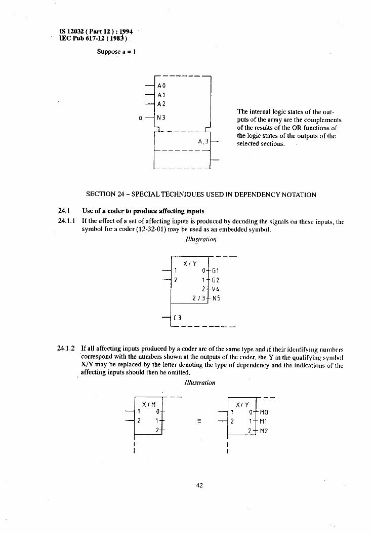
1!312032(Part12):194 lEC Pub 617-12 (198 d )
Suppose a = 1
A0
Al
The internal logic states of the out- a puts of the array are the complements
of the results of the OR functions of ----- the logic states of the outputs of the selected sections.
L ------ + SECTION 24 - SPECIAL TECHNIQUES USED IN DEPENDENCY NOTATION
24.1 Use of a coder to produce affecting inputs
24.1.1 If the effect of a set of affecting inputs is produced by decoding the signals on thcsr inputs, the symbol for a coder (12-32-01) may be used as an embedded symbol.
Illuptiort
24.1.2 If aI affecting inputs produced by a coder are of the same type and if their identifying numbers correspond with the numbers shown at the outputs of the coder, the Y in the qualifying symbol X/Y may be replaced by the letter denoting the type of dependency and the indications of the affecting inputs should then be omitted.
Illustration
42

IS 12032 ( Part 12 ) : 1994 IEC Pub 617-12 ( 1983 )
14 7 1 ._ Use of hit grouping to produce affecting inputs
34.2.1 If all affecting iuputs produced by a coder are of the same type and have consecutive identifying nunlberj (not necessarily corresponding with the numbers that would have been shown at the outputs of the coder), the bit grouping symbol (symbol 12-09-24) can be used. In this case, the asterisk shall be replaced by the letter denoting the type of dependency followed by 2. The ml shall be replaced by the smallest identifying number aud the m2 shall be replaced by the largest. The range of the identifying numbers (m2 - ml +l) must equal the number of outputs of the coder.
Illustrations
T --
0 0 - A7
2
-se
0
8G;
2 1 - I =
G8
I
i
---
X/Y ‘0 A0
1 Al
1 2 A2
2 3 A3
L 4 A4
5 A5
6 A6
? A3
i
G8
I
43

IS 12032 ( Part 12 ) : 1994 IEC Pub 617-12 (1983)
24.3 Designation of lahelled inputs having inherent storage
x3.1 It ofteu occm that a labelled input other than a D-input has inherent storage. Such au input may be iabciied as:
in which
mD,*
- m shall be replaced by the identifyiug numbers of the inputs that affect the storage operation;
- the asterisk shall be replaced by the symbol denotiug the fuuction of the stored input. If that symbol is a number, the comma following the D may be omitted.
a
b
a
b
r----
Illustrations
M2
a = - b
EN
r ---- a
b Sed also Sectiou 25.
SECTION 25 - THE ORDERING OF LABELS ASSOCIATED WITH INPUTS AND WITH OUTPUTS
25.1 Order of input labels
25.1 .l If au input cxcrtiug a siuglc fuuctiou is affcctcd, by other inputs thr qualifying .iyu~bol for that fuuctiou shall bc preceded by the labels corrcspouding to the affcctiug inputs. The left-to-right order of thcsc pccediug labels shall bc the order in which the rffccts or nlodificatious nlust bc appiicd. The affccIcd iuput I’X~T~P IX? fmcliou if the logic slate of any out of the al’fccliug inputs or outputs, colaidcrcd scparateiy , would cause I hc affccIcd input IO havr IIO rfl‘ct, rcgardicss of the logic St;llC% Of other iIlfCCtiIlg inputs.
44
IS 12032 ( Part 12 ) : 1994 IEC Pub 617-12 ( 1983 )
Illustration
----
a EN1
b
I
C2 If either a = 0 orb = 0, then c has no
C I,20 effect.
----
25.1.2 If an input exerts more than one function or has more than one set of labels of affecting inputs, the indications of these functions or these sets may be shown on different input lines, which must be connected together outside the outline (see examples 12-33-07, 12-49-11, 12-49-15). However, there are cases in which this method of presentation is not advantageous. In those cases, the input may be shown once with the different sets of labels separated by solidi. No meaning
is attached to the order of these sets of labels. If one of the functional effects of an input is that of an unlabelled input of the element, a solidus shall precede the first set of labels shown (see e.g. symbol 12-49-l 3).
Zllustratiom
--I --
a IGl --
a
b
--
a
b
C
= - a --T Cl --
a--m- =
- “-v Cl L--e
a -r;l--- - = b G2
iR
C 1,2R
2.5.1.3 If all inputs of a combinative element are disabled (caused to have no effect on the function on the element), the internal logicstates of the outputs of the element are not specified by the symbol.
If all inputs of a sequential element are disabled (caused to have no effect onthe function of the element), the content of this element is not changed and the outputs remain at their existing
internal logic states.
25.1.4 Labels may be factored using algebraic techniques.
Zllustratiom
-------
--I?
- --------
1,2,3,4[5+/ 6-I E ------- -IT
1,2,3,4,5+/1,2,3,4,6- ------- -
45

IS 12032 ( Part 12 ) : 1994 IEC Pub 617-12 ( 1983 )
25.1.5 If, at inputs without inherent storage, algebraic factoring techniques are combined with the use of the bit grouping symbol, labels common to all inputs may be shown behind the bit grouping symbol provided the proper order of all labels is maintained.
Illustrations
1! ---
G4 } = 4,1
42 Mf -
---
1’ ---
G4
1
2 I
4M$
L-__
= -
r----
----
25.1.6 If, at inputs having inherent storage, algebraic factoring techniques arc combined with the use of the bit grouping symbol, the indication “mD,“, as defined in Clause 24.3, may also bc placed behind the bit grouping symbol provided the proper order of all other labels is maintained.
Illustrfltioti
b
C
d
25.2 Order of output labels
25.2.1 If an output has a number of different labels, regzrtlless of whether they arc identifying numbers of affecting inputs or outputs or not, these labels shall be shown in the following order:
- if the postponed output symbol (12-09-01) has to be shown, this COIIKS first, if ncccss;lry preceded by the indications of the inputs to which it must be applied;
- followed by the qualifying symbols determining or modifying the internal logic state of the output, such that the left-to-right order of these labels correspond with the order in which their effects must be applied for application, see symbol 12-49- 15;
- followed by the label indicating the effect of the output 011 inputs and other outputs of the element.
Symbols for open-circuit, passive-pull-down, passive-pull-up, or 3-state outputs shall be drawn adjacent to the output line, except when using the bit grouping symbol as described in Sub-clause 25.2.3<
If an output needs several different sets of labels which can be considered to stand in aI1
46

IS 12032 ( Part 12 ) : 1994 IEC Pub 617-12 ( 1983 )
internal OR relationship (e.g. depending on the mode of actiolt), these sets may be shown on different output lines which must be connected together outside the outline. However, there are cases in which this method of presentation is not advantageous. II? those cases the output may be shown once with the different sets of labels separated by solidi.
IIvo adjacent identifying numbers of affecting inputs in a set oflabels not already separated by a non-numeric character should be separated by comma (see Section 12).
Illustralio)zs
25.2.2 Labels may also be factored using algebraic techniques.
Ililistrntions
_---_
l- _-_-_--
(l/2) 3 E 1,312,3 ----- ------_ l-
__--_---_-_
l- -----------____
1,2,3,r, (5CT=9/5 CT=01 z 1,2,3,4,~CT=9/1,2,3,4,5CT=O _-_----____ ----------_____ l-
25.7.3 If the hit grouping symbol for outputs (symbol 12-09-25) is used and the sets of labels of all outputs grouped together differ only in the indications of the weights, the sets of labels, including the symbols for open-circuit, passive-pull-down, passive-pull-up or 3-state outputs (symbols 12-09-03 through 12-09-08) but excluding the indications of the weights, may bc shown only once hetwccn the symbol replacing the asterisk and the grouping symbol, provided that, cxcrpt for the grqGug symbol and the weights, the proper order of the labels is maintained.
Illustrfltiort
For the meaning of X, see symbol 13-3X-01.
47

IS 12032 ( Fart ‘12 ) : 1994 IEC Pub 617-12 6 1983 )
CXIAM’ER V : C:OMBINA’IWE AND SEQUENTIAL ELEMENTS
SECTION 26 - GENERAL NOTES
26.1 All qualifying symbols inside the out.line are defined in terms of the internal logic staIcs of the relevaut inputs aud outputs (see Sections 1, 2 arid 3),
26.2 Many of the followiug examples are based on commercially available devices. Where the polarity indicator has not beeu used, the positive logic conveutiou is assumed.
26.3 For the assistauce of the reader piu mnnbers arid type uumbers have beeu shown. Where the type , number implies the product of a specific manufacturer, this is doue to avoid uncertainties caused by fuuctioual variatious that sometimes occurbetween devices with the same type uumbcr made
by different manufacturers.
26.4 A giveu element may be symbolized in more thau oue way dcpeuding on the purpose it serves in the system (e.g. symbols 12-28-10 aud 12-28-11). Also, use is often madr of the complemen- tary representation especially of combiuative elemeuts to euhauce the understanding of the diagr;lm, for example an OR elemeut is shown by the symbol for au AND but with uegatcd inputs and outputs. 111 auy case, the choice of the symbol should be goverued by the relevant application of the rlcmcut being shown ou the diagram (see IEC publication 113-7 for detailed information).
SECTION 27 - COMBINATIVE ELEMENTS
27:1 Convention
The qualifying symbol for the function of the element indicates the uumbcr of inputs which must take ou the internal l-state to cause the outputs to take ou their intcrual 1 -states. Subject to this
rule, other qualifying symbols thau those shown in this section may bc dcvclopcd.
No. Symbol Description
12-27-01 OR element, general symhoi
a
The output stands at its I-state if and only if WC or more of 111~
21 input stand at their I-states.
No/r. - “2 1” maay he replaced by “1” if no aml)iguity arixs.
I I
12-27-02 AND element, general symbol
D
& The output stands at its l-slate if and only if all inputs bland ;II
their l-states.
I I
12-27-03 Logic threshold elcmcnt, gcncral symbol
Yhe oulput stands at its I -state if and only if lhc numb of inpuls
which stilnd al their l-states is equal to orgrcatcrthan the number
ill the qualifying symbol. represented here by m.
N0lr.s 1. - mshallalways Ixsmaller lhan lllcnun~l~rofillpul~.
2. - An clcmcnt with m=l is gcncr;illy known as OR
element (SW symbol 12-27-01).
4x

IS 12032 ( Part 12 ) : 1994 IEC Pub 617-12 ( 1983 )
No. Symbol Description
12-27-04
- n
m and only m element, general symbol
=m The output stands at its l-state if and only if the number of inpuLs
which stand at their l-states is equal to the number in the I qualifying symbol, represented here by m.
I Note 1 with symbol 12-27-03 applies.
Norc. - A 2-input element with m = 1 is generally known as an
exclusive-OR element (see symbol 12-27-09).
12-27-05 Majority element, general symbol
CI
The output stands at its l-state if and only if the majority of the > n/2 inputs stand at their l-states.
I
I
12-27-06 LOGIC IDENTITY element, general symbol
.’ J-t
The output stands at its l-state if and only if all inputs stand al Z
the same logic state.
I
f
12-27-07 ODD clement (ODD-parity element)
i
general synihol
ic
Addition moduln 2 clement
2k+l Thr output stands at its l-state if and only if the number of inpus
which stand at their l-states is odd (1, 3. 5 etc).
I
12-27-W EVEN element (EVEN parity element), general symbol
r!
The output stands at its l-state if and only if the number of inpuL\ 2k which sland at their l-states is even (0, 2, 4, etc).
I
12-27-W Exclusive-OR element
The output stand\ at its l-state if one and only one of the twl
inputs stands at its l-state.
N,,k. - In the eir.5~ of more than two inputs. either Synlh~~l 12-27
OJ with nr = I or symbol 12.27.07 &II he u*cd dependink
on the funclion involved.
40

IS 12032 ( Part 12 ) : 1Y94 IEC: Pub 617-12 ( 1983 )
NO.
12-27-10
Symbol
1
-iIX
Description
Buffer without specially amplified oulput
The output stands at its I-state if and only if the input sbnd at itI;
l-state.
12-27-11
iII-
1
Negator
Inverter (in the case of device representation using the logic
negation symbol).
The output stands at its external O-state if and only if the input
stands at its external I-state.
12-27-12
1
El-
Invertcr(in thecaseofdevice representation using the qualifying
symbol for logic polarity).
The output stands at its L-level if and only if the input stands at
its H-level.
12-27- 13
El
*o
I I
Distributed connection
Dot function
Wired function I
g”ncraI symbol
A distributed connection is a connection of spccitic outputs of a
number of elements which are joined together to achievcf either
the AND- of the OR- funrtion.
No/c. - ‘Ihe aslerisk shall be replaced by the qualifying symbol fur
the function. i.e. &or k 1.
As an alternative to lhe use of the general symbol. a dislrihutrd
connection may be sho~V,n by one of the symbols for a junction
of conduclors (03-02-04 and 03-02-M). At each point where
lines are joined togelher the qualifying symbol for the function.
i.e. RL or 2 1, shall be shown unless no confusion can arise from
its omission.
SECTION 28 - EXAMPLES OF COMBINATIVE ELEMENTS
No.
12-28-O I
Symbol
1 8
ro-
2 12
13
Description
AND with negated output (NAND)
(e.g. part of SN 7410)
12-28-02 OR with negated output (NOR)
(e.g. part of SN 7427)

No.
12-28-03
Symbol
IS 12032 ( Part 12 ) : 1994 IEC Pub 617-12 ( 1983 )
Description
AND-OR-Invert
(e.g. part of SN 74I-51)
NAND with open-circuit output of the L-type
(e.g. part of SN 7403)
12-28-0s OR-AND with complementary open-circuit output.% of the
H-type
1, 21 Lt (e.g. MC 10121)
5
6
7
j_ G 2
10
12-28-06 AND-OR-Invert, expandable
, & >l (e.g. part oFSN 7450)
& Note. - The line grouping symbol (12-09-47) indicatei tha
9’ \ 8 two wires are oeeded to implement the single extension connection.
10
E
12-B-07 Expander (e.g. part of SN 7460)
51

IS 12032 ( Part 12 ) : 1994 IEC Pub 617-12 ( 1983 )
No. SyTbO’ Description
12-28-08 OR, with one common input and with compl&mentary outputi
quint
(e.g. F lGOlO2)
12-28-09 If Exclusive- OR, with complementary outputs and one comma!
J3_ =l output, quint
19’ 14 (e.g. E 100107)
20 & Note. - One output of each of the five elements is internall!
connected to an input of the common output element. 7111 g_’ I 12 internal logic state of this input corresponds with that o
g3_ 4 the output to which it is connected and does not depend 01
24 6 the choice of that output because both outputs of eacl
element haveidentical internal logic states (seesection 6)
J_ 4
z 4
3 3-_-r
21 XJ *
Exclusive- OR/NOR, dual
(e.g. part of SN 74S135)
Nofr. - Attention is drawn to the fact that symbol 1 L-LX-1 1 depict
the same device in another way.
ODD element, with one common input, dual
(e.g. part of SN 74S13.5)
Note. - Attention isdrawn to the fact that symbol 12-X 10 depict!
the same device in another way.
I

IS 12032 ( Part 12 ) : 1994 IEC Pub 617-12 ( 1983 )
No. Symbol Description
12-28-12 Parity generator/checker with complementary outputs (e.g. S
j_ 2k 74280)
9
10
y_ 5
g_
l3_ \b
l_
J_
k
12-28-13 Error detection/correction element
2k+l (e.g. MC’ 10163)
l--
2-- 79
4--
5--
3-- 4-- 3
-Zl 7 5--
6Z2 b--
1223 s-- =-24 6-- _2_
$z5 7--
-Zb 8--
LZf l-- 1oZ8 4-- 14
6 --
8 --
3--
4-- 13
b--
8 --
ii

IS 12032 ( Part i2 ) : 1994 IEC Pub 617-12 ( 1983 )
NF.
tz-28-14
Symbol
f G4IODDl
-G3IEVENI
Description
Parity generator/checker, odd/even
(e.g. SN 74180)
1 r_
8 2k q
9 --4
g_ 03
y_ [EVEN+- 12
13 =
--3 1 4
J_ [ODDI 6
12-28-15 True/complement, zero/one element, quad
(e.g. SN 74H87)
8G2 1 .N3
SECTION 29 - EXAMPLES OF BUFFERS, DRIVERS AND RECEIVERS
29.1 The symbol for an amplifier (10-15-01) may be combined with other symbols for functions, as shown in this section.
No.
12-29-01
Symbol Description
Buffer/driver with inverted op.xr-circuit output of the L-type
(e.g. part of SN 7406)
NAND buffer
(e.g. part of SN 7437)
54

NJ.
12-29-03
IS 12032 ( Part 12 ) : 1994 IEC Pub 617-12 ( 1983 )
Description
Bus transceiver, quad
(e.g. Am 26SlO) ’
Norm. - The general qualifying symbols and those associated with
the inputs andoutputsof the two outlines forming the first
element of the array have been omitted from the remaining
elements of the array in accordance with Section 6.
12-29-04 Bus driver with bi-threshold inputs and 3-state outputs, quad
(e.g. part of SN 74S240)
1 -Al-EN
12-29-05 Buffer. inverting, with 3-state outputs, hex
(e.g. CD 45028)
‘* hG1
' hEN
,
-

IS12032(Part12):1994 IEC Pub 117-12 ( 1983 )
Description
Bus driver, bidirectionnl. quad
(e.g. 8226)
Abe. - Pin 1 could he labelled as en EN-input (symbol 12419-l I without dependency notation. that is, the identifying nun,
her 2 may be omitted at three places inside the outline.
12-29-07 Line receiver, dual
6 (e.g. SN 75107)
Gl
7 r 2 D
lb3 5
1,2' Ir
- G2 11
12 r\ 19
8 .'
12-29-08 Bus driver, hidirectional, &bit parallel
(c.g. 8286)

No.
No.
12-31-01”
12-31-02
IS 12032 (Part 12 ) : 1994 IEC Pub 617-12 ( 1983 )
SECTION 30 - ELEMENTS WITH HYSTERESIS
Symbol DCSCt-iptiah
Element with hy&csis, general symbol
When used within an element as ageneral qualifying symbol, the hysteresis symbol,..& designates an element whose overall input/output characteristics include hysteresis as described b) symbol 12-09-02. The asterisk must be replaced by a general qualifying symbol designating the logic function of the eleme’nl unless thatqualifyingsymbol is the numeral 1 (of symbol 12-27. 10) in which case it shall be omitted.
SECTION 31- E&LES OF ELEMENTS WITH HYSTERESIS
Symbol Description
Bi-threshold detector with inverted output Schmitt-trigger inverter
lnverter with hysteresis (e.g. part of SN 74LS14)
Note. - In accordance with the description of symbol 12-09-02, symbol 12-31-01 is equivalent lo:
NAND Schmitt-trigger NAND with hysteresis (e.g. part of SN 74132)
The output takes on its internal l-state only when the external level applied to each input reaches its Vl threshqld (see descrip tion of symbol 12-09-02). The output will maintain the internal l-state until the external level applied to one of its inputs rea&hes its V2 threshold.
No&. - ?bis symbol is not equivalent lo:
57
IS 12032 ( Part 12 ) : 1994 IEC Pub 617-12 ( 1983 )
SECTION 32 - CODERS, CODE CONVERTERS
No. Symbol
12-32-01
X/Y
’ ck
I I I I
Description
Coder, general symbol
Coue converter, general symbol
Note. - X and Y may be replaced by appropriate indicalions of the
code used to represent the information at the inputs and ar
the outputs respectively.
32.1 Relation between inputs and outputs of coders
32.1.1 Indication of code conversion is based on the following rule:
- Depending on the input code the internal logic states of the inputs determine an internal number. This internal number is reproduced by the internal logic states of the outputs, depending on the output code. The relationship between the internal logic states of the inputs and the internal number is indicated either by:
- labelling the inputs with numbers, in which case the internal number equals the sum of the numbers associated with those inputs which stand at their internal l-states;
or by:
- replacing X by a appropriate designatiou of the input code and labelling the inputs with characters which refer to this code.
The relationships between the internal number and the internal logic states of the outputs are indicated either by:
- labelling each output with a list of those internal numbers which lead to the internal l-state of
that output. These internal numbers shall be separated by solidi. This labelling may also be applied when Y is replaced by a letter denoting a type of dependency (see also Section 24). If a continuous range of internal numbers produces the internal l-state of an output, this can be indicated by two numbers that are inclusively the beginning and the end of the range, with these two numbers separated by three dots, for example:
4 . . . 9 = 4/S/6/7/8/9
or by:
- replacing Y by an appropriate’indication of the output code and labelliug the outputs with characters which refer to this code.
a
b
C
XI Y 1 l/4
2 213 L 3/4
3
Illustrations
Output d stands at its internal l-state for the following combina- tions of iuternal logic states at inputs a, b and c:
a=1 b=O c=O a=0 b=O c=l
58

IS 12032 ( Part 12 ) : 1994 IEC Pub 617-12 ( 1983 )
32.1.2
EC lBCD ,a- 2
b-l
c-2
d-3 l-k
e-L 2-I
f-5 4-m
g-6 8-n
h-3
1-2
j---9
Output h stands at its internal l-state for the following combination of internal logic states at inputs a, b and c:
a=1 b=O c=l
Output i stands at its internal l-state for the following combina- tions of internal logic states at inputs a, b, c and d:
a=0 b=O c=Od=l a=1 b=O c=Od=l
If input j stands at its internal 1 -state, outputs k and n stand at their internal I -states.
Alternatively, ;he general symbol may be used together with an appropriate reference to a table in which the relationship between the inputs and outputs is indicated. The correspondence between inputs [outputs] and the columns in the !able may be given in any convenient way, for example by using pin numbers. In this case any internal labelling which might be confused with that arising in one of the other methods must be avoided. .’
x’y IO [Tll ,,
t
1
Tl Inputs
1 2 3 0 0 0 0 0 1 0 1 0 0 1 1 10 0 1 0 1 1 1 0 1 1 1
outputs 10 11 12 1 0 0 0 0 0 0 1 0 0 0 0 0 0 0 0 0 0 0 0 1 0 0 0
,
59

IS 12032 ( Part 12 ) : 1994 IEC Pub 617-12 ( 1983 )
SECTION 33 - EXAMPLES OF CODE CONVERTERS
No.
12-33-01
Symbol
X/Y
IEX3GRAY/DECI , 2x
\
6\: 7
J& 1 \
5, 5” 142 4.
134 12\ ;
28 13 ’
15’ 9
14 \ ;;
10 ’
Dqscription
Code converter? cxcks-3 Gray-to-decimal
(e.g. SN 7444)
Nok. - Because it is not possible IO label the inputs with characlers
referring to the excess-3-Gay
code, the-general symbol for a
coder is shown here in accord-
ante with the first alternative ol
the second and the third para-
graphs o.f Sub-clause 32.1. I.
12-33-02
BCD/DEC Od
Code converter, BCD-to-decimal
(e.g. SN 7442)
151
E2
134
128
1&- 83-- 10
9s 11
12-33-03
9
’ 0
BIN /OCT 0’ l5
2 ,l l> I4
3 ‘3 32 2’
3’ l2
4’ ” 6 _
a 5’ lo
sr\ EN 6y9
4h 7 7’
Code converter, three-to-eight-lint
(e.g. SN 74L.5138)
Nofe. - Attention is drawn IO the fact thal
symbol 12-37-04 depicts the sanu
device in another way.
I

IS 12032 ( Part 12 ) : 1994 IEC Pub 617-12 ( 1983 )
NC+.
12-33-04
12-33-05
12-33-M
Symbol
I HPRIIBIN
ENa/Vl8
Oa
la
*a
BIN/fSEG D
IT11
4 r\' I/, 21
5 h' 9 8 OG21 3
CT--O+
hv20 0. 20.21 Q
f 1 b 20,21 Q
’ .2 c 20.21 Q
* ,4 d 20,21 Q
6 8 e 20.21 Q
f 20,21 c
g 20,21 Q
13
12
-Yi- - 10
a - 15
1L -
Highest priority encoder, encoding 9 dat:
lines to 4-line BCD
(e.g. SN 74147)
Highest priority encoder, encoding 8 dat,
lines to 3-line hinary (octal)
(e.g. SN 74148)
Decoder/driver, RCD-to-seveo-segmellt
(e.g. SN 74L47)
Note. - This example shows the use of IIM
polarity indicator at exwrnal con
nections together with the use 0
the negation indicator a~ interna
connections (see Section 7J.
Font Table TI:
- (_I I I 1 1: 7 -1 I I I-- I- -1 II --I II 111 I
0123L567
a 9 10 11 .12 13 14 15
Numerical designations and resultan dis.
plays
Segment identification:
61

IS 12032 ( Part 12 ) : 1994 IEC Pub 617-12 ( 1983 )
NO.
-12-33-07
Symhd Descriptioa
Code converter, HCD-to-binary
BCD/BIN (e.g. SN 74S484)
15,
8 EN
5 * 2/Ga 4
zpvp
.4/Ga 4pv-I
8PV:
16f3V-
1
32pV2
20
l9
64pVl
40 128p V 12
I8 -80 17
256pV-11
- 160
12-33-08 Simplified form
BCD/ BIN
52
44 2v$ 4v-
: 8 8Vl
- 10 16V9
J- 20 32V10
19 40 64Vz
18 80 128 V 12
E 160 256 V 13

IS 12032 ( Part 12 ) : 1994 IEC Pub 617-12 ( 1983 )
NO. Symbol Description _
12-LF3-09 X/Y
Coder for arbitrary code
(e.g. TBP.18SO30, formerly SN 748288
10 IT11
VA
The combinative relationships between inputs and outputs ar
implemented in a PROM (or a ROM).
11 “Tl”refers to a table (or to Boolean equations) showing the logi
12 . ;= function of the device, for example:
13 VA 1L
;;
” h EN VA
V9 Tl
Inputs outputs (with device enabled)
14 13 12 11 10 ,97654321
L L L - - HLHLLLLL L L HL L HLHLLLLL L L HL H HLHLLLLH L L HH - HH LL LL L H L H LL L HLHLLLLL L H LL H HLHLLVHL L H LH - HH LL LL H L L H H L L HLHLLLLL L H H L H HLHLLH LL L H HH- HH LLLH L L HL L-- L L HLLL L L HL H- - LLHLHLLH J-IHL -- LLHHLLHL HHH -- LLHHHHLL
- = irrelevant (don’t exe)
12-33-10 Code converter, binary-to-BCD
BIN/BCD (e. g. SN 74185) .
E Va
‘2 a‘Q 1 10 ‘2
LabA
J-4 1’2*
t&Q3
13 16
.lOa.Q <
20aQ-
11,32 toad6
63

. .
IS 12032 ( Part 12 ) : 1994 IEC Pub 617-12 ( 1983 )
SECTION 34 - SIGNAL-LEVEL CONVERTERS WITH OR WITHOUT GALVANIC SEPARATION
No. Symbol Description
12-34-01 Use symbol 12-32-01 Signal-level converter, general symbol
The level references may be shown inside the symbol and shall
replace X and Y if confusion with the coder can arise.
Note. - ‘Il~e general qualifying symbol X/Y may be replaced by
X//y if it is. necessary to indicate galvanic separation
between the inputs and outputs.
No.
1235-01
12-35-02
SECTION 35 - EXAMPLES OF SIGNALLEVEL CONVERTERS
Symbol Description
No.
12-36-01
Level converter, TIT_-to-MO& dual
(e.g. part of SN 75365)
Level converter, ECL-to-‘TTL
(e.g. part of MC 10125)
SECTION 36 - MULTIPLEXERS AND DEMULTIPLEXERS
Description
Multiplexer, general sytibol
If one input of a multiplexer is selected, the internal logic state
of the output takes on the internal state of the selected input.
If no input is selected, the output stand3 at it indrnal O-state:
Note. - The inputs and logic relationships that control the select-
ing action must also be shown, for example by showing
those inputsand theassociated dependency notation either
within the element or within a common control block.
64

IS 12032 ( Part 12 ) : 1994 IEC Pub 617-12 ( 1983 )
No.
12-36-02
Symbol
DX
III
I
I
Description
Demultiplexer, general symbol
If an output of a demultiplexer is selected, the internal logic state
of that output takes on the internal logic state of the input.
Otherwise, the output takes on its internal O-state.
The note with symbol 12-36-01 applies.
No&. - If confusion can arise, DX may be replaced by DMIJX.
SECTION 37 - EXAMPLES OF MULTIPLEXERS AND DEMULTIPLEXERS
No. Symbol Description
12-37-01 Multiplexer (oneufeight)
7 MUX (e.g. SN 74151)
+ EN
" .o 10
,I 9 2
Gf
4 0
3 *I
2 2 5
' 3
I5 A4 &
l4 AS
l3 6
=--7
12-37-02 Multiplexer, quad
(e.g. MC 14.519)
9 -0
1 GP 1
Notes. 1. - 0 is optional (see description of symbol 12-36-01).
14 2. - Attention is drawn to the fact that symbol 12-37-03
r depicts the same device in another way.
6 ,_ 'lJx
7 .2 32
= 3
4
5 11
2
3 12
15
1 _g
,
65

IS12032( Part 12):1994 iECPub617-12(1983)
No.
12-37-03
Symbol
X/Y
Description
Exclusive NOR, quad
(e.g. MC 145 19)
-
9 , l--G1 Note. - Attention is drawn to the fact that .syn~boll~-37-~~1 depicl:
14 2--G2 ‘the same device in another way.
2
3--M3 I r_
6 _;"' _"
7 3
,.
-2
=1 -
12-37-04 Demultiplexer (one-to-eight)
(e.g. SN74lS138)
Attention isdra\yn IO the fact that symbol 12-33-03 depicts
rile same device in another way.
IS 12032 ( Part 12 ) : 1994 IEC Pub 617-12 ( 1983 )
No. Symbo! I Description
12-37-05 Demultiplexer/decoder, universal, dual
(e.g. F 100170)
Notes 1. - In order IO perform tke function
DX1:8 correctly, it is necessary
to make an external connection
between pins 19 and IO. and
also between pins 22 and 23.
2. - The symbol for open-circuit
output (symbol 12-09-04) isnot
shown in this example.
SECTION 3X - ARITHMETIC ELEMENT5
No.
12-38-01
Description
Adder, general symbol
12-38-02 Suhtractor, general symbol
67

IS 12032 ( Part 12 ) : 1994 IEC Pub 617-12 ( 1983 )
No. Symbol
12-38-03
CPG
I_r-
I I
I
I I
Description
Look-ahead carry generator (carry propagate ad generate)
general symbol
12-38-04 Multiplier. general symbol
12-38-05
Ck
COMP
I
I I
Magnitude comparator, general symhol
A cascadahle comparator is assumed to implemcnl a portion C’
a comparison that proceeds from lower IO higher order. unleh
otherwise indicated, for example hy “1 H-L]” placed I1cIow III
clualifying symbol TOMI”’
12-38-06
ALU
0
I I I
Arithmetic logic unit, general symhol
Supplementary information shall he added to the gen~wl qualif)
ing symbol to specify the function of the element (s~‘c e.g. symlx
12-39-10)
12-38-07 Ilalf adder
1

IS 12032 ( Part 12 ) : 1994 IEC Pub 617-12 ( 1983 )
No. Symbol Description
12-38-08 Single-bit full adder
Note. - A simple single-bit full adder may alternatively be
depicted by the combination of the symbol for the ODD
element (mod&o 2 adder) and the logic threshold elemen!
as shown below:
2mk+l
-1
Cl
>2:
-CO
SECTION 39 -‘EXAMPLES OF ARITHMETIC ELEMENTS
NO. Symbol Description
12-39-01 Single-hit full adder with compkmentary
sum outputs and inverted c&y output
(e.g. SN 7480)
12-39-02 Full adder, 4-bit
r (e.g. SN 74283)
Note. - Attention is drawn IO the fact
that symbol 12-39-03 depicts
the same device in another way.
x
‘t Cl co9
69
IS 12032 ( Part 12 ) : 1994 IEC Pub 617-12 ( 1983 )
No. 1 Symbol Description
I 2-39-03 Full subtractor, 4-bit
(e.g. SN 74283)
P-cl Note. - Attention is drawn to the fact that
symbol 12-39-02 depicts the same
device in another way.
P
P-Q
f BI BO d-
12-39-04 Look-ahead carry generator, 4-bit
(e.g. SN 74182)
I3 ,CI
CPG
bCG0
-h CGI
coo ;:
co1
14CG2 co2 9
5 CG3
1, 4 CPO
2 CPI
15',CP2
6 CP3
CG O+
CP w
12-39-05 Multiplier, 4-bit parallel, generating th
four least significant bit.3 of the product (e
g. SN 74285)
70
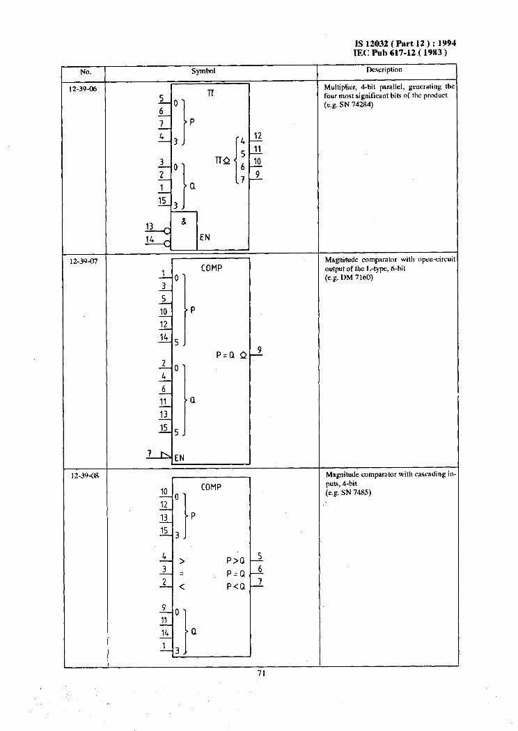
IS 12032 ( Part 12 ) : 1994 IEC Pub 617-12 ( 1983 )
No. 1 Symbol Description
12-39-06 l-l
Multiplier, d-hit parallel, generating the
four most significant bits of the product
(e.g. SN 74284)
P
d
lTQ 511
610
Q 4
13 &
14 EN
12-39-07 Magnitude comparator with open-circuit
COMP output of the L-type, 6-bit
(e.g. DM 7160)
12-39-08
' &EN
Magnitude comparator with cascading io
COMP put?, 4-bit
(e.g. SN 7485)
:
-b P>Q -ii 3 3:
A<
71

IS 12032 (Part 12 ) : 1994 IEC Pub 617-12 ( 1983 )
No.
12-39-W
12-39- 10
Symbol
COMP
P>OVL
P<QVB
P=OVJ
P?l=QV~
Magnitude comparator with 3-~&k oul
puts, 4-bit
(e.g. DM 7hL24)
Arithmetic logic unit, 4-U
(e.g. SN 74181)
Notes I. -
72

IS 12032 ( Part 12 1: 1994 IEX Pub i17-12 ( l,983 )
No.
12-39-11
Symbol
yl A- PO xi- 71; 5
QO 160
3 Pl 16 b J
Ql 160
2 P2 l;f
Q2 160 0 f
J- P3 1803 160 5 -!
Description
Arithmetic logic unit with output latches, 4-hit
(e.g. F 100181)
The notes with symbol 1239-10 apply.
SECTION 40 - BINARY DELAY ELEMENTS
40.1 The qualifyiq symbol 0508-05 is also used ia the representation of bimry delay eleruellts 8s
NO.
shown in this section.
1 Symbol
12-40-O I
4+-
Description
Delay element with specified delay times
A transition from the internal O-state to the internal 1-shle 11 Ihr:
output occurs after a delay of II with reference to Ihe same
transition at the input. The transition from the internal I-state to
the internal O-state at the output occurs after a delay of 12 wilh
reference to the same transition at the input.
A&. - 11 and 12 may be replaced by the actual delays. expressed
in seconds. or unitsor digit units. and may be placed inside
word outside the outline. If the IWO delays are equal. it is
sufficient lo insert one value only.
lllrrstrdon
b
12-40-O: IMay element (I 00 11s)
73

IS 12032 ( Part 12 ) : 1994 IEC: Pub L17-12 ( 1983 )
No. Symbol
12-40-03
Description
Tapped delay element (in steps of 10 ns)
SECTION 41- BISTABLE ELEMENTS
41.1 The sylnbol for a bistable eletneut does not contain a general qualifying synlbol for the function, the latter being indicated by qualifying synlbols associated with the inputs and outputs.
41.2 For bistable elelneuts controlled by Cn&puts (symbol 12l&01), it is necessary to distinguish between four types, i.e. latches, edge-triggered bistables, pulse-triggered bistables and data-lock- out bistables. III accordance with the descriptions of the synlbols for a dynamic input (12-07-07) and for a postponed output (12-09-01):
r --- 1
--I Cm I-
L-_-J
indicates a latch
indicates an edge-triggcrcd bistablc
indicates a pulse-triggered bistablr
r _ --_ 1
--Pm ll- indicates ;I di~Ia-lock-<~ut bistahlc
I-____A
1
For rdgc-triggcrcd, pulse-triggered ad dilti~-lock-ouI hisI;lhles, the inpuis ;~ffectcd by lhr Cm-input iire ;ISSUIW~ IO be slahle during the period thaI the Cnvinput SI;III~S ilI its iutcruill l- SlillC. If lhcy do ChilIlgC lhcir SlillCS during lhis period, lhc funclioo of lllc rlclllclll is IlO1 spcc’ificd by 1 hr symbol.
74

IS 12032 ( Part 12 ) : 1994 IEC Pub 617-12 ( 1983 )
The same symbology is used for more complex elements such as shift registers and COUI~~C~S to
indicate whether they are of the edge-triggered, the pulse-triggered or the data-lock-out type. For elements of the pulse-triggered or the data-lock-out type, if reference is made to the content of the element (e.g. by a CT- output), this content shall be considered as being the content after the application of the postponed output symbol.
SECTION 42 - EXAMPLES OF BISTABLE ELEMENTS
No.
12-42-01
12-42-02
12-42-03
12-42-04
12-42-05
12-42-06
Symbol Description
RS-histable RS-latch
D-latch, dual (e.g. part of SN 7475)
Edge-triggered JK-bistable (e.g. part of SN 74LSlO7)
Pulse-triggered JK-histable (e.g. part of SN 74107)
Data-lock-out JK-b&able (e.g. part of SN 74111)
RS-latch with nedpIed inputs (R: s - latch) (e.g. part of SN 74279)

ISl2032( Part It-):1994 IECPub 617-12((1983)
No.
12-42-07
SymhA Description
Edge-triggered D-histahle
(e.g. part of SN 7474)
12-42-08 l3 hs
Pulse-triggered RS-histahle
(e.g. SN 74L7 1)
3
4 A &
IS18 * 5 .
I2 Cl 9 t
lo '. g ,R 11 6
11
2 I\R
,'
12-42-04 Edge-triggered D-bistahle, dual
-J?-Zl
(e.g. MC 10131)
1 2s
ly
f2D G2 ’ j_’
--I )’ >c2
4R 12. 10 15
11
l3_
I2-42- 10 Edge-triggered D-histahle
(e.g. MC’ 1222)
76
,
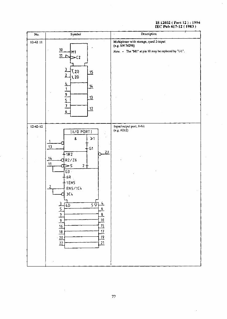
IS 12032 ( Part 12 ) : 1994 IEC Pub 117-12 ( 1983)
, 1
No. Symbol Description
12-42.11 1 Multiplexer with storage, quad 2-input
lo Ml "
(e.g. SN 74298)
Note. - The “Ml” at pin 10 mry be replaced by “Gil”.
” h>c2
1 r-
%q 15 21,2d
L'
J_ 14
9 -
Js_ _lJ
f' 12
$_
12-42-12 input/output port, R-hit
(e.g. X212)
77

IS 12032 ( Part 12 ) : 1994 IEC Pub 617-12 ( (1983 )
SECTION 43 - INDICATION OF SPECIAL SWITCHING PROPERTIES OF BISTABLE ELEMENTS
43.1 In some applicatious (e.g. fail-safe systems) it is necessary to iudicate the interual logic state of the outputs of a bistable element at the momeut the supply is switched ou. The symbols below show how this may be done. The qualifyiug symbols may be applied to other types of histablc elements.
No. Symbol Description
12-43-01 RS-histable with initial O-state
I q o At the moment the supply is switched on, the output will stand
s
0
at its internal O-state.
R
12-43-02
sl-
KS-histahle with initial l-state
I=1 At the moment the supply is switched on, the output will stand
S at its internal l-state.’
R
12-43-03
NV S
0
RS-histable, non-volatile
At the moment the supply is switched on, the internal logic state of the output will bc the same as it wax when the supply was switched off.
R
No.
12-44-01
SECTION 44 - MONOSTABLE ELEMENTS
Symbol Description
Et-
Monostahle; retriggerahle (during the output pulse). gcncral
J-L symlrrl
Simple shot, general symhool
The output changes to or remains at its 1 -state each time the inpul changes to its l-state. The output rcturus to its 0-state after ir period of time which is characteristic of the particular device. beginning at the last change of the input to its l-state.
N&r. - The useofthedynanric input synrbol(12-07-07);~ IIK input is optional (for example of use see synrlwl IL-45-01).
12-44-02 Mono&He, non retriggerahle (during the output pulse). gcncral
symbol
The output changes to its I-state only when the input ch;~ngcs 1t1 its l-state. The output returns to its O-hIilk after a period of tinic which is characteristic of the particular dcvicc, rcgardlchx of any changes of the input variable during II& period.
Nr,/c. - ‘lhc use of tllc dynamic input synllwl (syn~lwl I.?-(IT-(17) al the input is optional (for cxamplc of use v:c ~ynllx~l
12-45-02).
7x

IS 12032 ( Part 12 ) : 1994 IEC Pub 617-12 ( 1983 )
NO.
12-45-O 1
12-45-02
12-46-o I
12-46-02
SECTION 45 - EXAMPLES OF MONOSTABLE ELEMENTS
Symbol
J-L cx RX/CX
13
4
Description
Monostahle, retrigerable
(e.g. part of SN 74LS123)
Function table:
-LH LH
LIH J-L-U IHH nU
L I-l I I n u
Note. - The second and third line of the function table each
indicate the logic levels the outputs will take on after lhe
completion of any output pulse started before the relevant
input took on its indicated level.
Monostable, non-retriggerable
(e.g. part of SN 74221)
SECTION 46 - ASTABLE ELEMENTS
Symbol
Lt rl5-L
a
Description
,Astahle elementt general symbol
Signal generator producing an alternatillgscquencr:ofzcrocs and
ones.
Nofe. - In this symbol. the G is the qualifying symbol for a
generator. If the waveform is evident. this symbol may he
shown without the additional symbol M
Controlled astahlc element, general symbol
a- ‘l‘hc note with symbol 12-46-01 applies.

IS 12032(1%1rt12):1YY4 IIS1 Pub 617-12 ((lYS3)
No. Symlwd
12-46-03
D-
J--S_
Dcsrriplion
Astable element, synchronoudy starting, general symbol
, The output starts with a complete pulse at the inst;lnt ;II which the input takes m i$ internal l-state.
Input b r----
oulput :, d-uLrL:~TII
12-46-04
The note with hyml~ol 12-46-Oi applies.
Astable elemcnl stopping after cnmplctinp the last pulse, general
G!
,iz+
symbol
When the input returns to ils internal O-state, Ihe output remains at its’internal 0-slale or completes its linal pulse.
Input 1 0 -----j-
outpu1 ‘0 TI:InniL_
The note with symbol 12-46-01 applies.
- 12-46-05 Astahleelement, synclironously starting, stoppingaller romplet
!G!
-E+
ing the last pulse, gCllCrill symbol
Inpu1 ; J-L
I I
Outpul (QLnmlh
The nole with symbol 12-46~1 applie:,.
so

IS 12032 ( Part 12) : 1994 IEC Pub 617-12 ( 1983 )
SECTION 47 - EXAMPLES OF ASTABLE ELEMENTS
Note. - For the use of CTRDIV4 see sym
bol 12-48-03.
N&z - If it is not necessary to detail the
supply arrangements. the common
control block may be omitted.

IS 12032 ( Part 12 ) : 1994 IEC Pub 617-12 ((1983)
NO.
12-a-01
12-48-02
12-48-03
NO.
12-49-01
12-49-02
SECTION 48 - SHIFT REGISTERS AND COUNTERS
Description
Shift register, general symbol
NOEL’. - ‘lbe nl must he replaced by the number of stages.
Counter with cycle Icngth 2 to the power m (counter module 2
to the power m), general symbol
No/e. - m should he replaced hy the actual value.
Counter wi th cycle length m (counter modulo m), general symlx~l
The note with symbol 12-48-02 applies.
NO/L’. - In an array of elements having different cycle lengths. that
applyq to each should he indicated by DIVm in each
elen~en~. In such a case. the letters (TR need only bc
shown in the common control block (for example of
applicalion see symbol 12-49-12).
SECTION 49 - EXAMPLES OF SHIFT REGISTERS AND COUNTERS
Symbol
SRGB
SRG512
1 Ml a t 3,1,2D 23 3 2 i,2D 5 c2/+
-
Description
Shift register, R-bit, with serial input and complementary serial
output
(e.g. part of SN 749 1)
Shift register, 512~bit, static
(e.g. MM 4057)
1
82

IS12032 (Fart 121 :1994 IEC Ful,L17-12( i983)
NO. Symbol Ikscription
12-49-03 Shift register, 4-bit, bidirectional universal
9 -0
SRG4 (e.g. SN 74lS 194)
10 , M; - 1
11 .>c4
L-l-WC
1R
7 -L 1,4D
r
15
3 3,4D
L3,4D -2
?- 3,4D p 13
6 3,4D 12
f 2,4D
12-49-04
7r\ SRG4
Ml 6
>c2/1--
2 KN, S
R-
Shift register, 4-M, parallel in/parallel out
(e. f. CD 4035A)
Note. - The use of the bar can be avoided by replacing
-Ml hy I Mo and T by 0. I-eL MI
4 1 r 1.2J
3 r\1,2K 31 9
i,2D
12-49-05 Shift register, 8-hil, with parallel oulpulh
(e.g. SN 74164)
8 SRG8
>Cl/+
9R
_g I-
_2_ & 1D 3
-4
* 5
-6
-2
’ 11
~ 12
~ 13
x3

I .
IS12032(Part12):.1994 IECPub 617-12 ((1983) . . _
No. Symbol Description
t-49-06 Shift register with parallel load, S-hit
SRG8 (e. g. SN 74 165)
1
I <G'isH'FT1 CZILOADI l
15 >' J_ l>W--,
y-l 1030
r
i-20 E2D
14
3
1,'
5 .
6, - 9
\!
12-49-07 1 Register, universal shift/storrgee, 8-hit (e.g. SN 74lS323) l’or
12 SRG8 which only the reset, shift and parallel load modes are shown.
>c3/13
9 No/c. - 711is symbol illuelr:Ws how an inronlpiclcly ulilizcd
b3RIRESETl dcvicc may bc rcprcscnlcd by :I synllwl suited IL) 111~
19 .&
I MltSHIFTI
application. For this purpose USC is nladc ol IIKZ l’ixcd-
mode input. symbol IL- 09-49.
A MZ[LOADI _l_ ","
_2_ ","
3 ” ,”
1 %,3D
r
f 2,3D
F 2,3D
14'
5
15' 1,
16 - 17 ,
x4

IS 12032 ( Part 12 ) : 1994 IEC Pub 617-12 ( 1983 )
NO. Description
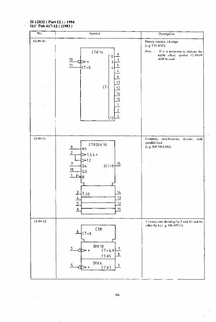
is 12032 ( Part 12 ) : 1YY4 IEC Pub 617-12 ( (1983 )
NO
2-49- 10
2-4% 11
12-49-12
Symlwl
10 11
CTR14
>+
:T=O
CT
‘0 9 3 ?
4 5 4
6
13
I
12
14
15
1
2
13 3
9 CTRDlVlO
Ml 2
.>1,3,4 +
L,,2 7
*G4 3cr=9
lo G3
'hR
15 -
CTR
d+ D'V6CT>,3 k
13inary counter, I4-slagc (Lg. (‘I) 4020)
hr,le. - II it ia nccessnry 10 indir;hlc the ripple ctkrt. symbol 12-49-09 shall hc used.
Counters, syncllrcvlous. dccadl~. with
parallel load
(e.g. SN 741s 1.50)
(‘wntcr, one dividing hy 5 and IO ;IIIJ 111 other hy 6 (c. g. SN 4971 I)
Sh

IS 12032 ( Part 12 ) : 1994 IEC Pub 617-12 ( 1983 )
Description
Decade counter/divider with decoded 7-
segment display outputs
(e.g. CD 4026)
Segment identification:
fLb e I c
d
No.
12-49-13
Symbol
CTRDIVlO/fSEG 1o al2.
2 b2
bl2 - ”
’ JT>+
cl2 13
d12, 9
” ,CT=O el2. "
f12 ;
912 CL '4
CT>5 1 '
%Gl2 1 4
12-49-14 Counter, decade, synchronous up/down
CTRDIVlO (e.g. SN 74192)
‘lr -R 5 ,>2+
LGl
iCT=9C)--12
4 >l-
LG2
%T=O0--ll
11c3
-3_ y3D 2
10 6
9 7
12-49-15 Binary counter, 4-hit, synchronous up/down, shown with supplementary
4 hEN1 CTR4 clarifying information in the array
(e.g. SN 74191)
5 !!??(DOWNI 2(CT=O)Z6 ”
I bM3IUPI 31CT=151Zb--I 14 %,2-/1,3+
I r\ G4 11
6,4,1 ' l3 r\C5[LOADl
10 141
6
_!I_ I81
‘L
87

IS 12032 ( Part 12 ) : 1994 IEC Pub 617-12 ( (1983 )
No. Symbol
12-49-16
Description
Counter, decade
(e.g. part of SN 74490)
SECTION 50 - MEMORIES
No.
L2-SO-01
Symbol Description
Read-only memory, general symbol
Note. - The asterisk must be replaced by an appropriate indication
of the number of addresses and bit. In such indications lk
stalrds for 1024.
Programmable read-only memory, general symbol
The note with symbol 12-50-01 applies.
12-50-03 Random-access memory (read/write memory), general symbol
The note with symbol 12-50-01 applies.
Content addressable memory (associative memory). ge:ener;i
symbol
The note with symbol 12-5041 applies.
88