is2008s - ww1.microchip.com
TRANSCRIPT
Brochure
IS2008S
Bluetooth 4.1 Mono Audio SOC
Phone: 886-3-577-8385 Website: www,issc-tech.com Draft 0.92 6
th Oct, 2014
GENERAL DESCRIPTION
IS2008S is a compact, highly integrated,
CMOS single-chip RF and baseband IC for
preliminary Bluetooth v4.1 with Enhanced
Data Rate 2.4GHz applications. This chip is
fully compliant with Bluetooth specification
and completely backward-compatible with
Bluetooth 3.0, 2.0 or 1.2 systems.
It incorporates Bluetooth 1M/2M/3Mbps
RF, single-cycle MCU, MODEM, UART
interface, and ISSC’s own Bluetooth software
stack to achieve the required BT v4.1 with
EDR functions.
To provide the superior audio and voice
quality, it also integrates a DSP co-processor, a
PLL, and a CODEC dedicated for voice and
audio applications.
For voice, not only basic CVSD encoding
and decoding but also enhanced noise
reduction and echo cancellation are
implemented by the built-in DSP to reach the
better quality in the both sending and receiving
sides. For enhanced audio applications,
SBC/AAC_LC decoding functions can be also
carried out by DSP to satisfy Bluetooth A2DP
requirements.
In addition, to minimize the external
components required for portable devices, a
voltage sensor for battery, battery charger, a
switching regulator and LDO are integrated to
reduce BOM cost for various Bluetooth
applications.
BQB QUALIFICATION LISTING
B022584: BT4.1 component
B021155: Profiles components
FEATURES
Support preliminary Bluetooth v4.1
function and backward compatible with
BT3.0, 2.0 and 1.2.
ISSC’s own Bluetooth software stack for
the headset or speaker application. It
supports following profiles :
- Hands Free 1.6
- Headset 1.1
- A2DP 1.2
- AVRCP 1.5
Integrated a DSP core that supports:
- Noise suppression
- Echo suppression
- SBC/AAC_LC audio format decoding
- Automatic volume control for mono
speaker output
Integrated a 20-bit audio CODEC that
SNR ( A-weighted) over 94dB for DAC
and 88dB for ADC
Connection to two phones with
HFP/A2DP profiles
Built-in four languages ( Chinese/
English/ Spanish/ French) voice prompts
Low power consumption under 10mA for
SCO/A2DP link ( no loading)
Capable charging voltage from an empty
battery and sustain a direct DC input
voltage up to 7V
Charging current up to 250mA
6 mm x 6 mm QFN 48 package
APPLICATIONS
Bluetooth mono headset with A2DP
music streaming
Bluetooth mono speaker
Bluetooth mono speaker phone
Bluetooth mono car audio unit

Brochure
IS2008S
Bluetooth 4.1 Mono Audio SOC
Phone: 886-3-577-8385 Website: www,issc-tech.com Draft 0.92 6
th Oct, 2014
Table of Contents
1 KEY FEATURES ................................................................................................................................................ 3
2 PIN ASSIGNMENTS .......................................................................................................................................... 6
3 TRANSCEIVER .................................................................................................................................................. 9
4 MICROPROCESSOR ...................................................................................................................................... 10
5 AUDIO ............................................................................................................................................................... 11
6 POWER MANAGE UNIT ................................................................................................................................ 12
7 GENERAL PURPOSE IOS .............................................................................................................................. 14
8 SPECIFICATIONS ........................................................................................................................................... 15
9 PACKAGE ......................................................................................................................................................... 27

Data Sheet
IS2008S
- 3 -
1 Key Features
System Specification
Compliant with Bluetooth Specification v.4.1 (EDR) in 2.4 GHz ISM band
Baseband Hardware
16MHz main clock input
Built-in internal ROM for program memory
Support to connect to two hosts ( phones, tablets…) with HFP or A2DP profiles
simultaneously
Adaptive Frequency Hopping (AFH) avoids occupied RF channels
Fast Connection supported
RF Hardware
Fully Bluetooth 4.1 (EDR) system in 2.4 GHz ISM band.
Combined TX/RX RF terminal simplifies external matching and reduces external
antenna switches.
Max. +4dBm output power with 20 dB level control from register control.
Built-in T/R switch for Class 2/3 application
To avoid temperature variation, temperature sensor with temperature calibration is
utilized into bias current and gain control.
Fully integrated synthesizer has been created. There requires no external VCO,
varactor diode, resonator and loop filter.
Crystal oscillation with built-in digital trimming for temperature/process variations.
Audio processor
Support 64 kb/s A-Law or -Law PCM format, or CVSD (Continuous Variable Slope
Delta Modulation) for SCO channel operation.

Data Sheet
IS2008S
- 4 -
Noise suppression
Echo suppression
SBC/AAC decoding
Packet loss concealment
Build-in four languages (Chinese/ English/ Spanish/ French) voice prompts and 20
events for each one
Audio Codec
94dB SNR DAC playback
Integrate headphone amplifier for 16/32Ω speakers
Wideband Speech
Support mSBC speech en/decoders for high-definition speech quality
Peripherals
Built-in Lithium-ion battery charger
Integrate 3V, 1.8V LDO and Switching mode regulator
Built-in ADC for battery monitor and voltage sense.
Two LED drivers
Flexible HCI interface
High speed HCI-UART (Universal Asynchronous Receiver Transmitter) interface
Package
6x6mm2 48QFN package

Data Sheet
IS2008S
- 5 -
APPLICATION DIAGRAM
BT BDR/EDR
Radio transceiverMCU
DSPRAM/ROM CODEC
PMU
Clock PLL
EEPROM

Data Sheet
IS2008S
- 6 -
2 PIN ASSIGNMENTS
1
2
3
4
36
35
34
33
5
6
7
8
9
10
11
12
32
31
30
29
28
27
26
25
13 14 15 16 17 18 19 20 21 22 23 24
373839404142434445464748
IS2008S

Data Sheet
IS2008S
- 7 -
Pin No. I/O Pin Name Pin Descriptions
1 P VCOM Internal biasing voltage for CODEC
2 P NC No connect
3 P NC No connect
4 I MICN1 Mic 1 mono differential analog negative input
5 I MICP1 Mic 1 mono differential analog positive input
6 P MIC_BIAS Electric microphone biasing voltage
7 P VDD_CORE Core 1.2V power input
8 P P1_2 GPIO, default pull-high input
9 I/O P1_3 GPIO, default pull-high input
10 I/O RST_N System Reset Pin
11 AI VDD_IO I/O power supply input
12 I/O P0_1 GPIO, default pull-high input
13 I/O P1_5 GPIO, default pull-high input
14 I HCI_RXD HCI RX data
15 O HCI_TXD HCI TX data
16 P CODEC_VO 3.1V LDO output for CODEC power
17 P LDO31_VIN 3.1V LDO input
18 P LDO31_VO 3.1V LDO output
19 P ADAP_IN Power adaptor input
20 P BAT_IN Battery input
21 AI AMB_DET ADC analog input 1
22 AI SAR_VDD SAR 1.8V input
23 P SYS_PWR System Power Output
24 P BK_VDD Buck VDD Power Input
25 P BK_LX Buck feedback input
26 P BK_OUT Buck output
27 I PWR Multi-Function Push Button key
28 P LED2 LED Driver 2
29 P LED1 LED Driver 1
30 I/O P0_3 GPIO, default pull-high input
31 P CLDO_O 1.2V core LDO output
32 P PMIC_IN PMU blocks power input.
33 P RFLDO_O 1.28V RF LDO output
Data Sheet
IS2008S
- 8 -
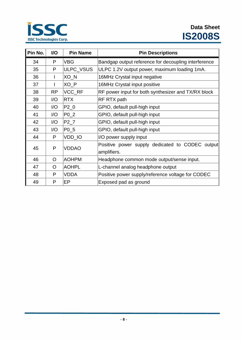
Pin No. I/O Pin Name Pin Descriptions
34 P VBG Bandgap output reference for decoupling interference
35 P ULPC_VSUS ULPC 1.2V output power, maximum loading 1mA.
36 I XO_N 16MHz Crystal input negative
37 I XO_P 16MHz Crystal input positive
38 RP VCC_RF RF power input for both synthesizer and TX/RX block
39 I/O RTX RF RTX path
40 I/O P2_0 GPIO, default pull-high input
41 I/O P0_2 GPIO, default pull-high input
42 I/O P2_7 GPIO, default pull-high input
43 I/O P0_5 GPIO, default pull-high input
44 P VDD_IO I/O power supply input
45 P VDDAO Positive power supply dedicated to CODEC output
amplifiers.
46 O AOHPM Headphone common mode output/sense input.
47 O AOHPL L-channel analog headphone output
48 P VDDA Positive power supply/reference voltage for CODEC
49 P EP Exposed pad as ground

Data Sheet
IS2008S
- 9 -
3 TRANSCEIVER
IS2008S is design optimized for use in Bluetooth 2.4 GHz system. It contains a complete
radio frequency transmitter/receiver section. An internal synthesizer generates a stable clock for
synchronize with another device.
TRANSMITTER
The internal PA has a maximum output power of +4dBm with level control 20dB from
amplitude control. This is applied into Class2/3 radios without external RF PA.
The transmitter features IQ direct conversion to minimize the frequency drift. And it can
excess 30dB power range with temperature compensation machine.
RECEVIER
The LNA operates with TR-combined mode for single port application.
The ADC is utilized to sample input analogue wave to convert into digital for de-modulator
analysis. Before the ADC, a channel filter has been integrated into receiver channel that can reduce
the external component count and increase the anti-interference capability.
The image rejection filter is to reject image frequency for low-IF architecture. This filter for
low-IF architecture is implied to reduce external BPF component for super heterodyne
architecture.
There is an RSSI signal to the processor that it can control the power to make a good tradeoff
for effective distance and current consumption.
SYNTHESIZER
A synthesizer generates a clock for radio transceiver operation. There is a VCO inside with
tunable internal LC tank. It can reduce variation for components. A crystal oscillation with internal
digital trimming circuit provides a stable clock for synthesizer.
MODEM
On the Bluetooth v1.2 specification and below, 1 Mbps was the standard data rate based on
Gaussian Frequency Shift Keying (GFSK) modulation scheme. This basic rate modem meets BDR
requirements of Bluetooth v2.0 with EDR specification.
On the Bluetooth v2.0 with EDR specification, Enhanced Data Rate (EDR) has been
introduced to provide 2 and 3 Mbps data rates as well as 1 Mbps. This enhanced data rate modem
meets EDR requirements of Bluetooth v2.0 with EDR specification. For the viewpoint of baseband,
both BDR and EDR utilize the same 1MHz symbol rate and 1.6 KHz slot rate. For BDR, 1 symbol
represents 1 bit. However each symbol in the payload part of EDR packets represents 2 or 3 bits.
This is achieved by using two different modulations, π/4 DQPSK and 8DPSK.

Data Sheet
IS2008S
- 10 -
4 MICROPROCESSOR
A single-cycle 8-bit MCU is inside IS2008S to carry out the required Bluetooth protocols. It
can run at the range from 16MHz to a higher clock so that MCU firmware can dynamically
consider the tradeoff between computing power and power consumption. MCU firmware is
implemented in ROM (Read-Only-Memory) to minimize the power consumption of program
execution and to save the cost of external flash.
MEMORY
A single-port synchronous interface is provided to memory. There are enough ROM and
RAM to fulfill the requirement of processor. In addition, attached to the embedded processor bus
are a register bank, a dedicated single-port memory, and flash memory. The processor coordinates
all link control procedures and data movement using a set of pointer registers.
EXTERNAL RESET
A watchdog timer capable of reset the chip. It has an integrated Power-On Reset (POR)
circuit that resets all circuits to a known power-on state. This action can also be driven by an
external reset signal that can be used to externally control the device, forcing it into a power-on
reset state. The RST signal input is active low and no connection is required in most applications.
REFERENCE CLOCK
IS2008S is composed of an integrated crystal oscillation function. It used a 16 MHz external
crystal and two specified load capacitors that a high quality system reference timer source is
obtained. This feature is typically used to remove the initial tolerance frequency errors associated
with the crystal and its equivalent load capacitance in mass production. Frequency trim is achieved
by adjusting the crystal load capacitance through on-chip trim capacitors Ctrim integrated in chip.
The value of trimming capacitance is around 200fF per LSB at 5 bits word, therefore the
overall adjustable clock frequency is around 40 KHz.
trimC =200fF * (1~31)
IS2008S
XO_N XO_P
CL CL

Data Sheet
IS2008S
- 11 -
5 AUDIO
There are several stages for input and output that all can be programmed for varying gain
response characteristics. At the microphone input side, you may use single-end input or differential
input. One critical point in maintaining a high quality signal is to provide a stable bias voltage
source for the condenser microphone’s FET. DC blocking capacitors may be used at both positive
and negative sides of input. Internally, this analog signal is converted to 16-bit 8 kHz or 16 kHz
linear PCM data formats for conventional CVSD and wide-band speech codecs, respectively.
The voice data taken from common memory is converted to an analogue value by a DAC. A
multistage amplifier drives the audio signal and provides a differential signal between Line_out+
and Line_out-. The output amplifier is capable of driving a speaker directly if its impedance is
16/32Ω.
DIGITAL SIGNAL PROCESSOR
A digital signal processor (DSP) cooperates with MCU to deal with audio section. It provides
audio processing with some advanced features. The DSP includes the capability to cancel the
acoustic echo that may be present in a headset or speaker. All processing is performed by a DSP
with low power consumption. This technique will most effectively cancel the incoming echo
signal without impact to the desired voice signal. An outgoing signal to the speaker which level
exceeds a certain threshold (and therefore deemed likely to create echo) will result in suppression
of signal along the input path from the microphone. Filtering is also applied and provides for a
smoother transition for a more natural user experience.
CODEC
This built-in codec contains a high Signal/Noise performance. This built-in codec contains a
analog to digital converter (ADC), a digital to analog converter (DAC) and additional analog
circuitry.
Signal to noise ratio (SNR) is the supreme facts of a CODEC. It provides a very low noise
level for background white noise. The main music stream and vocal become clear with this low
noise level.

Data Sheet
IS2008S
- 12 -
6 POWER MANAGE UNIT
The PMU inside the chip has two main features, charging a Li-ion battery and some regulators
for voltage translation. A power switch is used to switch over the power source between battery
and adaptor automatically. It also provides two LED drivers.
CHARGING A BATTERY
IS2008S includes a built-in battery charger optimized for use with lithium polymer batteries.
The charger features a current sensor for charging control, user programmable current regulation
and high accuracy voltage regulation.
The charging current is configured in the EEPROM. Whenever the adaptor is plug-in,
charging circuit is active. Reviving, Pre-charging, Constant Current and Constant Voltage modes
are implemented and re-charging function is also included. The maximum charging current is
250mA.
Charging curve
Precharge Voltage
2.5v
CC Voltage 3.0v
CC current 0.5c
Recharge Voltage
4.1v
CV Voltage 4.2v Constant Current Mode Constant Voltage Mode
Recharge
ModePre charge
Mode
Reviving
Mode
Reviving Current
2mA
Precharge Current
0.1c
Recharge current
0.25c
VOLTAGE MONITING
A 10-bit Successive-Approximation-Register analog to digital converter (SAR ADC) provides
one dedicated channel for battery voltage level detection. The warning level is programmable and
stored in the EEPROM. This ADC provides a good resolution that MCU can control the charging
process.
VOLTAGE REGULATION
The built-in voltage converter is used to convert the battery or adaptor power for power
supply. It also integrates hardware architecture to control power on/off procedure. The built-in
programmable LDOs provide power for codec and digital IO pads. It is used to buffer the high

Data Sheet
IS2008S
- 13 -
input voltage from battery or adapter. This LDO need s 1uF bypass capacitor.
SWITCHING REGULATOR
There is a bulk voltage convert generating the voltage for RF and baseband core power. This
converter has good conversion efficiency to save power and fast transient response.
LED DRIVER
There are two dedicate LED drivers to control the LEDs. They provide enough sink current
that LED can be connected directly with IS2008S.
IS2008SLED1
LED2
SYS_PWR

Data Sheet
IS2008S
- 14 -
7 GENERAL PURPOSE IOs
IS2008S provides six general purpose IOs for keys setting and saved in the EEPROM. The
first button must be power key. The power on/off functions only can be set on MFB pin. There are
four different operations for every button. They are short click, long click, double click and
combinations.
GPIOs for Buttons
Button Name Default Functions GPIO name Pin
Button 0 Power / MFB MFB 27
Button 1 PLAY/PAUSE P0_2 40
Button 2 Volume UP P2_7 42
Button 3 Volume DN P0_5 43
Button 4 FWD P0_1 12
Button 5 REV P0_3 30
Some signals were generated to indicate or control outside devices. The most popular
applications are NFC for easy pairing, external audio amplifier for louder speaker and buzzer for
indication.
GPIOs for added functions
Functions GPIO name Pin
Slide switch P1_5 13
Buzzer P20 30
NFC detect P1_5 13
External AMP enable P1_5 13
Data Sheet
IS2008S
- 15 -
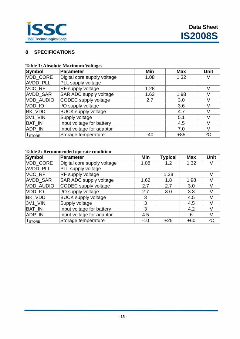
8 SPECIFICATIONS
Table 1: Absolute Maximum Voltages
Symbol Parameter Min Max Unit
VDD_CORE AVDD_PLL
Digital core supply voltage PLL supply voltage
1.08 1.32 V
VCC_RF RF supply voltage 1.28 V
AVDD_SAR SAR ADC supply voltage 1.62 1.98 V
VDD_AUDIO CODEC supply voltage 2.7 3.0 V
VDD_IO I/O supply voltage 3.6 V
BK_VDD BUCK supply voltage 4.7 V
3V1_VIN Supply voltage 5.1 V
BAT_IN Input voltage for battery 4.5 V
ADP_IN Input voltage for adaptor 7.0 V
TSTORE Storage temperature -40 +85 ºC
Table 2: Recommended operate condition
Symbol Parameter Min Typical Max Unit
VDD_CORE AVDD_PLL
Digital core supply voltage PLL supply voltage
1.08 1.2 1.32 V
VCC_RF RF supply voltage 1.28 V
AVDD_SAR SAR ADC supply voltage 1.62 1.8 1.98 V
VDD_AUDIO CODEC supply voltage 2.7 2.7 3.0 V
VDD_IO I/O supply voltage 2.7 3.0 3.3 V
BK_VDD BUCK supply voltage 3 4.5 V
3V1_VIN Supply voltage 3 4.5 V
BAT_IN Input voltage for battery 3 4.2 V
ADP_IN Input voltage for adaptor 4.5 6 V
TSTORE Storage temperature -10 +25 +60 ºC

Data Sheet
IS2008S
- 16 -
Table 3: BUCK switching regulator
Parameter Min Typical Max Unit
Input Voltage 3.0 3.8 4.5 V
Output Voltage (Iload=70mA, Vin=4V) 1.7 1.8 2.05 V
Output Voltage Accuracy ±5% %
Output Voltage Adjustable Step 50 mV
/Step
Output Adjustment Range -0.1 +0.25 V
Output ripple 10 15 mVRMS
Average Load Current (ILOAD) 120 mA
Conversion efficiency (BAT=3.8V, Iload = 50mA) 88 %
Switching frequency 800 KHz
Quiescent Current 1000 μA
Output Current (peak) 200 mA
Load Regulation (Iload = 10 ~ 100mA) 1 mV/
mA
Line Regulation (3.2V < Vin < 4.2V) 0.03
(30)
%/V
(mV/V)
EN threshold Logic Low Voltage 0.4 V
Logic High Voltage 1.62 V
EN current 10 nA
Shutdown Current <1 μA

Data Sheet
IS2008S
- 17 -
Table 4: Low Drop Regulation
Parameter Min Typical Max Unit
Input Voltage 3.0 4.3 V
Output Voltage
VOUT CODEC 2.9
V
VOUT IO 1.8
Output Accuracy (VIN=3.7V, ILOAD=100mA, 27’C) ±5 %
Transient response Iload = 10 to 50mA 40 60
μs Iload = 50 to 10mA 40 60
Output current (average) 100 mA
Drop-out voltage
(Iload = maximum output current) 300 mV
Quiescent Current
(excluding load, Iload < 100μA) 45 μA
Load Regulation
(Iload = 0mA to 100mA) 40 mV
Line Regulation
(Vout+0.3V<Vin<4.5V) 7 10 mV/V
EN threshold Logic Low Voltage 0.4 V
Logic High Voltage 1.62 V
EN current 10 nA
Shutdown Current <1 μA

Data Sheet
IS2008S
- 18 -
Table 5: Battery Charger
Parameter Min Typical Max Unit
Input Voltage 4.5 5.0 7.0 V
Supply current to charger only 3 4.5 mA
Battery trickle charge current
(BAT_IN < trickle charge voltage threshold) 0.1C mA
Maximum Battery
Fast Charge Current
Note: ENX2=0
Headroom > 0.7V
(ADAP_IN=5V) 170 200 240 mA
Headroom = 0.3V
(ADAP_IN=4.5V) 160 180 240 mA
Maximum Battery
Fast Charge Current
Note: ENX2=1
Headroom > 0.7V
(ADAP_IN=5V) 330 370 420 mA
Headroom = 0.3V
(ADAP_IN=4.5V) 180 220 270 mA
Trickle Charge Voltage Threshold 3 V
Float Voltage 4.158 4.2 4.242 V
Battery Charge Termination Current,
(% of Fast Charge Current) 10 %
Note:
(1) C is set in EEPROM
(2) Headroom = VADAP_IN – VBAT
(3) ENX2 is not allowed to be enabled when VADAP_IN – VBAT > 2V
Table 6: LED driver
Parameter Min Typical Max Unit
Supply Voltage 1.7 1.8 1.98 V
Open-drain Voltage 5.1 V
Open-drain Current 5.5 mA
Intensity Control 16 step
Current Step 0.35 mA
Power Down Open-drain Current 1 μA
Shutdown Current 1 μA

Data Sheet
IS2008S
- 19 -
Table 7: Audio codec Digital to Analogue Converter
T= 25oC, Vdd=3.0V, 1KHz sine wave input, Bandwidth = 20~20KHz
Parameter (Condition) Min. Typ. Max. Unit
Over-sampling rate 128 fs
Resolution 16 20 Bits
Output Sample Rate 8 48 KHz
Signal to Noise Ratio Note: 1
(SNR @cap-less mode) for 48kHz 94 96 dB
Signal to Noise Ratio Note: 1
(SNR @single-end mode) for 48kHz 94 96 dB
Digital Gain -54 4.85 dB
Digital Gain Resolution 2~6 dB
Analog Gain -28 3 dB
Analog Gain Resolution 1 dB
Output Voltage Full-scale Swing (AVDD=2.8V) 495 742.5
mV rms
Maximum Output Power (16Ω load) 15.3 34.5 mW
Maximum Output Power (32Ω load) 7.6 17.2 mW
Allowed Load (Resistive) 8 16 O.C. Ω
THD+N (16Ω load) 0.05 %
Signal to Noise Ratio (SNR @ 16Ωload) 96 dB
Note: (1) fin=1KHz, B/W=20~20KHz, A-weighted, THD+N < 0.01%, 0dBFS signal,
Load=100KΩ

Data Sheet
IS2008S
- 20 -
Table 8: Audio codec Analogue to Digital Converter
T= 25oC, Vdd=3.0V, 1KHz sine wave input, Bandwidth = 20~20KHz
Parameter (Condition) Min. Typ. Max. Unit
Resolution 16 Bits
Output Sample Rate 8 48 KHz
Signal to Noise Ratio Note: 1
(SNR @MIC or Line-in mode)
8KHz 86 88
16KHz 86 88
32KHz 86 88
44.1KHz 85 87
48KHz 85 87 dB
Digital Gain -54 4.85 dB
Digital Gain Resolution 2~6 dB
MIC Boost Gain 20
Analog Gain 60 dB
Analog Gain Resolution 2.0 dB
Input full-scale at maximum gain (differential) 4 mV rms
Input full-scale at minimum gain (differential) 800 mV rms
3dB bandwidth 20 KHz
Microphone mode (input impedance) 6 10 KΩ
Microphone mode (input capacitance) 20 pF
THD+N (microphone input) @30mVrms input 0.02 %
Note: (1) fin=1KHz, B/W=20~20KHz, A-weighted, THD+N < 1%, 150mVpp input

Data Sheet
IS2008S
- 21 -
Table 9: Transmitter section for BDR
Parameter Min Typ Max Bluetooth
specification Unit
Maximum RF transmit power 3 4.0 -6 to 4 dBm
RF power variation over
temperature range with
compensation disabled
±3.0 dB
RF power control range 18 ≥16 dB
RF power range control resolution ±0.5 dB
20dB bandwidth for modulated
carrier 900 ≤1000 KHz
ACP
Note:
F0=2441MHz
F = F0±2MHz -28 -26 ≤-20 dBm
F = F0±3MHz -43 -43 ≤-40 dBm
F = F0±>3MHz -54 -53 ≤-40 dBm
∆f1avg maximum modulation 150 165 140<∆f1avg<175 KHz
∆f2max maximum modulation 120 140 ≥115 KHz
∆f2avg/∆f1avg 0.92 0.94 ≥0.80
ICFT 4.5 8 10.5 ±75 KHz
Drift rate 3.3 7.0 ≤20 KHz/5
0us
Drift (single slot packet) 12 ≤40 KHz
2nd harmonic content -53 ≤-30 dBm
3rd harmonic content -55 ≤-30 dBm

Data Sheet
IS2008S
- 22 -
Table 10: Transmitter section for EDR
Min Typ Max Bluetooth
specification Unit
Relative transmit power -1.4 -4 to 1 dB
π/4 DQPSK max
carrier frequency
stability
|ωo|
freq. error 2.5 5 ≤10 for all blocks KHz
|ωi|
initial freq.
error
2.5 5 ≤75 for all blocks KHz
|ωo+ωi|
block freq.
error
5 10 ≤75 for all blocks KHz
8DPSK max carrier
frequency stability
|ωo|
freq. error 2.5 5 ≤10 for all blocks KHz
|ωi|
initial freq.
error
2.5 5 ≤75 for all blocks KHz
|ωo+ωi|
block freq.
error
5 10 ≤75 for all blocks KHz
π/4 DQPSK
modulation
accuracy
RMS DEVM 7 ≤20 %
99% DEVM PASS ≤30 %
Peak DEVM 25 ≤35 %
8DQPSK
modulation
accuracy
RMS DEVM 7 ≤13 %
99% DEVM PASS ≤20 %
Peak DEVM 20 ≤25 %
In-band spurious
emissions
Note: F0=2441MHz
F >
F0+3MHz <-52 ≤-40 dBm
F <
F0-3MHz <-53 ≤-40 dBm
F =
F0-3MHz -46 ≤-40 dBm
F =
F0-2MHz -34 ≤-20 dBm
F = -34 ≤-26 dBm

Data Sheet
IS2008S
- 23 -
F0-1MHz
F =
F0+1MHz -37 ≤-26 dBm
F =
F0+2MHz -34 ≤-20 dBm
F =
F0+3MHz -46 ≤-40 dBm
EDR differential phase encoding 100 ≥99 %

Data Sheet
IS2008S
- 24 -
Table 11: Receiver section for BDR
Frequency
(GHz) Min Typ Max
Bluetooth
specification Unit
Sensitivity at 0.1%
BER
2.402 -91
≤-70 dBm 2.441 -91
2.480 -91
Maximum received signal at 0.1%
BER 0 ≥-20 dBm
Continuous power
required to block
Bluetooth
reception (for input
power of -67dBm
with 0.1% BER)
measured at the
unbalanced port of
the balun
0.030–2.000 -10
dBm
2.000-2.400 -27
2.500-3.000 -27
3.000-12.75 -10
C/I co-channel 5 ≤11 dB
Adjacent channel
selectivity C/I
Note: F0=2441MHz
F =
F0+1MHz -7 ≤0 dB
F =
F0-1MHz -7 ≤0 dB
F =
F0+2MHz -36 ≤-30 dB
F =
F0-2MHz -22 ≤-9 dB
F =
F0-3MHz -24 ≤-20 dB
F =
F0+5MHz -50 ≤-40 dB
F = Fimage -22 ≤-9 dB
Maximum level of intermodulation
interferers N/A ≥-39 dBm
Spurious output level N/A dBm/Hz
Data Sheet
IS2008S
- 25 -
Table 12: Receiver section for EDR
Freq.
(GHz)
Modula
tion Min Typ Max
Bluetooth
specification Unit
Sensitivity at
0.01% BER
2.402 π/4
DQPSK -91 -90
≤-70 dBm 2.441 π/4
DQPSK -91 -90
2.480 π/4
DQPSK -91 -90
2.402 8DPSK -84 -83
≤-70 dBm 2.441 8DPSK -84 -83
2.480 8DPSK -84 -83
Maximum received signal at
0.1% BER
π/4
DQPSK -10 ≥-20
dBm
8DPSK -10 ≥-20
C/I co-channel at 0.1% BER
π/4
DQPSK 5 ≤13 dB
8DPSK 5 ≤21 dB
Adjacent
channel
selectivity C/I
Note:
F0=2441MHz
F =
F0+1MHz
π/4
DQPSK -13.5 ≤0 dB
8DPSK -8 ≤5 dB
F =
F0-1MHz
π/4
DQPSK -13 ≤0 dB
8DPSK -7.5 ≤5 dB
F =
F0+2MHz
π/4
DQPSK -38 ≤-30 dB
8DPSK -34 ≤-25 dB
F =
F0-2MHz
π/4
DQPSK -23 ≤-7 dB
8DPSK -21 ≤0 dB
F =
F0-3MHz
π/4
DQPSK -26 ≤-20 dB
8DPSK -19 ≤-13 dB
F =
F0+5MHz
π/4
DQPSK -53 ≤-40 dB

Data Sheet
IS2008S
- 26 -
8DPSK -46 ≤-33 dB
F = Fimage
π/4
DQPSK -23 ≤-7 dB
8DPSK -21 ≤0 dB

Data Sheet
IS2008S
- 27 -
9 PACKAGE
Chip Outline