isl95210 datasheet - intersil · pdf filehigh efficiency 5v, 10a buck regulator datasheet the...
TRANSCRIPT
FN6938Rev 4.00
December 15, 2011
ISL95210High Efficiency 5V, 10A Buck Regulator
DATASHEET
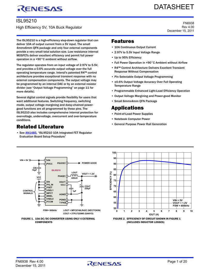
The ISL95210 is a high-efficiency step-down regulator that can deliver 10A of output current from a 5V input. The small 4mmx6mm QFN package and only four external components provide a very small total solution size. Low resistance internal MOSFETs deliver excellent efficiency and permit full power operation in a +90°C ambient without airflow.
The regulator operates from an input voltage of 2.97V to 5.5V, and provides a 0.6% accurate output voltage over the full operating temperature range. Intersil's patented R4™ control architecture provides exceptional transient response with no external compensation components. The output voltage may be programmed by an internal DAC or by an external resistor divider (see “Output Voltage Programming” on page 11 for more details).
Several digital control signals provide flexibility for users that want additional features. Switching frequency, switching mode, output voltage margining and daisy-chained power-good functions are all programmed by these pins. The ISL95210 also includes comprehensive internal protection for overvoltage, undervoltage, overcurrent and over-temperature conditions.
Related Literature• See AN1485, “ISL95210 10A Integrated FET Regulator
Evaluation Board Setup Procedure”
Features• 10A Continuous Output Current
• 2.97V to 5.5V Input Voltage Range
• Up to 95% Efficiency
• Full Power Operation in +90°C Ambient without Airflow
• R4™ Control Architecture Delivers Excellent Transient Response Without Compensation
• Pin Selectable Output Voltage Programming
• ±0.6% Output Voltage Accuracy Over Full Operating Temperature Range
• Programmable Enhanced Light-Load Efficiency Operation
• Output Voltage Margining and Power-good Monitor
• Small 6mmx4mm QFN Package
Applications• Point-of-Load Power Supplies
• Notebook Computer Power
• General Purpose Power Rail Generation
FIGURE 1. 10A DC/DC CONVERTER USING ONLY 4 EXTERNAL COMPONENTS
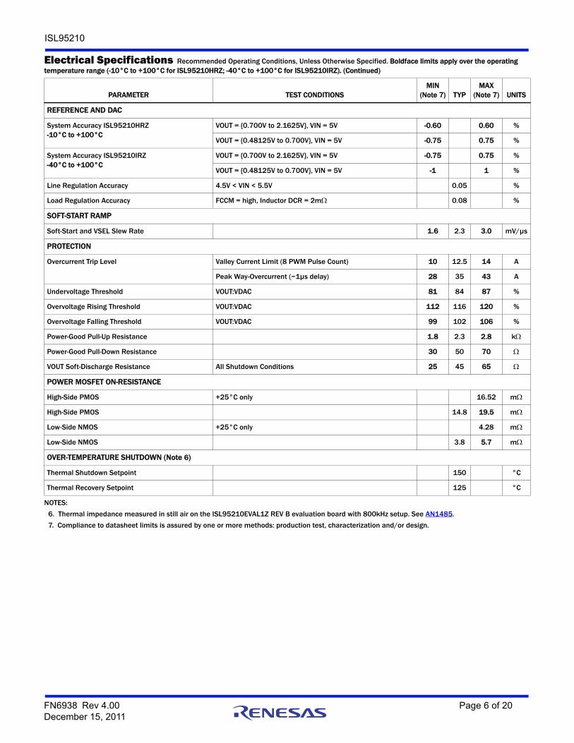
FIGURE 2. EFFICIENCY OF CIRCUIT SHOWN IN FIGURE 1 (INCLUDES INDUCTOR LOSSES)
VIN
PVCC
ENPG_IN
VSEL1FSET
MPCTMSELVSEL0FCCM T-PAD
VOUTVCC
AGND
PGND
PGOOD
PHASEVOUT = 1.2V
VIN = 5V
LOUT
420nH
COUT220µF
1µF
10µFCIN
CONTROLSIGNALS
POWER GOOD
VCC
+
ISL95210
LOUT
COUT
= MPC0740LR42C (NEC/TOKIN)
= 2TPLF220M5 (SANYO)
FSW= 800kHz
100
95
90
85
80
75
70
65
60
55
500 1 2 3 4 5 6 7 8 9 10
IOUT (A)
EF
FIC
IEN
CY
(%
)
VIN = 5VVOUT = 1.2VFSW = 800kHz
FN6938 Rev 4.00 Page 1 of 20December 15, 2011

FN
693
8R
ev 4
.00
Pag
e 2 of 20
De
cem
be
r 15
, 20
11
ISL9
521
0
PGOOD
MONITOR
E
L
E
ON
PG_IN
PGOOD
PGND
PHASE
VIN
PVCC
Functional Block Diagram
DAC AND
MARGIN LOGIC
SOFT-START
POR
BANDGAP
R4™ MODULATOR
FREQUENCY
CONTROL
DEAD-TIM
CONTRO
& ADAPTIV
SHOOT-
THROUGH
PROTECTIUNDERVOLTAGE
OVERVOLTAGE
PROTECTION
VOUT
FSET
THERMAL MONITOR
& PROTECTION
OVERCURRENT
PROTECTION
VSEL0
VSEL1
MSEL
MPCT
VCC
EN
FCCM
AGND PVCCVCC
10Ω

ISL95210
Pin ConfigurationISL95210
(32 LD QFN)TOP VIEW
1 2 3 4 5 6 7 8 9 10
27
26 25 24 23 22 21 20 19 18
16
15
14
13
12
11
28
29
30
31
32
17
MSEL
MPCT
VCC
VOUT
AGND
VSEL0
VS
EL
1
PG
OO
D
PG
_IN
PG
ND
PG
ND
PG
ND
PG
ND
PG
ND
VIN
VIN
DNC
PGND
PGND
PVCC
PVCC
VIN
FC
CM
FS
ET
EN
PH
AS
E
PH
AS
E
PH
AS
E
PH
AS
E
PH
AS
E
PH
AS
E
PH
AS
E
T-PAD (PGND)
Functional Pin DescriptionsPIN NAME FUNCTION
T-PAD(Thermal Pad)
PGND Power ground. This thermal pad provides a return path for power stage and switching currents, as well as a thermal path for removing heat from the IC into the board. Place thermal vias in the pad to the PGND plane.
1 FCCM Logic input for operating mode selection. Connect this pin to VCC for CCM regulation only. Connect this pin to AGND to allow discontinuous conduction mode for light-load efficiency. Float this pin for audio mode light-load switching.
2 FSET Tri-state digital input for programming the regulator switching frequency. Pull this pin to VCC for 800kHz switching. Pull this pin to GND for 400kHz switching. Leave this pin floating for 533kHz switching.
3 EN Logic input for enabling and disabling output voltage regulation. Pull this pin to VCC to begin regulation. Pull this pin to AGND to disable regulation.
4, 5, 6, 7, 8, 9, 10
PHASE Power stage switching node for output voltage regulation. Connect to the output inductor. All PHASE pins must be electrically connected together on the printed circuit board.
11 DNC Do not connect. This pin must be left floating under all conditions.
12, 13, 19, 20, 21, 22, 23
PGND Power ground. This pin provides a return path for power stage and switching currents. All PGND pins must be electrically connected together on the printed circuit board.
14, 15 PVCC Power input for the integrated MOSFET gate drivers. Connect to a 5V (±10%) supply. Both PVCC pins must be shorted on the printed circuit board. VIN and PVCC may be tied together (see Figure 1) when operating from a nominal 5V supply. However, PVCC requires a 5V (±10%) supply irrespective of VIN. It is connected to VCC through an integrated 10 resistor and therefore doubles as the power supply for IC bias. If VIN is below 4.5V, PVCC must receive a separate power supply input and decoupling capacitor (1µF typical).
16, 17, 18 VIN Power input for buck regulation stage. Bypass to PGND with one 10µF or 22µF ceramic capacitor. Connect to a 2.97V to 5.5V supply. All VIN pins must be electrically connected together on the printed circuit board.
24 PG_IN Input voltage for the power-good CMOS output. Connect this pin to the desired PGOOD output high level.
25 PGOOD Active CMOS output for power-good indication. High state is indicated when the output voltage is in regulation, and output is logic low otherwise. Logic high level is set by the voltage on the PG_IN pin.
26 VSEL1 DAC logic MSB input. Used to program preset output voltages of 0.60V, 0.75V, 0.90V, 1.00V, 1.05V, 1.10V, 1.20V, 1.50V, and 1.80V.
27 VSEL0 DAC logic LSB input. Used to program preset output voltages of 0.60V, 0.75V, 0.90V, 1.00V, 1.05V, 1.10V, 1.20V, 1.50V, and 1.80V.
FN6938 Rev 4.00 Page 3 of 20December 15, 2011

ISL95210
28 AGND Ground reference for analog signals. Connect this pin to the ground plane.
29 VOUT Sense point for output voltage regulation and output soft-discharge. Connect to the desired regulation point. A resistor divider can be used to program VOUT away from preset DAC and MARGIN values. However, the divider must not set VOUT more than 5% from the programmed value. See “Output Voltage Programming” on page 11 and Figure 34 for more information on this implementation.
30 VCC Power supply input used for regulator bias and precision references. Place a high frequency ceramic capacitor (0.1µF to 1µF) to AGND. PVCC provides power to VCC through an integrated 10 resistor.
31 MPCT 3-state logic input for programming the amount of output voltage margining as controlled by the MSEL pin. Pull the pin to GND for ±15% margining, to VCC for ±20% margining, and float the pin for ±10% margining.
32 MSEL Digital input for control of output voltage margining. Pull this pin to VCC to margin the output voltage to the high value. Leave this pin floating to margin the output voltage low. Pull this pin to AGND to regulate the nominally programmed output voltage value. The margin amount is dictated by the MPCT pin.
Functional Pin Descriptions (Continued)
PIN NAME FUNCTION
Ordering InformationPART NUMBER(Notes 1, 2, 3)
PARTMARKING
TEMP RANGE(°C)
PACKAGE(Pb-free)
PKG.DWG. #
ISL95210HRZ 95210 HRZ -10 to +100 32 Ld 6x4 QFN L32.6x4B
ISL95210IRZ 95210 IRZ -40 to +100 32 Ld 6x4 QFN L32.6x4B
ISL95210EVAL1Z Evaluation Board
NOTES:
1. Add “-T*” suffix for tape and reel. Please refer to TB347 for details on reel specifications.
2. These Intersil Pb-free plastic packaged products employ special Pb-free material sets, molding compounds/die attach materials, and 100% matte tin plate plus anneal (e3 termination finish, which is RoHS compliant and compatible with both SnPb and Pb-free soldering operations). Intersil Pb-free products are MSL classified at Pb-free peak reflow temperatures that meet or exceed the Pb-free requirements of IPC/JEDEC J STD-020.
3. For Moisture Sensitivity Level (MSL), please see device information page for ISL95210. For more information on MSL please see techbrief TB363.
FN6938 Rev 4.00 Page 4 of 20December 15, 2011

ISL95210
Absolute Maximum Ratings Thermal InformationAll pins . . . . . . . . . . . . . . . . . . . . . . . . . . . . . . . . . . . . . . . . . . -0.3V to +6V (DC)PHASE . . . . . . . . . . . . . . . . . . . . . . . . . . . . . . . . . . . . . . . -2V to +10V (< 10ns)VIN . . . . . . . . . . . . . . . . . . . . . . . . . . . . . . . . . . . . . . . . . . -0.3V to 8V (< 10ns)
Recommended Operating ConditionsVCC Supply Voltage . . . . . . . . . . . . . . . . . . . . . . . . . . . . . . . . . . . . .+5V ±10%PVCC Supply Voltage . . . . . . . . . . . . . . . . . . . . . . . . . . . . . . . . . . . .+5V ±10%VIN Supply Voltage . . . . . . . . . . . . . . . . . . . . . . . . . . . . . . . . +2.97V to +5.5V Junction Temperature (ISL95210HRZ) . . . . . . . . . . . . . . .-10°C to +125°CJunction Temperature (ISL95210IRZ) . . . . . . . . . . . . . . . .-40°C to +125°C
Thermal Resistance (Typical) JA (°C/W) JC (°C/W)32 Ld QFN Package (Notes 4, 5) . . . . . . . . 40 4
Maximum Junction Temperature . . . . . . . . . . . . . . . . . . . . . . . . . . . .+150°CMaximum Storage Temperature Range . . . . . . . . . . . . . .-65°C to +150°CPb-Free Reflow Profile . . . . . . . . . . . . . . . . . . . . . . . . . . . . . . . see link below
http://www.intersil.com/pbfree/Pb-FreeReflow.asp
CAUTION: Do not operate at or near the maximum ratings listed for extended periods of time. Exposure to such conditions may adversely impact productreliability and result in failures not covered by warranty.
NOTES:
4. JA is measured in free air with the component mounted on a high effective thermal conductivity test board with “direct attach” features. See Tech Brief TB379.
5. For JC, the “case temp” location is the center of the exposed metal pad on the package underside.
Electrical Specifications Recommended Operating Conditions, Unless Otherwise Specified. Boldface limits apply over the operating temperature range (-10°C to +100°C for ISL95210HRZ; -40°C to +100°C for ISL95210IRZ).
PARAMETER TEST CONDITIONSMIN
(Note 7) TYPMAX
(Note 7) UNITS
BIAS SUPPLIES
Shutdown Supply Current [PVCC] EN = low, VIN = PVCC = high 0.4 10 µA
Switching Supply Current [PVCC] EN = high, VCC = high, FSET = GND(400kHz), FCCM = high 7.2 mA
EN = high, VCC = high, FSET = FLOAT (533kHz), FCCM = high 8.9 mA
EN = high, VCC = high, FSET = high (800kHz), FCCM = high 12.2 mA
Standby Supply Current [PVCC] EN = high, VCC = high, FCCM = low, IOUT = 0A 1.9 2.7 mA
VCC POR (Power-On Reset) Threshold VCC rising 4.25 4.50 V
VCC falling 4.00 4.25 V
PWM MODULATOR
Oscillator Frequency Accuracy, FSW (ISL95210HRZ) FSET = GND (400kHz)/FLOAT (533kHz)/VCC (800kHz),TA = +25°C
-5 5 %
FSET = GND (400kHz)/FLOAT (533kHz)/VCC (800kHz), -10°C to +100°C
-10 10 %
Oscillator Frequency Accuracy, FSW (ISL95210IRZ) FSET = GND (400kHz)/FLOAT (533kHz)/VCC (800kHz),-40°C to +100°C
-15 15 %
CONTROL THRESHOLDS
EN Rising Threshold 2.0 V
EN Falling Threshold 1.0 V
FCCM, MPCT, MSEL, FSET, VSEL_ Input Low Threshold
1.20 1.50 1.80 V
FCCM, MPCT, MSEL, FSET, VSEL_ Input Floating Voltage
Input impedance > 1M 1.85 2.00 2.15 V
FCCM, MPCT, MSEL, FSET, VSEL_ Input High Threshold
2.2 2.50 2.8 V
FN6938 Rev 4.00 Page 5 of 20December 15, 2011
ISL95210
REFERENCE AND DAC
System Accuracy ISL95210HRZ-10°C to +100°C
VOUT = {0.700V to 2.1625V}, VIN = 5V -0.60 0.60 %
VOUT = {0.48125V to 0.700V}, VIN = 5V -0.75 0.75 %
System Accuracy ISL95210IRZ-40°C to +100°C
VOUT = {0.700V to 2.1625V}, VIN = 5V -0.75 0.75 %
VOUT = {0.48125V to 0.700V}, VIN = 5V -1 1 %
Line Regulation Accuracy 4.5V < VIN < 5.5V 0.05 %
Load Regulation Accuracy FCCM = high, Inductor DCR = 2m 0.08 %
SOFT-START RAMP
Soft-Start and VSEL Slew Rate 1.6 2.3 3.0 mV/µs
PROTECTION
Overcurrent Trip Level Valley Current Limit (8 PWM Pulse Count) 10 12.5 14 A
Peak Way-Overcurrent (~1µs delay) 28 35 43 A
Undervoltage Threshold VOUT:VDAC 81 84 87 %
Overvoltage Rising Threshold VOUT:VDAC 112 116 120 %
Overvoltage Falling Threshold VOUT:VDAC 99 102 106 %
Power-Good Pull-Up Resistance 1.8 2.3 2.8 k
Power-Good Pull-Down Resistance 30 50 70
VOUT Soft-Discharge Resistance All Shutdown Conditions 25 45 65
POWER MOSFET ON-RESISTANCE
High-Side PMOS +25°C only 16.52 m
High-Side PMOS 14.8 19.5 m
Low-Side NMOS +25°C only 4.28 m
Low-Side NMOS 3.8 5.7 m
OVER-TEMPERATURE SHUTDOWN (Note 6)
Thermal Shutdown Setpoint 150 °C
Thermal Recovery Setpoint 125 °C
NOTES:
6. Thermal impedance measured in still air on the ISL95210EVAL1Z REV B evaluation board with 800kHz setup. See AN1485.
7. Compliance to datasheet limits is assured by one or more methods: production test, characterization and/or design.
Electrical Specifications Recommended Operating Conditions, Unless Otherwise Specified. Boldface limits apply over the operating temperature range (-10°C to +100°C for ISL95210HRZ; -40°C to +100°C for ISL95210IRZ). (Continued)
PARAMETER TEST CONDITIONSMIN
(Note 7) TYPMAX
(Note 7) UNITS
FN6938 Rev 4.00 Page 6 of 20December 15, 2011
ISL95210
Typical Performance Curves
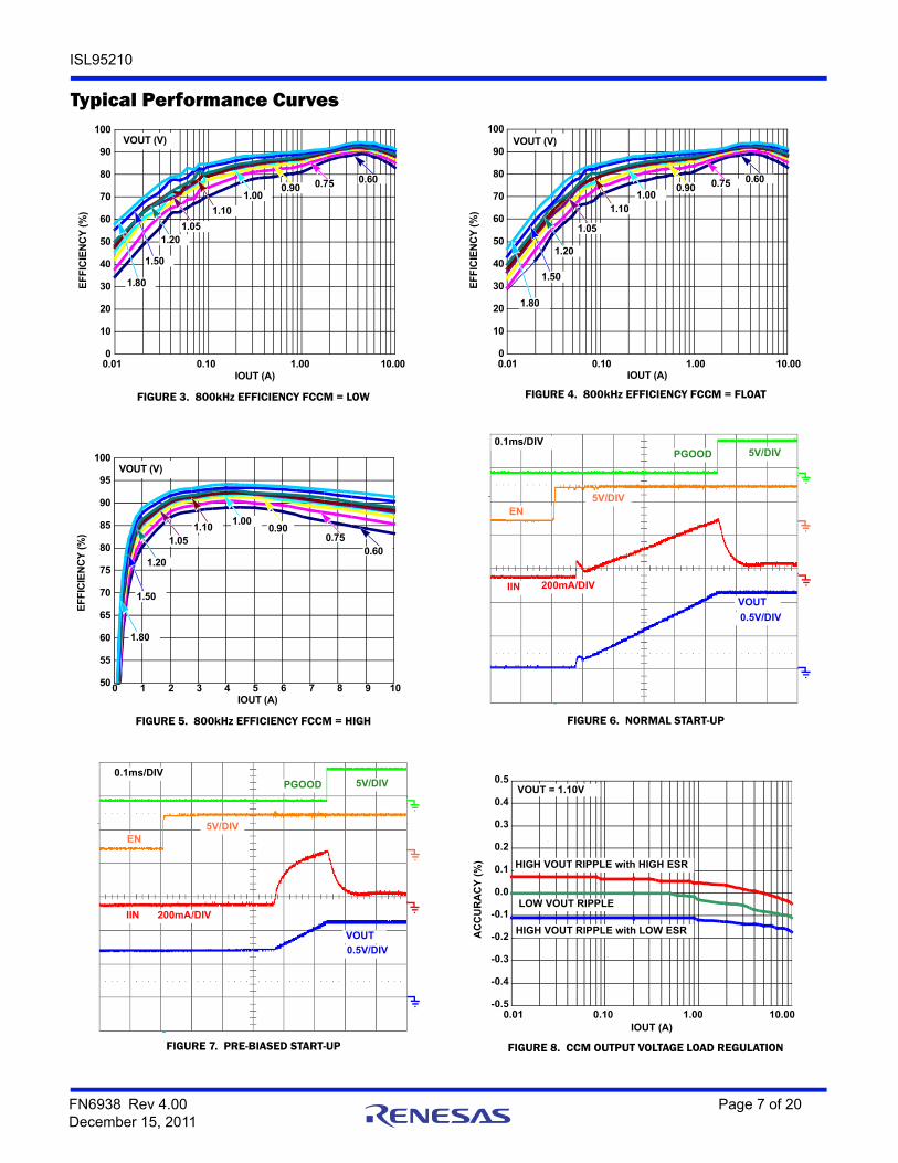
FIGURE 3. 800kHz EFFICIENCY FCCM = LOW FIGURE 4. 800kHz EFFICIENCY FCCM = FLOAT
FIGURE 5. 800kHz EFFICIENCY FCCM = HIGH FIGURE 6. NORMAL START-UP
FIGURE 7. PRE-BIASED START-UP FIGURE 8. CCM OUTPUT VOLTAGE LOAD REGULATION
0
10
20
30
40
50
60
70
80
90
100
0.01 0.10 1.00 10.00IOUT (A)
EF
FIC
IEN
CY
(%
)
0.600.750.901.00
1.05
1.10
1.20
1.50
1.80
VOUT (V)
0
10
20
30
40
50
60
70
80
90
100
0.01 0.10 1.00 10.00
EF
FIC
IEN
CY
(%
)
IOUT (A)
0.600.750.901.00
1.05
1.10
1.20
1.50
1.80
VOUT (V)
50
55
60
65
70
75
80
85
90
95
100
0 1 2 3 4 5 6 7 8 9 10
EF
FIC
IEN
CY
(%
)
IOUT (A)
0.600.75
0.901.00
1.051.10
1.20
1.50
1.80
VOUT (V)
PGOOD 5V/DIV
EN5V/DIV
IIN 200mA/DIV
VOUT
0.5V/DIV
0.1ms/DIV
PGOOD 5V/DIV
EN5V/DIV
IIN 200mA/DIV
VOUT
0.5V/DIV
0.1ms/DIV
-0.5
-0.4
-0.3
-0.2
-0.1
0.0
0.1
0.2
0.3
0.4
0.5
0.01 0.10 1.00 10.00
AC
CU
RA
CY
(%
)
IOUT (A)
VOUT = 1.10V
HIGH VOUT RIPPLE with HIGH ESR
HIGH VOUT RIPPLE with LOW ESR
LOW VOUT RIPPLE
FN6938 Rev 4.00 Page 7 of 20December 15, 2011
ISL95210
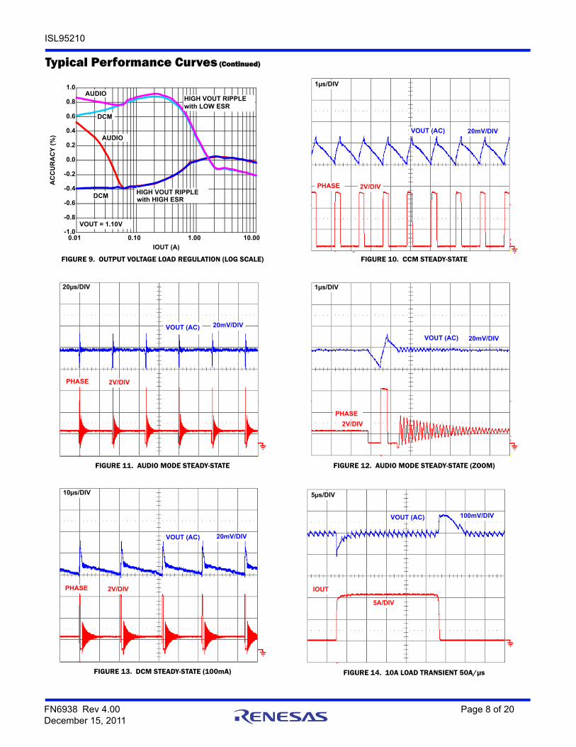
FIGURE 9. OUTPUT VOLTAGE LOAD REGULATION (LOG SCALE) FIGURE 10. CCM STEADY-STATE
FIGURE 11. AUDIO MODE STEADY-STATE FIGURE 12. AUDIO MODE STEADY-STATE (ZOOM)
FIGURE 13. DCM STEADY-STATE (100mA) FIGURE 14. 10A LOAD TRANSIENT 50A/µs
Typical Performance Curves (Continued)
-1.0
-0.8
-0.6
-0.4
-0.2
0.0
0.2
0.4
0.6
0.8
1.0
0.01 0.10 1.00 10.00
AC
CU
RA
CY
(%
)
IOUT (A)
VOUT = 1.10V
AUDIO
DCM
AUDIO
DCM
HIGH VOUT RIPPLEwith LOW ESR
HIGH VOUT RIPPLEwith HIGH ESR
PHASE 2V/DIV
VOUT (AC) 20mV/DIV
1µs/DIV
PHASE 2V/DIV
VOUT (AC) 20mV/DIV
20µs/DIV
PHASE
2V/DIV
VOUT (AC) 20mV/DIV
1µs/DIV
PHASE 2V/DIV
20mV/DIV
10µs/DIV
VOUT (AC)
IOUT
5A/DIV
100mV/DIV
5µs/DIV
VOUT (AC)
FN6938 Rev 4.00 Page 8 of 20December 15, 2011

ISL95210
FIGURE 15. 10A LOAD TRANSIENT 50A/µs (ZOOM RISING EDGE) FIGURE 16. 10A LOAD TRANSIENT 50A/µs (ZOOM FALLING EDGE)
FIGURE 17. 10A LOAD TRANSIENT 5A/µs FIGURE 18. VSEL1 TRANSITIONS 0.90V TO 1.80V
FIGURE 19. NORMAL SHUT-DOWN FIGURE 20. OVERVOLTAGE SHUT-DOWN (VDAC = 1.00V)
Typical Performance Curves (Continued)
IOUT
5A/DIV
50mV/DIV
PHASE 5V/DIV
1µs/DIV
VOUT (AC)
IOUT
5A/DIV
50mV/DIV
PHASE 5V/DIV
2µs/DIV
VOUT (AC)
IOUT
5A/DIV
100mV/DIVVOUT (AC)
5µs/DIV 0.2ms/DIV
VSEL1
2V/DIV
VOUT
500mV/DIV
PGOOD 5V/DIV
EN 5V/DIV
VOUT
0.5V/DIV5ms/DIV
PGOOD 5V/DIV
VOUT200mV/DIV
10µs/DIV
PHASE 2V/DIV
FN6938 Rev 4.00 Page 9 of 20December 15, 2011

ISL95210
FIGURE 21. UNDERVOLTAGE SHUT-DOWN (VDAC = 1.00V) FIGURE 22. OVERCURRENT SHUTDOWN
FIGURE 23. CURRENT DERATING OVER-TEMPERATURE FIGURE 24. CURRENT DERATING OVER-TEMPERATURE (ZOOM)
NOTE: Figures 23 and 24 were generated on the ISL95210EVAL1Z REV B evaluation board (4-layers/2oz. copper). The test conditions were 5VIN and 1.8VOUT. The junction temperature was characterized by measuring the shift over-temperature of an integrated polysilicon resistor. All other above figures were generated with the typical application schematic found in Figure 1, unless otherwise specified. For more details on the layer stack up of the evaluation board, please see the ISL95210 Application Note (AN1485).
Typical Performance Curves (Continued)
PGOOD 5V/DIV
VOUT200mV/DIV
10µs/div
PHASE 2V/DIV
PHASE5V/DIV
PGOOD
5V/DIV
IL
5A/DIV
0
2
4
6
8
10
12
25 50 75 100 125
AMBIENT TEMPERATURE (°C)
MA
XIM
UM
CO
NT
INU
OU
S
85
OU
TP
UT
CU
RR
EN
T (
A)
200 LFM
100 LFM
300 LFM
AIR FLOW
0 LFM
0
2
4
6
8
10
12
85 90 95 100 105 110 115 120 125
AMBIENT TEMPERATURE (°C)
MA
XIM
UM
CO
NT
INU
OU
S O
UT
PU
T C
UR
RE
NT
(A
) 200 LFM
100 LFM
300 LFM
AIR FLOW
0 LFM
FN6938 Rev 4.00 Page 10 of 20December 15, 2011

ISL95210
Theory of OperationThe following sections will provide a detailed description of the inner workings of the ISL95210 10A integrated FET regulator.
Start -UpThe ISL95210 will not respond to any logic inputs until VCC and PVCC are above the power-on reset (POR) level as described in the “Electrical Specifications” table on page 5. Once the POR condition is achieved, the ISL95210 will then acknowledge the states of its logic inputs. If the EN pin is pulled above the rising threshold, the regulator is commanded on and the soft-start sequence is initiated.
During soft-start, the programmed output voltage set point is determined by the logic states of VSEL0, VSEL1, MPCT and MSEL. The output then ramps digitally to the regulation voltage in 2.5mV/µs steps. Once the output voltage achieves regulation, the power-good monitor output (PGOOD) is toggled high to the voltage provided on the PG_IN pin. Figure 25 illustrates the ideal soft-start behavior.
Using the values in Tables 1 and 2, the soft-start interval can be easily calculated by Equation 1.
The units of Equation 1 are in microseconds. For example:
- VDAC = 1.200V
- tSS = 1.200V / 0.0025 = 480µs
The fixed soft-start slew rate of 2.5mV/µs allows for easy calculation of the in-rush current.
Consequently, the in-rush is manageable for all practical values of output capacitance. For example:
- COUT = 330µF
- Inrush Current = 2500*330µF = 0.825A
Output Voltage ProgrammingThe highly integrated nature of the ISL95210 simplifies design and reduces component count. The VSEL0 and VSEL1 pins are 3-state logic inputs to an integrated DAC that controls the output voltage set point as prescribed in Table 1.
This allows the user to program the output voltage without the use of a resistor divider network. However, if the user wishes to program values of VOUT away from the DAC values, a resistor divider can be used. However, because the input impedance of the VOUT pin is relatively low, the top resistor in the divider stack (R1 in Figure 31) must be kept small to minimize regulation error as the internal resistance changes over-temperature and process tolerances. A 100 resistor is recommended. The bottom resistor in the divider stack (R2 in Figure 31) can be derived from Equation 3:
For example:
- Desired VOUT = 1.35V
- VDAC = 1.32V (1.2V +10% margin)
- R1 = 100
- R2 = 4.351k(select nearest standard value)
NOTE: The resistor divider should not be used to program VOUT more than 5% away from any preset DAC value. If this limit is exceeded, the modulator will be severely imbalanced and may result in loop instability and regulator shutdown.
The use of a resistor network also limits the soft discharge feature of the ISL95210. More detail on this operation can be found in the “Soft-Discharge” on page 15.
In addition to digitally controlled output voltage programming, the ISL95210 includes the ability to margin the output voltage up and down from the set point for use in end-of-line manufacturing reliability tests. The MPCT pin controls the amount of margining desired by the user and the MSEL pin determines when margining is engaged. In all margining conditions, the output voltage is slewed to the new value at the soft-start rate of
FIGURE 25. IDEALIZED SOFT-START WAVEFORM
PG_OUT
EN
VOUT
1us
2.5mV
DAC Voltage
tSS
EN
DAC VOLTAGE
VOUT 2.5mV
1µs tSS
PGOOD
tSS
VDAC0.0025------------------= (EQ. 1)
IINRUSH 2500 COUT = (EQ. 2)
TABLE 1. DAC CONTROLLED OUTPUT VOLTAGE SETTINGS
VSEL1 VSEL0 VOUT (V)
0 0 0.600
0 FLOAT 0.750
0 1 0.900
FLOAT 0 1.000
FLOAT FLOAT 1.050
FLOAT 1 1.100
1 0 1.200
1 FLOAT 1.500
1 1 1.800
NOTE: 1 = Input High, 0 = Input Low, FLOAT = Input unconnected or high-Z (see “Electrical Specifications” table for details).
R2R1 VDAC
VOUT2 R1205k--------------- 205k R1+
205k--------------------------- –+ VDAC
-------------------------------------------------------------------------------------------------------= (EQ. 3)
FN6938 Rev 4.00 Page 11 of 20December 15, 2011

ISL95210
2.5mV/µs. Table 2 shows the output voltage as dictated by MPCT and MSEL.
Each of the margin targets represents the DAC code nearest to the desired value. Table 3 shows the actual targets for each margin setting (see Table 4 on page 17 for the full output truth table).
Both the DAC and margining features can be used “on the fly”, meaning the voltage can be changed during normal operation.
Regulation
R4™ MODULATORThe R4 modulator is an advanced current-mode hysteretic control scheme that generates a synthetic current signal on chip instead of measuring real current. This has the benefit of producing a cleaner and lower jitter system versus conventional current-mode hysteretic architectures.
R4™ also employs a highly balanced architecture that greatly reduces the need for high DC loop gain traditionally required for output voltage regulation accuracy. This allows the R4™ modulator to accurately regulate without the need for an integrator in the feedback loop. Another benefit of the balanced system is that it does not require compensation for stability over a wide range of designs. The result is a power solution that is
flexible and easy to design with minimal components. A complete point of load regulator can be designed with the ISL95210 using only 4 external components.
Figure 26 shows the basic error-amplifier configuration for the R4™ controller. A hysteretic comparator monitors the synthetic current signal against the error voltage and corresponding window voltage to determine the PWM switching events.
STABILITYThe R4™ balanced architecture creates a control loop that does not require compensation for an extremely wide range of output filters (LOUT, COUT). However, there are corners of operation that will destabilize the loop and result in oscillatory behavior in VOUT.
The filters that push the control loop toward instability are ones that add a considerable amount of phase delay to the output voltage. In general, phase delay increases as output capacitance decreases in conjunction with reduced output capacitor equivalent series resistance (ESR). For this reason, output filters that are all-ceramic based have the most difficulty achieving stable regulation.
The first indication that the ISL95210 is nearing instability is when its step load response begins to have ring-back. Ring-back occurs when the PWM on pulse in response to a sharp increase in output load is so long as to cause the output voltage to overshoot the regulation point before fully recovering. Equation 4 approximates the boundary condition between normal recovery and ring-back as a function of operating parameters
where:
- COUT = Total output capacitance in Farads
- LOUT = Output inductance in Henries
- D = Steady-state duty cycle (VOUT / VIN)
- ESR = Output capacitor equivalent series resistance
- ISTEP = Expected load step (worst case is preferred)
- IL = Inductor ripple current
- FSW = Switching frequency
- K = Modulator factor:
- 3700 for 400kHz FSW
- 4933 for 533kHz FSW
- 7400 for 800kHz FSW
As good design practices dictate, a system should be designed safely away from this boundary to cover any tolerance shifts that may occur. For example, if the output capacitor in Figure 1 is replaced with low-ESR ceramics and reduced until the inequality
TABLE 2. OUTPUT VOLTAGE MARGINING CONTROL
MSEL MPCT RESULT
0 0 NO MARGINING
0 FLOAT NO MARGINING
0 1 NO MARGINING
FLOAT 0 MARGIN DOWN DAC - 15%
FLOAT FLOAT MARGIN DOWN DAC - 10%
FLOAT 1 MARGIN DOWN DAC - 20%
1 0 MARGIN UP DAC + 15%
1 FLOAT MARGIN UP DAC + 10%
1 1 MARGIN UP DAC + 20%
NOTE: 1 = Input High, 0 = Input Low, FLOAT = Input unconnected or high-Z (see “Electrical Specifications” table for details).
TABLE 3. OUTPUT VOLTAGE MARGIN TARGETS
VOUT -20% -15% -10% +10% +15% +20%
0.600 0.481 0.513 0.538 0.663 0.688 0.719
0.750 0.600 0.638 0.675 0.825 0.863 0.900
0.900 0.719 0.763 0.813 0.988 1.038 1.081
1.000 0.800 0.850 0.900 1.100 1.150 1.200
1.050 0.838 0.894 0.944 1.156 1.206 1.263
1.100 0.881 0.938 0.988 1.213 1.263 1.325
1.200 0.963 1.019 1.081 1.319 1.381 1.438
1.500 1.200 1.275 1.350 1.650 1.7250 1.800
1.800 1.438 1.531 1.619 1.981 2.069 2.163
FIGURE 26. BASIC R4™ PWM SIGNAL GENERATION
VOUT
VDAC
+VW
-
ERROR-AMPLIFIER
HYSTERETIC WINDOW VOLTAGE
COMP VOLTAGE
SYNTHETIC CURRENT
PWM
(EQ. 4)COUT ESR K LOUT COUT + ISTEPD D
FSW IL----------------------------
FN6938 Rev 4.00 Page 12 of 20December 15, 2011

ISL95210
in Equation 4 is not met, transient ring-back performance similar to what is shown in Figure 27 will occur.
In this example, the total output capacitance was 76µF with an ESR of approximately 1m. When the values are put into Equation 4, the inequality is not met:
x 3.12·10-7 > 3.25·10-7
If additional ceramics are added to increase COUT to 120µF with an ESR of approximately 0.67m, the ring-back condition is eliminated, providing the transient results seen in Figure 28.
When the new values are evaluated in Equation 4, the following results are observed:
4.53·10-7 > 3.25·10-7
This result shows a clean, stable solution when the inequality is satisfied. It should be noted that when the capacitance in this example is decremented between 120µF and 76µF, the severity and frequency of ring-back increases. It can occur prior to violating Equation 4. This is due to the non-idealities that exist in real systems and some simplifications in the derivation process. Care should be taken to design away from the boundary condition. The above example became fully stable (zero ring-back) when the inequality’s percentage difference was ~35%.
TRANSIENT RESPONSEAs with all current-mode hysteretic style controllers, the ISL95210 will increase and decrease switching frequency in response to load transient events. This oversampling quickens the converters response and minimizes output voltage deviation. The change in frequency is achieved by the movement on the COMP voltage seen in Figure 26. When the load current changes up or down, there is an proportional movement on COMP. The movement on COMP naturally changes the hysteretic window size for both PWM edges. Upward swings in COMP (due to increasing load current) make the effective hysteretic window larger during PWM on times and smaller during PWM off times. The result is increased switching frequency.
Conversely, downward swings in COMP (due to decreasing load current) make the effective hysteretic window smaller during PWM on times and larger during PWM off times. Switching frequency is reduced in this scenario. Figure 29 illustrates the idealized effect on switching frequency from movements in COMP in response to load transient events.
Unlike more traditional current-mode hysteretic architectures, R4™ does not require an error-integrating capacitor in the feedback loop. This removes significant delay in the control loop and produces extremely fast transient response to changes in load current.
The speed of response allows system designers to use less output capacitance and save on board area and cost.
Figure 30 depicts a comparison of the R4™ modulator vs. various classic architectures in response to a load step-up transient. The
FIGURE 27. ISL95210 LOAD TRANSIENT RESPONSE WITH RING-BACK CONDITIONS FROM EXCESSIVE VOUT PHASE DELAY
FIGURE 28. ISL95210 LOAD TRANSIENT RESPONSE WITHOUT RING-BACK CONDITIONS
20mV/DIV
2µs/DIV
VOUT (AC)
VIN = 5VVOUT = 1.2VISTEP = 0-6AFSW = 800kHz
20mV/DIV
2µs/DIV
VOUT (AC)
VIN = 5VVOUT = 1.2VISTEP = 0-6AFSW = 800kHz
FIGURE 29. IDEALIZED EFFECT OF LOAD TRANSIENTS ON SWITCHING FREQUENCY
IOUT
SYNTHETIC CURRENT
HYSTERETIC WINDOW VOLTAGE
COMP VOLTAGE
PWM
VOUT
BOTH PWM EDGES ARE MODULATED DURING LOAD TRANSIENT
FN6938 Rev 4.00 Page 13 of 20December 15, 2011

ISL95210
dotted red and blue lines represent the time delayed behavior of VOUT and VCOMP when an integrator is used. The solid red and blue lines illustrate the increased response of R4™ in the absence of the integrating capacitor.
DISCONTINUOUS CONDUCTION MODESThe ISL95210 supports two power saving modes of operation during light load conditions. If FCCM is asserted high, the regulator remains in continuous conduction mode (CCM) which offers the best transient response and the most stable operating frequency.
If the FCCM pin is pulled to ground potential, the regulator is allowed to operate in full discontinuous conduction mode (DCM) when the load becomes sufficiently low. In this mode, the inductor current is monitored and prohibited from going negative. When the inductor current reaches zero, both internal power MOSFETs are turned off. The output voltage then decays solely as a function of load. The power FETs remain off until the output voltage droops enough to trigger a PWM on pulse. Because the rate of decay of VOUT scales proportionally with load, so does the switching frequency. This increases efficiency as the relatively fixed power loss associated with switching the power FETs is averaged over the switching period.
If the FCCM pin is left floating, the ISL95210 will operate in audio mode DCM. This mode operates largely the same as full DCM mode with one exception; the switching period is monitored cycle by cycle. If the load diminishes to a point where the switching frequency begins to drop below ~28kHz, the ISL95210 control loop will issue a PWM on pulse to ensure the frequency remains above the upper threshold for human hearing. This allows flexibility for designs that are sensitive to audio frequency interference.
The R4™ architecture seamlessly enters and exits all power saving modes to ensure accurate regulation.
Protection and Shutdown FeaturesThe ISL95210 offers a full suite of protection features to reduce the risk of damage to the IC and load. They include under and overvoltage monitoring and protection as well as protection against excessive current and thermal operating conditions.
UNDERVOLTAGE PROTECTIONIf the output voltage dips too low during normal operation, the ISL95210 recognizes a fault condition and shuts down. When VOUT goes 16% below VDAC, the power-good monitor flags PGOOD low and tri-states the PHASE node by turning off both integrated power MOSFETs. In addition, the soft-discharge MOSFET is turned on to gently pull the output voltage to ground potential for the next restart.
The undervoltage fault remains latched until a POR event or EN is toggled.
OVERVOLTAGE PROTECTIONDuring normal operation, the output voltage is monitored at all times to ensure it does not exceed the set point by more than 16%. Excessively high voltages can cause failure to output capacitors as well as the load. If VOUT goes above 116% of DAC, the power-good monitor is flagged by toggling PGOOD low and the IC enters overvoltage protection mode.
In overvoltage protection mode, the upper P-Channel MOSFET is latched off until the fault is cleared. In addition, VOUT is compared against the reference DAC voltage. If VOUT is above DAC, the lower N-channel MOSFET is turned on to pull VOUT down. If VOUT falls below DAC, the lower N-Channel MOSFET is turned off. This process repeats until the fault condition is cleared through VCC/PVCC POR or a recycling of the EN pin. This produces a soft-crowbar action that can effectively pull the output away from dangerously high voltage levels without causing the negative voltage swings on VOUT that are present with full crowbar implementations of overvoltage protection.
OVERCURRENT PROTECTIONIf the current draw from the load becomes too high during operation, the IC protects itself and the load by latching off. The overcurrent mechanism is implemented as a two-fold protection scheme.
The ISL95210 continuously monitors the lower N-channel MOSFET current. It stores the valley of the inductor current each cycle and compares it against the lower overcurrent protection (OCP) threshold of 11A nominally. If the OCP threshold is achieved for 8 consecutive PWM cycles, an overcurrent fault is detected and the IC is shutdown. In this event, power-good monitor flags PGOOD low and tri-states both switching power MOSFETs and turns on the soft-discharge FET. Inductor valley current is used to ensure that the minimum OCP threshold is above the maximum ISL95210’s normal maximum load of 10A regardless of chosen inductor value.
In addition to valley current limit, the upper P-Channel MOSFET current is continuously monitored. If a catastrophic overcurrent event is encountered (e.g. short circuit on VOUT), the ISL95210 immediately responds to protect the output by latching both MOSFETs off and engaging the soft-discharge FET. The power-good monitor flags PGOOD low and the IC remains latched off until POR or EN is toggled.
THERMAL PROTECTIONThe ISL95210 actively monitors the die temperature to protect against harmful thermal operating conditions. If the silicon temperature exceeds +150°C, the controller will suspend
FIGURE 30. CLASSIC ARCHITECTURES vs R4™ IDEALIZED TRANSIENT RESPONSE
CLASSIC VOLTAGE-MODE OR
t
R4™
VOUT
VCOMP
IOUT
CURRENT-MODE ARCHITECTURE
FN6938 Rev 4.00 Page 14 of 20December 15, 2011
ISL95210
operation and shut down until the IC junction temperature falls below +135°C. Once the temperature has fallen below the lower protection threshold, the IC will resume normal operation following a POR event or toggling of the EN input.
POWER-GOOD MONITORA status indicator is provided to inform the system whether or not the ISL95210 output voltage is in regulation or if a fault has occurred. If VCC and PVCC are above the POR threshold, the part is enabled, and no faults have been detected, PGOOD will toggle high.
The power-good monitor is a CMOS configuration (refer to the “Functional Block Diagram” on page 2). This allows the user to provide any voltage to indicate when power is good. The voltage provided on to the PG_IN pin will be used as the logic high value for PGOOD. This has the advantage over open-drain configurations of saving a pull-up resistor. A pull-up resistor on PGOOD can still be used if desired. In this configuration, the PG_IN pin needs to be floated.
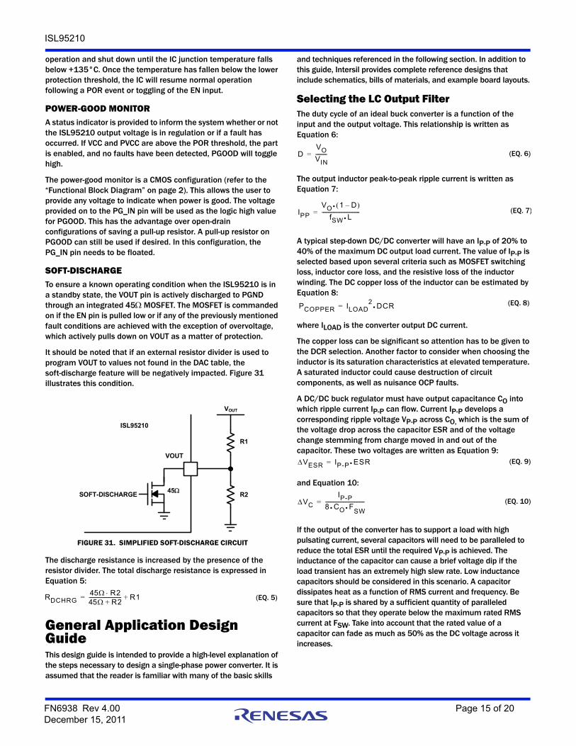
SOFT-DISCHARGETo ensure a known operating condition when the ISL95210 is in a standby state, the VOUT pin is actively discharged to PGND through an integrated 45 MOSFET. The MOSFET is commanded on if the EN pin is pulled low or if any of the previously mentioned fault conditions are achieved with the exception of overvoltage, which actively pulls down on VOUT as a matter of protection.
It should be noted that if an external resistor divider is used to program VOUT to values not found in the DAC table, the soft-discharge feature will be negatively impacted. Figure 31 illustrates this condition.
The discharge resistance is increased by the presence of the resistor divider. The total discharge resistance is expressed in Equation 5:
General Application Design GuideThis design guide is intended to provide a high-level explanation of the steps necessary to design a single-phase power converter. It is assumed that the reader is familiar with many of the basic skills
and techniques referenced in the following section. In addition to this guide, Intersil provides complete reference designs that include schematics, bills of materials, and example board layouts.
Selecting the LC Output FilterThe duty cycle of an ideal buck converter is a function of the input and the output voltage. This relationship is written as Equation 6:
The output inductor peak-to-peak ripple current is written as Equation 7:
A typical step-down DC/DC converter will have an IP-P of 20% to 40% of the maximum DC output load current. The value of IP-P is selected based upon several criteria such as MOSFET switching loss, inductor core loss, and the resistive loss of the inductor winding. The DC copper loss of the inductor can be estimated by Equation 8:
where ILOAD is the converter output DC current.
The copper loss can be significant so attention has to be given to the DCR selection. Another factor to consider when choosing the inductor is its saturation characteristics at elevated temperature. A saturated inductor could cause destruction of circuit components, as well as nuisance OCP faults.
A DC/DC buck regulator must have output capacitance CO into which ripple current IP-P can flow. Current IP-P develops a corresponding ripple voltage VP-P across CO, which is the sum of the voltage drop across the capacitor ESR and of the voltage change stemming from charge moved in and out of the capacitor. These two voltages are written as Equation 9:
and Equation 10:
If the output of the converter has to support a load with high pulsating current, several capacitors will need to be paralleled to reduce the total ESR until the required VP-P is achieved. The inductance of the capacitor can cause a brief voltage dip if the load transient has an extremely high slew rate. Low inductance capacitors should be considered in this scenario. A capacitor dissipates heat as a function of RMS current and frequency. Be sure that IP-P is shared by a sufficient quantity of paralleled capacitors so that they operate below the maximum rated RMS current at FSW. Take into account that the rated value of a capacitor can fade as much as 50% as the DC voltage across it increases.
FIGURE 31. SIMPLIFIED SOFT-DISCHARGE CIRCUIT
VOUT
SOFT-DISCHARGE
VOUT
R1
R2
ISL95210
45
RDCHRG45 R245 R2+-------------------------- R1+= (EQ. 5)
DVOVIN---------= (EQ. 6)
(EQ. 7)IPP
VO 1 D–
fSW L------------------------------=
(EQ. 8)PCOPPER ILOAD2
DCR=
VESR IP-P E SR= (EQ. 9)
VC
IP-P8 CO F
SW
-------------------------------= (EQ. 10)
FN6938 Rev 4.00 Page 15 of 20December 15, 2011
ISL95210
Selection of the Input CapacitorThe important parameters for the bulk input capacitance are the voltage rating and the RMS current rating. For reliable operation, select bulk capacitors with voltage and current ratings above the maximum input voltage and capable of supplying the RMS current required by the switching circuit. Their voltage rating should be at least 1.25x greater than the maximum input voltage, while a voltage rating of 1.5x is a preferred rating. Figure 32 is a graph of the input RMS ripple current, normalized relative to output load current, as a function of duty cycle and is adjusted for a converter efficiency of 80%. The ripple current calculation is written as Equation 11:
where:
- x is a multiplier (0 to 1) corresponding to the inductor peak-to-peak ripple amplitude expressed as a percentage of IMAX (0% to 100%)
- D is the duty cycle that is adjusted to take into account the efficiency of the converter, which is written as Equation 12:
In addition to the bulk capacitance, some low ESL ceramic capacitance is recommended to decouple between the drain of the high-side MOSFET and the source of the low-side MOSFET.
Typical Applications CircuitsThere are two main variants to typical application schematic shown in Figure 1. The first of these is when an input voltage lower than 5V is desired. This requires the designer to provide separate power supplies to VIN and PVCC as the ISL95210 requires a 5V bias to operate properly. Figure 33 illustrates this configuration for a VIN of 3.3V.
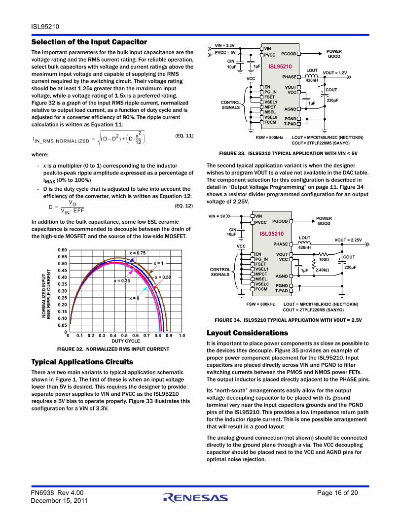
The second typical application variant is when the designer wishes to program VOUT to a value not available in the DAC table. The component selection for this configuration is described in detail in “Output Voltage Programming” on page 11. Figure 34 shows a resistor divider programmed configuration for an output voltage of 2.25V.
Layout ConsiderationsIt is important to place power components as close as possible to the devices they decouple. Figure 35 provides an example of proper power component placement for the ISL95210. Input capacitors are placed directly across VIN and PGND to filter switching currents between the PMOS and NMOS power FETs. The output inductor is placed directly adjacent to the PHASE pins.
Its “north-south” arrangements easily allow for the output voltage decoupling capacitor to be placed with its ground terminal very near the input capacitors grounds and the PGND pins of the ISL95210. This provides a low impedance return path for the inductor ripple current. This is one possible arrangement that will result in a good layout.
The analog ground connection (not shown) should be connected directly to the ground plane through a via. The VCC decoupling capacitor should be placed next to the VCC and AGND pins for optimal noise rejection.
FIGURE 32. NORMALIZED RMS INPUT CURRENT
(EQ. 11)IIN_RMS NORMALIZED D D
2– D
x2
12------
+=
DVO
VIN EFF--------------------------= (EQ. 12)
0 0.1 0.2 0.3 0.4 0.5 0.6 0.7 0.8 0.9 1.00
0.05
0.10
0.15
0.20
0.25
0.30
0.35
0.40
0.45
0.50
0.55
0.60
NO
RM
AL
IZE
D IN
PU
T
DUTY CYCLE
RM
S R
IPP
LE
CU
RR
EN
T
x = 1
x = 0.75
x = 0.50x = 0.25
x = 0
FIGURE 33. ISL95210 TYPICAL APPLICATION WITH VIN < 5V
FIGURE 34. ISL95210 TYPICAL APPLICATION WITH VOUT = 2.5V
VIN
PVCC
ENPG_IN
VSEL1FSET
MPCTMSELVSEL0FCCM T-PAD
VOUTVCC
AGND
PGND
PGOOD
PHASEVOUT = 1.2V
VIN = 3.3V
LOUT
420nH
COUT
220µF1µF
10µFCIN
CONTROLSIGNALS
POWER GOOD
VCC
+
ISL95210
LOUTCOUT
= MPC0740LR42C (NEC/TOKIN)= 2TPLF220M5 (SANYO)
1µF
FSW = 800kHz
PVCC = 5V
VIN
PVCC
ENPG_IN
VSEL1FSET
MPCTMSELVSEL0FCCM T-PAD
VOUTVCC
AGND
PGND
PGOOD
PHASEVOUT = 2.25V
VIN = 5V
LOUT
420nH
COUT
220µF1µF
10µFCIN
CONTROLSIGNALS
POWER GOOD
VCC
+
ISL95210
LOUTCOUT
= MPC0740LR42C (NEC/TOKIN)= 2TPLF220M5 (SANYO)
100
2.49k
FSW = 800kHz
FN6938 Rev 4.00 Page 16 of 20December 15, 2011

ISL95210
The colored shapes represent the following power planes:
Copper Size for the Phase NodeThe parasitic capacitance and parasitic inductance of the phase node should be kept very low to minimize ringing. It is best to limit the size of the PHASE node copper in strict accordance with the current and thermal management of the application. An MLCC should be connected directly between VIN and PGND to suppress the turn-off voltage spike. This is achieved by placing the MLCC as close to the IC as possible and adjacent to VIN and PGND.
Full Output Voltage Truth Table
PGND PHASE
VIN VOUT
FIGURE 35. ISL95210 POWER COMPONENT LAYOUT EXAMPLE
LOUT(7x7mm)
COUT(D-case)
CIN(1206)
ISL95210(4x6mm)
TABLE 4. OUTPUT VOLTAGE TRUTH TABLE
MSEL MPCT VSEL1 VSEL0 VOUT
FLOAT 1 0 0 0.48125
FLOAT 0 0 0 0.51250
FLOAT FLOAT 0 0 0.53750
0 0 0 0 0.60000
0 FLOAT 0 0 0.60000
0 1 0 0 0.60000
FLOAT 1 0 FLOAT 0.60000
FLOAT 0 0 FLOAT 0.63750
1 FLOAT 0 0 0.66250
FLOAT FLOAT 0 FLOAT 0.67500
1 0 0 0 0.68750
FLOAT 1 0 1 0.71875
1 1 0 0 0.71875
0 0 0 FLOAT 0.75000
0 FLOAT 0 FLOAT 0.75000
0 1 0 FLOAT 0.75000
FLOAT 0 0 1 0.76250
FLOAT 1 FLOAT 0 0.80000
FLOAT FLOAT 0 1 0.81250
1 FLOAT 0 FLOAT 0.82500
FLOAT 1 FLOAT FLOAT 0.83750
FLOAT 0 FLOAT 0 0.85000
1 0 0 FLOAT 0.86250
FLOAT 1 FLOAT 1 0.88125
FLOAT 0 FLOAT FLOAT 0.89375
0 0 0 1 0.90000
0 FLOAT 0 1 0.90000
0 1 0 1 0.90000
FLOAT FLOAT FLOAT 0 0.90000
1 1 0 FLOAT 0.90000
FLOAT 0 FLOAT 1 0.93750
FLOAT FLOAT FLOAT FLOAT 0.94375
FLOAT 1 1 0 0.96250
FLOAT FLOAT FLOAT 1 0.98750
1 FLOAT 0 1 0.98750
0 0 FLOAT 0 1.00000
0 FLOAT FLOAT 0 1.00000
0 1 FLOAT 0 1.00000
FLOAT 0 1 0 1.01875
1 0 0 1 1.03750
0 0 FLOAT FLOAT 1.05000
0 FLOAT FLOAT FLOAT 1.05000
0 1 FLOAT FLOAT 1.05000
FLOAT FLOAT 1 0 1.08125
1 1 0 1 1.08125
0 0 FLOAT 1 1.10000
0 FLOAT FLOAT 1 1.10000
FN6938 Rev 4.00 Page 17 of 20December 15, 2011

ISL95210
0 1 FLOAT 1 1.10000
1 FLOAT FLOAT 0 1.10000
1 0 FLOAT 0 1.15000
1 FLOAT FLOAT FLOAT 1.15625
0 0 1 0 1.20000
0 FLOAT 1 0 1.20000
0 1 1 0 1.20000
FLOAT 1 1 FLOAT 1.20000
1 1 FLOAT 0 1.20000
1 0 FLOAT FLOAT 1.20625
1 FLOAT FLOAT 1 1.21250
1 0 FLOAT 1 1.26250
1 1 FLOAT FLOAT 1.26250
F 0 1 FLOAT 1.27500
1 FLOAT 1 0 1.31875
1 1 FLOAT 1 1.32500
FLOAT FLOAT 1 FLOAT 1.35000
1 0 1 0 1.38125
FLOAT 1 1 1 1.43750
1 1 1 0 1.43750
0 0 1 FLOAT 1.50000
0 FLOAT 1 FLOAT 1.50000
0 1 1 FLOAT 1.50000
FLOAT 0 1 1 1.53125
FLOAT FLOAT 1 1 1.61875
1 FLOAT 1 FLOAT 1.65000
1 0 1 FLOAT 1.72500
0 0 1 1 1.80000
0 FLOAT 1 1 1.80000
0 1 1 1 1.80000
1 1 1 FLOAT 1.80000
1 FLOAT 1 1 1.98125
1 0 1 1 2.06875
1 1 1 1 2.16250
NOTE: 1 = Input High, 0 = Input Low, FLOAT = Input unconnected or high-Z (see “Electrical Specifications” table for details).
TABLE 4. OUTPUT VOLTAGE TRUTH TABLE (Continued)
MSEL MPCT VSEL1 VSEL0 VOUT
FN6938 Rev 4.00 Page 18 of 20December 15, 2011

ISL95210
Intersil products are manufactured, assembled and tested utilizing ISO9001 quality systems as notedin the quality certifications found at www.intersil.com/en/support/qualandreliability.html
Intersil products are sold by description only. Intersil may modify the circuit design and/or specifications of products at any time without notice, provided that such modification does not, in Intersil's sole judgment, affect the form, fit or function of the product. Accordingly, the reader is cautioned to verify that datasheets are current before placing orders. Information furnished by Intersil is believed to be accurate and reliable. However, no responsibility is assumed by Intersil or its subsidiaries for its use; nor for any infringements of patents or other rights of third parties which may result from its use. No license is granted by implication or otherwise under any patent or patent rights of Intersil or its subsidiaries.
For information regarding Intersil Corporation and its products, see www.intersil.com
For additional products, see www.intersil.com/en/products.html
© Copyright Intersil Americas LLC 2011. All Rights Reserved.All trademarks and registered trademarks are the property of their respective owners.
ProductsIntersil Corporation is a leader in the design and manufacture of high-performance analog semiconductors. The Company's products address some of the industry's fastest growing markets, such as, flat panel displays, cell phones, handheld products, and notebooks. Intersil's product families address power management and analog signal processing functions. Go to www.intersil.com/products for a complete list of Intersil product families.
For a complete listing of Applications, Related Documentation and Related Parts, please see the respective device information page on intersil.com: ISL95210
To report errors or suggestions for this datasheet, please go to: www.intersil.com/askourstaff
FITs are available from our website at: http://rel.intersil.com/reports/sear
Revision HistoryThe revision history provided is for informational purposes only and is believed to be accurate, but not warranted. Please go to web to make sure you have the latest Rev.
DATE REVISION CHANGE
December 6, 2011 FN6938.4 In the“Recommended Operating Conditions” on page 5, changed the following from:VCC Supply Voltage…..41+5V ±10%VIN Supply Voltage…..+2.97V to +5Vto:VCC Supply Voltage…..+5V ±10%VIN Supply Voltage…..+2.97V to +5.5V
November 1, 11 FN6938.3 "PG_OUT" pin renamed to "PGOOD." Multiple sections rewritten for clarity, specifically “Regulation” on page 12 to page 14.
May 18, 2011 FN6938.2 Added “32 Lead, 6mmx4mm QFN Package” to “Features” on page 1.
May 10, 2011 FN6938.1 Initial Release to web.
FN6938 Rev 4.00 Page 19 of 20December 15, 2011

ISL95210
FN6938 Rev 4.00 Page 20 of 20December 15, 2011
Package Outline Drawing
L32.6x4B32 LEAD QUAD FLAT NO-LEAD PLASTIC PACKAGERev 0, 09/08
located within the zone indicated. The pin #1 identifier may be
Unless otherwise specified, tolerance : Decimal ± 0.05
Tiebar shown (if present) is a non-functional feature.
The configuration of the pin #1 identifier is optional, but must be
between 0.15mm and 0.30mm from the terminal tip.Dimension applies to the metallized terminal and is measured
Dimensions in ( ) for Reference Only.
Dimensioning and tolerancing conform to AMSE Y14.5m-1994.
6.
either a mold or mark feature.
3.
5.
4.
2.
Dimensions are in millimeters.1.
NOTES:
BOTTOM VIEW
DETAIL "X"
SIDE VIEW
TYPICAL RECOMMENDED LAND PATTERN
TOP VIEW
1 10
11
16
1726
27
32
2X
6.00PIN 1
INDEX AREA
4.00
B
A
0.10
C 0 . 2 REF
0-0.05
5
SEE DETAIL "X"
0.10
MAX. 1.00
CC
SEATING PLANE0.08 C
16
(11X 0.50)
6.40
(14X 0.25)
Package Boundary
(11X 0.45)
3X 0.95
(4.40) (1.80)(2.5)
(2X 4.7)
(2X 1.12)
18X 0.55
(2.64)
(18X 0.25)
(14X 0.50)
18X 0.55
2X 1.12 0.5011X
14X 0.25
2X 4.70
CHAMFER 0.300 X45×PIN #1 IDENTIFICATION
11X 0.25
1.80
3X 0.75
2.502X
2.64
(2.50)
0.5014X
18X 0.35 18X 0.25
BM C0.10 A
4
M
4
0.10 C A B