iso-cmos st-bus family cept pcm 30/crc-4 framer & interface
TRANSCRIPT

4-161
Features
• Single chip primary rate 2048 kbit/s CEPT transceiver with CRC-4 option
• Meets CCITT Recommendation G.704• Selectable HDB3 or AMI line code• Tx and Rx frame and multiframe
synchronization signals• Two frame elastic buffer with 32 µsec jitter
buffer• Frame alignment and CRC error counters• Insertion and detection of A, B, C, D signalling
bits with optional debounce• On-chip attenuation ROM with option for ADI
codecs• Per channel, overall and remote loop around• ST-BUS compatible
Applications
• Primary rate ISDN network nodes• Multiplexing equipment• Private network: PBX to PBX links• High speed computer to computer links
Description
The MT8979 is a single chip CEPT digital trunktransceiver that meets the requirements of CCITTRecommendation G.704 for digital multiplexequipment.
The MT8979 is fabricated in Mitel’s low powerISO-CMOS technology.
Figure 1 - Functional Block Diagram
VDD
RxD
RxA
RxB
TxA
TxB
E2i
E8Ko
VSS
CEPTLink
Interface
DigitalAttenuator
ROM
ST-BUSTiming
Circuitry
PCM/DataInterface
SerialControl
Interface ABCD Bit RAM
Control Logic
PhaseDetector
CEPTCounter
TxMF
C2iF0i
RxMF
DSTi
DSTo
ADI
CSTi0
CSTi1
CSTo
XCtl
XSt
Remote&
DigitalLoop-backs
2 FrameElastic Buffer
with SlipControl
Ordering InformationMT8979AC 28 Pin Ceramic DIPMT8979AE 28 Pin Plastic DIPMT8979AP 44 Pin PLCC
-40° to 85 °C
ISSUE 7 May 1995
MT8979CEPT PCM 30/CRC-4 Framer & InterfaceISO-CMOS ST-BUS FAMILY

MT8979 ISO-CMOS
4-162
Figure 2 - Pin Connections
Pin Description
Pin #Name Description
DIP PLCC
1 2 TxA Transmit A (Output): A split phase unipolar signal suitable for use with TxB and an external line driver and transformer to construct the bipolar line signal.
2 3 TxB Transmit B (Output :) A split phase unipolar signal suitable for use with TxA and an external line driver and transformer to construct the bipolar line signal.
3 5 DSTo Data ST-BUS (Output) : A 2048 kbit/s serial output stream which contains the 30 PCM or data channels received from the CEPT line.
4 4 NC No Connection.
5 9 RxA Receive A (Input) : Received split phase unipolar signal decoded from a bipolar line receiver.
6 10 RxB Receive B (Input) : Received split phase unipolar signal decoded from a bipolar line receiver.
7 11 RxD Received Data (Input) : Input of the unipolar data generated from the line receiver. This data may be NRZ or RZ.
8 13 CSTi1 Control ST-BUS Input #1 : A 2048 kbit/s stream that contains channel associated signalling, frame alignment and diagnostic functions.
9 NC No Connection.
10 NC No Connection.
11 17 ADI Alternate Digit Inversion (Input) : If this input is high, the CEPT timeslots which are specified on CSTi0 as voice channels are ADI coded and decoded. When this bit is low it disables ADI coding for all channels. This feature allows either ADI or non-ADI codecs to be used on DSTi and DSTo.
12 19 CSTi0 Control ST-BUS Input #0 : A 2048 kbit/s stream that contains 30 per channel control words and two Master Control Words.
44 PIN PLCC
12
345
6789
1011121314 15
16
17
181920
282726252423
2221
28 PIN CERDIP/PDIP
TxA
TxB
NCRxARxB
RxDCSTi1
NCNCADI
CSTi0E8Ko
VSS
VDDIC
F0iE2iNC
RxMFTxMFC2iNCDSTiNCCSTo
XStXCtl
DSTo
VS
SD
ST
o
TxB
TxA
IC NC
F0i
NC
E2i
NCRxMFTxMFNCNCC2iNCNCNCNCNC
NCNC
RxARxBRxDNC
CSTi1NCNCNCADI
VS
SC
ST
i0E
8Ko
NC
VS
S
XS
tN
CC
ST
oN
CD
ST
i
XC
tlV
DD
16 5 4 3 2 44 43 42 41 4078910111213141516
39383736353433323130
2318 19 20 21 22 24 25 26 27 2817 29
NC

ISO-CMOS MT8979
4-163
13 20 E8Ko Extracted 8 kHz Clock (Output) : An 8 kHz output generated by dividing the extracted2048 kHz clock by 256 and aligning it with the received CEPT frame. The 8 kHz signalcan be used for synchronizing the system clock to the extracted 2048 kHz clock. Onlyvalid when device achieves synchronization (goes low during a loss of signal or a lossof basic frame synchronization condition). E8Ko goes high impedance when 8kHzSEL = 0 in MCW2.
15 23 XCtl External Control (Output): An uncommitted external output pin which is set or resetvia bit 1 in Master Control Word 2 on CSTi0. The state of XCtl is updated once perframe.
16 24 XSt External Status : The state of this pin is sampled once per frame and the status isreported in bit 1 of the Master Status Word 1 on CSTo.
17 26 CSTo Control ST-BUS Output : A 2048 kbit/s serial control stream which provides the 16signalling words, two Master Status Words, Phase Status Word and CRC Error Count.
18 NC No Connection.
19 28 DSTi Data ST-BUS Input : This pin accepts a 2048 kbit/s serial stream which contains the30 PCM or data channels to be transmitted on the CEPT trunk.
20 NC No Connection.
21 34 C2i 2048 kbit/s System Clock (Input) : The master clock for the ST-BUS section of thechip. All data on the ST-BUS is clocked in on the falling edge of the C2i and output onthe rising edge. The falling edge of C2i is also used to clock out data on the CEPTtransmit link.
22 37 TxMF Transmit Multiframe Boundary (Input) : This input can be used to set the channelassociated and CRC transmitted multiframe boundary (clear the frame counters). Thedevice will generate its own multiframe if this pin is held high.
23 38 RxMF Received Multiframe Boundary (Output) : An output pulse delimiting the receivedMultiframe boundary. (This multiframe is not related to the received CRC multiframe.)The next frame output on the data stream (DSTo) is received as frame 0 on the CEPTlink.
24 NC No Connection.
25 40 E2i Extracted 2048 kHz Clock (Input) : The falling edge of this 2048 kHz clock is used tolatch the received data (RxD). This clock input must be derived from the CEPTreceived data and must have its falling edge aligned with the center of the received bit(RxD).
26 42 F0i Frame Pulse Input : The ST-BUS frame synchronization signal which defines thebeginning of the 32 channel frame.
27 44 IC Internal Connection : Tie to VSS (Ground) for normal operation.
28 1 VDD Positive Power Supply Input (+5 Volts).
14 6,8,22
VSS Negative Power Supply Input (Ground).
Pin Description (Continued)
Pin #Name Description
DIP PLCC
MT8979 ISO-CMOS
4-164
Functional Description
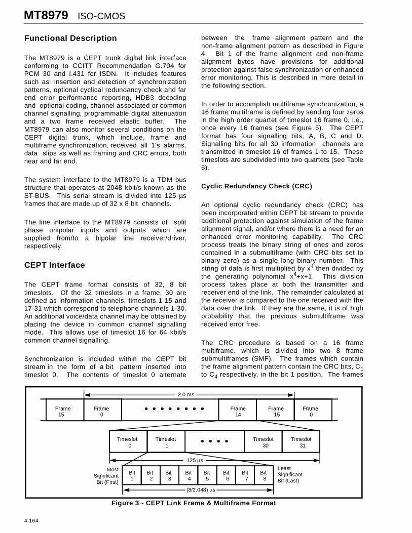
The MT8979 is a CEPT trunk digital link interfaceconforming to CCITT Recommendation G.704 forPCM 30 and I.431 for ISDN. It includes featuressuch as: insertion and detection of synchronizationpatterns, optional cyclical redundancy check and farend error performance reporting, HDB3 decodingand optional coding, channel associated or commonchannel signalling, programmable digital attenuationand a two frame received elastic buffer. TheMT8979 can also monitor several conditions on theCEPT digital trunk, which include, frame andmultiframe synchronization, received all 1’s alarms,data slips as well as framing and CRC errors, bothnear and far end.
The system interface to the MT8979 is a TDM busstructure that operates at 2048 kbit/s known as theST-BUS. This serial stream is divided into 125 µsframes that are made up of 32 x 8 bit channels.
The line interface to the MT8979 consists of splitphase unipolar inputs and outputs which aresupplied from/to a bipolar line receiver/driver,respectively.
CEPT Interface
The CEPT frame format consists of 32, 8 bittimeslots. Of the 32 timeslots in a frame, 30 aredefined as information channels, timeslots 1-15 and17-31 which correspond to telephone channels 1-30.An additional voice/data channel may be obtained byplacing the device in common channel signallingmode. This allows use of timeslot 16 for 64 kbit/scommon channel signalling.
Synchronization is included within the CEPT bitstream in the form of a bit pattern inserted intotimeslot 0. The contents of timeslot 0 alternate
between the frame alignment pattern and thenon-frame alignment pattern as described in Figure4. Bit 1 of the frame alignment and non-framealignment bytes have provisions for additionalprotection against false synchronization or enhancederror monitoring. This is described in more detail inthe following section.
In order to accomplish multiframe synchronization, a16 frame multiframe is defined by sending four zerosin the high order quartet of timeslot 16 frame 0, i.e.,once every 16 frames (see Figure 5). The CEPTformat has four signalling bits, A, B, C and D.Signalling bits for all 30 information channels aretransmitted in timeslot 16 of frames 1 to 15. Thesetimeslots are subdivided into two quartets (see Table6).
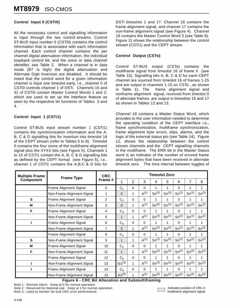
Cyclic Redundancy Check (CRC)
An optional cyclic redundancy check (CRC) hasbeen incorporated within CEPT bit stream to provideadditional protection against simulation of the framealignment signal, and/or where there is a need for anenhanced error monitoring capability. The CRCprocess treats the binary string of ones and zeroscontained in a submultiframe (with CRC bits set tobinary zero) as a single long binary number. Thisstring of data is first multiplied by x4 then divided bythe generating polynomial x4+x+1. This divisionprocess takes place at both the transmitter andreceiver end of the link. The remainder calculated atthe receiver is compared to the one received with thedata over the link. If they are the same, it is of highprobability that the previous submultiframe wasreceived error free.
The CRC procedure is based on a 16 framemultiframe, which is divided into two 8 framesubmultiframes (SMF). The frames which containthe frame alignment pattern contain the CRC bits, C1to C4 respectively, in the bit 1 position. The frames
Figure 3 - CEPT Link Frame & Multiframe Format
Frame15 0 14 15 0
Timeslot0 1 30 31
MostSignificantBit (First)
LeastSignificantBit (Last)
Bit1 2 3 4 5 6 7 8
FrameFrameFrameFrame
Timeslot Timeslot Timeslot
Bit Bit Bit Bit Bit BitBit
2.0 ms
(8/2.048) µs
125 µs
• • • • • • • •
• • • •

ISO-CMOS MT8979
4-165
which contain the non-frame alignment patterncontain within the bit 1 position, a 6 bit CRCmultiframe alignment signal and two spare bits (inframes 13 and 15), which are used for CRC errorperformance reporting (refer to Figure 6). During theCRC encoding procedure the CRC bit positions areinitially set at zero. The remainder of the calculationis stored and inserted into the respective CRC bits ofthe next SMF. The decoding process repeats themultiplication division process and compares theremainder with the CRC bits received in the nextSMF.
The two spare bits (denoted Si1 and Si2 in Figure 6)in the CRC-4 multiframe are used to monitor far-enderror performance. The results of the CRC-4comparisons for the previously received SMFII andSMFI are encoded and transmitted back to the farend in the Si bits (refer to Table 1).
ST-BUS Interface
The ST-BUS is a synchronous time divisionmultiplexed serial bus with data streams operating at2048 kbit/s and configured as 32, 64 kbit/s channels(refer Figure 7). Synchronization of the data transferis provided from a frame pulse, which identifies theframe boundaries and repeats at an 8 kHz rate.Figure 17 shows how the frame pulse (F0i) definesthe ST-BUS frame boundaries. All data is clockedinto the device on the falling edge of the 2048 kbit/sclock (C2i), while data is clocked out on the risingedge of the 2048 kbit/s clock at the start of the bitcell.
Table 1. Coding of Spare Bits Si1 and Si2
Data Input (DSTi)
The MT8979 receives information channels on theDSTi pin. Of the 32 available channels on thisserial input, 30 are defined as information channels.They are channels 1-15 and 17-31. These 30timeslots are the 30 telephone channels of the CEPTformat numbered 1-15 and 16-30. Timeslot 0 and 16are unused to allow the synchronization andsignalling information to be inserted, from the ControlStreams (CSTi0 and CSTi1). The relationshipbetween the input and output ST-BUS stream andthe CEPT line is illustrated in Figures 8 to 12. Incommon channel signalling mode timeslot 16becomes an active channel. In this mode channel 16on DSTi is transmitted on timeslot 16 of the CEPTlink unaltered. This mode is activated by bit 5 ofchannel 31 of CSTi0.
Si1 bit(frame
13)
Si2 bit(frame
15)Meaning
1 1 CRC results for both SMFI, II areerror free.
1 0 CRC result for SMFII is in error.CRC result for SMFI is error free.
0 1 CRC result for SMFII is error free.CRC result for SMFI is in error.
0 0 CRC results for both SMFI, II arein error.
Figure 4 - Allocation of Bits in Timeslot 0 of the CEPT LinkNote 1 : With CRC active, this bit is ignored.Note 2 : With SiMUX active, this bit transmits SMF CRC results in frames 13 and 15Note 3 : Reserved for National use
.
Figure 5 - Allocation of Bits in Timeslot 16 of the CEPT Link
Bit Number
1 2 3 4 5 6 7 8
Timeslot 0 containing the frame alignment signal
Reserved for International use (1)
0 0 1 1 0 1 1
Timeslot 0 containing the non-frame alignment signal
Reserved for International use (2)
1 Alarm indication to the remote PCM multiplex equipment
SeeNote#3
SeeNote#3
SeeNote#3
SeeNote#3
SeeNote#3
Timeslot 16 of frame 0 Timeslot 16 of frame 1
• • •
Timeslot 16 of frame 15
0000 XYXX
ABCD bits for telephone channel 1
(timeslot 1)
ABCD bits for telephone channel 16
(timeslot 17)
ABCD bits for telephone channel 15
(timeslot 15)
ABCD bits for telephone channel 30
(timeslot 31)
MT8979 ISO-CMOS
4-166
Control Input 0 (CSTi0)
All the necessary control and signalling informationis input through the two control streams. ControlST-BUS input number 0 (CSTi0) contains the controlinformation that is associated with each informationchannel. Each control channel contains the perchannel digital attenuation information, the individualloopback control bit, and the voice or data channelidentifier, see Table 2. When a channel is in datamode (B7 is high) the digital attenuation andAlternate Digit Inversion are disabled. It should benoted that the control word for a given informationchannel is input one timeslot early, i.e., channel 0 ofCSTi0 controls channel 1 of DSTi. Channels 15 and31 of CSTi0 contain Master Control Words 1 and 2,which are used to set up the interface feature asseen by the respective bit functions of Tables 3 and4.
Control Input 1 (CSTi1)
Control ST-BUS input stream number 1 (CSTi1)contains the synchronization information and the A,B, C & D signalling bits for insertion into timeslot 16of the CEPT stream (refer to Tables 5 to 8). Timeslot0 contains the four zeros of the multiframe alignmentsignal plus the XYXX bits (see Figure 5). Channels 1to 15 of CSTi1 contain the A, B, C & D signalling bitsas defined by the CEPT format (see Figure 5), i.e.,channel 1 of CSTi1 contains the A,B,C & D bits for
DSTi timeslots 1 and 17. Channel 16 contains theframe alignment signal, and channel 17 contains thenon-frame alignment signal (see Figure 4). Channel18 contains the Master Control Word 3 (see Table 9).Figure 11 shows the relationship between the controlstream (CSTi1) and the CEPT stream.
Control Output (CSTo)
Control ST-BUS output (CSTo) contains themultiframe signal from timeslot 16 of frame 0 (seeTable 10). Signalling bits A, B, C & D for each CEPTchannel are sourced from timeslot 16 of frames 1-15and are output in channels 1-15 on CSTo , as shownin Table 11. The frame alignment signal andnonframe alignment signal, received from timeslot 0of alternate frames, are output in timeslots 16 and 17as shown in Tables 12 and 13.
Channel 18 contains a Master Status Word, whichprovides to the user information needed to determinethe operating condition of the CEPT interface i.e.,frame synchronization, multiframe synchronization,frame alignment byte errors, slips, alarms, and thelogic of the external status pin (see Table 14). Figure12, shows the relationship between the controlstream channels and the CEPT signalling channelsin the multiframe. The ERR bit in the Master Statusword is an indicator of the number of errored framealignment bytes that have been received in alternatetimeslot zero. The time interval between toggles of
Figure 6 - CRC Bit Allocation and SubmultiframingNote 1 : Remote Alarm. Keep at 0 for normal operation.Note 2 : Reserved for National use. Keep at 1 for normal operation.Note 3 : Used to monitor far-end CRC error performance.
Multiple Frame Component Frame Type CRC
Frame #Timeslot Zero
1 2 3 4 5 6 7 8
Frame Alignment Signal 0 C1 0 0 1 1 0 1 1
Non-Frame Alignment Signal 1 0 1 A(1) Sn(2) Sn(2) Sn(2) Sn(2) Sn(2)
S Frame Alignment Signal 2 C2 0 0 1 1 0 1 1
M Non-Frame Alignment Signal 3 0 1 A(1) Sn(2) Sn(2) Sn(2) Sn(2) Sn(2)
F Frame Alignment Signal 4 C3 0 0 1 1 0 1 1
Non-Frame Alignment Signal 5 1 1 A(1) Sn(2) Sn(2) Sn(2) Sn(2) Sn(2)
I Frame Alignment Signal 6 C4 0 0 1 1 0 1 1
Non-Frame Alignment Signal 7 0 1 A(1) Sn(2) Sn(2) Sn(2) Sn(2) Sn(2)
Frame Alignment Signal 8 C1 0 0 1 1 0 1 1
S Non-Frame Alignment Signal 9 1 1 A(1) Sn(2) Sn(2) Sn(2) Sn(2) Sn(2)
M Frame Alignment Signal 10 C2 0 0 1 1 0 1 1
F Non-Frame Alignment Signal 11 1 1 A(1) Sn(2) Sn(2) Sn(2) Sn(2) Sn(2)
Frame Alignment Signal 12 C3 0 0 1 1 0 1 1
I Non-Frame Alignment Signal 13 Si1(3) 1 A(1) Sn(2) Sn(2) Sn(2) Sn(2) Sn(2)
I Frame Alignment Signal 14 C4 0 0 1 1 0 1 1
Non-Frame Alignment Signal 15 Si2(3) 1 A(1) Sn(2) Sn(2) Sn(2) Sn(2) Sn(2)
indicates position of CRC-4multiframe alignment signal

ISO-CMOS MT8979
4-167
Figure 7 - ST-BUS Stream Format
CHANNEL31 0 30
BIT
CHANNEL CHANNEL CHANNEL CHANNEL31 0
BIT BIT BIT BIT BIT BIT BIT
• • •
LeastSignificantBit (Last)
MostSignificantBit (First)
(8/2.048)µs
125µs
7 6 5 4 3 2 1 0
the ERR bit can be used to evaluate the bit errorrate of the line according to the CCITTRecommendation G.732 (see section on FrameAlignment Error Counter).
Channel 19 contains the Phase Status Word (seeTable 15), which can be used to determine the phaserelationship between the ST-BUS frame pulse (F0i)and the rising edge of E8Ko. This information couldbe used to determine the long term trend of thereceived data rate, or to identify the direction of aslip.
Channel 20 contains the CRC error count (see Table16). This counter will wrap around once terminalcount is achieved (256 errors). If the maintenanceoption is selected (bit 3 of MCW3) the counter isreset once per second.
Channel 21 contains the Master Status Word 2 (seeTable 17). This byte identifies the status of the CRCreframe and CRC sync. It also reports the Si bitsreceived in timeslot 0 of frames 13 and 15 andthe ninth and most significant bit (b8) of the 9-bitPhase Status Word.
Elastic Buffer
The MT8979 has a two frame elastic buffer at thereceiver, which absorbs the jitter and wander in thereceived signal. The received data is written into theelastic buffer with the extracted E2i (2048 kHz) clockand read out of the buffer on the ST-BUS side withthe system C2i (2048 kHz) clock (e.g., PBX systemclock). Under normal operating conditions, in asynchronous network, the system C2i clock isphase-locked to the extracted E2i clock. In thissituation every write operation to the elastic buffer isfollowed by a read operation. Therefore, underflowor overflow of data in the elastic buffer will not occur.
If the system clock is not phase-locked to theextracted clock (e.g., lower quality link which is not
selected as the clock source for the PBX) then thedata rate at which the data is being written into thedevice on the line side may differ from the rate atwhich it is being read out on the ST-BUS side.
When the clocks are not phase-locked, twosituations can occur:
Case #1: If the data on the line side is being writtenin at a rate SLOWER than it is being read out on theST-BUS side, the distance between the write pointerand the read pointer will begin to decrease over time.When the distance is less than two channels, thebuffer will perform a controlled slip which will movethe read pointers to a new location 34 channelsaway from the write pointer. This will result in theREPETITION of the received frame.
Case #2: If the data on the line side is being writtenin at a rate FASTER than it is being read out on theST-BUS side, the distance between the write pointerand the read pointer will begin to increase over time.When the distance exceeds 42 channels, the elasticbuffer will perform a controlled slip which will movethe read pointer to a new location ten channels awayfrom the write pointer. This will result in the LOSS ofthe last received frame.
Note that when the device performs a controlled slip,the ST-BUS address pointer is repositioned so thatthere is either a 10 channel or 34 channel delaybetween the input CEPT frame and the outputST-BUS frame. Since the buffer performs acontrolled slip only if the delay exceeds 42 channelsor is less than two channels, there is a minimumeight channel hysteresis built into the slipmechanism. The device can, therefore, absorb eightchannels or 32.5µs of jitter in the received signal.
There is no loss of frame synchronization, multiframesynchronization or any errors in the signalling bitswhen the device performs a slip.

MT8979 ISO-CMOS
4-168
Fig
ure
8 -
Re
latio
nsh
ip b
etw
een
Inp
ut
DS
Ti C
han
nels
an
d T
ran
smitt
ed C
EP
T T
ime
slo
ts
Fig
ure
9 -
Rel
atio
nsh
ip b
etw
een
Rec
eive
d C
EP
T T
imes
lots
an
d O
utp
ut D
STo
Ch
ann
els
Fig
ure
10
- R
elat
ion
ship
bet
wee
n In
put
CS
Ti0
Cha
nnel
s an
d C
on
tro
lled
CE
PT
Tim
eslo
ts
Fig
ure
11
- R
ela
tions
hip
bet
wee
n In
put
CS
Ti1
Ch
ann
els
an
d Tr
ansm
itte
d C
EP
T F
ram
es
Fig
ure
12-
Re
latio
nshi
p b
etw
een
Re
ceiv
ed C
EP
T F
ram
es
and
Ou
tput
CS
To C
hann
els
- *D
enot
es U
nus
ed C
han
nel (
CS
To o
utp
ut
is n
ot
put
in h
igh
impe
danc
e st
ate
)-C
CS
Den
ote
s S
igna
llin
g C
hann
el if
Com
mon
Ch
anne
l Sig
nalli
ng M
ode
Sel
ecte
d-
A D
en
ote
s F
ram
e-A
lign
me
nt
Fra
me
-S1
Den
otes
Mas
ter
Sta
tus
Wor
d 1
(M
SW
1)
- N
De
no
tes
No
n F
ram
e-A
lign
me
nt
Fra
me
-S2
Den
otes
Ph
ase
Sta
tus
Wo
rd (
PS
W)
- C
1, C
2, C
3 D
enot
es M
aste
r C
ont
rol W
ord
s 1,
2,3
-S3
Den
otes
CR
C E
rro
r C
oun
t-
SIG
De
note
s S
igna
llin
g C
han
nel
-S4
Den
otes
Mas
ter
Sta
tus
Wor
d 2
(M
SW
2)
DS
Ti
Cha
nnel
#0
12
34
56
78
910
1112
1314
1516
1718
1920
2122
2324
2526
2728
2930
31
CE
PT
T
imes
lot #
12
34
56
78
910
1112
1314
15C
CS
1718
1920
2122
2324
2526
2728
2930
31
DS
Ti
Cha
nnel
#0
12
34
56
78
910
1112
1314
1516
1718
1920
2122
2324
2526
2728
2930
31
CE
PT
T
imes
lot #
01
23
45
67
89
1011
1213
1415
SIG
1718
1920
2122
2324
2526
2728
2930
31
CS
Ti0
Cha
nnel
#0
12
34
56
78
910
1112
1314
1516
1718
1920
2122
2324
2526
2728
2930
31
Dev
ice
Con
trol
C1
C2
CE
PT
Cha
nnel
#
Con
trol
Wor
d1
23
45
67
89
1011
1213
1415
1718
1920
2122
2324
2526
2728
2930
31
CS
Ti1
Cha
nnel
#0
12
34
56
78
910
1112
1314
1516
1718
1920
2122
2324
2526
2728
2930
31
Dev
ice
Con
trol
C3
**
**
**
**
**
**
*C
EP
TF
RA
ME
#C
HA
NN
EL
#0 16
1 162 16
3 164 16
5 166 16
7 168 16
9 1610 16
11 1612 16
13 1614 16
15 16A 0
N 0
CS
ToC
hann
el #
01
23
45
67
89
1011
1213
1415
1617
1819
2021
2223
2425
2627
2829
3031
Dev
ice
Sta
tus
S1
S2
S3
S4
**
**
**
**
**
CE
PT
FR
AM
E #
TIM
ES
LOT
#0 16
1 162 16
3 164 16
5 166 16
7 168 16
9 1610 16
11 1612 16
13 1614 16
15 16A 0
N 0
ISO-CMOS MT8979
4-169
Frame Alignment Error Counter
The MT8979 provides an indication of the bit errorrate found on the link as required by CCITTRecommendation G.703. The ERR bit (Bit 5 ofMSW1) is used to count the number of errors foundin the frame alignment signal and this can be used toestimate the bit error rate. The ERR bit changesstate when 16 errors have been detected in theframe alignment signal. This bit can not change statemore than once every 128 ms, placing an upper limiton the detectable error rate at approximately 10-3.The following formula can be used to calculate theBER:
where:7 - is the number of bits in the frame alignment
signal (0011011).16 - is the number of errored frame alignment
signals counted between changes of stateof the ERR bit.
4000 - is the number of frame alignment signals ina one second interval.
This formula provides a good approximation of theBER given the following assumptions:
1. The bit errors are uniformly distributed on theline. In other words, every bit in every channel isequally likely to get an error.
2. The errors that occur in channel 0 are bit errors.If the first assumption holds and the bit error rateis reasonable, (below 10-3) then the probability oftwo or more errors in seven bits is very low.
Attenuation ROM
All transmit and receive data in the MT8979 ispassed through the digital attenuation ROMaccording to the values set on bits 5 - 0 of datachannels in the control stream (CSTi0). Data can beattenuated on a per-channel basis from 1 to -6 dB forboth Tx and Rx data (refer Table 2).
Digital attenuation is applied on a per-channel basisto the data found one channel after the controlinformation stored in the control channel CSTi0, i.e.,control stream 0 channel 4 contains the attenuationsetting for data stream (DSTo) channel 5.
BER= 16* number of times ERR bit toggles
7 * 4000 * elapsed time in seconds
Signalling Bit RAM
The A, B, C, & D Bit RAM is used to retain the statusof the per-channel signalling bits so that they may bemultiplexed into the Control Output Stream (CSTo).This signalling information is only valid when themodule is synchronized to the received data stream.If synchronization is lost, the status of the signallingbits will be retained for 6.0 ms provided the signallingdebounce is active.
Integrated into the signalling bit RAM is a debouncecircuit which will delay valid signalling bit changes for6.0 to 8.0 ms. By debouncing the signalling bits, abit error will not affect the call in progress. (See Table3, bits 3-0 of channel 15 on the CSTi0 line.)
CEPT PCM 30 Format MUX
The CEPT Link Multiplexer formats the data streamcorresponding to the CEPT PCM 30 format. Thisimplies that the multiplexer will use timeslots 1 to 15and 17 to 31 for data and uses timeslots 0 & 16 forthe synchronization and channel associatedsignalling.
The frame alignment or non-frame alignment signalsfor timeslot zero are sourced by the control streaminput CSTi1 channel 16 and 17, respectively. Themost significant bit of timeslot zero will optionallycontain the cyclical redundancy check, CRCmultiframe pattern and Si bits used for far-end CRCmonitoring.
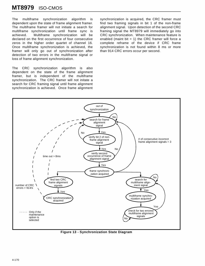
Framing Algorithms
There are three distinct framers within the MT8979.These include a frame alignment signal framer, amultiframe framer and a CRC framer. Figure 13shows the state diagram of the framing algorithms.The dotted lines shows optional features, which areenabled in the maintenance mode.
The frame synchronization circuit searches for thefirst frame alignment signal within the bit stream.Once detected, the frame counters are set to find thenon-frame alignment signal. If bit 2 of the non-framealignment signal is not one, a new search is initiated,else the framer will monitor for the frame alignmentin the next frame. If the frame alignment signal isfound, the device immediately declares framesynchronization.
MT8979 ISO-CMOS
4-170
The multiframe synchronization algorithm isdependent upon the state of frame alignment framer.The multiframe framer will not initiate a search formultiframe synchronization until frame sync isachieved. Multiframe synchronization will bedeclared on the first occurrence of four consecutivezeros in the higher order quartet of channel 16.Once multiframe synchronization is achieved, theframer will only go out of synchronization afterdetection of two errors in the multiframe signal orloss of frame alignment synchronization.
The CRC synchronization algorithm is alsodependent on the state of the frame alignmentframer, but is independent of the multiframesynchronization. The CRC framer will not initate asearch for CRC framing signal until frame alignmentsynchronization is achieved. Once frame alignment
synchronization is acquired, the CRC framer mustfind two framing signals in bit 1 of the non-framealignment signal. Upon detection of the second CRCframing signal the MT8979 will immediately go intoCRC synchronization. When maintenance feature isenabled (maint bit = 1) the CRC framer will force acomplete reframe of the device if CRC framesynchronization is not found within 8 ms or morethan 914 CRC errors occur per second.
Figure 13 - Synchronization State Diagram
out ofsynchronization
search for framealignment
signal
verify bit 2 of non-frame alignment
signal
verify secondoccurrence of frame
alignment signal
find two CRCframe alignment
CRC synchronizationacquired
search formultiframe align-
ment signal
multiframe synchro-nization acquired
check for two erroredmultiframe alignment
signals
No
No
Yes
Yes
Yes
Yes
Yes
Yes
No
# of consecutive incorrectframe alignment signals = 3
time out > 8ms
No
- - - - - Only if the maintenanceoption isselected
signals
No
number of CRCerrors > 914/s
frame synchroni-zation acquired

ISO-CMOS MT8979
4-171
Table 2. Per Channel Control Word: Data Format for CSTi0 Channels 0-14, and 16-30
Table 3. Master Control 1 (MCW1): Data Format for CSTi0 Channel 15
BIT NAME DESCRIPTION
7 DATA Data Channel: If ‘1‘, then the controlled timeslot on the CEPT 2048 kbit/s link is treated as a data channel; i.e., no ADI encoding or decoding is performed on transmission or reception, and digital attenuation is disabled.If ‘0‘, then the state of the ADI pin determines whether or not ADI encoding and decoding is performed.
6 LOOP Per-Channel Loopback: If ‘1‘, then the controlled timeslot on the transmitted CEPT 2048 kbit/s link is looped internally to replace the data on the corresponding received timeslot. If ‘0‘, then this function is disabled. This function only operates if frame synchronization is received from the CEPT link. If more than one channel is looped per frame only the first one will be active.
5,4,3 RXPAD4,2,1 Receive Attenuation Pad: Per timeslot receive attenuation control bits.
RXPAD400001111
RXPAD200110011
RXPAD101010101
Gain (dB)0-1-2-3-4-5-61
2,1,0 TXPAD4,2,1 Transmit Attenuation Pad: Per timeslot transmit attenuation control bits.
TXPAD400001111
TXPAD200110011
TXPAD101010101
Gain (dB)0-1-2-3-4-5-61
BIT NAME DESCRIPTION
7 (N/A) Keep at ‘1‘ for normal operation.
6 LOOP16 Channel 16 Loopback: If ‘1‘, then timeslot 16 on the transmitted CEPT 2048 kbit/s link is looped internally to replace the data received on timeslot 16.If ‘0,‘ then this function is disabled.This function only operates if frame synchronization is received from the CEPT link and only a single timeslot can be looped within the frame.
5,4 (N/A) Keep at ‘1‘ for normal operation.
3,2,1
& 0
NDBD, NDBC,NDBB
& NDBA
Signalling Bit Debounce: If ‘1‘, then no debouncing is applied to the received A, B, C or D signalling bits. If ‘0‘, then the received A, B, C or D signalling bits are debounced for between 6 and 8 ms.

MT8979 ISO-CMOS
4-172
Table 4. Master Control 2 (MCW2): Data Format for CSTi0 Channel 31
Table 5. Multiframe Alignment Signal: Data Format for CSTi1 Channel 0on the Transmitted CEPT Link
BIT NAME DESCRIPTION
7 (N/A) Keep at ‘1‘ for normal operation.
6 (N/A) Keep at ‘0‘ for normal operation.
5 CCS Common Channel Signalling: If 1, then the MT8979 operates in its common channel signalling mode. Channel 16 on the DSTi pin is transmitted on timeslot 16 of the CEPT link, and timeslot 16 from the received CEPT link is output on channel 16 on the DSTo pin. Channel 15 on the CSTi0 pin contains the information for the control of timeslot 16. Channels 0 to 15 on CSTi1 and CSTo are unused.If ‘0‘, the device is in channel associated signalling mode where channel 16 is used to transmit the ABCD signalling bits.
4 8KHzSEL 8KHz Select: If ‘1‘, then an 8 kHz signal synchronized to the received CEPT 2048 kbit/s link is output on the E8Ko pin. This feature is only valid when frame synchronization is received from the CEPT link.If ‘0‘, then the E8Ko pin goes into its high impedance state.
3 TXAIS Transmit Alarm Indication Signal: If ‘1‘, then an all 1’ s alarm signal is transmitted on all timeslots.If ‘0‘, then the timeslots functions normally.
2 TXTS16AIS Transmit Timeslot 16 Alarm Indication Signal: If ‘1‘, then an all 1’s alarm signal is transmitted on timeslot 16.If ‘0‘, then timeslot 16 functions normally.
1 XCTL External Control:If ‘1‘, then the XCtl pin is driven high.If ‘0‘, then the XCtl pin is driven low.
0 (N/A) (unused)
BIT NAME DESCRIPTION
7-4 MA1-4 Transmit Multiframe Alignment Bits 1 to 4: These bits are transmitted on the CEPT2048 kbit/s link in bit positions 1 to 4 of timeslot 16 of frame 0 of the multiframe. Theyshould be kept at ‘0‘ to allow multiframe alignment to be detected.
3 X1 This bit is transmitted on the CEPT 2048 kbit/s link in bit position 5 of timeslot 16 offrame 0 of the multiframe. It is a spare bit which should be kept at ‘1‘ if unused.
2 Y This bit is transmitted on the CEPT 2048 kbit/s link in bit position 6 of timeslot 16 offrame 0 of the multiframe. It is used to indicate the loss of multiframe alignment to theremote end of the link. A ‘1‘ on this bit is the signal that multiframe alignment on thereceived link has been lost. A ‘0’ indicates that multiframe alignment is detected.
1,0 X2,X3 These bits are transmitted on the CEPT 2048 kbit/s link in bit positions 7 and 8respectively, of timeslot 16 of frame 0 of the multiframe. They are spare bits whichshould be kept at ‘1‘ if unused.

ISO-CMOS MT8979
4-173
Table 6. Channel Associated Signalling: Data Format for CSTi1 Channels 1 to 15
Table 7. Frame Alignment Signal: Data Format for CSTi1 Channel 16
BIT NAME DESCRIPTION
7,6,5
& 4
A(N),B(N),C(N)
& D(N)
Transmit Signalling Bits for Channel N: These bits are transmitted on the CEPT 2048 kbit/s link in bit positions 1 to 4 of timeslot 16 in frame N, and are the A, B, C and D signalling bits associated with telephone channel N. The value of N lies in the range 1 to 15 and refers to the channel on the CSTi1 channel from which the bits are sourced, the telephone channel with which the bits are associated and the frame on the CEPT link on which the bits are transmitted. For example, the bits input on the CSTi1 pin on channel 3 are associated with telephone channel 3, which is timeslot 3 of the CEPT link, and are transmitted on bits positions 1 to 4 of timeslot 16 in frame 3 of each multiframe on the CEPT link . If bits B, C or D are not used they should be given the values ‘1, 0‘ and ‘1‘ respectively. The combination ‘0000‘ for ABCD bits should not be used for telephone channels 1 to 15 as this would interfere with multiframe alignment.
3,2,1
& 0
A(N+15),B(N+15),C(N+15)
& D(N+15)
Transmit Signalling Bits for Channel N+15: These bits are transmitted on the CEPT 2048 kbit/s link in bit positions 5 to 8 of timeslot 16 in frame N, and are the A, B, C and D signalling bits associated with telephone channel N+15. The value of N lies in the range 1 to 15 and refers to both the channel on the CSTi1 stream where the bits are supplied and the frame on the CEPT link on which the bits are transmitted, and indirectly indicates the telephone channel with which the bits are are associated. For example, the bits input on the CSTi1 pin on channel 3 are associated with telephone channel 18, which is timeslot 19 of the CEPT link, and are transmitted in bits positions 5 to 8 of timeslot 16 in frame 3 of each multiframe on the CEPT link .
BIT NAME DESCRIPTION
7 IU0 International Use 0: When CRC is disabled, this bit is transmitted on the CEPT 2048 kbit/s link in bit position 1 of timeslot 0 of frame-alignment frames . It is reserved for international use and should be kept at ‘1’ when not used. If CRC is enabled, this bit is not used.
6-0 FAF2-8 Transmit Frame Alignment Frame Bits 2 to 8: These bits are transmitted on the CEPT 2048 kbit/s link in bit positions 2 to 8 of timeslot 0 of frame-alignment frames. These bits form the frame alignment signal and should be set to ‘0011011‘.
MT8979 ISO-CMOS
4-174
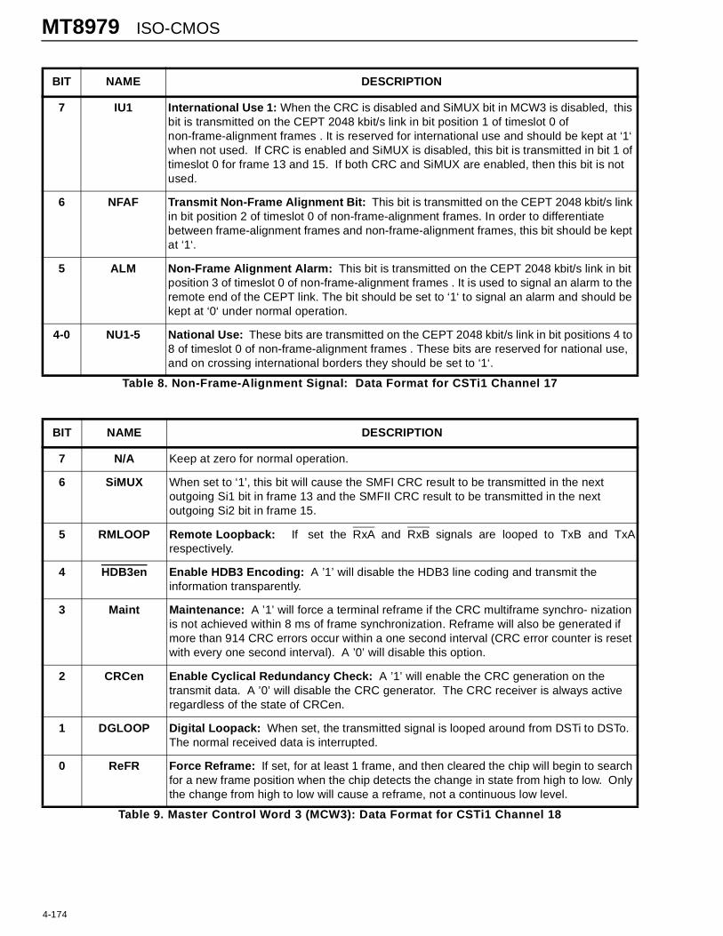
Table 8. Non-Frame-Alignment Signal: Data Format for CSTi1 Channel 17
Table 9. Master Control Word 3 (MCW3): Data Format for CSTi1 Channel 18
BIT NAME DESCRIPTION
7 IU1 International Use 1: When the CRC is disabled and SiMUX bit in MCW3 is disabled, this bit is transmitted on the CEPT 2048 kbit/s link in bit position 1 of timeslot 0 of non-frame-alignment frames . It is reserved for international use and should be kept at ‘1‘ when not used. If CRC is enabled and SiMUX is disabled, this bit is transmitted in bit 1 of timeslot 0 for frame 13 and 15. If both CRC and SiMUX are enabled, then this bit is not used.
6 NFAF Transmit Non-Frame Alignment Bit: This bit is transmitted on the CEPT 2048 kbit/s link in bit position 2 of timeslot 0 of non-frame-alignment frames. In order to differentiate between frame-alignment frames and non-frame-alignment frames, this bit should be kept at ‘1‘.
5 ALM Non-Frame Alignment Alarm: This bit is transmitted on the CEPT 2048 kbit/s link in bit position 3 of timeslot 0 of non-frame-alignment frames . It is used to signal an alarm to the remote end of the CEPT link. The bit should be set to ‘1‘ to signal an alarm and should be kept at ‘0‘ under normal operation.
4-0 NU1-5 National Use: These bits are transmitted on the CEPT 2048 kbit/s link in bit positions 4 to 8 of timeslot 0 of non-frame-alignment frames . These bits are reserved for national use, and on crossing international borders they should be set to ‘1‘.
BIT NAME DESCRIPTION
7 N/A Keep at zero for normal operation.
6 SiMUX When set to ‘1’, this bit will cause the SMFI CRC result to be transmitted in the next outgoing Si1 bit in frame 13 and the SMFII CRC result to be transmitted in the next outgoing Si2 bit in frame 15.
5 RMLOOP Remote Loopback: If set the RxA and RxB signals are looped to TxB and TxArespectively.
4 HDB3en Enable HDB3 Encoding: A ’1’ will disable the HDB3 line coding and transmit the information transparently.
3 Maint Maintenance: A ’1’ will force a terminal reframe if the CRC multiframe synchro- nization is not achieved within 8 ms of frame synchronization. Reframe will also be generated if more than 914 CRC errors occur within a one second interval (CRC error counter is reset with every one second interval). A ’0’ will disable this option.
2 CRCen Enable Cyclical Redundancy Check: A ’1’ will enable the CRC generation on the transmit data. A ’0’ will disable the CRC generator. The CRC receiver is always active regardless of the state of CRCen.
1 DGLOOP Digital Loopack: When set, the transmitted signal is looped around from DSTi to DSTo. The normal received data is interrupted.
0 ReFR Force Reframe: If set, for at least 1 frame, and then cleared the chip will begin to search for a new frame position when the chip detects the change in state from high to low. Only the change from high to low will cause a reframe, not a continuous low level.

ISO-CMOS MT8979
4-175
Table 10. Received Multiframe Alignment Signal: Data Format for CSTo Channel 0
Table 11. Received Channel Associated Signalling: Data Format for CSTo Channels 1 to 15
Table 12. Received Frame Alignment Signal: Data Format for CSTo Channel 16
BIT NAME DESCRIPTION
7-4 MA1-4 Receive Multiframe Alignment Bits 1 to 4: These are the bits which are receivedfrom the CEPT 2048 kbit/s link in bit positions 1 to 4 of timeslot 16 of frame 0 of themultiframe. They should all be ‘0‘.
3 X1 This is the bit which is received on the CEPT 2048 kbit/s link in bit position 5 oftimeslot 16 of frame 0 of the multiframe. It is a spare bit which should be ‘1‘ if unused.It is not debounced.
2 Y This is the bit which is received on the CEPT 2048 kbit/s link in bit position 6 oftimeslot 16 of frame 0 of the multiframe. It is used to indicate the loss of multiframealignment at the remote end of the link. A ‘1‘ on this bit is the signal that multiframealignment at the remote end of the link has been lost. A ‘0‘ indicates that multiframealignment is detected. It is not debounced.
1,0 X2,X3 These are the bits which are received on the CEPT 2048 kbit/s link in bit positions 7and 8 respectively, of timeslot 16 of frame 0 of the multiframe. They are spare bitswhich should be ‘1‘ if unused. They are not debounced.
BIT NAME DESCRIPTION
7,6,5
& 4
A(N),B(N),C(N)
& D(N)
Receive Signalling Bits for Channel N: These are the bits which are received from the CEPT 2048 kbit/s link in bit positions 1 to 4 of timeslot 16 in frame N (frame #), and are the A, B, C and D signalling bits associated with telephone channel N. The value of N lies in the range 1 to 15 and refers to the channel on the CSTo stream on which the bits are output, the telephone channel with which the bits are associated and the frame on the CEPT link on which the bits are received. For example, the bits output on the CSTo stream on channel 3 are associated with telephone channel 3, which is timeslot 3 of the CEPT link, and are received on bits positions 1 to 4 of timeslot 16 in frame 3 of each multiframe on the CEPT link . If bits B, C or D are not used they should have the values ‘1, 0‘ and ‘1‘ respectively. The combination ‘0000‘ for ABCD bits should not be found for telephone channels 1 to 15 as this implies interference with multiframe alignment.
3,2,1
& 0
A(N+15),B(N+15),C(N+15)
& D(N+15)
Receive Signalling Bits for Channel N+ 15: These are the bits which are received from the CEPT 2048 kbit/s link in bit positions 5 to 8 of timeslot 16 in frame N, and are the A, B, C and D signalling bits associated with telephone channel N+15. The value of N lies in the range 1 to 15 and refers to both the channel on the CSTo stream where the bits are output and the frame on the CEPT link on which the bits are received, and indirectly indicates the telephone channel with which the bits are are associated. The associated channel is N+15.For example, the bits output on the CSTo stream on channel 3 are associated with telephone channel 18, which is timeslot 19 of the CEPT link, and are received on bits positions 5 to 8 of timeslot 16 in frame 3 of each multiframe on the CEPT link .
BIT NAME DESCRIPTION
7 IU0 International Use 0: This is the bit which is received from the CEPT 2048 kbit/s link in bit position 1 of timeslot 0 of frame-alignment frames . It is reserved for the CRC remainder or for international use.
6-0 FAF2-8 Frame Alignment Signal Bits 2 to 8: These are the bits which are received from the CEPT 2048 kbit/s link in bit positions 2 to 8 of timeslot 0 of frame-alignment frames. These bits form the frame alignment signal and should have the values of ‘0011011‘.

MT8979 ISO-CMOS
4-176
Table 13. Received Non-Frame Alignment Signal: Data Format for CSTo Channel 17
Table 14. Master Status Word 1 (MSW1): Data Format for CSTo Channel 18
Table 15. Phase Status Word (PSW): Data Format for CSTo Channel 19
BIT NAME DESCRIPTION
7 IU1 International Use 1: This is the bit which is received from the CEPT 2048 kbit/s link in bit position 1 of timeslot 0 of non-frame-alignment frames . It is reserved for the CRC framing or as international bits.
6 NFAF Receive Non-Frame Alignment Bit: This is the bit which is received from the CEPT 2048 kbit/s link in bit position 2 of timeslot 0 of non-frame-alignment frames . This bit should be ‘1‘ in order to differentiate between frame-alignment frames and non-frame-alignment frames.
5 ALM Non-Frame Alignment Alarm: This is the bit which is received from the CEPT 2048 kbit/s link in bit position 3 of timeslot 0 of non-frame-alignment frames . It is used to signal an alarm from the remote end of the CEPT link. This bit should have the value ‘0‘ under normal operation and should go to ‘1 ‘to signal an alarm.
4-0 NU1-5 National Use: These are the bits which are received on the CEPT 2048 kbit/s link in bit positions 4 to 8 of timeslot 0 of non-frame-alignment frames . These bits are reserved for national use, and on crossing international borders they should have the value ‘1‘.
BIT NAME DESCRIPTION
7 TFSYN Frame Sync: This bit goes to ‘1‘ to indicate a loss of frame alignment synchronization by the MT8979. It goes to ‘0‘ when frame synchronization is detected.
6 MFSYN Multiframe Sync: This bit goes to ‘1‘ to indicate a loss of multiframe synchronization by the MT8979. It goes to ‘0‘ when multiframe synchronization is detected.
5 ERR Frame Alignment Error: This bit changes state when 16 or more errors have been detected in the frame alignment signal. It will not change state more than once every 128 ms.
4 SLIP Control Slip: This bit changes state when a slip occurs between the received CEPT 2048 kbit/s link and the 2048 kbit/s ST-BUS.
3 RXAIS Receive Alarm Indication Signal: This bit goes to ‘1‘ to signal that an all-ones alarm signal has been detected on the received CEPT 2048 kbit/s . It goes to ’0’ when the all-ones alarm signal is removed.
2 RXTS16AIS Receive Timeslot 16 Alarm Indication Signal: This bit goes to ‘1‘ to signal that an all-ones alarm signal has been detected on channel 16 of the received CEPT 2048 kbit/s link. It goes to ’0’ when the all-ones alarm signal is removed.
1 XS External Status: This bit contains the data sampled once per frame at the XS pin.
0 N/A (Unused).
BIT NAME DESCRIPTION
7 - 3 TxTSC Transmit Timeslot Count: The value of these five bits indicate the timeslot count between the ST-BUS frame pulse and the rising edge of E8Ko.
2 - 0 TxBTC Transmit Bit Count: The value of these three bits indicate the bit position within the timeslot count reported in TxTSC above.

ISO-CMOS MT8979
4-177
Table 16. CRC Error Count: Data Format for CSTo Channel 20
Table 17. Master Status Word 2 (MSW2): Data Format for CSTo Channel 21
BIT NAME DESCRIPTION
7 - 0 CERC CRC Error Counter: This byte is the CRC error counter. The counter will wrap around once it reaches FF count. If maintenance option is activated, the counter will reset after a one second interval.
BIT NAME DESCRIPTION
7 Si2 The received Si bit in frame 15 is reported in this bit. Si2 will be updated after each RxMF pulse (pin 23).
6 Si1 The received Si bit in frame 13 is reported in this bit. Si1 will be updated after each RxMF pulse (pin 23).
5-4 NA Unused.
3 CRCTimer CRC Timer: Transition from 1 to 0 indicates the start of one second interval in which CRC errors are accumulated. This bit stays high for 8 ms.
2 CRCRef CRC Reframe: A ’1’ indicates that the receive CRC multiframe synchronization could not be found within the time out period of 8 ms after detecting frame synchronization. This bit will go low if CRCSync goes low or if Maintenance is not activated.
1 CRCSync CRC Sync: A ’0’ indicates that CRC multiframing has been detected.
0 FrmPhase Frame Count: This is the ninth and most significant bit (b8) of the Phase Status Word (see Table 15). If the phase status word is incrementing, this bit will toggle when the phase reading exceeds ST-BUS channel 31, bit 7. If the phase word is decrementing, then this bit will toggle when the reading goes below ST-BUS channel 0, bit 0.
Applications
The MT8979 is only a link interface to the CEPTtrunk. As such, an external line driver and receiver isrequired along with an appropriate pulse transformerbefore being connected to the line.
Transmitter
In order to generate a bipolar line signal, the linkinterface to the MT8979 provides the user with twobipolar steering outputs, TxA and TxB. Thesecorrespond to the required positive and negative
pulses on the transmission line. Figure 14 shows arecommended output circuit for driving a line pulsetransformer.
The transistors are driven into saturation when theyare turned on, which applies a step function to thetransformer. The step input to the transformerproduces a nearly constant di/dt before the currentreaches steady state. By operating in the transientportion of the inductance response, the secondary ofthe transformer produces an almost square pulse.The base terminal of the transistors is AC coupled tothe MT8979 so that there is no DC path from VDD toground.
Figure 14 - Bipolar Line Driver
TxA
TxB
MT8979 •
•
• •
•
• •
••+12V
33µH
47µF
•
TIPo
RINGo
:.5
1.:
1.:
MT8979 ISO-CMOS
4-178
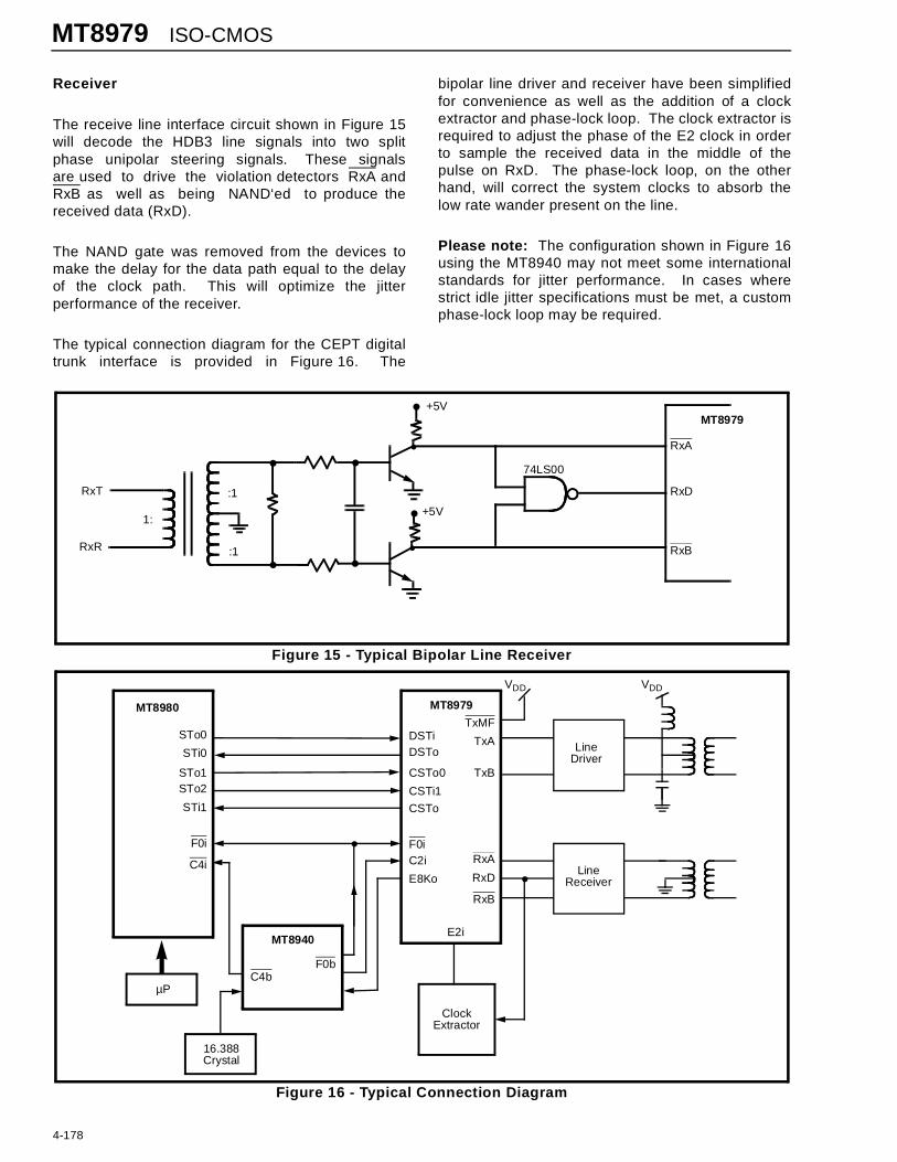
Receiver
The receive line interface circuit shown in Figure 15will decode the HDB3 line signals into two splitphase unipolar steering signals. These signalsare used to drive the violation detectors RxA andRxB as well as being NAND‘ed to produce thereceived data (RxD).
The NAND gate was removed from the devices tomake the delay for the data path equal to the delayof the clock path. This will optimize the jitterperformance of the receiver.
The typical connection diagram for the CEPT digitaltrunk interface is provided in Figure 16. The
bipolar line driver and receiver have been simplifiedfor convenience as well as the addition of a clockextractor and phase-lock loop. The clock extractor isrequired to adjust the phase of the E2 clock in orderto sample the received data in the middle of thepulse on RxD. The phase-lock loop, on the otherhand, will correct the system clocks to absorb thelow rate wander present on the line.
Please note: The configuration shown in Figure 16using the MT8940 may not meet some internationalstandards for jitter performance. In cases wherestrict idle jitter specifications must be met, a customphase-lock loop may be required.
Figure 15 - Typical Bipolar Line Receiver
Figure 16 - Typical Connection Diagram
RxT
RxR
RxA
RxD
RxB
MT8979
1:
:1
:1
+5V
+5V
74LS00
•
• •
•
•
•
•
•
MT8979
DSTiDSTo
CSTo0
CSTi1
CSTo
F0iC2i
E8Ko
TxMF
TxA
TxB
RxA
RxD
RxB
LineDriver
LineReceiver
ClockExtractor
16.388Crystal
MT8980
STo0
STi0
STo1STo2
STi1
F0i
C4i
µP
MT8940
C4bF0b
VDDVDD
•
•
E2i
ISO-CMOS MT8979
4-179
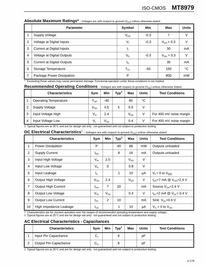
* Exceeding these values may cause permanent damage. Functional operation under these conditions is not implied.
‡ Typical figures are at 25°C and are for design aid only: not guaranteed and not subject to production testing.
† Characteristics are for clocked operation over the ranges of recommended operating temperature and supply voltage.‡ Typical figures are at 25°C and are for design aid only: not guaranteed and not subject to production testing.
‡ Typical figures are at 25°C and are for design aid only: not guaranteed and not subject to production testing.
Absolute Maximum Ratings* - Voltages are with respect to ground (VSS) unless otherwise stated.
Parameter Symbol Min Max Units
1 Supply Voltage VDD -0.3 7 V
2 Voltage at Digital Inputs VI -0.3 VDD + 0.3 V
3 Current at Digital Inputs II 30 mA
4 Voltage at Digital Outputs VO -0.3 VDD + 0.3 V
5 Current at Digital Outputs IO 30 mA
6 Storage Temperature TST -65 150 °C
7 Package Power Dissipation P 800 mW
Recommended Operating Conditions - Voltages are with respect to ground (VSS) unless otherwise stated.
Characteristics Sym Min Typ ‡ Max Units Test Conditions
1 Operating Temperature TOP -40 85 °C
2 Supply Voltage VDD 4.5 5 5.5 V
3 Input Voltage High VH 2.4 VDD V For 400 mV noise margin
4 Input Voltage Low VL VSS 0.4 V For 400 mV noise margin
DC Electrical Characteristics † - Voltages are with respect to ground (VSS) unless otherwise stated.
Characteristics Sym Min Typ ‡ Max Units Test Conditions
1 Power Dissipation P 40 88 mW Outputs unloaded
2 Supply Current IDD 8 16 mA Outputs unloaded
3 Input High Voltage VIH 2.0 VDD V
4 Input Low Voltage VIL 0 0.8 V
5 Input Leakage IIL 1 10 µA VI = 0 to VDD
6 Output High Voltage VOH 2.4 VDD V IOH=7 mA @ VOH=2.4 V
7 Output High Current IOH 7 20 mA Source VOH=2.4 V
8 Output Low Voltage VOL VSS 0.4 V IOL=2 mA @ VOL= 0.4 V
9 Output Low Current IOL 2 10 mA Sink VOL=0.4 V
10 High Impedance Leakage IOZ 1 10 µA VO = 0 to VDD
AC Electrical Characteristics - Capacitances
Characteristics Sym Min Typ ‡ Max Units Test Conditions
1 Input Pin Capacitance CI 8 pF
2 Output Pin Capacitance CO 8 pF

MT8979 ISO-CMOS
4-180
† Characteristics are for clocked operation over the ranges of recommended operating temperature and supply voltage.‡ Typical figures are at 25°C and are for design aid only: not guaranteed and not subject to production testing.* tSOD = 125 ns (max) over 0 - 70°C temperature range.
Figure 17 - Clock and Frame Alignment for 2048 kbit/s ST-BUS Streams
Figure 18 - Clock and Frame Timing for 2048 kbit/s ST-BUS Streams
AC Electrical Characteristics † - ST-BUS Timing (Figures 17 and 18)
Characteristics Sym Min Typ ‡ Max Units Test Conditions
1 C2i Clock Period tP20 400 488 600 ns
2 C2i Clock Width High or Low tW20 200 244 ns tP20 = 488 ns
3 Frame Pulse Setup Time tFPS 50 150 ns
4 Frame Pulse Hold Time tFPH 50 ns
5 Frame Pulse Width tFPW 100 300 ns
6 Serial Output Delay tSOD 150* ns 150 pF Load
7 Serial Input Setup Time tSIS 30 ns
8 Serial Input Hold Time tSIH 55 ns
9 Frame Pulse Setup Time 2 tFPS2 20 ns
F0i
C2i
ST-BUSBIT CELLS
Channel 31 Channel 0 Channel 0Bit 0 Bit 7 Bit 6
ST-BUSBit Stream
Bit Cell
F0i
C2i
DSTior CSTi0/1
DSToorCSTo
VIL
VIH
VIL
VIH
VIL
VIH
VOL
VOH
tFPStFPH
tFPW
tFPS2tP20
tSIS
tW20 tW20
tSIH
tSOD

ISO-CMOS MT8979
4-181
† Characteristics are for clocked operation over the ranges of recommended operating temperature and supply voltage.‡ Typical figures are at 25°C and are for design aid only: not guaranteed and not subject to production testing.* 256 tP20 - 100ns
Figure 19 - Functional Timing for Receive Multiframe Clocks
Figure 20 - Functional Timing for Transmit Multiframe Clock
Figure 21 - Clock and Frame Timing for 2048 kbit/s ST-BUS StreamsNote 1: These two signals do not have a defined phase relationship.
AC Electrical Characteristics † - Multiframe Clock Timing (Figure 21)
Characteristics Sym Min Typ ‡ Max Units Test Conditions
1 Receive Multiframe Output Delay tRMFD 150 ns 50 pF
2 Transmit Multiframe Setup Time tTMFS 50 ns
3 Transmit Multiframe Hold Time tTMFH 50 * ns
4 Tx Multiframe to C2 Setup Time tMF2S 100 ns
DSToBit Cells
F0i
C2i
RxMF
Bit 7 Bit 6 Bit 5 Bit 4 Bit 0 Bit 7 Bit 6 Bit 5 Bit 4 Bit 0 Bit 7
Frame 0Frame 15
F0i
C2i
TxMF
DSTiBit Cells
Bit 7 Bit 6 Bit 5 Bit 4 Bit 0 Bit 7 Bit 6 Bit 5 Bit 4 Bit 0 Bit 7
Frame 0Frame N
F0i
C2i
RxMF(1)
TxMF(1)
tRMFD
tTMFS
tMF2StTMFH
tRMFD
MT8979 ISO-CMOS
4-182
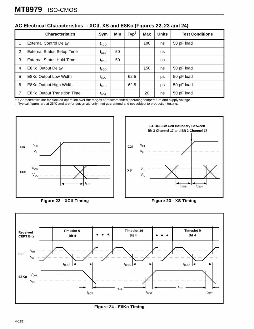
† Characteristics are for clocked operation over the ranges of recommended operating temperature and supply voltage.‡ Typical figures are at 25°C and are for design aid only: not guaranteed and not subject to production testing.
AC Electrical Characteristics † - XCtl, XS and E8Ko (Figures 22, 23 and 24)
Characteristics Sym Min Typ ‡ Max Units Test Conditions
1 External Control Delay tXCD 100 ns 50 pF load
2 External Status Setup Time tXSS 50 ns
3 External Status Hold Time tXSH 50 ns
4 E8Ko Output Delay t8OD 150 ns 50 pF load
5 E8Ko Output Low Width t8OL 62.5 µs 50 pF load
6 E8Ko Output High Width t8OH 62.5 µs 50 pF load
7 E8Ko Output Transition Time t8OT 20 ns 50 pF load
Figure 22 - XCtl Timing
F0i
XCtl
tXCD
VIH
VIL
VOH
VOL
Figure 23 - XS Timing
ST-BUS Bit Cell Boundary BetweenBit 3 Channel 17 and Bit 2 Channel 17
tXSS tXSH
C2i
XS
VIH
VIL
VIH
VIL
Figure 24 - E8Ko Timing
Timeslot 0
Bit 4
Timeslot 16Bit 4
Timeslot 0Bit 4
Received CEPT Bits
E2iVIH
VIL
E8KoVOH
VOL
t8OD
t8OT
t8OD t8OD
• • • • • •
t8OL t8OH
t8OT t8OT
ISO-CMOS MT8979
4-183
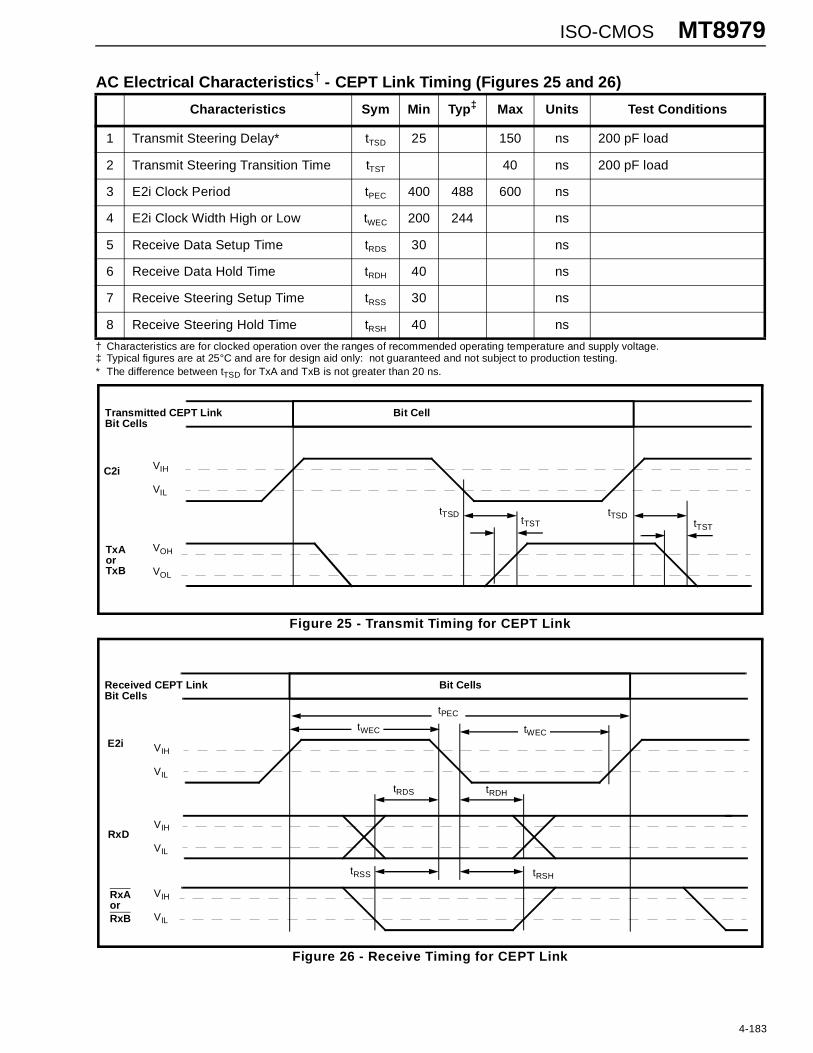
† Characteristics are for clocked operation over the ranges of recommended operating temperature and supply voltage.‡ Typical figures are at 25°C and are for design aid only: not guaranteed and not subject to production testing.* The difference between tTSD for TxA and TxB is not greater than 20 ns.
Figure 25 - Transmit Timing for CEPT Link
Figure 26 - Receive Timing for CEPT Link
AC Electrical Characteristics † - CEPT Link Timing (Figures 25 and 26)
Characteristics Sym Min Typ ‡ Max Units Test Conditions
1 Transmit Steering Delay* tTSD 25 150 ns 200 pF load
2 Transmit Steering Transition Time tTST 40 ns 200 pF load
3 E2i Clock Period tPEC 400 488 600 ns
4 E2i Clock Width High or Low tWEC 200 244 ns
5 Receive Data Setup Time tRDS 30 ns
6 Receive Data Hold Time tRDH 40 ns
7 Receive Steering Setup Time tRSS 30 ns
8 Receive Steering Hold Time tRSH 40 ns
Transmitted CEPT LinkBit Cells
C2i
TxAorTxB
VIH
VIL
VOH
VOL
tTSTtTSD
tTST
tTSD
Bit Cell
Bit CellsReceived CEPT LinkBit Cells
E2i
RxAorRxB
VIH
VIL
VIH
VIL
VIH
VIL
tWEC tWEC
tRDS tRDH
tRSS tRSH
RxD
tPEC

MT8979 ISO-CMOS
4-184
AppendixControl and Status Register Summary
Master Control Word 1 (MCW1) - CSTi0, Channel 15
Master Control Word 2 (MCW2) - CSTi0, Channel 31
Master Control Word 3 (MCW3) - CSTi1, Channel 18
Per Channel Cotnrol Word - CSTi0, Channels 0-14 and 16-30
Channel Associated Signalling - CSTi1, Channels N = 1 to 15
Frame Alignment Signals - CSTi1, Channel 16
Multiframe Alignment Signals - CSTi1, Channel 0
Non-Frame Alignment Signal - CSTi1, Channel 17
7 6 5 4 3 2 1 0
UNUSED
Keep at 1
LOOP16 1 Enabled0 Disabled
UNUSED
Keep at 1
NDBD
1 No Debounce
0 Debounce
NDBC
1 No Debounce
0 Debounce
NDBB
1 No Debounce
0 Debounce
NDBA
1 No Debounce
0 Debounce
UNUSED
Keep at 1
UNUSED
Keep at 0
CCS
1 CommonChannel
0 ChannelAssociated
8 kHz SEL
1 Enabled
0 Disabled
TXAIS
1 Alarm On
0 Alarm Off
TXTS16AIS
1 Alarm On
0 Alarm Off
XCTL
1 Set High
0 Cleared
UNUSED
UNUSED
Keep at 0
SiMUX
1 Enabled0 Disabled
RMLOOP
1 Enabled
0 Disabled
HDB3en
1 Disabled
0 Enabled
Maint
1 Enabled
0 Disabled
CRCen
1 Enabled
0 Disabled
DGLOOP
1 Enabled
0 Disabled
ReFRDevice
reframes onHigh to LowTransition
DATA
1 No ADI
0 Enable ADI
LOOP
1 Enabled0 Disabled
RxPAD4 RxPAD2 RxPAD1 TxPAD4 TxPAD2 TxPAD1
A(N)
TxSignalling Bit
B(N)
TxSignalling Bit
C(N)
TxSignalling Bit
D(N)
TxSignalling Bit
A(N + 15)
TxSignalling Bit
B(N + 15)
TxSignalling Bit
C(N + 15)
TxSignalling Bit
D(N + 15)
TxSignalling Bit
IUO
Should bekept at 1
FAF2-8
Frame Alignment Signal - Keep at "0011011"
MA1-4
Multiframe Alignment Signal - Keep at "0000"
X1
Spare BitShould be 1
Y
1 Alarm On
0 Alarm Off
X2, X3
Spare Bits - Should be 1
IU1
Reserved forInternational
Use
NFAF
Keep at "1"
ALM
1 Alarm On
0 Alarm Off
NU1-5
Bits Reserved for National Use - Should be kept at "1"

ISO-CMOS MT8979
4-185
Master Control Word 1 (MSW1) - CSTo, Channel 18
Master Status Word 2 (MSW2) - CSTo, Channel 21
Phase Status Word - CSTo, Channel 19
CRC Error Counter - CSTo, Channel 20
Received Channel Associated Signalling - CSTo, Channels N = 1 to 15
Received Frame Alignment Signals - CSTo, Channel 16
Received Multiframe Alignment Signals - CSTo, Channel 0
Received Non-Frame Alignment Signal - CSTo, Channel 17
7 6 5 4 3 2 1 0
TFSYN
1 Out of Sync
0 In Sync
MFSYN
1 Out of Sync
0 In Sync
ERR
FrameAlignment
Signal ErrorCount
SLIP
ChangesState when
SlipPerformed
RXAIS
1 Alarm Detected0 No Alarm
TXTS16AIS
1 Alarm Detected0 No Alarm
XS
1 XSt High
0 XSt Low
UNUSED
Si2Remote SMF2
is:
1 Correct
0 Errored
Si1Remote SMF1
is:
1 Correct
0 Errored
UNUSED CRC TimerTransitionfrom 1 to 0
indicates startof CRC Error
Counter
CRC Ref
1 Reframedforced by lackof CRC frame
CRC Sync
1 CRC Framenot Detected0 CRC FrameDetected
FrmPhase
Bit 8 of PhaseStatus Word
TxTSC
Transmit Timeslot Count, Timeslots between F0i and E8Ko
TxBTC
Transmit Bit Count - bit positions within TxTSCbetween F0i and E8Ko
CERC 0 - 7
Bits 0 - 7 of CRC Error Counter
A(N)
RxSignalling Bit
B(N)
RxSignalling Bit
C(N)
RxSignalling Bit
D(N)
RxSignalling Bit
A(N + 15)
RxSignalling Bit
B(N + 15)
RxSignalling Bit
C(N + 15)
RxSignalling Bit
D(N + 15)
RxSignalling Bit
IUO
InternationalBit
FAF2-8
Received Frame Alignment Signal
MA1-4
Received Multiframe Alignment Signal
X1
InternationalBit
Y
1 Remote MF Lost0 Remote MF Detected
X2, X3
International Bits
IU1
Reserved forInternational
Use
NFAF ALM
1 Detected
0 Not Detected
NU1-5
Received Bits Reserved for National Use

MT8979 ISO-CMOS
4-186
NOTES: