iso8200bq - st.com · this is information on a product in full production. may 2018 docid027303 rev...
TRANSCRIPT

This is information on a product in full production.
April 2019 DocID027303 Rev 7 1/39
ISO8200BQ
Galvanic isolated octal high-side smart power solid state-relay
Datasheet - production data
Features Vdemag = VCC - 45 V (per channel) RDS(on) = 0.11 (per channel) IOUT = 0.7 A (per channel) VCC = 45 V Parallel input interface Direct and synchronous control mode High common mode transient immunity Short-circuit protection Channel overtemperature protection Thermal independence of separate channels Common output disable pin Case overtemperature protection Loss of GNDCC and VCC protection Undervoltage shutdown with auto-restart and
hysteresis Overvoltage protection (VCC clamping) Very low supply current Common fault open-drain output 5 V and 3.3 V TTL/CMOS compatible I/Os Fast demagnetization of inductive loads Reset function for IC output disable ESD protection Designed to meet IEC 61000-4-2, IEC 61000-
4-4, IEC 61000-4-5 and IEC 61000-4-8 UL1577 and UL508 certified Safety Limits as per VDE0884-11
Applications Programmable logic control Industrial PC peripheral input/output Numerical control machines Drivers for all types of loads (resistive,
capacitive, inductive)
DescriptionThe ISO8200BQ is a galvanic isolated 8-channel driver featuring a very low supply current. It contains 2 independent galvanic isolated voltage domains (VCC for the power stage and VDD for the digital stage). Additional embedded functions are: loss of GND protection, undervoltage shutdown with hysteresis, and reset function for immediate power output shutdown.
IC is intended to drive any kind of load with one side connected to ground. Active channel current limitation combined with thermal shutdown, (independent for each channel), and automatic restart, protect the device against overload and short-circuit. In overload conditions, if junction temperature overtakes threshold, the channel involved is turned off and on again automatically after the IC temperature decreases below a reset threshold. If this condition causes case temperature to reach TCR limit threshold, the overloaded channel is turned off and it only restarts when case and junction temperature decrease down to the reset thresholds. Non- overloaded channels continue operating normally. An internal circuit provides an OR-wired non-latched common FAULT indicator signaling the channel OVT. The FAULT pin is an open-drain active low fault indication pin.
TFQFPN32
www.st.com
Contents ISO8200BQ
2/39 DocID027303 Rev 7
Contents
1 Block diagram . . . . . . . . . . . . . . . . . . . . . . . . . . . . . . . . . . . . . . . . . . . . . . 6
2 Pin connection . . . . . . . . . . . . . . . . . . . . . . . . . . . . . . . . . . . . . . . . . . . . . . 7
3 Absolute maximum ratings . . . . . . . . . . . . . . . . . . . . . . . . . . . . . . . . . . . 9
4 Thermal data . . . . . . . . . . . . . . . . . . . . . . . . . . . . . . . . . . . . . . . . . . . . . . . 9
5 Electrical characteristics . . . . . . . . . . . . . . . . . . . . . . . . . . . . . . . . . . . . 10
6 Functional description . . . . . . . . . . . . . . . . . . . . . . . . . . . . . . . . . . . . . . 176.1 Parallel interface . . . . . . . . . . . . . . . . . . . . . . . . . . . . . . . . . . . . . . . . . . . . 17
6.1.1 Input signals (IN1 to IN8) . . . . . . . . . . . . . . . . . . . . . . . . . . . . . . . . . . . . 176.1.2 Load input data (LOAD) . . . . . . . . . . . . . . . . . . . . . . . . . . . . . . . . . . . . . 176.1.3 Output synchronization (SYNC) . . . . . . . . . . . . . . . . . . . . . . . . . . . . . . . 176.1.4 Watchdog . . . . . . . . . . . . . . . . . . . . . . . . . . . . . . . . . . . . . . . . . . . . . . . . 186.1.5 Output enable (OUT_EN) . . . . . . . . . . . . . . . . . . . . . . . . . . . . . . . . . . . 19
6.2 Direct control mode (DCM) . . . . . . . . . . . . . . . . . . . . . . . . . . . . . . . . . . . . 19
6.3 Synchronous control mode (SCM) . . . . . . . . . . . . . . . . . . . . . . . . . . . . . . 21
6.4 Fault indication . . . . . . . . . . . . . . . . . . . . . . . . . . . . . . . . . . . . . . . . . . . . . 236.4.1 Junction overtemperature and case overtemperature . . . . . . . . . . . . . . 23
7 Power section . . . . . . . . . . . . . . . . . . . . . . . . . . . . . . . . . . . . . . . . . . . . . 257.1 Current limitation . . . . . . . . . . . . . . . . . . . . . . . . . . . . . . . . . . . . . . . . . . . 25
7.2 Thermal protection . . . . . . . . . . . . . . . . . . . . . . . . . . . . . . . . . . . . . . . . . . 26
8 Reverse polarity protection . . . . . . . . . . . . . . . . . . . . . . . . . . . . . . . . . . 28
9 Reverse polarity on VDD . . . . . . . . . . . . . . . . . . . . . . . . . . . . . . . . . . . . 30
10 Demagnetization energy . . . . . . . . . . . . . . . . . . . . . . . . . . . . . . . . . . . . . 31
11 Conventions . . . . . . . . . . . . . . . . . . . . . . . . . . . . . . . . . . . . . . . . . . . . . . . 31Supply voltage and power output conventions . . . . . . . . . . . . . . . . . . . . . . . . . . . 31

DocID027303 Rev 7 3/39
ISO8200BQ Contents
39
12 Thermal information . . . . . . . . . . . . . . . . . . . . . . . . . . . . . . . . . . . . . . . . 32Thermal impedance . . . . . . . . . . . . . . . . . . . . . . . . . . . . . . . . . . . . . . . . . . . . . . . 32
13 Package information . . . . . . . . . . . . . . . . . . . . . . . . . . . . . . . . . . . . . . . . 3313.1 TFQFPN32 package information . . . . . . . . . . . . . . . . . . . . . . . . . . . . . . . 33
14 Packing information . . . . . . . . . . . . . . . . . . . . . . . . . . . . . . . . . . . . . . . . 3614.1 TFQFPN32 packing information . . . . . . . . . . . . . . . . . . . . . . . . . . . . . . . . 36
14.1.1 TFQFPN32 packing method concept . . . . . . . . . . . . . . . . . . . . . . . . . . . 3614.1.2 TFQFPN32 winding direction . . . . . . . . . . . . . . . . . . . . . . . . . . . . . . . . . 3814.1.3 TFQFPN32 leader and trailer . . . . . . . . . . . . . . . . . . . . . . . . . . . . . . . . . 38
15 Ordering information . . . . . . . . . . . . . . . . . . . . . . . . . . . . . . . . . . . . . . . 39
16 Revision history . . . . . . . . . . . . . . . . . . . . . . . . . . . . . . . . . . . . . . . . . . . 39

List of tables ISO8200BQ
4/39 DocID027303 Rev 7
List of tables
Table 1. Pin description . . . . . . . . . . . . . . . . . . . . . . . . . . . . . . . . . . . . . . . . . . . . . . . . . . . . . . . . . . . 7Table 2. Absolute maximum ratings . . . . . . . . . . . . . . . . . . . . . . . . . . . . . . . . . . . . . . . . . . . . . . . . . . 9Table 3. Thermal data. . . . . . . . . . . . . . . . . . . . . . . . . . . . . . . . . . . . . . . . . . . . . . . . . . . . . . . . . . . . . 9Table 4. Power section . . . . . . . . . . . . . . . . . . . . . . . . . . . . . . . . . . . . . . . . . . . . . . . . . . . . . . . . . . . 10Table 5. Digital supply voltage . . . . . . . . . . . . . . . . . . . . . . . . . . . . . . . . . . . . . . . . . . . . . . . . . . . . . 10Table 6. Diagnostic pin and output protection function. . . . . . . . . . . . . . . . . . . . . . . . . . . . . . . . . . . 11Table 7. Power switching characteristics (VCC = 24 V; -40 °C < TJ < 125 °C) . . . . . . . . . . . . . . . . 11Table 8. Logic input and output . . . . . . . . . . . . . . . . . . . . . . . . . . . . . . . . . . . . . . . . . . . . . . . . . . . . 14Table 9. Parallel interface timings (VDD = 5 V; VCC= 24 V; -40 °C < TJ < 125 °C). . . . . . . . . . . . . 14Table 10. Insulation and safety-related specifications . . . . . . . . . . . . . . . . . . . . . . . . . . . . . . . . . . . . 15Table 11. IEC 60747-5-2 insulation characteristics . . . . . . . . . . . . . . . . . . . . . . . . . . . . . . . . . . . . . . 15Table 12. Safety limits. . . . . . . . . . . . . . . . . . . . . . . . . . . . . . . . . . . . . . . . . . . . . . . . . . . . . . . . . . . . . 16Table 13. Interface signal operation (general) . . . . . . . . . . . . . . . . . . . . . . . . . . . . . . . . . . . . . . . . . . 17Table 14. Interface signal operation in direct control mode . . . . . . . . . . . . . . . . . . . . . . . . . . . . . . . . 19Table 15. Interface signal operation in synchronous control mode. . . . . . . . . . . . . . . . . . . . . . . . . . . 21Table 16. TFQFPN32 package mechanical data . . . . . . . . . . . . . . . . . . . . . . . . . . . . . . . . . . . . . . . . 35Table 17. Ordering information . . . . . . . . . . . . . . . . . . . . . . . . . . . . . . . . . . . . . . . . . . . . . . . . . . . . . . 39Table 18. Document revision history. . . . . . . . . . . . . . . . . . . . . . . . . . . . . . . . . . . . . . . . . . . . . . . . . . 39
DocID027303 Rev 7 5/39
ISO8200BQ List of figures
39
List of figures
Figure 1. Block diagram . . . . . . . . . . . . . . . . . . . . . . . . . . . . . . . . . . . . . . . . . . . . . . . . . . . . . . . . . . . . 6Figure 2. Pin connection (top through view). . . . . . . . . . . . . . . . . . . . . . . . . . . . . . . . . . . . . . . . . . . . . 7Figure 3. RDS(on) measurement . . . . . . . . . . . . . . . . . . . . . . . . . . . . . . . . . . . . . . . . . . . . . . . . . . . . 12Figure 4. dV/dT . . . . . . . . . . . . . . . . . . . . . . . . . . . . . . . . . . . . . . . . . . . . . . . . . . . . . . . . . . . . . . . . . 12Figure 5. td(ON) - td(OFF) synchronous mode . . . . . . . . . . . . . . . . . . . . . . . . . . . . . . . . . . . . . . . . . 13Figure 6. td(ON) - td(OFF) direct control mode . . . . . . . . . . . . . . . . . . . . . . . . . . . . . . . . . . . . . . . . . 13Figure 7. Watchdog behavior . . . . . . . . . . . . . . . . . . . . . . . . . . . . . . . . . . . . . . . . . . . . . . . . . . . . . . . 18Figure 8. Output channel enable timing . . . . . . . . . . . . . . . . . . . . . . . . . . . . . . . . . . . . . . . . . . . . . . . 19Figure 9. Direct control mode IC configuration. . . . . . . . . . . . . . . . . . . . . . . . . . . . . . . . . . . . . . . . . . 20Figure 10. Direct control mode time diagram. . . . . . . . . . . . . . . . . . . . . . . . . . . . . . . . . . . . . . . . . . . . 20Figure 11. Synchronous control mode IC configuration. . . . . . . . . . . . . . . . . . . . . . . . . . . . . . . . . . . . 21Figure 12. Synchronous control mode time diagram . . . . . . . . . . . . . . . . . . . . . . . . . . . . . . . . . . . . . . 22Figure 13. Multiple device synchronous control mode. . . . . . . . . . . . . . . . . . . . . . . . . . . . . . . . . . . . . 22Figure 14. Thermal status update (DCM). . . . . . . . . . . . . . . . . . . . . . . . . . . . . . . . . . . . . . . . . . . . . . . 23Figure 15. Thermal status update (SCM). . . . . . . . . . . . . . . . . . . . . . . . . . . . . . . . . . . . . . . . . . . . . . . 24Figure 16. Current limitation with different load conditions . . . . . . . . . . . . . . . . . . . . . . . . . . . . . . . . . 25Figure 17. Thermal protection flowchart. . . . . . . . . . . . . . . . . . . . . . . . . . . . . . . . . . . . . . . . . . . . . . . . 26Figure 18. Thermal protection . . . . . . . . . . . . . . . . . . . . . . . . . . . . . . . . . . . . . . . . . . . . . . . . . . . . . . . 27Figure 19. Reverse polarity protection . . . . . . . . . . . . . . . . . . . . . . . . . . . . . . . . . . . . . . . . . . . . . . . . . 28Figure 20. Reverse polarity protection on VDD . . . . . . . . . . . . . . . . . . . . . . . . . . . . . . . . . . . . . . . . . . 29Figure 21. Maximum demagnetization energy vs. load current, typical values Tamb = 125 °C . . . . . 30Figure 22. Supply voltage and power output conventions . . . . . . . . . . . . . . . . . . . . . . . . . . . . . . . . . . 30Figure 23. Simplified thermal model. . . . . . . . . . . . . . . . . . . . . . . . . . . . . . . . . . . . . . . . . . . . . . . . . . . 31Figure 24. TFQFPN32 package outline . . . . . . . . . . . . . . . . . . . . . . . . . . . . . . . . . . . . . . . . . . . . . . . . 32Figure 25. TFQFPN32 package detail outline . . . . . . . . . . . . . . . . . . . . . . . . . . . . . . . . . . . . . . . . . . . 33Figure 26. TFQFPN32 suggested footprint (measured in mm) . . . . . . . . . . . . . . . . . . . . . . . . . . . . . . 33Figure 27. TFQFPN32 packing method concept . . . . . . . . . . . . . . . . . . . . . . . . . . . . . . . . . . . . . . . . . 35Figure 28. TFQFPN32 carrier tape . . . . . . . . . . . . . . . . . . . . . . . . . . . . . . . . . . . . . . . . . . . . . . . . . . . 36Figure 29. TFQFPN32 reel. . . . . . . . . . . . . . . . . . . . . . . . . . . . . . . . . . . . . . . . . . . . . . . . . . . . . . . . . . 36Figure 30. TFQFPN32 winding direction . . . . . . . . . . . . . . . . . . . . . . . . . . . . . . . . . . . . . . . . . . . . . . . 37Figure 31. TFQFPN32 leader and trailer . . . . . . . . . . . . . . . . . . . . . . . . . . . . . . . . . . . . . . . . . . . . . . . 37

Block diagram ISO8200BQ
6/39 DocID027303 Rev 7
1 Block diagram
Figure 1. Block diagram
DocID027303 Rev 7 7/39
ISO8200BQ Pin connection
39
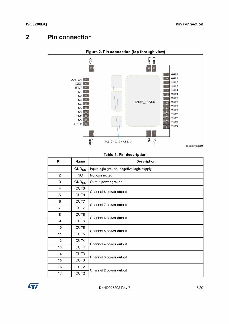
2 Pin connection
Figure 2. Pin connection (top through view)
Table 1. Pin description Pin Name Description
1 GNDDD Input logic ground, negative logic supply
2 NC Not connected
3 GNDCC Output power ground
4 OUT8Channel 8 power output
5 OUT8
6 OUT7Channel 7 power output
7 OUT7
8 OUT6Channel 6 power output
9 OUT6
10 OUT5Channel 5 power output
11 OUT5
12 OUT4Channel 4 power output
13 OUT4
14 OUT3Channel 3 power output
15 OUT3
16 OUT2Channel 2 power output
17 OUT2

Pin connection ISO8200BQ
8/39 DocID027303 Rev 7
18 OUT1Channel 1 power output
19 OUT1
20 VDD Positive logic supply
21 OUT_EN Output enable
22 SYNC Input-to-output synchronization signal. Active low, see Section 6.3: Synchronous control mode (SCM) on page 21.
23 LOAD Load input data signal. Active low, see Section 6.3
24 IN1 Channel 1 input
25 IN2 Channel 2 input
26 IN3 Channel 3 input
27 IN4 Channel 4 input
28 IN5 Channel 5 input
29 IN6 Channel 6 input
30 IN7 Channel 7 input
31 IN8 Channel 8 input
32 FAULT Common fault indication, active low
TAB(VCC) VCC Exposed tab internally connected to VCC, positive power supply voltage
TAB(GNDCC) GNDCC Exposed tab internally connected to GNDCC
Table 1. Pin description (continued)Pin Name Description

DocID027303 Rev 7 9/39
ISO8200BQ Absolute maximum ratings
39
3 Absolute maximum ratings
4 Thermal data
Table 2. Absolute maximum ratingsSymbol Parameter Min. Max. Unit
VCC Power supply voltage -0.3 45 V
VDD Digital supply voltage -0.3 6.5 V
VIN DC input pin voltage (INx, OUT_EN, LOAD, SYNC) -0.3 +6.5 V
VFAULT Fault pin voltage -0.3 +6.5 V
IGNDDD DC digital ground reverse current - -25 mA
IOUT Channel output current (continuous) - Internally limited A
IGNDcc DC power ground reverse current - -250 mA
-IOUT Reverse output current (single channel) - -5 A
IIN DC input pin current (INx, OUT_EN, LOAD, SYNC) -10 + 10 mA
IFAULT Fault pin current -10 + 10 mA
VESDElectrostatic discharge with human body model (R = 1.5 k; C = 100 pF) - 2000 V
EAS
Single pulse avalanche energy per channel not simultaneously at Tamb= 125 °C, IOUT = 0.5 A - 1.8
JSingle pulse avalanche energy per channel, all channels driven simultaneously at Tamb = 125 °C, IOUT = 0.5 A - 0.35
PTOT Power dissipation at Tc = 25 °C - Internally limited(1)
1. Protection functions are intended to avoid IC damage in fault conditions and are not intended for continuous operation. Continuous or repetitive operations of protection functions may reduce the IC lifetime.
W
TJ Junction operating temperature - Internally limited(1) °C
TSTG Storage temperature - -55 to 150 °C
Table 3. Thermal dataSymbol Parameter Max. value Unit
Rthj-case Thermal resistance, junction-case((1)
1. For each channel.
2 °C/W
Rthj-amb Thermal resistance, junction-ambient(2)
2. TFQFPN32 mounted on the product evaluation board (FR4, 4 layers, 8 cm2 for each layer, copper thickness 35 mm).
15 °C/W

Electrical characteristics ISO8200BQ
10/39 DocID027303 Rev 7
5 Electrical characteristics
(10.5 V < VCC < 36 V; -40 °C < TJ < 125 °C, unless otherwise specified)
Table 4. Power sectionSymbol Parameter Test conditions Min. Typ. Max. Unit
VCC(THON)VCC undervoltage turn-ON threshold - - 9.5 10.5 V
VCC(THOFF)VCC undervoltage turn-OFF threshold - 8 9 - V
VCC(hys) VCC undervoltage hysteresis - 0.25 0.5 - V
VCCclamp Clamp on VCC pin Iclamp = 20 mA 45 50 52 V
RDS(on) On-state resistance(1)
1. See Figure 3: RDS(on) measurement.
IOUT = 0.5 A, TJ = 25 °CIOUT = 0.5 A TJ = 125 °C
-0.12
0.24
Rpd Output pull-down resistor - 210 - k
ICC Power supply currentAll channels in OFF-stateAll channels in ON-state
- 5 - mA
ILGNDGround disconnection output current
VCC = VGND = 0 V VOUT = -24 V
- - 500 μA
VOUT(OFF) Off-state output voltage Channel OFF and IOUT = 0 A - - 1 V
IOUT(OFF) Off-state output current Channel OFF and VOUT = 0 V - - 5 μA
Table 5. Digital supply voltageSymbol Parameter Test conditions Min. Typ. Max. Unit
VDD Operating voltage - 2.75 - 5.5 V
VDD(THON)VDD undervoltage turn-ON threshold - 2.55 - 2.75 V
VDD(THOFF)VDD undervoltage turn-OFF threshold - 2.45 - 2.65 V
VDD(hys) VDD undervoltage hysteresis - 0.04 0.1 - V
IDD IDD supply current
VDD = 5 V and input channel with a steady logic levelVDD = 3.3 V and input channel with a steady logic level
-
-
4.5
4.4
6
5.9
mA
mA

DocID027303 Rev 7 11/39
ISO8200BQ Electrical characteristics
39
Table 6. Diagnostic pin and output protection functionSymbol Parameter Test conditions Min. Typ. Max. Unit
VFAULTFAULT pin open-drain voltage output low IFAULT = 10 mA - - 0.4 V
ILFAULT FAULT output leakage current VFAULT = 5 V - - 1 μA
IPEAKMaximum DC output current before limitation
VCC = 24 V RLOAD = 0
- 1.6 - A
ILIM Short-circuit current limitation - 0.7 1.3 1.9 A
Hyst ILIM tracking limits - - 0.3 - A
TJSD Junction shutdown temperature - 150 170 - °C
TJR Junction reset temperature - - 150 - °C
THIST Junction thermal hysteresis - - 20 - °C
TCSD Case shutdown temperature - 115 130 145 °C
TCR Case reset temperature - - 110 - °C
TCHYST Case thermal hysteresis - - 20 - °C
Vdemag Output voltage at turn-OFFIOUT = 0.5 A ILOAD > = 1 mH
VCC -45 VCC -50 VCC -52 V
Table 7. Power switching characteristics (VCC = 24 V; -40 °C < TJ < 125 °C)Symbol Parameter Test conditions Min. Typ. Max. Unit
dV/dt(ON) Turn-ON voltage slope IOUT = 0.5 A, resistive load 48 - 5.6 - V/μs
dV/dt(OFF) Turn-OFF voltage slope IOUT = 0.5 A, resistive load 48 - 2.81 - V/μs
td(ON) Turn-ON delay time(1)
1. See Figure 3: RDS(on) measurement , Figure 4: dV/dT and Figure 6: td(ON) - td(OFF) direct control mode.
IOUT = 0.5 A, resistive load 48 - 17 22 μs
td(OFF) Turn-OFF delay time(1) IOUT = 0.5 A, resistive load 48 - 22 40 μs
tf Fall time(1) IOUT = 0.5 A, resistive load 48 - 5 - μs
tr Rise time(1) IOUT = 0.5 A, resistive load 48 - 5 - μs

Electrical characteristics ISO8200BQ
12/39 DocID027303 Rev 7
Figure 3. RDS(on) measurement
Figure 4. dV/dT

DocID027303 Rev 7 13/39
ISO8200BQ Electrical characteristics
39
Figure 5. td(ON) - td(OFF) synchronous mode
Figure 6. td(ON) - td(OFF) direct control mode

Electrical characteristics ISO8200BQ
14/39 DocID027303 Rev 7
Table 8. Logic input and outputSymbol Parameter Test conditions Min. Typ. Max. Unit
VILLogic input pin low level voltage (INx, OUT_EN, LOAD, SYNC) - -0.3 0.3 x VDD V
VIHLogic input pin high level voltage (INx, OUT_EN, LOAD, SYNC) - 0.7 x VDD VDD + 0.3 V
VI(HYST)Logic input hysteresis voltage (INx, OUT_EN, LOAD, SYNC) VDD = 5 V - 100 - mV
IINLogic input pin current (INx, OUT_EN, LOAD, SYNC) VIN = 5 V 10 - - μA
tWM Power side watchdog time - 272 320 400 μs
Table 9. Parallel interface timings (VDD = 5 V; VCC= 24 V; -40 °C < TJ < 125 °C)Symbol Parameter Test conditions Min. Typ. Max. Unit
tdis(SYNC) SYNC disable time Sync. control mode 10 - - μs
tdis(DCM) SYNC, LOAD disable time Direct control mode 80 - - ns
tw(SYNC) SYNC negative pulse width Sync. control mode 20 - 195 μs
tsu(LOAD) LOAD setup time Sync. control mode 80 - - ns
th(LOAD) LOAD hold time Sync. control mode 400 - - ns
tw(LOAD) LOAD pulse width Sync. control mode 240 - - ns
tsu(IN) Input setup time - 80 - - ns
th(IN) Input hold time - 10 - - ns
tw(IN) Input pulse widthSync. control mode 160 - - ns
Direct control mode 20 - - μs
tINLD IN to LOAD timeDirect control mode From IN variation to LOAD falling edge
80 - - ns
tLDIN LOAD to IN timeDirect control modeFrom LOAD falling edge to IN variation
400 - - ns
tw(OUT_EN) OUT_EN pulse width - 150 - - ns
tp(OUT_EN) OUT_EN propagation delay - - 22 40 μs
tjitter(SCM)Jitter on single channel
Sync. modeDirect mode
--
--
620
μstjitter(DCM)
frefresh Refresh delay - - 15 - kHz

DocID027303 Rev 7 15/39
ISO8200BQ Electrical characteristics
39
Table 10. Insulation and safety-related specificationsSymbol Parameter Test conditions Value Unit
CLR Clearance (minimum external air gap)
Measured from input terminals to output terminals, the shortest distance through air 3.3 mm
CPG Creepage (minimum external tracking)
Measured from input terminals to output terminals, the shortest distance path along body 3.3 mm
CTIComparative tracking index (tracking resistance) DIN IEC 112/VDE 0303 part 1 600 V
Isolation group Material group (DIN VDE 0110, 1/89, Table 1) I -
Table 11. IEC 60747-5-2 insulation characteristicsSymbol Parameter Test conditions Value Unit
VPR Input to output test voltage
Method a, type test, tm = 10 s partial discharge < 5 pC 1500 VPEAK
Method b, 100% production test, tm = 1 s partial discharge < 5 pC 1758 VPEAK
VIOTM Transient overvoltageType test tini = 60 s
4245 VPEAK
VIOSMMaximum surge insulation voltage Type test 4245 VPEAK
RIO Insulation resistance VIO = 500 V at ts >109
VISO Insulation withstand voltage 1 min. type test 2500/3536 Vrms/VPEAK
VISO test Insulation withstand test 1 s 100% production 3000/4245 Vrms/VPEAK

Electrical characteristics ISO8200BQ
16/39 DocID027303 Rev 7
Table 12. Safety limits
Note: The above limits are measured according to VDE 0884-11. Respecting above limits prevents potential damage potential damage to the isolation barrier upon failure on logic or process side circuitry. User can use these values to protect the IC and consequently guarantee the safety of the embedded isolation barrier. LOGIC(X) stands for "any pin of logic side". OUT(X) stands for "any of the 8 output pins of process side".
Parameter Description Test Condition Limit value Unit
Input safety, Logic side
Tsi Safety temperature of Logic side - 150 oC
Psi Safety power of Logic side
VDD ≤ 6.5V,VLOGIC(x) ≤ 6.5V,ILOGIC(x) ≤ 10mA,TJ ≤ Tsi
0.9 W
Output safety, Process side
Tso Safety temperature of Process side - 150 oC
Pso Safety power of Process sideVCC ≤ 36V,IOUT(x) ≤ 1.5A,TJ ≤ Tso
4.5 W

DocID027303 Rev 7 17/39
ISO8200BQ Functional description
39
6 Functional description
6.1 Parallel interfaceSmart parallel interface built-in ISO8200BQ offers three interfacing signals easily managed by a microcontroller.
The LOAD signal enables the input buffer storing the value of the channel inputs.
The SYNC signal copies the input buffer value into the transmission buffer and manages the synchronization between low voltage side and the channel outputs on the isolated side. The OUT_EN signal enables the channel outputs.
An internal refresh signal updates the configuration of the channel outputs with a frefresh frequency. This signal can be disabled forcing low the SYNC input when LOAD is high.
SYNC and LOAD pins can be in direct control mode (DCM) or synchronous control mode (SCM).
The operation of these two signals is described as follows:
6.1.1 Input signals (IN1 to IN8)Inputs from IN1 to IN8 are the driving signals of the corresponding OUT1 to OUT8 outputs. Data are direct loaded on related outputs if SYNC and LOAD inputs are low (DCM operation) or stored into input buffer when LOAD is low and SYNC is high.
6.1.2 Load input data (LOAD)The input is active low; it stores the data from IN1 to IN8 into the input buffer.
6.1.3 Output synchronization (SYNC)The input is active low; it enables the ISO8200BQ transmission buffer loading input buffer data and manages the transmission between the two isolated sides of the device.
Table 13. Interface signal operation (general)LOAD SYNC OUT_EN Device behavior
Don't care Don't care Low(1)
1. The outputs are turned off on OUT_EN falling edge and they are kept disabled as long as it is low.
The outputs are disabled (turned off)
High High High The outputs are left unchanged
Low High HighThe input buffer is enabled The outputs are left unchanged
High Low HighThe internal refresh signal is disabled The transmission buffer is updated The outputs are left unchanged
Low Low High The device operates in direct control mode as described in Section 6.2: Direct control mode (DCM)

Functional description ISO8200BQ
18/39 DocID027303 Rev 7
6.1.4 WatchdogThe isolated side of the device provides a watchdog function in order to guarantee a safe condition when VDD supply voltage is missing.
If the logic side does not update the output status within tWD, all outputs are disabled until a new update request is received.
The refresh signal is also considered a valid update signal, so the isolated side watchdog does not protect the system from a failure of the host controller (MCU freezing).
Figure 7. Watchdog behavior

DocID027303 Rev 7 19/39
ISO8200BQ Functional description
39
6.1.5 Output enable (OUT_EN)This pin provides a fast way to disable all outputs simultaneously. When the OUT_EN pin is driven low the outputs are disabled. To enable the output stage, the OUT_EN pin has to be raised. This timing execution is compatible with an external reset push, safety requirement, and allows, in a PLC system, the microcontroller polling to obtain all internal information during a reset procedure.
Figure 8. Output channel enable timing
6.2 Direct control mode (DCM)When SYNC and LOAD inputs are driven by the same signal, the device operates in direct control mode (DCM).
In DCM the SYNC / LOAD signal operates as an active low input enable: When the signal is high, the current output configuration is kept regardless the input
values When the signal is low, each channel input directly drives the respective output
This operation mode can also be set shorting both signals to the digital ground; in this case the channel outputs are always directly driven by the inputs except when OUT_EN is low (outputs disabled).
Table 14. Interface signal operation in direct control modeSYNC / LOAD OUT_EN Device behavior
Don't care Low (1)
1. The outputs are turned off on OUT_EN falling edge and they are kept disabled as long as it is low.
The outputs are disabled (turned off)
High High The outputs are left unchanged
Low High The channel inputs drive the outputs

Functional description ISO8200BQ
20/39 DocID027303 Rev 7
Figure 9. Direct control mode IC configuration
Figure 10. Direct control mode time diagram

DocID027303 Rev 7 21/39
ISO8200BQ Functional description
39
6.3 Synchronous control mode (SCM)When SYNC and LOAD inputs are independently driven, the device can operate in synchronous control mode (SCM). The SCM is used to reduce the jittering of the outputs and to drive all outputs of different devices at the same time.
In SCM the LOAD signal is forced low to update the input buffer while the SYNC signal is high. The LOAD signal is raised and the SYNC one is forced low for at least tSYNC(SCM). During this period, the internal refresh is disabled and any pending transmission between the low voltage and the isolated side is completed. When the SYNC signal is raised the channel output configuration is changed according to the one stored in the input.
If the tSYNC(SCM) limit is met, the maximum jitter of the channel outputs is tjitter(SCM).
If more devices share the same SYNC signal, all device outputs change simultaneously with a maximum jitter related to maximum delay and maximum jitter for single device.
Figure 11. Synchronous control mode IC configuration
Table 15. Interface signal operation in synchronous control modeLOAD SYNC OUT_EN Device behavior
Don't care Don't care Low(1)
1. The outputs are turned off on OUT_EN falling edge and they are kept disabled as long as it is low.
The outputs are disabled (turned off)
High High High The outputs are left unchanged
Low High High The input buffer is enabled. The outputs are left unchanged.
High Low High The internal refresh signal is disabled. The transmission buffer is updated. The outputs are left unchanged.
High Rising edge High The outputs are updated according to the current transmission
buffer value
Low Low High Should be avoided (DCM operation only)

Functional description ISO8200BQ
22/39 DocID027303 Rev 7
Figure 12. Synchronous control mode time diagram
Figure 13. Multiple device synchronous control mode

DocID027303 Rev 7 23/39
ISO8200BQ Functional description
39
6.4 Fault indicationThe FAULT pin is an active low open-drain output indicating fault conditions. This pin is active when at least one of the following conditions occurs: Junction overtemperature of one or more channels (TJ >TTJSD) Communication error
The communication error is intended as an internal data corruption event in the data transfer through isolation. In case of communication error the outputs are initially kept in the previous status and then reset (turned off) at the first communication error during data transfer of the refresh signal.
6.4.1 Junction overtemperature and case overtemperatureThe thermal status of the device is updated during each transmission sequence between the two isolated sides.
In SCM operation, when the LOAD signal is high and the SYNC one is low, the communication is disabled. In this case the thermal status of the device cannot be updated and the FAULT indication can be different from the current status.
In any case, the thermal protection of the channel outputs is always operative.
Figure 14. Thermal status update (DCM)

Functional description ISO8200BQ
24/39 DocID027303 Rev 7
Figure 15. Thermal status update (SCM)

DocID027303 Rev 7 25/39
ISO8200BQ Power section
39
7 Power section
7.1 Current limitationThe current limitation process is active when the current sense connected on the output stage measures a current value, which is higher than a fixed threshold.
When this condition is verified the gate voltage is modulated to avoid the increase of the output current over the limitation value.
Figure 16 shows typical output current waveforms with different load conditions.
Figure 16. Current limitation with different load conditions

Power section ISO8200BQ
26/39 DocID027303 Rev 7
7.2 Thermal protectionThe device is protected against overheating in case of overload conditions. During the driving period, if the output is overloaded, the device suffers two different thermal stresses, the former related to the junction, and the latter related to the case.
The two faults have different trigger thresholds: the junction protection threshold is higher than the case protection one; generally the first protection, that is active in thermal stress conditions, is the junction thermal shutdown. The output is turned off when the temperature is higher than the related threshold and turned back on when it goes below the reset threshold. This behavior continues until the fault on the output is present.
If the thermal protection is active and the temperature of the package increases over the fixed case protection threshold, the case protection is activated and the output is switched off and back on when the junction temperature of each channel in fault and case temperature is below the respective reset thresholds.
Figure 17 shows the thermal protection behavior, while Figure 18 reports typical temperature trends and output vs. input state.
Figure 17. Thermal protection flowchart

DocID027303 Rev 7 27/39
ISO8200BQ Power section
39
Figure 18. Thermal protection

Reverse polarity protection ISO8200BQ
28/39 DocID027303 Rev 7
8 Reverse polarity protection
Reverse polarity protection can be implemented on board using two different solutions:1. Placing a resistor (RGND) between IC GND pin and load GND2. Placing a diode in parallel to a resistor between IC GND pin and load GND
If option 1 is selected, the minimum resistance value has to be selected according to Equation 1:
Equation 1
RGND VCC/IGNDcc
where IGNDcc is the DC reverse ground pin current and can be found in Section 3: Absolute maximum ratings on page 9.
Power dissipated by RGND during reverse polarity situations is:
Equation 2
PD = (VCC)2/RGND
If option 2 is selected, the diode has to be chosen by taking into account VRRM > |VCC| and its power dissipation capability:
Equation 3
PD IS * VF
Note: In normal operation (no reverse polarity), there is a voltage drop (ΔV) between GND of the device and GND of the system. Using option 1, ΔV = Rgnd * Icc. Using option 2, ΔV = VF@(IF).
Figure 19. Reverse polarity protection
This schematic can be used with any type of load.

DocID027303 Rev 7 29/39
ISO8200BQ Reverse polarity on VDD
39
9 Reverse polarity on VDD
The reverse polarity on VDD can be implemented on board by placing a diode between GNDDD pin and GND digital ground.
The diode has to be chosen by taking into account VRRM > |VDD| and its power dissipation capability:
Equation 4
PD IDD * VF
Note: In normal operation (no reverse polarity), there is a voltage drop (ΔV = VF@(Idd)) between GNDDD of the device and digital ground of the system. In order to guarantee to proper triggering of the input signal, ΔV(max.) must result lower than VIH(MIN).
Figure 20. Reverse polarity protection on VDD
Demagnetization energy ISO8200BQ
30/39 DocID027303 Rev 7
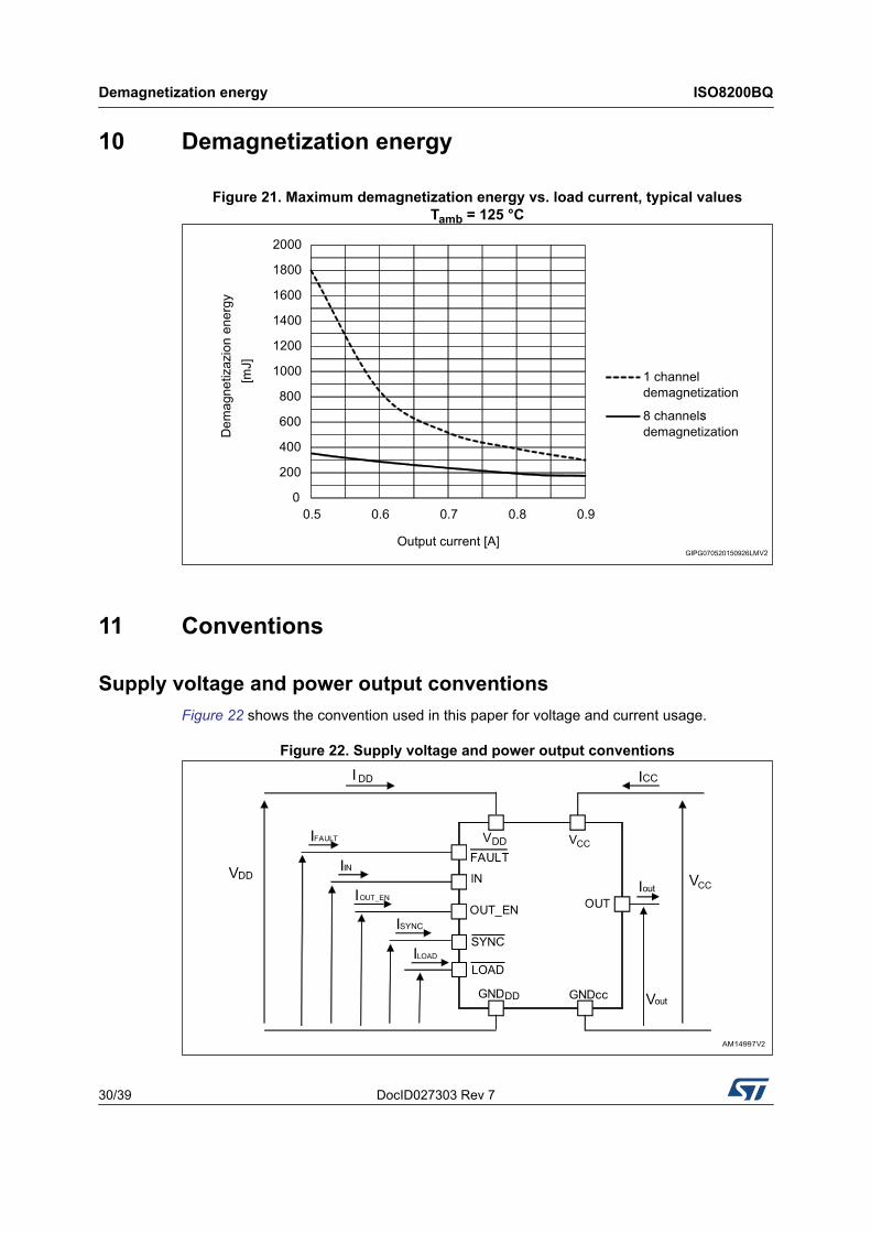
10 Demagnetization energy
Figure 21. Maximum demagnetization energy vs. load current, typical values Tamb = 125 °C
11 Conventions
Supply voltage and power output conventionsFigure 22 shows the convention used in this paper for voltage and current usage.
Figure 22. Supply voltage and power output conventions

DocID027303 Rev 7 31/39
ISO8200BQ Thermal information
39
12 Thermal information
Thermal impedance
Figure 23. Simplified thermal model
Package information ISO8200BQ
32/39 DocID027303 Rev 7
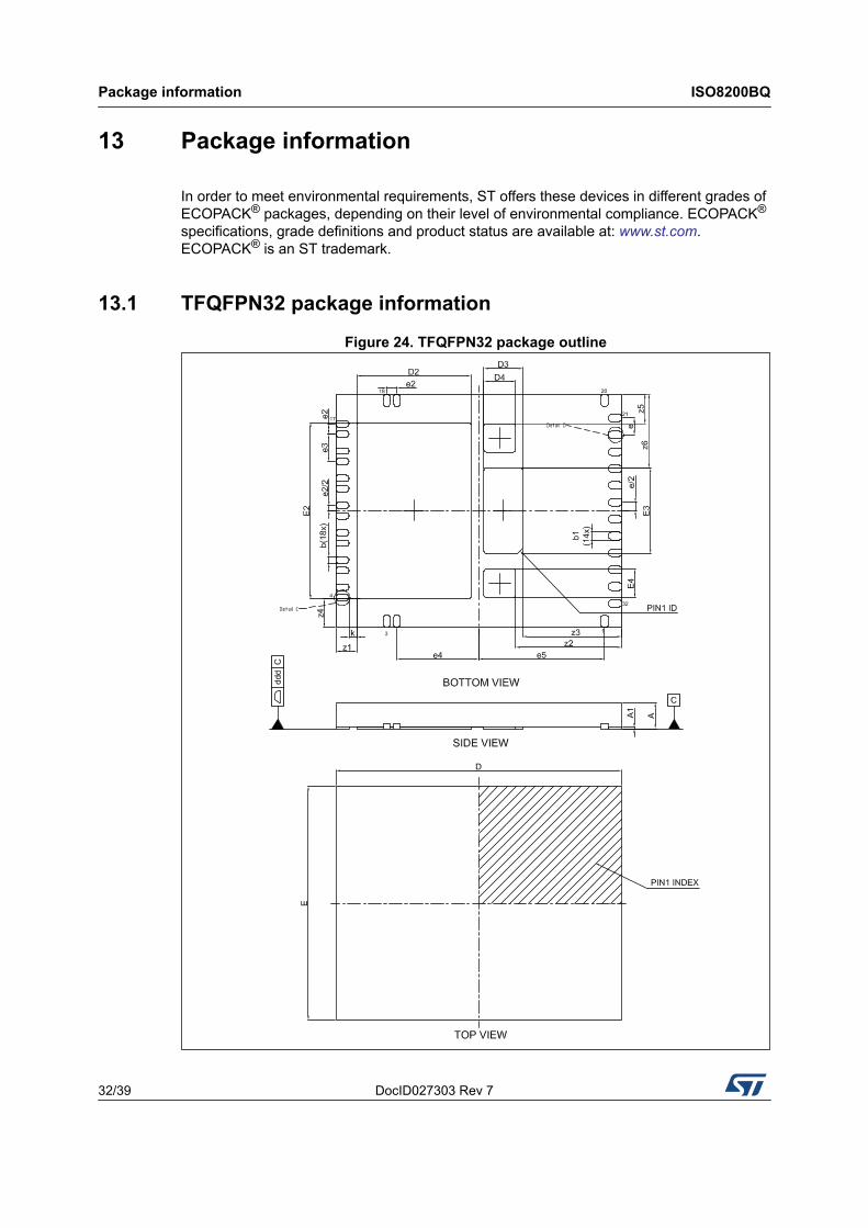
13 Package information
In order to meet environmental requirements, ST offers these devices in different grades of ECOPACK® packages, depending on their level of environmental compliance. ECOPACK® specifications, grade definitions and product status are available at: www.st.com. ECOPACK® is an ST trademark.
13.1 TFQFPN32 package information
Figure 24. TFQFPN32 package outline
DocID027303 Rev 7 33/39
ISO8200BQ Package information
39
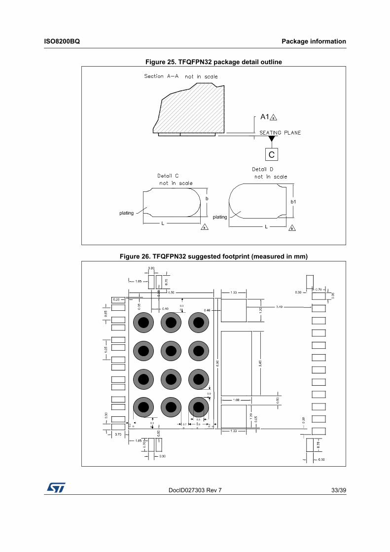
Figure 25. TFQFPN32 package detail outline
Figure 26. TFQFPN32 suggested footprint (measured in mm)
0.30 00.90 0.7
0 0.2
0 0.2
0 0.30
0.30
0.90

Package information ISO8200BQ
34/39 DocID027303 Rev 7
Table 16. TFQFPN32 package mechanical data
SymbolDimensions (mm]
Min. Typ. Max.
A 0.95 1.00 1.05
A1 0 - 0.05
b(1)
1. Dimensions “b” and “L” are measured on terminal plating surface.
0.20 0.25 0.30
b1(1) 0.25 0.30 0.35
D 10.90 11.0 11.10
E(1) 8.90 9.00 9.10
D2 4.30 4.40 4.50
E2 6.70 6.80 6.90
D3 1.40 1.50 1.60
E3 3.20 3.30 3.40
D4 1.13 1.23 1.33
E4 1.00 1.10 1.20
e - 0.65 -
e2 - 0.40 -
e3 - 1.05 -
e4 - 3.15 -
e5 - 4.85 -
k 0 0.30 -
z1 - 0.80 -
z2 - 4.07 -
z3 - 3.80 -
z4 - 1.10 -
z5 - 1.15 -
z6 - 2.85 -
L(1) 0.45 0.50 0.55

DocID027303 Rev 7 35/39
ISO8200BQ Packing information
39
14 Packing information
14.1 TFQFPN32 packing information
14.1.1 TFQFPN32 packing method concept
Figure 27. TFQFPN32 packing method concept

Packing information ISO8200BQ
36/39 DocID027303 Rev 7
Figure 28. TFQFPN32 carrier tape
Reel – 330 mm diameter x 101 mm hub x 24 mm width
Figure 29. TFQFPN32 reel

DocID027303 Rev 7 37/39
ISO8200BQ Packing information
39
14.1.2 TFQFPN32 winding direction
Figure 30. TFQFPN32 winding direction
14.1.3 TFQFPN32 leader and trailer
Figure 31. TFQFPN32 leader and trailer
Note: Leader and trailer length as per EAI-481specification.

Ordering information ISO8200BQ
38/39 DocID027303 Rev 7
15 Ordering information
16 Revision history
Table 17. Ordering informationOrder code Package Packing
ISO8200BQ TFQFPN32 Tube
ISO8200BQTR TFQFPN32 Tape and reel
Table 18. Document revision historyDate Revision Changes
17-Nov-2016 3 Datasheet promoted from preliminary to production data. Updated Table 6: Diagnostic pin and output protection function.
21-Apr-2017 4 Updated Table 10: “Insulation and safety-related specifications”. Minor text changes.
05-Oct-2017 5 Updated Table 11: “IEC 60747-5-2 insulation characteristics”.
18-May-2018 6
Updated Section : Features on page 1.Replaced Vdd by VDD in whole document.Updated titles of Table 7 on page 11 and Table 9 on page 14 .Updated titles of Figure 3 on page 12, Figure 5 on page 13, Figure 6 on page 13, Figure 20 on page 29 and Figure 21 on page 30 .Added cross-reference to Section 6.2 in Table 13 on page 17.Updated Figure 9 on page 20 and Figure 11 on page 21 (replaced ISO8200B by ISO8200BQ).Added Section 14 on page 35.Minor modifications throughout document.
24-Apr-2019 7
Added Table 12: Safety limits on page 15, Updated Table 2: Absolute maximum ratings on page 9 Updated Section : Features on page 1.Minor text changes.
DocID027303 Rev 7 39/39
ISO8200BQ
39
IMPORTANT NOTICE – PLEASE READ CAREFULLY
STMicroelectronics NV and its subsidiaries (“ST”) reserve the right to make changes, corrections, enhancements, modifications, and improvements to ST products and/or to this document at any time without notice. Purchasers should obtain the latest relevant information on ST products before placing orders. ST products are sold pursuant to ST’s terms and conditions of sale in place at the time of order acknowledgement.
Purchasers are solely responsible for the choice, selection, and use of ST products and ST assumes no liability for application assistance or the design of Purchasers’ products.
No license, express or implied, to any intellectual property right is granted by ST herein.
Resale of ST products with provisions different from the information set forth herein shall void any warranty granted by ST for such product.
ST and the ST logo are trademarks of ST. All other product or service names are the property of their respective owners.
Information in this document supersedes and replaces information previously supplied in any prior versions of this document.
© 2019 STMicroelectronics – All rights reserved