isolated igbt gate-drive fly-buck™ power supply with 4 … · 2014-08-05 · 2 isolated igbt...
TRANSCRIPT
An IMPORTANT NOTICE at the end of this TI reference design addresses authorized use, intellectual property matters and other important disclaimers and information.
All trademarks are the property of their respective owners.
TIDA00174-July 2014 Isolated IGBT Gate-Drive Fly-Buck™ Power Supply with 4 Outputs 1 Copyright © 2014, Texas Instruments Incorporated
TI Designs
Isolated IGBT Gate-Drive Fly-Buck™ Power Supply with 4 Outputs
TI Designs Design Features
TI Designs provide the foundation that you need including methodology, testing, and design files to quickly evaluate and customize the system. TI Designs help you accelerate your time to market. Design Resources
TIDA-00174 Tools Folder with Design Files LM5017 Product Folder C2000 HV Inverter Kit Development Kit Folder
Ask Our Analog Experts WEBENCH® Design Center
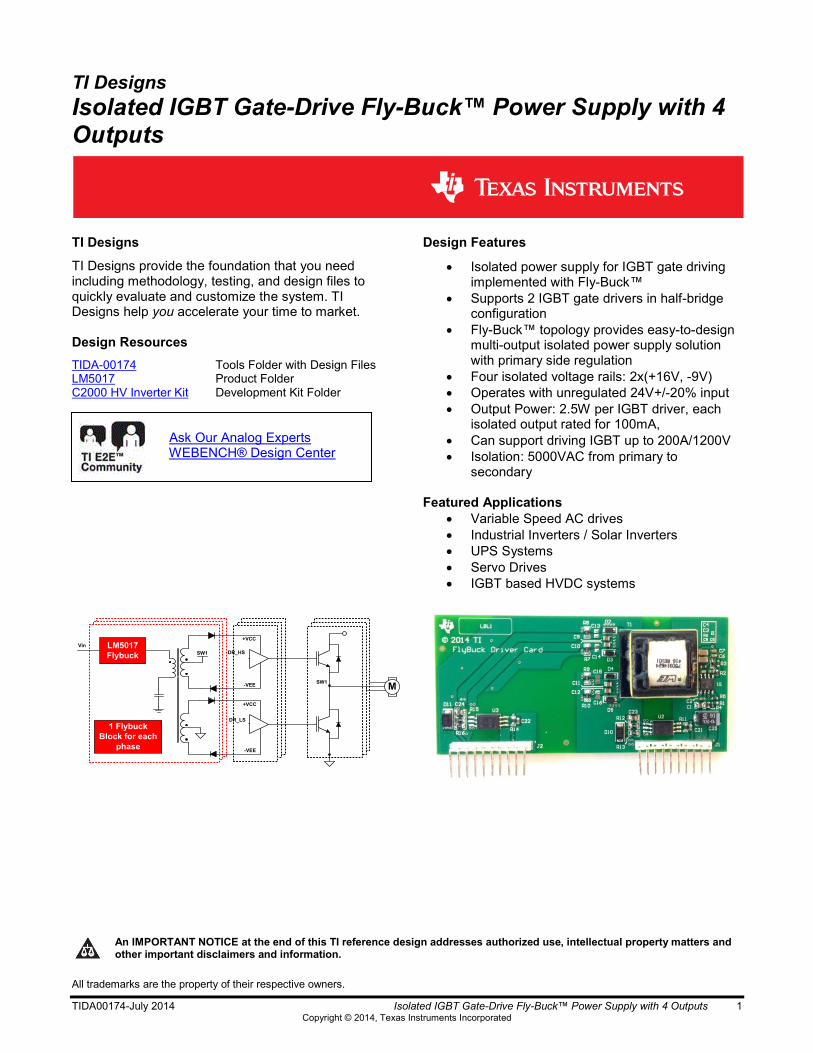
Isolated power supply for IGBT gate driving implemented with Fly-Buck™
Supports 2 IGBT gate drivers in half-bridge configuration
Fly-Buck™ topology provides easy-to-design multi-output isolated power supply solution with primary side regulation
Four isolated voltage rails: 2x(+16V, -9V)
Operates with unregulated 24V+/-20% input
Output Power: 2.5W per IGBT driver, each isolated output rated for 100mA,
Can support driving IGBT up to 200A/1200V
Isolation: 5000VAC from primary to secondary
Featured Applications
Variable Speed AC drives
Industrial Inverters / Solar Inverters
UPS Systems
Servo Drives
IGBT based HVDC systems
LM5017
Flybuck SW1
SW1M
DR_HS
DR_LS
-VEE
+VCC
-VEE
+VCC
Vin
1 Flybuck
Block for each
phase

www.ti.com
2 Isolated IGBT Gate-Drive Fly-Buck™ Power Supply with 4 Outputs TIDA00174-July 2014 Copyright © 2014, Texas Instruments Incorporated
1 System Description
The Insulated Gate Bipolar Transistor (IGBT) is widely used in high power inverters and AC motor drive
applications. The IGBT gate drives require a steady and robust isolated power supply for the reliable
IGBT switching. This reference design provides isolated positive and negative bias voltage rails required
for the IGBT gate drivers using the Fly-Buck topology. The Fly-Buck converter circuit can be deemed a
combination of a buck converter on the primary side and a flyback-like secondary side. The isolated
outputs are generated through the coupled windings of the transformer. The Fly-Buck has primary side
regulation, and can achieve good cross regulation without opto-coupler feedback or auxiliary winding.
This reference design is implemented with LM5017, the wide Vin constant on-time (COT) synchronous
buck regulator. It is capable of operating from a loosely regulated 24Vdc input, and generates two pair of
+16V and -9V, 100mA isolated outputs, suitable for powering two IGBT gate drivers.
The +16V voltage is to power the driver IC/circuit and provide the bias for IGBT turn on, whilst the -9V is
to provide a negative bias for IGBT turn off. There are two sets of the positive/negative outputs isolated
from each other, and it can support driving 2 IGBTs in the half bridge configuration. For the three phase
inverter topology, used in variable-frequency drive in AC motor, the typical gate driver application block
diagram is shown in Figure 1-1 below. Note that each phase uses a high-side and a low-side IGBT
switch to apply positive and negative high-voltage DC pulses to the motor coils in an alternating mode. A
high power IGBT requires isolated gate drivers to control their operations. Each IGBT is driven by a single
gate driver that is isolated from the high-voltage output to the low-voltage control inputs. Also, as the
emitter of the top IGBT floats, it necessitates the using of isolated gate driver.
LM5017
Flybuck SW1
SW1M
DR_HS
DR_LS
-VEE
+VCC
-VEE
+VCC
Vin
1 Flybuck
Block for each
phase
Figure 1-1 3-phase Inverter with Isolated Gate-drive
1.1 Requirements of an IGBT Gate Drive Supply
The IGBT is a minority-carrier device with high input impedance and large bipolar current-carrying capability. When turned on, IGBTs and MOSFETs behave in the similar way, with similar current rise and voltage fall times. In order to reduce the power losses, the gate voltage of the IGBTs are pulled to a much higher level than the gate-threshold voltage when turning on. Typically, +15V to +18V are applied at the gate driver.
At turn-off, however, the switched current waveform in the IGBT is different from the MOSFET. At the end of the switching event, the IGBT has a tail current due to the minority carriers still trapped in the base of

www.ti.com
TIDA00174-July 2014 Isolated IGBT Gate-Drive Fly-Buck™ Power Supply with 4 Outputs 3 Copyright © 2014, Texas Instruments Incorporated
the bipolar section of the IGBT. Unlike a bipolar transistor, it is not possible to extract these carriers to speed up switching, as there is no external connection to the base section, and so the device remains turned on until the carriers recombine. This tail current increases the turn-off loss and requires an increase in the dead time between the conduction of two devices in a half-bridge circuit. For the turn-off bias, usually a negtive voltage supply is required to prevent the high voltage swing induced false turn-on. In general, the negative voltage is set to -5V to -15V.
The traditional isolated switched power topologies such as push-pull, flyback and forward converters are widely used for the gate drive bias supply. The output regulation of these solutions is often relied on either open-loop fixed duty cycle switching or auxilliary winding feedback closed-loop control. The disadvantages of using open-loop control are that the line and load transient response is poor, and it requires the input DC voltage to be tightly regulated, or needs post-regulation LDOs. For the auxilliary winding feedback method, the cross regulation between multiple outputs is not optimal. However, the Fly-Buck topolgy has the inherent primary side regulation feature, and can achieve isolated output regulation effortlessly. The cross regulation performance is better overall between outputs.
2 Fly-Buck Converter Operation
The primary objective of this design is to provide a high performance, cost effective and easy-to-design isolated power supply solution for IGBT gate drive bias power.The Fly-Buck is basically a buck regulator with couple windings added to the inductor. The coupled windings can generate isolated outputs. It looks like a combination of buck and flyback converter, and, thus, it is called Fly-buck (Figure 2-1). The operation on the primary side is similar to the buck, while the secondary side output is clamped by the primary output.
Figure 2-1 from Buck to Fly-Buck
Vin
Vpri
Vsec
1
N
vda
vsw
Iopri
Iosec
GND
IGND
ipri
Vin
Vpri
Vsec
1
N
vda
vsw
Iopri
Iosec
ipri
isec
GND
IGND
a) During TON b) During TOFF
Figure 2-2 the Fly-Buck in On- and Off- Time
www.ti.com
4 Isolated IGBT Gate-Drive Fly-Buck™ Power Supply with 4 Outputs TIDA00174-July 2014 Copyright © 2014, Texas Instruments Incorporated
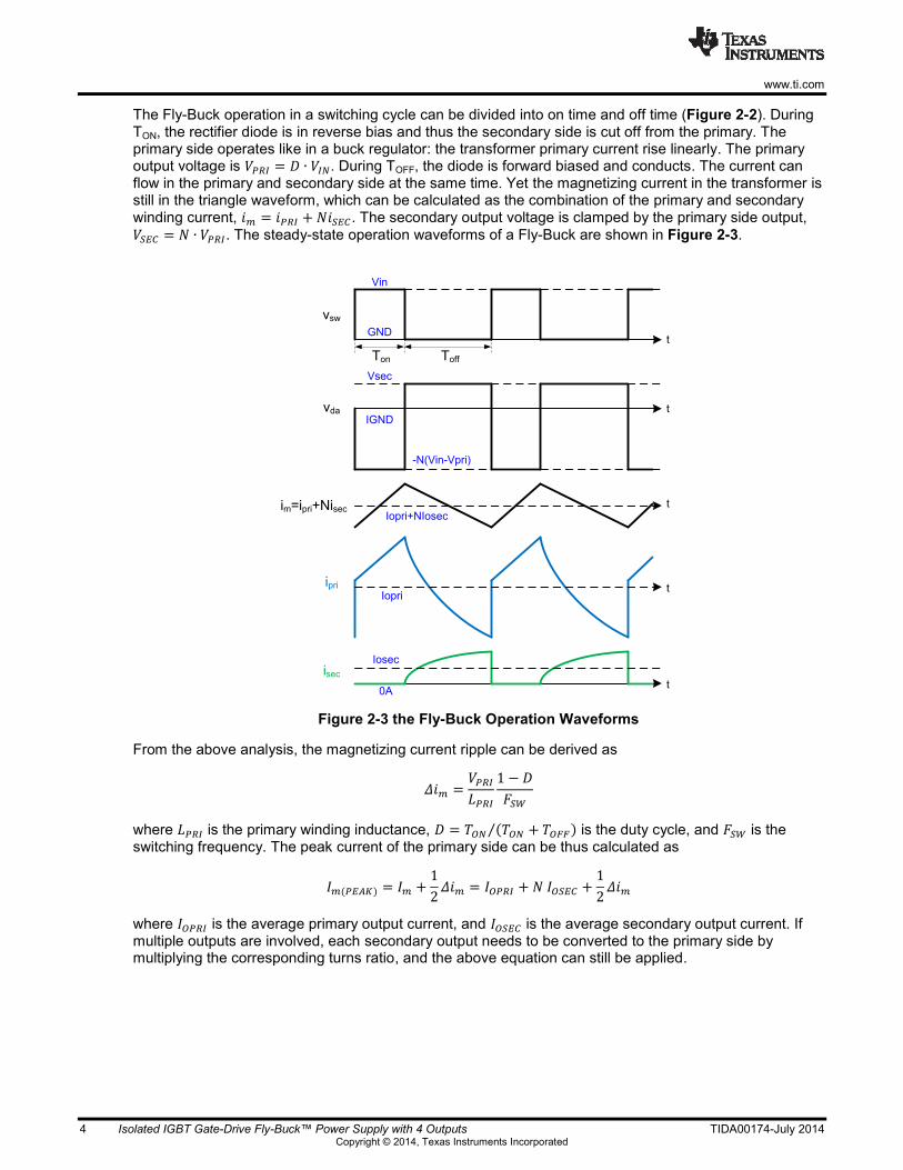
The Fly-Buck operation in a switching cycle can be divided into on time and off time (Figure 2-2). During TON, the rectifier diode is in reverse bias and thus the secondary side is cut off from the primary. The primary side operates like in a buck regulator: the transformer primary current rise linearly. The primary output voltage is . During TOFF, the diode is forward biased and conducts. The current can flow in the primary and secondary side at the same time. Yet the magnetizing current in the transformer is still in the triangle waveform, which can be calculated as the combination of the primary and secondary winding current, . The secondary output voltage is clamped by the primary side output,
. The steady-state operation waveforms of a Fly-Buck are shown in Figure 2-3.
Vin
GND
IGND
Vsec
-N(Vin-Vpri)
Iosec
Iopri
Iopri+NIosec
0A
vsw
vda
im=ipri+Nisec
ipri
isec
t
t
t
t
t
Ton Toff
Figure 2-3 the Fly-Buck Operation Waveforms
From the above analysis, the magnetizing current ripple can be derived as
where is the primary winding inductance, ( )⁄ is the duty cycle, and is the switching frequency. The peak current of the primary side can be thus calculated as
( )
where is the average primary output current, and is the average secondary output current. If multiple outputs are involved, each secondary output needs to be converted to the primary side by multiplying the corresponding turns ratio, and the above equation can still be applied.

www.ti.com
TIDA00174-July 2014 Isolated IGBT Gate-Drive Fly-Buck™ Power Supply with 4 Outputs 5 Copyright © 2014, Texas Instruments Incorporated
3 Fly-Buck Design Procedure
Here below is the design procedure of the Fly-Buck power supply for the IGBT gate driver bias.
3.1 Design Specification
The system-level requirements for this design are:
1. The isolated positive and negative rails should be +16V and -9V to power the isolated gate driver.
2. Continuous output power of 2.5W to drive each IGBT.
Input: 24V ± 20%
Output: Isolated 2×(+16V@100mA ; -9V@100mA)
Frequency: 350kHz
3.2 Circuit Parameter Design
1. Determine the primary-side output:
The primary-side, non-isolated output is set to 10.3V for several considerations. First, it is below the minimum 19V VIN, and the theoretical duty cycle will vary from 34 to 54 percent at the full VIN range, which is considered a balanced duty cycle. Optimally, it is favorable to have the Fly-Buck switching duty cycle below 50%. Because the Fly-Buck utilizes the duty off-time to transfer energy to the secondary side, and the high duty cycle will choke the current flow and affect the regulation. For this design, some tradeoff has to be made to accommodate the transformer turns ratio and the current limit of the LM5017. Additionally, the LM5017 can utilize this 10.3V to supply its own VCC bypassing the internal LDO, which is more efficient than powering VCC from Vin directly.
2. Determine the transformer turns ratio:
Based on the primary output to the isolated outputs ratio, the sec-to-pri turns ratio for the -9V output is 1:1.08, which is 1.62:1 for the +16V output. These turns ratios are rounded up to integer numbers for the convenience of the winding count. The +16V windings can share the ground pin with the -9V output, as long as the isolation between these two outputs is not required. This helps to reduce the size and save the pin count. The transformer winding configuration is shown in Figure 3-1.
Figure 3-1 Transformer winding configuration

www.ti.com
6 Isolated IGBT Gate-Drive Fly-Buck™ Power Supply with 4 Outputs TIDA00174-July 2014 Copyright © 2014, Texas Instruments Incorporated
3. Choose the inductance and switching frequency:
After knowing the turns ratio, the total average current in the primary winding can be calculated, which gives 0.51A. We choose a 60uH primary inductance. With the 350 kHz switching frequency, the peak current is thus calculated as 0.67A at maximum VIN = 30V, which is below the 0.7A peak-current limit.
4. Design the ripple injection network:
The COT control requires minimum external part count to make the IC switching stable. The ripple injection network is a RC network (shown in Figure 3-2) that generates a voltage ripple and has it injected to the FB pin.
SW
FB
LM5017COUT
VOUT
Rr
Cac
Cr
RFBB
RFBT
Figure 3-2 the Ripple Injection Network
The design principle and calculation tools of the ripple injection network can be found on the LM5017 product page on ti.com. The following RC parameters are set: Rr=40.2 kΩ, Cr=10 nF and Cac=1 nF.
www.ti.com
TIDA00174-July 2014 Isolated IGBT Gate-Drive Fly-Buck™ Power Supply with 4 Outputs 7 Copyright © 2014, Texas Instruments Incorporated
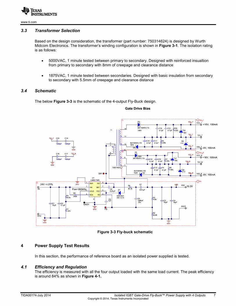
3.3 Transformer Selection
Based on the design consideration, the transformer (part number: 750314624) is designed by Wurth Midcom Electronics. The transformer’s winding configuration is shown in Figure 3-1. The isolation rating is as follows:
5000VAC, 1 minute tested between primary to secondary. Designed with reinforced insualtion from primary to secondary with 8mm of creepage and clearance distance
1875VAC, 1 minute tested between secondaries. Designed with basic insulation from secondary to secondary with 5.5mm of creepage and clearance distance
3.4 Schematic
The below Figure 3-3 is the schematic of the 4-output Fly-Buck design.
Figure 3-3 Fly-buck schematic
4 Power Supply Test Results
In this section, the performance of reference board as an isolated power supplied is tested.
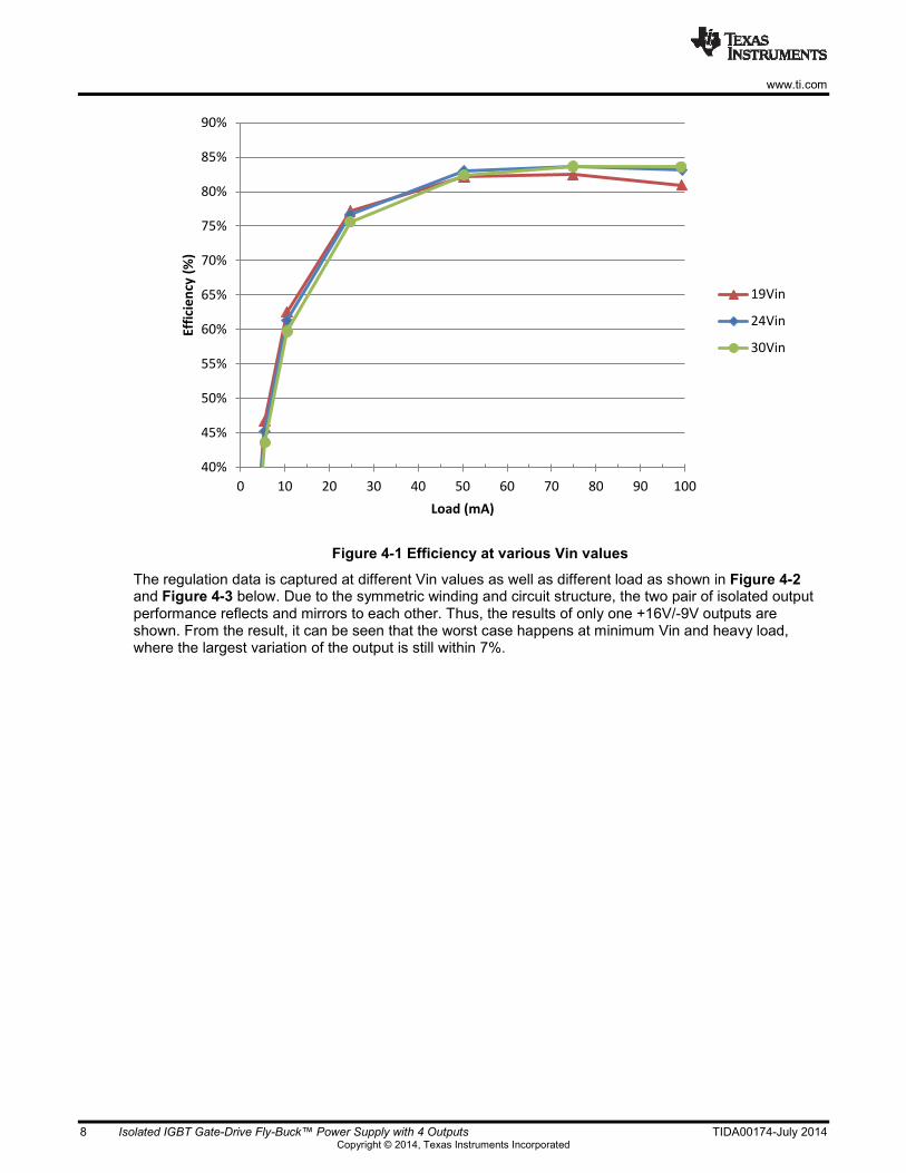
4.1 Efficiency and Regulation The efficiency is measured with all the four output loaded with the same load current. The peak efficiency is around 84% as shown in Figure 4-1.
www.ti.com
8 Isolated IGBT Gate-Drive Fly-Buck™ Power Supply with 4 Outputs TIDA00174-July 2014 Copyright © 2014, Texas Instruments Incorporated
Figure 4-1 Efficiency at various Vin values
The regulation data is captured at different Vin values as well as different load as shown in Figure 4-2 and Figure 4-3 below. Due to the symmetric winding and circuit structure, the two pair of isolated output performance reflects and mirrors to each other. Thus, the results of only one +16V/-9V outputs are shown. From the result, it can be seen that the worst case happens at minimum Vin and heavy load, where the largest variation of the output is still within 7%.
40%
45%
50%
55%
60%
65%
70%
75%
80%
85%
90%
0 10 20 30 40 50 60 70 80 90 100
Effi
cie
ncy
(%
)
Load (mA)
19Vin
24Vin
30Vin

www.ti.com
TIDA00174-July 2014 Isolated IGBT Gate-Drive Fly-Buck™ Power Supply with 4 Outputs 9 Copyright © 2014, Texas Instruments Incorporated
Figure 4-2 +16V and -9V Regulation at full load and no load over different Vin
Figure 4-3 +16V and -9V Regulation at 19V and 24V Vin over different load
-8%
-7%
-6%
-5%
-4%
-3%
-2%
-1%
0%
1%
2%
3%
4%
18 20 22 24 26 28 30 32
vari
atio
n (
%)
Vin (V)
-9V,75mA load +16V, 75mA load
-9V,no load +16V, no load
-12%
-10%
-8%
-6%
-4%
-2%
0%
2%
4%
0 25 50 75
vari
atio
n (
%)
Load (mA)
-9V, 19Vin +16V, 19Vin-9V, 24Vin +16V, 24Vin-9V, 30Vin +16V, 30Vin

www.ti.com
10 Isolated IGBT Gate-Drive Fly-Buck™ Power Supply with 4 Outputs TIDA00174-July 2014 Copyright © 2014, Texas Instruments Incorporated
4.2 Start Up The start-up of the power supply is tested under nominal 24V working voltage, and all four outputs were set at 100mA load. The below waveform shows the ramp-up of the isolated outputs, where Ch1 - Vin, Ch2 – +16V output, Ch3 – -9V output.
Figure 4-4 Start up at nominal Vin
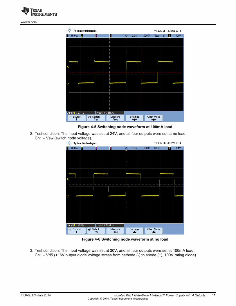
4.3 Switching Waveforms The stable switching of the Fly-Buck converter is examined at the switch node on the primary side and also checked at the secondary rectifier diodes to make sure the voltage spikes across are within the voltage rating. From the below test waveforms, we can find that the switching frequency remains relatively stable around 350kHz and the diode voltage stress is under the 100V rating with margin.
1. Test condition: The input voltage was set at 24V, and all four outputs were set at 100mA load. Ch1 – Vsw (switch node voltage)
www.ti.com
TIDA00174-July 2014 Isolated IGBT Gate-Drive Fly-Buck™ Power Supply with 4 Outputs 11 Copyright © 2014, Texas Instruments Incorporated
Figure 4-5 Switching node waveform at 100mA load
2. Test condition: The input voltage was set at 24V, and all four outputs were set at no load. Ch1 – Vsw (switch node voltage).
Figure 4-6 Switching node waveform at no load
3. Test condition: The input voltage was set at 30V, and all four outputs were set at 100mA load.
Ch1 – Vd5 (+16V output diode voltage stress from cathode (-) to anode (+), 100V rating diode)

www.ti.com
12 Isolated IGBT Gate-Drive Fly-Buck™ Power Supply with 4 Outputs TIDA00174-July 2014 Copyright © 2014, Texas Instruments Incorporated
Figure 4-7 +16V output diode voltage waveform at highest Vin at full load
4. Test condition: The input voltage was set at 30V, and all four outputs were set at 100mA load. Ch1 – Vd2 (-9V output diode voltage stress from cathode (-) to anode (+), 100V rating diode)
Figure 4-8 +16V output diode voltage waveform at highest Vin at full load
4.4 Load Transients
1. +16V Output Load Step Test condition: Vin = 24V, +16V output load from 0A to 100mA, no load on other outputs. Ch1- +16V output (AC mode), Ch4- +16V output current

www.ti.com
TIDA00174-July 2014 Isolated IGBT Gate-Drive Fly-Buck™ Power Supply with 4 Outputs 13 Copyright © 2014, Texas Instruments Incorporated
Figure 4-9 +16V output load transient
2. -9V Output Load Step Test condition: Vin = 24V, -9V load from 0A to 100mA, no load on other outputs. Ch1- -9V output (AC mode), Ch4- -9V output current
Figure 4-10 -9V output load transient
4.5 Output Voltage Ripples Test condition: The input voltage was set at 24V, and all four outputs were set at 100mA load. Ch1 - +16V output (AC coupled)

www.ti.com
14 Isolated IGBT Gate-Drive Fly-Buck™ Power Supply with 4 Outputs TIDA00174-July 2014 Copyright © 2014, Texas Instruments Incorporated
Figure 4-11 +16V output voltage ripple at full load
Ch1 - -9V output (AC coupled)
Figure 4-12 +16V output voltage ripple at full load

www.ti.com
TIDA00174-July 2014 Isolated IGBT Gate-Drive Fly-Buck™ Power Supply with 4 Outputs 15 Copyright © 2014, Texas Instruments Incorporated
5 System Demo
To validate the reference design function in an IGBT system, we modified the C2000 High Voltage Single Phase Inverter Development Kit (TMDSHV1PHINVKIT) from TI to create a system demo. It is a full bridge DC/AC inverter with 4 IGBTs, and the input is 400V DC and the output is 110/220V AC selectable. The kit uses 4 driver card boards for driving the IGBT, which makes it convenient to replace them with the Fly-Buck solution. The original driver card design uses the opto-coupler gate driver and open-loop forward converter as the bias power. The 4-output Fly-Buck design can supply two IGBT drivers, and thus only two Fly-Buck driver cards are needed. The opto-coupler gate drivers are added to the design.
The two drivers are biased by the Fly-Buck isolated power supply design shown in Figure 3-3. The new driver card will take the PWM signals from the C2000 control card, and drive two IGBTs. The Fly-Buck driver card board is shown in Figure 5-1. The board is stretched longer than the actual component cover area, as the two connectors on the board are positioned to make compatible with the headers on the base board of the inverter kit.
Figure 5-1 Fly-Buck IGBT Driver Card Board
The inverter system with the plug-in Fly-Buck driver cards is shown in Figure 5-2.
Figure 5-2 Full Bridge Inverter with Fly-Buck IGBT Driver Cards

www.ti.com
16 Isolated IGBT Gate-Drive Fly-Buck™ Power Supply with 4 Outputs TIDA00174-July 2014 Copyright © 2014, Texas Instruments Incorporated
6 System Setup and Test
In this section, the demo setup guide is presented, and the system is tested.
6.1 System Setup
The Fly-Buck supply takes 24V input, but the inverter base board requires 15V as system power. Therefore, an external 24V DC supply is needed to supply the Fly-Buck driver card. The board configuration is as follows:
1. Configure jumpers on the inverter board: open JP1, JP2, JP3, short JP4, JP5, JP6
2. Plug in the Fly-Buck driver cards and the MCU control card to the base board as shown in Figure 5-2.
3. Connect external DC power supplies: tie +15V supply to JP1, tie +24V supply to JP2, and GND pins are
accessible at connector CN5’s pin 9, 10 as shown in Figure 6-1.
4. Connect the USB cable from the control card to the computer and turn on the +15V power supply
Figure 6-1 Inverter Board Auxiliary Power Connection
5. Use the Code Composer Studio (CCS) to load the inverter control program to the control card.
6. Check if the system is function correctly. The detailed program setting and the inverter kit information can
be found in the Application Report, High-Voltage Solar Inverter DC-AC Kit (sprabr5).
7. Connect the DC Bus input connector (CON1) to the high voltage supply (400V DC), and the load to the
inverter output (CON2)

www.ti.com
TIDA00174-July 2014 Isolated IGBT Gate-Drive Fly-Buck™ Power Supply with 4 Outputs 17 Copyright © 2014, Texas Instruments Incorporated
8. Use the GUI or the on-board button SW1 to control the inverter on/off.
6.2 System Test
After the system is set up, the high voltage DC bus can be applied to the inverter, and the IGBT in full bridge connection will be switched in SPWM. The Figure 6-2 shows the waveforms of the 120VAC/60Hz output voltage, current, and the gate drive signal of one IGBT. The input is set at 380V DC and the load is 50Ω resistive load. From the oscilloscope, the RMS of the output AC current is 2.4A.
Figure 6-2 Output of the Inverter and the Driver waveform
Since the Fly-Buck power supply has the advantage of the primary side regulation and thus good line regulation, the +24V auxiliary power doesn’t need to be tightly regulated. While the inverter is operating, the +24V input can be varied +/-20%, and it won’t affect the bias voltage level and all the drivers still operate stably. The Figure 6-3 and Figure 6-4 are the IGBT gate-to-emitter voltage (Vge) waveforms of one arm of the IGBT bridge captured at different Vin to the Fly-Buck supply (the Ch1 is the low side IGBT Vge, while the Ch3 is the high side IGBT Vge). It can be seen that the Vge switching remains almost unaffected by the change of the input voltage. The ΔVge from +16V to -9V is kept at 25V, and the dead time is also unchanged. As a comparison, the original driver cards are also tested, and the results are shown in Figure 6-5 and Figure 6-6. The difference is significant. There’s no line/load regulation with the open-loop converter, and the ΔVge varies from 24.5V to 30V even with a +/-10% Vin change. Also, the dead time is slightly affected.
The disturbance on the gate drive bias voltage is undesirable, as it will increase the switching loss and lower the system efficiency. Furthermore, for high power application, it could impact the system reliability and the IGBT life span, as the risk of false turn on and shoot through caused by the bias voltage deviation increases. Therefore, the Fly-Buck power supply for its robust performance is well suited for the IGBT gate drive bias.

www.ti.com
18 Isolated IGBT Gate-Drive Fly-Buck™ Power Supply with 4 Outputs TIDA00174-July 2014 Copyright © 2014, Texas Instruments Incorporated
Figure 6-3 Vge signal at 80% of Vin with Fly-Buck
Figure 6-4 Vge signal at 120% of Vin with Fly-Buck
Figure 6-5 Vge signal at 90% of Vin with Open-loop Converter
LS IGBT Vge
Vin ↑20%
Vin ↓10%
HS IGBT Vge
25V ΔVgate
24.5V ΔVgate
Vin ↓20%
1.58us Dead time
LS IGBT Vge
25V ΔVgate
HS IGBT Vge
1.58us Dead time
1.58us Dead time

www.ti.com
TIDA00174-July 2014 Isolated IGBT Gate-Drive Fly-Buck™ Power Supply with 4 Outputs 19 Copyright © 2014, Texas Instruments Incorporated
Figure 6-6 Vge signal at 110% of Vin with Open-loop Converter
Vin ↑10%
30V ΔVgate
1.60us Dead time

IMPORTANT NOTICE FOR TI REFERENCE DESIGNSTexas Instruments Incorporated ("TI") reference designs are solely intended to assist designers (“Buyers”) who are developing systems thatincorporate TI semiconductor products (also referred to herein as “components”). Buyer understands and agrees that Buyer remainsresponsible for using its independent analysis, evaluation and judgment in designing Buyer’s systems and products.TI reference designs have been created using standard laboratory conditions and engineering practices. TI has not conducted anytesting other than that specifically described in the published documentation for a particular reference design. TI may makecorrections, enhancements, improvements and other changes to its reference designs.Buyers are authorized to use TI reference designs with the TI component(s) identified in each particular reference design and to modify thereference design in the development of their end products. HOWEVER, NO OTHER LICENSE, EXPRESS OR IMPLIED, BY ESTOPPELOR OTHERWISE TO ANY OTHER TI INTELLECTUAL PROPERTY RIGHT, AND NO LICENSE TO ANY THIRD PARTY TECHNOLOGYOR INTELLECTUAL PROPERTY RIGHT, IS GRANTED HEREIN, including but not limited to any patent right, copyright, mask work right,or other intellectual property right relating to any combination, machine, or process in which TI components or services are used.Information published by TI regarding third-party products or services does not constitute a license to use such products or services, or awarranty or endorsement thereof. Use of such information may require a license from a third party under the patents or other intellectualproperty of the third party, or a license from TI under the patents or other intellectual property of TI.TI REFERENCE DESIGNS ARE PROVIDED "AS IS". TI MAKES NO WARRANTIES OR REPRESENTATIONS WITH REGARD TO THEREFERENCE DESIGNS OR USE OF THE REFERENCE DESIGNS, EXPRESS, IMPLIED OR STATUTORY, INCLUDING ACCURACY ORCOMPLETENESS. TI DISCLAIMS ANY WARRANTY OF TITLE AND ANY IMPLIED WARRANTIES OF MERCHANTABILITY, FITNESSFOR A PARTICULAR PURPOSE, QUIET ENJOYMENT, QUIET POSSESSION, AND NON-INFRINGEMENT OF ANY THIRD PARTYINTELLECTUAL PROPERTY RIGHTS WITH REGARD TO TI REFERENCE DESIGNS OR USE THEREOF. TI SHALL NOT BE LIABLEFOR AND SHALL NOT DEFEND OR INDEMNIFY BUYERS AGAINST ANY THIRD PARTY INFRINGEMENT CLAIM THAT RELATES TOOR IS BASED ON A COMBINATION OF COMPONENTS PROVIDED IN A TI REFERENCE DESIGN. IN NO EVENT SHALL TI BELIABLE FOR ANY ACTUAL, SPECIAL, INCIDENTAL, CONSEQUENTIAL OR INDIRECT DAMAGES, HOWEVER CAUSED, ON ANYTHEORY OF LIABILITY AND WHETHER OR NOT TI HAS BEEN ADVISED OF THE POSSIBILITY OF SUCH DAMAGES, ARISING INANY WAY OUT OF TI REFERENCE DESIGNS OR BUYER’S USE OF TI REFERENCE DESIGNS.TI reserves the right to make corrections, enhancements, improvements and other changes to its semiconductor products and services perJESD46, latest issue, and to discontinue any product or service per JESD48, latest issue. Buyers should obtain the latest relevantinformation before placing orders and should verify that such information is current and complete. All semiconductor products are soldsubject to TI’s terms and conditions of sale supplied at the time of order acknowledgment.TI warrants performance of its components to the specifications applicable at the time of sale, in accordance with the warranty in TI’s termsand conditions of sale of semiconductor products. Testing and other quality control techniques for TI components are used to the extent TIdeems necessary to support this warranty. Except where mandated by applicable law, testing of all parameters of each component is notnecessarily performed.TI assumes no liability for applications assistance or the design of Buyers’ products. Buyers are responsible for their products andapplications using TI components. To minimize the risks associated with Buyers’ products and applications, Buyers should provideadequate design and operating safeguards.Reproduction of significant portions of TI information in TI data books, data sheets or reference designs is permissible only if reproduction iswithout alteration and is accompanied by all associated warranties, conditions, limitations, and notices. TI is not responsible or liable forsuch altered documentation. Information of third parties may be subject to additional restrictions.Buyer acknowledges and agrees that it is solely responsible for compliance with all legal, regulatory and safety-related requirementsconcerning its products, and any use of TI components in its applications, notwithstanding any applications-related information or supportthat may be provided by TI. Buyer represents and agrees that it has all the necessary expertise to create and implement safeguards thatanticipate dangerous failures, monitor failures and their consequences, lessen the likelihood of dangerous failures and take appropriateremedial actions. Buyer will fully indemnify TI and its representatives against any damages arising out of the use of any TI components inBuyer’s safety-critical applications.In some cases, TI components may be promoted specifically to facilitate safety-related applications. With such components, TI’s goal is tohelp enable customers to design and create their own end-product solutions that meet applicable functional safety standards andrequirements. Nonetheless, such components are subject to these terms.No TI components are authorized for use in FDA Class III (or similar life-critical medical equipment) unless authorized officers of the partieshave executed an agreement specifically governing such use.Only those TI components that TI has specifically designated as military grade or “enhanced plastic” are designed and intended for use inmilitary/aerospace applications or environments. Buyer acknowledges and agrees that any military or aerospace use of TI components thathave not been so designated is solely at Buyer's risk, and Buyer is solely responsible for compliance with all legal and regulatoryrequirements in connection with such use.TI has specifically designated certain components as meeting ISO/TS16949 requirements, mainly for automotive use. In any case of use ofnon-designated products, TI will not be responsible for any failure to meet ISO/TS16949.
Mailing Address: Texas Instruments, Post Office Box 655303, Dallas, Texas 75265Copyright © 2014, Texas Instruments Incorporated