jay amrit kapitza resistance at niobiumsuperfluid he interfaces
TRANSCRIPT

Kapitza Thermal Boundary Resistance

Kapitza Thermal Boundary Resistance at Niobium/Superfluid He interfaces in SRF cavities
Jay AMRIT
LIMSI-CNRS , Paris-Sud University, [email protected]
In collaboration with
Claire ANTOINE(CEA, Saclay)
Thin Films and New Ideas for RF Superconductivity, Padova, 2014

Part I : Introduction on KTBR
Why is it important?/Model predictions
Part II : Experiments with Nb: bulk purity & surface statePoly-crystals
Single crystals
Comparison and impact on SRF cavities
Part III : New analysis & ongoing work
Importance of nanoscale surface roughness
Kapitza resistance at grain boundaries in Nb
Pressure dependency of KTBR : What would happen to
cavity performance if we increased the pressure to 25 bars?
Summary & possible future studies…
Outline
Thin Films and New Ideas for RF Superconductivity, Padova, 2014

Introduction: Discovery of thermal boundary resistance
Pyotr L. KAPITZA (1894-1984)
-prix Nobel 1978-
Discovered in 1941 by Kapitza
Cooling of Solids with Superfluid Helium
Superfluidity He
• Discovered 1938
•Temperatures < 2 K (-271°C)
•Quasi-infinite thermal conductivityCopper
Superfluid4He
Q
Thermal boundary resistance = Kapitza resistance
Impossible to reach zero absolute temperature by direct cooling
Fountain effect
Thin Films and New Ideas for RF Superconductivity, Padova, 2014

Introduction: Fundamental interest in Kapitza resistance
TBR is an important phenomenon at low temperatures
310S
K
T
T
810L
K
T
T
Typical temperature gradient with temperature jump over atomic distances
1 mm1 mm
TL
TS
Superfluid HeSolid (Cu)
TK
x
Kcu ~1 W/(mK) KHe ~ 800 x KCu
LK TT 810
SK TT 310
For Nb :NbK TT )1000100(
Kapitza length KK RKL
kmL HeIIK 8,
cmL CuK 10,
Te
mp
era
ture
Thin Films and New Ideas for RF Superconductivity, Padova, 2014

Introduction: Kapitza resistance in SRF cavities
Electrical surface resistance :
2/T
0RF
acc
RF
dt)t,z(ET
2)m/MV(EAccelerating field :
Quality factor QO :
dVE2
1U v
2o (stored energy)
Power dissipatedEnergy stored per sec
q
UωQo
(3-4 nano ohms)
Heat dissipation in inner walls : //B penetrates ~50 nm into walls
Joule effect
residualc2
s R)T/T76.1exp()T/(AR
Thin Films and New Ideas for RF Superconductivity, Padova, 2014

e
He IINb
Tin
THe
KapitzaT
q
B
TinTbath
ToutRK)T(K
e
q
Ks
oacc
RK
eR
TE
1
8
2/12
Cavités ellipsoïdales : ]/[][ 4 mMVaccmT EB
2//
2
1BRq s
o
Power dissipation :
qRK
eTTT KHein
Temperature jump :
Kapitza resistance
Introduction: simple thermal model
Accelerating field dependence on K and RK
A strong RK limits the Eacc !
Thin Films and New Ideas for RF Superconductivity, Padova, 2014

Heat transport in superfluid Helium
•Interaction potential between 2 atoms determines
heat transport in He
•Energy is rapidly distributed between atoms
•Only longitudinal (acoustic) phonons transport heat
•Other excitations : rotons, maxons, vortices
240Lc m.s-1
= cLk
Dispersion relation of Helium
Thin Films and New Ideas for RF Superconductivity, Padova, 2014

Heat transport in superfluid Helium
240Lc m.s-1
= cLk
Dispersion relation of Helium
•Unique characteristics of heat and mass transfer
•Mixture of two fluids (& not two phases) :
•Momentum density :
Two fluid model of He II (Tisza, 1938)
Normal component : n n ns
Superfluid component : s s 0ss
sn
q
Two different sounds
First sound (240 m/s) pressure wave & both fluids move in phase
Second sound (~20m/s): temperature wave & fluids move in opposite directions
nnssJ
ssnn 0
Normal component = source & Superfluid component = sink
ns
Thin Films and New Ideas for RF Superconductivity, Padova, 2014

Heat transport in Niobium in a nutshell
Lattice bcc, a =3.29 A
Atoms oscillate around their equilibrium positions, producing vibrational waves
Acoustic modes ( = vk)
•3 branches : longitudinal & 2 transverse
•Each branch has N modes
•Mode = (, k)=quantum of acoustic vibration (phonon)
111
100
L
L
T
T
J. Phys. C 2, 421 (1969)
Longitudinal Transverse
Thin Films and New Ideas for RF Superconductivity, Padova, 2014

Thermal boundary resistance: how does it come about at theNb/He II interface?
The key is to determine
the transmission of
phonons
Very small overlap
in wave vectors
Dispersion relation of Nb and He
0
1
2
3
4
5
6
0 0,5 1 1,5 2 2,5
Nb dispersion relation
freq (THz)Freq (Thz)Freq (THz)
q (A-1
)
Nb (111)
L
T
He II
Thin Films and New Ideas for RF Superconductivity, Padova, 2014

Number of phonons of wave vector k incident at an angle q per unit time :
Bose-Einstein distribution
Heat energy transmitted :
Energy incident per branch and for a given k :
Thermal resistance
q
cosc
4
ddk)k(g)T,(nN b,1b,1
1Tk1e)T,(n B
3b
2
3
3
c
d4
)L/2(
kddk)k(g
N° of modes with wavevector k for a given branch
b,1N
321 T
ARK
Thermal boundary resistance: formal approach
bb
K
dcdT
Tng
T
q
R
q
qqq
0
2/
00 sincos2
),()(
4
11
Specific heat
21121
4
11
D
K
CT
q
R
b
b dcdgTnQQq
q
qqq0
2/
001221 sincos)(),(
2
1
Average transmission
(phonons /)
Thin Films and New Ideas for RF Superconductivity, Padova, 2014

Kapitza resistance model : Acoustic mismatch model (AMM) (Khalatnikov, 1952)
•Parallel component of momentum
•Frequency
Conservation laws at the interface:
//S
//L pp
SL
Snell’s lawS
S
L
L
c
sin
c
sin qq
S
L
SL
SLAM
Z
Z
ZZ
ZZ 44)(
2
q
Transmission coefficient is due to discontinuity in sound velocity & density
,LLL cZ
,SSS cZ
Lq
LL kp
SS kp
jcoskisinkk SSSSS
jkikk LLLLL
qq cossin
Sq
240Lc m.s-1
53cLq
Critical cone in superfluid limits transmission of phonons !!
5068, LNbc m.s-1 m.s-12092, TNbc002.04
)(20
qq d
c
AMAM
Nb
He
Thin Films and New Ideas for RF Superconductivity, Padova, 2014

Kapitza resistance models : diffuse mismatch model (DMM)
“Trick” to increase phonon transmission in model
Phonons loose “memory” of former states
No physical restrictions on scattering mechanism !!
NO dependency on interface properties
)(t1
)(t2 )(r2
)(r1
1)(r)(t 11
1)(r)(t 22
2211 )()( qtqt
5.0~q
q1)(t
1
2
11
)(t)(r 21
He II
Nb
DMM phonon transmission is increased by two orders of magnitudeHow the diffuse scattering comes about is not explained in this model!
(at equilibrium)
Swartz & Pohl 1989
Thin Films and New Ideas for RF Superconductivity, Padova, 2014

0
1
2
3
4
5
40
60
80
100
120
1,5 1,6 1,7 1,8 1,9 2 2,1
Khalatnikov & Dm for NbHeII
RKhalat (cm2K/W)Rdm (cm2K/W)
T (K)
AM model
DM model
Theoretical Model predictions of Kapitza resistance for Nb/HeII
Depends on properties of liquid He
Depends on properties of Nb
ExperimentsNb/HeII
The Kapitza resistance at a solid/ superfluid He II interface is anomalous !
Thin Films and New Ideas for RF Superconductivity, Padova, 2014

Experimental Cell
Nb disc sampleHeater
Carbon Thermometers
Q
superfluid
To
T1 4He Filling line
Temperature profile across a sample
K : thermal conductivitye : sample thickness
K
e
Q
)TT(SR
.K2
01
To
T1
RKQTo
RK
T
Experiments : cell configuration & method
Thin Films and New Ideas for RF Superconductivity, Padova, 2014

Polycrystalline Niobium: 4 different bulk & surface treatments
100 µm
chemically etched
250 µm
annealed and chemically
etched
Light Heavy
250 µm
electropolished
50 µm
annealed, chemically
etched & electropolished
Micrographics of surfaces
1
2
3
4
RRR 178
RRR 178
RRR 647
RRR 647
4.08.1σ
25.085.0σ
4.03.1σ
1.02.0σ
)mμ(σK2.4
K300
ρ
ρRRR

0.5
1
1.5
2
2.5
3
3.5
4
4.5
1.5 1.6 1.7 1.8 1.9 2 2.1 2.2
RK
(cm
2K
.W-1
)
Temperature (K)
1
3
4
2
Polycrystalline Niobium : RK results
Sample, RRR Surface Treatment s (µm)# RK (cm2K4W-1)
#1, 178 CP(~30 µm) 1.8 + 0.4 10.7T-3.55
#2, 178 EP 0.85 + 0.25 21.3T-4.11
#3, 647 Annealed +CP 1.3 + 0.4 16.1T-3.93
#4, 647▲ Annealed +EP 0.2 + 0.1 19.1T-3.61
Bulk purity :
Change in K by a factor of 5 (annealing)
RK changes by ~15% only
(1 & 3)
Surface Roughness :
Smaller surface roughness s leads to
higher RK (independent of bulk purity)
Thin Films and New Ideas for RF Superconductivity, Padova, 2014

Polycrystalline Niobium : RK compared to total thermal resistance
20
30
40
50
60
70
80
1.5 1.6 1.7 1.8 1.9 2 2.1 2.2
T(K)
4
3
2
1
K
eR
R
K
K
RRR 647
annealed
RRR 178
•RK constitutes ~70% of total thermal resistance
•Higher bulk purity and lower temperatures lead to a stronger impact of RK
•RK is the key parameter for cooling cavities
Thin Films and New Ideas for RF Superconductivity, Padova, 2014

Polycrystalline Niobium : Which samples are best?
20
30
40
50
60
70
80
1.5 1.6 1.7 1.8 1.9 2 2.1 2.2
T(K)
4
3
2
1
K
eR
R
K
K
RRR 647
annealed
RRR 178
30
40
50
60
70
80
90
1,5 1,6 1,7 1,8 1,9 2 2,1
T(K)
3
4
1
2
2/1
1
K
eR
E
K
acc
Annealed and CP is best !
Thin Films and New Ideas for RF Superconductivity, Padova, 2014
•RK constitutes ~70% of total thermal resistance
•Higher bulk purity and lower temperatures lead to a stronger impact of RK
•RK is the key parameter for cooling cavities

µm
-14
-13
-12
-11
-10
-9
-8
-7
-6
-5
-4
-3
-2
-1
0
1
2
3
4
5
6
7
8
9
10
11
µm
-4
-3.5
-3
-2.5
-2
-1.5
-1
-0.5
0
0.5
1
1.5
2
1
1,5
2
2,5
3
3,5
4
4,5
1,5 1,6 1,7 1,8 1,9 2 2,1
Temperature (K)
Damaged
Layer
Chemically
polished
Single Crystal (111) Niobium : Impact of surface state on RK
Niobium ingot ( = 5 cm) , RRR = 300
Crystallographic orientation (111) – EBSD technique
2 sample surfaces :
Damaged Layer sample• Electrical discharge machining (EDM)• large dumps (25µm)• impurities (O2, Cu, Zn,…)• velvet-like texture, s ~ 7µm
Chemically polished sample• BCP- removal of 30µm• s ~ 1µm
Thin Films and New Ideas for RF Superconductivity, Padova, 2014

Single Crystal Niobium : Phonon-dislocation interactions in skin layer
1
1,5
2
2,5
3
3,5
4
4,5
1,5 1,6 1,7 1,8 1,9 2 2,1
Temperature (K)
Damaged
Layer
Chemically
polished
EDM creates dislocations within narrow layer ( µm)
Thermal Resistivity Model for Nb (W. Wasserbäch)
(Philos. Mag. A.38 401 (1978))
Random distribution of dislocations:
(cm3K3/W)2
91005.3T
NR d
dp
ddpCPKDLK RRR ,,Analysis :
1~d
Plausible dislocation density which explains results
12109~ dN cm-2
Important result indicating scattering/reflection of energy back into Nb due to dislocations &
impurities (contradicts theoretical ideas)
~ 40%
Thin Films and New Ideas for RF Superconductivity, Padova, 2014

Relative importance of RK
compared to (RK
+ e/K)
0.5
0.6
0.7
0.8
0.9
1.5 1.6 1.7 1.8 1.9 2 2.1
RK/[R
K+(d/K)]
T(K)
(a)
(b)
(c)
(d)
polycrystallineRRR = 647
single crystal
Polycrystalline and Single crystal Nb
CP
EP
DL
CP
Single crystals :
Relative importance of RK increases with T
Polycrystalline Nb :
Relative importance of RK decreases with T
RK constitutes ~75% at T~1.8K for
chemically polished polycrystalline
& single crystals
Thin Films and New Ideas for RF Superconductivity, Padova, 2014

0,4
0,5
0,6
0,7
0,8
0,9
1,5 1,6 1,7 1,8 1,9 2 2,1
Nb crystal with Damaged LayerNb crystal _chemically polishedCP polycrystalline Nb (sample 3)
Temperature (K)
2/1
1
K
eR
E
K
acc
Comparing polycrystalline to single crystals
Annealed & CP polycrystalline
is strictly equivalent to CP
single crystal
Surface roughness are the
same in both cases!
Thermal point of view …
Thin Films and New Ideas for RF Superconductivity, Padova, 2014

- roughness length
- root mean roughness height
- inclination of roughness
New analysis using resonant scattering at Nb/HeII interfaceI. N. Adamenko & I. M. Fuks, JETP, 32, 1123 (1971)
s
He II
Nb surface
)r(ζ
Nature of phonon scattering is defined by s, l and Amplification of heat flux due to Multiple resonant phonon scattering
Solid surface is characterized at a given scale length by :
σ
σ2γ
(roughness)
ideal interface
l = phonon wavelength
Phonon wavelength =
Transmission coefficient =
2
2311l
s AM
)(
3
8.3)(
KT
nm
Tk
hcnm
B
L l
2
169
l
s
l
sf
l
s fQQ o
2
2
11
Thin Films and New Ideas for RF Superconductivity, Padova, 2014

Impact of Nanoscale surface roughness on RK
(new)
20
30
40
50
60
1,5 1,6 1,7 1,8 1,9 2 2,1
Roughness analysis-single & poly crystals
tau rough/tau 0Tau rough/tau0
Temperature (K)
Nb Polycrystal
Annealed + chemically polished
(RRR 647)
Nb Single crystal
Chemically polished
(RRR 300)
• RK of ideal surface is >> RK of real surface
• Resonant scattering is ~40 times more effective
0,3
0,35
0,4
0,45
0,5
0,55
0,6
1,5 1,6 1,7 1,8 1,9 2 2,1
Polycryst sample 3_JLTP2000 _ also called Ktcbis
sigma/lamda(sigma/lamda)CP
T (K)
5.03.0~
l
s
Ratio of Surface Roughness to
phonon wavelength
Selective diffuse resonant scattering
enhances transmission
Re
son
ant
scat
teri
ng
: ac
ou
stic
imp
ed
ance
Thin Films and New Ideas for RF Superconductivity, Padova, 2014

0,5
0,6
0,7
0,8
0,9
1
1,5 1,6 1,7 1,8 1,9 2 2,1
Polycryst sample 3_JLTP2000 _ also called Ktcbis
sigma_poly 3sigma (nm)_single CP
s (nm)
T(K)
Nb polycrystal
Nb single crystal
Su
rfa
ce
Rou
gh
ne
ss
Effective heat transfer
between Niobium and He II
occurs at scales less than
a nanometer
Impact of Nanoscale surface roughness on RK
(in progress)
Thin Films and New Ideas for RF Superconductivity, Padova, 2014

Pressure dependency of Kapitza resistance Will cooling of SRF cavities be more efficient if the He II pressure is increased to 25 bars?
3000
3500
4000
4500
5000
5500
6000
6500
0 5 10 15 20 25
Impédance acoustique de l'HeII
en fonction de la pression
T = 0.10KT = 0.20KT = 0.30KT = 0.40KT = 0.50KT = 0.60KT = 0.70KT = 0.80KT = 0.90KT = 1.00KT = 1.10KT = 1.20KT = 1.30KT = 1.40KT = 1.50KT = 1.60KT = 1.70KT = 1.80KT = 1.90KT = 2.00K
P (atm)
LLHe cZ
changes by ~80%
Aco
ustic im
pe
da
nce
of L
iqu
id H
e
cL and L increases with pressure
Nb
He
HeNb
HeNbAM
Z
Z
ZZ
ZZ 4
)(
42
Transmission
Coefficient
Niobium
He II
Thin Films and New Ideas for RF Superconductivity, Padova, 2014

Pressure dependency of Kapitza resistance Will cooling of SRF cavities be more efficient if the He II pressure is increased to 25 bars?
3000
3500
4000
4500
5000
5500
6000
6500
0 5 10 15 20 25
Impédance acoustique de l'HeII
en fonction de la pression
T = 0.10KT = 0.20KT = 0.30KT = 0.40KT = 0.50KT = 0.60KT = 0.70KT = 0.80KT = 0.90KT = 1.00KT = 1.10KT = 1.20KT = 1.30KT = 1.40KT = 1.50KT = 1.60KT = 1.70KT = 1.80KT = 1.90KT = 2.00K
P (atm)
LLHe cZ
changes by ~80%
Aco
ustic im
pe
da
nce
of L
iqu
id H
e
cL and L increases with pressure
Nb
He
HeNb
HeNbAM
Z
Z
ZZ
ZZ 4
)(
42
Transmission
Coefficient
0
1
2
3
4
5
6
7
150
200
250
0 5 10 15 20 25
P (bar)
~1.8K
2
l
s
Silicon crystal (111)
Niobium
He II
~80% change in acoustic impedance of He
NO change in transmission!
Thin Films and New Ideas for RF Superconductivity, Padova, 2014

0,2
0,4
0,6
0,8
1
1,2
1,4
1,6 1,7 1,8 1,9 2 2,1 2,2
Gra
in-g
rain
RK(c
m2K
/W)
T(K)
RK
~2T-3
(cm2K/W)
RKy
RKx
Kapitza resistance RG-G at grain boundaries in polycrystalline Nb
O
GG
o
lpolycrysta
KRnd
n
KK
)1(1
GGR Kapitza resistance at
grain-grain boundaries
Thermal conductivity of Nb :
oK Casimir thermal conductivity
n Nb. of grains
Anisotropy in heat flow through cavity walls:
-grain size d
-grain distribution
In plane
Cross plane
Solid-solid model
Thin Films and New Ideas for RF Superconductivity, Padova, 2014
KGG
acc
RRn
)1n(
d
e
1E

•Cooling of cavities is controlled by K and RK
•As purity of Nb improves, RK dominates
•Surface quality (chemical purity, structural order, surface roughness…) rather
than effective surface area
•Poly-crystals : Annealed + CP + s ~ 1.2µm is better than
Annealed + electro-polished
•Single crystals : Chemically polished (RRR 300) give better performance
•Thermo-mechanical history of sample : dislocations due to machining
•Equivalence in performance with poly-crystals and single crystals
• is important parameter
•Presence of dislocations and/or impurities increase RK
•Raising the pressure to 25 bars changes impedance by ~80%, but no effect on RK
•RK is anomalous – cannot be explained by acoustic mismatch theory
•New analysis : Resonant scattering of phonons from nanoscale roughnesses
Summary
KeRK /
1
Thin Films and New Ideas for RF Superconductivity, Padova, 2014
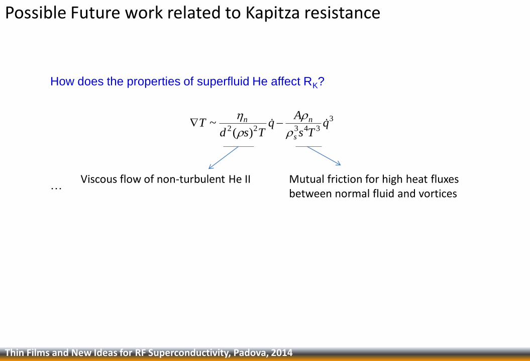
Possible Future work related to Kapitza resistance
How does the properties of superfluid He affect RK?
…
3
34322 )(~ q
Ts
Aq
TsdT
s
nn
Viscous flow of non-turbulent He II Mutual friction for high heat fluxesbetween normal fluid and vortices
Thin Films and New Ideas for RF Superconductivity, Padova, 2014

Kapitza resistance under High heat fluxes ?
32 )(25.0)()(5.11 TTTTTT
TTcorrect
32
0,
)(25.0)()(5.11 TTTTTT
R
q
TR
KcorrectK
Possible Future work related to Kapitza resistance
Radiation model for heat flux :
)( 441 LTTq TTT L 1
with
For 5.0T
T
2
0KK
RR we have
Thin Films and New Ideas for RF Superconductivity, Padova, 2014

Possible Future work related to Kapitza resistance
-Convection in liquid
-Nucleate boiling
-Film boiling
- Development of Turbulence & attenuation
of second sound
Physics of quantum fluids
Thin Films and New Ideas for RF Superconductivity, Padova, 2014
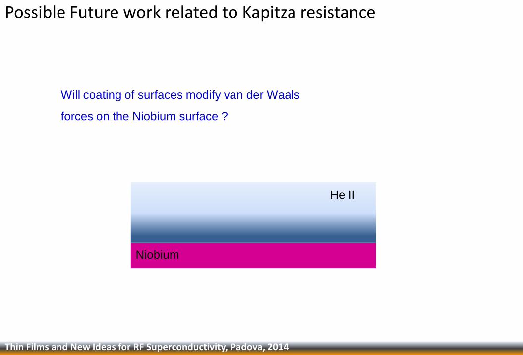
Possible Future work related to Kapitza resistance
Will coating of surfaces modify van der Waals
forces on the Niobium surface ?
Niobium
He II
Thin Films and New Ideas for RF Superconductivity, Padova, 2014

Thank you for your attention

Thin Films and New Ideas for RF Superconductivity, Padova, 2014
Nb +1 µm Ti
Nb after removal of 30µm
Nb after removal of 5 µm