jeol news vol 40.1
TRANSCRIPT
ISSN 1349-6832
July2005 Vol.40 No.1

Three-DimensionalReconstruction of BiologicalMacromolecular ComplexesUsing Cryoelectron Microscopyon Frozen-Hydrated Samples
Eric Larquet and Nicolas Boisset
Department of Structural Biology at the «Institut de Minéalogie et dePhysique des Milieux Condensés»
IntroductionObserving biological macromolecular com-
plexes in a frozen-hydrated state has been oneof the most exciting challenges of electronmicroscopy. Preserving biological moleculesin water and putting them into the high vacu-um of an electron microscope might look likea crazy idea, but when this water is frozen intoa vitreous state and when the electron dose iskept to a minimal amount (sufficient to createan image, but not strong enough to destroy thesample), this approach works beautifully.However, the low signal-to-noise ratio (SNR)generated in cryoelectron microscope imagesimposes a posteriori image processing, toretrieve the structural information on theobserved macromolecules. This necessity wasthe beginning of a strong partnership betweencryoEM and image processing in structuralbiology of macromolecular assemblies. Thepresent article is a short introduction to thisspecific field where intangible and transientbiological structures are observed with mini-mal electron doses and later processed to com-pute 3D averaged structures.
Preparation of BiologicalSamplesFreezing in vitreous ice
Beam damage was observed since earlydays on electron sensitive samples and biologi-cal specimens under the electron beam [2-6].The ideas of using higher voltage [7], lower
electron dose [8] and of freezing the specimen[9, 10] to prevent propagation of unstablechemical species were proposed successively.However, the spreading of cryoelectronmicroscopy occurred when vitreous ice wasobtained and observed in an electron micro-scope [11-13], and when biological objectssuch as a water suspension of viruses could beobserved [14]. For review see [15].
The easiest way to produce amorphous iceat normal atmospheric pressure is to make athin water layer (typically 60 to 100 nanome-ters), and to freeze it below -156°C as fast aspossible. The plunging apparatus shown inFig. 1 was designed by Marc Adrian to pre-pare vitreous ice, using liquid ethane as cryo-gen. Ethane is used here as the large gap( =94.7°C) between its melting (-183.45°C)and evaporating (-88.75°C) temperaturesallows the absorption of heat from the samplewithout formation of vapors. Indeed, evapora-tion prevents a good contact and a fast heatexchange with the sample (Leidenfrost effect).This is the case of liquid nitrogen which isused throughout the process to keep instru-ments and frozen samples cooled. At atmos-pheric pressure, liquid nitrogen has a verysmall gap ( =14.2°C) between its melting(-210.05°C) and evaporating (-195.85°C) tem-peratures, inducing a strong Leidenfrost effect.This explains why nitrogen cannot be usedunder normal atmospheric conditions as anefficient cryogen. As visible in Figs. 1b-d, asimple Styrofoam box partially filled with liq-uid ethane is used to create a cooling chamber,and the central metal cup is filled with liquidethane. In fact the metal cup has two cylindri-cal walls with a small gap in between, to slowdown the cooling from outer liquid nitrogen.Therefore, one has enough time to flow
Most regulation mechanisms of living organisms occur at molecular level throughlarge molecular assemblies. Such "molecular machines" are usually in the range of 10 to100 nanometers scale and their architecture can be studied by cryoelectron microscopy(cryoEM) in a frozen-hydrated state. This article gives a short introduction to this field ofstructural biology and describes some steps of image processing techniques used inconjunction with cryoEM. For a more complete introduction to 3D cryoEM and imageprocessing techniques we recommend the new edition of Joachim Frank's book [1].
I.M.P.M.C., UMR 7590 CNRS, UniversitiesP6, P7, and IPGP, 4 Place Jussieu, casepostale 115 - 75252 Paris cedex 05, FranceE-mail: [email protected]
Volume 40 Number 1July, 2005
Contents
Three-Dimensional Reconstruction ofBiological Macromolecular ComplexesUsing Cryoelectron Microscopy onFrozen-Hydrated Samples . . . . . . . . . . . 2
Direct Analysis in Real Time(DARTtm) Mass Spectrometry . . . . . . . 8
High Energy Backscattered Electron Imaging of SubsurfaceCu Interconnects . . . . . . . . . . . . . . . . . 13
Recent Development of TEMfor Advanced Ceramics. . . . . . . . . . . . 18
Advanced Analysis TechnologySupporting SiP . . . . . . . . . . . . . . . . . . 24
FT NMR New Technical Introduction. . 29● Introduction of Fully Automatic
NMR Measurement Tool"GORIN" for Protein Solution
● 100 Sample Auto Sample Changerand Tubeless NMR
● Windows Delta● Latest Information and Future for
ALICE2 SoftwareFeatures and Applications of
Newly-Developed GC-TOFMS"The AccuTOF GC" . . . . . . . . . . . . . .38
Development of Ion Slicer (Thin-FilmSpecimen Preparation Equipment) . . . 46
Introduction ofWafer Edge SEM Review. . . . . . . . . . . 50
Serving Advanced Technology
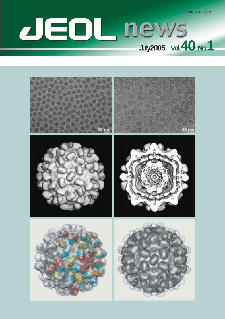
Cover micrographCryoEM applications to a swollen TomatoBushy Stunt Virus (TBSV). TEM images ofTBSV (taken with JEM-2100F with minimumdose system) and its 3D reconstructed struc-tures obtained using image processing tech-niques. (See pages 2 to 7)
Courtesy of Dr. Nicolas Boisset, Departmentof Structural Biology at the «Institut deMinéalogie et de Physique des MilieuxCondensés»
( 2) JEOL News Vol. 40 No.1 2 (2005)
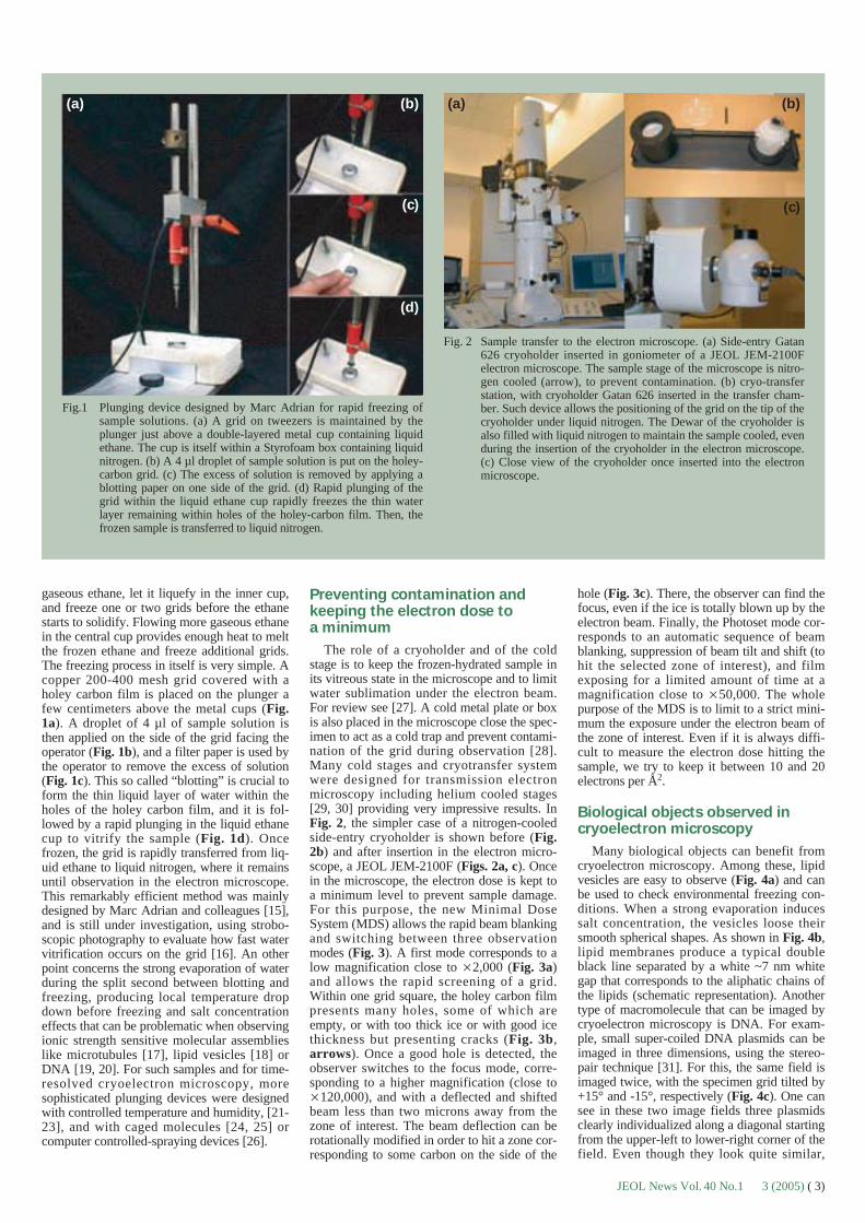
gaseous ethane, let it liquefy in the inner cup,and freeze one or two grids before the ethanestarts to solidify. Flowing more gaseous ethanein the central cup provides enough heat to meltthe frozen ethane and freeze additional grids.The freezing process in itself is very simple. Acopper 200-400 mesh grid covered with aholey carbon film is placed on the plunger afew centimeters above the metal cups (Fig.1a). A droplet of 4 µl of sample solution isthen applied on the side of the grid facing theoperator (Fig. 1b), and a filter paper is used bythe operator to remove the excess of solution(Fig. 1c). This so called “blotting” is crucial toform the thin liquid layer of water within theholes of the holey carbon film, and it is fol-lowed by a rapid plunging in the liquid ethanecup to vitrify the sample (Fig. 1d). Oncefrozen, the grid is rapidly transferred from liq-uid ethane to liquid nitrogen, where it remainsuntil observation in the electron microscope.This remarkably efficient method was mainlydesigned by Marc Adrian and colleagues [15],and is still under investigation, using strobo-scopic photography to evaluate how fast watervitrification occurs on the grid [16]. An otherpoint concerns the strong evaporation of waterduring the split second between blotting andfreezing, producing local temperature dropdown before freezing and salt concentrationeffects that can be problematic when observingionic strength sensitive molecular assemblieslike microtubules [17], lipid vesicles [18] orDNA [19, 20]. For such samples and for time-resolved cryoelectron microscopy, moresophisticated plunging devices were designedwith controlled temperature and humidity, [21-23], and with caged molecules [24, 25] orcomputer controlled-spraying devices [26].
Preventing contamination andkeeping the electron dose to a minimum
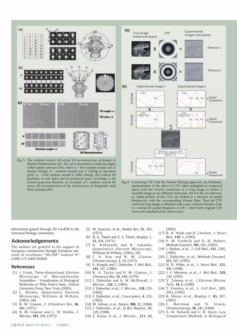
The role of a cryoholder and of the coldstage is to keep the frozen-hydrated sample inits vitreous state in the microscope and to limitwater sublimation under the electron beam.For review see [27]. A cold metal plate or boxis also placed in the microscope close the spec-imen to act as a cold trap and prevent contami-nation of the grid during observation [28].Many cold stages and cryotransfer systemwere designed for transmission electronmicroscopy including helium cooled stages[29, 30] providing very impressive results. InFig. 2, the simpler case of a nitrogen-cooledside-entry cryoholder is shown before (Fig.2b) and after insertion in the electron micro-scope, a JEOL JEM-2100F (Figs. 2a, c). Oncein the microscope, the electron dose is kept toa minimum level to prevent sample damage.For this purpose, the new Minimal DoseSystem (MDS) allows the rapid beam blankingand switching between three observationmodes (Fig. 3). A first mode corresponds to alow magnification close to �2,000 (Fig. 3a)and allows the rapid screening of a grid.Within one grid square, the holey carbon filmpresents many holes, some of which areempty, or with too thick ice or with good icethickness but presenting cracks (Fig. 3b,arrows). Once a good hole is detected, theobserver switches to the focus mode, corre-sponding to a higher magnification (close to�120,000), and with a deflected and shiftedbeam less than two microns away from thezone of interest. The beam deflection can berotationally modified in order to hit a zone cor-responding to some carbon on the side of the
hole (Fig. 3c). There, the observer can find thefocus, even if the ice is totally blown up by theelectron beam. Finally, the Photoset mode cor-responds to an automatic sequence of beamblanking, suppression of beam tilt and shift (tohit the selected zone of interest), and filmexposing for a limited amount of time at amagnification close to �50,000. The wholepurpose of the MDS is to limit to a strict mini-mum the exposure under the electron beam ofthe zone of interest. Even if it is always diffi-cult to measure the electron dose hitting thesample, we try to keep it between 10 and 20electrons per Å2.
Biological objects observed in cryoelectron microscopy
Many biological objects can benefit fromcryoelectron microscopy. Among these, lipidvesicles are easy to observe (Fig. 4a) and canbe used to check environmental freezing con-ditions. When a strong evaporation inducessalt concentration, the vesicles loose theirsmooth spherical shapes. As shown in Fig. 4b,lipid membranes produce a typical doubleblack line separated by a white ~7 nm whitegap that corresponds to the aliphatic chains ofthe lipids (schematic representation). Anothertype of macromolecule that can be imaged bycryoelectron microscopy is DNA. For exam-ple, small super-coiled DNA plasmids can beimaged in three dimensions, using the stereo-pair technique [31]. For this, the same field isimaged twice, with the specimen grid tilted by+15° and -15°, respectively (Fig. 4c). One cansee in these two image fields three plasmidsclearly individualized along a diagonal startingfrom the upper-left to lower-right corner of thefield. Even though they look quite similar,
Fig.1 Plunging device designed by Marc Adrian for rapid freezing ofsample solutions. (a) A grid on tweezers is maintained by theplunger just above a double-layered metal cup containing liquidethane. The cup is itself within a Styrofoam box containing liquidnitrogen. (b) A 4 µl droplet of sample solution is put on the holey-carbon grid. (c) The excess of solution is removed by applying ablotting paper on one side of the grid. (d) Rapid plunging of thegrid within the liquid ethane cup rapidly freezes the thin waterlayer remaining within holes of the holey-carbon film. Then, thefrozen sample is transferred to liquid nitrogen.
Fig. 2 Sample transfer to the electron microscope. (a) Side-entry Gatan626 cryoholder inserted in goniometer of a JEOL JEM-2100Felectron microscope. The sample stage of the microscope is nitro-gen cooled (arrow), to prevent contamination. (b) cryo-transferstation, with cryoholder Gatan 626 inserted in the transfer cham-ber. Such device allows the positioning of the grid on the tip of thecryoholder under liquid nitrogen. The Dewar of the cryoholder isalso filled with liquid nitrogen to maintain the sample cooled, evenduring the insertion of the cryoholder in the electron microscope.(c) Close view of the cryoholder once inserted into the electronmicroscope.
(a) (b) (a) (b)
(c)(c)
(d)
JEOL News Vol. 40 No.1 3 (2005) ( 3)

these two images contain enough informationto compute the outer shape of DNA in three-dimensions [32]. The three modeled DNA cir-cles appear in wire representation at the fore-front of Fig. 4c. Finally, large complexes suchas the Tobacco Mosaic Virus (TMV) are wide-ly used as test macromolecular assemblies forcryoelectron microscopy techniques. The 23 Åpitch of these helical structures are clearly visi-ble at the outer edges of the tubes (Fig. 4d)and produce a strong unmistakable layer linewhen imaging the power spectrum of suchimage. Therefore, TMV is often mixed insmall quantities within other biological samplepreparations, as it provides an internal refer-ence to accurately calibrate the magnificationof the microscope. Moreover, if TMV is poor-ly imaged in a given cryoEM grid, there is agood chance that other biological samples willbe even less visible. Therefore, getting repro-ducibly good images of TMV in vitreous ice isa good quality check when practicing cryo-electron microscopy. Finally, TMV is alsoused for testing new sample preparation tech-niques. For example, Fig. 4e shows a field ofTMV prepared with the cryonegative stainingtechnique designed by Marc Adrian [33]. Inthis technique, a saturated ammonium molyb-date solution is used as contrasting agent andmixed with the sample solution before blottingand plunging the grid into liquid ethane.Although, this technique rises some question-ing about respective contribution of amplitudeand phase contrasts involved in the image for-mation, it greatly enhances the contrast andallows the observation of small macromolecu-lar complexes (300 kDa and smaller), thatwould otherwise be difficult to see in vitreousice.
Image ProcessingCryoelectron microscopy of macromolecu-
lar complexes is often used in conjunction withimage processing. This grouping of techniquesresults from the low contrast (absence of heavymetal staining) and from the low signal-to-noise ratio (low electron dose) of cryoelectronmicroscope images. In fact, image processing,by computing 2D and 3D average maps from aseries of low dose images of similar complex-es, regains a strong signal to noise ratio with-out destroying biological samples with a high-er electron dose. The strategies of single parti-cle 3D reconstruction depend on the homo-geneity of the complexes, on their internalsymmetries, and on their ability to produce allpossible orientations within the vitreous icelayer. For review on image processing tech-niques see the new edition of Joachim Frank'sbook [1], the review of Marin van Heel [34],and two special issues of the Journal ofStructural Biology [35] and [36].
Strategies for single particles
There are numerous image processing soft-ware's devoted to single particle analysis, suchas IMAGIC [37], EMAN [38], XMIPP [39,40], FREALIGN [41] etc... It would be impos-sible to quote all of them here, and we there-fore restrict this section to the description ofone 3D reconstruction method called the “ran-dom conical tilt series” developed by MichaelRadermacher [42, 43] within the SPIDER soft-ware [44]. In this particular program, eachexperimental image is considered as the 2D
projection of a single object in a specific direc-tion characterized by a set of three Eulerianangles (Fig. 5a). Depending on software's,angular conventions change but the main idearemains the same. Once digitized and boxedinto a fixed frame, each experimental cryoEMimage of a single particle is characterized by aset of five parameters: (X-shift and Y-shift)necessary to center the particle within thedefined frame, and (three Eulerian angles , ,
) defining the direction of projection of theparticle in all possible orientations. Once thesefive parameters are known for a sufficientnumber of experimental images correspondingto as many different directions of projection, a3D map is computed. In Fig. 5b, the randomconical tilt series 3D reconstruction method isillustrated on a small phantom head. First, sev-eral copies of the phantom head are disposedin a “standing-up” orientation on a supportplane, and 2D projection images are producedwhen the support plane is tilted by 0° and 45°(Fig. 5b, left). A similar set of images isobtained in experimental conditions when thespecimen grid is tilted in the electron micro-scope. The 0° images are identical with eachother except for in-plane rotations, while 45°images correspond to a conical tilt series(Fig. 5b, middle). If one would try to visualizethe 3D Fourier transform of the phantom head,the conical tilt series would correspond to aseries of centered disks orthogonally orientedwith respect to their direction of projection(Fig. 5b, right). Figure 5c shows an applica-tion of this technique on a large respiratorypigment, the hemocyanin of the snail HelixPomatia [45]. In the upper part of Fig. 5c thesame specimen field is imaged twice with tiltangles of 45° and 0°, respectively. After digiti-zation, pairs of tilted- and untilted-specimenimages are interactively selected, using theWEB display program (white circles) [44]. Atthis stage the locations of particles in bothspecimen fields provide a mean for computingthe tilt angle ( ) and the in-plane direction oftilt axis ( ). A series of 0° and 45° image pairsis shown in Fig. 5c, lower-left part. While 45°images change according to a conical tiltgeometry, 0° images are all identical exceptfor an in-plane rotation corresponding to thelast Eulerian angle ( ). At this stage, after acentering procedure, the tilted-specimenimages are used to compute the 3D reconstruc-tion volume of the particle (Fig. 5c, lowerright).
Correcting the contrast transferfunction of the microscope
Dialogue between physicists and biologistsabout contrast transfer function (CTF) and itscorrection can be misleading. In fact thiscomes from the fact that we are not speakingof the same type of contrast and we are notusing the same defocus ranges. As most of thecontrast in a cryoEM images comes from thephase contrast, one has to make a compromisebetween defocus and visibility of isolated par-ticles in the ice layer. While in material sci-ences a reasonable defocus is close toScherzer, in cryoEM most people use defocusvalues 10 to 100 times bigger to produceenough contrast. The price to pay for this isthat the CTF oscillates far more and even inlow spatial frequencies. Figure 6 provides acrude description of the situation for a frozen-
hydrated sample, and the strategy used forCTF correction using the Wiener filteringapproach. More accurate descriptions andstrategies are available in [46-48].
While in real space one must consider thatthe true image of an object is convoluted bythe point spread function of the microscope, inreciprocal space, the Fourier transform of thetrue image is multiplied by the CTF. Sucheffect is represented in Figure 6a, where theFourier transformed true image of a little frogis multiplied in reciprocal space by a CTF cor-responding to a first low defocus and to a sec-ond stronger defocus. One can see that withthe first defocus the contrast is weak but smallstructural details are visible. Conversely, ahigher defocus provides a better overall con-trast but small structural details are blurred.
As shown at the top of Fig. 6b, the radialprofile of the CTF1 plotting the contrast as thefunction of spatial frequencies (defocus 1)oscillates less than the radial profile of CTF2(defocus 2). In these conditions, the experi-mental image obtained with defocus 2 crossesthe horizontal line (contrast equal to zero)three times, at spatial frequencies of 1/16Å-1,1/11Å-1, and 1/9Å-1. For these spatial frequen-cies the signal is lost and only noise remains.Therefore, Wiener filtering was proposed toselectively regain signal from experimentalimages and to mimic images produced by a“perfect instrument” (CTF equal to 1 for allspatial frequencies). Radial profiles of Wienerfilters 1 and 2 are designed to counterbalanceoscillations of CTF1 and CTF2, respectively.These filters are also designed to keep the con-trast low at spatial frequencies where contrastmainly comes from the noise. The CTF cor-rected average image obtained after Wienerfiltering and mixing of experimental images 1and 2 is shown in Fig. 6b. Even though thisimage resembles the true image of the object(Fig. 6a, right), there are still some local dif-ferences. This is understandable when lookingat the radial profile of the corrected CTF func-tion (Fig. 6b, lower right). Clearly this profileis not perfectly corrected for spatial frequency1/11Å-1. However, when looking at overlappedoriginal CTF profiles (Fig. 6b, lower left), itbecomes clear that at this spatial frequencyboth CTF are equal to zero and therefore bothimages only contained noise.
Impact of structural heterogeneity
The giant hemoglobin of the earth wormLumbricus terrestris is a good example ofmacromolecular complex with a high molecu-lar weight (~3 MDa). It consists of 144 globinchains packed into twelve dodecameric blocksby 36 linker chains. In the ice layer complexesare observed in all possible orientations (Fig.7a), and after alignment and sorting, three typ-ical top and side views (Fig. 7b) show thedodecameric units gathered in a hexagonalbilayer structure (Fig. 7c). The 3D reconstruc-tion volume was computed with a 14.9 Å reso-lution, using the Wiener filtering approach forCTF correction [49]. Such large respiratorypigments are easy to reconstruct as they arestructurally homogeneous. The few partiallydegraded complexes are easy to point out andto discard from the treatments. Conversely, forother complexes showing strong shape diversi-ty, it is almost impossible to compute a 3Dmap. However, image processing of such het-
( 4) JEOL News Vol. 40 No.1 4 (2005)

Fig. 4 Examples of biological macromolecular objects imaged by cryo-electron microscopy. (a) Lipid vesicles. (b) Visualization of thedouble layer of the lipid membrane as two parallel back lines sepa-rated by a white 7 nm spacing. (c) Stereo pairs of DNA circularplasmids. The same field is imaged twice with +15° and -15° tiltangles, allowing the 3D reconstruction of its outer contour (yellowwire models) [31, 32]. (d) Typical cryoelectron microscope viewof Tobacco Mosaic virus with its 23 Å pitch. (e) Similar TMVsample imaged by the cryo-negative staining technique of MarcAdrian, using a saturated solution of ammonium molybdate asstaining agent [33].
Fig. 3 Minimal dose system for recording cryoelectron microscopeimages. (a) Square grid of a holey carbon film observed at lowmagnification in “search” mode. (b) Enlarged detail of a portion ofimage (a) showing the ice layer within the holes of the carbonfilm. Holes showing defects (no ice, ice too thick, or ice withcracks) are not chosen, while other holes containing thin vitreousice are selected for photography. (c) MDS display. 100 nm
100 nm
(a)
(c)
(d)
(b)
(e)
erogeneous samples can still provide meaning-ful information. A good example is the case ofMalT, a transcriptional activator of the maltoseregulon in Escherichia coli. This (~100 kDa)transcriptional activators self-associates inelongated oligomers with the DNA maltoseregulon, in the presence of ATP and mal-totriose (Figs. 7d-e). Image processing high-lighted the significant conformational flexibili-ty of these polymeric forms and allowed us topropose a model of functional activation of thegene based on MalT binding to the target DNApromoters [50].
Impact of internal symmetries
Image processing strategies tend to useinternal symmetries of the particles to takeadvantage of signal redundancy during thecomputation of 3D volumes. Virus capsideswith helical and icosahedral symmetries repre-
sent particular cases and specific packageswere developed to take advantages of thererespective properties (for review on image pro-cessing packages see [35], and [36]). Anexample of icosahedral virus is the TomatoBushy Stunt Virus (TBSV) (Fig. 8) present incompact (Fig. 8a) and swollen (Fig. 8b) con-formations. When observing the 3D recon-struction volume of compact TBSV, the 180copies of the protein forming the capsid areclearly visible (Fig. 8c), while inner RNAwhich does not follow icosahedral symmetryproduces a non-descriptive spherical densitydistribution (Fig. 8d). Atomic coordinates ofcapsid protein [51] can be fitted on the com-pact cryoEM volume [34] (Fig. 8e), and theswelling process can be imaged by superpos-ing compact and swollen 3D reconstructionvolumes (Fig. 8f) and by hybrid approachusing combined experiments with small angleX-ray scattering [52].
Conclusion
Cryoelectron microscopy combined withimage processing is an efficient tool for struc-tural biology study of macromolecular assem-blies. For some highly homogeneous and sym-metrically redundant samples, resolutionsbelow 6Å are obtained [53-56]. However, formost single particles sub-nanometric resolu-tion is enough to fit alpha helices, and can beobtained using CCD cameras and automationof cryoEM observations [57, 58]. Presently,the European network “3D-EM” is promotingthe development of standard procedures forhigh resolution image processing. This net-work is also contributing through the work ofKim Henrick and E. B. I. (http://www.ebi.ac.uk/) to the development of the ElectronMicroscopy Data Base (http://www.ebi.ac.uk/msd/index.html) [59]. This bank will keepand make available the tremendous amount of
JEOL News Vol. 40 No.1 5 (2005) ( 5)
X
X =
=
True image(reciprocal space)
CTF ExperimentalImager (real space)
Defocus 1
Defocus 2
(a)
Fig. 6 Correcting CTF with the Wiener filtering approach: (a) Schematicrepresentation of the effect of CTF when multiplied in reciprocalspace with the Fourier transform of a frog image to mimic acryoEM image at two different defocuses. (b) For the two defocus-es, radial profiles of the CTFs are plotted as a function of spatialfrequencies, with the corresponding Wiener filter. Then the CTFcorrected Frog image is obtained with a new contrast function closeto 1 except for spatial frequency 1/11Å-1, where both original CTFcurves are simultaneously close to zero.
information gained through 3D cryoEM to thestructural biology community.
AcknowledgementsThe authors are grateful to the support ofEuropean commission through European net-work of excellence “3D-EM” contract N°LSHG-CT-2004-502828.
References
[1] J. Frank, Three-dimensional ElectronMicroscopy of MacromolecularAssemblies - Visualization of BiologicalMolecules in Their Native State., OxfordUniversity Press, New York, (2005),
[2] L. Reimer, Quantitative ElectronMicroscopy, Williams & Wilkins,(1965), 344
[3] R. M. Glaeser, J. Ultrastruct Res, 36,466, (1971)
[4] R. M. Glaeser and L. W. Hobbs, J.Microsc, 103, 209, (1975)
[5] M. Isaacson, et al., Radiat Res, 55, 205,(1973)
[6] R. E. Thach and S. S. Thach, Biophys J.,11, 204, (1971)
[7] K. Kobayashi and K. Sakaoku,Quantitative Electron Microscopy,Williams & Wilkins, (1965), 359
[8] I. A. Kuo and R. M. Glaeser,Ultramicroscopy, 1, 53, (1975)
[9] E. Knapek and J. Dubochet, J. Mol Biol.,141, 147, (1980)
[10] K. A. Taylor and R. M. Glaeser, J.Ultrastruct Res, 55, 448, (1976)
[11] J. Dubochet and A. W. McDowall, J.Microsc., 124, 3, (1981)
[12] J. Dubochet, et al., J. Microsc., 128, 219,(1982)
[13] J. Dubochet, et al., Cryo-Letters, 4, 233,(1983)
[14] M. Adrian, et al., Nature, 308, 32, (1984)[15] J. Dubochet, et al., Q Rev Biophys, 21,
129, (1988)[16] S. Kasas, et al., J. Microsc., 211, 48,
(2003)[17] R. H. Wade and D. Chretien, J. Struct
Biol., 110, 1, (1993)[18] P. M. Frederik and D. H. Hubert,
Methods Enzymol, 391, 431, (2005)[19] J. Bednar, et al., J. Cell Biol., 131, 1365,
(1995)[20] J. Dubochet, et al., Methods Enzymol,
211, 507, (1992)[21] H. D. White, et al., J. Struct Biol., 121,
306, (1998)[22] J. F. Menetret, et al., J. Mol Biol., 219,
139, (1991)[23] Y. Talmon, et al., J Electron Microsc
Tech., 14, 6, (1990)[24] T. Funatsu, et al., J. Cell Biol., 121,
1053, (1993)[25] K. Hirose, et al., Biophys J., 65, 397,
(1993)[26] J. Berriman and N. Unwin,
Ultramicroscopy, 56, 241, (1994)[27] A. W. Robards and U. B. Sleytr, Low
Temperature Methods in Biological
Fig. 5 The random conical tilt series 3D reconstruction technique ofMichael Radermacher [42, 43]. (a) Conventions of Eulerian angleswithin spider software [44], where = first rotation around axis Z(before tilting), = rotation around axis Y (tilting of specimengrid), = final rotation around Z (after tilting). (b) Conical tiltgeometry in real space and in reciprocal space according to thecentral projection theorem. (c) Example of a random conical tiltseries 3D reconstruction of the hemocyanin of Burgondy snailHelix pomatia [45].
1: 0 0 02: 0 45 03: 0 90 04: 0 90 905: -45 90 906: -90 90 907: -90 45 908: 0 0 90
( 6) JEOL News Vol. 40 No.1 6 (2005)
Fig. 7 Examples of single particles: (a) Giant hemoglobin from Lumbricus ter-restris observed in a JEOL JEM-2010F electron microscope at 200 kV,and under low electron dose conditions. (b) Selected 2D average maps ofhexagonal top views and rectangular bilayered side views. (c)Reconstruction volume at 14.9 Å resolution obtained after CTF correc-tion using the Wiener filtering approach [49]. (d) Oligomeric assembliesof MalT transcriptional activator complexed with DNA primers. (e)Average 2D map obtained from image processing and automatic classifi-cation of heterogeneous oligomeric forms.
a)
b)
c)
d) e)
30 nm
Electron Microscopy., Elsevier,Amsterdam, New York, Oxford., (1985),
[28] J. C. Homo, et al., J. Microsc., 136, 337.,(1984)
[29] F. Zemlin, et al., Science, 229, 461,(1985)
[30] Y. Fujiyoshi, Adv Biophys, 35, 25, (1998)[31] I. Dustin, et al., J. Struct Biol., 107, 15,
(1991)[32] E. Larquet, et al., J. Biomolec. Struct.
Dynamics, 12, a134, (1995)[33] M. Adrian, et al., Micron., 29, 145,
(1998)[34] M. van Heel, et al., Q Rev Biophys, 33,
307, (2000)[35] B. Carragher and P. R. Smith, J. Struct.
Biol., 116, 2, (1996)[36] B. Carragher and P. Penczek, J. Struct.
Biol., 144, 1, (2003)[37] M. van Heel, et al., J. Struct Biol., 116,
17, (1996)[38] S. J. Ludtke, et al., J. Struct Biol., 128,
82, (1999)
[39] C. O. Sorzano, et al., J. Struct Biol., 148,194, (2004)
[40] R. Marabini, et al., J. Struct Biol., 116,237, (1996)
[41] A. Stewart and N. Grigorieff,Ultramicroscopy, 102, 67, (2004)
[42] M. Radermacher, et al., J. Microsc., 146(Pt 2), 113, (1987)
[43] M. Radermacher, J. Electron MicroscTech, 9, 359, (1988)
[44] J. Frank, et al., J. Struct Biol., 116, 190,(1996)
[45] O. Lambert, et al., J. Mol Biol., 248, 431,(1995)
[46] Z. Huang, et al., J. Struct Biol., 144, 79,(2003)
[47] J. A. Velazquez-Muriel, et al.,Ultramicroscopy, 96, 17, (2003)
[48] S. J. Ludtke, et al., Structure (Camb), 12,1129, (2004)
[49] F. Mouche, et al., J. Struct Biol., 133,176, (2001)
[50] E. Larquet, et al., J. Mol Biol., 343, 1159,
(2004)[51] C. Chauvin, et al., J. Mol. Biol, 124, 641,
(1978)[52] R. Aramayo, et al., Biochim. Biophys.
Acta, (in press). (2005)[53] A. Miyazawa, et al., J. Mol Biol., 288,
765, (1999)[54] K. Yonekura, et al., Nature, 424, 643,
(2003)[55] F. A. Samatey, et al., Nature, 431, 1062,
(2004)[56] A. Fotin, et al., Nature, 432, 573, (2004)[57] B. Carragher, et al., J. Struct Biol., 132,
33, (2000)[58] C. R. Booth, et al., J. Struct Biol., 147,
116, (2004)[59] K. Henrick, et al., J. Struct Biol., 144,
228, (2003)
Fig. 8 The swelling of Tomato Bushy Stunt Virus (TBSV): (a) TBSV in itscompact conformation observed on a JEOL JEM-2010F with anacceleration voltage of 200 kV with the MDS system. (b) TBSV inits swollen conformation after pH modification from 6.5 to 7.4 andcalcium removal using EDTA as chelating agent. (c) Reconstructionvolume of compact TBSV at 13 Å resolution. (d) Same volume as(c) but after removing the front half to see inner features and RNAradial location. (e) Fitting of atomic structures of capsid proteins onthe 3D cryoEM maps. (f) Surface rendering of the compact (darkgrey) and the swollen (semi-transparent) TBSV 3D cryoEM maps.
a)
c)
e)
b)
d)
f)
15 nm
JEOL News Vol. 40 No.1 7 (2005) ( 7)

Direct Analysis in Real Time (DARTtm) MassSpectrometry
Introduction
Mass Spectrometry (MS) is one of thefastest-growing areas in analytical instrumen-tation. The use of mass spectrometry in sup-port of synthetic, organic, and pharmaceuticalchemistry is well established. Mass spectrome-try is also used in materials science, environ-mental research, and forensic chemistry. It hasalso evolved into one of the core methods usedin biotechnology. However, currently avail-able ion sources place extreme restrictions onthe speed and convenience of sample analysisby mass spectrometry. Here we report amethod for using mass spectrometry to instan-taneously analyze gases, liquids, and solids inopen air at ground potential under ambientconditions.
Traditional ion sources used in mass spec-trometry require the introduction of samplesinto a high vacuum system. Traditional ionsources operated in vacuum include electronionization (EI)[1], chemical ionization (CI)[2],fast atom bombardment (FAB)[3], and fielddesorption/field ionization (FD/FI)[4]. Thesetechniques have been used successfully fordecades. However, the requirement that sam-ples be introduced into a high vacuum foranalysis is a severe limitation. Gas or liquidsamples must be introduced through a gaschromatograph or a specially designed inletsystem. Solid samples must be introduced byusing a direct insertion probe and a vacuumlock system. Direct insertion probes can resultin vacuum failure and/or contamination of the
ion source if too much sample is introduced. Atmospheric pressure ion sources such as
atmospheric pressure chemical ionization(APCI)[5], electrospray ionization (ESI)[6-8],matrix-assisted laser desorption ionization(MALDI)[9-10] and atmospheric pressurephotoionization (APPI)[11] have broadenedthe range of compounds that can be analyzedby mass spectrometry. However, these ionsources require that samples be exposed to ele-vated temperatures and electrical potentials,ultraviolet irradiation, laser radiation, or ahigh-velocity gas stream. Safety considera-tions require that the ion source be fullyenclosed to protect the operator from harm.
The new ion source reported herein over-comes these limitations. The new technique,referred to as Direct Analysis in Real Time(DARTtm), has been coupled to the AccuTOF-LCtm atmospheric pressure ionization massspectrometer to permit high-resolution, exactmass measurements of gases, liquids, andsolids[12,13]. DART successfully sampledhundreds of chemicals, including chemicalagents and their signatures, pharmaceutics,metabolites, pesticides and environmentallysignificant compounds, peptides and oligosac-charides, synthetic organics, organometallics,drugs of abuse, explosives, and toxic industrialchemicals. These chemicals were detected on avariety of surfaces such as concrete, humanskin, currency, airline boarding passes, fruitsand vegetables, body fluids, cocktail glasses,and clothing. The composition of drug cap-sules and tablets was directly analyzed.
Background and Principle ofOperation
DART grew out of discussions at JEOLUSA, Inc. between two of the authors(Laramee and Cody) about the possibility ofdeveloping an atmospheric pressure thermalelectron source to replace the radioactive
sources used in hand-held detectors for chemi-cal weapons agents (CWAs), drugs, and explo-sives. The discovery that DART could beused for positive-ion and negative-ion non-contact detection of materials on surfaces, aswell as for detection of gases and liquids, ledto the development of a commercial product.
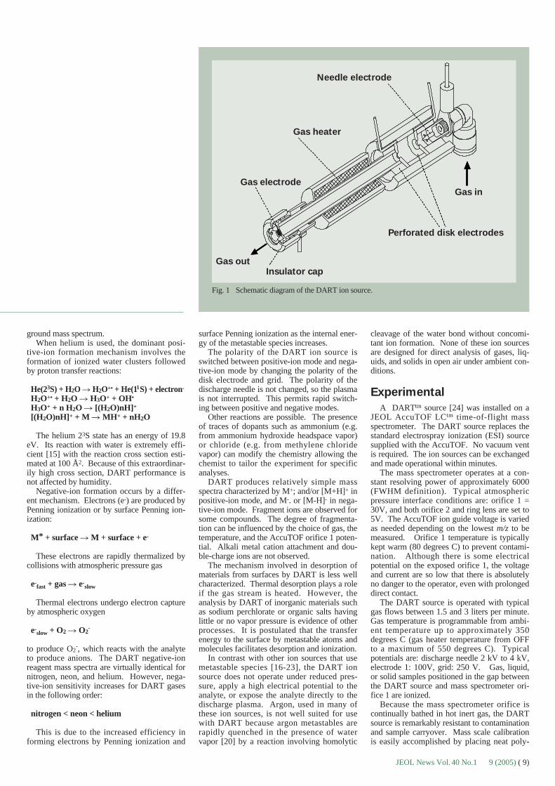
DART is based on the atmospheric pressureinteractions of long-lived electronic excited-state atoms or vibronic excited-state moleculeswith the sample and atmospheric gases. TheDART ion source is shown in Figure 1. A gas(typically helium or nitrogen) flows through achamber where an electrical discharge pro-duces ions, electrons, and excited-state(metastable) atoms and molecules. Most ofthe charged particles are removed as the gaspasses through perforated lenses or grids andonly the neutral gas molecules, includingmetastable species, remain. A perforated lensor grid at the exit of the DART provides sever-al functions: it prevents ion-ion and ion-elec-tron recombination, it acts as a source of elec-trons by surface Penning ionization, and it actsas an electrode to promote ion drift toward theorifice of the mass spectrometer’s atmosphericpressure interface.
Several ionization mechanisms are possible,depending on the polarity and reaction gas, theproton affinity and ionization potential of theanalyte, and the presence of additives ordopants. The simplest process is Penning ion-ization [14] involving transfer of energy fromthe excited gas M* to an analyte S having anionization potential lower than the energy ofM*. This produces a radical molecular cationS+• and an electron (e-).
M* + S � S+• + M + electron-
Penning ionization is a dominant reactionmechanism when nitrogen or neon is used inthe DART source. Nitrogen or neon ions areeffectively removed by the electrostatic lensesand are never observed in the DART back-
Robert B. Cody†, James A. Laramée††,J. Michael Nilles†††, and H. Dupont Durst††††
†JEOL USA, Inc.††EAI Corporation
†††Geo-Centers Inc. ††††Edgewood Chemical Biological Center
†11 Dearborn Road, Peabody, Massachusetts,USA.
††1308 Continental Drive, Suite J, Abingdon,MD 21009
†††Box 68 Gunpowder Branch, APG, MD21010
††††Aberdeen Proving Grounds, MarylandUSA
( 8) JEOL News Vol.40 No.1 8 (2005)
ground mass spectrum.When helium is used, the dominant posi-
tive-ion formation mechanism involves theformation of ionized water clusters followedby proton transfer reactions:
He(23S) + H2O � H2O+• + He(11S) + electron-
H2O+• + H2O � H3O+ + OH•
H3O+ + n H2O � [(H2O)nH]+
[(H2O)nH]+ + M � MH+ + nH2O
The helium 23S state has an energy of 19.8eV. Its reaction with water is extremely effi-cient [15] with the reaction cross section esti-mated at 100 Å2. Because of this extraordinar-ily high cross section, DART performance isnot affected by humidity.
Negative-ion formation occurs by a differ-ent mechanism. Electrons (e-) are produced byPenning ionization or by surface Penning ion-ization:
M* + surface � M + surface + e-
These electrons are rapidly thermalized bycollisions with atmospheric pressure gas
e-fast + gas � e-
slow
Thermal electrons undergo electron captureby atmospheric oxygen
e-slow + O2 � O2
-
to produce O2-, which reacts with the analyte
to produce anions. The DART negative-ionreagent mass spectra are virtually identical fornitrogen, neon, and helium. However, nega-tive-ion sensitivity increases for DART gasesin the following order:
nitrogen < neon < helium
This is due to the increased efficiency informing electrons by Penning ionization and
surface Penning ionization as the internal ener-gy of the metastable species increases.
The polarity of the DART ion source isswitched between positive-ion mode and nega-tive-ion mode by changing the polarity of thedisk electrode and grid. The polarity of thedischarge needle is not changed, so the plasmais not interrupted. This permits rapid switch-ing between positive and negative modes.
Other reactions are possible. The presenceof traces of dopants such as ammonium (e.g.from ammonium hydroxide headspace vapor)or chloride (e.g. from methylene chloridevapor) can modify the chemistry allowing thechemist to tailor the experiment for specificanalyses.
DART produces relatively simple massspectra characterized by M+; and/or [M+H]+ inpositive-ion mode, and M-. or [M-H]- in nega-tive-ion mode. Fragment ions are observed forsome compounds. The degree of fragmenta-tion can be influenced by the choice of gas, thetemperature, and the AccuTOF orifice 1 poten-tial. Alkali metal cation attachment and dou-ble-charge ions are not observed.
The mechanism involved in desorption ofmaterials from surfaces by DART is less wellcharacterized. Thermal desorption plays a roleif the gas stream is heated. However, theanalysis by DART of inorganic materials suchas sodium perchlorate or organic salts havinglittle or no vapor pressure is evidence of otherprocesses. It is postulated that the transferenergy to the surface by metastable atoms andmolecules facilitates desorption and ionization.
In contrast with other ion sources that usemetastable species [16-23], the DART ionsource does not operate under reduced pres-sure, apply a high electrical potential to theanalyte, or expose the analyte directly to thedischarge plasma. Argon, used in many ofthese ion sources, is not well suited for usewith DART because argon metastables arerapidly quenched in the presence of watervapor [20] by a reaction involving homolytic
cleavage of the water bond without concomi-tant ion formation. None of these ion sourcesare designed for direct analysis of gases, liq-uids, and solids in open air under ambient con-ditions.
Experimental
A DARTtm source [24] was installed on aJEOL AccuTOF LCtm time-of-flight massspectrometer. The DART source replaces thestandard electrospray ionization (ESI) sourcesupplied with the AccuTOF. No vacuum ventis required. The ion sources can be exchangedand made operational within minutes.
The mass spectrometer operates at a con-stant resolving power of approximately 6000(FWHM definition). Typical atmosphericpressure interface conditions are: orifice 1 =30V, and both orifice 2 and ring lens are set to5V. The AccuTOF ion guide voltage is variedas needed depending on the lowest m/z to bemeasured. Orifice 1 temperature is typicallykept warm (80 degrees C) to prevent contami-nation. Although there is some electricalpotential on the exposed orifice 1, the voltageand current are so low that there is absolutelyno danger to the operator, even with prolongeddirect contact.
The DART source is operated with typicalgas flows between 1.5 and 3 liters per minute.Gas temperature is programmable from ambi-ent temperature up to approximately 350degrees C (gas heater temperature from OFFto a maximum of 550 degrees C). Typicalpotentials are: discharge needle 2 kV to 4 kV,electrode 1: 100V, grid: 250 V. Gas, liquid,or solid samples positioned in the gap betweenthe DART source and mass spectrometer ori-fice 1 are ionized.
Because the mass spectrometer orifice iscontinually bathed in hot inert gas, the DARTsource is remarkably resistant to contaminationand sample carryover. Mass scale calibrationis easily accomplished by placing neat poly-
Fig. 1 Schematic diagram of the DART ion source.
Gas heater
Gas electrode
Insulator capGas out
Needle electrode
Gas in
Perforated disk electrodes
JEOL News Vol. 40 No.1 9 (2005) ( 9)
ethylene glycol average molecular weight 600(PEG 600) on a glass rod or a piece ofabsorbent paper in front of the DART source.In positive-ion mode, this produces a series of[M+H]+ and [M+H-H2O]+ peaks from m/z 45up to beyond m/z 1000. By including back-ground peaks, the calibrated mass range can beextended down to m/z 18 or 19. Negative-ionspectra of PEG are characterized by [M+O2-H]- and [(C2H4O)n+O2-H]- ion series.
The reference spectrum can be acquiredwithin seconds. There is no memory effect orcarryover of the reference compound -- thePEG peaks do not persist after the referencestandard is removed. For these reasons, a fullreference mass spectrum can be quickly andeasily included in each data file, and accuratemass measurements are routinely acquired forall samples.
Applications
The DART ion source has been used to ana-lyze an extremely wide range of analytes,including drugs (prescription, over-the-count-er, veterinary, illicit, and counterfeit) in doseform or in body fluids or tissues, explosivesand arson accelerants, chemical weaponsagents and their signatures, synthetic organicor organometallics compounds, environmen-tally important compounds, inks and dyes,foods, spices and beverages. An importantbenefit of DART is that materials can be ana-lyzed directly on surfaces such as glass, TLCplates, concrete, paper, or currency withoutrequiring wipes or solvent extraction.
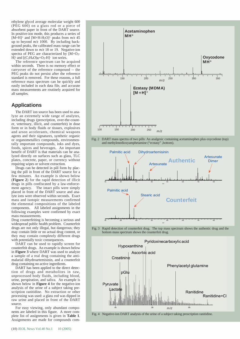
Drugs can be detected in pill form by plac-ing the pill in front of the DART source for afew minutes. An example is shown below(Figure 2) for the rapid detection of illicitdrugs in pills confiscated by a law-enforce-ment agency. The intact pills were simplyplaced in front of the DART source and ana-lyte ions were observed within seconds. Exactmass and isotopic measurements confirmedthe elemental compositions of the labeledcomponents. All labeled assignments in thefollowing examples were confirmed by exactmass measurements. Drug counterfeiting is becoming a serious andwidespread public health problem. Counterfeitdrugs are not only illegal, but dangerous; theymay contain little or no actual drug content, orthey may contain completely different drugswith potentially toxic consequences.
DART can be used to rapidly screen forcounterfeit drugs. An example is shown belowin Figure 3 where DART was used to analyzea sample of a real drug containing the anti-malarial dihydroartemisinin, and a counterfeitdrug containing no active ingredients.
DART has been applied to the direct detec-tion of drugs and metabolites in raw,unprocessed body fluids, including blood,urine, perspiration, and saliva. An example isshown below in Figure 4 for the negative-ionanalysis of the urine of a subject taking pre-scription ranitidine. No extraction or otherprocessing was used: a glass rod was dipped inraw urine and placed in front of the DARTsource.
For easy viewing, only abundant compo-nents are labeled in this figure. A more com-plete list of assignments is given in Table 1.Assignments are made for compounds com-
Fig. 2 DART mass spectra of two pills: An analgesic containing acetaminophen plus oxycodone (top)and methylenedioxyamphetamine (“ecstasy” ,bottom).
Fig. 3 Rapid detection of counterfeit drug. The top mass spectrum shows the authentic drug and thebottom mass spectrum shows the counterfeit drug.
Fig. 4 Negative-ion DART analysis of the urine of a subject taking prescription ranitidine.
m/z
150 200 250 300 350m/z
150 200 250 m/z100
Ecstasy (MDMA)[M�H]�
AcetaminophenMH�
OxycodoneMH�
Counterfeit
Authentic
(10) JEOL News Vol.40 No.1 10 (2005)

monly encountered in urine that have elemen-tal compositions that match the measured m/zvalues. It is interesting to note that the basicdrug, ranitidine, is observed as an [M-H]-species in the negative-ion mass spectrum aswell as an abundant [M+H]+ species in thepositive-ion mass spectrum. Ranitidinemetabolites are also observed [11] in the posi-tive-ion mass spectrum (not shown).
DART can be used for quantitative analysis.The absolute abundance of ions produced byDART depends on the positioning of the targetin the gas stream. However, the use of aninternal standard permits rapid quantitativeanalysis of drugs in urine, plasma, or otherbody fluids. Figure 5 shows a working curveobtained for urine samples spiked with pro-mazine at the 1 to 500 ppm level.Chlorpromazine (50 ppm) was added as aninternal standard. Undiluted urine sampleswere applied to a glass rod. Each analysis wascomplete within seconds of placing the rod infront of the DART source. This approach hasalso been used to screen for the “date rape”drug gamma hydroxy butyrate (GHB) in urine[24] and for the rapid quantitative analysis ofdevelopmental drugs in plasma.
The detection of explosives is important forforensics and security. DART has beenapplied to the detection of nitro explosivessuch as nitroglycerine, TNT, and HMX, inor-ganic explosives such as ammonium nitrate,perchlorate and azide, and peroxide explosivessuch as TATP and HMTD. Examples areshown in Figures 6 and 7.
The high dynamic range of the DART-AccuTOF combination can permit the identifi-cation of trace-level impurities for quality con-trol and similar applications. An example isshown in Figure 8 and Table 2 for the exact-mass analysis of 1% propazine and 0.2%simazine in a sample of the herbicide atrazine.
Conclusion
A new ion source has been developed thatpermits the analysis of gases, liquids, andsolids in open air under ambient conditions.No solvents or high-pressure gases are used.The sample is not directly exposed to highvoltages, laser beams or radiation or plasma.The combination of this source with a high-resolution time-of-flight mass spectrometerpermits rapid qualitative and quantitativeanalysis of a wide variety of materials.
Acknowledgment
Technical assistance and keen scientificinsight were unselfishly provided by (in alpha-betical order) Daniel Banquer, Ted Boileau,William Creasy, Daniel Evans, DrewMcCrady, Michael McKie, Michael Nilles,Edward Owen, Gary Samuelson, Philip Smith,John Stuff, and Dean Tipple. The authorswould like to thank Prof. Facundo Fernandezof Georgia Tech University for the dihy-droartemisinin and counterfeit drug sample.
Additional Information
Additional applications and digital videosshowing DART analysis are available on theinternet at http://www.jeolusa.com/ms/msprod-
Name Meas. Calc. Diff(u) Abund.GBL 85.0295 85.0290 0.0006 11.0317Pyruvic_acid 87.0084 87.0082 0.0002 7.1700Lactic_acid 89.0236 89.0239 -0.0002 8.3658Cresol 107.0492 107.0497 -0.0004 .9294Uracil 111.0153 111.0195 -0.0041 14.3328Creatinine 112.0513 112.0511 0.0002 81.6851Purine 119.0354 119.0358 -0.0004 31.9510Niacin 122.0277 122.0242 0.0035 3.1489Dihydro_methyluracil 127.0486 127.0508 -0.0021 23.3773pGlu 128.0353 128.0348 0.0006 59.2337Methylmaleic_acid 129.0212 129.0188 0.0024 37.1191Me_succinate/diMe_malonate 131.0368 131.0358 0.0010 19.3593Deoxyribose 133.0489 133.0501 -0.0012 28.3521Hypoxanthine 135.0306 135.0307 -0.0001 100.0000Adipic_acid 145.0469 145.0501 -0.0032 11.7389Methyl_hypoxanthine 149.0454 149.0463 -0.0009 37.5243Hydroxymethyl_methyl_uracil 155.0453 155.0457 -0.0003 55.5832a-aminoadipic_acid 160.0568 160.0610 -0.0042 9.5885Methionine_sulfoxide 164.0419 164.0381 0.0037 11.7609Methylxanthine 165.0408 165.0412 -0.0004 32.4341Formiminoglutamic_acid 173.0536 173.0562 -0.0027 12.3531Ascorbic_acid 175.0285 175.0243 0.0042 23.1998Hippuric_acid 178.0513 178.0504 0.0009 66.4487Glucose 179.0552 179.0556 -0.0004 39.7499Dimethylxanthine 179.0552 179.0569 -0.0017 39.7499Pyridoxinecarboxylic_acid 182.0479 182.0453 0.0026 34.7913Hydroxyindoleacetic_acid 190.0542 190.0504 0.0037 5.4133Dimethyluric_acid 195.0527 195.0518 0.0009 23.7577AAMU (caffeine metabolite) 197.0667 197.0675 -0.0007 79.6617Cinnamalidinemalonic_acid 217.0483 217.0501 -0.0017 60.5399AFMU (caffeine metabolite) 225.0643 225.0624 0.0019 21.9092Cytidine 242.0801 242.0777 0.0024 3.4545Uridine 243.0641 243.0617 0.0024 21.1156Phenylacetyl_glutamine 263.1033 263.1032 0.0001 48.9665Adenosine 266.0861 266.0889 -0.0028 1.4869Ranitidine 313.1321 313.1334 -0.0013 8.7459Ranitidine+Cl 349.1113 349.1101 0.0011 11.7296
Table 1 Assignments for Compounds Detected in Negative-Ion DART Mass Spectrum of Raw Urine.
Fig. 5 Rapid quantitative analysis by DART of promazine in urine. Chlorpromazine was added as aninternal standard.
JEOL News Vol. 40 No.1 11 (2005) (11)

saccutof_dart.html. Chemical agent data isavailable from the authors upon request.
References
[1] Dempster, A. J. Phys. Rev., 11, 316-324,(1918).
[2] Munson, M. S. B.; Franklin, F. H. J. Am.Chem. Soc., 88, 2621, (1966).
[3] Barber, M.; Bordoli, R. S.; Elliott, G. J.;Sedgwick, R. D.; Tyler, A. N. J. Chem.Soc. Chem. Commun., 325, (1981).
[4] Beckey H. D. Research/Development,20(11), 26-29, (1969).
[5] Horning, E. C.; Horning, M. E.; Carroll,D. I.; Dzidic, I.; Stilwell, R. N.; Anal.Chem., 45, 936-943, (1973).
[6] Dole, M. Mack, L. L. Hines, R. L.;Mobley, R. C.; Ferguson, L. D. Alice, M.A. J. Chem. Phys., 49, 2240, (1968).
[7] Aleksandrov, M. L.; Gall, L. N. Krasnov,N. V. Nikolaev, V. I. Pavlenko, V. A.;Shkurov, V. A. Dokl. Akad. Nauk. SSSR,277, 379-383, (1984).
[ 8] Fenn, J. B.; Mann, M.; Meng, C. K.;Wong, S. F. Science, 246, 64-71, (1989).
[9] Tanaka, K.; Waki, H.; Ido, Y; Akita, S.;Yoshida, Y. Rapid. Commun. MassSpectrom., 2, 151-153, (1988).
[10] Karas, M.; Hillenkamp, F. Anal. Chem.,60, 2299-2301, (1988).
[11] Robb, D. B.; Covey, T. R.; Bruins, A. P.Anal. Chem., 72, 3653-3659, ( 2000).
[12] Cody, R. B.;Laramee, J. A. ; Durst, H. D.Anal. Chem., 77(8), 2297 – 2302, (2005).
[13] Patents pending.[14] Penning, F. M. Naturwissenschaften, 15,
818, (1927).[15] Mastwijk, H. C. Cold Collisions of
Metastable Helium Atoms, Ph.D. Thesis,University of Utrecht, Netherlands,(1997).
[16] Faubert, D.; Paul, G.J.C., Giroux, J.;Bertrand, M. J. Int. J. Mass Spectrom. IonProc., 124, 69, (1993).
[17] Faubert, D.; L’Heureux, A.; Peraldi, O.;Mousselmal, M.; Sanchez, G.; Bertrand,M. J.; “Metastable Atom Bombardment(MAB) Ionization Source: Design,Optimization and AnalyticalPerformances” in Adv. Mass Spectrom.:15th International Mass SpectrometryConference, Wiley: Chichester, UK, 431-432, (2001).
[18] http://www.jeol.com/ms/docs/map_note.pdf.
[19] Tsuchiya, M. Kuwabara, H.; Anal. Chem.,56, 14, (1984).
[20] Tsuchiya, M. Mass Spectrom. Rev., 17,51, (1998).
[21] Tsuchiya, M. Analytical Sciences,, 14,661-676, (1998).
[22] Hiraoka, K.; Fujimaki, S.; Kambara, S.;Furuya, H.; Okazaki, S. Rapid Commun.Mass Spectrom., 18, 2323-2330, (2004).
[23] McLuckey, S. A.; Glish, G. L.; Asano, K.G.; Grant, B. C., Anal. Chem., 60, 2220, (1988).
[24] Guzowski, J. P., Jr.; Broekaert, J. A. C.;Ray, S. J.; Hieftje, G. M. J. Anal. At.Spectrom., 14, 1121-1127, (1999).
[25] IonSense, Inc., 11 Dearborn Road,Peabody, MA USA 01960.
[26] Jagerdeo, E.; Cody, R. B. unpublishedresults.
Fig. 6 3 ppm explosives spiked into muddy water. 1=DNT, 2=amino-DNT, 3=trinitrobenzene,4=TNT, 5=RDX+TFA, 6=Tetryl, 7=HMX+TFA, 8=palmitate in the water background(used as lock mass). Headspace vapor from a 0.1% aqueous solution of trifluoroaceticacid was used to produce TFA adducts.
Fig. 7 Positive-ion DART mass spectrum of triacetone triperoxide (TATP). Ammonium hydrox-ide headspace vapor provided a source of NH4
+.
Fig. 8 Exact-mass analysis of trace simazine and propazine in a sample of the herbicide atrazine.
Table 2 DART measured masses for [M+H]+ from atrazine and trace impurities.
Compound Composition Measured Calculated Diff. (mmu)
Atrazine C8H15N5Cl 216.10159 216.10160 �0.01
Propazine C9H17N5C 230.11760 230.11725 �0.35
Simazine C7H13N5Cl 202.08440 202.08595 �1.60
61
8
150 400
4
2
3 5 7
200 250 300 350
m/z
150 200100
m/z
(12) JEOL News Vol.40 No.1 12 (2005)
High Energy Backscattered Electron Imaging ofSubsurface Cu Interconnects
Lynne M. Gignac†, Masahiro Kawasaki††, Steven H. Boettcher††† andOliver C. Wells††††
†IBM T. J. Watson Research Center††JEOL USA, Inc. †††IBM Microelectronics Division††††IBM T. J. Watson Research Center, Emeritus
Introduction
The scanning electron microscope (SEM) isa critical tool for in-line defect characteriza-tion, critical dimension measurements and fail-ure analysis of semiconductor devices. Asdevices continue to shrink, the trend in imag-ing fine semiconductor structures in the SEMhas been to use field emission electron sourcesat low beam energies, < 5 keV, and to detectsecondary electrons (SE). This small spot, lowbeam current configuration can produce highresolution images of the sample surface withminimal sample charging. However, whenhigher energy incident electron beams areemployed and backscattered electrons (BSEs)are detected, images can be obtained with hightopographic or atomic number (Z) contrast anddetail below the sample surface can be detect-ed [1-5]. A specific application for BSE sub-surface imaging is for the characterization ofmulti-level Cu interconnects passivated withSiO2 or low dielectric constant amorphousdielectrics [6-22]. Here the low Z surfacedielectric does not greatly scatter the electronbeam allowing the higher Z, Cu-Ta containingsubsurface lines to be imaged with BSEs.Defects such as voids in Cu interconnects ormetal extruded out of the interconnect can beimaged with one, topdown BSE image, even ifthe defect is buried under complex, dielectricsurface topography or upper level metal. BSEimaging has potential as a technique that isable to characterize subsurface device struc-
tures without having to physically alter thesample by cross-sectioning or delayeringthough electron beam induced damage ofdevices has been reported [11-12].
Initial work on BSE subsurface imaging ofinterconnect structures was published in the1990’s where both SEMs [6-8, 10-15] andtransmission electron microscopes (TEMs)with scanning attachments [6, 9, 17] were usedto image Al interconnects passivated with SiO2
or SiNx. Since the image resolution wasdependent on the beam spread caused by scat-tering by sample atoms, higher energy incidentelectron beams were used to reduce beambroadening and to improve the resolution ofthe BSE images.
Energy filtered BSE imaging has been stud-ied as a microtomography technique where aseries of images representing specific BSEenergies were collected for a given incidentelectron beam energy [13-15]. Since BSEswhich have lost a certain amount of energy aretypically generated from a given depth in thesample, an energy-filtered image series repre-sents two-dimensional slices of the sample atvarious points below the sample surface.Since interconnects are non-uniform in com-position laterally, an energy-filtered image cansuffer from contrast inversion where a lowatomic number layer that is located deep belowthe surface can have higher intensity than ahigh atomic number layer located closer to thesurface. Therefore, a given BSE energy imagewill represent a variety of depths below thesurface making the microtomography recon-struction difficult.
In recent years, there has been renewedinterest in using BSE to image subsurface
interconnect structures [18-21]. In this paper,subsurface imaging of multi-level Cu intercon-nects with BSEs is demonstrated by usingtransmission electron microscopes with scan-ning attachments with beam energies of 150keV to 400 keV. The BSE images were usedto detect voids in subsurface Cu interconnectsand to characterize beam spread at variousdepths below the surface.
Experimental Procedure
High voltage BSE imaging of bulk, passi-vated Cu-SiO2-SiNx interconnects was per-formed at 150 keV and 400 keV using a JEOLJEM-4000FX TEM with a LaB6 thermionicsource and at 300 keV in a JEOL JEM-3000FTEM with a Schottky field emission source.Both TEMs were equipped with scanningattachments and BSE detectors. The JEM-4000FX had a rectangular shaped, 2-piece Sisolid state BSE detector located under theobjective polepiece, 4 mm above the samplesurface with a hole in the center to allow pas-sage of the electron beam. The detector solidangle was ~1.3 sr and it detected electronsbackscattered at angles of 27-54° from theincident beam direction. The JEM-3000F hada microchannel plate (MCP), annular shaped,center hole detector located above the objec-tive polepiece, 46 mm above the sample sur-face. The detector solid angle was ~0.14 srand detected BSE at angles of 3-12° from theincident beam direction. The MCP detectorcould be biased allowing the detection ofeither BSEs or SEs. In addition to the solidstate BSE detector, the JEM-4000FX had anEverhart-Thornley SE detector.
1101 Kitchawan Road, Route 134, YorktownHeights, N. Y. 10598Email: [email protected]
In bulk Si integrated circuit devices, passivated copper interconnects that were located 0.65-2.7 µm below thesurface were imaged in two different transmission electron microscopes with scanning attachments by detectingbackscattered electrons (BSEs) using incident beam energies that ranged from 150 keV to 400 keV. Since the BSEyield was strongly dependent on atomic number, voids in the subsurface Cu interconnects could be detected with-out having to alter the sample by cross-sectioning or delayering even when the voids were located under complex,dielectric surface topography or upper level Cu lines or vias. Because the electron beam broadens from low angle,elastic scattering events during the initial stages of penetration into the sample, the subsurface image resolutiondepended on the depth below the surface where the electrons were backscattered, the composition of the over-layer material(s) and the incident beam energy. Beam spreads were measured at several incident beam energiesfrom BSE images of Cu interconnects buried under varying thicknesses of SiO2-SiNx dielectric. Tilt series tomogra-phy was attempted on passivated, 2-level Cu interconnects but increased beam spread and decreased signal withtilt allowed imaging up to only ±40°.
JEOL News Vol. 40 No.1 13 (2005) (13)

Bulk samples could be inserted in bothmicroscopes using standard sample holders ifthey were cored into 3 mm discs and backsidepolished to reduce the sample thickness. In theJEM-4000FX, a bulk specimen holder wasalso available and could be used to study chipsthat had dimensions less than 4 � 8 mm. Inboth microscopes, electronic BSE imagescould be acquired using digital image capturesystems.
Free lens control was used to create highercurrent probes than the standard probes usedfor scanning transmission electron microscope(STEM) bright field or dark field imaging ofthin samples. The high current conditionswere produced by weakening the first con-denser lens strength so that a larger sized probewas formed with increased total current. AFaraday cup was not available to measure theprobe current in the JEM-4000FX but a valueof ~13 nA was estimated for the free lens gen-erated BSE probe. For the JEM-3000F, aFaraday cup measured the high current BSEprobe to be 10 nA; a current ~20� greater thanthe standard 1 nm STEM probe.
Various multilevel, passivated Cu intercon-nects were studied in this work. All sampleswere produced using Cu single or dualDamascene processing [22] where a blanketdielectric layer was initially deposited on thewafer. Lines and vias were patterned in thedielectric using photolithography and reactiveion etching and then metal was deposited tofill the open lines and vias. Chemical-mechan-ical polishing (CMP) was used to remove theexcess metal and to planarize the layer. Thedeposited metal layers consisted of a thin,sputtered deposited TaN/Ta liner [23] followedby a sputtered Cu seed layer and then electro-plated Cu. The dielectric material consistedprimarily of SiO2 but all Cu levels werecapped with a thin SiNx film. All sampleswere passivated with dielectric so that the Cuinterconnects were located below the samplesurface. The samples contained between 1-3Cu levels.
Results and DiscussionWhen the high voltage BSE imaging tech-
nique was initially being developed in theJEM-4000FX, a standard “L” STEM probewas selected that was typically used for brightfield imaging of thin samples. In Fig. 1a, aTEM micrograph of a two-level Cu intercon-nect is shown in cross-section where the topM2 Cu line is located under 0.65 µm of SiO2-SiNx dielectric, the lower M1 Cu line is locat-ed 1.60 µm below the surface and an Al bondpad is seen on the dielectric surface. In Fig.1b, a low magnification BSE image of this 2-level Cu interconnect structure is seen at 400keV with a standard JEM-4000FX “L” STEMprobe. Though an image was obtained show-ing the Al bond pad and the subsurface M2and M1 Cu levels, the image was very noisyand not very informative. When free lens con-trol was used to generate a higher incidentbeam current, a sharper BSE image wasobtained with significantly lower noise, seeFig. 1c. The sample studied in Fig. 1 was pro-duced using a non-standard processing condi-tion that caused a high density of stress voidsto be produced in the Cu conductors. Thesevoids are seen as regions of dark contrast inboth the M2 and M1 Cu lines in Fig. 1c.
In Fig. 1c, the sensitivity of BSE imagingto atomic number (Z) contrast is shown notonly in large signal intensity differencesbetween the voided and non-voided regions inthe Cu lines but also by the intensity differ-ences in areas with TaN/Ta liner, Cu, andSiO2/SiNx dielectric. Since previous studieshave shown that the BSE signal intensity canbe directly related to the thickness of a singlelevel thin film, [4-5, 24-25] the signal intensityin the Cu line regions of the BSE image can berelated to the amount of Cu in that region. TheM2 and M1 Cu conductors were both 0.35 µmthick and the individual M2 and M1 regionshad similar signal intensity levels in Fig. 1c.The M2/M1 overlap regions had much greatersignal intensity than the individual layers.Though multilevel Cu interconnect samplesare more complex than single layer films, BSEimaging, with the aid of Monte Carlo simula-tions and sophisticated image analysis rou-tines, could be developed as a quantitative ana-
lytical technique where void volume or filmthickness could be measured from a singleBSE image without having to cross-section thesample.
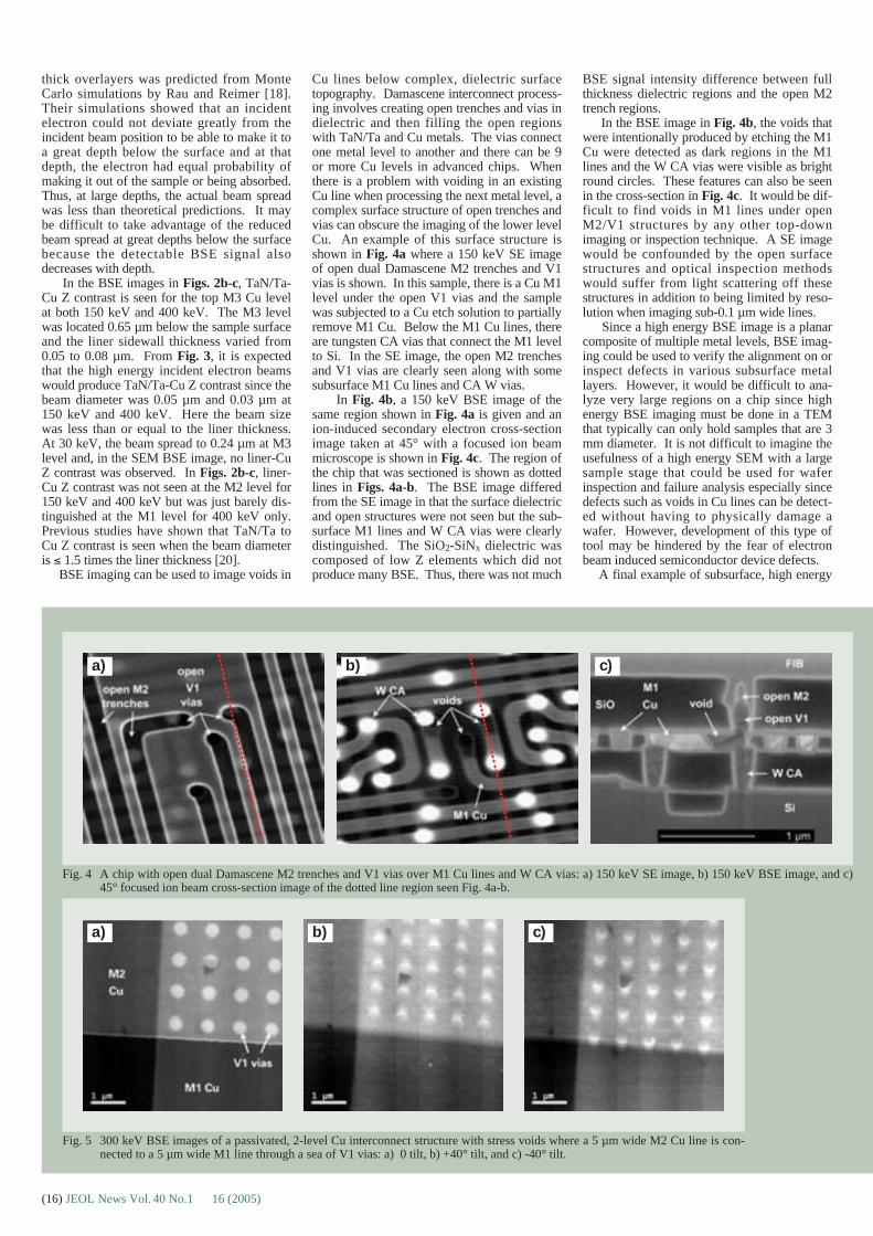
Fig. 2 shows TEM and BSE images of a 3-level Cu electromigration (EM) test structure.Fig 2a is a TEM cross-section image of theanode end of an untested structure showing anupper M3 Cu level under 0.65 µm of SiO2-SiNx, a middle level M2 Cu electromigrationtest structure 1.75 µm below the surface, and aM1 Cu fill structure 2.70 µm below the sur-face. A V2 Cu via connects the M3 line to theM2 test structure. In Figs. 2b and 2c, BSEimages of the anode end of a stressed electro-migration test structure are shown at 150 keVand 400 keV. All three Cu levels are seen inboth images, even the lowest level M1 fillstructure. There is a large void in the top levelM3 line near the V2 contact and this void wasimaged with greater contrast at 150 keV thanat 400 keV. In both BSE images, the edges of
Fig. 1 Passivated, 2-level Cu interconnect structure with stress voids: a) TEM cross-sectionmicrograph, and 400 keV BSE images taken with b) a standard ”L” STEM probe and c)a free lens generated high current BSE probe.
a)
b)
c)
(14) JEOL News Vol. 40 No.1 14 (2005)

the M3 lines have a band of brighter intensitydue to Z contrast from the fine TaN/Ta linerthat encased the Cu lines. The edges of all thelines are sharper at 400 keV than at 150 keVshowing that the subsurface 400 keV BSEimage had better resolution. During the initialstages of penetration into the sample, the beamspreads due to small angle Rutherford scatter-ing while intensity is lost from that compactpart of the beam from wide angle Rutherfordscattering events. At a given depth, a 400 keVelectron beam will be narrower than a 150 keVbeam and will produce a better resolution, sub-surface BSE image. However, the 400 keVelectron beam will penetrate deeper into thesample than the 150 keV beam and will gener-ate fewer BSEs in the upper layers. Thus, theZ contrast generated by the void in the M3layer was less at 400 keV than 150 keV [4].
The ability to detect Z contrast from theTaN/Ta liner was dependent on the liner thick-ness and the beam spread. The beam diameter
varied depending on the incident electron ener-gy, the overlayer material and the depth belowthe surface where the structure was located.The beam diameter at various depths belowthe surface after passing through SiO2-SiNx
dielectric was measured from BSE imagestaken at 30 keV, 150 keV and 400 keV by tak-ing an intensity line scan across the edge ofwide Cu lines where the intensity changedfrom a low signal in the SiO2-SiNx dielectric toa high signal in the Cu line. The 30 keV datawas obtained from BSE images taken on acold field emission SEM. The derivative ofthe line scan was plotted and the beam diame-ter was estimated from the full-width halfmaximum (FWHM) of the derivative peak.When there was TaN/Ta-Cu Z contrast, thebeam diameter was calculated as twice thehalf-width at full maximum where the half-width was taken from the side of the derivativepeak going from dielectric to TaN/Ta.
In Fig. 3, the measured values of the beam
diameters (solid symbols) are plotted versusthe dielectric overlayer thickness. A leastsquares fit to the measured data is shown asdashed lines. For comparison, a theoreticalestimate of the beam spread is given as solidlines. The theoretical values were obtained byusing Goldstein et al.’s [26] beam broadeningrelation for a single Rutherford scatteringevent through SiO2. The theoretical and exper-imentally determined subsurface beam diame-ters agreed for overlayer thicknesses less than0.65 µm. As the SiO2 overlayer thicknessincreased, the measured diameters were lessthan the theoretical values and, for 150 keV,the beam spread began to levels off at SiO2
overlayer thicknesses greater than 2 µm. Eventhough the Goldstein et al. relation wasderived from a single electron scattering eventand these BSE images resulted from multiplescattering events, the experimentally deriveddiameters were less than the measured diame-ters. The leveling off of the beam spread with
0.5 1.0 1.5 2.0 2.5 3.0
0.00
0.05
0.10
0.15
0.20
0.25
0.30
30 keV: calc. meas. meas fit
SiO2 Thickness (µm)
Beam
Dia
mete
r (µm
)
150 keV: calc. meas. meas fit 400 keV: calc. meas. meas fit
Fig. 3 A plot of beam spread versus SiO2 overlayer thickness: symbols are meas-ured values, dotted lines are least squares fits to the measured data and solidlines are theoretical predictions of the beam spread.
Fig. 2 Anode end of a passivated, 3-level electromigration test structure: a) TEM cross-section micrograph of an unstressed structure and BSE images ofa stressed structure taken at b) 150 and c) 400 keV, respectively.
JEOL News Vol. 40 No.1 15 (2005) (15)
thick overlayers was predicted from MonteCarlo simulations by Rau and Reimer [18].Their simulations showed that an incidentelectron could not deviate greatly from theincident beam position to be able to make it toa great depth below the surface and at thatdepth, the electron had equal probability ofmaking it out of the sample or being absorbed.Thus, at large depths, the actual beam spreadwas less than theoretical predictions. It maybe difficult to take advantage of the reducedbeam spread at great depths below the surfacebecause the detectable BSE signal alsodecreases with depth.
In the BSE images in Figs. 2b-c, TaN/Ta-Cu Z contrast is seen for the top M3 Cu levelat both 150 keV and 400 keV. The M3 levelwas located 0.65 µm below the sample surfaceand the liner sidewall thickness varied from0.05 to 0.08 µm. From Fig. 3, it is expectedthat the high energy incident electron beamswould produce TaN/Ta-Cu Z contrast since thebeam diameter was 0.05 µm and 0.03 µm at150 keV and 400 keV. Here the beam sizewas less than or equal to the liner thickness.At 30 keV, the beam spread to 0.24 µm at M3level and, in the SEM BSE image, no liner-CuZ contrast was observed. In Figs. 2b-c, liner-Cu Z contrast was not seen at the M2 level for150 keV and 400 keV but was just barely dis-tinguished at the M1 level for 400 keV only.Previous studies have shown that TaN/Ta toCu Z contrast is seen when the beam diameteris 1.5 times the liner thickness [20].
BSE imaging can be used to image voids in
Cu lines below complex, dielectric surfacetopography. Damascene interconnect process-ing involves creating open trenches and vias indielectric and then filling the open regionswith TaN/Ta and Cu metals. The vias connectone metal level to another and there can be 9or more Cu levels in advanced chips. Whenthere is a problem with voiding in an existingCu line when processing the next metal level, acomplex surface structure of open trenches andvias can obscure the imaging of the lower levelCu. An example of this surface structure isshown in Fig. 4a where a 150 keV SE imageof open dual Damascene M2 trenches and V1vias is shown. In this sample, there is a Cu M1level under the open V1 vias and the samplewas subjected to a Cu etch solution to partiallyremove M1 Cu. Below the M1 Cu lines, thereare tungsten CA vias that connect the M1 levelto Si. In the SE image, the open M2 trenchesand V1 vias are clearly seen along with somesubsurface M1 Cu lines and CA W vias.
In Fig. 4b, a 150 keV BSE image of thesame region shown in Fig. 4a is given and anion-induced secondary electron cross-sectionimage taken at 45° with a focused ion beammicroscope is shown in Fig. 4c. The region ofthe chip that was sectioned is shown as dottedlines in Figs. 4a-b. The BSE image differedfrom the SE image in that the surface dielectricand open structures were not seen but the sub-surface M1 lines and W CA vias were clearlydistinguished. The SiO2-SiNx dielectric wascomposed of low Z elements which did notproduce many BSE. Thus, there was not much
BSE signal intensity difference between fullthickness dielectric regions and the open M2trench regions.
In the BSE image in Fig. 4b, the voids thatwere intentionally produced by etching the M1Cu were detected as dark regions in the M1lines and the W CA vias were visible as brightround circles. These features can also be seenin the cross-section in Fig. 4c. It would be dif-ficult to find voids in M1 lines under openM2/V1 structures by any other top-downimaging or inspection technique. A SE imagewould be confounded by the open surfacestructures and optical inspection methodswould suffer from light scattering off thesestructures in addition to being limited by reso-lution when imaging sub-0.1 µm wide lines.
Since a high energy BSE image is a planarcomposite of multiple metal levels, BSE imag-ing could be used to verify the alignment on orinspect defects in various subsurface metallayers. However, it would be difficult to ana-lyze very large regions on a chip since highenergy BSE imaging must be done in a TEMthat typically can only hold samples that are 3mm diameter. It is not difficult to imagine theusefulness of a high energy SEM with a largesample stage that could be used for waferinspection and failure analysis especially sincedefects such as voids in Cu lines can be detect-ed without having to physically damage awafer. However, development of this type oftool may be hindered by the fear of electronbeam induced semiconductor device defects.
A final example of subsurface, high energy
Fig. 5 300 keV BSE images of a passivated, 2-level Cu interconnect structure with stress voids where a 5 µm wide M2 Cu line is con-nected to a 5 µm wide M1 line through a sea of V1 vias: a) 0 tilt, b) +40° tilt, and c) -40° tilt.
a)
a)
b)
b)
c)
c)
Fig. 4 A chip with open dual Damascene M2 trenches and V1 vias over M1 Cu lines and W CA vias: a) 150 keV SE image, b) 150 keV BSE image, and c)45° focused ion beam cross-section image of the dotted line region seen Fig. 4a-b.
(16) JEOL News Vol. 40 No.1 16 (2005)

BSE imaging is an attempt to do BSE tiltseries tomography on the stress voided, 2-levelCu chip shown in Fig. 1. The region of thechip that was imaged for tilt tomography con-tained a 5 µm wide M2 Cu line connected to a5 µm wide M1 Cu line through a sea of V1vias. This stress voided chip was a good initialcandidate for tomography to be able to visual-ize the depth and location of the voids nearvias. A BSE image of this region of the chipthat was taken in the JEM-3000F field emis-sion TEM at 300 keV is shown at 0° tilt in Fig.5a. The intention of this experiment was totake a series of images at a range of tilts from±70° and then use tomography software toconstruct three-dimensional representations.However, as the tilt increased, the beam trav-eled through increased sample thicknesseswhich caused the beam to broaden. In addi-tion, the signal significantly decreased with tiltand images could only be recorded at maxi-mum tilt values near ±40°, see Figs. 5b-c. Athigh tilts, BSE were forward scattered awayfrom the fixed detector which was situatedbelow the polepiece, 90° from the flat samplesurface. BSE tilt series tomography initiallyseemed to be a good idea since minimal sam-ple preparation was required and a large imag-ing volume could be sampled but the problemsof beam spread and signal loss defeated thisinitial attempt. Improved BSE tilt tomographycould probably be accomplished with a move-able or variable position BSE detector but typi-cally there is limited space in a TEM pole-piece.
Conclusions
BSE imaging of passivated Cu interconnectstructures was used to image voids in Cu lineseven when the lines were buried 1.6 µm belowthe surface or under complex, dielectric sur-face topography. The subsurface image reso-lution and TaN/Ta-Cu Z contrast were limitedby the spreading of the beam that occurredfrom small-angle elastic scattering of the inci-dent electron beam with atoms in the sample.The beam broadening was measured for vari-ous SiO2 surface layer thicknesses and incidentbeam energies. Tilt series BSE tomographywas attempted but was not successful becausethe beam spread increased and the signal sig-nificantly decreased as the sample was tiltedaway from the fixed detector which was locat-ed below the objective polepiece. Commercialdevelopment of a SEM with both high incidentbeam energy and large sample stage capabili-ties could be beneficial to decreasing cost andincreasing yield in a semiconductor fab sincedefect inspection and failure analysis could beperformed on a full wafer without having toscrap the wafer. However there are severaldeterrents that could hinder tool developmentwhich include beam spread and image resolu-tion on the order of the sub-0.1 µm Cu linedimension, low dielectric constant dielectricsthat shrink when imaged with an electronbeam, increased fill structures at each Cu levelthat improves CMP uniformity but obstructsBSE subsurface imaging and electron beaminduced semiconductor device defects.
Acknowledgements
The authors would like to thank Tom Shawfor initiating research in high energy BSE
imaging at IBM T.J. Watson Research Center,John Bruley for helpful technical discussions,and Eric Liniger for providing EM test struc-tures for this study.
References
[1] D. McMullan, “An improved scanningelectron microscope for opaque speci-mens,” Proc. IEE-London 100, 245-259(1952).
[2] S. Kimoto and H. Hashimoto,“Stereoscopic observation in scanningmicroscopy using multiple detectors,”The Electron Microprobe, Proc. Symp.,Washington D. C., Eds. T. D. McKinleyet al., 480-489 (John Wiley & Sons, NewYork, NY, 1964).
[3] O. C. Wells, “Effects of collector take-off angle and energy filtering on the BSEimage in the SEM,” Scanning, 2, 199-216 (1979).
[4] H. Neidrig, “Electron backscatteringfrom thin films,” J. Appl. Phys., 53, R15-R49 (1982).
[5] O. C. Wells, R. J. Savoy and P. J. Bailey,“Backscattered electron (BSE) imagingin the scanning electron microscope(SEM)-measurement of surface layermass-thickness,” Electron BeamInteractions with Solids, SEM, Inc, AMFO’Hare (Chicago) 287-298 (1982).
[6] D. M. Follstaedt, J. A. Van Den Avyle,A. D. Romig, and J. A. Knapp, “High-energy backscattered electron imaging ofvoids in aluminum metallizations,” Mat.Res. Soc. Proc., 225, 223-230 (1991).
[7] E. Castano, J. Maiz, P. Flinn and M.Madden, “In situ observations of dc andac electromigration in passivated Allines,” Appl. Phys. Lett., 59, 129-131(1991).
[8] P. R. Besser, M. C. Madden and P. A.Flinn, “In situ scanning electronmicroscopy observation of the dynamicbehavior of electromigration voids inpassivated aluminum lines,” J. Appl.Phys., 72, 3792-3797 (1992).
[9] M. C. Madden, E. V. Abratowski, T. N.Marieb, and P. A. Flynn, “High resolu-tion observation of void motion in passi-vated metal lines under electromigrationstress,” Mater. Res. Soc. Proc., 265, 33-38 (1992).
[10] H. Todokoro, D. Eng and F. Mizuno,“Observation and measurement ofmicrostructures using a high-energyscanning electron microscope,” HitachiReview, 44, 107-112 (1995).
[11] S. Yamada, T. Ono and F. Mizuno,“Study on irradiation damage to semi-conductor devices by 200 keV electronscaused by BEASTLI method,” Proc.SPIE, 2439, 374-382 (1995).
[12] F. Mizuno, S. Yamada, and T. Ono,“Effects of 50 to 200-keV electrons byBEASTLI method on semiconductordevices,” IEICE Trans. E79-C, 392-397(1996).
[13] V. V. Aristov, E. I. Rau and E. B.Yakimov, “’Apparatus’ electron beammicrotomography in SEM,” Phys. Stat.Sol. (a), 150, 211-219 (1995).
[14] E. I. Rau and V. N. E. Robinson, “Anannular toroidal backscattered electron
analyzer for use in scanning electronmicroscopy,” Scanning, 18, 556-561(1996).
[15] H. Neidrig and E. I. Rau, Informationdepth and spatial resolution in BSEmicrotomography in SEM,” Nuc. Instr.Meth. Phys. Res. B, 142, 523-534 (1998).
[16] J. R. Lowney, M. T. Postek, S. Jones, S.Mayo and M. Creswell, “Simulation andmeasurement of subsurface features inscanning electron microscope metrolo-gy,” Scanning, 30, 219-220 (1998).
[17] J. C. Doan, S. Lee, S.-H. Lee, N. E.Meier, J. C. Bravman and P. A. Flinn, “Ahigh-voltage scanning electronmicroscopy system for in situ electromi-gration testing,” Rev. Sci. Instr., 71,2848-2854 (2000).
[18] E. I. Rau and L. Reimer, “Fundamentalproblems of imaging subsurface struc-tures in the backscattered electron modein scanning electron microscopy,”Scanning, 23, 235-240 (2001).
[19] L. M. Gignac, M. Kawasaki, and S. H.Boettcher, “Imaging of subsurface Cuinterconnects using high energybackscattered electrons,” Electronic Proc.8th Asia-Pacific Conf., ElectronMicroscopy, 727-728 (2004).
[20] L. M Gignac, M. Kawasaki, S. H.Boettcher and O. C. Wells, “Imaging andanalysis of subsurface Cu interconnectsby detecting backscattered electrons inthe scanning electron microscope,” J.Appl. Phys., in press, tentative volume 97(2005).
[21] M. Matsui, S. Machida, H. Todokoro, T.Otaka, and A. Sugimoto, “Observation ofsubsurface structures using high-energySEM,” Metrology, Inspection andProcess Control for MicrolithographyXIX, R. M. Silver, Ed., Proc. SPIE vol.,5752 in press, tentative page 798-805(2005).
[22] D. Edelstein, J. Heidenreich, R.Goldblatt, W. Cote, C. Uzoh, N. Lustig,P. Roper, T. McDevitt, W. Motsiff, A.Simon, J. Dukovic, R. Wachnik, H.Rathore, R. Schulz, L. Su, S. Luce, and J.Slattery, “Full copper wiring in a sub-0.25 µ m CMOS ULSI technology,”IEDM Tech Digest, 773-776 (1997).
[23] D. Edelstein, C. Uzoh, C. Cabral, P.DeHaven, P. Buchwalter, A. Simon, E.Cooney, S. Malhotra, D. Klaus, H.Rathore, B. Agarwala and D. Nguyen,“A high performance liner for copperdamascene interconnects,” Proc. IEEEInt., Interconnect Tech., Conf., 9-11(2001).
[24] H. Neidrig, “Backscattered electrons as atool for film thickness determination,”scanning electron microscopy 1978/I,SEM Inc., Chicago, 841-858 (1978).
[25] O. S. Rajora and A. E. Curzon, “The useof electron image contrast to measure thethickness and composition of thin filmsof light binary alloys,” Thin Solid Films,123, 235-238 (1985).
[26] J. I. Goldstein, J. L. Costley, G.W.Lorimer and S. J. B. Reed, “Quantitativex-ray analysis in the electron micro-scope,” Proc. 10th An. SEM Symp. (O.Johari ed.) SEM Inc., Chicago, IL 1, 315-324 (1977).
JEOL News Vol. 40 No.1 17 (2005) (17)

Recent Development of TEM for AdvancedCeramics
Introduction
Transmission electron microscopy (TEM) isa powerful technique to characterize themicrostructures, and has been intensivelyapplied for advanced ceramics [1]. High reso-lution electron microscopy (HREM), energydispersive X-ray spectroscopy (EDS) and elec-tron energy loss spectroscopy (EELS) are themain techniques to characterize atomic struc-tures, chemical composition and chemicalbonding state in microstructures. These tech-niques have successfully provided manyimportant information to understand the prop-erties in advanced ceramics, i.e., grain bound-ary and interface phenomena are one of thekey factors to understand the nature of theproperties, and hence TEM has been widelyused to elucidate the nature [2]. TEM has thuslong since become an integral part of ceramicresearch. However, the capability of TEManalysis is not always perfect. We frequentlyneed the microstructural information, whichcannot be obtained by a conventional TEM, tofurther understand the properties andmicrostructures in advanced ceramics. In thisarticle, some of recent improvements in TEManalyses are demonstrated.
One of the most striking development forTEM characterization is that theoretical calcu-lations get popular and can be applied to quan-titatively analyze the atomic and electronicstructures. Combining with the theoretical cal-culations, complex and distorted atomic struc-ture are possible to be determined by HREM
[3,4], and the origin of chemical shifts thatappeared in EELS can be quantitatively inter-preted [5,6]. Quantitative analyses for grainboundary structures and energy loss near edgestructures (ELNES) are shown as the exam-ples. In-situ observation in a TEM has con-tributed to the development of materials sci-ence and also played an important role for thebasic knowledge of material phenomena.However, most of results obtained by the in-situ observation are of metals. This is becausethe specimen treatment was difficult for brittleceramics. Although ceramics are expected asthe structural materials, the atomic structure ofthe cleavage plane has even not been clarified.In-situ HREM observation can reveal theatomic structure on the cleavage plane, and anexample of Si3N4 observation will be demon-strated in this paper [7,8]. The resolution ofconventional HREM is 0.17-0.20 nm at 200-300 kV, however, the resolution of about 0.1nm can be achieved by using atomic resolutionhigh voltage electron microscopy (ARHVEM)[9]. It will be shown here that ARHVEM canbe applied to discriminate Ga and N in theGaN thin film. Electron irradiation damage issometimes very serious in characterizing softmaterials by TEM. In this case, low electrondose HREM is possible to reduce the densityof electron dose by using a slow-scan CCDcamera system. An example of direct observa-tion of the channel structures in zeolite wasdemonstrated [10]. Scanning TransmissionElectron Microscopy (STEM) has been recent-ly paid much attention for direct atomic imag-ing and also STEM-EELS-EDS combinedtechnique has emerged to characterize thechemical composition and bonding state atvery narrow region such as grain boundariesand interfaces [11]. Several examples will be
shown in this paper.
Quantitative Analysis
HREM for ceramic grain boundary
HREM has been intensively applied toinvestigate the atomic structures in ceramics,and it has successfully provided importantinformation on microstructural factors such asgrain boundary, interface, lattice defect and soon. The macroscopic properties of ceramicmaterials are strongly influenced by the pres-ence of grain boundaries. Therefore, quantita-tive characterization of the grain boundaries isneeded to obtain materials with better or novelproperties. In order to quantitatively evaluatethe grain boundary atomic structures, well-defined specimens and theoretical calculationsare needed in addition to HREM observations[3]. We have characterized many kinds ofceramic grain boundaries so far [12-15], and aresult for zirconia grain boundary will be intro-duced as an example of quantitative analy-sis[15]. In this study, �= 9 [110] symmetrictilt grain boundary was fabricated by the hot-joining technique as a model specimen.
In order to predict the grain boundary atom-istic structures theoretically, the systematic lat-tice statics calculations were performed usingthe GULP program code [16]. It has been welldemonstrated that the lattice statics calcula-tions were effective method for predicting thestable grain boundary structures in many kindsof ceramic materials [17,18]. In the calcula-tion, the atomistic interactions are described bya potential function which divides the inter-atomic forces into long-range interactions(described by Coulomb’s Law and summatedby the Ewald method) and short-range interac-tions treated by a pairwise function of the
Yuichi Ikuhara
Institute of Engineering Innovation, The University of Tokyo
This paper reviews several recent improvements in new transmission electron microscopy (TEM) to character-ize advanced ceramics. As theoretical calculations are getting popular, quantitative analyses for high resolutionelectron microscopy (HREM) and electron energy loss spectroscopy (EELS) are performed to determine thegrain boundary atomic structures and chemical bonding state in ceramics. TEM in-situ straining technique hasbeen also developed to directly characterize the atomic structures of crack walls in structural ceramics by usingthe crack induced tension (CIT) method which uses the micro-indenter driven by a piezo actuator. Ultra high res-olution electron microscopy (UHREM) is a powerful technique to discriminate the species of atoms which arelocated closer to each other within 0.1 nm, and therefore light elements such as nitrogen and oxygen can bedirectly observed in the structure image. Low electron dose HREM can be applied to characterize soft ceramicssuch as zeolite and biomaterials by using a slow-scan CCD camera system. Scanning transmission electronmicroscopy (STEM) has been recently developed to directly obtain the atomic image by high angle annular darkfield (HAADF) technique and also STEM-EELS-EDS (energy dispersive X-ray spectroscopy) combined techniqueto map the chemical composition and bonding state with a high spatial resolution. Ceramic sciences will be fur-ther developed by the newly developed TEM methods demonstrated here.
2-11-16, Yayoi, Bunkyo-ku, Tokyo 113-8656, Japan.E mail : [email protected]
(18) JEOL News Vol. 40 No.1 18 (2005)

Buckingham. The potential parameters used inthis study were taken from the literaturereported by Lewis and Catlow [19]. The latticeenergies were calculated summing all thepotentials of constituent ions in the calculationcells. The grain boundary excess energies wereestimated by subtracting the calculated latticeenergy for the single crystal cell with the samenumber of ions from the calculated latticeenergy for the cell including the grain bound-ary. The calculated energies were then evaluat-ed as a function of the translation states, andthe atomic configurations with local energyminima were subsequently selected as theequilibrium structures.
Figure 1 shows thus obtained the lowestenergy grain boundary structure predicted bythe lattice statics calculations [15]. The grainboundary excess energy was calculated to be3.01 J/m2, and the lowest energy grain bound-ary structure had a rather large boundaryexpansion of 1.00Å, resulting in the formationof slightly large free volumes at the core of theboundary. The open spaced structures at theboundary core in real material may arise aschanneling contrast on the HRTEM imagewhere there are no atomic columns. Such con-trast would make the interpretation of experi-mental HRTEM image be complicated, andrequire extensive image simulation in variouskinds of possible structure models to deter-mine the real atomistic core structures. Toavoid such ambiguity, the atomic-resolutionhigh-voltage electron microscopy (ARHVEM)was applied to directly determine the atomiccolumn of cation sublattice at the present grainboundary. Cross-sectional HRTEM observa-tions were then mainly carried out by a JEOLJEM-ARM1250 (1250 kV) transmission elec-tron microscope to directly image the atomiccolumn structure of the boundary. In this case,the thickness of the sample specimen was con-trolled to be as thin as about 4nm, and theimage was taken under near the Scherzer defo-cus of about -38nm, so that the atomic
columns can be imaged as black dots reflectingtheir potentials.
Figure 2(a) shows the ARHVEM image ofthe �= 9, {221} grain boundary [15]. As canbe seen in the image, the black dots wereimaged slightly elongated in the [001] direc-tions. This is because the anion sites are locat-ed very close to the cation sites in this direc-tion. Since the open spaced cation sublatticestructure can be directly observed in the micro-graph, this boundary is confirmed to have aperiodical array of asymmetrical structureunits along the grain boundary, as indicated bythe solid lines in Fig. 2 (b). Fig. 2(c) shows thecalculated HRTEM image based on the pre-dicted model as shown in Fig.1. The simulatedimage approximately agrees with the experi-mental image, as for the periodical array ofasymmetrical structure units. The cation siteswith different coordination state are accumu-lated along the calculated �= 9 grain boundarystructure, indicated by the solid arrows in Fig.1. These sites have seven-fold coordination ofoxygen ions, and almost keep the cubic poly-hedra. The density of the coordination defi-cient sites is considered to be related to thegrain boundary energy in zirconia ceramics.
ELNES interpretation
Microscopy approach is very useful forobtaining information about the projectedatomic structure of the specimen, but EELS isalso useful to analyze, not only structures butalso chemical composition and bonding statesfrom the electron illuminated area. Typically,the near edge fine structure of the EEL spec-trum (ELNES) is used for the fine scale char-acterizations. Since ELNES arises from theelectron transition from a core-orbital to theunoccupied bands, the spectral features ofELNES reflect the unoccupied partial densityof states (PDOS) of the objective atom.ELNES therefore contains a wealth of infor-mation on the bonding and electronic structure
around the target atom. In order to quantita-tively interpret ELNES, theoretical calcula-tions using a first principles method are need-ed. To obtain the wave function at the initialstate and the final state, a first-principles bandstructure calculation using the orthogonalizedlinear combinations of atomic orbitals(OLCAO) method was employed. TheOLCAO method is a density functional theory(DFT) based on the local density approxima-tion (LDA) [20]. In the electron transitionprocess, an electronic hole is generated at acore orbital, which is called core-hole. Theattractive potential from the nucleus becomesintense and the wave-function is more local-ized at the nucleus by the presence of the core-hole. The core-hole effect has been shown togreatly affect the accuracy of which the EELspectral features can be reproduced [21,22]. Inthis study, the core-hole effect was fully takeninto account in the self-consistent iterations byremoving an electron at the core orbital andputting it at the lowest band. In order to intro-duce the core-hole, only the core orbital of thecore-holed atom is excluded from the orthogo-nalized process. A sufficiently large supercellis also necessary to minimize the interaction ofneighboring core-holed atoms in the adjacentcells. Figure 3(a) shows the experimentallyobtained O-K ELNES for SiTiO3. Supercellsof 135 atoms were constructed by the 3x3x3 ofthe unit cells for SrTiO3. By employing suchsupercells, approximately 10Å distance can bemade among the core-holed atoms. The fourirreducible k-points were used for the self-con-sistent iteration for the SrTiO3 electronic struc-ture, respectively. Both the final and theground states were separately calculated. Thetheoretical transition energy was evaluated bythe subtraction of the total energy at theground state from that of the final state. Eachtransition probability is broadened using theGaussian function of � =1.0 eV for compari-son with the experimental spectrum. In orderto calculate the high resolution spectrum, eight
Fig. 2 The experimental ARHVEM image of the � = 9, {221} grain boundary. In this condition, the blackdots in the image correspond to the position of the cation column in the crystal. (b) Asymmetric struc-ture units were drawn by the solid lines on the experimental image in (a). (c) The simulated ARHVEMimage using the structure model shown in Fig.1. The image simulation was performed on the condi-tion that the defocus value is -38 nm and a film thickness is 4 nm.
Fig. 1 The lowest energy structure of the � = 9,{221} grain boundary obtained by thelattice statics calculations. Note that highdensity of cation sites with seven-foldcoordination are formed along theboundary, as indicated by the small solidarrows.
JEOL News Vol. 40 No.1 19 (2005) (19)
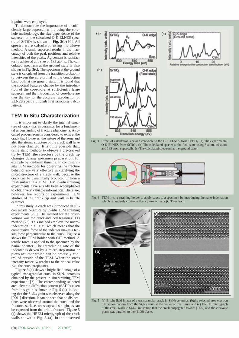
(20) JEOL News Vol. 40 No.1 20 (2005)
k-points were employed.To demonstrate the importance of a suffi-
ciently large supercell while using the core-hole methodology, the size dependence of thesupercell on the calculated O-K ELNES spec-tra of SrTiO3 is shown in Fig. 3(b) [6]. Allspectra were calculated using the abovemethod. A small supercell results in the inac-curacy of both the peak positions and relativeintensities of the peaks. Agreement is satisfac-torily achieved at a size of 135 atoms. The cal-culated spectrum at the ground state is alsoshown in Fig. 3(c). The spectrum at the groundstate is calculated from the transition probabili-ty between the core-orbital to the conductionband both at the ground state. It is found thatthe spectral features change by the introduc-tion of the core-hole. A sufficiently largesupercell and the introduction of core-hole arethus the key for the accurate reproduction ofELNES spectra through first principles calcu-lations.
TEM In-Situ Characterization
It is important to clarify the internal struc-ture of crack tips in ceramics for a fundamen-tal understanding of fracture phenomena. A so-called process zone is considered to exist at thecrack tip. However, the nature of the zone andalso the atomic structure of the crack wall havenot been clarified. It is quite possible that,using static methods to observe a pre-crackedtip by TEM, the structure of the crack tipchanges during specimen preparation, forexample by ion-beam thinning. In contrast, in-situ TEM methods for observing the fracturebehavior are very effective in clarifying themicrostructure of a crack wall, because thecrack can be dynamically produced to form afresh surface in a TEM. TEM in-situ strainingexperiments have already been accomplishedto obtain very valuable information. There are,however, few reports on experimental TEMstudies of the crack tip and wall in brittleceramics.
In this study, a crack was introduced in sili-con nitride ceramics by in-situ TEM strainingexperiments [7,8]. The method for the obser-vations was the crack-induced tension (CIT)method [23]. This method employs the micro-indentation in a TEM, which means that thecompressive force of the indenter makes a ten-sile force perpendicular to the crack. Figure 4shows the TEM holder with CIT method. Atensile force is applied to the specimen by thenano-indenter. The introducing rate of theindenter is driven by a micro-step motor orpiezo actuator which can be precisely con-trolled outside of the TEM. When the stressintensity factor KI reaches to the critical valueKIC, the crack propagates.
Figure 5 (a) shows a bright field image of atypical transgranular crack in Si3N4 ceramicsobtained by the present in-situ straining TEMexperiment [7]. The corresponding selectedarea electron diffraction pattern (SADP) takenfrom this grain is shown in Fig. 5 (b), indicat-ing that the Si3N4 grain was observed along the[0001] direction. It can be seen that no disloca-tions were observed around the crack and thefractured surfaces are sharp and straight, as canbe expected from the brittle fracture. Figure 5(c) shows the HREM micrograph of the crackwalls shown in Fig. 5 (a). In the observed
Fig. 3 Effect of calculation size and core-hole to the O-K ELNES from SrTiO3. (a) The experimentalO-K ELNES from SrTiO3. (b) The calculated spectra at the final state using 8 atom, 40 atom,and 135 atom supercells. (c) The calculated spectrum at the ground state.
Fig. 4 TEM in-situ straining holder to apply stress to a specimen by introducing the nano-indentationwhich is precisely controlled by a piezo actuator (CIT method).
Fig. 5 (a) Bright field image of a transgranular crack in Si3N4 ceramics, (b)the selected area electrondiffraction pattern from the Si3N4 grain at the center of this figure and (c) HREM micrographof the crack walls in Si3N4, indicating that the crack propagated toward [1
-1-20] and the cleavage
plane was parallel to the (11-00) plane.
(a)
(b)
(c)
(a)
(b)
(c)
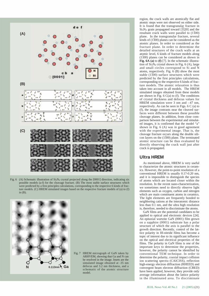
JEOL News Vol. 40 No.1 21 (2005) (21)
region, the crack walls are atomically flat andatomic steps were not observed on either side.It is found that the transgranular fracture inSi3N4 grain propagated toward [1
-1-20] and the
resultant crack walls were parallel to (11-00)
plane. In the transgranular fracture, severalkinds of (11
-00) planes can be considered as the
atomic planes. In order to considered as thefracture plane. In order to determine thedetailed structures of the crack walls at anatomic level, 6 kinds of fracture models along(11
-00) planes can be considered as shown in
Fig. 6A (a) to (f) [7]. In the schematic illustra-tion of Si3N4 crystal shown in Fig. 6 (A), largeand small circles correspond to Si and Natoms, respectively. Fig. 6 (B) show the moststable (11
-00) surface structures which were
predicted by the first principles calculations,corresponding to the respective 6 kinds of frac-ture models. The atomic relaxation is thustaken into account in all models. The HREMsimulated images obtained from these modelsare shown in Fig. 6 C(a) to (f). The conditionsof crystal thickness and defocus values forHREM simulation were 3 nm and –47 nm,respectively. As can be seen in Figs. 6 C (a) to(f), the image contrasts near the cleaved sur-faces were different between these possiblecleavage planes. In addition, from close com-parison between the experimental and simulat-ed images, it is confirmed that the model “a”shown in Fig. 6 (A) was in good agreementwith the experimental image. That is, thecleavage fracture occurs along the double sili-con layers on the (11
-00) plane. The terminated
atomic structure can be thus evaluated bydirectly observing the crack wall just aftercrack is propagated.
Ultra HREM
As mentioned above, HREM is very usefulto characterize the atomic structures in ceram-ics. However, the point-to-point resolution of aconventional HREM is usually 0.17-0.20 nm,and it is impossible to distinguish the speciesof atoms which are located closer within theresolution. In the recent nano-characterization,we sometimes need to directly observe lightelements such as oxygen, carbon and nitrogenwhich are main constituent atoms in ceramics.The light elements are frequently bonded toneighboring cations at the interatomic distanceless than 0.1 nm, and the ultra high resolutionis, therefore, needed to discriminate the atoms.
GaN films are the potential candidates to beapplied to optical and electronic devices [24].An epitaxial wurtzite GaN (0001) film grownon a sapphire (0001) substrate has a polarstructure of which the axis is parallel to thegrowth direction. Recently, control of the lat-tice polarity in III-nitride films has become atopic of interest due to its significant influenceon the optical and electrical properties of thefilms. The polarity in GaN films is one of theimportant keys to determine the properties,however, the polarity cannot be identified byconventional TEM technique. In order todetermine the polarity, coaxial impact collisionion scattering spectra (CAICISS), reflectionhigh-energy electron diffraction (RHEED) andconvergent beam electron diffraction (CBED)have been applied, however, they provide onlyaverage information about the lattice polarityin the illuminated area. To discriminate
Fig. 6 (A) Schematic illustration of Si3N4 crystal projected along the [0001] direction, indicating sixpossible models (a-f) for the cleavage fracture. (B) The most stable surface structures whichwere predicted by a first principles calculations, corresponding to the respective 6 kinds of frac-ture models. (C) HREM simulated images based on the respective fracture models of (a) to (f)in (B).
Fig. 7 HREM micrograph of GaN taken byARHVEM, showing that Ga and N canbe resolved in the image. Insets are thesimulated image obtained at -35 nmdefocus and 3.2 nm thickness, and aschematic of the atomic structuremodel.
(A)
(B)
(C)
N Ga0.113nm

(22) JEOL News Vol. 40 No.1 22 (2005)
between Ga and N, and hence to determine theabsolute polarity, a resolution of 0.113 nm isneeded. We proposed the application ofARHVEM to characterize the GaN film [9,25]. The point-to-point resolution of the elec-tron microscope is about 0.1 nm. ARHVEM,therefore, can be used to directly observe theGa atoms and N atoms on only one image anddetermine the absolute polarity without thecomplicated image analysis required in con-ventional HREM.
Fig.7 shows HREM image of GaN sampleobserved by ARHVEM (JEOL JEM-ARM1250) at an accelerating voltage of 1250kV. Spherical and chromatic aberration con-stants of the objective lens are designed to beCs=1.4 mm and Cc=2.4 mm, respectively. TheHREM image was observed along the <112
-0>
zone axis. The smallest intercolumn distancebetween Ga and N in this orientation is 0.113nm. Initially, the condition of GaN imagingwas systematically checked, because there hasbeen no report on the direct imaging of Ga andN atoms in GaN. In Fig. 7, the inset at theupper right in the micrograph is a simulatedimage obtained using an electron microscopysoftware. The simulated image with Scherzerdefocus and 3.2 nm thickness suggests that Gaand N atomic columns can be imaged as dark-er and lighter spots, respectively. The experi-mental image in Fig. 7 was taken under thesimilar defocus and thickness conditions as thecalculation. In the experiment, a focus seriesaround the Scherzer condition was taken, andthe thickness of the sample was systematicallychecked by comparing the experimental andcalculated images depending on the amount ofdefocus. The experimental image is in goodagreement with the calculated image and itwas found to be possible to discriminatebetween Ga and N atoms by ARHVEM.
Low Electron Dose HREM
Recently, some soft ceramics such as zeo-lites, bioceramics and so on have been paidmuch attention because of their special func-tional properties for environmental assessment.The properties of such soft materials are alsorelated to their atomic structures, and HREMis one of the most effective methods to charac-terize such materials. However, it has beenhard to characterize the soft materials byHREM, because the soft materials are usuallyvery sensitive to electron beam irradiation.They have metastable structures and weakchemical bonding and quite easily damaged byelectron irradiation to form an amorphousstructure. Then, it is usually impossible torecord an image under ordinary conditions ofHREM observations (beam current densi-ty>10A/cm2). Several researches have beenperformed on zeolites using ordinary HREMwith a special technique [26]. However, thistechnique involves taking a picture with filmvery quickly before irradiation damage occursand cannot be used for normal observation. A recording technique for TEM images with aslow-scan charge-coupled–device (CCD) cam-era (SSC camera) has been developed so far,which makes it possible to observe usingHREM with a low electron beam dose [27].An example of observation of the channelstructures in zeolite Y is introduced here.HREM observations were performed on a con-
Fig. 8 HREM micrograph of the channel structure in zeolite Y with the incident beam parallel to the[110] zone axis, showing the presence of 12-member rings as large bright spots.
Fig. 10 (a) STEM image and (b) Lu-K� image obtained by STEM-EDS mapping with the probe sizeof 0.5 nm using a small Cs pole-piece for the grain boundary in the Lu2O3 doped Al2O3.
Fig. 9 HAADF-STEM (Z-con-trast) image for SrTiO3 pro-jected along [001] direc-tion, in which bright andgray contrasts correspondto Sr and Ti, respectively(taken by JEOL JEM-2200FS with Cs corrector).
0.5nm
(100)
2.47 nm
(110)
1.75 nm

JEOL News Vol. 40 No.1 23 (2001) (23)
ventional HREM operating at 200 kV. A SSCcamera was attached to the microscope, andthe images were recorded to the computer inreal time. The SSC camera has a sensitivitymore than several ten times greater than that ofordinary film and is designed in such a waythat the readout noise is less than 1 count rms(at 350k pixel/s sampling rate) by cooling theCCD to –30° to –40°C. Furthermore, itsdynamic range is as wide as 4000, and the lin-earity for the recording is quite accurate withan error less than 1% of full range. The elec-tron dose used for the present HREM studieswas less than about 0.2A/cm2, which corre-sponds to 1/50 of that for the ordinary HREMobservations. Fig.8 shows a HREM micro-graph for zeolite Y(FAU) taken along the[110] direction [10]. Several sizes of whitedots are seen in the figure. The zeolite Y haszinc-blend structure consisting of �-cages, andis stacked as ….ABCABC….in the [111]direction. The �-cages are bonded with 6-member rings to form 12-member rings with adiameter of 0.74nm in the [111] direction.Since these 12-member rings lie along the[110] direction to make a large channel, obser-vation of the channel in zeolite Y was per-formed with the incident beam parallel to the[110] direction. The biggest white dots corre-spond to the channels of 12-member rings.Thus, it is found that the small dots around thebiggest white dots correspond to 4- and 6-member rings in the �-cage.
Scanning TransmissionElectron Microscopy
STEM has been developed to obtain finelyfocused electron probe less than 0.2 nm, andhas applied for characterizing materials.Particularly, a high-angle dark-field STEM(HAADF-STEM) has been used as a kind ofatomic-resolution imaging [28-32]. The con-trast obtained by HAADF-STEM reflects theatomic number (Z), and hence the contrast iscalled Z-contrast. In addition, recent develop-ment of Cs correction technique enables us toobtain further fine probe size less than 0.1 nm,and has been paid much attention for materialsscientists [31,32]. Figure 9 shows an exampleof Z-contrast obtained by STEM with Cs-cor-rector for SrTiO3 projected along [001] direc-tion, in which bright and gray contrasts corre-spond to Sr and Ti, respectively. Z-contrast isthus expected to be very powerful techniquerather than HREM for characterizing ceramics,however, one of the weak points is in observ-ing light elements such as oxygen, nitrogenand carbon because the scattering factor ofthese elements are small. So far, ARHVEMhas been superior to Z-contrast on this point,but very recently, the group of Pennycookexperimentally showed that light elements alsocan be directly imaged by BF-STEM imageusing a Cs corrector [11].
In order to obtain a nano probe smaller than1 nm in a transmission electron microscope,the field emission gun is needed because thesize of illumination is small and the brightnessis high. Grain boundary composition andchemical bonding state for several ceramicshave been successfully investigated by thenano-probe using the small Cs pole-piece.Fig.10 shows (a)STEM image and (b) Lu-K�image obtained by STEM-EDS mapping with
the probe size of 0.5 nm for the grain boundaryin the Lu2O3 doped Al2O3 [33]. It can be clear-ly seen that the continuous segregation layer isformed along the grain boundary. The thick-ness of the segregation layer is about 1 nm.This kind of EDS mapping is also an advan-tage of STEM technique.
Summary
TEM is a very powerful technique to charac-terize microstructures in advanced ceramics.However, we frequently encounter difficultieswhich cannot be solved by conventional tech-niques. The difficulties are in quantitativeanalysis, resolution of in-situ HREM, limita-tion of atomic resolution, spatial resolution andso on. In this case, we need to overcome thedifficulties by developing and contriving themethod to procure essential information onmicrostructures at the necessary conditions. Inthis article, some attempts were demonstratedto show quantitative analysis for grain bound-ary atomic structures and ELNES, in-situstraining TEM, ultra HREM, low dose HREM,high spatial analytical STEM. Now, TEM hasthus many functions, and will add anotherfunctions in the near future. Taking account ofrecent improvements, TEM is not only amicroscope, but also plays a role as a nano-laboratory to process nano-materials and tocharacterize microstructures in dynamic envi-ronments. That is, the fields of TEM is gradu-ally transferring from “Seeing is believing” to“Seeing is creating”. This approach will createa new field of TEM characterization, and con-tribute to the development for the nano-tech-nology in the near future.
Acknowledgements
The author would like to acknowledge thecollaboration of N.Shibata, C. Iwamoto,T.Mizoguchi, S.Ii, J.Buban, H.Yoshida,K.Matsunaga, T.Yamamoto (U.Tokyo),Y.Sasaki, T.Suzuki, T.Hirayama (JFCC) andH. Sawada (JEOL). A part of this work wassupported by the Special Coordination Fundsof the Ministry of Education, Culture, Sports,Science and Technology of the JapaneseGovernment, and also Japan Society for thePromotion of Science, Grant-in-Aid forScientific Research.
References
[1] e. g.: Proc. 14th conf. Electron Microsc.(ICEM), Cancun, Mexico, IOP Pub. Ltd,Danvers USA (1998)
[2] Y. Ikuhara, J. Ceram. Soc. Jpn., 109,S110-S120 (2001)
[3] K. Matsunaga, H. Nishimura, T. Saito, T.Yamamoto and Y. Ikuhara, Philos. Mag.,83, 4071-4082 (2003)
[4] F. Oba, H. Ohta, Y. Sato, H. Hosono, T.Yamamoto and Y. Ikuhara, Phys. Rev. B,70, 125415 (2004)
[5] T. Mizoguchi, M. Sakurai, A. Nakamura,K. Matsunaga, I. Tanaka, T. Yamamotoand Y. Ikuhara, Phys. Rev. B 70, 153101-1-4 (2004).
[6] T. Mizoguchi, J. P. Buban, K. Matsunaga,T. Yamamoto and Y. Ikuhara, Ultra-microscopy, In press (2005)
[7] S. Ii, C. Iwamoto, K. Matsunaga, T.Yamamoto, M. Yoshiya and Y. Ikuhara,Phil. Mag., 84, 2767-2775 (2004)
[8] S. Ii, C. Iwamoto, K. Matsunaga, T.Yamamoto and Y. Ikuhara, J. Electo.Micros., 53 (2), 121-127 (2004)
[9] C. Iwamoto, X. Q. Shen, H. Okumura, H.Matsuhata and Y.Ikuhara, Appl. Phys.Lett., 79, 3941-3943 (2001)
[10] Y. Sasaki, T. Suzuki, Y. Ikuhara and A.Saji, J. Am. Ceram. Soc., 78, 1411-13(1995)
[11] Proc. Microscopy & Microanalysis 2004,Ed. M. Anderson, R. Price, E. Hall, E.Clark and S.Mckernan, Savannah,Georgia, Cambridge Univ. Press (2004)
[12] Y. Ikuhara, N. Shibata, T. Watanabe, F.Oba, T. Yamamoto and T. Sakuma, Ann.Chim. Sci. Mater., 27, S21-30 (2002)
[13] H. Nishimura, K. Matsunaga, T. Saito, T.Yamamoto and Y. Ikuhara J. Am. Ceram.Soc., Vol.86, No. 4, 574-580 (2003)
[14] Y. Sato, T. Mizoguchi, F. Oba, M.Yodogawa, T. Yamamoto and Y. Ikuhara,Appl. Phys. Lett., 84 (26): 5311-5313(2004)
[15] N. Shibata, F. Oba, T.Yamamoto and Y.Ikuhara, Phil. Mag., 84 (23): 2381-2415(2004)
[16] J. D. Gale, J. Chem. Soc. Faraday Trans.,93, 629 (1997).
[17] D. Wolf, 1984, J. Am. Ceram. Soc., 67, 1(1984)
[18] S. Fabrisand C. Elsâsser, Phys. Rev. B.,64, 245117 (2001)
[19] G. V. Lewis and C. R. A. Catlow, J. Phys.C: Solid State Phys., 18, 1149 (1985).
[20] W. Y. Ching, J. Am. Ceram. Soc. 73,3135 (1990).
[21] I. Tanaka, H. Araki, M. Yoshiya, T.Mizoguchi, F. Oba, and H. Adachi, Phys.Rev. B 60 (1999) 4944.
[22] T. Mizoguchi, I. Tanaka, M. Yoshiya, F.Oba, K. Ogasawara, and H. Adachi, Phys.Rev. B 61 (2000) 2180.
[23] Y. Ikuhara, T. Suzuki and Y. Kubo, Philo.Mag. Let., 66, 323-327 (1992)
[24] S. Nakamura, M. Senoh, S. Nagahama, N.Iwasa, T. Yamada, T. Matsushita, Y.Sugimoto and H. Kiyoku, Appl. Phys.Lett., 70, 2753-2756 (1997)
[25] C. Iwamoto, X. Q. Chen, H. Okumura, H.Matsuhata and Y. Ikuhara, J. Appl. Phys.,Vol. 93, No.6, 3264-3269 (2003)
[26] O. Terasaki, Acta Chem. Scand., 45, 785-90 (1991)
[27] P. E. Mooney, G. Y. Fan, C. E. Meyer, K.V. Truong, D. B. Bui and O. L. Krivanek.,p.164, Vol.1, in Proc. 12th ICEM (Seattle,WA, 1990)
[28] S. J. Pennycook and D. E. Jesson, Phys.Rev. Lett., 64, 938 (1990)
[29] N. D. Browning, M. F. Chisholm and S. J.Pennycook, Nature, 366, 143-146 (1993)
[30] Y. Yan, M. F. Chisholm, G. Duscher, A.Maiti, S. J. Pennycook, and S. T.Pantelides : Phys. Rev., 81, 3675-3678(1998)
[31] E. Abe, S. J. Pennycook and A. P. Tsai,Nature, 421, 347 (2003)
[32] N. Shibata, S. J. Pennycook, G. S. Painterand P. F. Becher, Nature, 428 730-733(2004)
[33] H. Yoshida, Y. Ikuhara, and T. Sakuma,,Phil. Mag. Lett., 79, 249-256 (1999)

Advanced Analysis TechnologySupporting SiP
Ken Sugiura
Fukuryo Semiconductor Engineering, Inc.Analysis and Evaluation Center
Introduction
SiP (System in a Package) is an indispensa-ble packaging technology for achieving smallsizing and high-functionality of mobile equip-ments. Packaging density of devices used formobile equipment is ever increasing. Forexample, it is prospected that the minimumpitch of W/B (Wire Bonding) will be reducedto 20 µm from current 40 µm by 2008 and thatthe electrode pattern pitch of full grid typeCSP (Chip Size Package) will also be reducedto 100 µm from current 150 µm by 2008 [1].As the pattern pitch is narrowed, the sizes ofbonding pad and the land on which a metalbump is placed are also reduced, thus, suchfailure modes as peeling of W/B, disconnec-tion of metal bumps, imperfect plating andabnormal precipitation from plating havebecome a serious problem than ever before.
In this paper, we will introduce some exam-ples of failure analysis relating to the defects inelectrical connecting and plating that frequent-ly occur in high density packaged electricaldevices and also describe applications of vari-ous analysis equipments for such analyticaluse.
Features of and ComparisonBetween the CrossSectional ObservationMethods
The cross sectional observation is a base foranalyzing the failure modes in packageddevices. Various methods such as mechanicalpolishing, Microtome, FIB (Focused IonBeam) and ion beam processing are utilizeddepending on respective purposes. Mechanicalpolishing method is widely utilized because itis possible to observe wide areas and theequipment is not expensive in spite that itrequires high-level polishing technique likeworkman. Especially, when observing the
boundary state of intermetallic compound(IMC) and analyzing the composition of mate-rial, the mechanical polishing is the most con-venient method and it is not technologicallyimpossible to observe the cross-section ofultra-micro bump with a thickness less than 20µm. Figure 1 shows an image of a cross-sec-tion of IMC formed at the boundary between asolder bump and an interposer. Regardless ofthe kind of Ni-plating, that is, regardlesswhether it is formed by electroless Ni-P plat-ing or by electrolytic Ni plating, IMC with acomposition of Ni3Sn4 at the boundarybetween eutectic solder is formed, but theirforms are totally different. In case of electro-less Ni-P plating, the IMC takes a pole-like orneedle-like form, while in case of electrolyticNi plating, it takes a layer-like form. In addi-tion, it is known that in case of electroless Ni-Pplating, a P-enriched layer is formed at the sur-face of Ni-P plating because only Ni elementis consumed for diffusive reaction with Sn ele-ment. This status can also be clearly observedby the mechanical polishing method.
Since information obtained by mechanicalpolishing method depends greatly on the pol-ished aspect state, it is impossible to observeand discuss the crystal structure or cracks onthe polished aspect on which mechanical dam-ages such as dents remain.
FIB has also been established as one of thecross-sectional observation methods for ana-lyzing the packaged devices because it givesrelatively small damages to samples and it iseasy to handle. Especially when discussing themetallic crystal structure, channeling imagesobtained from FIB method gives us very effec-tive information. But, since the area processedby this method is limited to 100 µm in widthand 20 µm in depth, it is not appropriate toapply this FIB method to obtain informationfrom wide area of sample. Figure 2 shows thechanneling images obtained from various plat-ing conditions. A method for developing thesample with a cross-section using an ion beamprocessing has been developed recently [2].Since processing area of CP (Cross-sectionPolishing) is relatively wide, about 300 µm in
width and 200 µ m in depth, CP methodenables the wider area to be processed flatterand smoother than FIB method, especiallyeffective for pre-processing the sample toobtain a reflected electron image or EBSP(Electron Backscatter Diffraction Pattern).
Figures 3 and 4 show the reflected electronimage and EBSP image of Au-ball, respective-ly. It can be observed that the crystal located atthe center of the ball became enlarged by ther-mal stress of bonding process and that finecrystals were formed just under the capillarywhere a mechanical stress was applied. Whenprocessing a sample that simultaneouslyincludes both the soft and hard materials andsuch metals as Sn and Ag of which etchingrate is high with CP method, it should benoticed that beam damage may remain, mak-ing observation difficult.
Identifying the Au-Al Compound
W/B using a high-purity Au wire is amethod for electrically connecting the semi-conductor chip to the substrate that holds thechip, and the state of Au-Al compound formedat the boundary between Au-ball and Al-pad isan important measure of reliability of devices.
Historically, EPMA (Electron Probe MicroAnalysis) method has been utilized for identi-fying the Au-Al compound. However, sincethe thickness of compound layer just afterbonding process is very thin, it has been verydifficult to identify the compound in principleof EPMA measurement. FEAES (FieldEmission type Auger Electron Spectroscopy)is good at analyzing a very small area with adiameter less than 1 µm. Accuracy of quantita-tive determination of AES method is inferiorto EPMA method, and it is said that AESmethod is not adequate to identify the IMC.But, high reliability can be obtained by execut-ing comparative analysis against the standardmaterials. Figure 5 shows a qualitative spec-trum of Au-Al standard compound and Table1 shows the results of semi quantitative deter-mination that has corrected the relative sensi-
1-1-1 Imajukuhigashi Nishi-ku Fukuoka 819-0192 JapanEmail: [email protected]
(24) JEOL News Vol. 40 No.1 24 (2005)

tivity for Au and Al. Since, although the relative atomic ratio of
Au and Al does not completely coincide withthe ideal composition calculated, errors fall inthe range of ±few percents, we judged that it ispossible to identify the Au-Al compound usingthis AES method. Figures 6 and 7 show thecomposition of the compound formed aftermold curing and after storage at 200°C for 168hours, respectively.
The dominated layer after mold curing isAu5Al2, and there exists Au4Al in Au side,Au2Al and AuAl in Al side. The dominatedlayer after storage at 200°C for 168 hourschanged to Au4Al and there exists Au2Al andAu5Al2 remained around the ball. Change ofthe dominated layer is considered to resultbecause a growing speed of compound byheating is limited to the diffusion speed of Au,and consequently, the Au4Al as the most Au-rich layer was stabilized. On the other hand,defects are observed in the boundary betweenAu wire and Au4Al layer, and since thereexists strong Oxygen, it is considered thatthese defects are traces of compound’s erosioncaused by moisture included in mold resin.TEM (Transmission Electron Microscope)observation image of the defect is shown inFig. 8. Defects are composed of three types ofmodes, Phase-A, Phase-B and Phase-C. ASshown by EDS profile in Figs. 9 and 10, itbecame clear that the dominant layer of Phase-B has a composition consisting of only Al andOxygen without Au, and Phase-C that distrib-utedly exists in Phase-B includes Au.Although it has been considered that the ero-sion of Au-Al compound is generally causedby Al-bromide as the result of a reactionbetween Br included in mold resin as a fireretarding material and Au4Al [3].
But, in both of the above described FEAESand EDS methods, the energy positions of Brand Al overlap in the same location, it isimpossible to detect the existence of Br.Therefore, we have confirmed the existence ofBr in defects by EPMA analysis. Figure 11shows a EPMA profile. Br was not detected inFig. 11. Thus, it was suggested that there is a
Fig. 3 Reflected electron image of Auball (CP FE SEM).
Fig. 4 BESP image of Au ball.
Fig. 1 State of forming of IMC (mechanical polishing FE SEM).
Fig. 2 Channeling images of electrode plating (FIB).
micro-crystals
JEOL News Vol. 40 No.1 25 (2005) (25)

possibility that erosion is not only acceleratedby halogen element, but also promoted by justmoisture as well.
Analysis on peeling-off of
electroless Au/Ni-P plating
Electroless Au/Ni-P plating is utilized forsurface finishing of printed wiring boardsincluding interposers.
Since the flash Au plating is formed by asubstitution reaction with Ni, when an excesssubstitution reaction occurs, underlying Ni-Pplating layer is pitted by corrosion causingpeeling-off ultra-sonic bonding and degrada-
tion of the adhesion strength of solder [4].Figures 12 to 5 show the AES depth profile
and the surface state of Ni-P layer after remov-ing the flash Au, in cases of normal platingand abnormal plating, respectively. In case ofabnormal Au/Ni-P plating, P-enriched layerwas observed at the boundary between Au andNi-P, and it was also known that carbon andoxygen exist in Ni-P plating layer. On theother hand, pitting corrosion was observedalong the grain boundary on Ni-P surface afterremoval of Au.
Figures 16 and 17 show the FIB cross-sec-tional images of the part where Au plating waspeeled off and remained normally, respective-
ly. At the boundary between Au and Ni-P lay-ers, an amorphous layer with 0.2 µm thicknessincluding a micro-void was observed, and itwas confirmed that peeling off occurred at theboundary between Au plating layer and theamorphous layer.
Taking account of the state of pitting corro-sion on the surface of Ni-P plating layer, AESanalysis result and FIB cross-sectional image,we concluded that the amorphous layer is aAu/Ni substitution layer formed by an excessreaction and that the pitting corrosion observedat the surface of Ni-P layer after removal ofAu is a trace that an excess reaction took placesignificantly along the grain boundary. In addi-
Fig. 9 EDS profile of Phase-B.
Fig. 10 EDS profile of Phase-C.
Fig. 11 EPMA profile of defect position.Fig. 8 TEM image of defect part.
Fig. 5 Spectrum of Au-Al standard (FEAES).
Table. 1 Composition of Au-Al IMC.
Fig. 6 (a) Compound composition around the Au ball (after molding). (b) Compound composition at the center area of Au ball (after molding).
Fig. 7 (a) Compound composition around the Au ball (after 200°C �168hrs).(b) Compound composition at the center area of Au ball (after 200°C �168hrs).
(a)
(a)
(b)
(b)
(26) JEOL News Vol. 40 No.1 26 (2005)

tion, the excess reaction resulted from Ni-Player including carbon. Figure 18 shows anestimated structure of the Au exfoliated part.In order to accurately analyze the concentra-tion distribution of carbon (C), sulfur (S) andoxide (O) of which abnormal eutectoid intoNi-P layer is concerned, we used SIMS(Secondary Ionization Mass Spectrometer)analysis. Figures 19 and 20 show SIMS pro-files of the normal and abnormal plating,respectively. The horizontal axis correspondsto concentration gradient in the depth direc-tion. It is known that there is no difference inthe concentration distribution of Au, Ni and Pas the components of plating between normal
and abnormal plating, while the concentrationof C, S and O elements included in abnormalplating are higher than that of normal plating.
Then, in order to clear the origin of theseimpurities, we tried to analyze organic compo-nents included in Ni-P solution that was usedfor processing the abnormal plating taking astandard Ni-P solution as a reference. As forthe organic components with low boilingpoint, we applied GC/MS (Gas Chromatograph/Mass Spectrometer) analysis after solid-phasemicro extraction. While, as for the organiccomponents with high boiling point, weapplied 13C FT-NMR (Fourier Transform-Nuclear Magnetic Resonance) analysis after
letting the residual material after heating anddrying the plating solution dissolved into aheavy chloroform solution. Figures 21 and 22show the results of GC/MS and FT-NMRanalysis on the used solutions.
No volatile components included regardlessof the used solutions after bath-plating, and cit-rate, succinate, EDTA and ureic compound,etc. were detected as non-volatile components.On the other hand, from only the used solu-tion, kinds of polyethylene-glycol-diacrylate,kinds of amino-alkyl-phenon, azobisisobuty-lonitrile and its resolvent were detected.
It is considered that the organic componentdetected from the only used solution was
Fig. 12 Depth profile of normal plating(AES).
Fig. 14 Depth profile of abnormal plating(AES).
Fig. 16 Cross-sectional view of peeled-offpart (FIB).
Fig. 13 Surface of normal plating (afterremoving Au).
Fig. 15 Surface of abnormal plating (afterremoving Au).
Fig. 17 Cross-sectional view of normal part(FIB).
Fig. 19 Impurity concentration distribution of normalplating (SIMS).
Fig. 20 Impurity concentration distribution of abnor-mal plating (SIMS).
Fig. 18 Estimated structure of Au plating peeled-offpart.
JEOL News Vol. 40 No.1 27 (2005) (27)

brought into Ni-P solution and condensedwithin the bath. And it was estimated that thedetected amino-alkyl-phenon, azobisisobuty-lonitrile and its resolvent originated from radi-cal additive included in resin material.Actually we confirmed the status of Au/Ni-Pwith and without additive by FIB method andwe also confirmed that the state of IMCformed at the boundary between solder andNi-P plating after attaching the eutectic solderballs. Figures 23 to 26 show the observedresults. In case of Au/Ni-P plating with addi-tive, an amorphous layer accompanied withvoids at the surface layer of Ni-P plating wasreproduced. And at the boundary between thesolder and Ni-P plating, we could reproducethat no Ni3Sn4 compounds were formed.
As described above, it was estimated thatthe Ni-P plating layer becomes vulnerable andthe bonding power of Ni element was weak-ened because the organic components getmixed in Ni-P solution bath was made eutec-toid. Therefore, Ni-element becomes easily todiffuse under the presence of reacting speciessuch as Au or Sn, and it generates an excesssubstitution reaction in succeeding Au platingprocess or soldering process, but the effect ofkinds of aminophenon and organic compo-nents including sulfur element is significant.The result that SIMS analysis detected highlyconcentrated sulfur from abnormal platinglayer corresponds to this idea.
Conclusions
We have introduced some examples relatingto analysis on plating layer in packageddevices. As packaging technology advances,needs for analysis also becomes higher andmore complicated. Today, analysis engineersare required not only to seek analysis technolo-gy but also to obtain an ability to give exactadvices originated from empirical rules and togive so called “total solution”. Essentialdemand in the analysis market is moving toconsultation from the excellence of operationskill.
References
[1] ITRS2004 Update[2] Masateru Shibata.: Creation of cross-sec-
tional surface specimen using an Argonbeam, Nihon Denshi News, Vol. 35, No.1,pp.24-27(2003)
[3] Tomohiro, et al,: Corrosion behavior andjunction reliability of intermetallic com-pound phase in Au/Al junction, J., ofJapan Inst. Metals, vol. 63, No.3, pp. 406-415 (1999)
[4] Reiko Aiba, et al.: Strength of solder junc-tion with Au plating layer formed by newnon-cyan displacement type electrolessplating without pitting corrosion, Digest of19th Electronic Packaging AcademicConference on Electronic Packaging, pp.187-188 (2005)
Fig. 21 Low boiling point organic component in abnormal plating solution (GC/MS).
Fig. 23 Status of Au/Ni-P forming (FIB).
Fig. 25 Status of Au/Ni-P forming (FIB).
Fig. 24 Status of IMC forming (cross-sectionalFE SEM).
Fig. 26 Status of IMC forming (cross-sectionalFE SEM).
Fig. 22 High boiling point organic component in abnormal plating solution (FT-NMR).
With Additive
With Additive
(28) JEOL News Vol. 40 No.1 28 (2005)

Introduction of Fully Automatic NMR Measurement Tool “GORIN” for Protein Solution
Introduction
This article explains a fully automatic NMRmeasurement tool “GORIN” for protein NMR.This is an optional software for the basic NMRcontrol software “Delta V4.3” of the JNM-ECA/ECX series FT-NMR system. This soft-ware can operate only with the Delta V4.3 orlater. Moreover, the HCN triple resonanceprobe is required in the spectrometer configu-ration. Since this article will describe mainlyspecial functions, please contact the JEOLoffice for more details.
Software Configuration
The following five programs are configuredas the GORIN (Gorgeous Operation Routine)(Fig.1).� MUSASHI:
Parameter optimization tool� OTSU:
Continuous measurement tool� TAQUAN DAICHOU:
Parameter database � IORI:
Automatic measurement execution module� MATA8:
Measurement dimension transfer tool� Others:
Pulse programs, process lists, and templates
MUSASHI
The parameter optimization in “MUSASHI”is mainly used to measure 90°pulse width.Accurate pulse width can be calculated fromarray measurement data using nonlinear leastsquare fitting. In fully automatic measurement,this program is invoked for parameter calibra-tion, and operated in the background (Fig. 2).
OTSU
Continuous observation tool “OTSU” is aneffective tool when measuring linearity ofpower amplifier output. Array measurementsare performed continuously while changingthe parameters such as attenuator, and thissoftware plots the result calculated for eachmeasurement data using MUSASHI in thegraph (Fig. 3).
Fig. 1 Software configuration of GORIN.
(a) MUSASHI.
(b) Intensity data list of each slice detectedfrom array measurement (optimization cal-culation is performed based on this data).
(c) Optimization result by MUSASHI.
FT NMR New Technical Introduction
Fig. 2
JEOL News Vol. 40 No.1 29 (2005) (29)
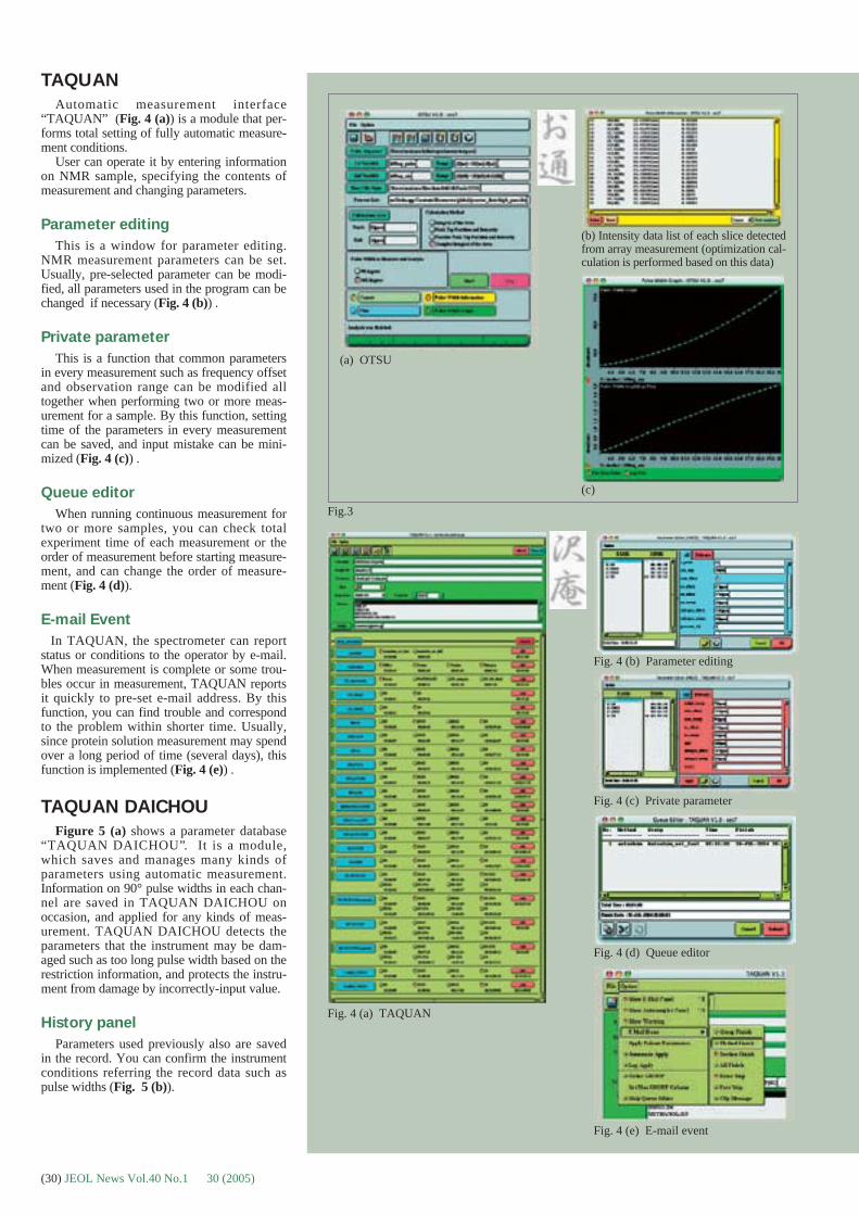
TAQUAN
Automatic measurement interface“TAQUAN” (Fig. 4 (a)) is a module that per-forms total setting of fully automatic measure-ment conditions.
User can operate it by entering informationon NMR sample, specifying the contents ofmeasurement and changing parameters.
Parameter editing
This is a window for parameter editing.NMR measurement parameters can be set.Usually, pre-selected parameter can be modi-fied, all parameters used in the program can bechanged if necessary (Fig. 4 (b)) .
Private parameter
This is a function that common parametersin every measurement such as frequency offsetand observation range can be modified alltogether when performing two or more meas-urement for a sample. By this function, settingtime of the parameters in every measurementcan be saved, and input mistake can be mini-mized (Fig. 4 (c)) .
Queue editor
When running continuous measurement fortwo or more samples, you can check totalexperiment time of each measurement or theorder of measurement before starting measure-ment, and can change the order of measure-ment (Fig. 4 (d)).
E-mail Event
In TAQUAN, the spectrometer can reportstatus or conditions to the operator by e-mail.When measurement is complete or some trou-bles occur in measurement, TAQUAN reportsit quickly to pre-set e-mail address. By thisfunction, you can find trouble and correspondto the problem within shorter time. Usually,since protein solution measurement may spendover a long period of time (several days), thisfunction is implemented (Fig. 4 (e)) .
TAQUAN DAICHOU
Figure 5 (a) shows a parameter database“TAQUAN DAICHOU”. It is a module,which saves and manages many kinds ofparameters using automatic measurement.Information on 90° pulse widths in each chan-nel are saved in TAQUAN DAICHOU onoccasion, and applied for any kinds of meas-urement. TAQUAN DAICHOU detects theparameters that the instrument may be dam-aged such as too long pulse width based on therestriction information, and protects the instru-ment from damage by incorrectly-input value.
History panel
Parameters used previously also are savedin the record. You can confirm the instrumentconditions referring the record data such aspulse widths (Fig. 5 (b)).
Fig. 4 (b) Parameter editing
Fig. 4 (c) Private parameter
Fig. 4 (d) Queue editor
Fig. 4 (e) E-mail event
(b) Intensity data list of each slice detectedfrom array measurement (optimization cal-culation is performed based on this data)
Fig. 4 (a) TAQUAN
(a) OTSU
Fig.3
(c)
(30) JEOL News Vol.40 No.1 30 (2005)
JEOL News Vol. 40 No.1 31 (2005) (31)
IORI
Automatic measurement execution module“IORI” sends measurement conditions direct-ly to the spectrometer. Although measure-ments are performed in the order of QUEUErecorded in IORI, you can also change theorder of measurement here (Fig. 6 ).
MATA8
This measurement dimension transfer toolmutually transfers a pulse program from 1D (1dimension) version to higher dimension up to4D (4 dimensions) version. This is the tool forpulse program development. To transfer meas-urement dimension, description of the flag forMATA8 in the pulse program is necessary. Inthe standard pulse program, although you canselect up to 8 kinds of measurement dimen-sion: 1D, 2DXY, 2DXA, 3DXYZ, 3DXYA,3DXZA and 4D, the kinds of measuringdimension transformed actually differ depend-ing on the pulse program.
Others
Pulse program
This is a pulse program group provided forprotein solution NMR measurement. All thepulse programs are saved in “for_protein” ofglobal. The pulse programs for data acquisitionand pulse programs for calibration are saved inthe experiments and “sword_for_taquan”,respectively. These pulse programs have beencreated assuming that they are used withTAQUAN.
Process list
Corresponding process list has been provid-ed for the data acquisition program. Theprocess lists are saved in “protein_lists” ofglobal.
Template
This is a template file for TAQUAN. Textand binary editions are provided.
Conclusion
If you use the GORIN, an automatic NMRmeasurement tool for protein solution, you canobtain good spectrum similar to the spectrumobtained by professional person simply byone-button operation without complicatedoperation and difficult calibration. Figure 7demonstrates a high-quality 3D NMR dataobtained by the GORIN. We hope that thistool makes NMR measurement easy for pro-tein solution and application field of proteinsolution NMR will be expanded.
Fig. 5(a) TAQUAN DAICHOU.
Fig. 5(b) History panel.
Fig. 6 IORI.
Fig. 7 Three dimensioncubic display forHNCACB spectrummeasured usingGORIN.
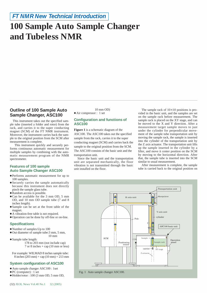
Manipulator
V axis unit
H axia unit
Sample
Sample rack
XY stage
Z actuator
100 Sample Auto Sample Changer and Tubeless NMR
Outline of 100 Sample AutoSample Changer, ASC100
This instrument takes out the specified sam-ple tube (inserted a folder and rotor) from therack, and carries it to the super conductingmagnet (SCM) of the FT NMR instrument.Moreover, the instrument carries back the sam-ple to the original position from the SCM aftermeasurement is complete.
This instrument quickly and securely per-forms continuous automatic measurement formultiple samples by combining with the auto-matic measurement program of the NMRspectrometer.
Features of 100 sample Auto Sample Changer ASC100
� Performs automatic measurement for up to100 samples.
� Securely carries the sample automaticallybecause this instrument does not directlypinch the sample glass tube.
� Random access is possible.� Can be available for the 3 mm OD, 5 mm
OD, and 10 mm OD sample tube (7 and 8inches length).
� Sample can be set at the front table of themagnet.
� A vibration-free table is not required.� Operation can be done by off-line or on-line.
Specifications
� Number of samples:Up to 100� Out diameter of sample tube:3 mm, 5 mm,
10 mm� Sample tube length:
178 to 203 mm (not include cap)7 or 8 inches + cap (10 mm or less)
For example: WILMAD 8 inches sample tube:8 inches (203 mm) + cap (10 mm) = 213 mm
System configuration of ASC100
� Auto sample changer ASC100 : 1set� PC (computer) : 1 set� Holder/rotor : 100 (3 mm OD, 5 mm OD,
10 mm OD)� Air compressor : 1 set
Configuration and functions ofASC100
Figure 1 is a schematic diagram of theASC100. The ASC100 takes out the specifiedsample from the rack, carries it to the superconducting magnet (SCM) and carries back thesample to the original position from the SCM.The ASC100 consists of the basic unit and thetransportation unit.
Since the basic unit and the transportationunit are separated mechanically, the floorvibration is not transmitted through the basicunit installed on the floor.
The sample rack of 10�10 positions is pro-vided in the basic unit, and the samples are seton the sample rack before measurement. Thesample rack is placed on the XY stage, and canbe moved to the X and Y direction. After ameasurement target sample moves to justunder the cylinder for perpendicular move-ment of the sample tube transportation unit bymoving the sample rack, the sample is insertedinto the cylinder of the transportation unit bythe Z axis actuator. The transportation unit liftsup the sample inserted in the cylinder by alifter, and move it center position on the SCMby moving to the horizontal direction. Afterthat, the sample tube is inserted into the SCMsimilar to usual measurement.
After measurement is complete, the sampletube is carried back to the original position on
Fig. 1 Auto sample changer ASC100.
FT NMR New Technical Introduction
(32) JEOL News Vol.40 No.1 32 (2005)
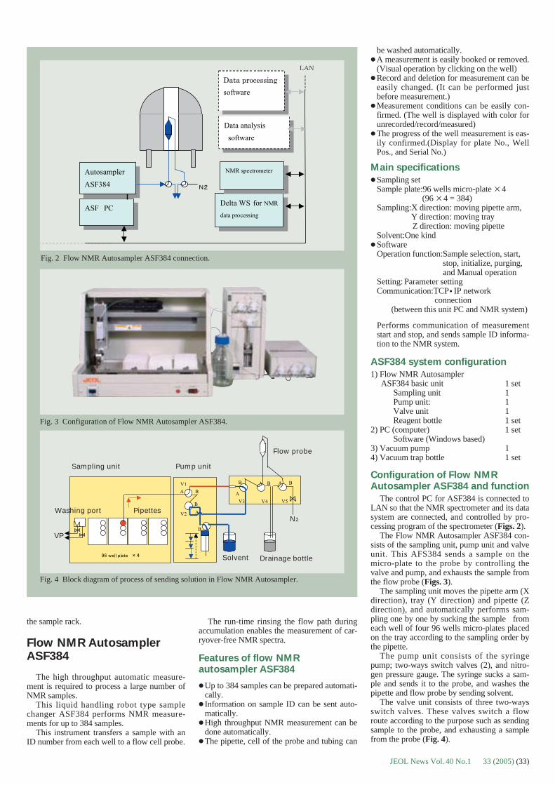
the sample rack.
Flow NMR AutosamplerASF384
The high throughput automatic measure-ment is required to process a large number ofNMR samples.
This liquid handling robot type samplechanger ASF384 performs NMR measure-ments for up to 384 samples.
This instrument transfers a sample with anID number from each well to a flow cell probe.
The run-time rinsing the flow path duringaccumulation enables the measurement of car-ryover-free NMR spectra.
Features of flow NMR autosampler ASF384
� Up to 384 samples can be prepared automati-cally.
� Information on sample ID can be sent auto-matically.
� High throughput NMR measurement can bedone automatically.
� The pipette, cell of the probe and tubing can
be washed automatically.� A measurement is easily booked or removed.
(Visual operation by clicking on the well)� Record and deletion for measurement can be
easily changed. (It can be performed justbefore measurement.)
� Measurement conditions can be easily con-firmed. (The well is displayed with color forunrecorded/record/measured)
� The progress of the well measurement is eas-ily confirmed.(Display for plate No., WellPos., and Serial No.)
Main specifications � Sampling set
Sample plate:96 wells micro-plate �4(96 �4 = 384)
Sampling:X direction: moving pipette arm, Y direction: moving tray Z direction: moving pipette
Solvent:One kind� Software
Operation function:Sample selection, start,stop, initialize, purging,and Manual operation
Setting: Parameter settingCommunication:TCP � IP network
connection(between this unit PC and NMR system)
Performs communication of measurementstart and stop, and sends sample ID informa-tion to the NMR system.
ASF384 system configuration
1) Flow NMR Autosampler ASF384 basic unit 1 set
Sampling unit 1 Pump unit: 1Valve unit 1Reagent bottle 1 set
2) PC (computer) 1 setSoftware (Windows based)
3) Vacuum pump 14) Vacuum trap bottle 1 set
Configuration of Flow NMRAutosampler ASF384 and function
The control PC for ASF384 is connected toLAN so that the NMR spectrometer and its datasystem are connected, and controlled by pro-cessing program of the spectrometer (Figs. 2).
The Flow NMR Autosampler ASF384 con-sists of the sampling unit, pump unit and valveunit. This AFS384 sends a sample on themicro-plate to the probe by controlling thevalve and pump, and exhausts the sample fromthe flow probe (Figs. 3).
The sampling unit moves the pipette arm (Xdirection), tray (Y direction) and pipette (Zdirection), and automatically performs sam-pling one by one by sucking the sample fromeach well of four 96 wells micro-plates placedon the tray according to the sampling order bythe pipette.
The pump unit consists of the syringepump; two-ways switch valves (2), and nitro-gen pressure gauge. The syringe sucks a sam-ple and sends it to the probe, and washes thepipette and flow probe by sending solvent.
The valve unit consists of three two-waysswitch valves. These valves switch a flowroute according to the purpose such as sendingsample to the probe, and exhausting a samplefrom the probe (Fig. 4).
Fig. 2 Flow NMR Autosampler ASF384 connection.
Fig. 3 Configuration of Flow NMR Autosampler ASF384.
Fig. 4 Block diagram of process of sending solution in Flow NMR Autosampler.
Sampling unit Pump unit
VP
Pipettes
Flow probe
N2
Solvent Drainage bottle
Washing port
JEOL News Vol. 40 No.1 33 (2005) (33)

Latest Information and Future for ALICE2 Software
Introduction
Recently, the metabolome analysis ormetabonomics, which covers all metabolites, isgiven attention along with progressing genomeand proteome science. Generally, themetabolome analysis using NMR uses a pro-ton spectrum. However, since a biologicalsample includes many low molecular weightsubstances and biological polymers, the protonspectrum is very complicated by many over-lapping peaks. Moreover, since there are many
small signals in the spectrum, it is difficult todistinguish them from noise. So assigning eachpeak as ordinary analysis method cannot per-form structure analysis. Therefore, patternrecognition approach is applied to the classifi-cation of the spectra for these samples bymeasuring many samples and performing sta-tistical analysis. Metabolic difference andtime-lapse change can be detected by thismethod. So far, however, there was not thesimple software with this metabolome analy-sis.
This time, since we develop ALICE2 formetabolome that full automatic metabolomeanalysis function is added to the ALICE2 ofNMR processing software, we will introduce itin this article.
We will explain the outline of the developedprogram first, and explain results of the inspec-tion experiment of this program using mixturesamples. However, since handling of a biologi-cal sample is difficult, we try to analyze theproton spectra of various kinds of tea as anexample of the analysis of mixture sample.
Fig. 2 Phase corrected spectrum (upper), and Absolute differentialspectrum (lower).
-Application for metabonomics-
Fig. 1 Process of metabolome analysis.
Data input
Spectrum processing(Absolute Differential
Calculus Method )
Data reduction by bucket integration
Output of analysis result (MS-Excel)
Multivariate analysis(PCA,SIMCA)
FT NMR New Technical Introduction
(34) JEOL News Vol.40 No.1 34 (2005)
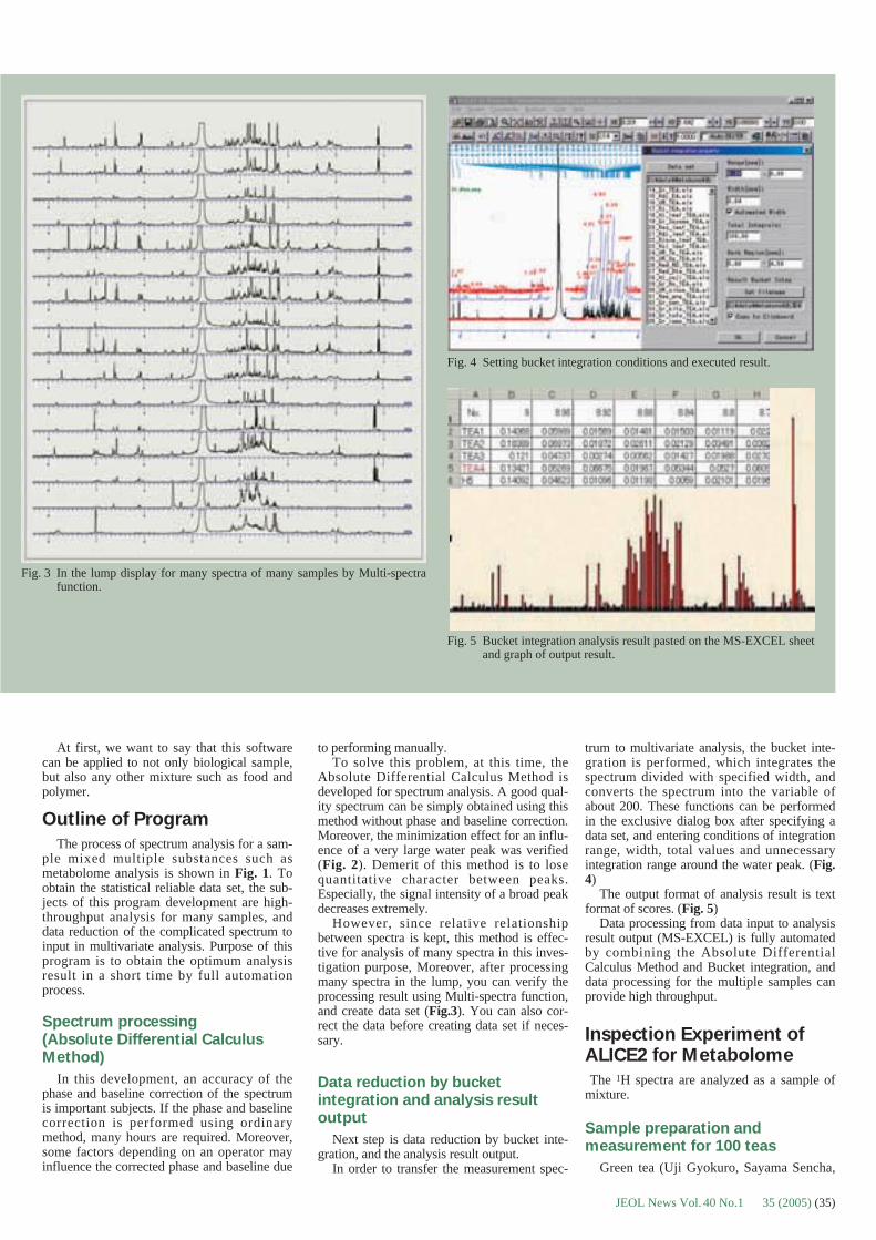
At first, we want to say that this softwarecan be applied to not only biological sample,but also any other mixture such as food andpolymer.
Outline of Program
The process of spectrum analysis for a sam-ple mixed multiple substances such asmetabolome analysis is shown in Fig. 1. Toobtain the statistical reliable data set, the sub-jects of this program development are high-throughput analysis for many samples, anddata reduction of the complicated spectrum toinput in multivariate analysis. Purpose of thisprogram is to obtain the optimum analysisresult in a short time by full automationprocess.
Spectrum processing (Absolute Differential CalculusMethod)
In this development, an accuracy of thephase and baseline correction of the spectrumis important subjects. If the phase and baselinecorrection is performed using ordinarymethod, many hours are required. Moreover,some factors depending on an operator mayinfluence the corrected phase and baseline due
Fig. 3 In the lump display for many spectra of many samples by Multi-spectrafunction.
Fig. 4 Setting bucket integration conditions and executed result.
Fig. 5 Bucket integration analysis result pasted on the MS-EXCEL sheetand graph of output result.
to performing manually. To solve this problem, at this time, the
Absolute Differential Calculus Method isdeveloped for spectrum analysis. A good qual-ity spectrum can be simply obtained using thismethod without phase and baseline correction.Moreover, the minimization effect for an influ-ence of a very large water peak was verified(Fig. 2). Demerit of this method is to losequantitative character between peaks.Especially, the signal intensity of a broad peakdecreases extremely.
However, since relative relationshipbetween spectra is kept, this method is effec-tive for analysis of many spectra in this inves-tigation purpose, Moreover, after processingmany spectra in the lump, you can verify theprocessing result using Multi-spectra function,and create data set (Fig.3). You can also cor-rect the data before creating data set if neces-sary.
Data reduction by bucket integration and analysis resultoutput
Next step is data reduction by bucket inte-gration, and the analysis result output.
In order to transfer the measurement spec-
trum to multivariate analysis, the bucket inte-gration is performed, which integrates thespectrum divided with specified width, andconverts the spectrum into the variable ofabout 200. These functions can be performedin the exclusive dialog box after specifying adata set, and entering conditions of integrationrange, width, total values and unnecessaryintegration range around the water peak. (Fig.4)
The output format of analysis result is textformat of scores. (Fig. 5)
Data processing from data input to analysisresult output (MS-EXCEL) is fully automatedby combining the Absolute DifferentialCalculus Method and Bucket integration, anddata processing for the multiple samples canprovide high throughput.
Inspection Experiment ofALICE2 for Metabolome
The 1H spectra are analyzed as a sample ofmixture.
Sample preparation and measurement for 100 teas
Green tea (Uji Gyokuro, Sayama Sencha,
JEOL News Vol. 40 No.1 35 (2005) (35)

Yamanashi Hojicha, Chinese green tea) blacktea (Darjeering, Assam, Chinese black tea),oolong (Tekkanon, Okinnkei ) are extractedwith hot water for 3 minutes at 75°C, and thetop is used after centrifuging.
Measurement condition: Deuterated water isadded 10 %, and water signal is eliminatedusing the pre-salutation method.
Instrument: JNM-ECA500 (Proton reso-nance frequency is 500 MHz.)
Typical spectra of teas are shown in Fig. 6.In the spectra, typical peaks of catechin, thea-nine, caffeine and many amino acids appear.The peak of amino acid cannot be assignedbecause many amino acids are included.Spectrum pattern of green tea differs fromspectrum of black and oolong tea, and peaks ofcatechin and caffeine are shifted.
ALICE2 for metabolome processing and multivariate dataanalysis
The spectra of 100 kinds of teas areprocessed using the ALICE2 for Metaborome,the MS-EXCEL file is obtained. At that time,the bucket integration width is 0.04 mm, andnearby water signal (4.8 to 5.1 ppm) is elimi-nated as the unnecessary analysis region. Totalbucket integration values from 1 to 10 ppm isset to 100 in order to normalize the integrationvalues between spectra. The multivariate dataanalysis is preformed using the StriusTM (PRS,Norway) software.
Principle Component AnalysisBy processing ALICE2 for Metabolome, a
spectrum is transformed to a characteristicsitem that consists of variables including about200 integrations. It is called PCA scores plotthat the spectra are arranged along with thelargest distribution of the principle component(axis) of 100 characteristics items so that char-acteristic of 100 spectra can be distinguishedclearly. Fig. 7 is plotted using two axes (prin-ciple component). One point shows one spec-trum.
In Fig. 7, the typical teas are almost separat-ed into independent groups. The characteristicsitem at this time can be explained over 70 %by using principle components of the first andsecond. What is the extracted characteristicsitem? Although all kinds of tea are made ofsame kind of tealeaf, green tea and black teahave difference in the fermentation level.Green tee is no fermentation. Black tea is fer-mented completely. Oolong tea is called semi-fermentation tea, and there are oolong teas ofvarious fermentation levels.
Since oxidation of hojicha is progressed byheating, it may be classified into similar groupto fermentation tea. Thus, the fermentationlevel is extracted as characteristics item, andvarious kinds of tea can be classified into thespecified groups.
Conclusion
As shown in investigation for 100 teas,quantity of the chemical compositions of tea,such as amino acid, catechin, etc., is differentdepending on the fermentation level.
Although difference of chemical composi-tion is reflected in the spectrum pattern, impor-
tant characteristics of tea (it is assumed fer-mentation) can be extracted from the spectrausing the statistics method of ALICE2 forMetabolome without assignment of each peak.Moreover, although the analysis method forthe variable (peaks of spectrum) that character-ized a spectrum also exists, it is omitted here.In statistics analysis, very important factor is a
number of samples. Furthermore, if the sam-ples are increased, more new information maybe obtained.
Although it is shown above that ALICE2for Metabolome is effective in analysis of tea,this program can be applied for analysis of thecomplicated mixture sample system, such asthe food and biological samples.
Fig. 6 1H spectrae of typical teas.
Fig. 7 PCA plot.
Caffeine �, Catechin * , Theanine �
(36) JEOL News Vol.40 No.1 36 (2005)
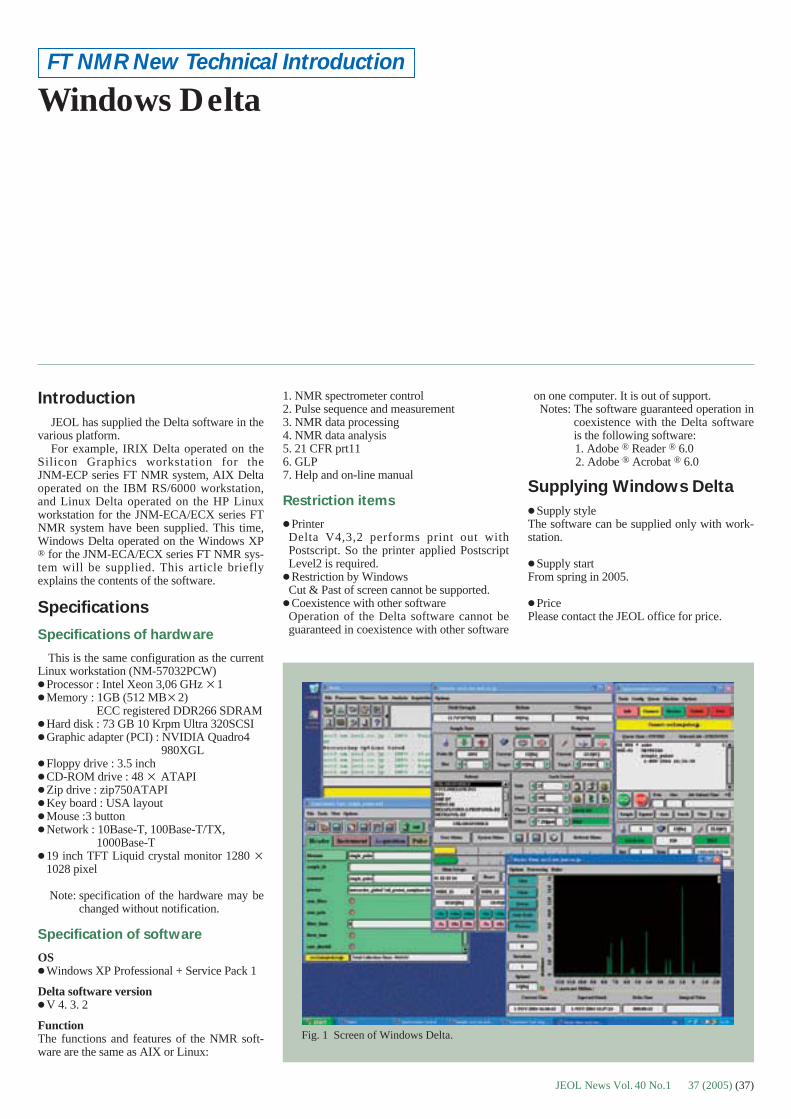
Windows Delta
Introduction
JEOL has supplied the Delta software in thevarious platform.
For example, IRIX Delta operated on theSilicon Graphics workstation for the JNM-ECP series FT NMR system, AIX Deltaoperated on the IBM RS/6000 workstation,and Linux Delta operated on the HP Linuxworkstation for the JNM-ECA/ECX series FTNMR system have been supplied. This time,Windows Delta operated on the Windows XP® for the JNM-ECA/ECX series FT NMR sys-tem will be supplied. This article brieflyexplains the contents of the software.
Specifications
Specifications of hardware
This is the same configuration as the currentLinux workstation (NM-57032PCW)� Processor : Intel Xeon 3,06 GHz �1� Memory : 1GB (512 MB�2)
ECC registered DDR266 SDRAM� Hard disk : 73 GB 10 Krpm Ultra 320SCSI� Graphic adapter (PCI) : NVIDIA Quadro4
980XGL� Floppy drive : 3.5 inch� CD-ROM drive : 48 � ATAPI� Zip drive : zip750ATAPI� Key board : USA layout� Mouse :3 button� Network : 10Base-T, 100Base-T/TX,
1000Base-T� 19 inch TFT Liquid crystal monitor 1280 �
1028 pixel
Note: specification of the hardware may bechanged without notification.
Specification of software
OS� Windows XP Professional + Service Pack 1
Delta software version� V 4. 3. 2
FunctionThe functions and features of the NMR soft-ware are the same as AIX or Linux:
1. NMR spectrometer control2. Pulse sequence and measurement3. NMR data processing4. NMR data analysis5. 21 CFR prt116. GLP7. Help and on-line manual
Restriction items
� PrinterDelta V4,3,2 performs print out withPostscript. So the printer applied PostscriptLevel2 is required.
� Restriction by WindowsCut & Past of screen cannot be supported.
� Coexistence with other softwareOperation of the Delta software cannot beguaranteed in coexistence with other software
on one computer. It is out of support.Notes: The software guaranteed operation in
coexistence with the Delta softwareis the following software:1. Adobe ® Reader ® 6.02. Adobe ® Acrobat ® 6.0
Supplying Windows Delta
� Supply styleThe software can be supplied only with work-station.
� Supply startFrom spring in 2005.
� PricePlease contact the JEOL office for price.
Fig. 1 Screen of Windows Delta.
FT NMR New Technical Introduction
JEOL News Vol. 40 No.1 37 (2005) (37)
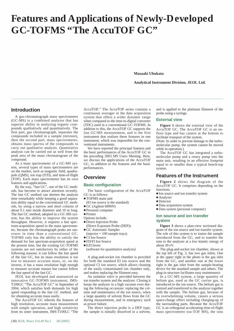
Features and Applications of Newly-DevelopedGC-TOFMS “The AccuTOF GC”
Introduction
A gas-chromatograph mass spectrometer(GC-MS) is a combined analyzer that hassuperior ability in analyzing organic com-pounds qualitatively and quantitatively. Thefirst part, gas chromatograph, separates thecompounds included in a sample (mixture),then the second part, mass spectrometer,obtains mass spectra of the compounds tocarry out qualitative analysis. Quantitativeanalysis can be carried out as well from thepeak area of the mass chromatogram of thecompound.
As a mass spectrometer of a GC-MS sys-tem, several types of mass spectrometers areon the market, such as magnetic field, quadru-pole (QMS), ion trap (ITD), and time-of-flight(TOF). Each mass spectrometer has its ownfeatures and applications.
By the way, “fast GC”, one of the GC meth-ods, has become to attract attention recently.The fast GC method can shorten the analysistime remarkably while keeping a good separa-tion ability equal to the conventional GC meth-ods, by using a narrow and short column ofabout 0.1 mm inside diameter and 10 m long.The fast GC method, adopted in a GC-MS sys-tem, has the ability to improve the systemthroughput. However, it requires a fast spec-trum-acquisition speed to the mass spectrome-ter, because the chromatograph peaks are nar-rower in time than a conventional GC.TOFMS only has the ability to satisfy thedemand for fast spectrum-acquisition speed atthe present time, but the existing GC-TOFMSsystems are not satisfactory by either of thefollowing reasons: it can follow the fast speedof the fast GC, but its mass resolution is toolow to measure accurate mass, or, on theinverse, it has a mass resolution high enoughto measure accurate masses but cannot followthe fast speed of the fast GC.
JEOL has developed and announced aninnovative GC-TOFMS instrument, JMS-T100GC “The AccuTOF GC” in September of2004, which satisfies both demands for highspeed responding to the fast GC method, andfor obtaining accurate mass easily.
The AccuTOF GC inherits the features ofhigh resolution, accurate mass measurementwith simple operation, and high sensitivityfrom its sister instrument, JMS-T100LC “The
AccuTOF.” The AccuTOF series contains acontinuous averager in the data acquisitionsystem that offers a wider dynamic rangewhen compared to the time-to-digital converter(TDC) used in a conventional GC-TOFMS. Inaddition to this, the AccuTOF GC supports thefast GC/MS measurement, and is the firstinstrument that realizes these features in oneinstrument, which was impossible for the con-ventional instruments.
We have reported the principal features andthe basic performances of the AccuTOF GC inthe preceding 2003 MS Users Meeting. Here,we discuss the applications of the AccuTOFGC, in addition to the features and the basicperformances.
Overview
Basic configuration
The basic configuration of the AccuTOFGC is as follows:� TOFMS main unit
(EI ion source is the standard)� GC (Agilent 6890N)� Personal computer� PrinterOptions include:� Direct Injection Probe
(Direct Exposure Probe (DEP))� GC Automatic Sampler
(injector + 100 sample trays)� CI Ion Source� FD/FI Ion Source� EZChrom
(software for quantitative analysis)
A plug-and-socket ion chamber is providedfor both the standard EI ion source and theoptional CI ion source, which allows cleaningof the easily contaminated ion chamber only,and makes replacing the filament easy.
An isolation valve is provided between theion transfer system and the analyzer. Closing itkeeps the analyzer in a high vacuum even dur-ing the following occasions: replacing the col-umn and maintenance of the ion source, whena large quantity of solvent flows from the GCduring measurement, and in emergency suchas power failure.
The direct injection probe is a DEP type;the sample is initially dissolved in a solvent,
and is applied to the platinum filament of theprobe using a syringe.
External view
Figure 1 shows the external view of theAccuTOF GC. The AccuTOF GC is an on-floor type and has casters at the bottom tofacilitate transport of the system.(Note: In order to prevent damage to the turbo-molecular pump, the system cannot be movedwhile in operation.)
The AccuTOF GC has integrated a turbo-molecular pump and a rotary pump into themain unit, resulting in an effective footprintequal to or smaller than a typical bench-topsystem.
Features of the InstrumentFigure 2 shows the diagram of the
AccuTOF GC. It comprises depending on thefunctions:� Ion source and ion transfer system� Analyzer� Detector� Data acquisition system� Data system (personal computer)
Ion source and ion transfer system
Figure 3 shows a plan-view sectioned dia-gram of the ion source and ion transfer system.The role of this system is to ionize the sampleintroduced from the GC, and to transfer theions to the analyzer at a low kinetic energy ofabout 30 eV.
The plug-and-socket ion chamber, shown atthe top left of Fig. 3, has two gas inlets. Oneat the upper right in the photo is the gas inletfrom the GC, and another one at the lowerright is the gas inlet from the sample-heatingdevice for the standard sample and others. Theplug-in structure facilitates easy maintenance.
In a GC-MS system, a large quantity ofhelium gas, used as the GC carrier gas, isintroduced to the ion source. The helium gas isionized and transferred to the analyzer togetherwith the sample. The helium gas, because ofits overwhelming volume, causes a seriousspace-charge effect including charging-up ofthe surrounding parts. Because the AccuTOFGC is an orthogonal accelerating time-of-flightmass spectrometer (oa-TOF MS), the ions
Masaaki Ubukata
Analytical Instrument Division, JEOL Ltd.
(38) JEOL News Vol.40 No.1 38 (2005)

NN
SS
1 2 3
must be transferred at a low kinetic energy ofabout 30 eV to the analyzer. Therefore, theions are highly susceptible to the space-chargeeffect. Moreover, as all the ions, includinghelium ions, introduced to the analyzer reachthe detector, the large quantity of helium ionsmight lead to a failure of the detector. To avoidthe problem, the AccuTOF GC specificallydeveloped an ion-transfer system that canremove more than 99% of helium ions beforethe ions enter the analyzer. The ion transfersystem has the following three structural fea-tures:� The electrostatic lens 2 is separated into two
parts.� An intermediate slit is installed. � A deflector behind the intermediate slit.
In the EI ion source, a source magnet isplaced to prevent dispersion of the electronbeam emitted from the filament. By arrangingthe source magnet in a horizontal plane, anionized ion accepts a force so that it is deflect-ed downward, in case of a positive ion, whilemoving toward the analyzer. The extent ofdeflection differs according to the mass; thesmaller the mass-to-charge ratio, the larger thedeflection. The AccuTOF GC, making use ofthis mass selection ability of the source mag-net, succeeded in colliding the helium ionswith the plate of the intermediate slit andremove them, by optimizing the balance of thevoltages of the upper and lower parts of the
electrostatic lens 2. The intermediate slit alsoassists the differential evacuation between theion source and the analyzer. The ions passedthrough the intermediate slit are introduced tothe analyzer with good efficiency due to theoptimized deflector voltage.
In addition, the AccuTOF GC incorporatesan isolation valve that isolates the ion transfersystem from the analyzer. The isolation valvemakes it possible to vent the ion source andcarry out maintenance of it without venting theanalyzer. Furthermore, it isolates the analyzerautomatically in an emergency such as anunexpected stop of the evacuation system,which prevents the detector from degrading.
Analyzer
The analyzer of the AccuTOF GC is anorthogonal accelerating time-of-flight massspectrometer (oa-TOF MS) incorporating two-stage acceleration and a single-stage reflectron.It achieves high resolution owing to the spatialfocusing by the two-stage acceleration and theenergy focusing by the single-stage reflectron.
The diagram of analyzer of the AccuTOFGC is shown in Fig. 4. The sample is ionizedin the ion source continuously, arranged in aparallel ion beam, and introduced to the spacebetween the push-out plate and the grid 1 (G 1)in the orthogonal accelerator. To accelerateions to the orthogonal direction, pulse volt-
ages, Vpush and Vpull, are applied at the push-out plate and the grid 2 (G 2) respectively.A negative high voltage, Vflight-tube, is appliedat the grid 3 (G 3) and the shield surroundingthe field free region all the time, in case ofanalyzing positive ions. A positive voltage,Vreflectron, is always applied at the end of thereflectron.
Detector
As we will see in the section “ Data acqui-sition system,” when a time-to-digital convert-er (TDC) is used as the data acquisition sys-tem, the quality of a mass spectrum is hardlyaffected by the characteristics of the dataacquisition system. But the TDC system is dif-ficult to handle because it requires statisticalcorrection of the acquired signal, and the massaccuracy depends on the accuracy of theparameter for the statistical correction. On theother hand, when a high-speed analog-to-digi-tal converter (ADC) in combination with acontinuous averager is used as the data acqui-sition system, the quality of a mass spectrum,such as mass resolution and peak shape, isdirectly affected by the characteristics of thedata acquisition system, but this system has amerit that it does not require the statistical cor-rection essentially. The AccuTOF GC adoptsthe ADC-with-continuous averager method,and a device to minimize the signal distortion
Fig. 1 External view of the AccuTOF GC (Includesan optional automatic sampler).
Fig. 2 Diagram of the AccuTOF GC.
Fig. 3 Ion transfer system diagram.
Fig. 4 Analyzer diagram.
Ion source and iontransfer system
Dataacquisitionsystem
Analyzer
Detector
RP 1 RP 2
TMP 1 TMP 2
Intermediateslit
Sourcemagnet
Plug-and-socketion chamber
Isolationvalve
Deflector
TOF MS
Electrostatic lenses
Sample ion
Helium ion
Spatial focusing
Energy focusing
JEOL News Vol. 40 No.1 39 (2005) (39)
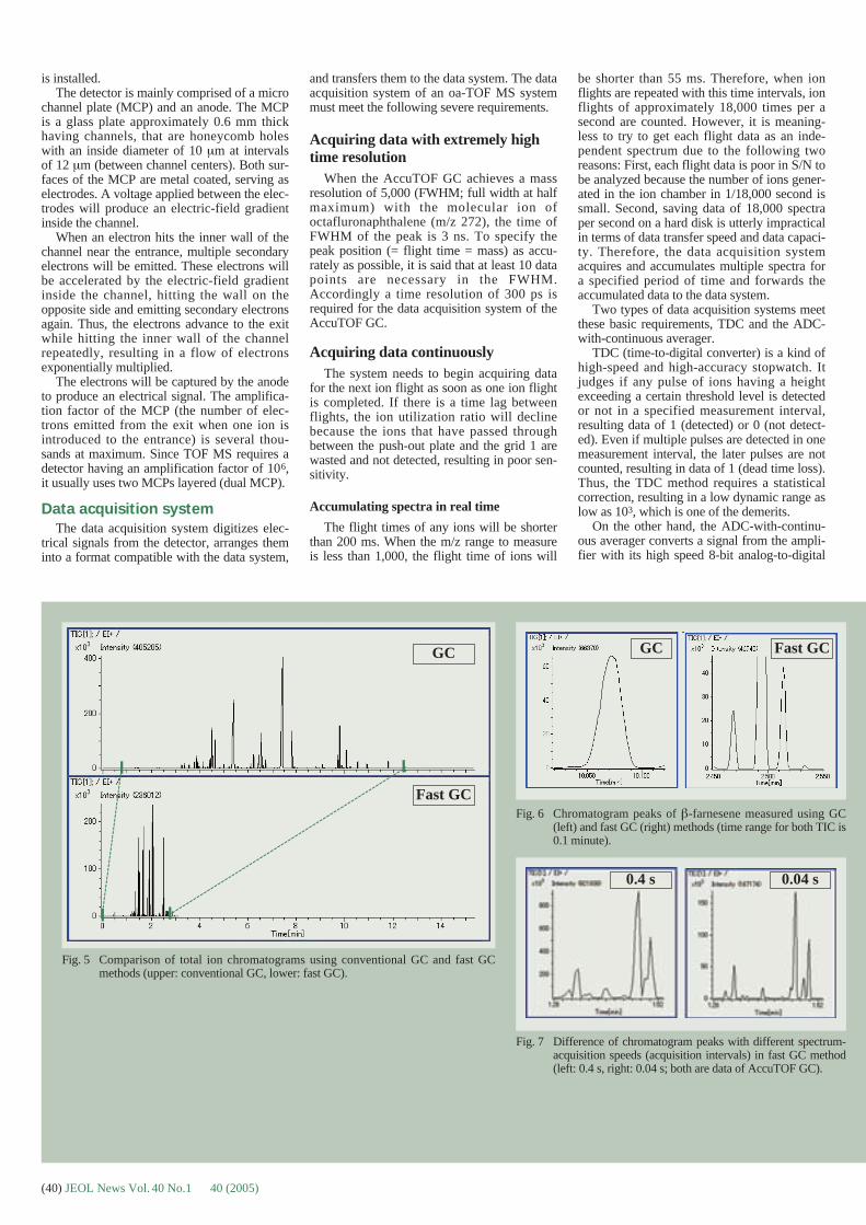
(40) JEOL News Vol. 40 No.1 40 (2005)
is installed.The detector is mainly comprised of a micro
channel plate (MCP) and an anode. The MCPis a glass plate approximately 0.6 mm thickhaving channels, that are honeycomb holeswith an inside diameter of 10 µm at intervalsof 12 µm (between channel centers). Both sur-faces of the MCP are metal coated, serving aselectrodes. A voltage applied between the elec-trodes will produce an electric-field gradientinside the channel.
When an electron hits the inner wall of thechannel near the entrance, multiple secondaryelectrons will be emitted. These electrons willbe accelerated by the electric-field gradientinside the channel, hitting the wall on theopposite side and emitting secondary electronsagain. Thus, the electrons advance to the exitwhile hitting the inner wall of the channelrepeatedly, resulting in a flow of electronsexponentially multiplied.
The electrons will be captured by the anodeto produce an electrical signal. The amplifica-tion factor of the MCP (the number of elec-trons emitted from the exit when one ion isintroduced to the entrance) is several thou-sands at maximum. Since TOF MS requires adetector having an amplification factor of 106,it usually uses two MCPs layered (dual MCP).
Data acquisition system
The data acquisition system digitizes elec-trical signals from the detector, arranges theminto a format compatible with the data system,
and transfers them to the data system. The dataacquisition system of an oa-TOF MS systemmust meet the following severe requirements.
Acquiring data with extremely hightime resolution
When the AccuTOF GC achieves a massresolution of 5,000 (FWHM; full width at halfmaximum) with the molecular ion ofoctafluronaphthalene (m/z 272), the time ofFWHM of the peak is 3 ns. To specify thepeak position (= flight time = mass) as accu-rately as possible, it is said that at least 10 datapoints are necessary in the FWHM.Accordingly a time resolution of 300 ps isrequired for the data acquisition system of theAccuTOF GC.
Acquiring data continuouslyThe system needs to begin acquiring data
for the next ion flight as soon as one ion flightis completed. If there is a time lag betweenflights, the ion utilization ratio will declinebecause the ions that have passed throughbetween the push-out plate and the grid 1 arewasted and not detected, resulting in poor sen-sitivity.
Accumulating spectra in real time
The flight times of any ions will be shorterthan 200 ms. When the m/z range to measureis less than 1,000, the flight time of ions will
Fig. 5 Comparison of total ion chromatograms using conventional GC and fast GCmethods (upper: conventional GC, lower: fast GC).
Fig. 6 Chromatogram peaks of -farnesene measured using GC(left) and fast GC (right) methods (time range for both TIC is0.1 minute).
be shorter than 55 ms. Therefore, when ionflights are repeated with this time intervals, ionflights of approximately 18,000 times per asecond are counted. However, it is meaning-less to try to get each flight data as an inde-pendent spectrum due to the following tworeasons: First, each flight data is poor in S/N tobe analyzed because the number of ions gener-ated in the ion chamber in 1/18,000 second issmall. Second, saving data of 18,000 spectraper second on a hard disk is utterly impracticalin terms of data transfer speed and data capaci-ty. Therefore, the data acquisition systemacquires and accumulates multiple spectra fora specified period of time and forwards theaccumulated data to the data system.
Two types of data acquisition systems meetthese basic requirements, TDC and the ADC-with-continuous averager.
TDC (time-to-digital converter) is a kind ofhigh-speed and high-accuracy stopwatch. Itjudges if any pulse of ions having a heightexceeding a certain threshold level is detectedor not in a specified measurement interval,resulting data of 1 (detected) or 0 (not detect-ed). Even if multiple pulses are detected in onemeasurement interval, the later pulses are notcounted, resulting in data of 1 (dead time loss).Thus, the TDC method requires a statisticalcorrection, resulting in a low dynamic range aslow as 103, which is one of the demerits.
On the other hand, the ADC-with-continu-ous averager converts a signal from the ampli-fier with its high speed 8-bit analog-to-digital
Fig. 7 Difference of chromatogram peaks with different spectrum-acquisition speeds (acquisition intervals) in fast GC method(left: 0.4 s, right: 0.04 s; both are data of AccuTOF GC).
GC
Fast GC
GC Fast GC
0.4 s 0.04 s

JEOL News Vol. 40 No.1 41 (2005) (41)
converter (ADC) to a digital value of 0 to 255(= 28-1), and the data are accumulated in thesumming memory. Therefore, the ADC-with-continuous averager basically does not need astatistical correction.
The AccuTOF GC adopts an ADC-with-continuous averager in the data acquisitionsystem.
Basic Performance
The basic performance of the AccuTOF GCis as follows.� Resolution: 5,000 or more
(FWHM, PFK m/z293)� Mass range: 4 to 2,000� Sensitivity
EI+ mode: S/N�100,Octafluoronaphthalene, 1 pg(mass chromatogram of m/z 272,RMS)
CI+ mode: S/N�150, Benzophenone, 100 pg(mass chromatogram of m/z 183,RMS)Isobutane: 0.1 mL/min
CI- mode: S/N�20,Hexachlorobenzene, 100 fg(mass chromatogram of m/z 284, RMS)Methane: 1.0 mL/min
GC conditions:Column: Agilent Technologies, DB-5ms
0.25 mm (inside diameter) �30 m(length), 0.25 µm (film thickness)
Flow rate: Helium 1.0 mL/min (constant flow)
� Spectrum-acquisition speed: 0.04 s or longer(25 spectra/s or smaller)
� Mass accuracy: 2 mmu or 5 ppm (RMS, internal standard)
The AccuTOF GC has the features of highresolution, accurate mass measurement witheasy operation, and high sensitivity as same asits sister instrument, JMS-T100LC “TheAccuTOF.” The AccuTOF GC furthermoreattains a high spectrum-acquisition speed of 25spectra per second, and fully corresponds tothe fast GC/MS measurement.
We show data regarding the basic perform-ance below, that are: fast GC/MS measure-ment, accurate mass measurement, stability,and dynamic range.
Fast GC/MS measurement
As an example of the fast GC/MS measure-ment, an essential oil of lavender is measured.Here, we discuss the differences between theconventional GC and the fast GC methods, andthe high spectrum-acquisition speed requiredfor the fast GC/MS method. These two pointsare described briefly.
What is fast GC method?The fast GC method uses a narrow and
short column, which shortens the analysis timewhile retaining a high-separation ability equiv-
alent to a conventional GC method.An essential oil of lavender is measured
using the AccuTOF GC with the conventionalGC method, and also with the fast GC method,and the results are compared.
� GC parameters� Sample injection: Split (1:500)� Sample injection volume: 0.2 µL� Oven program:70°C (0.5 min) �<ramp rate:
10 °C/min> � 250°C (3 min)� Column: DB-5ms,0.25 mm (inside diameter)
�30 m (length), 0.25 µm (film thickness)
� Fast GC parameters� Sample injection: Split (1:500)� Sample injection volume: 0.2 µL� Oven program: 70°C (0.5 min)�<ramp rate:
60°C/min> � 250 °C (3 min)� Column:BPX-5, 0.1 mm (inside diameter)
�10 m (length), 0.1 µm (film thickness)
� MS parameters� Mass measurement range: m/z 35 to 300� Spectrum-acquisition speed: 0.04 s
(25 spectra/s)
The parameters for GC and the fast GC dif-fers in two points; column type and oven-tem-perature ramp rate. The fast GC uses a narrowand short column of 0.1 mm inside diameterand 10 m long, and the oven-temperature ramp
Sample Theoretical Measured Error concentration m/z m/z (mmu)
3pg 281.81312 281.81233 � 0.7910pg 281.81180 � 1.3230pg 281.81196 � 1.16
100pg 281.81211 � 1.01300pg 281.81160 � 1.52
1ng 281.81153 � 1.592ng 281.81214 � 0.98
Fig. 8 Structural diagram of hexachlorobenzene(C6Cl6).
Table 1 Measured masses of hexachlorobenzene with different concentrationsare compared with the theoretical mass.
Fig. 9 Mass spectrum of mixture of PFK and hexachlorobenzene (2 ng).
Fig. 10 Structural diagram of octafluoronaph-thalene (C10F8).
Fig. 11 Stability of sensitivity and resolution during the 45-hour continu-ous measurement. Sample: octafluoronaphthalene.
Fig. 12 Mass chromatograms of m/z 272 when starting (left) and 45 hourslater (right).
HCB m/z282
PFK m/z219
S/N : 127 S/N : 134
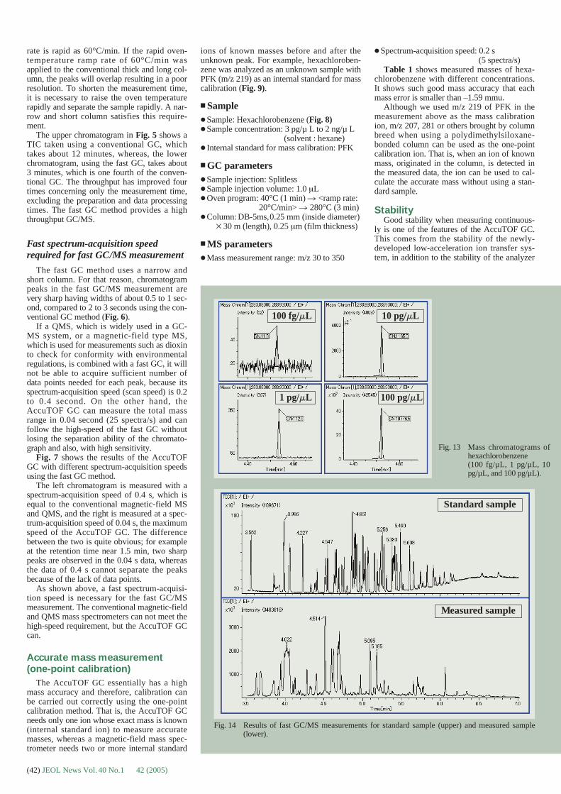
(42) JEOL News Vol. 40 No.1 42 (2005)
rate is rapid as 60°C/min. If the rapid oven-temperature ramp rate of 60°C/min wasapplied to the conventional thick and long col-umn, the peaks will overlap resulting in a poorresolution. To shorten the measurement time,it is necessary to raise the oven temperaturerapidly and separate the sample rapidly. A nar-row and short column satisfies this require-ment.
The upper chromatogram in Fig. 5 shows aTIC taken using a conventional GC, whichtakes about 12 minutes, whereas, the lowerchromatogram, using the fast GC, takes about3 minutes, which is one fourth of the conven-tional GC. The throughput has improved fourtimes concerning only the measurement time,excluding the preparation and data processingtimes. The fast GC method provides a highthroughput GC/MS.
Fast spectrum-acquisition speedrequired for fast GC/MS measurement
The fast GC method uses a narrow andshort column. For that reason, chromatogrampeaks in the fast GC/MS measurement arevery sharp having widths of about 0.5 to 1 sec-ond, compared to 2 to 3 seconds using the con-ventional GC method (Fig. 6).
If a QMS, which is widely used in a GC-MS system, or a magnetic-field type MS,which is used for measurements such as dioxinto check for conformity with environmentalregulations, is combined with a fast GC, it willnot be able to acquire sufficient number ofdata points needed for each peak, because itsspectrum-acquisition speed (scan speed) is 0.2to 0.4 second. On the other hand, theAccuTOF GC can measure the total massrange in 0.04 second (25 spectra/s) and canfollow the high-speed of the fast GC withoutlosing the separation ability of the chromato-graph and also, with high sensitivity.
Fig. 7 shows the results of the AccuTOFGC with different spectrum-acquisition speedsusing the fast GC method.
The left chromatogram is measured with aspectrum-acquisition speed of 0.4 s, which isequal to the conventional magnetic-field MSand QMS, and the right is measured at a spec-trum-acquisition speed of 0.04 s, the maximumspeed of the AccuTOF GC. The differencebetween the two is quite obvious; for exampleat the retention time near 1.5 min, two sharppeaks are observed in the 0.04 s data, whereasthe data of 0.4 s cannot separate the peaksbecause of the lack of data points.
As shown above, a fast spectrum-acquisi-tion speed is necessary for the fast GC/MSmeasurement. The conventional magnetic-fieldand QMS mass spectrometers can not meet thehigh-speed requirement, but the AccuTOF GCcan.
Accurate mass measurement(one-point calibration)
The AccuTOF GC essentially has a highmass accuracy and therefore, calibration canbe carried out correctly using the one-pointcalibration method. That is, the AccuTOF GCneeds only one ion whose exact mass is known(internal standard ion) to measure accuratemasses, whereas a magnetic-field mass spec-trometer needs two or more internal standard
ions of known masses before and after theunknown peak. For example, hexachloroben-zene was analyzed as an unknown sample withPFK (m/z 219) as an internal standard for masscalibration (Fig. 9).
� Sample� Sample: Hexachlorobenzene (Fig. 8)� Sample concentration: 3 pg/µ L to 2 ng/µ L
(solvent : hexane)� Internal standard for mass calibration: PFK
� GC parameters� Sample injection: Splitless� Sample injection volume: 1.0 µL� Oven program: 40°C (1 min) � <ramp rate:
20°C/min> � 280°C (3 min)� Column: DB-5ms,0.25 mm (inside diameter)
�30 m (length), 0.25 µm (film thickness)
� MS parameters� Mass measurement range: m/z 30 to 350
� Spectrum-acquisition speed: 0.2 s (5 spectra/s)
Table 1 shows measured masses of hexa-chlorobenzene with different concentrations.It shows such good mass accuracy that eachmass error is smaller than –1.59 mmu.
Although we used m/z 219 of PFK in themeasurement above as the mass calibrationion, m/z 207, 281 or others brought by columnbreed when using a polydimethylsiloxane-bonded column can be used as the one-pointcalibration ion. That is, when an ion of knownmass, originated in the column, is detected inthe measured data, the ion can be used to cal-culate the accurate mass without using a stan-dard sample.
StabilityGood stability when measuring continuous-
ly is one of the features of the AccuTOF GC.This comes from the stability of the newly-developed low-acceleration ion transfer sys-tem, in addition to the stability of the analyzer
Fig. 13 Mass chromatograms ofhexachlorobenzene(100 fg/µL, 1 pg/µL, 10pg/µL, and 100 pg/µL).
Fig. 14 Results of fast GC/MS measurements for standard sample (upper) and measured sample(lower).
100 fg/�L 10 pg/�L
1 pg/�L 100 pg/�L
Standard sample
Measured sample
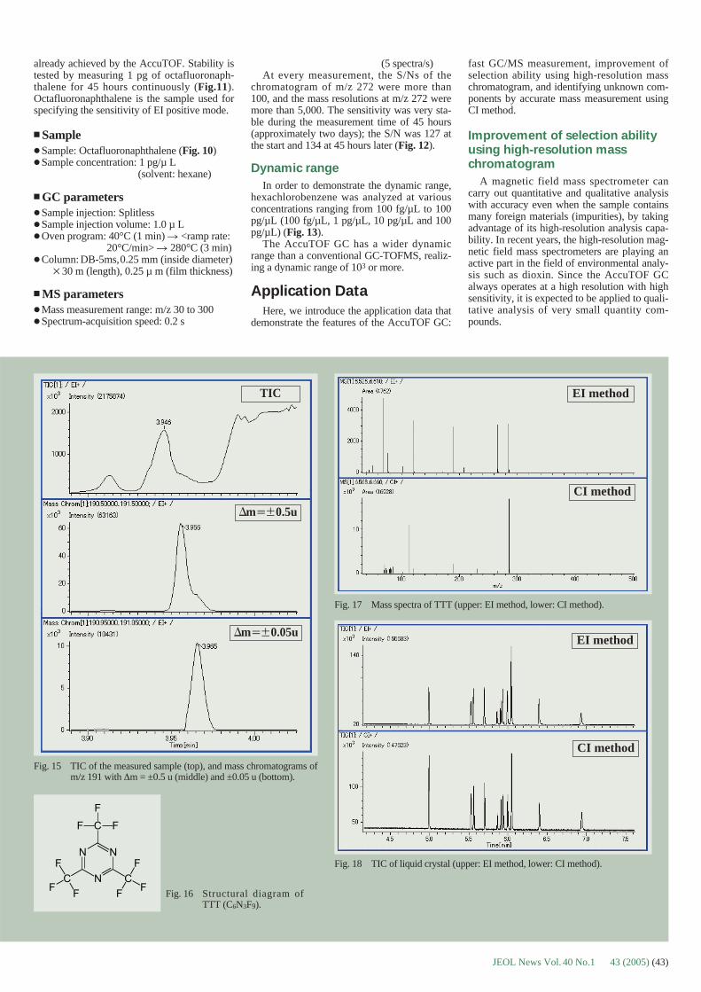
JEOL News Vol. 40 No.1 43 (2005) (43)
already achieved by the AccuTOF. Stability istested by measuring 1 pg of octafluoronaph-thalene for 45 hours continuously (Fig.11).Octafluoronaphthalene is the sample used forspecifying the sensitivity of EI positive mode.
� Sample� Sample: Octafluoronaphthalene (Fig. 10)� Sample concentration: 1 pg/µ L
(solvent: hexane)
� GC parameters� Sample injection: Splitless� Sample injection volume: 1.0 µ L� Oven program: 40°C (1 min) � <ramp rate:
20°C/min> � 280°C (3 min)� Column: DB-5ms,0.25 mm (inside diameter)
�30 m (length), 0.25 µ m (film thickness)
� MS parameters� Mass measurement range: m/z 30 to 300� Spectrum-acquisition speed: 0.2 s
(5 spectra/s)At every measurement, the S/Ns of the
chromatogram of m/z 272 were more than100, and the mass resolutions at m/z 272 weremore than 5,000. The sensitivity was very sta-ble during the measurement time of 45 hours(approximately two days); the S/N was 127 atthe start and 134 at 45 hours later (Fig. 12).
Dynamic range
In order to demonstrate the dynamic range,hexachlorobenzene was analyzed at variousconcentrations ranging from 100 fg/µL to 100pg/µL (100 fg/µL, 1 pg/µL, 10 pg/µL and 100pg/µL) (Fig. 13).
The AccuTOF GC has a wider dynamicrange than a conventional GC-TOFMS, realiz-ing a dynamic range of 103 or more.
Application Data
Here, we introduce the application data thatdemonstrate the features of the AccuTOF GC:
fast GC/MS measurement, improvement ofselection ability using high-resolution masschromatogram, and identifying unknown com-ponents by accurate mass measurement usingCI method.
Improvement of selection abilityusing high-resolution mass chromatogram
A magnetic field mass spectrometer cancarry out quantitative and qualitative analysiswith accuracy even when the sample containsmany foreign materials (impurities), by takingadvantage of its high-resolution analysis capa-bility. In recent years, the high-resolution mag-netic field mass spectrometers are playing anactive part in the field of environmental analy-sis such as dioxin. Since the AccuTOF GCalways operates at a high resolution with highsensitivity, it is expected to be applied to quali-tative analysis of very small quantity com-pounds.
Fig. 17 Mass spectra of TTT (upper: EI method, lower: CI method).
EI method
CI method
Fig. 18 TIC of liquid crystal (upper: EI method, lower: CI method).
EI method
CI methodFig. 15 TIC of the measured sample (top), and mass chromatograms of
m/z 191 with m = ±0.5 u (middle) and ±0.05 u (bottom).
�
�
�
�
�
��
�
�
�
��
�
�
�Fig. 16 Structural diagram of
TTT (C6N3F9).
TIC
m�0.5u
m�0.05u

(44) JEOL News Vol. 40 No.1 44 (2005)
Fig. 19 Mass spectra of compound A(upper: EI method, lower: CI method).
EI method
CI method
Fig. 21 Estimated structure of compound B.
Table 4 Estimated formula for each ion of compound B observed by EI method.
Ion Measured Theoretical Error Estimated Unsaturation m/z m/z (mmu) formula number
m/z 333 333.17432 333.17288 1.44 C22H23NO2 12
m/z 195 195.06891 195.06841 0.5 C13H9NO 10
m/z 111 111.11872 111.11738 1.34 C8H15 1.5
m/z 69 69.07042 69.07042 1.09 C6H9 1.5
Candidate Measured Theoretical Error Estimated Unsaturationm/z m/z (mmu) formula number
No.1 334.18021 334.18070 �0.49 C22H24NO2 11.5
No.2 334.18185 �1.64 C19H25FNO3 7.5
Table 3 Composition estimation result of [M+H]+ in compound B.
Fig. 20 Mass spectra of compound B (upper: EI method, lower: CI method).
EI method
CI method
In order to verify mass separation of a targetcompound from a sample containing manyforeign materials using a high-resolution masschromatogram, we added a standard sample,which includes 68 pesticides, into the extractfrom food, and verified that the compoundscan be detected as a peak in a mass chro-matogram. Measurement conditions andresults are presented below.
� Sample� Standard sample: Includes 68 pesticides.� Standard sample concentration: 50 pg/µ L
(solvent: hexane)� Measured sample: Blank (extract from food)
+ standard sample
� Fast GC parameters� Sample injection: Splitless� Sample injection volume: 1.0 µL� Oven program: 40°C (1 min) � <ramp rate:
50°C/min> � 300°C (1 min)� Column: DB-5, 0.18 mm (inside diameter)
�10 m (length) �0.18 µ m (film thickness)
� MS parameters
� Mass measurement range: m/z 30 to 500� Spectrum-acquisition speed: 0.04 s
(25 spectra/s)
Figure14 shows the TICs of the standardsample (upper) and the measured sample(lower). The measured sample is prepared byspiking 50 pg of standard sample into theblank (extract from food). The standard sample(upper) is clearly separated, and we couldidentify each pesticide even in the TIC.However, it is difficult to identify the standardsample in the TIC of the measured sample(lower), because the measured sample containsmany foreign materials.
In the AccuTOF GC, when you create amass chromatogram from measured data, amass range (window width) must be specified.That is, if a wide mass range is specified, alow-resolution mass chromatogram equivalentto the conventional low-resolution measure-ment is obtained. On the other hand, if a nar-row mass range is specified, a high-resolutionmass chromatogram is obtained.
We examined what kind of mass chro-matograms are obtained when we give twowindow width values, m = ±0.5 u and ±0.05u, to the base peak of Chloroneb, [M-CH3]+
(m/z 191), which is one of the 68 pesticides(Fig. 15).
In the TIC (top), the intense background isobserved, and the chromatogram is broad anddull. In the mass chromatogram with the win-dow width m = ±0.5 u (middle), a peak wasobserved at a retention time of 3.956 minutes.However, searching for this spectrum using theNIST library database identified that the com-pound is most possibly 2, 4-Di-tert-butylphe-nol, a different material from the spiked 68pesticides. Next, in the mass chromatogramwith the window width m = ±0.05 u (bot-tom), a peak was observed at a retention timeof 3.965 minutes. This peak was identified tobe chloroneb using the NIST library database.
Thus, when we create a low-resolution masschromatogram ( m = ±0.5 u, equivalent toQMS), it was difficult to find the compoundsburied in the foreign materials; however, thehigh-resolution mass chromatogram ( m =±0.05 u) enabled the identification of the com-
Ionization method Ion Theoretical Measured Errorm/z m/z (mmu)
EI method [M�CH3]� 192.08132 192.08230 0.98
[M]� 207.10480 207.10589 1.09
CI method [M�H]� 208.11262 208.11367 1.05
Table 2 Calculated accurate mass of each ion.

JEOL News Vol. 40 No.1 45 (2005) (45)
pound.In addition, we mention that the fast
GC/MS measurement took only about six min-utes to detect the 68 pesticides. It will takeabout thirty minutes for a conventionalGC/MS measurement, demonstrating improve-ment of the throughput about five times.
Identifying unknown compoundsby accurate mass measurementusing CI method
The process of the CI method is as follows:First, the reagent gas, for example, methane orisobutene, is introduced into a closed ioniza-tion chamber, and the reagent gas is ionized bythe EI method. Next, the sample is introducedfrom the sample injection section (a GC orstandard-sample injection section) into the ion-ization chamber. There, an ion-molecule reac-tion takes place between the reagent gas ionsand the sample molecules resulting in the ion-ization of the sample.
The CI method is a soft ionization methodcompared to the EI method, and offers usefulinformation for determining the molecularmass of unknown sample. As the reagent gas,methane, isobutene or ammonia is mainlyused. Ions [M+H]+ are mainly observed whenusing the former two gases, and [M+NH4]+
ions when using ammonia gas.In the present experiment, we carried out a
measurement that combines the CI method and“simple and accurate mass measurement”, oneof the features of the AccuTOF GC.
� Sample� Sample: Liquid crystal in a commercially
available pocket calculator was dissolved in a solvent (hexane).
� Internal standard compound: 2, 4, 6-Tris (trifluoromethyl)-1, 3, 5-triazine (abbreviated to TTT, Fig. 16)
� Fast GC parameters� Sample injection: Split (1:400 (EI method),
1:200 (CI method)� Sample injection volume:1.0 µ L� Oven program: 40°C (1 min) � <ramp rate:
50°C /min> � 300°C (1 min)� Column: DB-5, 0.18 mm (inside diameter)
�10 m (length) �0.18 µ m (film thickness)
� MS parameters� Measurement mass range: m/z 70 to 500� Spectrum-acquisition speed: 0.04 s
(25 spectra/s)
� CI parameters� CI reagent gas: Isobutane� Flow rate of CI reagent gas: 0.1 mL/min
(controlled by mass-flow controller)
Figure 17 shows the mass spectra of TTT,the internal standard compound, obtainedusing EI (upper) and CI (lower) methods.
The TTT can be ionized by the CI methodsince it contains many nitrogen atoms, as wellas by the EI method. Figure 17 indicates that[M]+ is obtained by the EI method and[M+H]+ by the CI method with good sensitivi-ty. The accurate masses are calculated by one-point calibration using these ions. The meas-ured data are shown below.
Figure 18 shows very sharp peaks since theinjection method “split” is used in both EI andCI methods. To show an example of identifica-tion analysis, we selected the first peak A(compound A) at the retention time around 5.0min and the last peak B (compound B) at theretention time around 7.0 min.
On the upper mass spectrum in Fig. 19,compound A by EI method, m/z 192 isobserved as the base peak and the next intensepeak is m/z 207. The lower mass spectrum inthe figure, compound A by CI method, showsbase peak of m/z 208. Therefore, it is inferredthat m/z 207 ion observed using the EI methodis the molecular ion of the compound A. Themass spectrum obtained by the EI method issearched for using the NIST library database,resulting in a compound with molecular massof 207 as the first candidate (match: 912), thatis, (1, 1’-Biphenyl)-4-carbonitrile, 4’-ethyl-(C15H13N). As the next step, one-point calibra-tion is carried out to calculate the accuratemass of it using TTT, the internal standardcompound.
Accurate masses are calculated from thepredicted structures of each ion (Table 2). Asa result, measured values have mass errors ofabout 1 mmu from the theoretical values,showing very good accuracy. Thus, the com-pound A is determined to be (1, 1’-Biphenyl)-4-carbonitrile, 4’-ethyl- using the NIST librarydatabase search and the calculated accuratemasses by using the EI and CI methods.
Next, the compound B is analyzed and dis-cussed below. The obtained mass spectra areshown in Fig. 20.
On the upper mass spectrum in Fig. 20,compound B by EI method, m/z 111 isobserved as the base peak, and m/z 69 and 195as successive peaks. The lower mass spectrumin the figure (compound B by CI method)shows base peak of m/z 334. In the upper massspectrum by EI, a small peak is observed atm/z 333. Therefore, it is inferred that m/z 333is the molecular ion of the compound B.However, when we searched for the massspectrum obtained by the EI method using theNIST library database, even the spectrum pat-tern of the first-candidate compound could notagree (match: 557). In addition, its molecularmass was not 333. Furthermore, other candi-dates did not have a molecular mass of 333.Thus, from the viewpoints of spectrum patternand molecular mass, it is considered that thereis a high possibility that this compound is notregistered in the NIST library database. Inorder to find this unknown compound, we cal-culated accurate masses of each ion and esti-mated the composition.
Since the molecular mass of this compoundis estimated to be 333, an odd number, it isconsidered, from the nitrogen rule, that thenumber of nitrogen atoms contained is odd. Inthe present study, estimation was carried outby aiming and estimating element species andtheir numbers, taking the representative liquid-crystal families into account [1]. Table 3shows the result of the composition estimationby deducing from the accurate mass of m/z334 in the mass spectrum obtained by the CImethod. In estimating composition, the calcu-lation was carried out with an error of 2 mmuor less.
When we consider the composition of can-didate No. 2 from the compounds of the repre-
sentative liquid-crystal families, compoundshaving three oxygen atoms are narrowed downto azoxy compounds and p-cyano-phenyl-estercompounds of p-alkyl substitution benzoicacid. But, among these compounds, not onecontaining a fluorine atom has been reported[1]. From these facts, the composition of com-pound B is possibly and surely must be No. 1.We estimated the structure from the composi-tion formula of No. 1 (C22H24NO2) and thefragment pattern obtained by the EI method.First, we estimated the composition formulafrom the accurate masses of the ions obtainedby the EI method. Table 4 shows the results.
The candidate No. 1 contains one nitrogenatom, but it is known that there is no com-pound having an amino group (-NH2) or anitro group (-NO2) in the liquid-crystal fami-lies. From this fact, it is estimated that thenitrogen atom in the candidate No. 1 exists inthe form of a cyano group (-CN). The candi-date No. 1 also includes two oxygen atoms andthey are estimated to form an ester. In addition,since the unsaturation number of [M]+ istwelve, it is estimated that at least one or twobenzene nuclei are included. As a result, twostructures are deduced and shown in Fig. 21,that are p-cyanophenylester and cyclohexa-necarboxylic acid aryl ester substitution prod-uct.
It is considered that m/z 111 is formed by asimple cleavage of an alkyl group, and m/z 69is formed accompanying hydrogen transfer ina cyclohexane ring. These two ions can begenerated from either structures [I] and [II].However the ion m/z 195 is difficult to createfrom structure [II], and is deduced to arisefrom a simple cleavage of an alkoxy groupaccompanying hydrogen transfer in structure[I]. As a conclusion, the structure of the com-pound B is suggested to be structure [I] fromthe fragment ions obtained by the EI method.
Conclusion
In the present paper, we introduced the fea-tures of the AccuTOF GC and its applications,including fast GC/MS measurement, accuratemass measurement, and improvement of selec-tion ability using high-resolution mass chro-matogram. In particular, it was demonstratedthat measuring accurate masses using the EIand CI methods allows structural and qualita-tive analysis of the target compound with highreliability.
JMS-T100GC, the AccuTOF GC, is aninnovative GC-MS that succeeds in obtainingthe features that were impossible to attainsimultaneously using conventional instru-ments. The features are: fast spectrum-acquisi-tion speed that deals the fast GC/MS data,accurate mass measurement with simple oper-ation, and stable, high sensitivity.
We hope the AccuTOF GC will help you inyour research and studies.
References
[1] Liquid Crystal Compound Glossary, ed.Japan Society for the Promotion ofScience, Baifukan Co., Ltd, Tokyo (inJapanese)
Introduction of Wafer Edge SEM Review
Tomohiro Mihira
Semiconductor Equipment Division, JEOL Ltd.
Introduction
Wafer edge problems are beginning to bepointed out with progress in larger-diametersilicon wafers and practical use of 300 mmwafers.
There are two problems of wafer edges. Thefirst is wafer cracks that have come to be seri-ous with the employment of 300 mm wafers.
A wafer crack not only wastes a wafer thatcame through the semiconductor productionprocesses, but also causes a large downtime inthe production equipment because the wafercracks in the equipment. A crack in the waferedge leads to a crack of the entire wafer. Thatis, if the wafer has a crack in the edge, as thestress applied to a wafer increases in manyproduction processes, the wafer cracks.
The second problem is yield degradationdue to dust generated from the wafer edge.
As the device production process proceeds,deposition and peeling-off of insulating andmetallic films results in contamination, parti-cles adhering to the wafer and scratches on it.The resultant particles come around on thewafer surface and they cause a “killer defect”.In addition, as the wafer diameter increases,the number of chips on the wafer surface alsoincreases, together with the increase in thenumber of chips on the periphery of the wafer.The chips near the periphery are easily affect-ed by particles peeled off from the edge, andthe dust from the edge greatly degrades theyield. Furthermore, in the process where depo-sition is applied to the entire wafer surface,deposited films come around to the lowerbevel of the wafer edge, and this phenomenoncauses contamination in the subsequentprocesses.
Under these problematic circumstances,defect analysis/management of the wafer edge,which previously did not draw attention, isbecoming more important in recent years.
To solve the above problems, JEOL willpropose defect analysis/management of thewafer edge by Wafer Edge SEM Review.
Wafer Edge SEM Review Outline
JEOL DRT-SEMs (defect-review-tool scan-ning electron microscopes), the JWS/JFSseries, have conventionally used tilting/rotat-
ing stages. Also, the JWS/JFS series employ aconical objective lens for higher SEM resolu-tion and a eucentric stage for tilt observation.These features are widely accepted to be veryeffective for defect analysis of wafer surfaces.Recently, these features, particularly tilting/rotating stages, have found also to be effectivefor observation of wafer edges.
The JWS/JFS series can observe wafer sur-faces tilted up to 60°. Observation of the waferedge at 60° allows one to view the lower beveland apex of the edge as well as the wafer sur-face. In addition, since the wafer stage of theJWS/JFS can endlessly rotate over 360° with0.1° step rotational movement, an operator canobserve the entire circumference of the wafer.
Figure 1 shows the observable range of thewafer edge using the JWS/JFS series. As men-tioned above, using the wafer stage of theJWS/JFS, an operator can limitlessly and easi-ly observe a broad range of the wafer edge,illustrated in Fig. 1 (left).
Furthermore, since an optional EDS (ener-gy-dispersive X-ray) detector can be attachedto the instrument, EDS measurement can beperformed for defects on the wafer edge. Inthis way, the JWS/JFS series provide composi-tion analysis of the wafer edge through EDSmeasurement as well as wafer edge observa-tion, thus enabling one to obtain necessaryinformation to be fed back to each productionprocess.
Featuring their wealth of capabilities, theJWS/JFS series are increasingly attractingmuch attention, as powerful tools for waferedge analysis.
New functions
For smooth and easy analysis of waferedges using the JWS/JFS series, JEOL hasdeveloped two new functions (Fig. 2).
Coordinate linkage with Raytex EdgeScan+The coordinate-linkage function has
enabled the JWS/JFS to link with the coordi-nate system of the Raytex EdgeScan+, theindustry-standard, optical wafer edge defect-inspection system.
An optical wafer edge defect-inspectionsystem measures positions where defects arepresent. Using this new function, the JWS/JFSinstruments can concentrate on observing
defect points according to the positional infor-mation measured by a wafer edge defect-inspection system. This capability allows oneto inspect and analyze defects on the wafer-edge with high throughput.
Automatic observation of wafer-edgesThe Auto Edge Review function automati-
cally captures a sequence of SEM images ofthe entire circumference of the wafer edge.Since the images are saved in the computer,after capturing the images, an operator canreview the images and determine the presenceor absence of defects and the defect positions.This function is effective for users who do nothave wafer edge defect-inspection systems.
Application Example of
Wafer Edge SEM ReviewFigure 3 shows an example of Wafer Edge
SEM Review.SEM images in Fig. 3 show that part of the
tungsten (W) film deposited on the wafer edgeis peeled off. It is said that the adhesionbetween the substrate and the deposited film islow, and these SEM images prove this think-ing.
If the peeled-off W film adheres to thewafer surface, this can degrade the yield. TheSEM images suggest that it is necessary to millthe deposited W film before it peels off fromthe wafer edge.
In this way, SEM observation of wafer-edges enables one to take measures for theprocess of the wafer edge, which was not donepreviously.
Summary
JEOL will propose Wafer Edge SEMReview for defect analysis of wafer edges,which is now drawing attention. The waferstage of the JWS/JFS series can tilt over awide range and afford rotational movement,enabling one to easily observe wafer edges.Furthermore, EDS analysis as well as SEMobservation allows one to precisely obtaindetailed information on defects on the waferedge and feed the information back to the pro-duction processes. Thus, Wafer Edge SEMReview will play an important role in yieldimprovement of semiconductor devices.
(50) JEOL News Vol.40 No.1 50 (2005)

Observable range of the wafer edge at a tilt angle of 60°
Light source Wafer cross section SEM image Light source Wafer
�
APEX
Tilt 60°
Fig. 1 Observable range of the wafer edge.
Fig. 2 Effective functions for wafer edge observation.
Fig. 3 Application example of Wafer Edge SEM Review to observation of peeling-off of W film.
Coordinate linkage with wafer-edge defect-inspection system Auto Edge Review function
Sequence of SEM images of wafer edge
(c) Enlarged view around point 1 in(b)
(d) Enlarged view around point 2 in(b)
(b) Enlarged view of the positioncircled in (a). (e) EDS spectra of Si and SiO2 (sub-
strate components) obtainedfrom points 3 (upper) and 4(lower) in (b).
(a) W film peeled off from the waferedge (wide field of view)
Observable range of the wafer edge over 360° rotation
JEOL News Vol. 40 No.1 51 (2005) (51)
1
4 3
2
c)a)
b)
d)
e)

ARGENTINACOASIN S. A. C. I. yF.Virrey del Pino 4071, 1430 Buenos Aires, ArgentinaTelephone: 54-11-4552-3185Facsimile: 54-11-4555-3321
AUSTRALIA & NEW ZEALANDJEOL (AUSTRALASIA) Pty. Ltd.Unit 9, 750-752 Pittwater Road,Brookvale, N. S. W. 2100, AustraliaTelephone: 61-2-9905-8255Facsimile: 61-2-9905-8286
AUSTRIALABCO GmbHDr.-Tritremmel-Gasse 8, A-3013 Pressbaum, AustriaTelephone: 43-2233-53838Facsimile: 43-2233-53176
BANGLADESHA.Q. CHOWDHURY & CO. Pvt. Ltd.Baridhara Central Plaza 87, Suhrawardy Avenue2nd Floor Baridhara, Dhaka-12129 BangradeshTelephone: 880-2-9862272, 9894583Facsimile: 880-2-988070
BELGIUMJEOL (EUROPE) B. V.Zaventem/Ikaros Business Park, Ikaroslaan 7A, B-1930 Zaventem, BelgiumTelephone: 32-2-720-0560Facsimile: 32-2-720-6134
BRAZILFUGIWARA ENTERPRISESINSTRUMENTOS CIENTIFICOS LTDA.Avenida Itaberaba,3563 02739-000 Sao Paulo, SPl BrazilTelephone: 55-11-3983-8144Facsimile: 55-11-3983-8140
CANADAJEOL CANADA, INC.(Represented by Soquelec, Ltd.)5757 Cavendish Boulevard, Suite 540, Montreal, Quebec H4W 2W8, CanadaTelephone: 1-514-482-6427Facsimile: 1-514-482-1929
CHILETECSIS LTDA.Avenida Holanda 1248,Casilla 50/9 Correo 9, Providencia, Santiago, ChileTelephone: 56-2-205-1313Facsimile: 56-2-225-0759
CHINAJEOL LTD., BEIJING OFFICERoom No. B2308, Vantone New World Plaza,No. 2 Fuwai Street, Xicheng District,Beijing 100037, P. R. ChinaTelephone: 86-10-6804-6321/6322/6323Facsimile: 86-10-6804-6324
JEOL LTD., SHANGHAI OFFICESanhe Building 11F2, Yan Ping Road,No. 121,Shanghai 200042, P.R. ChinaTelephone: 86-21-6246-2353Facsimile: 86-21-6246-2836
JEOL LTD., GUANG ZHOU OFFICES2204 World Trade Center Building371-375, Huang Shi East-Road, Guang Zhou,510095, P, R. ChinaTelephone: 86-20-8778-7848Facsimile: 86-20-8778-4268
JEOL LTD., WUHAN OFFICERoom. 3216, World Trading Bld., 686 Jiefang Street,Hankou, Wuhan, P. R. ChinaTelephone: 86-27-8544-8953Facsimile: 86-27-8544-8695
FARMING LTD.Unit 1009, 10/F., MLC Millennia Plaza 663 King's Road, North Point, Hong KongTelephone: 852-2815-7299Facsimile: 852-2581-4635
CYPRUSMESLO LTD.Scientific & Laboraty Division,P. O. Box 27709, Nicosia CyprusTelephone: 357-2-666070Facsimile: 357-2-660355
EGYPTJEOL SERVICE BUREAU3rd Fl. Nile Center Bldg., Nawal Street, Dokki, (Cairo), EgyptTelephone: 20-2-335-7220Facsimile: 20-2-338-4186
FRANCEJEOL (EUROPE) SASEspace Claude Monet,1, Allee de Giverny 78290 Croissy-sur-Seine, FranceTelephone: 33-13015-3737Facsimile: 33-13015-3747
GERMANYJEOL (GERMANY) GmbH Oskar-Von-Miller-Strasse 1,85386 Eching GermanyTelephone: 49-8165-77346Facsimile: 49-8165-77512
GREAT BRITAIN & IRELANDJEOL (U.K.) LTD.JEOL House, Silver Court, Watchmead,Welwyn, Garden City, Herts AL7 1LT., EnglandTelephone: 44-1707-377117Facsimile: 44-1707-373254
GREECEN. ASTERIADIS S. A.56-58, S. Trikoupi Str. P.O.Box 26140GR-10022 Athens, GreeceTelephone: 30-1-823-5383Facsimile: 30-1-823-9567
INDIABlue Star LTD. (HQ)Analytical Instruments Department, ‘Sahas’414/2 Veer Savarkar Marg, Prabhadery Mumbai 400 025, IndiaTelephone: 91-22-5666-4068Facsimile: 91-22-5666-4001
Blue Star LTD. (New Delhi)Analytical Instruments Department, E-44/12 Okhla Industrial Area, Phase-11, New Delhi 110 020, IndiaTelephone: 91-11-5149-4000Facsimile: 91-11-5149-4004
Blue Star LTD. (Calcutta)Analytical Instruments Department, 7, Hare Street Calcutta 700 001, India Telephone: 91-33-2248-0131 Facsimile: 91-33-2248-1599
Blue Star LTD. (Chennai)Analytical Instruments Department, Lakshmi Neela Rite Choice Chambers, 5, Bazullah Road,3rd Floor T. Nagar Chennai 600 017, IndiaTelephone: 91-44-2815-8846Facsimile: 91-44-2815-8015
INDONESIAPT. TEKNOLABindo PENTA PERKASAJ1. Gading BukitRaya,Komplek Gading Bukit Indah Blok I/11,Kelapa Gading Jakarta 14240, IndonesiaTelephone: 62-21-45847057/58/59Facsimile: 62-21)-45842729
IRANIMACO LTD.No. 141 Felestin Ave., P. O. Box 13145-537, Tehran, IranTelephone: 98-21-6402191/6404148Facsimile: 98-21-8978164
ITALYJEOL (ITALIA) S.p.A.Centro Direzionale Green Office Via Dei Tulipani,1, 20090 Pieve, Emanuele (MI), ItalyTelephone: 39-2-9041431Facsimile: 39-2-90414353
KOREAJEOL KOREA LTD.Sunmin Bldg. 6th F1.,218-16, Nonhyun-Dong,Kangnam-Ku, Seoul, 135-010, KoreaTelephone: 82-2-511-5501Facsimile: 82-2-511-2635
KUWAITYUSUF I. AL-GHANIM & CO. (YIACO)P. O. Box 435, 13005 - Safat, KuwaitTelephone: 965-4832600/4814358Facsimile: 965-4844954/4833612
MALAYSIAJEOL (MALAYSIA) SDN. BHD. (359011-M)205, Block A, Mezzanine Floor, Kelana Business Center97, Jalan SS 7/2, Kelana Jaya, 47301 Petaling Jaya, Selangor, MalaysiaTelephone: 60-3-7492-7722Facsimile: 60-3-7492-7723
MEXICOJEOL DE MEXICO S.A. DE C.V.Av. Amsterdam #46 DEPS. 402Col. Hipodromo, 06100 Mexico D.F. Mexico Telephone: 52-5-55-211-4511Facsimile: 52-5-55-211-0720
PAKISTANAnalytical Measuring System (Pvt.) Limited. AMS HousePlot # 14C, Main Sehar Commercial Avenue, Commercial Lane 4,Khayaban-e-Sehar,D.H.A Phase 7, Karachi, PakistanTelephone: 92-21-5345581/5340747Facsimile: 92-21-5345582
PANAMAPROMED S.A.Parque Industrial Costa del EsteUrbanizacion Costa del EsteApartado 6281, Panama, PanamaTelephone: 507-269-0044Facsimile: 507-263-5622
PHILIPPINESPHILAB INDUSTRIES INC.7487 Bagtikan Street, SAV Makati, 1203 Metro,Manila PhilippinesTelephone: 63-2-896-7218Facsimile: 63-2-897-7732
PORTUGALIzasa. Portugal Lda.R. do Proletariado 1, 2790-138 CARNAXIDE PortugalTelephone: 351-21-424-7300Facsimile: 351-21-418-6020
SAUDI ARABIAABDULREHMAN ALGOSAIBI G. T.B.Algosaibi Bldg., Airport Rd., P. O. Box 215, Riyadh 11411, Saudi ArabiaTelephone: 966-1-479-3000Facsimile: 966-1-477-1374
SCANDINAVIAJEOL (SKANDINAVISKA) A.B.Hammarbacken 6 A, Box 716191 27 Sollentuna, SwedenTelephone: 46-8-28-2800Facsimile: 46-8-29-1647
SERVICE & INFORMATION OFFICEJEOL NORWAYOle Deviks vei 28, N-0614 Oslo, NorwayTelephone: 47-2-2-64-7930Facsimile: 47-2-2-65-0619
JEOL FINLANDYlakaupinkuja 2, FIN-02360 Espoo, FinlandTelephone: 358-9-8129-0350Facsimile: 358-9-8129-0351
JEOL DENMARKNaverland 2, DK-2600 Glostrup, DenmakTelephone: 45-4345-3434Facsimile: 45-4345-3433
SINGAPOREJEOL ASIA PTE. LTD.29 International Business Park, #04-02A Acer Building,Tower B Singapore 609923Telephone: 65-6565-9989Facsimile: 65-6565-7552
SOUTH AFRICAADI Scientific (Pty) Ltd.109 Blandford Road, North Riding,Randburg (PO box 71295 Bryanston 2021) Republic of South AfricaTelephone: 27-11-462-1363Facsimile: 27-11-462-1466
SPAINIZASA. S.A.Aragoneses, 13,28100 Alcobendas,(Polígono Industrial) Madrid, SpainTelephone: 34-91-663-0500Facsimile: 34-91-663-0545
SWITZERLANDJEOL(GERMANY)GmbHOskar-Von-Miller Strasse 1,85386 Eching GermanyTelephone: 49-8165-77346Facsimile: 49-8165-77512
TAIWANJIE DONG CO., LTD.7F, 112, Chung Hsiao East Road, Section 1, Taipei,Taiwan 10023, Republic of ChinaTelephone: 886-2-2395-2978Facsimile: 886-2-2322-4655
JEOL TAIWAN SEMICONDUCTORS LTD.11F, No. 346, Pei-Ta Road, Hsin-Chu City 300,Taiwan Republic of ChinaTelephone: 886-3-523-8490Facsimile: 886-2-523-8503
THAILANDBECTHAI BANGKOK EQUIPMENT& CHEMICAL CO., Ltd.300 Phaholyothin Rd. Phayathai, Bangkok 10400, ThailandTelephone: 66-2-615-2929Facsimile: 66-2-615-2350/2351
THE NETHERLANDSJEOL (EUROPE) B.V.Tupolevlaan 28-A, 1119 NZ Schiphol-Rijk,The NetherlandsTelephone: 31-20-6533088Facsimile: 31-20-6531328
TURKEYTEKSER LTD. STI.Acibadem Cad. Erdem Sok. Baver Art. 6/134660 Uskudar/Istanbul-TurkeyTelephone: 90-216-3274041Facsimile: 90-216-3274046
UAEBUSINESS COMMUNICATIONS LLC.P. O. Box 2534, Abu Dhabi UAETelephone: 971-2-6348495Facsimile: 971-2-6316465
USAJEOL USA, INC.11 Dearborn Road, Peabody, MA. 01960, U. S. A.Telephone: 1-978-535-5900Facsimile: 1-978-536-2205/2206
JEO USA, INC. WEST OFFICE5653 Stoneridge Drive Suite #110 Pleasanton, CA. 94588 U. S. A.Tel: 1-925-737-1740Fax: 1-925-737-1749
VENEZUELAMITSUBISHI VENEZOLANA C. A.Avenida Francisco de Mirande Los Palos Grandes, Carecas, VenezuelaTelephone: 58-212-209-7402Facsimile: 58-212-209-7496
1-2 Musashino 3-chome Akishima Tokyo 196-8558 Japan Sales Division 1(042)528-3381 6(042)528-3386
http://www.jeol.co.jp/
Certain products in this brochure are controlled under the “ForeignExchange and Foreign Trade Law” of Japan in compliance withinternational security export control. JEOL Ltd. must provide theJapanese Government with “End-user’s Statement of Assurance”and “End-use Certificate” in order to obtain the export license need-ed for export from Japan. If the product to be exported is in thiscategory, the end user will be asked to fill in these certificate forms.
MGMT. S YS.R v A C 0 24 R vA C 4 2 5
ISO 9001 & 14001 REGISTERED FIRM
MGMT. S YS.
��� ����������� ���� ��� �����������
ISO 9001 & ISO 14001 Certificated
(Ser. No. 123) No. 0901G541C Printed in Japan, Kp