jhan8/publications/7t1rfinal(2014... · web vieweach 1t1r cell has its own word line (denoted as...
TRANSCRIPT

Fig. 1. General model for NVM with 6T cell as SRAM core.
> REPLACE THIS LINE WITH YOUR PAPER IDENTIFICATION NUMBER (DOUBLE-CLICK HERE TO EDIT) <
Abstract—Energy consumption is a major concern in nanoscale CMOS ICs; the power-off operational mode and low voltage circuits have been proposed to alleviate energy dissipation. Static Random Access Memories (SRAMs) are widely used in today’s chips; non-volatile SRAMs (NVSRAMs) have been proposed to preserve data, while providing fast power-on/off speeds. Non-volatile operation is usually accomplished by the use of a Resistive RAM circuit (hence referred to as RRAM); the utilization of a RRAM with an SRAMs not only enables chips to achieve low energy consumption for non-volatile operation, but it also permits to restore data when a restore on power-up is performed (this operation is also commonly referred to as “Instant-on”). This paper presents a novel NVSRAM circuit for “Instant-on” operation and evaluates its performance at nanometric feature sizes. The proposed memory cell consists of a SRAM core (in this case, a 6T cell) and an Oxide Resistive RRAM circuit (1T1R), thus making a 7T1R scheme. The proposed cell offers better non-volatile performance (in terms of operations such as “Store”, “Power-down” and “Restore”) when compared with existing non-volatile cells. The scenario of multiple-context configuration is also analyzed. Figures of merit such as energy, operational delay and area are also substantially improved, making the proposed design a better scheme for “Instant-on” operation.
Index Terms—Static Random Access Memory (SRAM), HSPICE, Resistive RAM, Non-volatile Memory, NVSRAM, Leakage Reduction.
I. INTRODUCTION
ecent advances in memory technology have made possible new modes of operation for nanoscale
Integrated Circuits (ICs). For example, Field Programmable Gate Arrays (FPGAs) have mostly utilized Static Random Access Memories (SRAMs) as programming technology [1] [2] [3]. However with the reductions in supply voltage and feature size, the leakage current of a SRAM has considerably increased, thus becoming a major source of energy consumption when the IC is in standby mode [1]. However, SRAMs are volatile, so, non-volatile storage is required for power-down operation. A non-volatile SRAM (NVSRAM) can combine the benefit of a simple access and a nearly unlimited “Store” capability of a SRAM with a non-volatile element, such as an EEPROM (electrically erasable programmable ROM). In the past non-volatile RAMs had the disadvantages of low density (at most 4 Kbit) and significantly lower speed than a volatile SRAM [4]. Through the years, increased density (64 Kbit) and faster access (30ns for military standard ICs) have been reported for NVSRAMs [4]. The
R
W. Wei and F. Lombardi are with the Department of Electrical and Computer Engineering, Northeastern University, Boston, MA 02115, USA; email: [email protected]; K. Namba is with the Graduate School of Advanced Integration Science, Chiba University, Chiba, JAPAN, email: [email protected]; Jie Han is with the ECE Dept, University of Alberta, Edmonton, Canada. email: [email protected]
Copyright (c) 2014 IEEE. Personal use of this material is permitted. However, permission to use this material for any other purposes must be obtained from the IEEE by sending a request to [email protected].
NVSRAM is normally accessed like any static RAM and a “Restore” signal is utilized to clear the volatile data held in the SRAM and replace it with the data held in the non-volatile storage when a “Restore” on “Power-up” is performed. This operation is also commonly referred to as “Instant-on” [1] [3].
The continued growth of semiconductor non-volatile memories will likely rely on advances in both electronic materials and device structures. Extensive efforts have been devoted to address these two complementary issues. Resistance switching is the basic physical phenomenon in the operation of a Resistive Random Access Memory (RRAM); this phenomenon has been studied for more than 40 years [5]. In addition to its non-volatile operation, one of the most evident advantages of a RRAM is its compatibility with CMOS processes, such that the current infrastructure can be readily applied to its fabrication/manufacturing. Furthermore, the scaling merit of a RRAM permits to operate at low energy consumption, making it a very competitive technology for large storage at low costs. In the past decade, several novel techniques have been proposed for implementing NVSRAMs, such as ferroelectric capacitors [6], phase change [7], non-polar Resistive Switching Devices (RSDs) [8], nanocrystal PMOS flash [9], Spin-Transfer-Torque MTJs (STT-MTJs) [10] and the memristor [11].
The Oxide Resistive RAM (OxRRAM) represents yet another attractive technology for implementing a RRAM. OxRRAMs are compatible with a CMOS process flow, while offering advantages, such as high scalability and good operating speeds [5]. Moreover, storage of multiple bits on a single memory cell (i.e. on a non binary basis) has also been pursued to increase the density of the memory.
The objective of this manuscript is to propose a new NVSRAM cell with the following novel features. While still utilizing a volatile SRAM core (in the simplest
scheme, a 6T, but other configurations such as 8T or 9T could also be used), non-volatile operation is achieved by using only a 1T1R circuit (as Resistive RAM, or RRAM) to implement “Instant-on” operation (Fig. 1). This is different from previous cells that require two RRAMs in a complementary circuit scheme [1] [3].
The operations of the proposed non-volatile SRAM (NVSRAM) cell are demonstrated, simulated, analyzed and compared. Extensive simulation results show that the proposed cell has superior performance, especially in terms of leakage mitigation.
Wei Wei, Student Member, Kazuteru Namba, Member, Jie Han, Member and Fabrizio Lombardi, Fellow
1

Fig. 2. RRAM-based 8T2R NVSRAM cell [1].
> REPLACE THIS LINE WITH YOUR PAPER IDENTIFICATION NUMBER (DOUBLE-CLICK HERE TO EDIT) <
An assessment of variability is also investigated; due to the asymmetrical design, variability in process and resistance is slightly increased for the proposed 7T1R cell. However, the percentages of variation are extremely small (at 32nm for nearly all cases well below 1%, it is 3% for only a single case); this is less than the variation of a single nanometric MOSFET at the same feature size [12], thus unlikely to affect in practice the correct operation of the proposed NVSRAM. This paper is organized as follows. Section II outlines a
brief review of existing NVSRAM cells as well as the RRAM. The proposed design is outlined in Section III, while its evaluation is accomplished by modifying an existing RRAM model, as pursued in Section IV. Section V deals with a detailed evaluation of the proposed cell with respect to energy and delays as relevant performance metrics for non-volatile operation. Section VI extends the comparative evaluation to other figures of merit such as area, Static Noise Margin (SNM), process variability and multi-context configuration.
II. REVIEW
RRAMs have been widely applied as non-volatile elements for the memory function during “Power-off”. A brief treatment of the basic phenomenon of resistive switching as employed in a RRAM is presented. Several memory cells that utilize RRAMs, have been proposed in the technical literature [1, 3, 18]; they are all reviewed next.
A. Resistive TechnologyResistance switching is the basic physical phenomenon in
the operation of a RRAM; this phenomenon has been studied for more than 40 years [5]. This negative resistance feature was first observed in the current-voltage (I-V) characteristics of five metal-oxide-metal (MOM) structures: SiOx, Al2O3, Ta2O5, ZrO2 and TiO2 [5]. [5] has also reported the general occurrence of a negative resistance effect in a MOM structure as well as a switching mechanism of NiO; switching is mostly due to the formation and rupture of a nickel metallic filament in a NiO thin film sandwiched between two electrodes. The switching speed of oxide materials and the dependence of the switching voltage on the thickness have also been analyzed in [14].
The filament model was first proposed in 1967 [15]. [15] has studied RRAM-like MOM stacking structures to support the filamentary nature of the non-volatile resistance switching effect. The electrode area dependence (in the order of micrometers) and the oxide thickness dependence (in the order of nanometers) on the I-V characteristics were also investigated in [15]. The basic scheme of a RRAM employs a normally insulating dielectric that can be made to conduct through a filament or conduction path; the filament or path is formed after applying a sufficiently high voltage. The conduction path can arise from different mechanisms, such as a defect or metal migration. Recent data suggest that multiple current paths are probably involved in this process [16].
This resistive switching phenomenon has been observed in several transition metal oxides such as TiO2, HfO2, CuxO, NiO, ZnO and some perovskite oxides. The RRAM consists of a Metal-insulator-Metal (MIM) structure with a Transition
Metal Oxide (TMO) sandwiched between the Top Electrode (TE) and the Bottom Electrode (BE) contacts (usually it is cohabitant with a “via” [16]). For the bipolar RRAM, following an initial increase in the applied voltage, the High Resistance State (HRS) of the device changes to a Low Resistance State (LRS). This process is referred to as SET. The LRS changes to the HRS by a voltage sweep of the opposite polarity. A sudden current drop is observed for the RESET process. So, the RESET and SET processes are achieved by applying a voltage in the opposite direction. [14] has shown that the current flows uniformly in the HRS, while it is localized in the LRS. Also, the voltages for the RESET and SET do not depend on the thickness of the oxide; therefore the corresponding switching effects are associated only with the homogeneous/inhomogeneous transition of the current distribution.
B. Previous NVSRAMsThis section reviews two NVSRAM cells using RRAMs
for non-volatile storage. The 8T2R [1] and the 9T2R cells [3] adopt different processes and schemes to program the NVSRAM.
1) 8T2R memory cellThe 8T2R NVSRAM cell is designed using a
complementary circuit (Fig. 2) [1]. Two RRAMs (RRAM1, RRAM2) are used per SRAM cell (given by the MOSFETs M1-M6). The resistive elements are connected to the data nodes of the SRAM cell to store the logical information for the 6T cell during “Power-off”, thus abiding to the general model of a NVSRAM of Fig. 1. The resistive elements are part of two RRAMs and are accessed using two control transistors (M7, M8). As per the information stored at the data nodes (D, DN) of the 6T core, each RRAM is programmed either to a LRS or HRS. When the power supply is turned ON, the data is written back to the 6T SRAM core based on the states stored in the resistive elements. In [1], a 22nm LETI-FDSOI technology and HfO2-based OxRRAMs are used when designing the NVSRAM.
A different 8T2R NVSRAM cell (referred to as Rnv8T) is proposed in [13] by incorporating two fast-write low-current RRAM devices; this cell adds two transistors to the original 6T SRAM core for a differential read operation. Its performance will be investigated in later sections and compared with other memory cell types.
2

Fig. 4. Proposed 7T1R NVSRAM cell.Fig. 3. RRAM-based 9T2R NVSRAM cell [3].
> REPLACE THIS LINE WITH YOUR PAPER IDENTIFICATION NUMBER (DOUBLE-CLICK HERE TO EDIT) <
2) 9T2R memory cellSimilarly, the 9T2R memory cell (Fig. 3) takes advantage
of two programmable RRAMs for non-volatile storage during the “Power-down” state [3]. In addition to a 6T SRAM core, an equalization transistor (M9) is introduced. The source and drain of M9 are connected to the storage nodes D and DN respectively. The gates of the two access transistors (M5, M6) of the SRAM core and the equalization transistor are tied together to the Restore signal. Also different from the 8T2R circuit, it utilizes only a single Bit Line (BL) and introduces an additional Source Line (SL) to program the two RRAMs. The intermediate nodes of the two 1T1R cells are connected to the original and complement BLs of the SRAM core respectively. The sources of M7 and M8 are tied together to the SL, while the other ends of the 1T1R cells are connected to BL. Each 1T1R cell has its own Word Line (denoted as WLL and WLR respectively); therefore, the data are stored in the two RRAMs during the “Power-down” state and restored back to the 6T SRAM core when the power supply is turned ON.
III. PROPOSED DESIGN
The proposed 7T1R NVSRAM design is shown in Fig. 4. In this circuit, only one 1T1R (with a resistive element denoted as RRAM1) is added to the 6T SRAM core (M1-M6). RRAM1 is controlled by the transistor M7; it is connected directly to the data storage node of the memory core and is used to store the logic information of the SRAM during its “Power-down” state. The transistor sizing strategy for designing the 7T1R depends on the core of the proposed cell (in this case, a 6T SRAM) and must consider its Read/Write operation correctness; so, the sizing of each transistor (i.e. W/L) is as follows: 3:1 for M5, M6 and M7; 4:1 for M1 and M3; 2:1 for M2 and M4. This design and sizing strategy are evaluated using the layout of the proposed 7T1R cell in the next sections.
Hence, similar to the 8T2R NVSRAM cell and depending on the specific information stored at the SRAM data node, the RRAM element changes its resistance between the Low Resistance State (LRS) and the High Resistance State (HRS). The SET process changes the resistance element from HRS to LRS; the RESET process is used for the reverse operation.
To achieve non-volatile “Instant-on” operation, the proposed memory cell has two basic states: “Power-down” and “Power-up”. “Power-up” requires to “Reset” (i.e. the
RESET process takes place in RRAM1, but affecting also the memory core), “Store” and “Restore”. Thus, consider each of these operations in more detail.
1) ResetRRAM1 is changed back to HRS ahead of writing to the
memory core, this is accomplished by the “Reset” operation. During this step, a “1” is applied on CTRL1 to turn ON M7 and a “1” is also applied to CTRL2; meanwhile, the power Vdd is turned OFF. Hence, if the RRAM1 is in HRS, a RESET is not required. If the state of the RRAM1 is in LRS, the voltage at node D will rise due to the application of the high voltage of CTRL1 and CTRL2; however, the negative voltage drop on RRAM1 is high enough for the device to be reset and thus, it changes its state from LRS to HRS.
2) StoreIn this operation the access transistors M5 and M6 are
turned ON, the complementary data on the Bitline (BL) is “written” into the storage node D. Meanwhile, M7 is turned ON and CTRL2 is at 0V to program RRAM1 depending on the voltage at node D. Hence, if D is “1”, the positive potential drop on RRAM1 changes the state from HRS to LRS. Thus, the operations of writing the data into the 6T SRAM core and programming RRAM1 are completed in one step. At completion of this step, RRAM1 presents different resistance states corresponding to the stored information: if D is “1” (and DN is “0”), it is in LRS; if D is “0” (and DN is “1”), it is still in HRS, following “Reset”.
3) Power-downThe non-volatile storage capability is accomplished by
the different resistance states of RRAM1. The following signals are applied to ensure the retention of this information during the “Power-down” step. M7 is turned OFF, because it is controlled by CTRL1. Meanwhile, Vdd and Vss are both lowered to 0V, such that D=DN=“0”. So, no power supply is provided in this state.
3

Fig. 6. Simulation of modified bipolar RRAM model.
Fig. 5. Modified RRAM model.
> REPLACE THIS LINE WITH YOUR PAPER IDENTIFICATION NUMBER (DOUBLE-CLICK HERE TO EDIT) <
4) RestoreFor the “Restore” operation, the transistor M7 is turned
ON, CTRL2 is high and the power supply is turned ON. Meanwhile, Vss is low. If RRAM1 is in LRS, the storage node D remains at “1” and DN is discharged through M3. If RRAM1 is in HRS, there is initially a voltage increase at node D; however, the fast voltage increase at node DN turns ON transistor M1. D finally discharges back to “0”, because it is connected to CTRL2 through the significantly larger resistance of RRAM1. So, the execution of “Restore” “0” is relatively more complicated than “Restore” “1” due to the asymmetric design of this cell. The correct execution of the above operations is shown in the next section by simulation.
IV. SIMULATION
In this section, the model of the RRAM is first presented, followed by the evaluation of the basic memory operations of the proposed cell as well as the two NVSRAM cells found in the technical literature [1] [3].
A. OxRRAM OperationNon-volatile memory operation requires the use of a
resistive element within a RRAM circuit. A compact behavioral model has been proposed in [2]. A modification to the model of [2] is implemented such that it can be used in memory design. The new model is shown in Fig. 5; this model differs from [2] by the use of the comparator CMP2. As shown in Fig. 5, the Vin+ and Vin- of [2] are replaced by two nodes of value VIN, as further adjustment to the model. Also, the switches of [2] have been replaced in the new simulation model with CMOS transistors (Fig. 5) to improve the read
capability. As in [1], HRS is achieved by the RESET process and using a negative RESET voltage. As shown in Fig. 5, during RESET, S1 is “1” and a decrease of VIN results in charging the capacitor C2. The output voltage of CMP2
changes to “1” when the negative value of V2 is lower than the RESET voltage (VR); hence, the state is switched to HRS. The operating supply voltage Vdd is also changed (Table I) to an appropriate value for the feature size (i.e. 0.9 V for 32nm feature size). The variation of the MOSFET feature size also requires to change the period of charge/discharge, hence the new values for the internal parameters (such as R1, R2, C1 and C2 in Table I) are from the experimental data of [17]. The external parameters such as the SET voltage (VS), the RESET voltage (VR), the SET resistance (RSET) and the RESET resistance (RRESET) vary as dependent on the resistive element used in the RRAM cell. For nanosecond operation a reduction and calibration of the internal parameter values of the model of [2] are required. This is related to the new OxRRAM technology that has fabricated and demonstrated experimentally in [17] using Hf/HfOx. The original OxRRAM data in the model of [2] is based on TiO2 thin films (2nd column of Table I); hence, this model operation is restricted to millisecond scales. In this paper, the OxRRAM technology of [17] (its relevant parameters are shown in the 3rd column of Table I) is used for nanosecond operation. The operation of the modified RRAM model is shown in Fig. 6 using the parameters of Table I for the OxRRAM; the SET and RESET processes are shown in the first and second cycles when S0 or S1 is turned ON. In addition, depending on the biasing input voltage VIN, the model shows the polarity of the current as required for the correct operation of the OxRRAM. S0 and S1
are utilized in the behavioral model of [2] for nanosecond scale operation; these voltage signals are for biasing purposes only in the simulation process for the evaluation of the
4
TABLE IDEVICE PARAMETERS FOR OXRRAM HSPICE SIMULATION
Parameter Original Model [2]
Modified Model
Temperature 25 C 25 CMOSFET Feature
Size0.35 μm 32 nm
Vdd 3 V 0.9 VVS 1.8 V 0.5 VVR 0.8 V -0.5 VRSET 15 Ω 1 KΩRRESET 200 KΩ 1 MΩR1 1000 KΩ 100 ΩR2 1000 KΩ 100 ΩC1 0.5 pF 5 fFC2 50 pF 5 fF
TABLE IIPARAMETERS FOR NVSRAM SIMULATION
Parameter Value
Temperature 25 CMOSFET Feature Size 32 nmVdd 0.9 VVss 0 VCTRL1, CTRL2 0.9 VSource Line (SL) 0.9 VRRAM1 or RRAM2
(LRS/HRS)1 KΩ / 1 MΩ

Fig. 7. Store “1”, Power-down and Restore “1” operations of the proposed 7T1R cell at 32nm.
Fig. 8. Store “0”, Power-down and Restore “0” operations of the proposed 7T1R cell at 32nm.
> REPLACE THIS LINE WITH YOUR PAPER IDENTIFICATION NUMBER (DOUBLE-CLICK HERE TO EDIT) <
memory circuits in this manuscript, i.e. they do not exist at physical level.
B. Memory OperationThe proposed NVSRAM cell has been simulated using
the parameters listed in Table II; this evaluation concentrates on the performance of the NVSRAM for the “Power-down” and “Restore’ operations.
Consider initially the “Store” “1”, “Power-down” and “Restore” “1” operations; the simulation results for “1” and “0” are shown in Fig. 7 and Fig. 8, respectively. Prior to executing these operations, the memory cell requires “Reset” to change the resistance value of RRAM1 to HRS; this is also reflected in the timing diagram. The period of each cycle is given by 20 ns due to the programmable property of an RRAM (that requires at least 10 ns for the resistance variation) and by also considering the control signals, such as the Word Line (WL). It consists of four cycles as follows. In the first cycle, WL and S0 are turned ON and the 6T
memory core is written; meanwhile, RRAM1 is programmed, because M7 is turned ON (controlled by CTRL1 and CTRL2, for Vdd and 0V, respectively). In this case, the value of BL is “1”, the SET process is executed due to the positive voltage drop across RRAM1 from D to CTRL2 and the resistance changes to LRS (i.e. 1 KΩ). In Fig. 8, the value of BL is “0”, RRAM1 is kept in HRS (because the voltage of D is “0”); there is no significant voltage drop across RRAM1. Hence, the “Store” state is completed.
During the second cycle, when the power supply Vdd is turned OFF (i.e. 0V), the storage node D in the incorporated 6T memory core discharges to “0”, while the
programmed RRAM1 stores a “1” (as LRS). During this cycle of the “Power-down” state, the proposed memory cell saves a significant amount of energy, compared with that a conventional volatile 6T SRAM in “Standby” (caused mostly by leakage).
At the start of the third cycle, Vdd is turned ON; hence, M7 turns ON and CTRL2 changes to “1”. The storage node D charges back to “1”, hence fully achieving the “Restore” process.
Finally, the last cycle shows that the “Restore” process provides the same voltage value as the “Store” operation. Therefore, the “1” stored before “Power-down” is written again to the memory core, thus correctly executing the “Instant-on” operation.Similarly, Fig. 8 shows the complete execution of the
“Store” “0”, “Power-down” and “Restore” “0” operations in each cycle. In the “Restore” cycle when the power supply is turned ON, the voltage values of D and DN are “0”. During “Restore”, the power is turned ON, when the voltage values of D and DN have already discharged to zero. When the voltage of CTRL1 for turning ON M7 and CTRL2 is changed to “1”, which will slow the charging of the storage node D since the large resistance value of HRS for RRAM1; so, DN is charged faster than D to “1” due to the cross-coupled inverter scheme of the 6T SRAM core, while finally a “0” is retained at D. These results show that the proposed memory cell successfully and correctly restores the information after the “Power-down” state by utilizing the resistance switching feature of the RRAM to accomplish non-volatile storage.
5

Fig. 9. Store and Restore “1” of 9T2R memory cell at 32nm.
Fig. 10. Store and Restore “0” of 9T2R memory cell at 32nm.
> REPLACE THIS LINE WITH YOUR PAPER IDENTIFICATION NUMBER (DOUBLE-CLICK HERE TO EDIT) <
C. Previous NVSRAMsThis section investigates the two NVSRAM cells found
in the technical literature. The 8T2R memory cell [1] employs a scheme similar to the proposed 7T1R cell; however, the 9T2R cell of [3] adopts a different scheme to utilize the RRAM and achieving the non-volatile storage function. Similar to the proposed cell using a RRAM, this memory cell also utilizes the “Power-down” state to avoid leakage. The
operation of the 8T2R NVSRAM cell shows waveforms similar to those in Fig. 7 and Fig. 8 (using the parameters listed in Table II for the “Restore” operation after “Power-down”).
Fig. 9 and Fig. 10 show the simulation results for the “Store” operations (“1” and “0” respectively); as previously, a 20ns cycle is utilized. In Fig. 9, the first two cycles are used to program the two RRAMs. In the third cycle, the power supply is turned OFF and the voltages at the storage nodes (D and DN) discharge to zero. When the power supply is turned ON in the fourth cycle, the programmed RRAMs quickly “Restore” the stored data back to the 6T SRAM core using the Restore signal. The operations for the “0” condition are shown in Fig. 10, thus proving the operational correctness of the 9T2R memory cell.
V. PERFORMANCE EVALUATION
In this section, the four non-volatile memory cells (proposed 7T1R, 9T2R, 8T2R and Rnv8T cells) and the volatile 6T SRAM are evaluated; figures of merits such as energy and average Read/Write (Store) delays are presented.
A. EnergyEnergy is assessed using the parameters listed in Table II;
due to the limitation of the behavioral model for the RRAMs, the evaluation results for the energy include the HSPICE simulation results with the data of [17], thus taking into consideration the energy of the RRAM for its operations, such as SET/RESET. The average energies of these circuits are presented in Table III for all operations (i.e. “Write”, “Store”
6
Fig. 11. Average “Write”/“Store” energy for the different memory cells versus feature size.
TABLE IIIENERGY OF MEMORY CELLS (32NM)
Memory Cell Operation Energy (fJ)“0” “1”
7T1R Reset 38.61 49.55Store 163.3 219.2Restore 456.8 389.9
8T2R [1] Reset 62.42 62.42Store 379.2 379.2Restore 490.1 490.1
9T2R [3] Store 505.3 487.9Restore 523.4 577.8
6T Write 139.6 139.6Rnv8T [13] Write 182.5 182.5
Store 478.1 478.1Restore 494.7 494.7

> REPLACE THIS LINE WITH YOUR PAPER IDENTIFICATION NUMBER (DOUBLE-CLICK HERE TO EDIT) <
and “Restore”) under both values (i.e. “0” and “1”). The energies of the “Reset” operation for the 7T1R and 8T2R cells are also presented in Table III for the “Instant-on” cells. The proposed 7T1R memory cell achieves a significant reduction in energy for these operations. This is particularly important for the “Store” and “Restore” operations, because the proposed NVSRAM cell utilizes only a single programmable RRAM. Also, a substantial difference in energy is reported for the “0” and “1” values; this is due to the asymmetric design of the proposed cell (as utilizing only a RRAM connected to D). Finally, compared to the volatile 6T SRAM cell, the proposed memory cell requires more energy when the data is written during the “Store” operation. The proposed cell is non-volatile; so, the power dissipation is reduced more in the “Power-down” state than in “Standby” (as applicable to the 6T SRAM and given by 13.96 nW as obtained from simulation).
Energy is also affected by a change in feature size. Using the parameters of Table II, Fig. 11 shows the average energy for the “Store” operation; as expected, the average energy decreases at lower feature sizes. The proposed 7T1R cell remains the best among the NVSRAMs (with the 9T2R having the highest value). The Rnv8T cell utilizes a variable supply voltage (CVdd in [13]), to reduce the energy for the “Store” state compared to the 8T2R cell (as also confirmed by the evaluation in this paper).
Fig. 12 shows the average energy for the “Restore” operation as applicable to the NVSRAM cells only; the simulation results show that the 7T1R cell proposed in this manuscript has the lowest value for rewriting the stored data back to the SRAM core. Although it incurs in a penalty during
the “Store” operation, this scheme avoids the leakage current in the “Standby” mode as incurred in a volatile SRAM cell.
B. Average Write(Store)/Read DelaysThe proposed 7T1R memory cell has been simulated and
its performance is compared with the other three cells. Using the parameters of Table II, Table IV shows the simulation results at 32 nm feature size for the “Store”/“Write” and “Read” operations. Note that the “Reset” operation for both the 7T1R and 8T2R memory cells is executed prior to the “Store” operation. The results show the improvement of the 7T1R memory cell, especially compared with the 9T2R cell for the “Store” operation. Except for the 9T2R, all other cells have similar values for the average “Read” delay. Different from the other cells, the 9T2R cell incurs in a significant penalty; this is mainly caused by its circuit implementation. As shown in Fig. 3, BL is connected to both RRAMs, thus slowing down the charge/discharge process.
For the “Store” operation, the proposed 7T1R requires a longer time for programming the cell, thus leading to a very small speed penalty compared with a 6T SRAM cell. The Rnv8T has a relatively larger “Read” delay due to its “Write”-assisted transistors [13] that increase the BL load. The “Store” and “Read” delays are given in Fig. 13 and Fig. 14 versus a reduction in the feature size; the proposed 7T1R memory cell accomplishes a significant improvement, although it incurs in a small penalty with respect to the 6T (volatile) SRAM. Moreover, Fig. 13 shows the simulation results for both the “Write” and “Store” operations of the Rnv8T cell; in this cell, the operations are separate, thus it is different from the other cells considered in this manuscript. These results confirm that
7
Fig. 12. Average “Restore” energy for four different NVSRAM memory types versus feature sizes.
Fig. 13. Average “Write”/“Store” delay for the different memory cells versus feature size.
TABLE IVAVERAGE DELAY OF MEMORY CELLS (32NM)
Memory Cell Operation Average Delay (ps)“0” “1”
7T1R Store 30.17 31.40Read 36.93 38.54
8T2R [1] Store 46.88 46.88Read 39.40 39.40
9T2R [3] Store 145.0 147.1Read 127.9 129.4
6T Write 29.86 29.86Read 36.56 36.56
Rnv8T [13] Write 43.83 43.83Store 66.34 66.34Read 41.72 41.72
Fig. 14. Average “Read” delay for the different memory cells versus feature size.
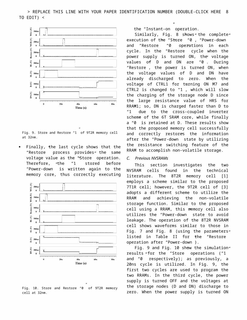
Fig. 16. Layout of the proposed 7T1R NVSRAM. Fig. 18. Layout of the 9T2R NVSRAM [3].
> REPLACE THIS LINE WITH YOUR PAPER IDENTIFICATION NUMBER (DOUBLE-CLICK HERE TO EDIT) <
the proposed cell has excellent performance for non-volatile memory operation and related metrics, as based on the previously presented simulation results.
VI. ADDITIONAL METRICS
In this section, additional metrics as related to area, SNM, process variability and multi-context operation are evaluated and compared among the NVSRAM cells.
A. AreaThe layout of the 8T2R [1], 9T2R [3] and the proposed
7T1R cells are obtained using Cadence Virtuoso [18] at a 32nm MOSFET feature size. As RRAM1 is placed on a different layer [17] than the MOSFETs (using stacking), its area is not included in this evaluation (this condition is applicable to all NVSRAMs considered in this manuscript). Compared with a volatile CMOS (6T) SRAM with an area of 1092λ2 [19], the 8T2R has an area of approximately 3328λ2
(Fig. 15). Comparatively, the proposed non-volatile memory cell further simplifies the design by using only one programmable RRAM and its layout is presented in Fig. 16, i.e. with a cell area of approximately 2958λ2. The layout of 2x2 array for the proposed non-volatile is also shown in Fig. 17 to further demonstrate the feasibility of this design. The 9T2R cell of [3], requires an equalization transistor, thus having a slight area penalty and resulting in an area of 3384λ2
(Fig. 18). Hence also under this metric, the proposed memory cell offers a significant advantage for saving area.
B. Static Noise MarginThe Static Noise Margin (SNM) is considered a metric
for the stability and robustness of a memory cell. The SNM is defined based on the voltage transfer characteristics (VTC) of the complementary storage nodes to characterize the tolerance to noise.
Consider the proposed cell (Fig. 4); the 1T1R RRAM is only turned ON and connected to the 6T SRAM core during the “Store” and “Restore” operations. The transistor M7 turns OFF RRAM1 during the “Read” operation; hence, its effect on the Read SNM (RSNM) can be neglected. Therefore, simulation has concentrated on the Write SNM (WSNM) to evaluate the stability of the proposed cell. Fig. 19 and Fig. 20 show the results at 32nm (using the parameters listed in Table II) for the “Store” “1” and “Store” “0” operations of the proposed NVSRAM cell.
The WSNM is measured using the butterfly plot, obtained from DC simulation by sweeping the input of the inverters (DN and D). For a successful “Store”, only one crosspoint must be found on the butterfly plot, indicating that the cell is monostable; the WSNM for writing a “1” is the width of the smallest square that can be embedded between the lower-right half of the curves (the WSNM for writing a
8
Fig. 15. Layout of the 8T2R NVSRAM [1].. Fig. 17. Layout of 2x2 array using the proposed 7T1R NVSRAM as cell.

Fig. 19. Write Static Noise Margin (WSNM) of 7T1R memory cell for Store “1” at 32 nm.
Fig. 20. Write Static Noise Margin (WSNM) of 7T1R memory cell for Store “0” at 32 nm.
> REPLACE THIS LINE WITH YOUR PAPER IDENTIFICATION NUMBER (DOUBLE-CLICK HERE TO EDIT) <
“0” can be obtained in a similar fashion). The WSNM is the least value between the “Store” “0” and “1” margins; a cell with a low WSNM has a poor “Store” ability. The measured widths of the smallest embedded square of the lower-right half side of Fig. 19 and Fig. 20 are 0.313V and 0.297V, respectively. They are less than the SNM of a 6T SRAM cell, i.e. 0.390V [20]. Using the same method, the WSNMs of the 8T2R and the 9T2R memory cells are given by 0.322V and 0.332V, respectively. These two cells have a better SNM than the proposed cell due to the complementary arrangement used in the NVSRAM cells. Although the addition of a RRAM deteriorates the WSNM of the memory cell, its influence can be mitigated by varying the HRS of RRAM1 (Fig. 21). The increase of the HRS resistance results in an increase in the WSNM up to nearly the value of the 6T SRAM when the HRS value is 30M Ohms. A different core configuration (such as 8T or 9T) can also be used to improve the WSNM.
C. Process VariabilityProcess variability for both the RRAM and the
MOSFET is evaluated for the 7T1R, 8T2R and 9T2R cells using Monte Carlo simulation. As these three cells utilize the same memory core (i.e. a 6T SRAM cell) and the same “Read” operation, only the variability for the “Store” and “Restore” operations is analyzed with respect to the MOSFET threshold voltage (VT) under different technology nodes [12]. As previously, a Gaussian distribution is assumed used and characterized by its mean value (µ) and
the standard deviation (σ) from that mean, i.e. using the 3σ/µ ratio expressed in percentage.
1) RRAM The variability for the RRAM of the non-volatile
SRAM cells is firstly taken into account to characterize its impact; variations in the resistance and threshold voltage of SET/RESET process are evaluated. Consider the proposed operation sequence; the RESET for the RRAM is only used for the “Reset” state of the cells, so the variability of the SET voltage (VS) is pronounced for the “Store” ‘1’ operation when the RRAM is programmed. The standard deviations (σ) of the resistance and VS of the RRAM are set to 10% [21] with respect to mean values of 1KΩ, 1MΩ and 0.5V for LRS, HRS and VS, respectively.
Table V shows the process variability of LRS and HRS for the “Store” and “Restore” operations (a bold entry identifies the least value). Although the proposed 7T1R non-volatile SRAM cell has excellent performance, it has the largest variability percentage values (albeit still very small) among the three memory cells, except for the “Store” ‘1’ in LRS. This is caused by its asymmetrical architecture and leads to the highest variability when the operation of “Restore” ‘0’ is executed. Moreover, the differential scheme of the 8T2R cell [1] shows a lower impact to process variability for the RRAM resistance; however, the 9T2R cell of [3] has the overall least variability percentage values (as shown by the bold entries in Table V). It should be noted that all three NVSRAM
9
Fig. 21. Write Static Noise Margin (WSNM) of 7T1R memory cell versus HRS resistance at 32 nm.
TABLE VVARIABILITY (IN PERCENTAGE) FOR THE THREE NON-VOLATILE SRAM
CELLS AT 32NM
3σ/µ (%)
Parameter 7T1R
8T2R
9T2R
RRAMLRS Store 1 0.209 0.917 0.118
Restore 1 0.578 0.059 0.036HRS Store 0 0.635 0.459 0.257
Restore 0 3.392 0.126 0.075VS Store 1 0.793 0.656 0.237MOSFETVT Store 1 0.422 0.461 0.037
Restore 1 0.572 0.371 0.011Store 0 0.895 0.417 0.184Restore 0 3.003 0.427 0.054

Fig. 22. Timing diagram of 7T1R memory cell for Restore “0” at 32 nm.
> REPLACE THIS LINE WITH YOUR PAPER IDENTIFICATION NUMBER (DOUBLE-CLICK HERE TO EDIT) <
cells have extremely low RRAM variability (i.e. the variability values for the operations of almost all cells are below 1%), hence ultimately a variation in the RRAM has an extremely modest effect on the operation of the NVSRAMs.
2) MOSFETThe simulation results are presented in Table V by
utilizing the parameters under the assumed standard deviation for the threshold voltage (VT) of [12]. These results show that the proposed 7T1R cell also has the largest percentage of variability among the three memory cells, especially for the “Restore” 0 operation. However, its value is only 3% (in most cases the other values are below 1%), so again not as critical to significantly affect the correct operation of the cell.
D. “Restore” OperationThe “Restore” operation for the proposed 7T1R cell is
further assessed with respect to its correct execution and the following additional features.1) Node Capacitance
Compared to the 8T2R cell [1], the proposed 7T1R cell reduces the circuit complexity by utilizing only a RRAM (i.e. a 1T1R) within an asymmetric scheme, but leading to a change in capacitance at the internal nodes D and DN. Using the parameters in Table II, the values of the storage node capacitances in the 7T1R and 8T2R cells (i.e. the internal nodes D and DN) are function of the MOSFET feature size; Table VI shows the values during the “Power-down” ahead of the “Restore” operation. While the 8T2R cell has an equal capacitance at both of these nodes, the asymmetric nature of the proposed 7T1R cell results in different capacitance values at D and DN. As this difference in capacitance value is at most 5% (at 16nm), the large value of the resistance of the connected RRAM (up to 1MΩ) dominates the RC constant as timing for the charging process of the storage node D. Hence the change in node capacitance does not significantly affect the correct execution of the “Restore” operation; it should be noted that if a resistive element with low resistance values (such as for example a memristor) is utilized in the RRAM, then the operations of an asymmetric scheme could be affected. 2) Power Supply and Control Signals
An analysis is pursued for the power supply and the control signals (CTRL1 and CTRL2) to further analyze the correct execution of the “Restore” operation (in particular
for the “Restore” “0”). As discussed previously, the proposed 7T1R cell utilizes the large resistance of the resistive element in the RRAM and the capacitance of the storage node to ensure a correct charging process for node D in the “Restore” “0” operation. It is therefore important to establish the timing relationship between the application of the power and the two control signals (i.e. CTRL2 and CTRL1).
For example if the power supply signal is provided ahead of the control signals, an undefined state could be reached. In addition, if the supply signal is provided long after the control signals, the “Restore” operation could result in incorrect data to the storage node, because M7 is turned on with an initial charge at node D. A detailed timing assessment of “Restore” “0” is therefore pursued. Fig. 22 shows the two values (denoted by tVdd and tCtrl1) of the timing differences between CTRL1 and the supply signal and CTRL2 and CTRL1, respectively. Simulation has shown that tVdd should be no more than 156.2 ps to avoid a long time charge at storage node D, while tCtrl1
should be at least 39.5 ps for a correct “Restore” operation. These values are not very stringent; as shown in Table IV at 32nm, the “Read” and “Store” delays are just above 30 ps, hence tVdd and tCtrl1 are in a time scale greater than the operational delay of the cell.
E. Multi-context ConfigurabilityIn this section, the proposed non-volatile SRAM cell is
assessed with respect to the capability to store and operate under multiple sets of configuration data, as required for FPGA operation [3]. This is referred to as multi-context configurability (MCC). MCC is achieved by connecting parallel 1T1R RRAMs to the same storage node D of a memory cell (Fig. 23). The two signals CTRL1 and CTRL2 of a single memory cell are now given by the multiple-bit signals Control Line (CLi) and Source Line (SLi) for controlling the operation of the ith RRAM cell.
10
TABLE VINODE CAPACITANCE OF 7T1R AND 8T2R CELLS
Feature Size Node Capacitance (aF)7T1R 8T2R
45 nm D 769.3 769.3DN 742.4 769.3
32 nm D 502.7 502.7DN 483.0 502.7
22 nm D 318.3 318.3DN 302.4 318.3
16 nm D 215.3 215.3DN 201.7 215.3

> REPLACE THIS LINE WITH YOUR PAPER IDENTIFICATION NUMBER (DOUBLE-CLICK HERE TO EDIT) <
Simulation has then been performed to find the largest number of parallel RRAM circuits (denoted by k) for correct operation of the MCC in Fig. 23. Except for “Power-down”, the other three operations (“Read”, “Store” and “Restore”) deteriorate by increasing the number of parallel RRAMs. Compared to the other two operations, “Restore” is more affected, because data for “Restore” depends only on each programmed RRAM and its associated CL (a BL is capable of driving a large number of cells). Therefore, evaluation of MCC has been pursued with respect to the four scenarios shown in Table VII. A value of k=42 has been found for the first scenario i.e. when 43 1T1R RRAMs are connected, the storage node D cannot be written back with a “0”. This is mainly due to the signals used for “Restore”, in which CL1 and SL1 are both “1” (while all other signals are “0”). This leads to an erroneous operation when the “Power-on” operation causes a large positive current at node D, thus flipping the expected restored data. The other three scenarios are capable of restoring the data back to the 6T memory cell and a value of k=50 have been found. The above results demonstrate the capability of the proposed NVSRAM cell to be very effective under MCC.
VII. CONCLUSION
This paper has presented a novel design of a non-volatile SRAM (NVSRAM) memory cell that can be used for “Instant-on” operation, i.e. a non-volatile “Restore” signal is utilized to clear the volatile data held in the SRAM and replace it with the data held in the non-volatile storage when a “Restore” operation on “Power-up” is performed. The proposed NVSRAM cell utilizes a 6T SRAM core and a resistive RAM (made of a MOSFET and an Oxide Resistive element). Hence, the proposed cell is a 7T1R cell.
The proposed 7T1R memory cell achieves a significant reduction in energy for its operations required for “Instant-on” operation when compared with other NVSRAM cells found in the technical literature [1, 3 18]. The asymmetric design of the proposed cell however requires more energy when the data is written during normal operation; however its non-volatile nature saves significant energy dissipation, compared to “Standby” of a 6T SRAM cell (as caused mostly by leakage). Furthermore, significant savings in area and the number of MOSFETs have been accomplished. Although the variability in process and resistance is slightly increased for the 7T1R
cell, it is unlikely to have any significant effect on the correct operation of the proposed NVSRAM. Finally, this paper has also shown that the proposed NVSRAM cell offers a significant capability to implement multiple-context configurability, as capable of storing and operating under multiple sets of configuration data for FPGA operation.
REFERENCES
[1] O. Turkyilmaz et al., “RRAM-based FPGA for “Normally Off, Instantly On” Applications,” Proceedings of 2012 IEEE/ACM International Symposium on Nanoscale Architectures, pp. 101-108, 2012.
[2] J. G. Lee, D. H. Kim et al., “A compact HSPICE macromodel of resistive RAM,” IEICE Electronics Express, vol. 4, No. 19, pp. 600-605, 2007.
[3] X. Y. Xue, W. X. Jian et al., “Novel RRAM Programming Technology for Instant-on and High-security FPGAs,” 2011 IEEE 9th International Conference on ASIC (ASICON), pp. 291-294, 2011.
[4] C. E. Herdt, “Nonvolatile SRAM – the Next Generation”, Nonvolatile Memory Technology Review 1993, pp. 28-31, 1993.
[5] H. Akinaga, H. Shima, “Resistive Random Access Memory (ReRAM) Based on Metal Oxides,” Proceedings of the IEEE, pp. 2237-2251, 2010.
[6] T. Miwa, J. Yamada, H. Koike et al., “NV-SRAM: A Nonvolatile SRAM with Backup Ferroelectric Capacitors”, IEEE Journal of Solid-State Circuits, Vol. 36, No. 3, 2001.
[7] M. Takata, K. Nakayama, T. Izumi et al., “Nonvolatile SRAM based on Phase Change”, IEEE Non-Volatile Semiconductor Memory Workshop (NVSMW) 2006, pp. 95-96, 2006.
[8] S. Yamamoto, Y. Shuto, S. Sugahara et al., “Nonvolatile SRAM (NV-SRAM) Using Functional MOSFET Merged with Resistive Switching Devices”, IEEE 2009 Custom Integrated Circuits Conference (CICC), pp. 531-534, 2009.
[9] S. Rajwade, W. K. Yu, S. Xu et al., “Low Power Nonvolatile SRAM Circuit with integrated low power voltage nanocrystal PMOS flash”, 2010 IEEE International SOC Conference (SOCC), pp. 461-466, 2010.
[10] Y. Shuto, S. Yamamoto, S. Sugahara, “Analysis of static noise margin and power-gating efficiency of a new nonvolatile SRAM cell using pseudo-spin-MOSFETs”, IEEE 2012 Silicon Nanoelectronics Workshop (SNW), pp. 1-2, 2012.
[11] M. F. Chang, C. H. Chuang, M. P. Chen et al., “Endurance-Aware Circuit Designs of Nonvolatile Logic and Nonvolatile SRAM Using Resistive Memory (Memristor) Device”, 2012 17th Asia and South Pacific Design Automation Conference (ASP-DAC), pp. 329-334, 2012.
[12] A. Rubio, J. Figueras, E. I. Vatajelu et al., “Process variability in sub-16nm bulk CMOS technology,” Online. Available: http://hdl.handle.neu/2117/15667, 2012.
[13] P. F. Chiu, M. F. Chang, S. S. Sheu, et al., “A low store energy, low VDDmin, nonvolatile 8T2R SRAM with 3D stacked RRAM devices for low power mobile applications,” 2010 Symposium on VLSI Circuits (VLSIC), pp. 229-230, 2010.
[14] A. Chen, S. Haddad, Y. C. Wu et al., “Erasing characteristics of Cu 2O metal-insulator-metal resistive switching memory,” Appl. Phys. Lett., vol. 92, pp. 013503-1-013503-3, 2008.
[15] S. Onkaraiah, J. M. Portal, “Using OxRRAM Memories for Improving Communications of Reconfigurable FPGA Architectures,” Proceedings of 2011 IEEE.ACM International Symposium on Nanoscale Architecture, pp. 65-69, 2011.
11
TABLE VIISIMULATED MCC SCENARIOS FOR PROPOSED 7T1R MEMORY CELL
Memory Cell RRAM 1 All remaining k-1 RRAMs
Programmed Stored Data
0 0
0 11 01 1
Fig. 23. Multiple-context configuration of proposed 7T1R cell.

> REPLACE THIS LINE WITH YOUR PAPER IDENTIFICATION NUMBER (DOUBLE-CLICK HERE TO EDIT) <
[16] D. Lee et al., "Resistance switching of copper doped MoOx films for nonvolatile memory applications", Appl. Phys. Lett. 90, 122104 (2007).
[17] B. Govoreanu, G.S. Kar, Y. Y. Chen, et al., “10x10nm2 Hf/HfOx
Crossbar Resistive RAM with excellent performance, reliability and low-energy operation,” 2011 IEEE International Electron Devices Meeting (IEDM), pp. 31.6.1-31.6.4, 2011.
[18] “Cadence Virtuoso,” www.cadence.com.[19] J. M. Rabaey, A. Chandrakasan and B. Nikolic, “Digital Integrated
Circuits: A Design Perspective (Second Edition)”, Prentice Hall, pp. 665, ISBN: 0130909963, 2003.
[20] J. Wang, S. Nalam, and B. H. Calhoun, “Analyzing Static and Dynamic Write Margin for Nanometer SRAMs”, Proc. 2008 ACM/IEEE International Symposium on Low Power Electronics and Design (ISLPED), pp. 129-134, Aug 2008.
[21] IEEE IEDM, Presentation, Short Course on Emerging Memories, 2011.
Wei Wei (S’13) received the B.S. degree in applied physics from Beihang University, Beijing, China, in 2009, and the M.S. degree in electrical and computer engineering from Northeastern University, Boston, in 2011. He is currently working towards the Ph.D. degree in computer engineering at Northeastern University, Boston, MA.
From 2009 to present, he was involved in low-power and high performance integrated circuit design and test. His research interests include low-
power VLSI design, PVT design techniques for robust nanoscale CMOS circuits, novel memory physical design and methodologies and nanoscale digital device modeling.
Kazuteru Namba (M’04) received B.E., M.E. and Ph.D. from Tokyo Institute of Technology in 1997, 1999 and 2002, respectively. He joined Chiba University in 2002. He is currently an Assistant Professor of Graduate School of Advanced Integration Science, Chiba University. His current research interests include dependable computing. He is a member of the IEICE and the IPSJ.
Jie Han (S’02–M’05) received the B.Sc. degree in electronic engineering from Tsinghua University, Beijing, China, in 1999 and the Ph.D. degree from Delft University of Technology, The Netherlands, in 2004. Currently, he is an assistant professor in the Department of Electrical and Computer Engineering at the University of Alberta, Edmonton, AB, Canada.
His research interests include reliability and fault tolerance, nanoelectronic circuits and systems, and novel computational models for nanoscale and biological applications. Dr. Han is
serving as a Guest Editor for the Special Issue of “Approximate and Stochastic Computing” in IEEE Transactions on Emerging Topics in Computing (TETC). He served as a General Chair and Technical Program
Chair in IEEE International Symposium on Defect and Fault Tolerance in VLSI and Nanotechnology Systems (DFT), 2013 and 2012, respectively. He also served as a Technical Program Committee Member in several other international symposia and conferences..
Fabrizio Lombardi (M’81–SM’02-F’09) graduated in 1977 from the University of Essex (UK) with a B.Sc. (Hons.) in Electronic Engineering. In 1977 he joined the Microwave Research Unit at University College London, where he received the Master in Microwaves and Modern Optics (1978), the Diploma in Microwave Engineering (1978) and the Ph.D. from the University of London (1982).
He is currently the holder of the International Test Conference (ITC) Endowed Chair Professorship at Northeastern University, Boston.
His research interests are bio-inspired and nano manufacturing/computing, VLSI design, testing, and fault/defect tolerance of digital systems. He has extensively published in these areas and coauthored/edited seven books.
12