joseph anthony prathap & t.s. anandhi · fig. 3: design flow for the modified dpi enabled...
TRANSCRIPT

© 2017. Joseph Anthony Prathap & T.S. Anandhi. This is a research/review paper, distributed under the terms of the Creative Commons Attribution-Noncommercial 3.0 Unported License http://creativecom mons.org/ licenses/by-nc/3.0/), permitting all non commercial use, distribution, and reproduction in any medium, provided the original work is properly cited.
Global Journal of Researches in Engineering: F Electrical and Electronics Engineering Volume 17 Issue 1 Version 1.0 Year 2017 Type: Double Blind Peer Reviewed International Research Journal Publisher: Global Journals Inc. (USA)
Online ISSN: 2249-4596 & Print ISSN: 0975-5861
FPGA Based Hybrid Digital PWM for DC-DC Voltage Regulator
Joseph Anthony Prathap & T.S. Anandhi Annamalai University
Abstract- This In general, telecommunication applications require low voltage, high current and reduced size power supplies. Selection of high switching frequency helps in the reduction of the DC-DC converter size. In this work, Digital PI (DPI) enables the Digital Pulse Width Modulation (DPWM) generator for generating high switching frequencies are developed and implemented using VHDL coding and Xilinx Spartan 3A DSP Field Programmable Gate Array (FPGA) kit. Hardware result of voltage regulation depicts the superiority and robustness of the proposed DPI enabled DPWM (MD-DPWM) methods under line and load disturbances. The MD-DPWM technique can be used to generate a very high switching frequency up to 1 MHz and more. Also the MD-DPWM proves to be cost effective, as it consumes low power and area.
Keywords: digital pulse width modulation, digital proportional integral-dc-to-dc buck converter, xilinx spartan 3A DSP field programmable gate array.
GJRE-F Classification: FOR Code: 090607
FPGABasedHybridDigitalPWMforDCDCVoltageRegulator
Strictly as per the compliance and regulations of :

FPGA Based Hybrid Digital PWM for DC-DC Voltage Regulator
Abstract- In general, telecommunication applications require low voltage, high current and reduced size power supplies. Selection of high switching frequency helps in the reduction of the DC-DC converter size. In this work, Digital PI (DPI) enables the Digital Pulse Width Modulation (DPWM) generator for generating high switching frequencies are developed and implemented using VHDL coding and Xilinx Spartan 3A DSP Field Programmable Gate Array (FPGA) kit. Hardware result of voltage regulation depicts the superiority and robustness of the proposed DPI enabled DPWM (MD-DPWM) methods under line and load disturbances. The MD-DPWM technique can be used to generate a very high switching frequency up to 1 MHz and more. Also the MD-DPWM proves to be cost effective, as it consumes low power and area. Keywords: digital pulse width modulation, digital proportional integral-dc-to-dc buck converter, xilinx spartan 3A DSP field programmable gate array.
I. Introduction
uck converter is a circuit which step downs the voltage and step ups the current. A basic buck converter circuits requires inductor, diode and
transistor as switch. As per the control of the switch by the PWM signals the inductor acts against the input voltage. The DPWM design involves digital circuits like adders, flip-flops, multiplexers, counters and shift registers.
DPWM has advantages like easy design, high accuracy, low area and low power consumption. High resolution digitally controlled DC-DC buck converter is designed without the use of high frequency clock [1]. FPGA based implementation of the DPWM is very simple comparatively consuming of few memories, multipliers and adders [2]. DPWM architecture developed with FPGA implies high reliability, linearity and low latency [3]. A brushless DC machines can be digitally controlled by FPGA implementation with no additional hardware and hence has low design complexity [4].
A DPWM technique in [5] gives consistent off-time and on-time control under heavy load and light load conditions with reduced switching losses. FPGA based high resolution DPWM designed using a digital clock manager and I/O delay elements have low cost and higher clock frequency [6]. In this work, the performances of the DC-DC buck converter with the DPWM as voltage regulator is analyzed.
II. Dc-Dc Buck Converter
The closed loop DC-DC buck converter with the proposed DPI enables the DPWM technique is shown in the Fig.1.
DC-DC Buck Converter
Analog to DigitalConverter
AD7266
Modified DPIenabled Hybrid
DPWMController
FEE
D B
AC
K (fb V
alue )
fb Value
DC INPUT
DPWMCONTROL
DCREGULATED
OUTPUT
FPGA IMPLEMENTATION
2N bit
Fig.1: Closed loop DC-DC Buck Converter with MD-DPWM control
B
Globa
l J o
urna
l of
Resea
rche
s in E
nginee
ring
(
)Volum
e X
VII
Issu
e I
Version
I
7
Year
2017
F
© 2017 Global Journals Inc. (US)
Joseph Anthony Prathap α & T.S. Anandhi σ
Author α: Research Scholar, Department of Electronics and Instrumentation Engineering, Annamalai University, Chidambaram, India. e-mail: [email protected] σ: Associate Professor, Department of Electronics and Instrumentation Engineering, Annamalai University, Chidambaram, India. e-mail: [email protected]

The output voltage of the buck converter is less than the input voltage and is controlled by the duty cycle “d”. The duty cycle “d” is the ratio of the ON period to the total period cycle of the controlling square pulse.
d = TonT
Where “Ton”refers to the ON period. “T” refers to the total time period of the cycle.
The operation of the buck converter is related to the duty cycle as given below
Vout = d. Vin
Where “d” is the duty cycle. “Vin” is the input voltage of the buck converter.“Vout” is output voltage of the buck converter.
The digital switching control has more advantages like easy designing, high manipulation power, upgradable, immune to environmental changes, easy debugging.
In our work, the FPGA based DPWM DC-DC buck voltage regulator, is implemented which satisfies the demand of low voltage and high current application. ADC is utilized for the purpose of acquiring the feedback values of the DC-DC buck converter into the FPGA. ADC IC AD7266 has Successive Approximation Circuit (SAC) and is used for real time implementation. The FPGA based ADC architecture helps in the evaluation of digital error with high accuracy [7]. The Digital PI (DPI) control algorithm is designed using VHDL coding enables the DPWM. The Modified DPI enabled DPWM (MD-DPWM) generators are implemented by FPGA and found to perform efficiently for the disturbances and component variation. The AD7266 is provided to access the analog value in the form of digital equivalence (2N).
III. Digital Pulse Width Modulation Methods
The Digital Pulse Width Modulated (DPWM) signal is generated using logical design. The DPWM is generated by three methods. They arei) Counter DPWM method. (CDPWM)ii) Delay line DPWM method. (DDPWM)iii) Hybrid DPWM method. (HDPWM)
Using ModelSim, the three DPWM methods are simulated. From the simulated results, the HDPWM generator is found to be advantages when compared to the CDPWM and DDPWM. The CDPWM require high frequency system clock and thus has high power consumption. The DDPWM occupies more area increasing the cost. The relationship of the clock frequency and the switching frequency for the DPWM generator is
FCLK = FSW x 2nFSW-Switching frequency
FCLK -Clock frequency 2n- Resolution in bits
In this work, the design of the Modified DPI enabled DPWM using 211-bit resolution is used which yields FSW of 12.5 KHz and achieved the FCLK of 21 MHz Hybrid DPWM generator is the combination of both counter based DPWM and delay-line based DPWM methods. The DC input signal of 211-bit resolution is bit split into 25-bit and 26-bit resolutions. In which 25-bitresolution is used for the generation of the DDPWM and 26-bit resolution for the generation of the CDPWM generation. The HDPWM has two set of SET and RESET signal (each from CDPWM and DDPWM generations) which are logically ANDed to give a SET and RESET signal for the SR-flip-flop are shown in Fig.2.
Fig. 2: SIMULINK-MATLAB block of Hybrid based DPWM
IV. THE PROPOSED METHOD: MODIFIED DPIENABLED DPWM GENERATOR
The modified DPWM generator utilizes the DPI controller to manipulate the duty cycle proportionate to the error as well as enable the DPWM generator. Real time feedback equivalence value of 0 to 5V is selected by the VHDL coding and fed to the ADC for processing.
gain parameters are kp=0.6 and ki=0.055. The DPI controller values are made visible by interfacing the 12 LEDs of the FPGA. The increase and decrease push buttons available in the FPGA kit is also activated for varying the voltage reference value. These push switch values are coded along with the limiter. These values are interfaced with the LCD display of the FPGA in order to monitor the variable set values and the settling values.Initially the set value is maintained at 10V by default in
FPGA Based Hybrid Digital PWM for DC-DC Voltage Regulator
© 2017 Global Journals Inc. (US)
Gl oba
l Jo
urna
l of
Resea
rche
s in E
nginee
ring
(
)Volum
e X
VII
Issu
e I
Version
I
8
Year
2017
F
The resolution for the ADC is 211 bits. The DPI controller

the VHDL code. The structural style of VHDL code is used in the design of MD-DPWM
Bit splitter
25 bit CDPWM technique 25 bit DDPWM technique
AND gate AND gate
SR-Flip Flop
DC-DC Buck Converter kit
ADC (IC AD7266) of Xilinx Spartan 3ADSP FPGA
DPI Controller (VHDL Code)
210 bit equivalent converter
SET RESET
RESET1SET1 RESET2SET2
Signal Conditioning Circuit (SCC)
DC control signal
0 to 5V
210
2525
Reference Value
0 to 20V
Feedback Value
Duty cycle
Fig. 3: Design flow for the Modified DPI enabled Hybrid DPWM controlled DC-DC buck converter using FPGA
The VHDL code uses mixed style of modeling. The FPGA implementation of the Modified DPI enabled Hybrid DPWM generator (MD-HDPWM) demands more real-time considerations like selection of resolution, uniformity of resolution, accurate digital equivalence for the obtained analog value, digitized comparison of AV and SP, and stabilizing the MD-DPWM control. The desired set point/ voltage reference (SP), kp and ki are fixed within the VHDL code. All these values are converted to bits. The actual value (AV) is measured as bit equivalents by the use of ADC AD7266. The values of the SP and AV are compared to evaluate the errors. Fig.3 shows the flowchart for the VHDL coded Modified DPI enabled DPWM controller.
Resolution refers to the number of bits used in the design. In this work, the three MD-DPWM generators are designed using 211 bit resolution. The MD-CDPWM generator uses a 211 bit (2047 count) counter. The MD-DDPWM generator uses the 2048:1 multiplexer. The MD-HDPWM generator uses 211 bit resolution in which 25 bit is used for the MD-DDPWM generation part and 26
bit is used for the MD-CDPWM generation part. The frequency of the DPWM generator is 12.5 KHz in the hardware due to the limitations in frequency range with
the laboratory prototype. To achieve this frequency, the VHDL coding utilizes the scaled value given by the formula.
Scaled_value =1
2n X Output frequency X Clock period
Where Clock period is 100 nsOutput frequency is 12.5 KHz
V. HARDWARE DETAILS
The Xilinx Spartan 3A DSP FPGA is used for the design of the DC-DC buck type voltage regulator using MD-HDPWM. The Xilinx Spartan 3A DSP has IC AD7266 for the design of ADC. The set point variations are provided by the two variable push switches. The 16*4 LCD display is activated by the VHDL code. The VHDL codes for the DPI and ADC are designed with 10 times of the actual values to accomplish the FPGA requirements. This scaling is done to make sure that the fractional changes of the ADC and DPI are considered in the design, as the Xilinx Spartan 3A DSP kit do not support the float value implementation.
The AD7266 is 8 channels SAR ADC with
IC which operates from 2.7V to 5.25V of supply. The
FPGA Based Hybrid Digital PWM for DC-DC Voltage Regulator
Globa
l J o
urna
l of
Resea
rche
s in E
nginee
ring
(
)Volum
e X
VII
Issu
e I
Version
I
9
Year
2017
F
© 2017 Global Journals Inc. (US)
a) Resolution
maximum resolution of 212 bits. The AD7266 is a 32 pin
ADC performs two functions of sampling and conversion of two channels simultaneously. These conversion values are concurrently accessible in separate data lines. When operated at 3V, the AD7266 gives a throughput rate of 1.5 MSPS with maximum power dissipation of 11.4 mW. Thus low power consumption for high throughput is achieved. The AD7266 has zero pipeline delay; since the sampling control of the two SAR ADCs are accurate. The ADC has two input ranges like 0V to VREF and 2*VREF
VI. RESULTS AND DISCUSSIONS
the set-point change and Fig.13 shows experimental DSO output for the positive and negative line disturbances.
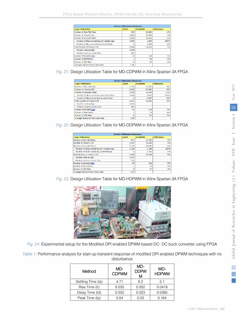
Fig.14&15 indicate the performance of the MD-HDPWM based DC-DC buck converter in closed loop with load disturbances from 445Ω to 595Ω and 595Ω to 445Ω respectively. The set point is 10 V and input voltage is 20V. The settling time measured during the negative load disturbance with MD-HDPWM seems to be very minimal. Fig.16&17 show the experimental DSO response of load disturbance from 445 Ω to 595Ω and from 595Ω to 445Ω respectively for the MD-HDPWM in closed loop. Fig.18 shows experimental output response when the load is changed from 470 Ω to 495Ω and from 495Ω to 470Ω using MD-DDPWM. Fig.19 shows experimental output for the negative load disturbance from 445Ω to 295Ω using MD-DDPWM. The RTL schematic for the MD-HDPWM technique is presented in Fig.20. Fig.21,22,&23 show the design utilization chart for the MD-CDPWM, MD-DDPWM and MD-HDPWM respectively. The experimental setup of DC-DC buck converter using the Xilinx Spartan 3A DSP is shown in Fig.24.
VII. COMPARISON AND ANALYSIS
Table I shows that the Modified DPI enabled HDPWM has lower steady state error and low settling time for the step change variation. The peak overshoot percentage is also less in MD-HDPWM. Table I also show that MD-HDPWM used with the closed loopDC-DC buck converter has less settling time and rise time when compared to the other two like MD-CDPWM and MD-DDPWM methods. Table II & III show the settling time for both the positive and negative line disturbances are good for the MD-HDPWM. Table IV shows that the MD-HDPWM has lower area utilization in FPGA device compared to the MD-DPWM and also the clock frequency of the MD-HDPWM is less in comparison of the MD-CDPWM. Thus the modified DPI enabled HDPWM method is cost effective in comparison with the other methods.
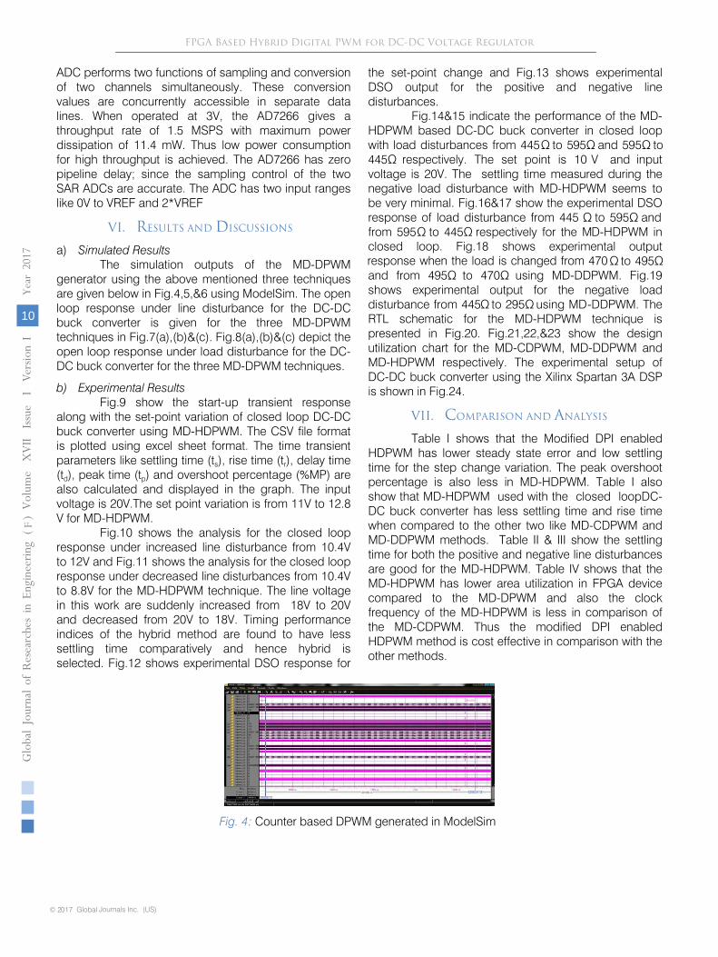
Fig. 4: Counter based DPWM generated in ModelSim
FPGA Based Hybrid Digital PWM for DC-DC Voltage Regulator
© 2017 Global Journals Inc. (US)
Gl oba
l Jo
urna
l of
Resea
rche
s in E
nginee
ring
(
)Volum
e X
VII
Issu
e I
Version
I
10
Year
2017
F
a) Simulated Results
b) Experimental Results
The simulation outputs of the MD-DPWM generator using the above mentioned three techniques are given below in Fig.4,5,&6 using ModelSim. The open loop response under line disturbance for the DC-DC buck converter is given for the three MD-DPWM techniques in Fig.7(a),(b)&(c). Fig.8(a),(b)&(c) depict the open loop response under load disturbance for the DC-DC buck converter for the three MD-DPWM techniques.
Fig.9 show the start-up transient response along with the set-point variation of closed loop DC-DC buck converter using MD-HDPWM. The CSV file format is plotted using excel sheet format. The time transient parameters like settling time (ts), rise time (tr), delay time (td), peak time (tp) and overshoot percentage (%MP) are also calculated and displayed in the graph. The input voltage is 20V.The set point variation is from 11V to 12.8 V for MD-HDPWM.
Fig.10 shows the analysis for the closed loop response under increased line disturbance from 10.4V to 12V and Fig.11 shows the analysis for the closed loop response under decreased line disturbances from 10.4V to 8.8V for the MD-HDPWM technique. The line voltage in this work are suddenly increased from 18V to 20V and decreased from 20V to 18V. Timing performance indices of the hybrid method are found to have less settling time comparatively and hence hybrid is selected. Fig.12 shows experimental DSO response for

FPGA Based Hybrid Digital PWM for DC-DC Voltage Regulator
Globa
l J o
urna
l of
Resea
rche
s in E
nginee
ring
(
)Volum
e X
VII
Issu
e I
Version
I
11
Year
2017
F
© 2017 Global Journals Inc. (US)
Fig. 5: Delay line based DPWM generated in ModelSim
Fig. 6: Hybrid based DPWM generated in ModelSim
(a)
(b)
(c)
Fig. 7: Open loop deviated response of DC-DC buck converter with line disturbance using a) MD-CDPWM. b) MD-DDPWM. c) MD-HDPWM

FPGA Based Hybrid Digital PWM for DC-DC Voltage Regulator
© 2017 Global Journals Inc. (US)
Gl oba
l Jo
urna
l of
Resea
rche
s in E
nginee
ring
(
)Volum
e X
VII
Issu
e I
Version
I
12
Year
2017
F
(a)
(b)
(c)
Fig. 8: Open loop deviated response of DC-DC buck converter with load disturbance using a) MD-CDPWM. b) MD-DDPWM. c) MD-HDPWM
Fig. 9: Experimental regulated start-up transient response of MD-HDPWM buck converter with set point variation
Fig. 10: Experimental response of MD-HDPWM based DC-DC buck converter with increased load disturbance from 10.4V to 12V

FPGA Based Hybrid Digital PWM for DC-DC Voltage Regulator
Globa
l J o
urna
l of
Resea
rche
s in E
nginee
ring
(
)Volum
e X
VII
Issu
e I
Version
I
13
Year
2017
F
© 2017 Global Journals Inc. (US)
Fig. 11: Experimental response of MD-HDPWM based DC-DC buck Converter with decreased load disturbance from 10.4V to 8.8V
Fig .12: Experimental DSO start-up transient response of MD-HDPWM buck type voltage regulator with set point variation
Fig. 13: Experimental DSO regulated response of MD-HDPWM buck type voltage regulator with line disturbances from 10.4V to 8.8V and 10.4V to 12V
Fig. 14: Experimental CSV plotted result for Load disturbance of MD-HDPWM buck type voltage regulator from 445Ω to 595Ω
Fig. 15: Experimental CSV plotted result for Load disturbance for MD-HDPWM buck type voltage regulator from 595Ω to 445Ω

FPGA Based Hybrid Digital PWM for DC-DC Voltage Regulator
© 2017 Global Journals Inc. (US)
Gl oba
l Jo
urna
l of
Resea
rche
s in E
nginee
ring
(
)Volum
e X
VII
Issu
e I
Version
I
14
Year
2017
F
Fig. 16: Experimental DSO result for Load disturbance for MD-HDPWM buck type voltage regulator from 445Ω to 595Ω
Fig. 17: Experimental DSO response for Load disturbance for MD-HDPWM buck type voltage regulator from 595Ω to445Ω
Fig. 18: Experimental DSO response for Load disturbance for MD-DDPWM buck type voltage regulator from 470Ω to 495Ω and from 495Ω to 470Ω
Fig.19: Experimental DSO response for Load disturbance for MD-DDPWM buck type voltage regulator from 445Ω to 295Ω
Fig. 20: Detailed RTL view of MD-HDPWM in Xilinx ISE
FPGA Based Hybrid Digital PWM for DC-DC Voltage Regulator
Globa
l J o
urna
l of
Resea
rche
s in E
nginee
ring
(
)Volum
e X
VII
Issu
e I
Version
I
15
Year
2017
F
© 2017 Global Journals Inc. (US)
Fig. 21: Design Utilization Table for MD-CDPWM in Xilinx Spartan 3A FPGA
Fig. 22: Design Utilization Table for MD-DDPWM in Xilinx Spartan 3A FPGA
Fig. 23: Design Utilization Table for MD-HDPWM in Xilinx Spartan 3A FPGA
Fig. 24: Experimental setup for the Modified DPI enabled DPWM based DC- DC buck converter using FPGA
Table 1: Performance analysis for start-up transient response of modified DPI enabled DPWM techniques with no disturbance
Method MD-CDPWM
MD-DDPW
M
MD-HDPWM
Settling Time (ts) 4.71 6.2 5.1Rise Time (tr) 0.035 0.002 0.0419
Delay Time (td) 0.032 0.023 0.0385Peak Time (tp) 0.04 0.03 0.164

FPGA Based Hybrid Digital PWM for DC-DC Voltage Regulator
© 2017 Global Journals Inc. (US)
Gl oba
l Jo
urna
l of
Resea
rche
s in E
nginee
ring
(
)Volum
e X
VII
Issu
e I
Version
I
16
Year
2017
F
Steady State Error (ess)
0.0425 0.0385 0.0357
Step change variation time(tsc)
3.6 2.4 1.9
Percentage Overshoot (%MP)
113.04% 96% 78.18%
Table 2: Performance Analysis For Start-Up Transient Response Of Modified DPI Enabled DPWM Techniques With Increased Line Disturbance
Methods MD-CDPWM
MD-DDPWM
MD-HDPWM
Rise Time in s (tr) 0.2 0.3 0.2
Time Delay in s (tp) 0.1 0.1 0.1
Settling Time in s (ts) 3.8 2.7 1.6
Percentage Overshoot(%MP) 14.286% 17.647% 15.38%
Output Voltage Ripple 0.04 0.04 0.03846
Initial Value before disturbance
9.8 V 10.2 V 10.4 V
Peak Value at disturbance 11.2 V 12 V 12 V
Methods MD-CDPWM
MD-DDPWM
MD-HDPWM
Rise Time in s (tr) 0.2 0.2 0.23
Time Delay in s (tp) 0.142 0.135 0.13
Settling Time in s (ts) 3.26 2.82 2.62
Percentage Overshoot (% MP) 14.2857% 13.725% 15.38%
Output Voltage Ripple 0.04 0.04 0.04
Initial Value before disturbance 9.8 V 10.2 V 10.4 V
Minimum Value at disturbance 8.4 V 8.8V 8.8 V
Methods MD-CDPWM
MD-DDPWM
MD-HDPWM
Resolution with specification
211-bit Counter
Designed
211 2048 : 1 Mux
Designed
211=26+25
(26-bitCounter & 32:1 Mux Designed)
Number of Sliced Flip Flops
665 2716 697
Number of 4 input LUTs
1633 2670 1657
Number of occupied slices
1090 3659 1130
Number of bonded IOBs
37 41 37
Average Fan-out of Non-clock
nets2.96 2.59 2.95
Table 3: Performance Analysis For Start-Up Transient Response Of Modified DPI Enabled DPWM Techniques With Decreased Line Disturbance
Table 4: Device Utilization For The Modified DPI Enabled DPWM Techniques

FPGA Based Hybrid Digital PWM for DC-DC Voltage Regulator
Globa
l J o
urna
l of
Resea
rche
s in E
nginee
ring
(
)Volum
e X
VII
Issu
e I
Version
I
17
Year
2017
F
© 2017 Global Journals Inc. (US)
VIII. CONCLUSION
Simulation results show the possibilities of achieving high switching frequency up to 16MHz DPWM. Hardware results show the feasibility of the proposed technique for the available prototype model in our laboratory and found to be satisfactory. The Modified DPI enabled DPWM generators also perform voltage regulation of the power supply. The FPGA based Modified DPI enabled Hybrid based DPWM voltage regulator is found to be immune to circuit component variations, and also to line–load disturbances.
References Références Referencias
1. Luca Corradini, Aleksandar Bjeleti´c, Regan Zane, and Dragan Maksimovi´c, “Fully Digital Hysteretic Modulator for DC–DC Switching Converters” IEEE Transactions on Power Electronics, Vol. 26, No. 10, pp. 2969-2979, October 2011.
2. Bo Li, Xuefang Lin-Shi, Bruno Allard, and Jean-Marie Rétif, “A Digital Dual-State-Variable Predictive Controller for High Switching Frequency Buck Converter With Improved Σ-DPWM” IEEE Transactions on Industrial Informatics, Vol. 8, No. 3, pp. 472-481, August 2012.
3. Daniel Costinett, Miguel Rodriguez, and Dragan Maksimovic, “Simple Digital Pulse Width Modulator under 100 ps Resolution Using General-Purpose FPGAs” IEEE Transactions on Power Electronics, Vol. 28, NO. 10, pp.4466-4472, October 2013.
4. Nikola Milivojevic, Mahesh Krishnamurthy, Yusuf Gurkaynak, Anand Sathyan, Young-Joo Lee, and Ali Emadi, “Stability Analysis of FPGA-Based Control of Brushless DC Motors and Generators Using Digital PWM Technique” IEEE Transactions on Industrial Electronics, Vol. 59, No. 1, pp. 343-351, January 2012.
5. Chia-An Yeh, and Yen-Shin Lai, “Digital Pulse width Modulation Technique for a Synchronous Buck DC/DC Converter to Reduce Switching Frequency” IEEE Transactions on Industrial Electronics, Vol. 59, No. 1, pp. 550-561, January 2012.
6. Denis Navarro, O´ scar Luc´ıa, Luis Angel Barraga´n, Jose´ Ignacio Artigas, Isidro Urriza,n and O´ scar Jime´nez, “Synchronous FPGA-Based High-Resolution Implementations of Digital Pulse-Width Modulators” IEEE Transactions on Power Electronics, Vol. 27, No. 5, pp.2515-2525, May 2012.
7. Mukti Barai, Sabyasachi Sengupta, and Jayanta Biswas, “Digital Controller for DVS-Enabled DC–DC Converter” IEEE Transactions on Power Electronics, Vol. 25, No. 3, pp. 557-573, March 2010.

This page is intentionally left blank
FPGA Based Hybrid Digital PWM for DC-DC Voltage Regulator
© 2017 Global Journals Inc. (US)
Gl oba
l Jo
urna
l of
Resea
rche
s in E
nginee
ring
(
)Volum
e X
VII
Issu
e I
Version
I
18
Year
2017
F