journal of alloys and compounds - gisticserv.gist.ac.kr/mis/publications/data/2016/45... ·...
TRANSCRIPT

lable at ScienceDirect
Journal of Alloys and Compounds 688 (2016) 12e17
Contents lists avai
Journal of Alloys and Compounds
journal homepage: http: / /www.elsevier .com/locate/ ja lcom
Influence of annealing temperature on the properties and solar cellperformance of Cu2SnS3 (CTS) thin film prepared using sputteringmethod
In Young Kim a, Ju Yeon Lee b, Uma V. Ghorpade b, c, M.P. Suryawanshi b, Dong Seon Lee a, *,Jin Hyeok Kim b, **
a School of Electrical Engineering and Computer Science, Gwangju Institute of Science and Technology, 123 Cheomdangwagi-ro, Buk-gu, Gwangju 500-712,South Koreab Optoelectronics Convergence Research Center, Department of Material Science and Engineering, Chonnam National University, 300 Yongbong-Dong, Puk-Gu, Gwangju 500-757, South Koreac Analytical Chemistry and Material Science Research Laboratory, Department of Chemistry, Shivaji University, Kolhapur 416-004, India
a r t i c l e i n f o
Article history:Received 23 February 2016Received in revised form21 June 2016Accepted 26 June 2016Available online 28 June 2016
Keywords:Cu2SnS3SputteringThin film solar cell
* Corresponding author.** Corresponding author.
E-mail addresses: [email protected] (D.S. Le(J.H. Kim).
http://dx.doi.org/10.1016/j.jallcom.2016.06.2640925-8388/© 2016 Elsevier B.V. All rights reserved.
a b s t r a c t
Highly crystallized Cu2SnS3 (CTS) thin films are synthesized by sputtering based deposition route.Further, Influence of different annealing temperatures on crystallographic, electrical and optical prop-erties of CTS thin films have been investigated. The synthesized CTS thin films are grown as a monoclinicstructure observed from X-ray diffraction (XRD) of (112), (220), and (312) plane and it is furtherconfirmed using Raman spectroscopy by the presence of Raman peaks at 295 and 354 cm�1. The directband gap energy of CTS thin film annealed at 580 �C is found to be 1.03 eV by extrapolation from externalquantum efficiency (EQE) measurement. An X-ray photoelectron spectroscopy (XPS) study suggests thatthe ionic states of Cu, Sn, and S are Cuþ,Sn4þ, and S2�, respectively. The CTS based thin film solar cells(TFSCs) are fabricated with a structure of Mo/CTS/CdS/i-ZnO/AZO/Al. The preliminary power conversionefficiency of 1.35% with a short circuit current density of 28.3 mA/cm2, an open circuit voltage of147.5 mV, and a fill factor of 32% were obtained, although the processing parameters have not yet beenoptimized.
© 2016 Elsevier B.V. All rights reserved.
1. Introduction
Recent interest in thin film photovoltaics was primarily moti-vated by the improvements in conversion efficiency of solar cellsbased on various materials, including CdTe, Cu(In, Ga)Se2 (CIGS),and Cu2ZnSnS4 (CZTS) [1e3]. Currently, p-type semiconductorCu2SnS3 (CTS) has received considerable attention as a suitablecandidate for thin film solar cells (TFSCs) and a great deal ofresearch for CTS has also been reported. CTS is a suitable materialfor photovoltaic cells because of its high optical absorption coeffi-cient (~104 cm�1), wide range of band gap energy, and earthabundant materials having the theoretical power conversion
efficiency of 30%; it has the potential to become a commercialabsorber material in TFSCs [4e6]. Compared to the existing qua-ternary chalcogenide based CIGS and CZTS thin films, CTS is able tocontrol the secondary phases that are formed when an absorberlayer is synthesized.
Researchers have reported that the crystal structure of CTS de-pends on the films deposition method and annealing environmentsbecause CTS exhibits a different type of crystal structure that formsa diverse range of band gap energy [4,7]. Moreover, a diverse crystalstructure can be formed and the wide range of band gap energy(0.93e1.77 eV) is able to be controlled by synthesis method [6,8].Using the evaporation method, K. Chino fabricated CTS thin filmsthat have a cubic, monoclinic and/or tetragonal crystal structure,with a band gap energy of 0.96e1.00 eV [9]. H Guan fabricated CTSthin films that show a cubic and tetragonal crystal structure with1.05 and 1.19 eV band gap energy, respectively, by successive ioniclayer adsorption and reaction method [10]. R. Bodeux also reportedCTS thin films with a tetragonal phase with a band gap energy of
20 30 40 50 60 70 80
Inte
nsity
[a.u
.]
2θ [deg.]
CTS-580
CTS-560
CTS-540
MoMoMoCTS-520
Monoclinic CTS
Cubic CTS
Tetragonal CTS
(a)
27.5 28.0 28.5 29.0 29.5
Inte
nsity
[a.u
.]
(b)
28.36 Cubic SnS28.40
28.44
28.54 Tetragonal CTSCubic CTS
Monoclinic CTS
CTS-520
CTS-540
CTS-560
CTS-580
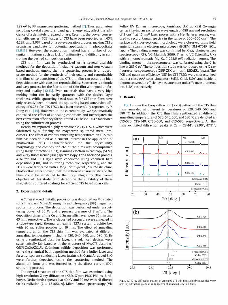
2θ [deg.]Fig. 1. (a) X-ray diffraction pattern of annealed CTS thin films and (b) magnified viewof (112) diffraction plane in XRD spectra of annealed CTS thin films.
I.Y. Kim et al. / Journal of Alloys and Compounds 688 (2016) 12e17 13
1.28 eV by RF magnetron sputtering method [7]. Thus, parametersincluding crystal structure, band gap energy etc., affect the effi-ciency of a definitely prepared phase. Recently, the power conver-sion efficiencies (PCE) values of CTS have been reported as 4.63%,4.29%, and 3.66% based on a co-evaporation process, making CTS apromising candidate for potential applications in photovoltaics[2,6,11]. However, the evaporation method has a number of po-tential limitations such as lack of uniformity and difficulty in con-trolling the desired composition ratio.
CTS thin film can be synthesized using several availablemethods for the deposition, including vacuum and non-vacuumbased methods. Among them, a sputtering process is an appro-priate method for the synthesis of high quality and reproduciblethin films since deposition of the CTS thin film can occur at a highdeposition ratewith constant reproducibility. Sputtering is a simpleand easy process for the fabrication of thin film with good unifor-mity and quality [12,13]. Even materials that have a very highmelting point can be easily sputtered with the desired layerthickness. While sputtering based studies for CTS thin films haveonly recently been initiated, the sputtering based conversion effi-ciency of 0.28% for CTS TFSCs has been successfully reported by Y.Dong et al. [14]. However, in the current study, we systematicallycontrolled the effect of annealing conditions and investigated thebest conversion efficiency for sputtered CTS based TFSCs fabricatedusing the sulfurization process.
Herein, we reported highly reproducible CTS TFSCs, which werefabricated by sulfurizing the magnetron sputtered metal pre-cursors. The effect of various annealing temperatures on CTS thinfilm has been studied as a current interest in the application ofphotovoltaic cells. Characterization for the crystallinity,morphology, and composition etc. of the films was accomplishedusing X-ray diffraction (XRD), scanning electron microscopy (SEM),and x-ray fluorescence (XRF) spectroscopy. For a back-end process,a buffer and TCO layer were conducted using chemical bathdeposition (CBD) and sputtering technique, respectively, and theTFSCs were fabricated with a Mo/CTS/CdS/i-ZnO/AZO/Al structure.Photovoltaic tests showed that the different characteristics of thefilms could be attributed to their crystallography. The overallobjective of this study is to determine the suitability of thesemagnetron sputtered coatings for efficient CTS based solar cells.
2. Experimental details
A Cu/Sn stacked metallic precursor was deposited on Mo coatedsoda lime glass (Mo-SLG) using the radio frequency (RF) magnetronsputtering process. The deposition was performed under a sput-tering power of 30 W and a process pressure of 8 mTorr. Thedeposition times of the Cu and Sn metallic layer were 35 min and45 min, respectively. The as-deposited precursors were annealed ina tube-type rapid thermal annealing (RTA) system graphite boxwith 30 mg sulfur powder for 10 min. The effect of annealingtemperatures on the CTS thin film was evaluated at differentannealing temperatures including 520, 540, 560, and 580 �C. Byusing a synthesized absorber layer, the solar cell devices weresystematically fabricated with the structure of Mo/CTS-absorber/CdS/i-ZnO/AZO/Al. Cadmium sulfide deposition was performedusing the chemical bath deposition method for a buffer layer andfor a transparent conducting layer; intrinsic ZnO and Al-doped ZnOwere further deposited using the sputtering method. Thealuminum front grid was formed using the direct current (DC)sputtering process.
The crystal structure of the CTS thin film was examined usinghigh-resolution X-ray diffraction (XRD, X’pert PRO, Philips, Eind-hoven, Netherlands) operated at 40 KV and 30 mA with Ni-filteredCu-Ka radiation [l ¼ 1.54056 Å]. Micro Raman spectroscopy (Via
Reflex UV Raman microscope, Renishaw, U.K. at KBSI Gwangjucenter) having an excitation wavelength of 488 nm and resolutionof 1 cm�1 at 15 mW laser power with a He-Ne laser source, wasused to record Raman spectra in the range of 200e500 cm�1. Thesurface and cross-sectional morphology were observed using fieldemission scanning electron microscopy (FE-SEM, JSM-6701F, JEOL,Japan). The binding energy was confirmed by X-ray photoelectronspectroscopy (XPS, VG Multilab 2000, Thermo VG Scientific, UK)with a monochromatic Mg-Ka (1253.6 eV) radiation source. Thebinding energy in the spectrometer was calibrated using the C 1sline at 285.0 eV. The composition study was conducted using X-rayfluorescence spectroscopy (XRF, ZSX primus II, RIKAKU, Japan). ThePCE and quantum efficiency (QE) for CTS TFSCs were characterizedusing a class AAA solar simulator (Sol31, Oriel, USA) and incidentphoton conversion efficiencymeasurement unit, (PVmeasurement,Inc., USA) respectively.
3. Results
Fig. 1 shows the X-ray diffraction (XRD) patterns of the CTS thinfilms annealed at different temperatures of 520, 540, 560 and580 �C. In addition, the CTS thin films synthesized at differentannealing temperatures of 520, 540, 560, and 580 �C are denoted asCTS-520, CTS-540, CTS0-560, and CTS-580, respectively. All thefilms exhibited diffraction peaks at 2q ¼ 28.44�, 32.96�, 47.31�,

200 250 300 350 400 450
Inte
nsity
[a.u
.]
Raman shift (cm-1)
355354
Cu SnS 315
295303
337 Tetragonal CTS
Cubic CTSMonoclinic CTS
CTS-520
CTS-540
CTS-560
CTS-580
Fig. 2. Raman spectra of CTS thin films annealed at various temperatures.
I.Y. Kim et al. / Journal of Alloys and Compounds 688 (2016) 12e1714
56.13�, 58.86�, 69.14�, 76.32�, and 78.75�, which correspond to the(112), (200), (220), (312), (224), (400), (332), and (420) diffractionplanes [JCPDS card No: 89-2877], respectively, and show
Fig. 3. Surface and cross sectional FE-SEM images of CTS thin films as a function of anne
preferential growth along the (112) plane. The peak intensity of the(112) major plane in the annealed CTS thin film is affected bytemperature. Observing the magnified (112) diffraction peakconfirmed that each peak position is slightly shifted, which mayindicate the phase transformation as shown in Fig. 1(b). The CTS-580 and CTS-560 samples are close to 28.4�, that might be attrib-uted to the monoclinic structure, while in the case of the CTS-520and CTS-540 samples, peak positions are shifted toward a cubicstructure [15e18]. The CTS-560 sample indicates an extra tetrag-onal phase, implying impure growth. The CTS-580 sample showeda sharp and strong (112) diffraction peak without any impurephase, showing better crystallinity. This demonstrates that theannealing temperature plays an important role in the improvementof the crystal growth since the CTS shows different polymorphssuch as cubic, tetragonal, monoclinic, orthorhombic, and triclinicdepending on the synthesis method andworking conditions, whichcan barely be distinguished by XRD due to their similar peakpositioning. Raman spectroscopy is therefore required fordiscerning the uncertain crystal structure.
Fig. 2 exhibits the Raman spectra of the sulfurized thin film. TheRaman spectra of all the annealed films show the two dominantpeaks at 290 cm�1 and 350 cm�1, which confirms the presence of amonoclinic phase [19,20]. The peak intensity changes withannealing temperature; especially, the CTS-580 sample shows a
aling temperature: (a), (e) 520 �C, (b), (f) 540 �C, (c), (g) 560 �C, and (d), (h) 580 �C.
0 200 400 600 800 1000 1200 1400
Binding Energy [eV]
Cou
nts [
a.u.
]
S2p
O1s
Cu2
p3 Cu2
p1
Sn3d
5
CTS-580
Sn3d
5
(a)
920 930 940 950 960 970
Cou
nts [
a.u.
]
Binding Energy [eV]
(b)
Cu 2p1/2
Cu 2p3/2
470 480 490 500 510
Cou
nts [
a.u.
]
Binding Energy [eV]
(c)
Sn 3d3/2
Sn 3d5/2
155 160 165 170
Binding Energy [eV]
Cou
nts [
a.u.
]
(d) S 2p3/2
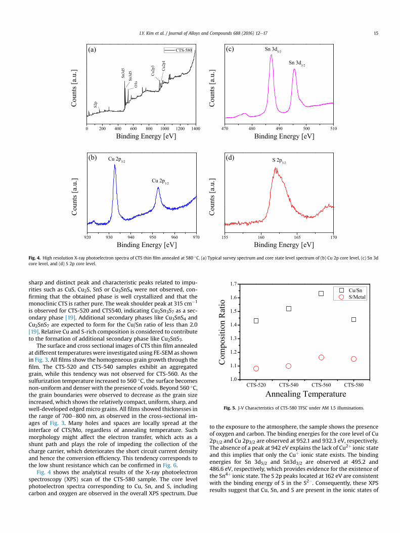
Fig. 4. High resolution X-ray photoelectron spectra of CTS thin film annealed at 580 �C. (a) Typical survey spectrum and core state level spectrum of (b) Cu 2p core level, (c) Sn 3dcore level, and (d) S 2p core level.
CTS-520 CTS-540 CTS-560 CTS-5801.0
1.1
1.2
1.3
1.4
1.5
1.6
1.7
Com
posi
tion
Rat
io
Annealing Temperature
Cu/Sn S/Metal
Fig. 5. J-V Characteristics of CTS-580 TFSC under AM 1.5 illuminations.
I.Y. Kim et al. / Journal of Alloys and Compounds 688 (2016) 12e17 15
sharp and distinct peak and characteristic peaks related to impu-rities such as CuS, Cu2S, SnS or Cu3SnS4 were not observed, con-firming that the obtained phase is well crystallized and that themonoclinic CTS is rather pure. The weak shoulder peak at 315 cm�1
is observed for CTS-520 and CTS540, indicating Cu2Sn3S7 as a sec-ondary phase [19]. Additional secondary phases like Cu3SnS4 andCu2SnS7 are expected to form for the Cu/Sn ratio of less than 2.0[19]. Relative Cu and S-rich composition is considered to contributeto the formation of additional secondary phase like Cu2SnS7.
The surface and cross sectional images of CTS thin film annealedat different temperatures were investigated using FE-SEM as shownin Fig. 3. All films show the homogeneous grain growth through thefilm. The CTS-520 and CTS-540 samples exhibit an aggregatedgrain, while this tendency was not observed for CTS-560. As thesulfurization temperature increased to 560 �C, the surface becomesnon-uniform and denser with the presence of voids. Beyond 560 �C,the grain boundaries were observed to decrease as the grain sizeincreased, which shows the relatively compact, uniform, sharp, andwell-developed edgedmicro grains. All films showed thicknesses inthe range of 700e800 nm, as observed in the cross-sectional im-ages of Fig. 3. Many holes and spaces are locally spread at theinterface of CTS/Mo, regardless of annealing temperature. Suchmorphology might affect the electron transfer, which acts as ashunt path and plays the role of impeding the collection of thecharge carrier, which deteriorates the short circuit current densityand hence the conversion efficiency. This tendency corresponds tothe low shunt resistance which can be confirmed in Fig. 6.
Fig. 4 shows the analytical results of the X-ray photoelectronspectroscopy (XPS) scan of the CTS-580 sample. The core levelphotoelectron spectra corresponding to Cu, Sn, and S, includingcarbon and oxygen are observed in the overall XPS spectrum. Due
to the exposure to the atmosphere, the sample shows the presenceof oxygen and carbon. The binding energies for the core level of Cu2p1/2 and Cu 2p3/2 are observed at 952.1 and 932.3 eV, respectively.The absence of a peak at 942 eV explains the lack of Cu2þ ionic stateand this implies that only the Cuþ ionic state exists. The bindingenergies for Sn 3d5/2 and Sn3d3/2 are observed at 495.2 and486.6 eV, respectively, which provides evidence for the existence ofthe Sn4þ ionic state. The S 2p peaks located at 162 eV are consistentwith the binding energy of S in the S2�. Consequently, these XPSresults suggest that Cu, Sn, and S are present in the ionic states of
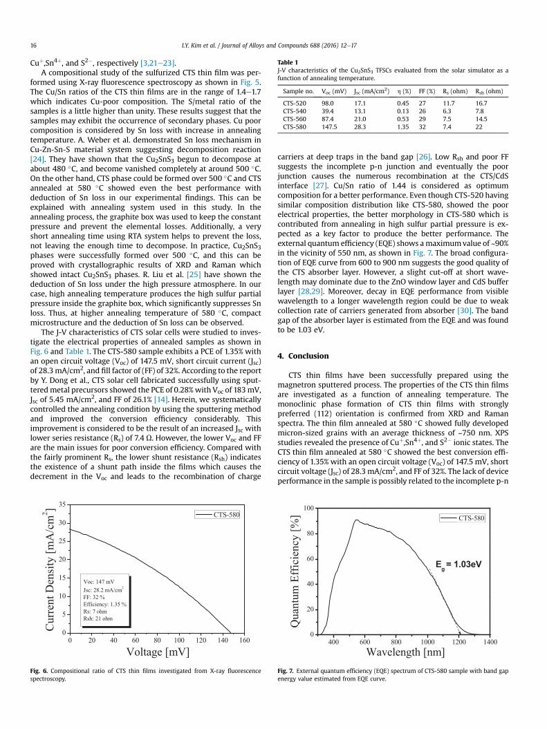
Table 1J-V characteristics of the Cu2SnS3 TFSCs evaluated from the solar simulator as afunction of annealing temperature.
Sample no. Voc (mV) Jsc (mA/cm2) h (%) FF (%) Rs (ohm) Rsh (ohm)
CTS-520 98.0 17.1 0.45 27 11.7 16.7CTS-540 39.4 13.1 0.13 26 6.3 7.8CTS-560 87.4 21.0 0.53 29 7.5 14.5CTS-580 147.5 28.3 1.35 32 7.4 22
I.Y. Kim et al. / Journal of Alloys and Compounds 688 (2016) 12e1716
Cuþ,Sn4þ, and S2�, respectively [3,21e23].A compositional study of the sulfurized CTS thin film was per-
formed using X-ray fluorescence spectroscopy as shown in Fig. 5.The Cu/Sn ratios of the CTS thin films are in the range of 1.4e1.7which indicates Cu-poor composition. The S/metal ratio of thesamples is a little higher than unity. These results suggest that thesamples may exhibit the occurrence of secondary phases. Cu poorcomposition is considered by Sn loss with increase in annealingtemperature. A. Weber et al. demonstrated Sn loss mechanism inCu-Zn-Sn-S material system suggesting decomposition reaction[24]. They have shown that the Cu2SnS3 begun to decompose atabout 480 �C, and become vanished completely at around 500 �C.On the other hand, CTS phase could be formed over 500 �C and CTSannealed at 580 �C showed even the best performance withdeduction of Sn loss in our experimental findings. This can beexplained with annealing system used in this study. In theannealing process, the graphite box was used to keep the constantpressure and prevent the elemental losses. Additionally, a veryshort annealing time using RTA system helps to prevent the loss,not leaving the enough time to decompose. In practice, Cu2SnS3phases were successfully formed over 500 �C, and this can beproved with crystallographic results of XRD and Raman whichshowed intact Cu2SnS3 phases. R. Liu et al. [25] have shown thededuction of Sn loss under the high pressure atmosphere. In ourcase, high annealing temperature produces the high sulfur partialpressure inside the graphite box, which significantly suppresses Snloss. Thus, at higher annealing temperature of 580 �C, compactmicrostructure and the deduction of Sn loss can be observed.
The J-V characteristics of CTS solar cells were studied to inves-tigate the electrical properties of annealed samples as shown inFig. 6 and Table 1. The CTS-580 sample exhibits a PCE of 1.35% withan open circuit voltage (Voc) of 147.5 mV, short circuit current (Jsc)of 28.3mA/cm2, and fill factor of (FF) of 32%. According to the reportby Y. Dong et al., CTS solar cell fabricated successfully using sput-teredmetal precursors showed the PCE of 0.28%with Voc of 183mV,Jsc of 5.45 mA/cm2, and FF of 26.1% [14]. Herein, we systematicallycontrolled the annealing condition by using the sputtering methodand improved the conversion efficiency considerably. Thisimprovement is considered to be the result of an increased Jsc withlower series resistance (Rs) of 7.4 U. However, the lower Voc and FFare the main issues for poor conversion efficiency. Compared withthe fairly prominent Rs, the lower shunt resistance (Rsh) indicatesthe existence of a shunt path inside the films which causes thedecrement in the Voc and leads to the recombination of charge
0 20 40 60 80 100 120 140 1600
5
10
15
20
25
30
35
Cur
rent
Den
sity
[mA
/cm
2 ]
Voltage [mV]
Voc: 147 mVJsc: 28.2 mA/cmFF: 32 %Efficiency: 1.35 %Rs: 7 ohmRsh: 21 ohm
CTS-580
Fig. 6. Compositional ratio of CTS thin films investigated from X-ray fluorescencespectroscopy.
carriers at deep traps in the band gap [26]. Low Rsh and poor FFsuggests the incomplete p-n junction and eventually the poorjunction causes the numerous recombination at the CTS/CdSinterface [27]. Cu/Sn ratio of 1.44 is considered as optimumcomposition for a better performance. Even though CTS-520 havingsimilar composition distribution like CTS-580, showed the poorelectrical properties, the better morphology in CTS-580 which iscontributed from annealing in high sulfur partial pressure is ex-pected as a key factor to produce the better performance. Theexternal quantum efficiency (EQE) shows amaximumvalue of ~90%in the vicinity of 550 nm, as shown in Fig. 7. The broad configura-tion of EQE curve from 600 to 900 nm suggests the good quality ofthe CTS absorber layer. However, a slight cut-off at short wave-length may dominate due to the ZnO window layer and CdS bufferlayer [28,29]. Moreover, decay in EQE performance from visiblewavelength to a longer wavelength region could be due to weakcollection rate of carriers generated from absorber [30]. The bandgap of the absorber layer is estimated from the EQE and was foundto be 1.03 eV.
4. Conclusion
CTS thin films have been successfully prepared using themagnetron sputtered process. The properties of the CTS thin filmsare investigated as a function of annealing temperature. Themonoclinic phase formation of CTS thin films with stronglypreferred (112) orientation is confirmed from XRD and Ramanspectra. The thin film annealed at 580 �C showed fully developedmicron-sized grains with an average thickness of ~750 nm. XPSstudies revealed the presence of Cuþ,Sn4þ, and S2� ionic states. TheCTS thin film annealed at 580 �C showed the best conversion effi-ciency of 1.35% with an open circuit voltage (Voc) of 147.5 mV, shortcircuit voltage (Jsc) of 28.3 mA/cm2, and FF of 32%. The lack of deviceperformance in the sample is possibly related to the incomplete p-n
400 600 800 1000 1200 14000
20
40
60
80
100
Qua
ntum
Eff
icie
ncy
[%]
Wavelength [nm]
Eg = 1.03eV
CTS-580
Fig. 7. External quantum efficiency (EQE) spectrum of CTS-580 sample with band gapenergy value estimated from EQE curve.

I.Y. Kim et al. / Journal of Alloys and Compounds 688 (2016) 12e17 17
junction formation. This indicates a better efficiency for CTS solarcell fabricated using a sputtering method, which demonstrates theeffectiveness of the sputtering method for the fabrication of CTSbased TFSCs.
Acknowledgment
This research was financially supported by Basic ScienceResearch Program through the National Research Foundation ofKorea (NRF) funded by the Ministry of Science, ICT and FuturePlanning (NRF-2015R1A2A2A01006856) and the Human ResourcesDevelopment Program (No.:20124010203180) of the Korea Insti-tute of Energy Technology Evaluation and Planning (KETEP) grantfunded by the Korea Government Ministry of Trade, Industry andEnergy.
References
[1] N. Aihara, H. Araki, A. Takeuchi, K. Jimbo, H. Katagiri, Fabrication of Cu2SnS3thin films by sulfurization of evaporated Cu-Sn precursors for solar cells, Phys.Status Solidi C 10 (2013) 1086e1092.
[2] K. Ayaka, T. Kotoba, C. Kotaro, K. Hironori, A. Hideaki, Fabrication of Cu2SnS3thin-film solar cells with power conversion efficiency of over 4%, Jpn. J. Appl.Phys 54 (2015) 08KC06.
[3] T. Srinivasa Reddy, R. Amiruddin, M.C. Santhosh Kumar, Deposition andcharacterization of Cu2SnS3 thin films by co-evaporation for photovoltaicapplication, Sol. Energy Mater. Sol. Cells 143 (2015) 128e134.
[4] C. Kotaro, K. Junpei, E. Shinya, A. Hideaki, N. Ryota, J. Kazuo, K. Hironori,Preparation of Cu2SnS3 thin films by sulfurization of Cu/Sn stacked precursors,Jpn. J. Appl. Phys. 51 (2012) 10NC35.
[5] A.C. Lokhande, K.V. Gurav, E. Jo, C.D. Lokhande, J.H. Kim, Chemical synthesis ofCu2SnS3 (CTS) nanoparticles: a status review, J. Alloys Compd. 656 (2016)295e310.
[6] N. Mitsuki, F. Junya, Y. Toshiyuki, I. Masanobu, Cu2SnS3 thin-film solar cellsfabricated by sulfurization from NaF/Cu/Sn stacked precursor, Appl. Phys.Express 8 (2015) 042303.
[7] R. Bodeux, J. Leguay, S. Delbos, Influence of composition and annealing on thecharacteristics of Cu2SnS3 thin films grown by cosputtering at room temper-ature, Thin Solid Films 582 (2015) 229e232.
[8] Q. Liu, Z. Zhao, Y. Lin, P. Guo, S. Li, D. Pan, X. Ji, Alloyed (ZnS)x(Cu2SnS3)1-x and(CuInS2)x(Cu2SnS3)1-x nanocrystals with arbitrary composition and broadtunable band gaps, Chem. Commun. 47 (2011) 964e966.
[9] D. Avellaneda, M.T.S. Nair, P.K. Nair, Cu2SnS3 and Cu4SnS4 thin films viachemical deposition for photovoltaic application, J. Electrochem. Soc. 157(2010) D346eD352.
[10] H. Guan, H. Shen, C. Gao, X. He, Structural and optical properties of Cu2SnS3and Cu3SnS4 thin films by successive ionic layer adsorption and reaction,J. Mater. Sci. Mater. Electron. 24 (2013) 1490e1494.
[11] A. Kanai, H. Araki, A. Takeuchi, H. Katagiri, Annealing temperature depen-dence of photovoltaic properties of solar cells containing Cu2SnS3 thin filmsproduced by co-evaporation, Phys. Status Solidi B 252 (2015) 1239e1243.
[12] M. Xie, D. Zhuang, M. Zhao, Z. Zhuang, L. Ouyang, X. Li, J. Song, Preparation andcharacterization of Cu2ZnSnS4 thin films and solar cells fabricated from
quaternary Cu-Zn-Sn-S target, Int. J. Photoenergy 2013 (2013) 9.[13] M.P. Suryawanshi, G.L. Agawane, S.M. Bhosale, S.W. Shin, P.S. Patil, J.H. Kim,
A.V. Moholkar, CZTS based thin film solar cells: a status review, Mater.Technol. 28 (2013) 98e109.
[14] Y. Dong, J. He, L. Sun, Y. Chen, P. Yang, J. Chu, Effect of sulfurization temper-ature on properties of Cu2SnS3 thin films and solar cells prepared by sulfu-rization of stacked metallic precursors, Mater. Sci. Semicond. Process 38(2015) 171e176.
[15] Z. Su, K. Sun, Z. Han, F. Liu, Y. Lai, J. Li, Y. Liu, Fabrication of ternary Cu-Sn-Ssulfides by a modified successive ionic layer adsorption and reaction(SILAR) method, J. Mater. Chem. 22 (2012) 16346e16352.
[16] H. Dahman, S. Rabaoui, A. Alyamani, L. El Mir, Structural, morphological andoptical properties of Cu2SnS3 thin film synthesized by spin coating technique,Vacuum 101 (2014) 208e211.
[17] D. Tiwari, T.K. Chaudhuri, T. Shripathi, U. Deshpande, R. Rawat, Non-toxic,earth-abundant 2% efficient Cu2SnS3 solar cell based on tetragonal filmsdirect-coated from single metal-organic precursor solution, Sol. Energy Mater.Sol. Cells 113 (2013) 165e170.
[18] P.A. Fernandes, P.M.P. Salom�e, A.F. da Cunha, CuxSnSxþ1 (x ¼ 2, 3) thin filmsgrown by sulfurization of metallic precursors deposited by dc magnetronsputtering, Phys. Status Solidi C 7 (2010) 901e904.
[19] D.M. Berg, R. Djemour, L. Gütay, S. Siebentritt, P.J. Dale, X. Fontane,V. Izquierdo-Roca, A. P�erez-Rodriguez, Raman analysis of monoclinic Cu2SnS3thin films, Appl. Phys. Lett. 100 (2012) 192103.
[20] N.R. Mathews, J. Tamy Benítez, F. Paraguay-Delgado, M. Pal, L. Huerta, For-mation of Cu2SnS3 thin film by the heat treatment of electrodeposited SnSeCulayers, J. Mater. Sci. Mater. Electron. 24 (2013) 4060e4067.
[21] J. Han, Y. Zhou, Y. Tian, Z. Huang, X. Wang, J. Zhong, Z. Xia, B. Yang, H. Song,J. Tang, Hydrazine processed Cu2SnS3 thin film and their application forphotovoltaic devices, Front. Optoelectron. 7 (2014) 37e45.
[22] B. Li, Y. Xie, J. Huang, Y. Qian, Synthesis, characterization, and properties ofnanocrystalline Cu2SnS3, J. Solid State Chem. 153 (2000) 170e173.
[23] S.A. Vanalakar, G.L. Agawane, S.W. Shin, H.S. Yang, P.S. Patil, J.Y. Kim, J.H. Kim,Non-vacuummechanochemical route to the synthesis of Cu2SnS3 nano-ink forsolar cell applications, Acta Mater. 85 (2015) 314e321.
[24] A. Weber, R. Mainz, H.W. Schock, On the Sn loss from thin films of the materialsystem CueZneSneS in high vacuum, J. Appl. Phys. 107 (2010) 013516.
[25] R. Liu, M. Tan, L. Xu, X. Zhang, J. Chen, X. Tang, Preparation of high-qualityCu2ZnSnS4 thin films for solar cells via the improvement of sulfur partialpressure using a static annealing sulfurization approach, Sol. Energy Mater.Sol. Cells 157 (2016) 221e228.
[26] S.A. Vanalakar, G.L. Agawane, A.S. Kamble, C.W. Hong, P.S. Patil, J.H. Kim,Fabrication of Cu2SnS3 thin film solar cells using pulsed laser depositiontechnique, Sol. Energy Mater. Sol. Cells 138 (2015) 1e8.
[27] M. Cao, L. Li, B.L. Zhang, J. Huang, L.J. Wang, Y. Shen, Y. Sun, J.C. Jiang, G.J. Hu,One-step deposition of Cu2ZnSnS4 thin films for solar cells, Sol. Energy Mater.Sol. Cells 117 (2013) 81e86.
[28] M.P. Suryawanshi, U.V. Ghorpade, S.W. Shin, S.A. Pawar, I.Y. Kim, C.W. Hong,M. Wu, P.S. Patil, A.V. Moholkar, Jin Hyeok Kim, A simple aqueous precursorsolution processing of earth-abundant Cu2SnS3 absorbers for thin-film solarcells, ACS Appl. Mater. Interfaces 18 (2016) 11603e11614.
[29] U.V. Ghorpade, M.P. Suryawanshi, S.W. Shin, I.Y. Kim, S.,K. Ahn, J.H. Yun,C. Jeong, S.S. Kolekar, J.J. Kim, Colloidal wurtzite Cu2SnS3 (CTS) nanocrystalsand their applications in solar cells, Chem. Mater. 28 (2016) 3308e3317.
[30] X. Liu, J. Huang, F. Zhou, F. Liu, K. Sun, C. Yan, J.A. Stride, X. Hao, Understandingthe key factors of enhancing phase and compositional controllability for 6%efficient pure-sulfide Cu2ZnSnS4 solar cells prepared from quaternary wurt-zite nanocrystals, Chem. Mater. 28 (2016) 3649e3658.