journal of lightwave technology, vol. 31, no....
TRANSCRIPT

JOURNAL OF LIGHTWAVE TECHNOLOGY, VOL. 31, NO. 24, DECEMBER 15, 2013 3943
Analysis and Design of Microring-Based SwitchingElements in a Silicon Photonic Integrated
Transponder AggregatorPaolo Pintus, Member, IEEE, Pietro Contu, Nicola Andriolli, Antonio D’Errico,
Fabrizio Di Pasquale, Member, IEEE, and Francesco Testa
Abstract—In this paper, we present and investigate a new archi-tecture of a silicon photonic transponder aggregator as a new in-terconnect subsystem enabling the implementation of colorless, di-rectionless, and contentionless ROADMs. Such subsystem is basedon a microring resonator switching fabric integrated in a siliconphotonics platform to achieve high functional integration togetherwith reduction of cost, footprint, and power consumption. In theproposed device, microring resonators perform simultaneous addand drop of wavelength channels which suffer from two detrimen-tal effects: residual dropped signal crosstalk and residual addedsignal crosstalk, respectively. Considering three microring-basedswitching elements, the transfer matrix method has been used tocompute the add/drop transfer functions of the switches as a func-tion of their geometrical parameters. The two crosstalk effects havebeen evaluated jointly with other important transmission param-eters, such as bandwidth, insertion losses, side lobe suppression,adjacent channel rejection, extinction ratio, and group dispersion.In addition, device sensitivity with respect to the ring-waveguidecoupling coefficients has been calculated. Finally, the performanceof the different switches has been assessed to demonstrate that,by a proper design, the proposed transponder aggregator cansupport 100 Gb/s DP-QPSK modulated signal transmission.
Index Terms—Integrated optics, optical switches, ringresonators.
I. INTRODUCTION
DYNAMIC rearrangement of capacity while optimizingtransport resources utilization and further lowering capital
cost and power consumption is a fundamental requirement fornext generation optical transport networks. These features canbe ensured by implementing highly flexible transport nodes inconjunction with an intelligent control and management planeempowering software defined networking (SDN) [1].
Conventional reconfigurable optical add and drop multiplexer(ROADM) nodes are implemented using broadcast-and-selectarchitecture. Fig. 1 shows a four-directional ROADM based on
Manuscript received June 14, 2013; revised July 31, 2013; accepted August1, 2013. Date of publication August 5, 2013; date of current version November27, 2013.
P. Pintus, P. Contu, N. Andriolli, and F. Di Pasquale are with theScuola Superiore Sant’Anna, 56124 Pisa, Italy (e-mail: [email protected];[email protected]; [email protected]; [email protected]).
A. D’Errico and F. Testa are with the Ericsson S.p.A, 56124 Pisa, Italy(e-mail: [email protected]; [email protected]).
Color versions of one or more of the figures in this paper are available onlineat http://ieeexplore.ieee.org.
Digital Object Identifier 10.1109/JLT.2013.2276852
Fig. 1. Conventional ROADM architecture.
two main system blocks: the optical line switching section andthe local add and drop section. The former comprises, for eachdirection, a N × 1 (with N equal to the node directions) wave-length selective switching (WSS) module to selectively combineonto the output fiber the wavelengths distributed by the differ-ent power splitters (PS). Local add and drop section includesarrayed waveguide gratings (AWG) to interconnect the opticalline switch to fixed wavelength transponders (Tx modules inFig. 1). For signal dropping, an array of AWG demultiplexersis used to separate the signals distributed by the power splitterin each network direction before reception at the receivers (Rxmodules). Similarly, another AWG array is used to multiplex thelocally generated signals to be added to each network direction.In such conventional nodes, full switching flexibility is only en-sured for wavelength channels in transit across the node towardother nodes. Actually these channels can be routed from any toany direction. On the contrary, added and dropped wavelengthsare rigidly assigned to a fixed direction and to a fixed color (bymeans of WDM multiplexer and demultiplexer array) and anychange in these configurations must be performed by manualrewiring [2].
Next generation ROADM should provide higher flexibil-ity with respect to currently deployed optical nodes. In suchnew nodes, the routing of added/dropped wavelength channelsto/from any direction should be guaranteed without any manualintervention (directionless operation), independently from thetransponder wavelength (colorless operation) and by allowing
0733-8724 © 2013 IEEE
3944 JOURNAL OF LIGHTWAVE TECHNOLOGY, VOL. 31, NO. 24, DECEMBER 15, 2013
multiple transponders operating at the same wavelength to behandled by the same add and drop section (contentionless op-eration) [3], [4]. In order to address these new requirementswithout significantly increasing cost, footprint, and complex-ity, photonic integrated devices will play a crucial role. Thearchitecture of a new silicon photonic system on chip (SoC) ispresented and investigated.
The paper is organized as follows: in Section II, the conceptof a colorless directionless contentionless (CDC) ROADM is in-troduced and a new integrated device as transponder aggregator(TPA) is presented and discussed in Section III. The proposedTPA architecture is based on a switching fabric, which canbe performed using silicon microring resonators on a silicon-on-isolator (SOI) platform. In this study, three switching ele-ments are investigated, which are presented in Section IV. Arigorous mathematical model of such switches is introduced inSection V, followed by the simulation results, which are illus-trated in Section VI. By considering the relevant features of aring-based switching element (i.e., the full width at half max-imum bandwidth, the insertion losses, the side lobe suppres-sion, the adjacent channel rejection, the extinction ratio, andthe group dispersion), we have shown that only one of the threeswitch configurations meets all the identified requirements. Thisswitch is made up of two waveguides, crossing at an angle θ, andtwo rings located on the opposite side of the waveguide cross-ing. Optimizing the ring-waveguide coupling coefficient and theangle θ, we verified that such a switching element can supporthigh speed transmission. The TPA performance is eventuallydiscussed in Section VII and in Section VIII, the conclusionsare drawn.
II. CDC ROADM NODES
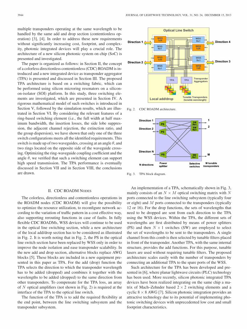
The colorless, directionless and contentionless operations inthe ROADM nodes (CDC ROADM) will give the possibilityto optimize the resource utilization, to reconfigure network ac-cording to the variation of traffic pattern in a cost effective way,also supporting rerouting functions in case of faults. In fullyflexible CDC ROADMs, WSS devices will continue to be usedin the optical line switching section, while a new architectureof the local add/drop section has to be considered as illustratedin Fig. 2. It is worth noting that in Fig. 2, the PS in the opticalline switch section have been replaced by WSS only in order toimprove the node isolation and ease transponder scalability. Inthe new add and drop section, alternative blocks replace AWGblocks [5]. These blocks are included in a new equipment pre-sented in this paper as TPA. For the add (drop) function theTPA selects the direction to which the transponder wavelengthhas to be added (dropped) and combines it together with thewavelengths to be added (dropped) to the same direction fromother transponders. To compensate for the TPA loss, an arrayof N optical amplifiers (not shown in Fig. 2) is required at theinterface of the TPA to the optical line switch.
The function of the TPA is to add the required flexibility atthe end point, between the line switching subsystem and thetransponder subsystem.
Fig. 2. CDC ROADM architecture.
Fig. 3. TPA block diagram.
An implementation of a TPA, schematically shown in Fig. 3,mainly consists of an N × M optical switching matrix with Nports connected to the line switching subsystem (typically fouror eight) and M ports connected to the transponders (typically12 or 16). For the drop functions, the sets of wavelengths thatneed to be dropped are sent from each direction to the TPAusing the WSS devices. Within the TPA, the different sets ofwavelengths are first distributed by means of power splitters(PS) and then N × 1 switches (SW) are employed to selectthe set of wavelengths to be sent to the transponders. A singlechannel from this comb is then selected by tunable filters placedin front of the transponder. Another TPA, with the same internalstructure, provides the add functions. For this purpose, tunablelasers are used without requiring tunable filters. The proposedarchitecture scales easily with the number of transponders byconnecting an additional TPA to the spare ports of the WSS.
Such architecture for the TPA has been developed and pre-sented in [6], where planar lightwave circuits (PLC) technologyhas been used. More recently, silicon photonic integrated TPAdevices have been realized integrating on the same chip a ma-trix of Mach–Zehnder based 2 × 2 switching elements and acyclic 8 × 8 AWG [7]. Silicon photonic integration provides anattractive technology due to its potential of implementing pho-tonic switching devices with unprecedented low cost and smallfootprint characteristics.

PINTUS et al.: ANALYSIS AND DESIGN OF MICRORING-BASED SWITCHING ELEMENTS 3945
Fig. 4. Conceptual TPA block diagram.
III. SILICON PHOTONICS INTEGRATED TPA
The SoC TPA proposed in this paper is based on silicon pho-tonics technology and uses a scalable matrix of color-coded mi-croring resonator switching elements in conjunction with WDMmultiplexers and demultiplexers. The conceptual architecture ofthe TPA is shown in Fig. 4. According to this architecture, a sin-gle switching matrix is used for both add and drop functions.The matrix has dimension NK × M , where N is the numberof fibers (i.e., N = 4), K is the number of wavelengths perfiber (i.e., K = 48), and M is the number of ports connectedto transponders (i.e., M = 12). The matrix is placed betweenAWG multiplexer and demultiplexer elements.
Tunable transmitters are connected at the top of the matrix andthe wavelength channels to be added proceed vertically alongone column crossing many switching elements until they areeventually horizontally switched. The switching occurs at theelementary switch corresponding to the color of the signal andto the direction to which it must be added. The signal eventuallyarrives at the input of the wavelength multiplexer.
For the drop function, the wavelengths to be dropped passthrough a wavelength demultiplexer, and then, proceed hori-zontally along the color-coded rows until they are verticallyswitched by the switching elements in the column of the se-lected receivers. They proceed vertically across many switchingelements until they arrive to the receivers connected at the bot-tom of the switching matrix as shown in Fig. 4.
Fig. 4 reports an example where the dotted blue line representsa wavelength to be added to direction 2 by the transponder Tx 3,working at color λK , and simultaneously, a signal at the samecolor λK (represented by the dotted red line) must be droppedfrom the same direction 2 at the transponder Rx 3. This examplepoints out that the TPA can perform simultaneously both add
and drop operations by activating the same switching element.As a matter of fact, the same switching element, driven to switchhorizontally a given added channel coming from the top, is ableto switch vertically the same wavelength that comes from theleft.
It is worth noting that only M (e.g., 12 or 16) channels areinjected in the TPA by the N input directions. Indeed, the WSSsselect only the channels that must be added/dropped, which areat maximum equal to the number of transponders. Let us alsoobserve that for this goal just one switch in each column needsto be locked, while the rest of the rings are simply put out ofband to let the signal pass transparently.
To perform the control of the switching elements in closedloop, integrated photodetectors can be located at the drop ports.Thermal heaters can be effectively used to trim the resonance ofthe rings [8], allowing to switch ON (i.e., ring resonance alignedwith the selected channel) and OFF (i.e., ring resonance shiftedwith respect to the channels) the switching elements. Designingproperly the location and the size of the heaters as well as thespacing and the configuration of the rings, allows to stronglyminimize the thermal crosstalk amongst the switches, which isdefined as the phase change ratio induced by the closest ring-based switch due to the heated switch. It has been proved thata distance larger than 15μm and thermal isolation trenches cansuccessfully reduce the thermal crosstalk [9]. Moreover, in ourdevice all the crosspoint switches are uniquely designed for theirparticular wavelength and the rings need just a small heat to beswitched ON/OFF and to be trimmed in order to compensate thefabrication errors. As a result, the variation of the temperatureacross the chip will be limited as well as the thermal crosstalk.
As it is well known, due to material stress and waveguidegeometry, polarization birefringence occurs in silicon planarwaveguide components. In order to preserve polarization infor-mation, polarization diversity configuration must be designed.For this reason, polarization splitters and rotators must be con-sidered at the input/output of the device.
IV. MICRORING-BASED SWITCHING ELEMENTS
To implement such an integrated TPA, different microringswitching element configurations can be considered, each char-acterized by different performances. The most relevant ones areshown in Fig. 5.
The simplest ring-based switching element is constituted bya single microring placed on one corner of the waveguide cross-ing as shown in Fig. 5(a) [10]. Let IN and OUT be the inputand the output direction of the network, while Add and Dropare the local ports for adding/dropping a single channel to/fromtransponders. When a WDM signal is propagating from IN toOUT and the resonance wavelength of the ring matches a wave-length carrier, that channel can be dropped to the Drop port andreplaced by a new one coming from the Add port. It is worthnoting that the add/drop functions work simultaneously at thesame wavelength. For this reason, we have introduced and in-vestigated two new important parameters defined as the residualdropped signal crosstalk (CR.D.) and the residual added signalcrosstalk (CR.A.). The CR.D. is measured at the OUT port and

3946 JOURNAL OF LIGHTWAVE TECHNOLOGY, VOL. 31, NO. 24, DECEMBER 15, 2013
Fig. 5. Three microring configurations under investigation. (a) Two-waveguide add/drop switch with a single ring. (b) Three-waveguide add/dropswitch with a single ring. (c) Two-waveguide add/drop switch with two rings.
is defined as the ratio between the remaining part of the droppedsignal and the added signal. Vice versa, the CR.A. is the ratiobetween the remaining part of the added signal and the droppedsignal at the Drop port. Let us note that when a new signal isinjected from the Add port, it is expected to be completely sentto the OUT port; however, it is also partially coupled to theDrop port. For the switching element in Fig. 5(a), the interfer-ence between the added signal and the dropped signal at Dropport might be very high because the add and drop ports are onthe opposite ends of the same waveguide. Note that while thedropped signal is usually quite low in terms of power becausecoming from the network (e.g., −15 dBm or lower), the addedsignal might be much larger because it has just been generatedby a tunable transponder (e.g., 5 dBm or even higher). Due tothis fact, the two signals are quite unbalanced in terms of powerand a CR.A. smaller than −40 dB is then needed. It is worth tonote that those two crosstalk effects are the contributor of thecoherent (same wavelength) crosstalk.
A slightly modified version of the aforementioned configura-tion is depicted Fig. 5(b), where a single ring is placed betweentwo waveguide crossings, and add/drop ports are placed at theend of two separated waveguides in order to minimize the issuesof the former switching element.
Alternatively, we can add another ring to the switch inFig. 5(a). The new switching element is shown in Fig. 5(c),where two resonators are placed on the opposite corners of thewaveguide crossing [11]. Note that while the first ring mainlyperforms the drop function, the second one is mostly responsi-ble of the adding. Concerning this structure, in this study, we
Fig. 6. Relevant features of a ring-based switch: full-width at half-maximumbandwidth (FWHM), the insertion loss (IL), the side lobe suppression (SLS),and the adjacent channel rejection (ChR).
have introduced an extra degree of freedom by varying the an-gle between the two waveguides. The result of using two ringsis to enlarge the coupling, and consequently, to decrease thecrosstalk.
Let us note that the switching element in Fig. 5(a) can beseen as a special case of the one shown in Fig. 5(c), when thesecond ring has been removed or it is not coupled to the twowaveguides. As a consequence, in the following, we will focuson the mathematical model of the second and third switches,because the first structure can be easily derived.
In addition to the two previously defined crosstalk effects,the performance of the ring-based switches has been evalu-ated also in terms of the full-width at half-maximum bandwidth(FWHM ), the drop insertion loss (ILd ), the side lobe suppres-sion (SLS), and the adjacent channel rejection (ChR), whichare schematically shown in Fig. 6. Let us also note that the sidelobes do not appear when a single ring is used.
The ChR is a quite important parameter to evaluate the per-formance of the device in WDM applications. In this paper,the ChR has been evaluated considering a channel spacing of100 GHz, however larger channel spacing (i.e., 200 GHz) willproduce higher rejection.
Varying the refractive index by thermal heating, the ring reso-nance can be shifted, switching ON and OFF the correspondingcrosspoint. To evaluate the performance of the switching be-tween the two states, two parameters have been considered: theextinction ratio (ER) and the bypass insertion loss (ILbp ). Theformer is defined as the ratio of the optical power between theON and OFF states, while the latter is the loss when the ring isout of resonance (OFF state), both shown in Fig. 7(a) and (b),respectively. For the sake of clarity, in the plots of Fig. 7, wehave not considered the side lobes.
A high value of ER is fundamental to reduce the incoherentcrosstalk, which is the sum of the contribution of all the in-tervening channels. To explain its importance, let us recall thatonly one ring is resonating in each vertical path, while the othersare out of resonance. If they are not switched OFF completely,part of the other channels, which are propagating horizontally,can be partially dropped resulting in an incoherent noise on

PINTUS et al.: ANALYSIS AND DESIGN OF MICRORING-BASED SWITCHING ELEMENTS 3947
Fig. 7. Extinction ratio (ER) and Bypass Insertion Loss (ILbp ) for a ring-based switch in an OFF state. (a) Drop function. (b) Through function.
the wanted signal. Assuming a uniform ER and M channels,the incoherent total power from the intervening channels willbe 10 log10(M − 1) dB higher. In our case, for M = 12, thatvalue is about 11 dB. To guarantee a small incoherent crosstalk,an ER higher than 35 dB is then needed. However, this con-straint can be relaxed by filtering out all the incoherent noisewith an integrated tunable filter, as a result lower ER are per-mitted. Vice versa, a low ILbp allows a signal to pass throughthe switch without been attenuated. To complete our analysis,we will also explore the dispersion induced by the drop andthrough transfer functions.
In the following, we will investigate and optimize the switch-ing elements in terms of the ring-waveguide coupling coef-ficients and also in terms of the angle θ for the two-ringconfiguration.
Ring-waveguide couplers and waveguide crossings may af-fect the network performance introducing loss, crosstalk, andbandwidth limitation [12]. Vice versa, waveguide propagationloss is usually sufficiently low to support global interconnectionon the chip due to the small size of the device. In this study, wewill focus our attention on the influence of ring-waveguide cou-pling, while we assume that the effect of waveguide crossingsis negligible. This choice is supported by the fact that compactstructures like mode-field expanders can guarantee a crosstalklower than −45 dB in a broad wavelength range [13], [14]. Foreach waveguide crossing, an insertion loss as low as 0.16 dB hasbeen reported, which might not be negligible after a cascade ofseveral crossings. That loss can be effectively compensated byusing integrated hybrid semiconductor optical amplifiers withinthe TPA [15], [16].
Fig. 8. Top-view of the three-waveguide add/drop switch.
Evaluating the previous configurations, we show that onlythe two-waveguide switch with two rings satisfies the designconstraint for our TPA application.
V. MATHEMATICAL MODEL
The transfer function of the devices is computed using thetransfer matrix method [17], [18]. Assuming lossless couplers,the field cross-coupling coefficient and the field transmissioncoefficient at the ring-waveguide coupling area are k = j
√K
and t =√
1 − K, respectively, where K is the ring-waveguidepower coupling ratio. The code has been also validated with theresults shown in [18].
In this study, we have considered 420 nm × 220 nm TEsingle-mode silicon waveguides, manufactured on a SOI plat-form. In our analysis, βwg and αwg are the waveguide phase andattenuation constants, whereas βrr and αrr are the phase and theattenuation constants for the ring, respectively. The phase con-stants βwg/rr have been computed using a full-vectorial finite-element solver [19], [20], while the attenuation values αwg/rr
have been taken from the literature [21].Assuming R the ring radius, let us also introduce τ =
exp[−(αrr − jβrr )2πR] as the ring round-trip transmissionfactor. Its amplitude is related to the ring-loss (|τ | = 1 meanslossless resonator) and its phase is the ring round-trip phasechange. For example, the term τ 1/4 represents the field compo-nent that propagates along a quarter of the ring.
A. Three-Waveguide Switch
Referring to Fig. 8, we use the capital letters for the signalspropagating in the waveguides and the lower case for the corre-sponding waves in the ring. Let (A,C,E) be the ingoing wavesto Coupler1 , Coupler2 and Coupler3 , respectively, while theoutgoing signals are (B,D,F ). The corresponding ingoing-coupler and outgoing-coupler waves in the ring are (a, c, e) and(b, d, f), respectively. Using the relations in [17], we have
(B
b
)=
(t1 k1
−k∗1 t∗1
)(A
a
),
(D
d
)=
(t2 k2
−k∗2 t∗2
)(C
c
)
(F
f
)=
(t3 k3
−k∗3 t∗3
)(E
e
). (1)

3948 JOURNAL OF LIGHTWAVE TECHNOLOGY, VOL. 31, NO. 24, DECEMBER 15, 2013
Fig. 9. Top-view of the two-waveguide add/drop switch.
Additionally, the waves in the ring are related by the followingphase-shift relations
c = τ 1/4b, e = τ 1/4d, a = τ 1/2f. (2)
After some algebraic manipulations, it can be shown that(B,D,F ) are linked to (A,C,E) by the following linearrelations: ⎛
⎜⎝B
D
F
⎞⎟⎠ =
⎛⎜⎝
T11 T12 T13
T21 T22 T23
T31 T32 T33
⎞⎟⎠
⎛⎜⎝
A
C
E
⎞⎟⎠ (3)
where
T11 =t1 − t∗2t
∗3(|t1 |2 + |k1 |2)τ
1 − t∗1t∗2t
∗3τ
(4a)
T22 =t2 − t∗1t
∗3(|t2 |2 + |k2 |2)τ
1 − t∗1t∗2t
∗3τ
(4b)
T33 =t3 − t∗1t
∗2(|t3 |2 + |k3 |2)τ
1 − t∗1t∗2t
∗3τ
(4c)
T12 = − k1k∗2t
∗3τ
3/4
1 − t∗1t∗2t
∗3τ
, T13 = − k1k∗3τ
1/2
1 − t∗1t∗2t
∗3τ
(4d)
T23 = − t∗1k2k∗3τ
3/4
1 − t∗1t∗2t
∗3τ
, T21 = − k∗1k2τ
1/4
1 − t∗1t∗2t
∗3τ
(4e)
T31 = − k∗1t
∗2k3τ
1/2
1 − t∗1t∗2t
∗3τ
, T32 = − k∗2k3τ
1/4
1 − t∗1t∗2t
∗3τ
. (4f)
Let us note that the previous equations hold also in the caseof lossy couplers, i.e., with (|ti |2 + |ki |2) < 1 for i = 1, 2, 3.
B. Two-Waveguide Switch
Exploiting the same approach used for the three-waveguideswitch, we can compute the transfer matrix for the second struc-ture reported in Fig. 9.
Considering the directions shown in Fig. 9, the inputs arelabeled with IN and Add, while the outputs are OUT andDrop. Using the notation reported in the figure, we have A =IN, G = Add, F = OUT and D = Drop.
Relating the input to the output waves at each coupler, we get(B
b
)=
(t1 k1
−k∗1 t∗1
)(A
a
),
(D
d
)=
(t2 k2
−k∗2 t∗2
)(C
c
)
(5a)(F
f
)=
(t3 k3
−k∗3 t∗3
)(E
e
),
(H
h
)=
(t4 k4
−k∗4 t∗4
)(G
g
)
(5b)
where (5a) and (5b) refer to the first and second ring in Fig. 9,respectively. As we did in the previous case, we have to takeinto account the phase-shift relations
c = τib, a = τed, g = τef, e = τih (6)
where τi/e = τ12 (1∓ θ
π ). In this case, we must also consider thephase delay between the two rings, which means
E = pB, C = pH. (7)
This extra phase shift parameter p = e−2(αw g −jβw g )Lw g is re-lated to the distance between the rings 2Lwg � 2R/ tan(θ/2).It can be easily shown that (F,D) are related to (A,G) by thefollowing linear relations:(
F
D
)=
(R1 T1
T2 R2
)(A
G
)(8)
where
R1 =α1α3
1 − β1β4, T1 = −
(β3 +
β1α3α4
1 − β1β4
)(9a)
R2 =α2α4
1 − β1β4, T2 = −
(β2 +
α1α2β4
1 − β1β4
)(9b)
and
α1 =t1 − t∗2(|t1 |2 + |k1 |2)τ
1 − t∗1t∗2τ
, β1 =k1k
∗2pτe
1 − t∗1t∗2τ
(10a)
α2 =t2p − t∗1(|t2 |2 + |k2 |2)pτ
1 − t∗1t∗2τ
, β2 =k∗
1k2τi
1 − t∗1t∗2τ
(10b)
α3 =t3p − t∗4(|t3 |2 + |k3 |2)pτ
1 − t∗3t∗4τ
, β3 =k3k
∗4τi
1 − t∗3t∗4τ
(10c)
α4 =t4 − t∗3(|t4 |2 + |k4 |2)τ
1 − t∗3t∗4τ
, β4 =k∗
3k4pτe
1 − t∗3t∗4τ
. (10d)
Like in the previous case, the (10a)–(10d) are also valid in thecase of lossy couplers, i.e., (|ti |2 + |ki |2) < 1 for i = 1, 2, 3, 4.Note that the transfer function for the switching element shownin Fig. 5(a) can be easily computed assuming k3 = k4 = 0, t3 =t4 = 1, and θ = 90◦.
When the signal is injected only from IN (i.e., A = 1, G =0), the output signals F (OUT ) and D (Drop) are given by thereflection and transmission coefficients R1 and T2 , respectively.Vice versa, when the signal is injected only from the Add-port(i.e., A = 0, G = 1), the output signals F (OUT ) and D (Drop)are given by the transmission and reflection coefficients T1 andR2 , respectively.

PINTUS et al.: ANALYSIS AND DESIGN OF MICRORING-BASED SWITCHING ELEMENTS 3949
Let us observe that in this switch configuration (see Fig. 9),we can identify two closed-loop paths: the light can resonate inthe rings and in the loop made of the two waveguide segmentsand the external part of the two rings. This second loop has afigure-eight shape with two lobes. More precisely, let us definethe optical phase difference in the ring (Δφ)rr as the phase shiftafter one ring round trip, and let (Δφ)wg be the phase shift afterone trip through the waveguides and the ring resonators. Notethat the phase difference (Δφ)rr corresponds to the phase of thering round-trip transmission factor τ , previously introduced. Asa result, we have
(Δφ)wg = 2βwg (2Lwg ) + 2∠τe
= 4βwgR
tan(
θ2
) + 4πRβrr
(π + θ
2π
)(11a)
(Δφ)rr = βrr2πR. (11b)
If (Δφ)wg/2π = m1 and m1 = 1, 2, . . ., then figure-eightloop is resonating, vice versa when (Δφ)wg/(2π) = (1 +2m1)/2 and m1 = 0, 1, . . ., the same loop is completely out-of-resonance. Similarly, the rings are on resonance when(Δφ)rr /2π = m2 and m2 = 1, 2, . . ., while they are out-of-resonance, if (Δφ)wg/(2π) = (1 + 2m2)/2 and m2 = 0, 1, . . ..According to the previous conditions, we can have four possiblesituations:
(α) resonance of both rings and figure-eight loop;(β) resonance of the rings and the figure-eight loop com-
pletely out-of-resonance;(γ) the rings completely out-of-resonance and the figure-eight
loop resonating;(δ) both the rings and figure-eight loop completely out-of-
resonance.
C. Crosstalk Parameters Calculation
For our applications, the signal power levels are such thatthe linear regime operating condition can be assumed for thesilicon waveguides. By using the superposition principle, theCR.D. and the CR.A. can be computed for the three-waveguideswitch configuration
CR.D. =D|A=0,C =1,E=0
D|A=1,C =0,E=0=
|T22 ||T21 |
(12a)
CR.A. =F |A=1,C =0,E=0
F |A=0,C =1,E=0=
|T31 ||T32 |
. (12b)
Similarly, the residual dropped and added signal crosstalksfor the two-waveguide add/drop switching elements are,respectively,
CR.D. =F |A=1,G=0
F |A=0,G=1=
|R1 ||T1 |
(13a)
CR.A. =D|A=0,G=1
D|A=1,G=0=
|R2 ||T2 |
. (13b)
Fig. 10. Contour maps of the residual dropped signal crosstalk CR .D . in dBon the (K1 , K2 )-plane with a fixed value of the coupling constant K3 .
VI. NUMERICAL RESULTS
Using the model illustrated in Section V, we have nu-merically analyzed the behavior of the three switching el-ements presented in Section III. The performance of thering-based switches have been investigated in terms ofCR.D., CR.A. , FWHM, SLS, ILd , and ChR, by varying thecoupling coefficients Ki .
All the simulations have been made by considering a ringradius R = 10 μm, corresponding to a loss coefficient αrr =36π
dBcm [21]. Smaller ring radii will introduce higher bending
losses due to radiation. Concerning the silicon waveguides, weassumed αwg = 2.7 dB
cm [21]. Because of the high confinementfactor reached in silicon waveguide, the couplers have been as-sumed lossless (i.e., |ti |2 + |ki |2 = 1, i = 1, 2, 3, 4). Note thatin order to have a more accurate model, we have consideredthe coefficient Ki of the ith coupler to be dependent on thewavelength λ as follows [22]:
Ki(λ) ∝ 1λ2 . (14)
A. Three-Waveguide Switch
Let us start our analysis from Fig. 10, which shows the con-tour plots of 20 log10 (CR.D.) for four different K3 values(K3 = 0, K3 = 0.1, K3 = 0.2, and K3 = 0.3, respectively).It is worth noting that moving along the straight line K2 =(1 − K3)|τ |2(K1 − 1) + 1, CR.D. is minimal.
In Fig. 11, to preserve the symmetry, we assume K1 = K3 .As a result, the residual dropped signal crosstalk CR.D. takesthe following form
CR.D. =√
1 − K2 − (1 − K1)|τ |√K1K2 |τ |
14
(15)
and it goes to zero on the curve described by the followingequation
K1 = 1 − |τ |−1√
1 − K2 . (16)

3950 JOURNAL OF LIGHTWAVE TECHNOLOGY, VOL. 31, NO. 24, DECEMBER 15, 2013
(a) (b)
(c) (d)
Fig. 11. (a) Contour plot of the residual dropped signal crosstalk CR .D .
given in (15). (b) Contour plot of the residual added signal crosstalk CR .A . .(c) Contour plot of F W HM for the single-ring switch. (d) Contour plot ofChR in dB.
Therefore, the quantity 20 log10 CR.D. is minimal along thecurve described by (16) as shown in the contour plot reportedin Fig. 11(a).
Note that the residual added signal crosstalk CR.A. does notdepend on K3 . This can be easily understood because such acrosstalk, measured at the Drop-port, is the ratio between twosignals which are traveling along the ring and coupled to thewaveguide trough the Coupler3 . For this reason, they are bothmultiplied by the same quantity j
√K3 . Fig. 11(b) shows the
contour plots of 20 log10 (CR.A.) as a function of K1 and K2 .It is straightforward to see that CR.A. is negligible for eitherK1 = 0 or K2 = 1.
Additionally, we showed in Fig. 11(c) and (d) the FWHMand ChR with respect to the coupling coefficients K1 and K2 .In order to have a sufficiently selective filter, K1 and K2 haveto be smaller than 0.1. Ideally, we would like to have negligiblecrosstalk values and a small bandwidth for the same values of thecoupling coefficients. However, the results displayed in Fig. 11clearly show that we cannot optimize CR.D. , CR.A. , FWHM ,and ChR at the same time. For example, for K1 ,K2 ≤ 0.1, thecrosstalks are larger than −20 dB, much larger than our con-straint (CR.D.,CR.A. < −40 dB as we mentioned in Section I).Vice versa, for K1 ,K2 > 0.1 the 3 dB-bandwidth and ChR donot satisfy the constraints.
B. Two-Waveguide Switch
1) Two-Waveguide Switch With a Single Ring: For the sim-pler case shown in Fig. 5(a), the results are shown in Fig. 12,where the most important parameters have been plotted as afunction of K1 and K2 . In order to guarantee a selective add/dropfilter (small FWHM and large ChR), the power couplingratio K1 and K2 must be smaller than 0.15, which allowsCR.D. � −30 dB. As explained in the introduction, smaller
(a) (b)
(c) (d)
Fig. 12. (a) Contour plot of the residual dropped signal crosstalk CR .D . .(b) Contour plot of the residual added signal crosstalk CR .A . . (c) Contour plotof F W HM for the single-ring switch. (d) Contour plot of ChR in dB.
Fig. 13. Contour plot of (Δφ)w g /2π and (Δφ)r r /2π given in (11).
values are needed in order to guarantee low crosstalk at thedrop-port.
2) Two-Waveguide Switch With Two Rings: Let us now focuson the more general case shown in Fig. 9. In order to investigatethe behavior of the resonances of the rings and the figure-eightloop, we assumed λ ∈ [1530, 1570] nm and we varied the anglebetween the two waveguides θ between 88.2◦ and 91.7◦. Aswe mentioned in Section V, we have four possible resonanceslabeled as (α)–(δ).
In Fig. 13, we have drawn the contour plot of both opticalphase differences (Δφ)wg/2π and (Δφ)rr /2π given in (11).From that plot, we can easily identify the pair (λ, θ) whichcorresponds to one of the four possible cases: the symbol ( )identifies the case (α), when both the rings and figure-eightloop are resonating; the symbol ( ) refers to the case (β), whenthe rings are resonating and the figure-eight loop is completelyout of resonance; finally, the last two symbols ( ) and ( ) corre-

PINTUS et al.: ANALYSIS AND DESIGN OF MICRORING-BASED SWITCHING ELEMENTS 3951
TABLE ITWO-RING SWITCH: RESONANCE CASES
Fig. 14. Curves of coefficients R1 and T2 in dB when both the figure-eight-loop and the rings are resonating for K1 = K3 = 0.1 and K2 = K4 =0.1, 0.5, 0.9. (a) Coefficient R1 in dB. (b) Coefficient T2 in dB.
spond to the case when the rings are completely out of resonanceand the figure-eight loop is on resonance (γ) and completely outof resonance (δ), respectively. See Table I.
Note that in cases (γ) and (δ), the rings are completely outof resonance, so the added and dropped signals are negligible.We do not investigate those two cases because out of the scopeof our analysis.
In order to analyze the behavior of CR.D. and CR.A. withrespect to the power coupling constants K1 ,K2 ,K3 , and K4 ,we have considered the two following cases which preserve thesymmetry of the structure:
1) K1 = K3 , K2 = K4 ;2) K1 = K4 , K2 = K3 .For a fixed wavelength and angle, the computations have been
focused on the resonance cases (α) and (β).Case (α), K1 = K3 , K2 = K4: We introduce the cou-
pling constants K13 = K1 = K3 and K24 = K2 = K4 , and asa consequence t13 = t1 = t3 , k13 = k1 = k3 , t24 = t2 = t4 ,and k24 = k2 = k4 , to have a more compact notation.
Fig. 14(a) and (b) shows the amplitude of coefficients R1 andT2 as a function of the wavelength for different values of thepair (K13 ,K24). As it can be seen, when the ratio K13/K24 isfar from 1, T2 shows a notch at the resonance wavelength λres .As a consequence, the light at λres tends to go to the Add-portinstead of going to the Drop-port, i.e., R1 is maximal, whileT2 becomes minimal. Vice versa, such behavior is less evidentwhen K13 is close to K24 . As a result, this case has no interestfor our application.
Let us note that this effect (“notch shape at the resonance”)is related to the “competitive resonances” in the switch: thetwo ring resonances and the figure-eight loop resonance. Byvarying the coupling coefficients Ki , we give prominence toone resonance condition with respect to the other one, causingthis anomalous behavior.
(a) (b)
(c) (d)
(e) (f)
Fig. 15. Contour plots of CR .D . , CR .A . , SLS, F W HM, ILd , and ofChR when K1 = K3 and K2 = K4 for the resonance case (β). (a) Con-tour plot of CR .D . in dB. (b) Contour plot of CR .A . in dB. (c) Contour plot ofSLS in dB. (d) Contour plot of F W HM in nm. (e) Contour plot of the ILd
in dB. (f) Contour plot of ChR in dB.
Case (β), K1 = K3 , K2 = K4: In this case, using the coef-ficient t13 , t24 , k13 , and k24 previously defined, it can be shownthat:
CR.D. =
∣∣p(t13 − t∗24τ)2(1 − t∗13t∗24τ)
∣∣|k13k∗
24τiη + k13k∗24p
2τe(t13 − t∗24τ)(t24 − t∗13τ)|(17)
CR.A. =
∣∣p(t24 − t∗13τ)2(1 − t∗13t∗24τ)
∣∣|k∗
13k24τiη + k∗13k24p2τe(t13 − t∗24τ)(t24 − t∗13τ)|
(18)
where η=[(1 − t∗13t
∗24τ)(1 − t∗13t
∗24τ) − (|k13‖k24 |pτe)2
].
The residual dropped crosstalk 20 log10(CR.D.) is minimalwhen the numerator of CR.D. in (17) goes to zero, i.e., alongthe straight line K13 = |τ |2K24 + 1 − |τ |2 on the (K13 ,K24)-plane, as shown in Fig. 15(a). Similarly, it can be seen that20 log10(CR.A.) is minimal when the numerator in (18) goes tozero, i.e., along the straight line K13 = |τ |−2K24 + 1 − |τ |−2 ,as shown in Fig. 15(b).
Additionally, we have also computed SLS, FWHM, ILd ,and ChR which are shown in Figs. 15(c)–(f), respec-tively. Those parameters have been computed referring to the

3952 JOURNAL OF LIGHTWAVE TECHNOLOGY, VOL. 31, NO. 24, DECEMBER 15, 2013
(a) (b)
Fig. 16. Contour plots of CR .D . , CR .A . when K1 = K4 and K2 = K3 inthe resonance case (β). (a) Contour plot of CR .D . in dB. (b) Contour plot ofCR .A . in dB.
coefficient T2 , which has the following form
T2 =k∗
13k24τiη + k∗13k24p
2τe(t13 − t∗24τ)(t24 − t∗13τ)(1 − t∗13t
∗24τ)η
.
(19)Considering the plots in Fig. 15, it is straightforward to
identify a region on the (K13 ,K24)-plane where both CR.D.
and CR.A. are small, the SLS is high and the filter is selective(small FWHM and large ChR) with an acceptable ILd
value. For example, for K13 = K24 = 0.1, CR.D. � CR.A. �−35 dB, SLS � 18 dB, FWHM � 0.4 nm, IL � −0.7 dB,and ChR � 19 dB, which satisfy the constraints for severalapplications of practical interest.
Case (α), K1 = K4 and K2 = K3: As before, let us in-troduce the coupling constants K14 = K1 = K4 and K23 =K2 = K3 , and as a consequence, t14 = t1 = t4 , k14 = k1 =k4 , t23 = t2 = t3 , and k23 = k2 = k3 . With such a notation,the transmission coefficient T2 becomes
T2 =k∗
14k23τiξ + k∗23k14p
2τe(t14 − t∗23τ)(t23 − t∗14τ)(1 − t∗14t
∗23τ)ξ
(20)
where ξ =[(1 − t∗14t
∗23τ)(1 − t∗23t
∗14τ) − (k14k
∗23pτe)2
]. Let
us observe that (20) has the same form of (19) in the loss-less case, when we replace K14 and K24 with K13 and K23 , aspreviously defined. As a consequence, this case is analogous tothe resonance case (α) when K1 = K3 and K2 = K4 , and it isnot appealing for our purposes.
Case (β), K1 = K4 and K2 = K3: The residual droppedand added crosstalks take the following forms
CR.D. =|p(t14 − t∗23τ)(t23 − t∗14τ)(1 − t∗23t
∗14τ)|
|k23k∗14τiξ + k14k∗
23p2τe(t23 − t∗14τ)(t14 − t∗23τ)|
(21)
CR.A. =|p(t23 − t∗14τ)(t14 − t∗23τ)(1 − t∗14t
∗23τ)|
|k∗14k23τiξ + k∗
23k14p2τe(t14 − t∗23τ)(t23 − t∗14τ)| .
(22)
In this case, CR.D. is equal to CR.A. and it is easy to seethat they are negligible on the (K23 ,K14)-plane along the twofollowing straight lines K14 = 1 − (1 − K23)|τ |2 and K14 =1 − (1 − K23)|τ |−2 . Figs. 16(a) and 16(b) show the contourplots of CR.D. and CR.A. .
As we mentioned before, Eqs. (19) and (20) have the sameform and, for this reason, SLS, FWHM, ILd , and ChR arethe same as in Fig. 15. Choosing small K13 and K24 values (e.g.,K13 = K24 = 0.1), we can then design a suitable switchingelement for a ROADM.
At this point, it is worth to verify the hypothesis of opticallinearity in the transfer function of the rings. Constructive in-terference at the coupler port ensures that circulating opticalintensity is built up to a higher value than that one initially in-jected. As a consequence, a coherent buildup of intensity canlead to a dramatically enhanced nonlinear response and an op-tically induced phase change in the ring might occurs [23]. Toevaluate this phase change, let us notice that the power in thering is
Pring = BPin (23)
where Pin is the power launched in the waveguide and B is thebuildup factor for an add–drop resonator [23]. Assuming thesame values for all the coupling coefficients (K = K1 = K2 =K3 = K4), we have
Pring � 1 − K
KPin . (24)
For Pin = 5 dBm (�3 mW) and K = 0.1, the power in thering is Pring = 14.5 dBm (� 28 mW). Such a value, can inducea refractive index change Δn smaller than 10−4 [24], whichcorresponds to a resonance wavelength shift Δλ
Δλ = λΔn
ng= 38 pm (25)
this value corresponds to a frequency shift smaller than 5 GHz,which is acceptable within a 50 GHz bandwidth.
Considering the case (β), i.e. ring on resonance and figure-eight loop out of resonance, let us focus on the OFF state forthe switching element under investigation. We have computedthe ER and the ILbp by shifting the transfer functions T2 andR1 with respect to the channel wavelength. To simplify ouranalysis, we assume that all the coupling coefficients have thesame K value.
As it can be clearly seen from Fig. 17(a), the ER reaches ismaximum for K = 0.1 and Δλ � 0.63 nm. For those values,we have that ILbp < −0.1 dB as shown in Fig. 17(b). Note thatsuch a high value for the ER, which is larger than 35 dB, occursbecause the maximum of the filter at ON-state [continuous linein Fig. 17(c)] matches the first zero-crossing of the switchedring transfer function [dashed line in Fig. 17(c)]. For the sakeof completeness, we have also reported the through transferfunction R1 in Fig. 17(d), at ON state (continuous line) andOFF state (dashed line), respectively.
To complete our analysis, we have eventually computed thedispersion for the through and drop function, when K = 0.1. Itis now useful to recall the definition of the group dispersion as
D =1
2πc
∂
∂λ
(λ2 ∂ϕ
∂λ
)(26)
where ϕ is the phase of the transfer function and c is the speedof light.

PINTUS et al.: ANALYSIS AND DESIGN OF MICRORING-BASED SWITCHING ELEMENTS 3953
(a) (b)
(c) (d)
Fig. 17. OFF-state analysis. Contour plots of the ER and ILbp as a functionof Δλ and K , and the spectra of T2 and R1 for K = 0.1. (a) Contour plot ofthe ER in dB. (b) Contour plot of the ILbp in dB. (c) Drop transfer function.(d) Through transfer function.
(a) (b)
Fig. 18. Group dispersion of T2 and R1 for K = 0.1. (a) T2 dispersion.(b) R1 dispersion.
As we can see in Fig. 18, the dispersion is negligible when thering is switched ON to drop a channel (center of the spectrumof T2), and also when the ring acts as a bypass crosspoint (seethe dispersion of R1(λ ± Δλ), for Δλ � 0.63 nm).
C. Sensitivity of Coherent Crosstalk With Respect to Ki
In this study, we have focused particular attention to minimizethe two coherent crosstalk, i.e., CR.D. and CR.A. , however, thedevice/device variability on the chip might seriously affect theperformance of the TPA. For this reason, in this section, weexplore the sensitivity of the above crosstalks with respect to thecoupling coefficients Ki . As we have already seen, to satisfiesthe design constraint, we have chosen K1 = K2 = K3 = K4 =0.1, it is then helpful to zoom Figs. 15(a), (b) and 16. As shownin Fig. 19, a variation of 15% of the coupling coefficients canstill guarantee that CR.D. ,CR.A. < −35 dB.
(a) (b)
(c) (d)
Fig. 19. Sensitivity of coherent crosstalk with respect to Ki . (a) Contour plotof CR .D . in dB. (b) Contour plot of CR .D . in dB. (c) Contour plot of CR .A .
in dB. (d) Contour plot of CR .A . in dB.
VII. SOC TPA SUPPORTING HIGH SPEED
TRANSMISSION AT 100 GB/S
In this section, the simulation results presented in Section VIare analyzed in order to verify the compliance of the integratedTPA design to the system specifications of CDC ROADM formetro network applications.
The TPA reference architecture is shown in Fig. 4. The num-ber of directions N is typically up to 4 and the number oftransponder ports M is typically 12. The transmitted WDM sig-nals are typically noncoherent OOK modulated up to 10 Gbpsand coherent DP-QPSK modulated at 40 Gbps and 100 Gbps,while the number of supported wavelengths is up to 48 in a100 GHz wavelength grid.
To transmit 100 Gbps DP-QPSK signals without distortion,an optical 3 dB bandwidth of the switching elements largerthan 50 GHz is needed, while the adjacent channel crosstalkfor the dropped signal should be less than −30 dB. Consider-ing an adjacent channel rejection of the integrated AWG largerthan 15 dB, the ChR requirement of the microring switchingelements should be higher than 15 dB. Note that the residualadded signal crosstalk is the most harmful impairment due tothe power level unbalance between the received signal and thelocally added signal, which is assumed to be up to 20 dB. Be-cause the two signals are at the same wavelength, no wavelength-selective block can be used to relax the requirements for this typeof crosstalk, thus CR.A. should be lower than −40 dB. On theother hand, CR.D. is less critical since the power unbalance isfavorable in this case. Concerning the incoherent noise, sucha crosstalk must be smaller than −20 dB, which requests anER < −35 dB.
From the results presented in this paper, it can be concludedthat the microring switch configurations in Fig. 5(a) and (b)cannot fulfill the requirements of residual added and residualdropped crosstalk. Only the two-waveguide switch with two
3954 JOURNAL OF LIGHTWAVE TECHNOLOGY, VOL. 31, NO. 24, DECEMBER 15, 2013
rings can comply with the aforementioned system requirements,as shown in Fig. 15. With coupling coefficient values K1 =K2 = K3 = K4 of about 0.1, it is possible to achieve resid-ual added and dropped crosstalk values lower than −40 dB, a3 dB-bandwidth larger than 50 GHz, an adjacent channel rejec-tion above 15 dB with an acceptable values of the insertion loss(<1 dB) and SLS (>20 dB).
Concerning the OFF state of the ring, for a 100 GHz-spacedWDM signal, the ring resonance can be tuned at most by 50 GHz(0.4 nm), which means that the ring is resonating at a wave-length located between two consecutive channels. As it can beseen from Fig. 17(a), assuming K = 0.1 and Δλ � 0.4 nm, wehave ER � 15 dB. For such a small value, integrated tunablefilters located before the receiver can preserve the quality ofthe signal by filtering out the incoherent noise. To perform awide range of tunability, microring resonator filters based onthe Vernier effect can be effectively used [25]. Another possiblesolution to achieve higher ER (>35 dB) is considering largerwavelength shift, e.g. Δλ � 0.63 nm for K = 0.1. It is worthnoting that for such Δλ, the channel spacing must be largerthan 2Δλ = 1.26 nm (�157.5 GHz) to ensure a small incoher-ent crosstalk (<20 dB). For this reason, the two-ring switch wehave designed can be exploited in a TPA configuration in whichinterleavers [26] are used to separate odd and even channels thatare then switched by microring matrices working with a channelseparation of 200 GHz. Alternatively higher order filters (e.g.,three coupled ring switches [27]) can be considered to achievehigher ER at each microring switch element of the matrix. Notethat for this solution, a negligible group dispersion and a verysmall bypass insertion loss can be reached (<0.1 dB). Thesefeatures are very important when the switching element acts asa bypass crosspoint.
VIII. CONCLUSION
Microring-resonator-based switching elements are very at-tractive for the implementation of integrated optical switchingsubsystems used for interconnecting equipments in an opticaltransport node. A novel architecture of an integrated low costSoC TPA based on microring resonators has been proposed anddiscussed. The proposed TPA is able to simultaneously add anddrop channels in a CDC ROADM without requiring a dual de-vice (one for add and one for drop functions), with the additionalbenefits of reducing cost and footprint. This specific function-ality poses new requirements to crosstalk characteristics. In thispaper, the transfer matrix method has been used to study thephysical properties of single-ring and two-ring switches. Forthe latter switching element, the angle between the two waveg-uides has been introduced as a new degree of freedom. Aftervalidating the mathematical model, we have focused our atten-tion on the residual dropped signal crosstalk and on the residualadded signal crosstalk, fixing different resonance wavelengthsand angles (for the two-ring switch). Eventually, the behaviorof the switching elements has been studied with respect to thecoupling coefficients.
The switching elements have been optimized in order to havelow residual dropped signal crosstalk, low residual added signal
crosstalk, high side-lobe suppression, small FWHM bandwidth,high extinction ratio and a sufficiently low insertion losses. Sim-ulation results clearly show how competitive resonances (be-tween the rings and amongst rings and figure-eight loop) mightseriously affect the performance of the switch. In this study, wepointed out that the two-ring switch is more attractive, allowingto minimize both the dropped and residual crosstalks, showinghigh out of band rejection and side-lobe suppression for rea-sonable values of the coupling coefficients. The suitability ofthe proposed TPA in switching 100G DP-QPSK signals in aCDC-ROADM for metropolitan networks has been discussed.Configurations and design parameters of the microring switch-ing elements have been validated to achieve the best tradeoffbetween channel selectivity and residual added and residualdropped signal crosstalk.
ACKNOWLEDGMENT
The authors would like to thank C. Oton for the useful dis-cussion and the anonymous reviewers for the suggestions.
REFERENCES
[1] B. Collings, “New devices enabling software-defined optical networks,”IEEE Commun. Mag., vol. 51, no. 3, pp. 66–71, Mar. 2013.
[2] N. Andriolli, L. Valcarenghi, and P. Castoldi, “Impact of node switchingcapabilities on the performance of wavelength routed networks,” Eur.Trans. Telecommun., vol. 17, no. 1, pp. 77–91, 2006.
[3] R. Jensen, A. Lord, and N. Parsons, “Colourless, directionless, contention-less ROADM architecture using low-loss optical matrix switches,” pre-sented at the 36th Eur. Conf. Exhib. Opt. Commun., Turin, Italy, Sep.19–23, 2010, Paper Mo.2.D.2.
[4] P. Colbourne and B. Collings, “ROADM switching technologies,” pre-sented at the Opt. Fiber Commun. Conf. Expo., Los Angeles, CA, USA,Mar. 6–10, 2011, Paper OTuD1.
[5] S. Gringeri, B. Basch, V. Shukla, R. Egorov, and T. J. Xia, “Flexiblearchitectures for optical transport nodes and networks,” IEEE Commun.Mag., vol. 48, no. 7, pp. 40–50, Jul. 2010.
[6] T. Watanabe, K. Suzuki, T. Goh, K. Hattori, A. Mori, T. Takahashi, T.Sakamoto, K. Morita, S. Sohma, and S. Kamei, “Compact PLC-basedtransponder aggregator for colorless and directionless ROADM,” pre-sented at the Opt. Fiber Commun. Conf. Expo., May 6–10, 2011, LosAngeles, CA, USA, Paper OTuD3.
[7] T. Hino, H. Takeshita, M. Sakauchi, K. Ishii, J. Kurumida, S. Namiki,S. Takahashi, S. Nakamura, and A. Tajima, “Silicon photonics basedtransponder aggregator for next generation ROADM systems,” presentedat the Eur. Conf. Exhib. Opt. Commun., Amsterdam, The Netherlands,Sep. 16–20, 2012, Paper Tu.3A.5.
[8] M. R. Watts, W. A. Zortman, D. C. Trotter, G. N. Nielson, D. L. Luck,and R. W. Young, “Adiabatic resonant microrings (ARMs) with directlyintegrated thermal microphotonics,” presented at the Conf. Lasers Electro-Opt./Quant. Electron. Laser Sci. Conf., OSA Tech. Digest (CD), Balti-more, MD, USA, Jun. 2009, Paper CPDB10.
[9] P. Dong, W. Qian, H. Liang, R. Shafiiha, N.-N. Feng, D. Feng, X. Zheng,A. V. Krishnamoorthy, and M. Asghari, “Low power and compact re-configurable multiplexing devices based on silicon microring resonators,”Opt. Expr., vol. 18, no. 10, pp. 9852–9858, 2010.
[10] B. E. Little, S. T. Chu, W. Pan, and Y. Kokubun, “Microring resonatorarrays for VLSI photonics,” IEEE Photon. Technol. Lett., vol. 12, no. 3,pp. 323–325, Mar. 2000.
[11] S.-J. Chang, C.-Y. Ni, Z. Wang, and Y.-J. Chen, “A compact and lowpower consumption optical switch based on microrings,” IEEE Photon.Technol. Lett., vol. 20, no. 12, pp. 1021–1023, Jun. 15, 2008.
[12] A. W. Poon, L. Xianshu, X. Fang, and C. Hui, “Cascaded microresonator-based matrix switch for silicon on-chip optical interconnection,” Proc.IEEE, vol. 97, no. 7, pp. 1216–1238, Jul. 2009.
[13] W. Bogaerts, P. Dumon, D. Van Thourhout, and R. Baets, “Low-loss, low-cross-talk crossings for silicon-on-insulator nanophotonic waveguides,”Opt. Lett., vol. 32, no. 19, pp. 2801–2803, Oct. 2007.

PINTUS et al.: ANALYSIS AND DESIGN OF MICRORING-BASED SWITCHING ELEMENTS 3955
[14] Y. Zhang, S. Yang, A. E.-J. Lim, G.-Q. Lo, C. Galland, T. Baehr Jones,and M. Hochberg, “A CMOS-compatible, low-loss, and low-crosstalksilicon waveguide crossing,” IEEE Photon. Tecnol. Lett., vol. 25, no. 5,pp. 422–425, Mar. 2013.
[15] E. Marchena, T. Creazzo, S. B. Krasulick, P. Yu, D. Van Orden, J. Y.Spann, C. C. Blivin, J. M. Dallesasse, P. Varangis, R. J. Stone, and A.Mizrahi, “Integrated tunable CMOS laser for Si photonics,” presented atthe Opt. Fiber Commun. Conf./Nat. Fiber Opt. Eng. Conf., Anaheim, CA,USA, 2013, Paper PDP5C.7.
[16] B. R. Koch, E. J. Norberg, B. Kim, J. Hutchinson, J. Shin, G. Fish, and A.Fang, “Integrated silicon photonic laser sources for telecom and datacom,”presented at the Opt. Fiber Commun. Conf./Nat. Fiber Opt. Eng. Conf.,Anaheim, CA, USA, 2013, Paper PDP5C.8.
[17] A. Yariv, “Universal relations for coupling of optical power between mi-croresonators and dielectric waveguides,” Electron. Lett., vol. 36, no. 4,pp. 321–322, Feb. 17, 2000.
[18] J. Capmany, P. Munoz, J. D. Domenech, and M. A. Muriel, “Apodizedcoupled resonator waveguides,” Opt. Expr., vol. 15, no. 16, pp. 10196–10206, Aug. 6, 2007.
[19] J. Jin, The Finite Element Method in Electro-Magnetics, 2nd ed. NewYork, NY, USA: Wiley, 2002.
[20] A. Konrad, “High-order triangular finite elements for the electromagneticwaves in anisotropic media,” IEEE Trans. Microw. Theory Tech., vol. 25,no. 5, pp. 353–360, May 1977.
[21] S. K. Selvaraja, P. Jaenen, W. Bogaerts, D. V. Thourhout, P. Dumon, andR. Baets, “Fabrication of photonic wire and crystal circuits in silicon-on-insulator using 193 nm optical lithography,” J. Lightwave Technol.,vol. 27, no. 18, pp. 4076–4083, Sep. 15, 2009.
[22] S. Feng, T. Lei, H. Chen, H. Cai, X. Luo, and A. W. Poon, “Siliconphotonics: From a microresonator perspective,” Laser Photon. Rev., vol. 6,no. 2, pp. 145–177, Apr. 2012.
[23] J. Heebner, R. Grover, and T. A. Ibrahim, Optical Microresonators, The-ory, Fabrication and Applications. London, U.K.: Spinger-Verlag, 2008.
[24] G. R. A. Priem, P. Dumon, W. Bogaerts, D. Van Thourhout, G. Morthier,and R. Baets, “Optical bistability and pulsating behaviour in Silicon-On-Insulator ring resonator structures,” Opt. Expr., vol. 13, no. 23, pp. 9623–9628, 2005.
[25] M. S. Rasras, D. M. Gill, M. P. Earnshaw, C. R. Doerr, J. S. Weiner,C. A. Bolle, and Y.-K. Chen, “CMOS silicon receiver integrated with Gedetector and reconfigurable optical filter,” IEEE Photon. Technol. Lett.,vol. 22, no. 2, pp. 112–114, Jan. 2010.
[26] F. Horst, W. M. J. Green, S. Assefa, S. M. Shank, Y. A. Vlasov, andB. J. Offrein, “Cascaded Mach-Zehnder wavelength filters in silicon pho-tonics for low loss and flat pass-band WDM (de-)multiplexing,” Opt.Expr., vol. 21, no. 10, pp. 11652–11658, 2013.
[27] F. Xia, M. Rooks, L. Sekaric, and Y. Vlasov, “Ultra-compact high orderring resonator filters using submicron silicon photonic wires for on-chipoptical interconnects,” Opt. Expr., vol. 15, no. 19, pp. 11934–11941, 2007.
Paolo Pintus (S’10–M’11) was born in Cagliari, Italy, in 1983. He received theBachelor’s degree (with Hons.) in electronic engineering and the Master’s de-gree (with Hons.) both from the University of the Studies of Cagliari, Cagliari,in 2005 and 2007, respectively, and the Ph.D. degree in innovative technologiesof ICT and robotics from the Scuola Superiore di Studi Universitari e Perfezion-amento Sant’Anna, Pisa, Italy, in 2012.
He was a Visiting Student (Leonardo da Vinci program) at the Crisanti Lab,Department of Biological Sciences, Imperial College of London, London, U.K.He was a Visiting Researcher at Optoelectronics Research Group, Universityof California Santa Barbara, Santa Barbara, CA, USA. He is currently a Re-search Fellow at the Scuola Superiore di Studi Universitari e PerfezionamentoSant’Anna, Pisa, Italy. His research interests include silicon photonics, inte-grated optics, and numerical method for electromagnetism.
Pietro Contu was born in Cagliari, Italy, in 1982. He received the Bachelor’sdegree (with Hons.) in physics, the Master’s degree (with Hons.) in nuclearphysics, and the Ph.D. degree in mathematics and computer science, all fromthe University of the Studies of Cagliari, Cagliari, in 2004, 2007, and 2011,respectively.
He is currently a Research Fellow at the Scuola Superiore di Studi Universitarie Perfezionamento Sant’Anna, Pisa, Italy. His research interests include pho-tonic crystals, integrated optics, and numerical method for electromagnetism.
Nicola Andriolli received the Laurea degree in telecommunications engineer-ing from the University of Pisa, Pisa, Italy, in 2002, and the Dipl. and Ph.D.degrees from Scuola Superiore SantAnna, Pisa, in 2003 and 2006, respectively.
He was a Visiting Student in the Department of Communications, Optics andMaterials, Technical University of Denmark, Copenhagen, Denmark. He was aGuest Researcher at the National Institute of Information and CommunicationsTechnology, Tokyo, Japan. He is currently an Assistant Professor at Scuola Su-periore SantAnna. His research interests include the design and the performanceanalysis of optical circuit-switched and packet-switched networks and nodes,optical interconnection network architectures and scheduling, as well as opticalintegration technologies.
Antonio D’Errico was born in San Severo, Italy, in 1974. He received thePh.D. degree (cum laude) in telecommunication engineering from the ScuolaSuperiore Sant’Anna, Pisa, Italy, in 2008.
He was a Researcher at the Consorzio Nazionale Interuniversitario perle Telecomunicationi (CNIT), Pisa, from 2008 to 2009. He is currently withEricsson Research, Pisa, as a Senior Researcher. He is the author or coauthorof more than 65 papers published in high-impact-factor international journals,conference digests, and patents. He is on the board of reviewers for a numberof international journals fields of optical communications and photonics. Hisresearch interests include optical telecommunication systems and advanced so-lutions for the optical transport networks.
Fabrizio Di Pasquale (M’04) was born in Italy in 1963. He received the Grad-uate degree in electronic engineering from University of Bologna, Bologna,Italy, in 1989 and the Ph.D. degree in information technology from Universityof Parma, Parma, Italy, in 1993.
From 1993 to 1998, he was in the Department of Electrical and ElectronicEngineering, University College London, London, U.K., as a Research Fellow,working on optical amplifiers, WDM optical communication systems, and liquidcrystal displays. After two years with Pirelli Cavi e Sistemi and two years withCisco Photonics Italy, he is currently an Associate Professor in telecommunica-tions at the Scuola Superiore Sant’Anna, Pisa, Italy. He has filed 20 internationalpatents and he is the author and co-author of over than 150 scientific journalsand conference papers in the areas of optical amplifiers, optical communicationssystems, liquid crystal displays, and distributed optical fiber sensors. His currentresearch interests include optical amplifiers, WDM transmission systems andnetworks, and optical fiber sensors.
Dr. Di Pasquale is on the Board of Reviewers of the IEEE PHOTONICS TECH-NOLOGY LETTERS, the IEEE/OSA JOURNAL OF LIGHTWAVE TECHNOLOGY, theOptics Communications, the Optics Express, and the Optics Letters.
Francesco Testa received the Laurea degree in electronic engineering (summacum laude) from the University of Rome, Rome, Italy, in 1980.
In 1982, he was granted a scholarship from Fondazione Ugo Bordoni-Romaworking on Iintegrated optics. He started working at Alcatel-Face Italy on theresearch of coherent optical systems in 1985. He joined Ericsson in 1991, wherehe worked on the first demonstrations of WDM systems in the framework ofthe European projects RACE and ACTS. He was later involved in the hardwaredesign and development of SDH, DECT, local multipoint distribution system(LMDS), and GSM products. In 2008 he has been again engaged in researchactivity on architectures and technologies for next generation optical transportnetworks, including high-capacity switching and high-speed transmission. Heis currently leading a team working on the development of photonic integrateddevices. He coauthored many papers and patents in the field of optical and radiocommunications.