journal of magnetic resonance -...
TRANSCRIPT

Journal of Magnetic Resonance 251 (2015) 26–35
Contents lists available at ScienceDirect
Journal of Magnetic Resonance
journal homepage: www.elsevier .com/locate / jmr
High resolution in-operando microimaging of solar cells with pulsedelectrically-detected magnetic resonance
http://dx.doi.org/10.1016/j.jmr.2014.11.0081090-7807/� 2014 Elsevier Inc. All rights reserved.
⇑ Corresponding authors at: Institute Silicon Photovoltaics, Helmholtz-ZentrumBerlin für Materialien und Energie, Kekuléstr. 7, 12489 Berlin, Germany. Tel.: +49 308062 14960; fax: +49 30 8062 15074 (K. Lips). Tel.: +972 4 829 3679; fax: +972 4829 5948 (A. Blank).
E-mail addresses: [email protected] (K. Lips), [email protected](A. Blank).
Itai Katz a, Matthias Fehr b, Alexander Schnegg b, Klaus Lips b,⇑, Aharon Blank a,⇑a Schulich Faculty of Chemistry, Technion – Israel Institute of Technology, Haifa 32000, Israelb Helmholtz-Zentrum Berlin für Materialien und Energie, Institut für Silizium-Photovoltaik and Berlin Joint EPR Laboratory (BeJEL), Kekuléstr. 5, D-12489 Berlin, Germany
a r t i c l e i n f o a b s t r a c t
Article history:Received 1 September 2014Revised 13 November 2014Available online 9 December 2014
Keywords:ESREPRElectrically-detected magnetic resonanceSemiconductor defects
The in-operando detection and high resolution spatial imaging of paramagnetic defects, impurities, andstates becomes increasingly important for understanding loss mechanisms in solid-state electronicdevices. Electron spin resonance (ESR), commonly employed for observing these species, cannot meet thischallenge since it suffers from limited sensitivity and spatial resolution. An alternative and much moresensitive method, called electrically-detected magnetic resonance (EDMR), detects the species throughtheir magnetic fingerprint, which can be traced in the device’s electrical current. However, until now itcould not obtain high resolution images in operating electronic devices. In this work, the first spa-tially-resolved electrically-detected magnetic resonance images (EDMRI) of paramagnetic states in anoperating real-world electronic device are provided. The presented method is based on a novel micro-wave pulse sequence allowing for the coherent electrical detection of spin echoes in combination withpowerful pulsed magnetic-field gradients. The applicability of the method is demonstrated on adevice-grade 1-lm-thick amorphous silicon (a-Si:H) solar cell and an identical device that was degradedlocally by an electron beam. The degraded areas with increased concentrations of paramagnetic defectslead to a local increase in recombination that is mapped by EDMRI with �20-lm-scale pixel resolution.The novel approach presented here can be widely used in the nondestructive in-operando three-dimen-sional characterization of solid-state electronic devices with a resolution potential of less than 100 nm.
� 2014 Elsevier Inc. All rights reserved.
1. Introduction
Paramagnetic species are an inseparable and essential part ofany solid-state device, from the simplest diode through solar cells,complex three-dimensional silicon-based chips, and up to futuris-tic quantum computing devices. Many paramagnetic species areintentionally inserted into the material (e.g., neutral phosphorusin silicon) while others represent unwanted by-products, such aspoint defects and crystal impurities. Thus, both desirable andundesirable paramagnetic species constitute an inevitable part ofthe electronic devices’ functionality [1–3]. Traditionally, the identi-fication, study, and manipulation of such paramagnetic entities arecarried out using electron spin resonance (ESR). For example, in thecase of point defects, impurities, or states induced by local disorderin inorganic and organic semiconductors, ESR makes it possible to
characterize the defects’ atomic structure [4–8], learn about impu-rity concentrations and distributions [9,10], and bridge the gapbetween paramagnetic and electronic properties [11,12]. However,the limited sensitivity of ESR often allows neither in-operandostudies of real-world devices nor mapping the paramagnetic man-ifold on a nanoscale level.
One approach recently adopted in order to resolve these prob-lems involves the development of an ultra-high-sensitivity ESRimaging setup that makes use of miniature microwave resonators[13,14] coupled with high-performance gradient coils [15]. For anisotopic-enriched phosphorous-doped 28Si sample (28Si:P) it wasshown that a sensitivity of less than 1000 electron spins of the neu-tral P atom and a spatial resolution of less than 1 lm can beachieved [16]. While this represents a significant milestone inthe field of ESR spectroscopy, it should be mentioned that this per-formance can only be achieved on samples with long spin lattice(T1) and spin–spin (T2) relaxation times. While some importantdevices may be based on such materials [17,18], most real-worldsamples are much more challenging.
A different approach to the ultra-sensitive detection of para-magnetic species in solid-state samples is based on electrical

Ag 100 nmZnO:Al (70-80 nm)μμc-Si:H (n)
a-Si:H(i) 1000 nm
μc-Si:H (n)
ZnO:Al (700 nm)
Glass (0.7-1.1 mm)
light
Ag
Fig. 1. (a) General layout of the a-Si:H thin-film silicon solar cell used in this study.A close-up of the solar cell is shown on the right. (b) Lateral structure of the cell;light enters through the glass substrate.
I. Katz et al. / Journal of Magnetic Resonance 251 (2015) 26–35 27
detection, which was introduced in the 1970s and is known todayas electrically-detected magnetic resonance (EDMR) [19]. EDMRmonitors spin-dependent current changes and is selective to elec-tronic transitions between paramagnetic states that contribute tocharge carrier transport. By combining the spectroscopic informa-tion contents of ESR with the sensitivity of a charge current mea-surement, EDMR provides a perfect in-operando tool to study theimpact of paramagnetic states on the electric device’s performancewith an almost single spin detection limit [20–22]. There are sev-eral possible mechanisms that can result in spin-dependence ofthe charge carrier current, e.g., hopping, trapping, recombination,and tunneling through paramagnetic states. If these electronic pro-cesses involve localized states, the spin-dependent mechanism isusually associated with the formation of spin pairs [23]. Understeady state conditions, a certain occupation of the possible spin-pair configuration (four in case of two spin 1/2 particles) willemerge, which may then be disturbed by a resonant microwaveirradiation. This will lead to changes in the occupation and henceto transitions between the different spin-pair configurations thatcan be detected as a net change in the charge carrier current. Thecharge transport routes gated in this manner by magnetic reso-nance spin manipulations may be those associated with deviceefficiency, such as leakage currents, recombination through defectstates, or hopping through localized states in photovoltaic devices[24], or they may exist as part of the desired device attributes, e.g.,in organic electronic and spintronic devices [25], depending on thetype of the device and experimental conditions (applied voltage,temperature, etc.) [26–28]. In the EDMR detection scheme, theenergy quanta to be detected per spin is in the order of eV, depend-ing on the device’s operating voltage, which is �4–5 orders of mag-nitude larger than the energy quanta per spin in a typical ESRinduction detection scheme. This leads to a much improved spinsensitivity of about 100 spins or better in a broad range of materi-als and devices [21,29], thus dramatically surpassing the conven-tional spin sensitivity attainable via the conventional methodknown as induction detection.
The EDMR method can be employed either with continuousmicrowave irradiation (CW-EDMR) or with pulsed microwaveexcitation (pulsed EDMR – pEDMR). The former is simpler [19],while the latter is more complicated [30] but offers considerablymore information about the relaxation properties of the paramag-netic species involved and the mechanism and dynamics of thespin-dependent process. With EDMR, the magnetic fingerprint ofthe spin species involved in charge carrier transport can be easilycollected to allow a full in-operando analysis of the material orthe device [8].
In recent years, pEDMR has developed into a mature techniqueand has incorporated the most common pulsed ESR detectionsequences, e.g., rotary echoes [31,32], Hahn-echo sequences[33,34], electron spin echo envelope modulation (ESEEM) [35,36],electron–electron double resonance (ELDOR) [37], and electronnuclear double resonance (ENDOR) detection [38,39]. However, amajor drawback of the EDMR technique is that it spatially inte-grates over the conductive area of the sample under study, andtherefore provides no spatial resolution unless multiple contactsare used and little current spreading exists.
A recent method that potentially provides both spectral andspatial high resolution images is the EDMR microscope based ona combined ESR-AFM setup with a conductive tip [40]. This methodsucceeded in providing measurable EDMR signals with sufficientg-factor resolution and a spatial resolution determined by the sizeof the �3 � 3 lm2 electrode. However, this EDMR microscope suf-fers from significant current noise due to the instability of the AFMcontact. Furthermore, it requires the performance of sequentialscanning of the surface, and its current sensing mechanism is notnecessarily local due to current spreading and also cannot be
generalized to three-dimensional (3D) imaging requirements. Amajor difference between the CW-EDMR microscope and themethod presented here is that the latter relies on coherent spinmanipulation.
Another alternative to enhance the spatial resolution of EDMR,suggested more than a decade ago, involves the use of fixed mag-netic field gradients which spatially encode the sample in conjunc-tion with CW-EDMR data acquisition [41]. This approach isrelatively simple technically-wise but very ineffective when thesample has a broad spectral line width, leading to a very crude spa-tial separation. The first experimental proof was accomplished on acrystalline silicon wafer, on which an image resolution of �1.9 mmwas obtained using gradients of �0.2 T/m [41]. Clearly, such lim-ited resolution is of no practical use to the vast majority of materi-als and electronic devices of relevance; consequently, thisapproach was not developed further.
In this paper we present a novel approach that makes use of anew pEDMR detection protocol combined with powerful pulsedmagnetic-field gradients to provide EDMR images of the paramag-netic states in operating thin-film silicon solar cells with an exper-imental spatial resolution of �20 lm. Furthermore, since theresolution in our experiment is limited mostly by the current noise,with an optimized sample layout a resolution of �100 nm could bewithin reach. The new EDMR imaging scheme retains the completeESR information regarding the paramagnetic spectrum of the mea-sured species, thereby enabling their spatially-resolved assign-ment and in-operando characterization. Therefore, our line ofwork is very promising and can lead to a new type of ESR analysistool for solid-state electronic devices with both high spatial andspectroscopic resolution.
2. Materials and methods
EDMR measurements were carried out on thin-film silicon solarcells (see Fig. 1) with 1-lm-thick hydrogenated amorphous silicon(a-Si:H) absorber layers sandwiched between microcrystalline sil-icon (lc-Si) p and n layers, and transparent top and bottom con-tacts made from Al-doped ZnO. Solar cell samples weredeposited on quartz substrates by plasma-enhanced chemicalvapor deposition in superstrate configuration [42], which allowsillumination through the substrate.
28 I. Katz et al. / Journal of Magnetic Resonance 251 (2015) 26–35
In order to modulate the spatial distribution of dangling bonddefects using high energy electrons [43,44], some of the solar cellswere exposed to the 20-KeV electron beam (e-beam) of a scanningelectron microscope through the top contact opposite to the sub-strate (top layer in Fig. 1b). An electron current of �13.5 nA anda dose of 10 mC/cm2 was applied at a beam energy of 20 KeV toengrave a diamond-shaped pattern of 500 � 500 lm2 into the cell,thereby increasing the spatially inhomogeneous defect concentra-tion. Throughout the manuscript we refer to e-beam-treated sam-ples as e-beam-degraded solar cells, whereas the untreatedsamples are called ‘‘as-deposited’’ solar cells.
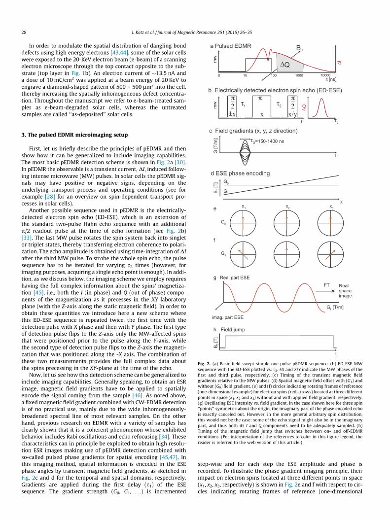
Fig. 2. (a) Basic field-swept simple one-pulse pEDMR sequence. (b) ED-ESE MWsequence with the ED-ESE plotted vs. s2. ±X and X/Y indicate the MW phases of thefirst and third pulse, respectively. (c) Timing of the transient magnetic fieldgradients relative to the MW pulses. (d) Spatial magnetic field offset with (G1) andwithout (G0) field gradient. (e) and (f) circles indicating rotating frames of reference(one-dimensional example) for electron spins (red arrows) located at three differentpoints in space (x1, x2 and x3) without and with applied field gradient, respectively.(g) Oscillating ESE intensity vs. field gradient. In the case shown here for three spin‘‘points’’ symmetric about the origin, the imaginary part of the phase encoded echois exactly canceled out. However, in the more general arbitrary spin distribution,this would not be the case: some of the echo signal might also be in the imaginarypart, and thus both its I and Q components need to be adequately sampled. (h)Timing of the magnetic field jump that switches between on- and off-EDMRconditions. (For interpretation of the references to color in this figure legend, thereader is referred to the web version of this article.)
3. The pulsed EDMR microimaging setup
First, let us briefly describe the principles of pEDMR and thenshow how it can be generalized to include imaging capabilities.The most basic pEDMR detection scheme is shown in Fig. 2a [30].In pEDMR the observable is a transient current, DI, induced follow-ing intense microwave (MW) pulses. In solar cells the pEDMR sig-nals may have positive or negative signs, depending on theunderlying transport process and operating conditions (see forexample [28] for an overview on spin-dependent transport pro-cesses in solar cells).
Another possible sequence used in pEDMR is the electrically-detected electron spin echo (ED-ESE), which is an extension ofthe standard two-pulse Hahn echo sequence with an additionalp/2 readout pulse at the time of echo formation (see Fig. 2b)[33]. The last MW pulse rotates the spin system back into singletor triplet states, thereby transferring electron coherence to polari-zation. The echo amplitude is obtained using time-integration of DIafter the third MW pulse. To strobe the whole spin echo, the pulsesequence has to be iterated for varying s2 times (however, forimaging purposes, acquiring a single echo point is enough). In addi-tion, as we discuss below, the imaging scheme we employ requireshaving the full complex information about the spins’ magnetiza-tion [45], i.e., both the I (in-phase) and Q (out-of-phase) compo-nents of the magnetization as it precesses in the XY laboratoryplane (with the Z-axis along the static magnetic field). In order toobtain these quantities we introduce here a new scheme wherethis ED-ESE sequence is repeated twice, the first time with thedetection pulse with X phase and then with Y phase. The first typeof detection pulse flips to the Z-axis only the MW-affected spinsthat were positioned prior to the pulse along the Y-axis, whilethe second type of detection pulse flips to the Z-axis the magneti-zation that was positioned along the -X axis. The combination ofthese two measurements provides the full complex data aboutthe spins precessing in the XY-plane at the time of the echo.
Now, let us see how this detection scheme can be generalized toinclude imaging capabilities. Generally speaking, to obtain an ESRimage, magnetic field gradients have to be applied to spatiallyencode the signal coming from the sample [46]. As noted above,a fixed magnetic field gradient combined with CW-EDMR detectionis of no practical use, mainly due to the wide inhomogenously-broadened spectral line of most relevant samples. On the otherhand, previous research on EDMR with a variety of samples hasclearly shown that it is a coherent phenomenon whose exhibitedbehavior includes Rabi oscillations and echo refocusing [34]. Thesecharacteristics can in principle be exploited to obtain high resolu-tion ESR images making use of pEDMR detection combined withso-called pulsed phase gradients for spatial encoding [45,47]. Inthis imaging method, spatial information is encoded in the ESEphase angles by transient magnetic field gradients, as sketched inFig. 2c and d for the temporal and spatial domains, respectively.Gradients are applied during the first delay (s1) of the ESEsequence. The gradient strength (G0, G1, . . .) is incremented
step-wise and for each step the ESE amplitude and phase isrecorded. To illustrate the phase gradient imaging principle, theirimpact on electron spins located at three different points in space(x1, x2, x3, respectively) is shown in Fig. 2e and f with respect to cir-cles indicating rotating frames of reference (one-dimensional

Fig. 3. Schematic block diagram of the pulsed EDMR imaging system (see also description in Ref. [49]). A computer (control PC) triggers MW pulses in the MW transceiver.These pulses go into the EDMR imaging probe, which is also fed by magnetic-field gradient pulses to spatially encode the sample, and by continuous light excitation to createcharge carries at cryogenic temperatures in the solar cell. The current in the solar cell is measured by a home-made differential current preamplifier and then goes into adiplexer (by mini-circuits) that feeds either the ‘‘I’’ or ‘‘Q’’ inputs of the digitizing card, depending on the phase of the third pulse in the imaging sequence (see also main text).
I. Katz et al. / Journal of Magnetic Resonance 251 (2015) 26–35 29
example). If no magnetic field gradient is applied (G0), all threeelectron spins remain stationary in the rotating frame (Fig. 2e).In the case of a finite gradient (Gi), electron spin j acquires a phaseangle uij ¼ cxj
RsG
Gidt, which results in I and Q components of theESE intensity of I �
Pj cos(uij) and Q�
Pj sin(uij) (Fig. 2f). Thus, in
the general case, as a result of the phase gradients the ESE intensityand phase will oscillate as a function of Gi. As depicted in Fig 2g, aFourier transform (FT) of this oscillating signal with respect to Gi
yields the real space distribution of the electron spins.The practical realization of such imaging scheme requires over-
coming some major experimental issues of concern. For example,pEDMR makes use of very sensitive current measurements of thesample under test. However, the MW pulses, especially the mag-netic field gradient pulses, create large transient currents alongthe wire leads. To cancel this disturbance, we implemented atwo-stage solution that includes both MW phase cycling and theapplication of a ‘‘field jump’’ protocol. Phase cycling is based on
a ± phase modulation of the first MW pulse in the sequence (seeFig. 2b) [48], which in turn modulates the phase of the echo signal.By repeating the sequence once with the +X phase and then withthe �X phase, and then subtracting the results, the current tran-sient is eliminated while the coherent EDMR echo signal that fol-lows the phase of the first pulse is reinforced. The ‘‘field jump’’protocol provides yet another mechanism for the reduction ofthe current transient (see Fig. 2h). Here again, the current mea-surement is repeated twice, once ‘‘on resonance’’ and then ‘‘off res-onance’’, by applying a fast current pulse through an auxiliary coilin the imaging probe that quickly (within a few microseconds)changes the resonance field. The unwanted current artifacts arethe same under both conditions and can thereby be eliminatedby subtracting ‘‘off resonance’’ from ‘‘on resonance’’ current tran-sients. Thus, by applying this two-stage solution (phase cyclingand field jump), spin-dependent and spin-independent electricalresponses may be separated from each other.
275 280 285 290 295
0
0.2
0.4
0.6
0.8
1
1.2
1.4
1.6
1.8
2
E D
- E S
E i n
t e n s
i t y
I [ n A
] Δ
E D
- E S
E i n
t e n s
i t y
I [ n A
] Δ
280 281 282 283 284 285 286 287 288 289 290
Magnetic field [mT]
-0.8
-0.7
-0.6
-0.5
-0.4
-0.3
-0.2
-0.1
0.1
0
Exp. datacbtvbt dbSimulation
Exp. datacbtvbt Simulation
10 K
100 K
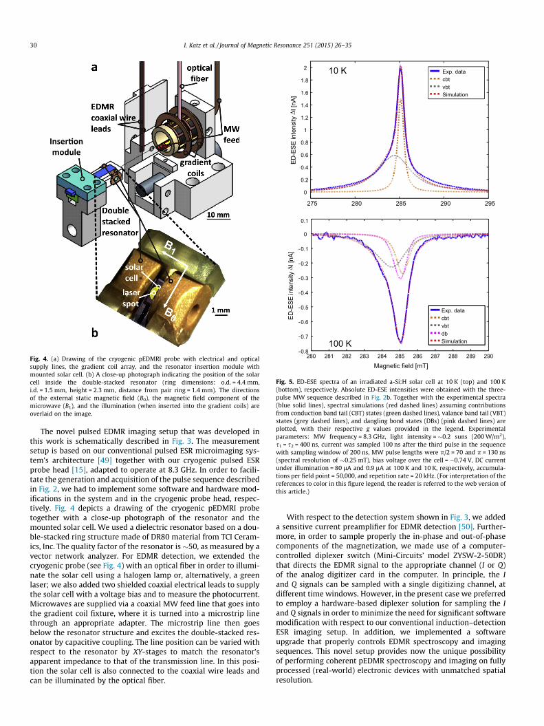
Fig. 5. ED-ESE spectra of an irradiated a-Si:H solar cell at 10 K (top) and 100 K(bottom), respectively. Absolute ED-ESE intensities were obtained with the three-pulse MW sequence described in Fig. 2b. Together with the experimental spectra(blue solid lines), spectral simulations (red dashed lines) assuming contributionsfrom conduction band tail (CBT) states (green dashed lines), valance band tail (VBT)states (grey dashed lines), and dangling bond states (DBs) (pink dashed lines) areplotted, with their respective g values provided in the legend. Experimentalparameters: MW frequency = 8.3 GHz, light intensity = �0.2 suns (200 W/m2),s1 = s2 = 400 ns, current was sampled 100 ns after the third pulse in the sequencewith sampling window of 200 ns, MW pulse lengths were p/2 = 70 and p = 130 ns(spectral resolution of �0.25 mT), bias voltage over the cell = �0.74 V, DC currentunder illumination = 80 lA and 0.9 lA at 100 K and 10 K, respectively, accumula-tions per field point = 50,000, and repetition rate = 20 kHz. (For interpretation of thereferences to color in this figure legend, the reader is referred to the web version ofthis article.)
Inser�on module
Fig. 4. (a) Drawing of the cryogenic pEDMRI probe with electrical and opticalsupply lines, the gradient coil array, and the resonator insertion module withmounted solar cell. (b) A close-up photograph indicating the position of the solarcell inside the double-stacked resonator (ring dimensions: o.d. = 4.4 mm,i.d. = 1.5 mm, height = 2.3 mm, distance from pair ring = 1.4 mm). The directionsof the external static magnetic field (B0), the magnetic field component of themicrowave (B1), and the illumination (when inserted into the gradient coils) areoverlaid on the image.
30 I. Katz et al. / Journal of Magnetic Resonance 251 (2015) 26–35
The novel pulsed EDMR imaging setup that was developed inthis work is schematically described in Fig. 3. The measurementsetup is based on our conventional pulsed ESR microimaging sys-tem’s architecture [49] together with our cryogenic pulsed ESRprobe head [15], adapted to operate at 8.3 GHz. In order to facili-tate the generation and acquisition of the pulse sequence describedin Fig. 2, we had to implement some software and hardware mod-ifications in the system and in the cryogenic probe head, respec-tively. Fig. 4 depicts a drawing of the cryogenic pEDMRI probetogether with a close-up photograph of the resonator and themounted solar cell. We used a dielectric resonator based on a dou-ble-stacked ring structure made of DR80 material from TCI Ceram-ics, Inc. The quality factor of the resonator is �50, as measured by avector network analyzer. For EDMR detection, we extended thecryogenic probe (see Fig. 4) with an optical fiber in order to illumi-nate the solar cell using a halogen lamp or, alternatively, a greenlaser; we also added two shielded coaxial electrical leads to supplythe solar cell with a voltage bias and to measure the photocurrent.Microwaves are supplied via a coaxial MW feed line that goes intothe gradient coil fixture, where it is turned into a microstrip linethrough an appropriate adapter. The microstrip line then goesbelow the resonator structure and excites the double-stacked res-onator by capacitive coupling. The line position can be varied withrespect to the resonator by XY-stages to match the resonator’sapparent impedance to that of the transmission line. In this posi-tion the solar cell is also connected to the coaxial wire leads andcan be illuminated by the optical fiber.
With respect to the detection system shown in Fig. 3, we addeda sensitive current preamplifier for EDMR detection [50]. Further-more, in order to sample properly the in-phase and out-of-phasecomponents of the magnetization, we made use of a computer-controlled diplexer switch (Mini-Circuits’ model ZYSW-2-50DR)that directs the EDMR signal to the appropriate channel (I or Q)of the analog digitizer card in the computer. In principle, the Iand Q signals can be sampled with a single digitizing channel, atdifferent time windows. However, in the present case we preferredto employ a hardware-based diplexer solution for sampling the Iand Q signals in order to minimize the need for significant softwaremodification with respect to our conventional induction–detectionESR imaging setup. In addition, we implemented a softwareupgrade that properly controls EDMR spectroscopy and imagingsequences. This novel setup provides now the unique possibilityof performing coherent pEDMR spectroscopy and imaging on fullyprocessed (real-world) electronic devices with unmatched spatialresolution.
a-Si:H solar cell EDMRI, T=10 K
TCO contact
Metalcontact
1 mm
Light spot
Solar cell
0.1
0.2
0.3
0.4
0.5
0.6
0.7
0.8
0.9
1
Degraded area
EDMRI, 10 K, degraded EDMRI, T=100 K, degraded
a b
c d
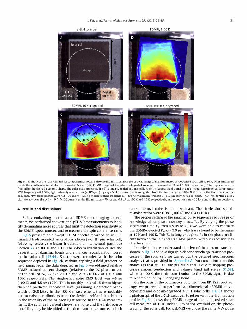
Fig. 6. (a) Photo of the solar cell and its components, showing also the illumination area. (b) pEDMR image of the illuminated as-deposited solar cell at 10 K, when measuredinside the double-stacked dielectric resonator. (c) and (d) pEDMR images of the e-beam-degraded solar cell, measured at 10 and 100 K, respectively. The degraded area isframed by the dashed diamond shape. The color code appearing in (d) is linearly scaled and normalized to the largest pixel signal in each image. Experimental parameters:MW frequency = 8.3 GHz, light intensity = �0.2 suns (200 W/m2), s1 = s2 = 500 ns, current was integrated from the time range of 100–8000 ns after the third pulse of thesequence, MW pulse lengths were p/2 = 60 and p = 120 ns, magnetic field gradients sG = 400 ns, maximum strength G = 6.5 T/m (for the X axis) and G = 4.3 T/m (for the Y axis),bias voltage over the cell = �0.74 V, DC current under illumination = 70 lA and 0.8 lA at 100 K and 10 K, respectively, and repetition rate = 20 kHz and 4 kHz, respectively.
I. Katz et al. / Journal of Magnetic Resonance 251 (2015) 26–35 31
4. Results and discussions
Before embarking on the actual EDMR microimaging experi-ments, we performed conventional pEDMR measurements to iden-tify dominating noise sources that limit the detection sensitivity ofthe EDMRI spectrometer, and to measure the spin coherence time.
Fig. 5 presents field-swept ED-ESE spectra recorded on an illu-minated hydrogenated amorphous silicon (a-Si:H) pin solar cell,following selective e-beam irradiation on its central part (seeSection 2), at 100 K and 10 K. The e-beam irradiation causes thegeneration of dangling bonds and enhances recombination lossesin the solar cell [43,44]. Spectra were recorded with the echosequence depicted in Fig. 2b, without applying a field gradient orfield jump. From the data depicted in Fig. 5 we obtained relativeEDMR-induced current changes (relative to the DC photocurrentof the cell) of DI/I � 9.25 � 10�6 and DI/I � 0.0022 at 100 K and10 K, respectively. The single-shot noise RMS level was �9 nA(100 K) and 4.5 nA (10 K). This is roughly �4 and 15 times higherthan the predicted shot-noise level (assuming a detection band-width of 200 kHz). In the 100-K measurement, this is probablydue to noise contributions from the device itself and instabilitiesin the intensity of the halogen light source. In the 10-K measure-ment, the solar cell current shows less noise and the light sourceinstability may be identified as the dominant noise source. In both
cases, thermal noise is not significant. The single-shot signal-to-noise ratios were 0.087 (100 K) and 0.43 (10 K).
The proper setting of the imaging pulse sequence requires priorknowledge about phase memory times, Tm. By varying the pulseseparation time s1 from 0.5 ls to 4 ls we were able to estimatethe EDMR-detected Tm as �3.6 ls, which was found to be the sameat 10 K and 100 K. This Tm is long enough to fit in the phase gradi-ents between the 90� and 180� MW pulses, without excessive lossof echo signal.
In order to better understand the sign of the current transientshown in Fig. 5 and to assign spin-dependent charge transport pro-cesses in the solar cell, we carried out the detailed spectroscopicanalysis that is provided in Appendix A. Our conclusion from thisanalysis is that at 10 K, the pEDMR signal is due to hopping pro-cesses among conduction and valance band tail states [51,52],while at 100 K, the main contribution to the EDMR signal is dueto recombination by Si dangling bonds.
On the basis of the parameters obtained from ED-ESE spectros-copy, we proceeded to perform two-dimensional pEDMRI on as-deposited and e-beam-degraded a-Si:H solar cells. Fig. 6a showsa photograph of the a-Si:H solar cell together with the illuminationprofile. Fig 6b shows the pEDMR image of the as-deposited solarcell measured at 10 K under illumination overlaid on the photo-graph of the solar cell. For pEDMRI we chose the same MW pulse
32 I. Katz et al. / Journal of Magnetic Resonance 251 (2015) 26–35
parameters as for ED-ESE spectroscopy. In addition, we applied400-ns-long magnetic field gradients and the field jump protocol,outlined in Fig. 2c and d. With these parameters and an accumula-tion time of �4 h, pEDMR images (100 � 64 pixels) were obtained.The pEDMR image depicted in Fig 6b is somewhat distorted due tonon-uniform gradient magnitudes (which in principle can be cor-rected by off-line image analysis). Nevertheless, the pixel resolu-tion of �22 � 34 lm clearly resolves the boundaries of the solarcell and the modulation of spin-dependent transport over the cell.This modulation is due to the excitation profile of the light source,which in our current setup does not illuminate the solar cell uni-formly. The spatial distribution of the spin-dependent transportsignal over the cell may be rationalized by the underlying pro-cesses. First, higher light intensity results in a larger photocurrentand therefore a larger overall measured DI. Second, at 10 K andwith an applied bias, the pEDMR signal is dominated by spin-dependent hopping via conduction band tail (CBT) and valenceband tail (VBT) states. With increasing light intensity, the quasi-Fermi level of holes and electrons is pushed closer to the edgesof the conduction and valence band, and hence into regions witha higher density of states. This results in a decrease in averagehop times, which enhances the EDMR signal’s intensity, DI/I.
Subsequently, we carried out pEDMRI on a solar cell that wassubjected to e-beam degradation within a 500 lm � 500 lm dia-mond-shaped region (see Section 2). Fig. 6c and d depict pEDMRimages obtained from the irradiated cell at 10 K and 100 K, respec-tively. Except for the number of pixels (64 � 40 at 100 K and80 � 60 at 10 K), these images were acquired with the same exper-imental parameters as Fig. 6b.
When comparing 10-K pEDMR images obtained on as-depos-ited (Fig. 6b) and e-beam-degraded (Fig. 6c) solar cells, spin-dependent current patterns may be identified. In both cases, thestrength of the spin-dependent hopping signal depends on theexcitation profile of the light source. However, the e-beam-degraded cell shows also a pronounced decrease of the spin-dependent current as compared to the as-deposited cell. This inter-esting finding is not fully understood yet. Possible reasons could bean increase of non-spin-dependent recombination pathways viadoubly-occupied dangling bonds [52], or a reduction of the averagehop time due to the shift of the a-Si:H quasi-Fermi levels towardsmidgap where defects can be generated by the e-beam exposure[53].
Upon increasing the temperature, the pEDMR image of the solarcell changes again dramatically (see Fig. 6d). At 100 K, the e-beam-irradiated region exhibits a strongly increased EDMR signal ascompared to the surrounding parts of the solar cell. This is inagreement with many observations showing that e-beam-irradia-tion increases the number of dangling bonds and leads to increasedspin-dependent trapping and recombination (revealed herethrough local spatially-resolved data). This also supports the EDMRspectroscopy data in Appendix A which showed that the 100-KEDMR signal originates from recombination involving CBT statesand DBs. This reduction of the lifetime is manifested in an increasein EDMR signal intensity.
These first high resolution functional in-operando pEDMRimages on real-world solar cells demonstrate the potential of thisnovel technique to locate spin-dependent transport and loss mech-anisms in an electronic device, and reveal the spatial distributionof function-determining paramagnetic states in fully processedelectronic devices.
5. Conclusions and future prospects
The basic approach to pulsed EDMR imaging by pulsed phasegradients has proven to work well. Nevertheless, there is still
plenty of room for improvement. The fundamental limiting factorin our pEDMR imaging experiment is the signal-to-noise ratio(SNR). Our phase gradient drivers can provide much more powerfulgradients than the ones used in this experiment, and currently sup-port resolutions down to 80 nm [49,54]. However, at such resolu-tion the noise level in our experiment will be too high, since thenumber of defects, or states, in a given voxel will be too small toobserve. Improvements in SNR can be achieved, first of all, by usinga more stable light source that does not have significant noise com-ponents at the �1–500 kHz range. This can increase SNR by a factorof �4 by reaching the shot-noise limit. Furthermore, increasing thelight intensity to at least 3.2 suns would lead to �16 times morecurrent than obtained here, meaning an increase in SNR by a factorof 4. Additional significant improvements can be gained by usingsmaller cells with a smaller overall shot noise (e.g., a cell with asize of �10 � 10 lm would lead to a hundredfold improvementin SNR).
The cumulative effect of these near-future improvements canincrease SNR by a factor of �1600, meaning that it is possible toreach an image resolution in the scale of a few hundreds of nano-meters for the type of cells we employed here. We can estimate theconcentration of the defect states that contribute to the spin-dependent current component in this material to be �1016 statesper cm3 [55]. This means that Fig. 6b shows �107 states in eachvoxel in the EDMR image, with an SNR of �200. Clearly, it wouldnot have been possible to obtain such sensitivity (and conse-quently, image resolution) with such sample and spin propertiesusing conventional ESR. Other solar cells or semiconductor devicesthat have paramagnetic species or states with larger concentra-tions may make it possible to reach even higher spatial resolutionsin the nanometer scale. For example, since an EDMR signal for P-doped Si can be obtained for less than 100 spins, it follows that a3D resolution of �100 nm should be readily available with suchtype of sample having a P concentration of �1016 atoms/cm3.
The method developed here can be widely used for the nonde-structive inspection of paramagnetic species in a variety of solid-state electronic devices, especially in the emerging field of nano-structured or nanocomposite 3D semiconductor devices. Althoughthe experimental results presented here have limited resolution,relatively simple future improvements will greatly enhance thecapabilities of the pulsed EDMRI experiment, resulting in resolu-tions on the scale of hundreds of nanometers. It should also benoted that our setup can support also 3D and 4D imaging capabil-ities (with the 4th dimension referring to the EDMR spectrum).
It is worth mentioning that the presented EDMRI technique hasa potential for defect characterization on electronic devices thatgoes beyond imaging of spin-dependent electronic transport, byproviding images of the total current of the device. Many deviceswould normally have a homogenous spin-dependent EDMR cur-rent signature, meaning that DI/I should be the same for the entiredevice. However, EDMR imaging of such devices may still revealsome significant heterogeneity, which in such cases may resultonly from local changes in the overall current. The latter whichmay be quenched or enhanced in the device due to defects unre-lated to spins or spin-dependent processes, such as crystaldislocations.
Acknowledgments
This work was partially supported by Grant #G-1032-18.14/2009 from the German–Israeli Foundation (GIF), Grant #213/09from the Israeli Science Foundation, Grants #201665 and#309649 from the European Research Council (ERC), and by theRussell Berrie Nanotechnology Institute at the Technion. MFreceived funding from the German Research Foundation withinSPP 1601. We thank F. Finger and O, Astakhov (Forschungszentrum
344338 342340 346Magne�c field [mT] Temperature [K]
10050 150 200 250 300
Sign
al [a
.u.]
00
20
40
a b
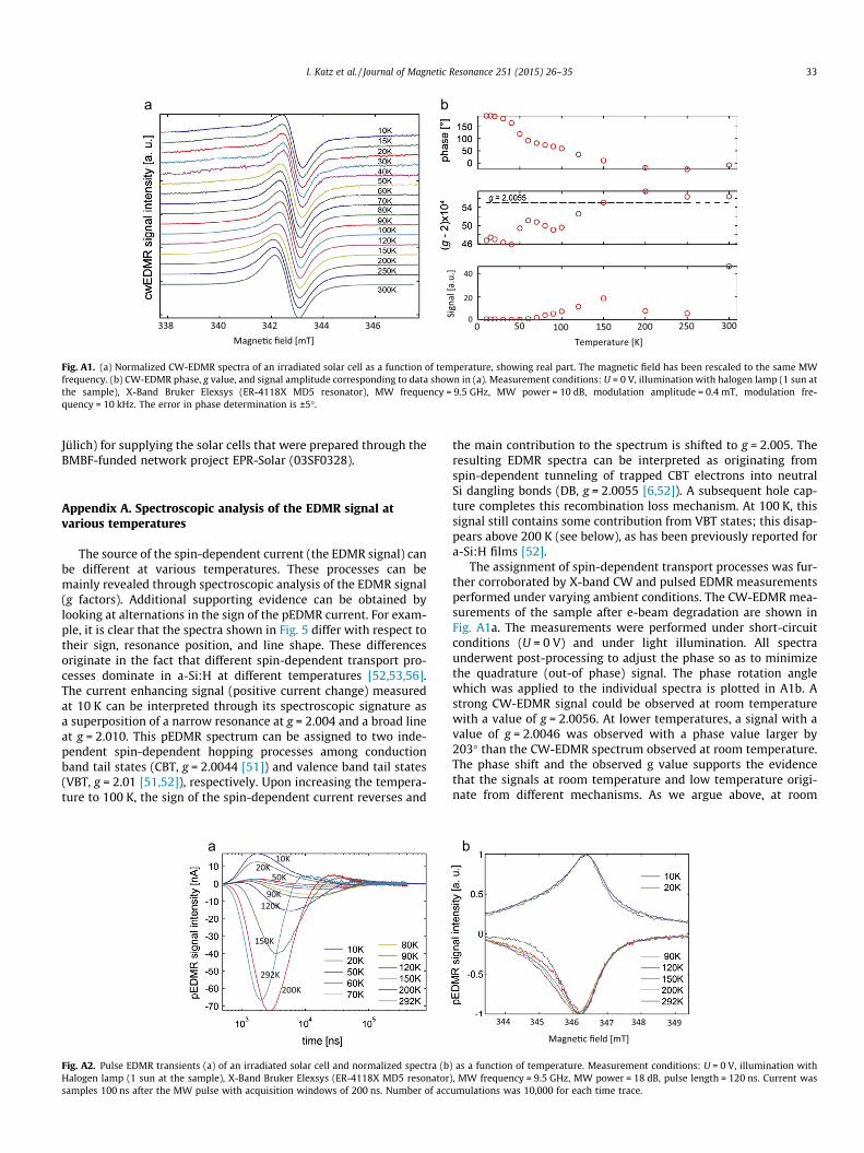
Fig. A1. (a) Normalized CW-EDMR spectra of an irradiated solar cell as a function of temperature, showing real part. The magnetic field has been rescaled to the same MWfrequency. (b) CW-EDMR phase, g value, and signal amplitude corresponding to data shown in (a). Measurement conditions: U = 0 V, illumination with halogen lamp (1 sun atthe sample), X-Band Bruker Elexsys (ER-4118X MD5 resonator), MW frequency = 9.5 GHz, MW power = 10 dB, modulation amplitude = 0.4 mT, modulation fre-quency = 10 kHz. The error in phase determination is ±5�.
I. Katz et al. / Journal of Magnetic Resonance 251 (2015) 26–35 33
Jülich) for supplying the solar cells that were prepared through theBMBF-funded network project EPR-Solar (03SF0328).
Appendix A. Spectroscopic analysis of the EDMR signal atvarious temperatures
The source of the spin-dependent current (the EDMR signal) canbe different at various temperatures. These processes can bemainly revealed through spectroscopic analysis of the EDMR signal(g factors). Additional supporting evidence can be obtained bylooking at alternations in the sign of the pEDMR current. For exam-ple, it is clear that the spectra shown in Fig. 5 differ with respect totheir sign, resonance position, and line shape. These differencesoriginate in the fact that different spin-dependent transport pro-cesses dominate in a-Si:H at different temperatures [52,53,56].The current enhancing signal (positive current change) measuredat 10 K can be interpreted through its spectroscopic signature asa superposition of a narrow resonance at g = 2.004 and a broad lineat g = 2.010. This pEDMR spectrum can be assigned to two inde-pendent spin-dependent hopping processes among conductionband tail states (CBT, g = 2.0044 [51]) and valence band tail states(VBT, g = 2.01 [51,52]), respectively. Upon increasing the tempera-ture to 100 K, the sign of the spin-dependent current reverses and
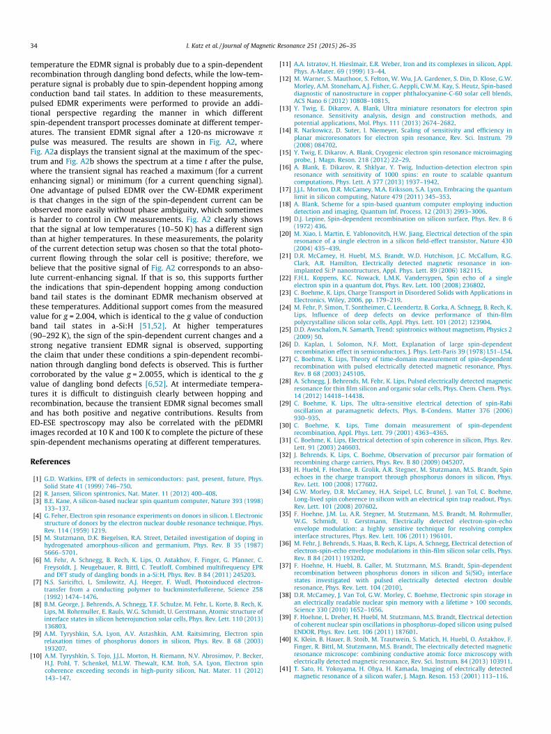
10K 20K
200K
292K
150K
120K 90K
50K
a
Fig. A2. Pulse EDMR transients (a) of an irradiated solar cell and normalized spectra (bHalogen lamp (1 sun at the sample), X-Band Bruker Elexsys (ER-4118X MD5 resonatorsamples 100 ns after the MW pulse with acquisition windows of 200 ns. Number of acc
the main contribution to the spectrum is shifted to g = 2.005. Theresulting EDMR spectra can be interpreted as originating fromspin-dependent tunneling of trapped CBT electrons into neutralSi dangling bonds (DB, g = 2.0055 [6,52]). A subsequent hole cap-ture completes this recombination loss mechanism. At 100 K, thissignal still contains some contribution from VBT states; this disap-pears above 200 K (see below), as has been previously reported fora-Si:H films [52].
The assignment of spin-dependent transport processes was fur-ther corroborated by X-band CW and pulsed EDMR measurementsperformed under varying ambient conditions. The CW-EDMR mea-surements of the sample after e-beam degradation are shown inFig. A1a. The measurements were performed under short-circuitconditions (U = 0 V) and under light illumination. All spectraunderwent post-processing to adjust the phase so as to minimizethe quadrature (out-of phase) signal. The phase rotation anglewhich was applied to the individual spectra is plotted in A1b. Astrong CW-EDMR signal could be observed at room temperaturewith a value of g = 2.0056. At lower temperatures, a signal with avalue of g = 2.0046 was observed with a phase value larger by203� than the CW-EDMR spectrum observed at room temperature.The phase shift and the observed g value supports the evidencethat the signals at room temperature and low temperature origi-nate from different mechanisms. As we argue above, at room
344 345 346 347 348 349
Magne�c field [mT]
b
) as a function of temperature. Measurement conditions: U = 0 V, illumination with), MW frequency = 9.5 GHz, MW power = 18 dB, pulse length = 120 ns. Current wasumulations was 10,000 for each time trace.
34 I. Katz et al. / Journal of Magnetic Resonance 251 (2015) 26–35
temperature the EDMR signal is probably due to a spin-dependentrecombination through dangling bond defects, while the low-tem-perature signal is probably due to spin-dependent hopping amongconduction band tail states. In addition to these measurements,pulsed EDMR experiments were performed to provide an addi-tional perspective regarding the manner in which differentspin-dependent transport processes dominate at different temper-atures. The transient EDMR signal after a 120-ns microwave ppulse was measured. The results are shown in Fig. A2, whereFig. A2a displays the transient signal at the maximum of the spec-trum and Fig. A2b shows the spectrum at a time t after the pulse,where the transient signal has reached a maximum (for a currentenhancing signal) or minimum (for a current quenching signal).One advantage of pulsed EDMR over the CW-EDMR experimentis that changes in the sign of the spin-dependent current can beobserved more easily without phase ambiguity, which sometimesis harder to control in CW measurements. Fig. A2 clearly showsthat the signal at low temperatures (10–50 K) has a different signthan at higher temperatures. In these measurements, the polarityof the current detection setup was chosen so that the total photo-current flowing through the solar cell is positive; therefore, webelieve that the positive signal of Fig. A2 corresponds to an abso-lute current-enhancing signal. If that is so, this supports furtherthe indications that spin-dependent hopping among conductionband tail states is the dominant EDMR mechanism observed atthese temperatures. Additional support comes from the measuredvalue for g = 2.004, which is identical to the g value of conductionband tail states in a-Si:H [51,52]. At higher temperatures(90–292 K), the sign of the spin-dependent current changes and astrong negative transient EDMR signal is observed, supportingthe claim that under these conditions a spin-dependent recombi-nation through dangling bond defects is observed. This is furthercorroborated by the value g = 2.0055, which is identical to the gvalue of dangling bond defects [6,52]. At intermediate tempera-tures it is difficult to distinguish clearly between hopping andrecombination, because the transient EDMR signal becomes smalland has both positive and negative contributions. Results fromED-ESE spectroscopy may also be correlated with the pEDMRIimages recorded at 10 K and 100 K to complete the picture of thesespin-dependent mechanisms operating at different temperatures.
References
[1] G.D. Watkins, EPR of defects in semiconductors: past, present, future, Phys.Solid State 41 (1999) 746–750.
[2] R. Jansen, Silicon spintronics, Nat. Mater. 11 (2012) 400–408.[3] B.E. Kane, A silicon-based nuclear spin quantum computer, Nature 393 (1998)
133–137.[4] G. Feher, Electron spin resonance experiments on donors in silicon. I. Electronic
structure of donors by the electron nuclear double resonance technique, Phys.Rev. 114 (1959) 1219.
[5] M. Stutzmann, D.K. Biegelsen, R.A. Street, Detailed investigation of doping inhydrogenated amorphous-silicon and germanium, Phys. Rev. B 35 (1987)5666–5701.
[6] M. Fehr, A. Schnegg, B. Rech, K. Lips, O. Astakhov, F. Finger, G. Pfanner, C.Freysoldt, J. Neugebauer, R. Bittl, C. Teutloff, Combined multifrequency EPRand DFT study of dangling bonds in a-Si:H, Phys. Rev. B 84 (2011) 245203.
[7] N.S. Sariciftci, L. Smilowitz, A.J. Heeger, F. Wudl, Photoinduced electron-transfer from a conducting polymer to buckminsterfullerene, Science 258(1992) 1474–1476.
[8] B.M. George, J. Behrends, A. Schnegg, T.F. Schulze, M. Fehr, L. Korte, B. Rech, K.Lips, M. Rohrmuller, E. Rauls, W.G. Schmidt, U. Gerstmann, Atomic structure ofinterface states in silicon heterojunction solar cells, Phys. Rev. Lett. 110 (2013)136803.
[9] A.M. Tyryshkin, S.A. Lyon, A.V. Astashkin, A.M. Raitsimring, Electron spinrelaxation times of phosphorus donors in silicon, Phys. Rev. B 68 (2003)193207.
[10] A.M. Tyryshkin, S. Tojo, J.J.L. Morton, H. Riemann, N.V. Abrosimov, P. Becker,H.J. Pohl, T. Schenkel, M.L.W. Thewalt, K.M. Itoh, S.A. Lyon, Electron spincoherence exceeding seconds in high-purity silicon, Nat. Mater. 11 (2012)143–147.
[11] A.A. Istratov, H. Hieslmair, E.R. Weber, Iron and its complexes in silicon, Appl.Phys. A-Mater. 69 (1999) 13–44.
[12] M. Warner, S. Mauthoor, S. Felton, W. Wu, J.A. Gardener, S. Din, D. Klose, G.W.Morley, A.M. Stoneham, A.J. Fisher, G. Aeppli, C.W.M. Kay, S. Heutz, Spin-baseddiagnostic of nanostructure in copper phthalocyanine-C-60 solar cell blends,ACS Nano 6 (2012) 10808–10815.
[13] Y. Twig, E. Dikarov, A. Blank, Ultra miniature resonators for electron spinresonance. Sensitivity analysis, design and construction methods, andpotential applications, Mol. Phys. 111 (2013) 2674–2682.
[14] R. Narkowicz, D. Suter, I. Niemeyer, Scaling of sensitivity and efficiency inplanar microresonators for electron spin resonance, Rev. Sci. Instrum. 79(2008) 084702.
[15] Y. Twig, E. Dikarov, A. Blank, Cryogenic electron spin resonance microimagingprobe, J. Magn. Reson. 218 (2012) 22–29.
[16] A. Blank, E. Dikarov, R. Shklyar, Y. Twig, Induction-detection electron spinresonance with sensitivity of 1000 spins: en route to scalable quantumcomputations, Phys. Lett. A 377 (2013) 1937–1942.
[17] J.J.L. Morton, D.R. McCamey, M.A. Eriksson, S.A. Lyon, Embracing the quantumlimit in silicon computing, Nature 479 (2011) 345–353.
[18] A. Blank, Scheme for a spin-based quantum computer employing inductiondetection and imaging, Quantum Inf. Process. 12 (2013) 2993–3006.
[19] D.J. Lepine, Spin-dependent recombination on silicon surface, Phys. Rev. B 6(1972) 436.
[20] M. Xiao, I. Martin, E. Yablonovitch, H.W. Jiang, Electrical detection of the spinresonance of a single electron in a silicon field-effect transistor, Nature 430(2004) 435–439.
[21] D.R. McCamey, H. Huebl, M.S. Brandt, W.D. Hutchison, J.C. McCallum, R.G.Clark, A.R. Hamilton, Electrically detected magnetic resonance in ion-implanted Si:P nanostructures, Appl. Phys. Lett. 89 (2006) 182115.
[22] F.H.L. Koppens, K.C. Nowack, L.M.K. Vandersypen, Spin echo of a singleelectron spin in a quantum dot, Phys. Rev. Lett. 100 (2008) 236802.
[23] C. Boehme, K. Lips, Charge Transport in Disordered Solids with Applications inElectronics, Wiley, 2006, pp. 179–219.
[24] M. Fehr, P. Simon, T. Sontheimer, C. Leendertz, B. Gorka, A. Schnegg, B. Rech, K.Lips, Influence of deep defects on device performance of thin-filmpolycrystalline silicon solar cells, Appl. Phys. Lett. 101 (2012) 123904.
[25] D.D. Awschalom, N. Samarth, Trend: spintronics without magnetism, Physics 2(2009) 50.
[26] D. Kaplan, I. Solomon, N.F. Mott, Explanation of large spin-dependentrecombination effect in semiconductors, J. Phys. Lett-Paris 39 (1978) L51–L54.
[27] C. Boehme, K. Lips, Theory of time-domain measurement of spin-dependentrecombination with pulsed electrically detected magnetic resonance, Phys.Rev. B 68 (2003) 245105.
[28] A. Schnegg, J. Behrends, M. Fehr, K. Lips, Pulsed electrically detected magneticresonance for thin film silicon and organic solar cells, Phys. Chem. Chem. Phys.14 (2012) 14418–14438.
[29] C. Boehme, K. Lips, The ultra-sensitive electrical detection of spin-Rabioscillation at paramagnetic defects, Phys. B-Condens. Matter 376 (2006)930–935.
[30] C. Boehme, K. Lips, Time domain measurement of spin-dependentrecombination, Appl. Phys. Lett. 79 (2001) 4363–4365.
[31] C. Boehme, K. Lips, Electrical detection of spin coherence in silicon, Phys. Rev.Lett. 91 (2003) 246603.
[32] J. Behrends, K. Lips, C. Boehme, Observation of precursor pair formation ofrecombining charge carriers, Phys. Rev. B 80 (2009) 045207.
[33] H. Huebl, F. Hoehne, B. Grolik, A.R. Stegner, M. Stutzmann, M.S. Brandt, Spinechoes in the charge transport through phosphorus donors in silicon, Phys.Rev. Lett. 100 (2008) 177602.
[34] G.W. Morley, D.R. McCamey, H.A. Seipel, L.C. Brunel, J. van Tol, C. Boehme,Long-lived spin coherence in silicon with an electrical spin trap readout, Phys.Rev. Lett. 101 (2008) 207602.
[35] F. Hoehne, J.M. Lu, A.R. Stegner, M. Stutzmann, M.S. Brandt, M. Rohrmuller,W.G. Schmidt, U. Gerstmann, Electrically detected electron-spin-echoenvelope modulation: a highly sensitive technique for resolving complexinterface structures, Phys. Rev. Lett. 106 (2011) 196101.
[36] M. Fehr, J. Behrends, S. Haas, B. Rech, K. Lips, A. Schnegg, Electrical detection ofelectron-spin-echo envelope modulations in thin-film silicon solar cells, Phys.Rev. B 84 (2011) 193202.
[37] F. Hoehne, H. Huebl, B. Galler, M. Stutzmann, M.S. Brandt, Spin-dependentrecombination between phosphorus donors in silicon and Si/SiO2 interfacestates investigated with pulsed electrically detected electron doubleresonance, Phys. Rev. Lett. 104 (2010).
[38] D.R. McCamey, J. Van Tol, G.W. Morley, C. Boehme, Electronic spin storage inan electrically readable nuclear spin memory with a lifetime > 100 seconds,Science 330 (2010) 1652–1656.
[39] F. Hoehne, L. Dreher, H. Huebl, M. Stutzmann, M.S. Brandt, Electrical detectionof coherent nuclear spin oscillations in phosphorus-doped silicon using pulsedENDOR, Phys. Rev. Lett. 106 (2011) 187601.
[40] K. Klein, B. Hauer, B. Stoib, M. Trautwein, S. Matich, H. Huebl, O. Astakhov, F.Finger, R. Bittl, M. Stutzmann, M.S. Brandt, The electrically detected magneticresonance microscope: combining conductive atomic force microscopy withelectrically detected magnetic resonance, Rev. Sci. Instrum. 84 (2013) 103911.
[41] T. Sato, H. Yokoyama, H. Ohya, H. Kamada, Imaging of electrically detectedmagnetic resonance of a silicon wafer, J. Magn. Reson. 153 (2001) 113–116.

I. Katz et al. / Journal of Magnetic Resonance 251 (2015) 26–35 35
[42] Y. Mai, S. Klein, R. Carius, H. Stiebig, X. Geng, F. Finger, Open circuit voltageimprovement of high-deposition-rate microcrystalline silicon solar cells byhot wire interface layers, Appl. Phys. Lett. 87 (2005) 073503.
[43] U. Schneider, B. Schroder, F. Finger, Saturation effect and annealing behavior ofmetastable defects induced by Kev – electron-irradiation in intrinsic a-Si-H, J.Non-Cryst. Solids 114 (1989) 633–635.
[44] O. Astakhov, R. Carius, F. Finger, Y. Petrusenko, V. Borysenko, D. Barankov,Relationship between defect density and charge carrier transport inamorphous and microcrystalline silicon, Phys. Rev. B 79 (2009) 104205.
[45] A. Coy, N. Kaplan, P.T. Callaghan, Three-dimensional pulsed ESR imaging, J.Magn. Reson. Ser. A 121 (1996) 201–205.
[46] P.T. Callaghan, Principles of Nuclear Magnetic Resonance Microscopy, OxfordUniversity Press, Oxford, 1991.
[47] A. Blank, C.R. Dunnam, P.P. Borbat, J.H. Freed, Pulsed three-dimensionalelectron spin resonance microscopy, Appl. Phys. Lett. 85 (2004) 5430–5432.
[48] F. Hoehne, L. Dreher, J. Behrends, M. Fehr, H. Huebl, K. Lips, A. Schnegg, M.Suckert, M. Stutzmann, M.S. Brandt, Lock-in detection for pulsed electricallydetected magnetic resonance, Rev. Sci. Instrum. 83 (2012) 043907.
[49] L. Shtirberg, Y. Twig, E. Dikarov, R. Halevy, M. Levit, A. Blank, High-sensitivityQ-band electron spin resonance imaging system with submicron resolution,Rev. Sci. Instrum. 82 (2011) 043708.
[50] J. Behrends, A. Schnegg, M. Fehr, A. Lambertz, S. Haas, F. Finger, B. Rech, K. Lips,Electrical detection of electron spin resonance in microcrystalline silicon pinsolar cells, Philos. Mag. 89 (2009) 2655–2676.
[51] T. Umeda, S. Yamasaki, J. Isoya, K. Tanaka, Microscopic origin of light-inducedESR centers in undoped hydrogenated amorphous silicon, Phys. Rev. B 62(2000) 15702–15710.
[52] H. Dersch, L. Schweitzer, J. Stuke, Recombination processes in a-Si-H – spin-dependent photoconductivity, Phys. Rev. B 28 (1983) 4678–4684.
[53] K. Lips, S. Schutte, W. Fuhs, Microwave-induced resonant changes in transportand recombination in hydrogenated amorphous-silicon, Philos. Mag. B 65(1992) 945–959.
[54] L. Shtirberg, A. Blank, Short, powerful, and agile current drivers for magneticresonance, Concept Magn. Reson. B 39B (2011) 119–127.
[55] T. Umeda, S. Yamasaki, J. Isoya, A. Matsuda, K. Tanaka, Energy location of light-induced ESR centers in undoped a-Si:H, J. Non-Cryst. Solids 227 (1998) 353–357.
[56] M.S. Brandt, M. Stutzmann, Spin-dependent conductivity in amorphoushydrogenated silicon, Phys. Rev. B 43 (1991) 5184–5187.