journal of nanomedicine & nanotechnology · pdf filecitation: md asgar a, hasan m, md huq...
TRANSCRIPT
Research Article Open Access
Md Asgar et al., J Nanomed Nanotechnol 2014, 5:4 DOI: 10.4172/2157-7439.1000221
Volume 5 • Issue 4 • 1000221J Nanomed NanotechnolISSN: 2157-7439 JNMNT, an open access journal
Keywords: Silicon nanowires; Scanning electron microscopy;Carbon nanotubes; Nanostructure arrays
IntroductionResearch attention in semiconducting nanostructures has been
decoupled after successful synthesis of Carbon Nano-Tubes (CNTs), for their novel size and dimensionality dependent physical properties [1,2]. To date, the most significant semiconducting material in microelectronic industries is silicon (Si), owing to their technical compatibility with existing semiconductor technology. Though silicon cannot emit visible light as being an indirect material, low dimensional Si nanostructures yield visible light because of quantum confinement effect [3-5]. As a result, much effort has been made to prepare various silicon nanostructures such as Silicon nanotubes, Silicon Nano-Cones (SiNCs) and Silicon Nano-Wires (SiNWs) etc [6-9].
Silicon nanowires (SiNWs) have recently been the subject of great scientific and technological interest by reason of their noble electrical [10] optoelectronic [11], mechanical [12] and chemical properties [13]. Several promising application of Si nanowires array are found in different microelectronic industries, for instance, Field-Effect Transistors (FETs) [14,15], Single-Electron Transistors (SETs) [16], inverters [17], photovoltaics and photodetectors [18], nanosensors [19,20], Light-Emitting Diodes (LEDs) and laser [14-21], decoder [22],
nonvolatile memory, programmable logic [23-25] and silicon nano-anodes in practical lithium batteries [26] etc.
Many other applications have been verified primarily in the form of individual nanowire devices, though some devices based on arrays have also been shown [27]. One feature that has been generally overlooked is the interaction of light of varying wavelength with nanowire assemblies on p-type Si substrate, which may have implications for future optical and optoelectronic devices such as Laser, optical sensor [28]. and nano-photovoltaic solar cell [29]. The high aspect ratio of nanowires (typically on the order of 100 to 1000) and sharp dielectric contrast with its surrounding (e.g. air or glass) lead to optical anisotropy as observed in individual silicon nanowires [30]. Moreover, sub-wavelength diameters and proximity, combined with micron-scale lengths, may lead to interesting optical properties such as low reflectance through better
*Corresponding author: Md Huq F, Department of Nuclear Engineering,University of Dhaka, Dhaka 1000, Bangladesh, Tel: 8801913377384; E-mail:[email protected]
Received April 26, 2014; Accepted August 20, 2014; Published August 27, 2014
Citation: Md Asgar A, Hasan M, Md Huq F, Mahmood ZH (2014) Metal AssistedSynthesis of Single Crystalline Silicon Nanowires at Room Temperature forPhotovoltaic Application. J Nanomed Nanotechnol 5: 221. doi: 10.4172/2157-7439.1000221
Copyright: © 2014 Md Asgar A, et al. This is an open-access article distributed under the terms of the Creative Commons Attribution License, which permits unrestricted use, distribution, and reproduction in any medium, provided the original author and source are credited.
Metal Assisted Synthesis of Single Crystalline Silicon Nanowires at Room Temperature for Photovoltaic ApplicationMd Asgar A1, Hasan M2, Md Huq F3* and Zahid H Mahmood4
1Department of Electronics and Communication Engineering, Jatiya Kabi Kazi Nazrul Islam University, Trishal, Mymensingh, Bangladesh2Department of Electrical and Electronic Engineering, Shahjalal University of Science and Technology, Kumargaon, Sylhet-3114, Bangladesh3Department of Nuclear Engineering, University of Dhaka, Dhaka 1000, Bangladesh4Department of Applied Physics Electronics and Communication Engineering, University of Dhaka, Dhaka-1000, Bangladesh
AbstractSynthesis of single crystalline silicon nanowires (SiNWs) array at room temperature by metal assisted chemical
etching and its optical absorption measurements have been reported in this article. It has been confirmed that, SiNWs were formed uniformly on p-type silicon substrate by electroless deposition of Cu and Ag nanoparticles followed by wet chemical etching in (Hydrogen Fluoride) HF based Fe(NO3)3 solution. Synthesized SiNW structures were analyzed and investigated by Scanning Electron Microscopy (SEM) and Ultraviolet-Visible (UV-VIS) spectrophotometer. Formation of SiNWs is evident from the SEM images and morphology of the structures depends upon the concentration of chemical solution and etching time. The synthesized SiNWs have shown strong broadband optical absorption exhibited from UV-spectroscopy. More than 82% absorption of incident radiation is found for Cu treated samples and a maximum of 83% absorption of incident radiation is measured for Ag synthesized samples which is considerably enhanced than that of silicon substrate as they absorbed maximum of 43% of incoming radiation only.
light trapping and as we have shown in this paper, high absorption [31,32].
Herein, we have reported the room-temperature synthesis of highly oriented SiNWs array, using simple chemical technique named Electroless Metal Deposition (EMD) and metal-assisted Electroless Etching (EE) of Si wafers in an aqueous HF solution containing Fe3+ ions. We have employed this method because it has several advantages over many other established methods. This technique is cost effective and functions without requiring any vacuum and high temperature requirement. Growth of SiNWs by this technique is slightly depends on the crystallographic orientation which makes them to utilize polycrystalline substrate [33]. This chemical electrolytic process is based on a galvanic displacement reaction. In this method oxidization of metal ions to metallic species such as particles and films, and the dissolution of silicon substrate occur extemporaneously on a silicon surface.
After successful synthesis of Silicon nanowires (SiNWs) we have investigated the optical behaviour of synthesized structures by means of Ultraviolet-Visible (UV-VIS) spectroscopy. Silicon nanowire (SiNW) arrays synthesized by wet-chemical etching process have revealed very high absorption for a particular range of wavelength of electromagnetic spectrum. This high broadband optical absorption of SiNWs array makes them an important contestant for photovoltaic solar cell applications.
Journal ofNanomedicine & NanotechnologyJo
urna
l of N
anomedicine & Nanotechnology
ISSN: 2157-7439
Citation: Md Asgar A, Hasan M, Md Huq F, Mahmood ZH (2014) Metal Assisted Synthesis of Single Crystalline Silicon Nanowires at Room Temperature for Photovoltaic Application. J Nanomed Nanotechnol 5: 221. doi: 10.4172/2157-7439.1000221
Page 2 of 7
Volume 5 • Issue 4 • 1000221J Nanomed NanotechnolISSN: 2157-7439 JNMNT, an open access journal
Experimental DetailsPreparation of 1D silicon nanostructures array was conducted in
Teflon lined stainless steel vessel. The fabrication process comprised of three steps. The first step is cleaning of the silicon wafers with cleaning solution— here we sequentially used acetone (5 min), ethanol (5 min), deionized water (2-3 times), and H2SO4/H2O2 (3:1 H2SO4 (97%)/ H2O2 (30%), 10 min), then the wafers are thoroughly rinsed with deionized water (10 min) and dip into a solution of HF (1 min). The second step of fabrication is electroplating the metal-nanoparticle films onto the cleaned silicon surface. A group of cleaned samples were dipped in HF/AgNO3 solution for Silver nanoparticle deposition. Deposition time was varied from 60 seconds to 75 seconds. The concentration of HF and AgNO3 were 5 M and 0.02 M respectively. Another group of samples were dipped in HF/Cu(NO3)2.H2O for copper nanoparticles deposition. In this case, deposition time was varied from 60 seconds to 120 seconds. The concentration of HF was 5 M, whereas for Cu(NO3)2.H2O, it was varied from 0.02 M to 0.05 M. All the above mentioned chemical processes performed in Teflon beaker. After deposition of silver/copper nanoparticles, the silver/copper deposited substrate was immersed in another solution for etching of uncovered areas of the silicon substrate. The solution was HF based Fe(NO3)3, where the concentration of HF and Fe(NO3)3 were 5 M and 0.02 M respectively. Etching was performed at room temperature and etching time was varied from 30 min to 120 min for different samples. After the preparation process, the obtained samples were rinsed copiously in deionized water and dried at room temperature.
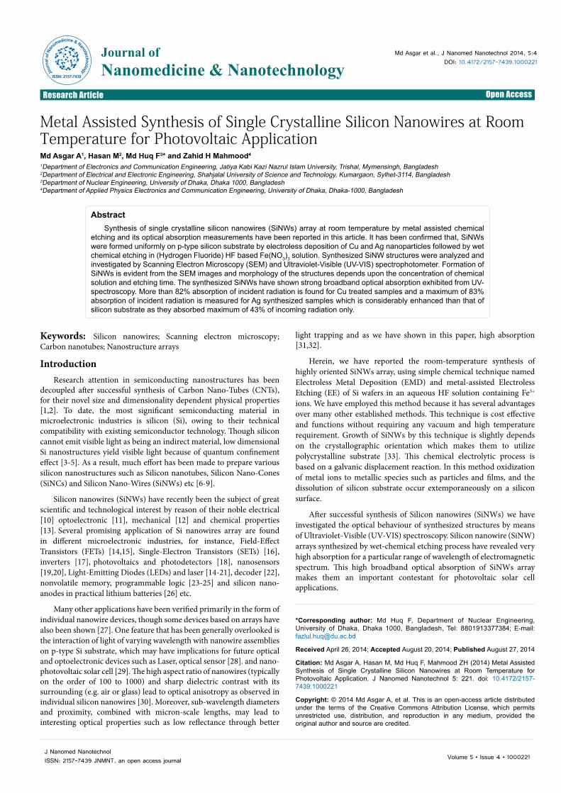
Synthesis Mechanism of Silicon NanowiresFor the initial electroless deposition of silver from HF/AgNO3
solution on silicon, simultaneous electrochemical processes including cathodic (silver-deposition reaction) and anodic reactions (silicon oxidation and dissolution) occur on the silicon surface. First, Ag+ ions in the vicinity of the silicon surface capture electrons from the Valence
Band (VB) of silicon and are deposited in the form of metallic silver nuclei. With the deposition and growth of silver nuclei, SiO2 is formed simultaneously underneath the silver nanoparticles (Illustrated in Figure 1a and b). As the SiO2 underneath the silver nanoparticles is etched away as by HF, then pits are formed immediately at the same location (Illustrated in Figure 1c), so the silver nanoparticles sink into the pits as they are formed. This is consistent with our SEM observations, which confirmed that the oxidation and dissolution of the silicon substrate occur from beneath the metal deposits. In the solution of HF/Fe(NO3)3, the redox level of the Fe3+/ Fe2+ system lies well below the VB of silicon, so active kinetics are expected for the electron-capture process from the VB bonding electrons. However, in contrary to fast reduction of Ag+ ions, reduction of Fe3+ ions and oxidation of silicon proceed very slowly on the silicon surface in the absence of silver nanoparticles. When the silicon surface is covered with silver nanoparticles, reduction of Fe3+ ions and oxidation of silicon are greatly enhanced. It is generally believed that metal nanoparticles adhered on a silicon surface have a higher electronegativity than silicon, so they could attract electrons from silicon to become negatively charged. These metal nanoparticles could then act as local microcathodes and enhance the cathodic reaction as a result of their catalytic activity [34-36]. Therefore, Fe3+ ions have the strong tendency to preferentially obtain electrons from silver nanoparticles and be reduced to Fe2+ ions, while the silicon underneath the silver nanoparticles is oxidized to SiO2 (illustrated in Figure 1d-f). The Ag+/Ag system has more positive redox potential than that of the Fe3+/Fe2+ couple, so silver nanoparticles are stable and can continue to enhance the reduction of Fe3+ ions and the oxidation of silicon in the HF/Fe(NO3)3 solution. As the silver nanoparticles are pinned by the pits and cannot move horizontally on the silicon surface, selective etching occurs and deeper pits or pores finally form (depicted in Figure 1g and 1h).
The following equations explain the chemical reactions that occur in the process:
a b
ed
g h
f
c
Figure 1: A schematic depiction illustrating the electroless deposition of silver on silicon in HF/AgNO3 solution and the silver-nanoparticle-catalyzed chemical etching of silicon in HF/Fe(NO3)3 solution. (a-c) Nucleation and growth of silver nanoparticles on the silicon surface in HF/AgNO3 solution: SiO2 forms simultaneously underneath the silver nanoparticles, and pits form as a result of etching away of SiO2 in HF solution. (d-f) Reduction of Fe3+ ions, etching of silicon, and sinking of silver nanoparticles in HF/Fe(NO3)3 solution: deeper pits are created by the silver nanoparticles. (g) Silver nanoparticle arrays form on the silicon surface. (h) Deep pores form in the bulk silicon in HF/Fe(NO3)3 solution as a result of the continuous etching away of SiO2 underneath the silver nanoparticles [36].

Citation: Md Asgar A, Hasan M, Md Huq F, Mahmood ZH (2014) Metal Assisted Synthesis of Single Crystalline Silicon Nanowires at Room Temperature for Photovoltaic Application. J Nanomed Nanotechnol 5: 221. doi: 10.4172/2157-7439.1000221
Page 3 of 7
Volume 5 • Issue 4 • 1000221J Nanomed NanotechnolISSN: 2157-7439 JNMNT, an open access journal
Ag+ + e- → Ag0(s)
Si(s) + 2H2O → SiO2 + 4H+ + 4e-
SiO2 (s) + 6HF → H2SiF6 +2H2O
Result and DiscussionScanning electron microscopy
Synthesized samples were characterized to scrutinize the structural and optical behaviours. For the structural characterization Scanning Electron Microscope (SEM) image of all prepared samples were taken and the SEM images of metal deposited samples are shown in Figure 2. The solution concentration of HF and AgNO3 were 5 M and 0.02 M respectively for both samples but the deposition time of the first sample was 60 seconds whereas it is 75 seconds for the second one. Highly dispersed silver particles are evident on the silicon substrate in Figure 2. In case of Figure 2b, dispersed silver particles are also appeared like Figure 2a, however in some locations silver clusters look like branched dendrite. As the deposition time is 15 s longer than that of first sample, the density of cluster is higher results silver dendrites. For both samples no regular geometric shape of deposited particles was available.
Figure 2c and d shows the copper nanoparticles that were produced on silicon surfaces by the galvanic displacement reaction on treatment of the silicon wafer in a solution of HF/Cu(NO3)2 for one minute. Deposited particles were approximately 0.2 µm diameter. From the figure it is also obvious that Ag-nanoparticles were deposited more homogeneously than Cu-nanoparticles.
Figure 3 shows the cross-sectional SEM images of silicon nanowires array on p-type Si (111) substrate. The concentration of AgNO3 was 0.02 mol/L in all cases but the nanoparticle deposition time and etching time were different. For Figure 3a and b deposition time was 60 seconds with etching time 45 min and for Figure 3c metal nanoparticle deposition time was the same as Figure 3a and b, 60 seconds, but etching time was increased to 75 min. In case of Figure 3d and e metal (Ag) nanoparticles deposition time was 75 seconds with etching time 60 min. The images plainly indicate that silicon nanowires have formed on the etched
substrate of various sizes. From the given figure it is clearly evident that with higher etching time diameter of synthesized SiNWs decrease because, longitudinal and lateral dissolution occur on Si-substrate as Ag-nanoparticles are pinned by the pits and therefore cannot move horizontally on the silicon surface. SEM observation confirmed that the diameter of nanowire varies from 45 nm to 200 nm and the length from 2 µm to 4 µm approximately. Moreover, with continually increasing of etching time may allow the nanowires to be long and thin enough to be broken apart due to lateral etching illustrated in the Figure 3c. Therefore it can be stated that the morphology of the deposited Ag-particles greatly influence the etching morphology of the Si wafer. The density and size of the as-prepared SiNWs also depend on the distribution patterns of the Ag particles on the Si surface. A high density of Ag particles facilitated the formation of Si nanowires. If the Ag particles are smaller caused by short electroless deposition time, for instance less than 15 seconds, their lift-off or Brownian movement might take place during silicon dissolution, resulting in disordered Si structures [37]. In contrast, stable Ag particles would facilitate the formation of 1D Si nanostructures. The size of the SiNWsis closely related to the space between metal particles and also the immersion time in the HF solution.
The role of Ag particle is also applied for the copper (Cu) nanoparticle with a higher electronegativity than that of silicon. In the case of Cu nanoparticle, high density porous silicon nanostructure arrays were formed and confirmed from the SEM micrograph which is shown in Figure 4. From this SEM morphology, it has been also recognized that silicon nanostructures were formed very uniformly. It has been also evident from the SEM micrograph that, density of SiNWs is smaller in case of 1 hour etching with concentration of Cu(NO3)2 is 0.02 M than that of 2 hours etching through concentration of Cu(NO3)2 is 0.05 M. This may be occurred because of lower density of Cu particle during electroless metal deposition and shorter etching time. Therefore, it can be concluded that with greater deposition time and concentration of the sample solution high density, well oriented SiNWs will be produced. The Cu-nanoparticle may have disappeared from the aqueous HF/Fe(NO3)3 solution, because the standard redox
(a) (b)
(d)(c)
Figure 2: SEM images morphology of electroless Ag-nanoparticle deposited on a p-type Silicon Substrate with axial orientation of (111) from a HF/AgNO3 solution after a treatment (Ag deposition) times of, a) 60 seconds and b) 75 seconds. (c-d) Cu nanoparticles deposition on the same Si substrate with concentration and deposition time of 0.02 M and 60 seconds respectively with different magnification.

Citation: Md Asgar A, Hasan M, Md Huq F, Mahmood ZH (2014) Metal Assisted Synthesis of Single Crystalline Silicon Nanowires at Room Temperature for Photovoltaic Application. J Nanomed Nanotechnol 5: 221. doi: 10.4172/2157-7439.1000221
Page 4 of 7
Volume 5 • Issue 4 • 1000221J Nanomed NanotechnolISSN: 2157-7439 JNMNT, an open access journal
potential of Cu/Cu2+ is lower than that of Fe3+/Fe2+. Cu-nanoparticles would dissolve into the solution as soluble Cu2+ ions, according to the following Equation 1 [37].
2Fe3++Cu(s) → 2Fe2++Cu2+ (1)
UV spectroscopy
The optical properties of SiNWs include reflection, transmission and absorption. Here, optical absorption measurement of SiNWs was carried out over a range of wavelengths 200 nm to 1000 nm, which covers most of the spectrum that is useful for silicon nanowires (SiNWs) based solar cells. Figure 5 shows typical total optical absorption spectra of Cu treated samples: type-A sample (sample-b, sample-c and sample-d) along with absorption of bulk silicon (sample-a). The absorbance of the solid silicon film shows typical behaviour as expected for silicon. Here we have reported that, absorption of bulk Si begins to increase at 400 nm and remains almost steady up to 1000 nm and might be decrease somewhere around 1100 nm because of back reflected loss for long wavelength from the top surface [38]. Solid Si film absorbs maximum of 47% of incident radiation but SiNW arrays absorb maximum 82% of radiation. It has also been observed that the absorbance of the Cu deposited silicon nanowire films increases continually with increasing etching time. The length of SiNWs is directly proportional to the
etching time at a constant concentration of sample solution. Hence, the length of silicon nanowire arrays increase and diameter decrease as the etching time elapses. Therefore, superior quantum confinement of photon occurs and for this reason higher absorption takes place. Previous studies also confirmed that porous silicon, occurs in case of Cu nanoparticle, can reduce back reflection up to 5.8% in the wavelength range of 400-1000 nm, which replace the surface texture to high absorption of photon energy [39-41]. For sample-b etching time and concentration of Cu(NO3)2 are 1 hour and 0.02 M respectively. Whereas, for sample-c and sample-d treating time is 2 hours with concentration of Cu(NO3)2 are 0.02 M and 0.05 M respectively.
From the Figure 5, it has been observed that the absorbance of the Cu deposited silicon nanowires films is much greater than that of the silicon wafer. It has also looked into that with increasing treating time and concentration, higher absorption can be accomplished. However, if the concentration of Cu(NO3)2 is very high then metal nanoparticles would cover the most part of the substrate. SiNWs grow only in the uncovered area of the Si substrate as discussed in Figure 1. So if the metal particle covers almost all surface area of the bulk substrate then the possibility of formation of SiNWs array would be very low and nanowires may not develop if the nanoparticles cover all of the surface area. Otherwise, if the density of the deposited particles is very low then
Figure 3: Cross-sectional SEM image of the synthesized Silicon nanowires array for Ag treated samples. (a-b) Etched for 45 minutes with deposition time of 60 seconds. (c) Etched for 75 min with nanoparticle deposition time 60 seconds. In some location of the substrate, SiNWs are beginning to break apart (shown in the inset) as etching time is increased to 75 minutes. (d-e) Etched for 60 minutes with deposition time of 75 seconds with different magnification.

Citation: Md Asgar A, Hasan M, Md Huq F, Mahmood ZH (2014) Metal Assisted Synthesis of Single Crystalline Silicon Nanowires at Room Temperature for Photovoltaic Application. J Nanomed Nanotechnol 5: 221. doi: 10.4172/2157-7439.1000221
Page 5 of 7
Volume 5 • Issue 4 • 1000221J Nanomed NanotechnolISSN: 2157-7439 JNMNT, an open access journal
the space between them will be large. As a result, silicon microwires (SiMWs) would be produced (similar way as Figure 1) in place of silicon nanowires. Again, if etching time becomes very high then the length of the free standing SiNWs would be fair enough to break apart. Therefore, it can be stated that, an optimum condition of etching time and density of catalytic metal is required for the formation of free standing SiNWs array.
Absorption measurement was also carried out for Ag-synthesized samples: type-B sample (sample-e, sample-f, and sample-g) with different etching time for same wavelength range of 200 nm to 1000
nm which is shown in Figure 6. It has been found that, the absorption of sample-e was very low for wavelength range of 350 nm-1000 nm whereas absorbance increased up to 84% in the range of 200 nm-350 nm. For sample-f and sample-g, absorption of light energy was greater than the silicon wafer in 350 nm to 1000 nm but it was increased tremendously up to 83% in 200 nm to 350 nm.
Based on the above evidence it is clarified that large area single crystalline silicon nanowires (SiNWs) have revealed superior absorption measurement compared to bulk silicon. This high absorption characteristic can be utilized to fabricate absorber in photovoltaic solar
Figure 4: Top view of SEM observation of silicon nanowires (SiNWs) for Cu treated samples. (a, b) 1 hour etching having concentration of Cu(NO3)2 is 0.02 M. (c-f) 2 hours etching using concentration 0.05 M with different magnification. (g-h) Planer SEM micrograph of SiNWs array for Cu treated sample with 1 hour etching time and 0.02 M Cu(NO3)2.

Citation: Md Asgar A, Hasan M, Md Huq F, Mahmood ZH (2014) Metal Assisted Synthesis of Single Crystalline Silicon Nanowires at Room Temperature for Photovoltaic Application. J Nanomed Nanotechnol 5: 221. doi: 10.4172/2157-7439.1000221
Page 6 of 7
Volume 5 • Issue 4 • 1000221J Nanomed NanotechnolISSN: 2157-7439 JNMNT, an open access journal
200 nm to 1000 nm in case of Cu deposited SiNWs. Whereas for Ag, absorbance was maximum 83% which is much greater than that of the bulk silicon as they absorbed maximum 47% of the incidence radiation. This inspection facilitates that the synthesized nanostructure could be a potential contender for efficient photovoltaic (PV) solar cell.
Acknowledgement
Author’s would like to thank Mr. Mahbubul Haq, Director of the Institute of Electronics, Atomic Energy Research Establishment (AERE), Savar, for providing with the Silicon wafer from the project on, “Center of Excellence for the Development of Very Large Scale Integration (VLSI) Technology in Bangladesh” supported by Government of the Peoples Republic of Bangladesh, and to Mrs. Rumana Islam, project fellow in Centre for Advance Research in Science (CARS), University of Dhaka, for her help to work with UV spectrophotometer.
References
1. Iijima S (1991) Helical microtubules of graphitic carbon. Nature 354: 56-58.
2. Poole CP, Owens FJ (2003) Introduction to nanotechnology. John Wiley & Sons, New Jersey.
3. Harrison P (2005) Quantum Wells, Wires and Dots: Theoretical and Computational Physics: John Wiley & Sons, West Sussex.
4. Cao G (2004) Nanostructures & Nanomaterials: Synthesis, Properties & Applications. Imperial College Press, London.
5. Schroder DK (2006) Semiconductor material and device characterization. John Wiley & Sons, Inc., New Jersey.
6. Zhu J, Yu Z, Burkhard GF, Hsu CM, Connor ST, et al. (2009) Optical absorption enhancement in amorphous silicon nanowire and nanocone arrays. Nano Lett 9: 279-282.
7. Wang B, Leu PW (2012) Enhanced absorption in silicon nanocone arrays for photovoltaics. Nanotechnology 23: 194003.
8. Tang YH Pei LZ, Chen YW, Guo C (2005) Self-assembled silicon nanotubes under supercritically hydrothermal conditions. Phys Rev Lett 95: 116102.
9. Fang H Li X, Song S, Xu Y, Zhu J (2008) Fabrication of slantingly-aligned silicon nanowire arrays for solar cell applications. Nanotechnology 19: 255703.
10. Zheng G, Lu W, Jin S, Lieber CM (2004) Synthesis and fabrication of highperformance n-type silicon nanowire transistors. Adv Mater 16: 1890-1893.
11. Qian F, Li Y, Gradecak S, Wang D, Barrelet CJ, et al. (2004) Gallium nitride-based nanowire radial heterostructures for nanophotonics. Nano Lett 4: 1975-1979.
12. Nam CY, Jaroenapibal P, Tham D, Luzzi DE, Evoy S, et al. (2006) Diameter-dependent electromechanical properties of GaN nanowires. Nano Lett 6: 153-158.
13. Zhang Y, Kolmakov A, Chretien S, Meti H, Moskovits M (2004) Control of catalytic reactions at the surface of a metal oxide nanowire by manipulating electrondensity inside it. Nan Lett 4: 403-407.
14. Duan X Huang Y, Cui Y, Wang J, Lieber CM (2001) Indium phosphide nanowires as building blocks for nanoscale electronic and optoelectronic devices. Nature 409: 66-69.
15. Cui Y, Zhong Z, Wang D, Wang WU, Lieber CM (2003) High performance silicon nanowire ?eld effect transistors. Nano Lett 3: 149-152.
16. Zhong Z, Fang Y, Lu W, Lieber CM (2005) Coherent single charge transport in molecular-scale silicon nanowires. Nano Lett 5: 1143-1146.
17. Cui Y Lieber CM (2001) Functional nanoscale electronic devices assembled using silicon nanowire building blocks. Science 291: 851-853.
18. Wang J Gudiksen MS, Duan X, Cui Y, Lieber CM (2001) Highly polarized photoluminescence and photodetection from single indium phosphide nanowires. Science 293: 1455-1457.
19. Hahm J, Lieber CM (2004) Direct ultrasensitive electrical detection of dna and dna sequence variations using nanowire nanosensors. Nano Lett 4: 51-54.
20. Cui Y Wei Q, Park H, Lieber CM (2001) Nanowire nanosensors for highly sensitive and selective detection of biological and chemical species. Science 293: 1289-1292.
cell by preparing a p-n junction on fabricated p-type SiNWs by means of thermal diffusion.
ConclusionIn conclusion, we have demonstrated that Si nanowire films
possess unique macroscopic and optical properties. The nanowires yield significantly increased optical absorption over the full spectrum above the bandgap, as well as reduced transmission for wavelengths of
2.0
1.8
1.6
1.4
1.2
1.0
0.8
0.6
0.4
0.2
0.0200 300 400 500 600 700 800 900 1000
Abs
orpt
ion
Wavelength (nm)
(d)
(c)
(b)
(a)
Figure 5: Illustrating the optical absorption measurement of SiNW arrays along with bulk Si (a) Optical absorption spectrum of p-type Si(111) wafer. (b) Absorption measurement of nanowire arrays using 0.0 2 M Cu(NO3)2 with etching time 1 hour. (c) Absorption image of Cu treated nanowires film using 0.02 M Cu(NO3)2 with etching time 2 hours. (d) Absorbance of nanowires film with etching time 2 hours with 0.05 M Cu(NO3)2.
2.0
1.8
1.6
1.4
1.2
1.0
0.8
0.6
0.4
0.2
0.0200 300 400 500 600 700 800 900 1000
Abs
orpt
ion
Wavelength (nm)
(g)
(f)
(e)
(a)
Figure 6: (a) Optical absorption spectrum of solid Si film. (e) Absorption of Ag deposited nanowires film on Si substrate with etching time 45 min with 0.02 M AgNO3. (f) Absorption data for Ag deposited nanowires film on Si substrate with etching time 60 min having concentration 0.02 M of AgNO3. (g) Absorption measurement for Ag treated Si substrate with etching time 75 min concentration of 0.02 M AgNO3.

Citation: Md Asgar A, Hasan M, Md Huq F, Mahmood ZH (2014) Metal Assisted Synthesis of Single Crystalline Silicon Nanowires at Room Temperature for Photovoltaic Application. J Nanomed Nanotechnol 5: 221. doi: 10.4172/2157-7439.1000221
Page 7 of 7
Volume 5 • Issue 4 • 1000221J Nanomed NanotechnolISSN: 2157-7439 JNMNT, an open access journal
21. Duan X, Huang Y, Agarwal R, Lieber CM (2003) Single-nanowire electricallydriven lasers. Nature 421: 241-245.
22. Zhong Z, Wang D, Cui Y, Bockrath MW, Lieber CM (2003) Nanowire crossbararrays as address decoders for integrated nanosystems. Science 302: 1377-1379.
23. Duan X, Huang Y, Lieber CM (2002) Nonvolatile memory and programmablelogic from molecule-gated nanowires. Nano Lett 2: 487-490.
24. Huang Y, Duan X, Wei Q, Lieber CM (2001) Directed assembly of one-dimensional nanostructures into functional networks. Science 291: 630-633.
25. Huang Y, Duan X, Cui Y, Lauhon LJ, Kim KH, et al. (2001) Logic gates andcomputation from assembled nanowire building blocks. Science 294: 1313-1317.
26. Szczech JR, Jin S (2011) Nanostructured silicon for high capacity lithiumbattery anodes. Energy Environ Sci 4: 56-72.
27. Baxter JB, Aydil ES (2005) Nanowire-based dye-sensitized solar cells. ApplPhys Lett 86: 053114(1-3).
28. Alda J, Rico-García JM, López-Alonso JM, Boreman G (2005) Optical antennas for nano-photonic applications. Nanotechnology 16: 230-234.
29. Sivakov V, Andrä G, Gawlik A, Berger A, Plentz J, et al. (2009) Silicon nanowire-based solar cells on glass: synthesis, optical properties, and cell parameters.Nano Lett 9: 1549-1554.
30. Qi J, Belcher AM, White JM (2003) Spectroscopy of individual silicon nanowires. Appl Phys Lett 82: 2616-2618.
31. Nolan M, O’Callaghan S, Fagas G, Greer JC, Frauenheim T (2007) Siliconnanowire band gap modification. Nano Lett 7: 34-38.
32. Aijiang LU (2007) Theoretical Study of Electronic and Electrical Properties ofSilicon Nanowires, City University of Hong Kong, Thesis (Ph.D.), CityU CallNumber: TK7874.85 .L83 2007.
33. Jung JY, Guo Z, Jee SW, Um HD, Park KT, et al. (2010) A strong antireflective solar cell prepared by tapering silicon nanowires. Opt Express 18 Suppl 3:A286-292.
34. Gorostiza P, Díaz R, Servat J, Sanz F, Morante JR (1997) Atomic ForceMicroscopy Study of the Silicon Doping Influence on the First Stages of Platinum Electroless Deposition. J Electrochem Soc 144: 909-914
35. Teerlinck I, Mertens PW, Schmidt HF, Meuris M, Heyns MM (1996) Impact ofthe electrochemical properties of silicon wafer surfaces on copper outplatingfrom HF solutions. Journal of The Electrochemical Society 143: 3323-3327.
36. Peng K, Wu Y, Fang H, Zhong X, Xu Y, et al. (2005) Uniform, Axial-OrientationAlignment of One-Dimensional Single-Crystal Silicon Nanostructure Arrays.Angewandte Chemie International Edition 44: 2737-2742.
37. Peng K, Hu J, Yan Y, Wu Y, Fang H, et al. (2006) Fabrication of Single-Crystalline Silicon Nanowires by Scratching a Silicon Surface with CatalyticMetal Particles. Advanced Function Materials 16: 387-394.
38. Tsakalakos L, Balch J, Fronheiser J, Shih MY, LeBoeuf SF, et al. (2007)Strong broadband optical absorption in silicon nanowire films. Journal of Nanophotonics 1: 013552(1-10).
39. Ron I, Friedman N, Cahen D, Sheves M (2008) Selective electroless deposition of metal clusters on solid-supported bacteriorhodopsin: applications toorientation labeling and electrical contacts. Small 4: 2271-2278.
40. Stelzner T, Pietsch M, Andrä G, Falk F, Ose E, et al. (2008) Silicon nanowire-based solar cells. Nanotechnology 19: 295203.
41. X Li (2012) Metal assisted chemical etching for high aspect ratio nanostructures: A review of characteristics and applications in photovoltaics. Current Opinion in Solid State and Mat Sci 16: 71-81.