jpeg image decoder ece 511 project final reportelliott/ece511/projects/2004f/jpeg...ece 511 2d-idct...
TRANSCRIPT

ECE 511 2D-IDCT 1/66
JPEG Image Decoder ECE 511 Project
Final Report
December 5, 2004
Maziyar Khorasani ([email protected]) Ramkrishna Swamy ([email protected])
Yongjie Liu ([email protected]) Rejean Lau ([email protected])

ECE 511 2D-IDCT 2/66
Declaration of Original Content The design elements of this project and report are entirely the original work of the authors and have not been submitted for credit in any other course except as follows: - The architectural description of the modified Loeffler algorithm was taken from [1]. - The color space converter was modified from [3]. - The C source code to decompress the JPEG file was taken and modified from [4]. _________________ _________________ Maziyar Khorasani Yongjie Liu _________________ _________________ Ramkrishna Swamy Rejean Lau

ECE 511 2D-IDCT 3/66
Abstract JPEG is a popular compression algorithm that can compress image files very efficiently. It a lossy, yet very robust, compression scheme that takes advantage of pitfalls of human perception. A 2D Inverse Discrete Cosine Transform (2D-IDCT) block was designed and was used to output a decompressed JPEG image to screen using 24-bit color depth. The project mixes software and hardware modules to fully decompress the JPEG image file. This document describes the design and simulation of Loeffler’s algorithm for the 2D-IDCT and how the peripheral components on the Virtex II Multimedia board were interfaced to produce a functional JPEG decoder unit.

ECE 511 2D-IDCT 4/66
TABLE OF CONTENTS ABSTRACT................................................................................................................................... 3
TARGET FPGA............................................................................................................................ 6
ACHIEVEMENTS........................................................................................................................ 7
INTRODUCTION......................................................................................................................... 8
DESCRIPTION OF DESIGN AND OPERATION................................................................... 9 SYSTEM OVERVIEW ..................................................................................................................... 9 IMAGE PREPROCESSING ............................................................................................................. 11
DCT Coefficient Size............................................................................................................. 12 Software IDCT: Processing Time ......................................................................................... 12
LOADING IMAGE INTO BLOCK RAM.......................................................................................... 12 2D IDCT OPERATION................................................................................................................ 13
Results from Experiments & Characterization – Math Model ............................................. 13 Implementation Details......................................................................................................... 14
TRANSPOSE MEMORY ................................................................................................................ 19 READ/WRITES TO YCBCR MEMORY.......................................................................................... 20 YCBCR TO RGB CONVERSION .................................................................................................. 20 RGB OUTPUT ............................................................................................................................ 20
FILE HIERARCHY ................................................................................................................... 21
FINAL DEVELOPMENT STATUS ......................................................................................... 22
DESIGN CONSIDERATIONS.................................................................................................. 23
FPGA LOGIC AND MEMORY USAGE................................................................................. 25
SYNTHESIS REPORTS ............................................................................................................ 26 RESOURCE REQUIREMENTS........................................................................................................ 26
VGA Top Level ................................................................................................................... 26 2D-IDCT............................................................................................................................... 28 IDCT Top Level................................................................................................................... 28 IDCT Control Unit ............................................................................................................... 29 IDCT Data Path .................................................................................................................. 29
STATIC TIMING ANALYSIS ......................................................................................................... 30
DESIGN VERIFICATION ........................................................................................................ 32 INDEX AND DESCRIPTION OF TEST CASES.................................................................................. 32 VHDL COMPONENTS ................................................................................................................ 32 TESTBENCHES & SIMULATIONS ................................................................................................. 34
APPLICATION SPECIFIC INTEGRATED CIRCUIT (ASIC) RESULTS ........................ 36
FPGA PINOUT INFORMATION ............................................................................................ 39
REFERENCES............................................................................................................................ 40
APPENDIX A: CODE INDEX .................................................................................................. 41

ECE 511 2D-IDCT 5/66
GLOBALS_PKG.VHD ................................................................................................................... 42 IDCT_1D_TOP.VHD..................................................................................................................... 43 ROTATOR.VHD ........................................................................................................................... 44 BUTTERFLY.VHD........................................................................................................................ 45 MULTIPLY.VHD.......................................................................................................................... 46 ADD_SUB.VHD ........................................................................................................................... 47 TRANSPOSE_MEMORY.VHD ........................................................................................................ 48 TRANSPOSE_BUFFERS.VHD......................................................................................................... 49 IDCT_DATAPATH.VHD ................................................................................................................ 51 IDCT_CONTROL_UNIT.VHD......................................................................................................... 52 YCBCR_RGB_CONV.VHD.......................................................................................................... 53 GET_RAM_DATA24_256.RGB................................................................................................... 54 SVGATIMINGGENERATION.V ............................................................................................ 55
APPENDIX B: TESTBENCH AND SIMULATIONS ............................................................ 56 TOP_LEVEL_TB.VHD .................................................................................................................. 57 IDCT_1D_TOP_TB.VHD ............................................................................................................... 58 ROTATOR_TB.VHD ..................................................................................................................... 59 BUTTERFLY_TB.VHD.................................................................................................................. 60 MULTIPLY_TB.VHD.................................................................................................................... 61 ADD_SUB_TB.VHD ..................................................................................................................... 62 TRANSPOSE_MEMORY_TB.VHD.................................................................................................. 63 TRANSPOSE_BUFFERS_TB.VHD .................................................................................................. 64 YCBCR_RGB_CONVERTER_TB.VHD ......................................................................................... 65 VGA SYSTEM OUTPUT .............................................................................................................. 66

ECE 511 2D-IDCT 6/66
Target FPGA We were given permission to implement our design on the Virtex II Multimedia board. This specific board uses the XCV2000 FPGA, allowing for designs utilizing up to two million gates. Of more interest, this board comes equipped with:
- an on-board Ethernet port, - a 24-bit color depth VGA port, - an array of three DACs, - compact flash card access (16MB) and - five fully independent banks of 512K x 36 of on-board ZBT SRAM.
This board is an ideal solution for this project since our design is large and physically more demanding.

ECE 511 2D-IDCT 7/66
Achievements During the course of this project, we were able to accomplish several milestones. However, our initial proposal statements were not met due to problems associated with the board and related software. The following lists our achievements: - Created a functional 2D IDCT block by implementing two 1D IDCT Blocks with 4 transpose
buffers. - Implemented an 8 bit YCbCr to RGB converter. - Successfully interfaced the Virtex II Multimedia Board to a VGA monitor, capable of
displaying required data and images by implementing a VHDL VGA controller on top of Verilog design.
- Successfully implemented the interface between the MicroBlaze to both the CompactFlash and ZBT RAM on the Virtex II Multimedia board through the OPB Bus.
- Created a top-level controller to access the ZBT RAM directly through VHDL/Verilog rather than through the MicroBlaze OPB Bus.
- Created a top-level entity to interface to the provided Virtex II Multimedia IP Cores (like the Block RAM, multipliers and adders).

ECE 511 2D-IDCT 8/66
Introduction The human eye is a wondrous tool that allows bestows the gift of sight to humanity; however, as with all things, it has its weaknesses, and this weakness is what JPEG image compression exploits. JPEG Image compression uses DCT (Discrete Cosine Transform) encoding to break an image into component frequencies. It breaks an image into 8x8 blocks (a matrix of 64 coefficients) and transforms the spatial data into low and high-frequency coefficients in the frequency domain. The goal then is the discard the high-frequency data, the values in the frequency domain that the human eye cannot clearly distinguish, while at the same time maintaining the more (humanely) visible low-frequency data. The discarding of the higher-frequency data through Quantization and Entropy Encoding allows for a substantial compression of an image. Quantization basically is where a substantial amount of the transformed data can be removed, then further implementations of Entropy Encoding (Run Length Encoding) further decreases the image size. The compressed image then follows a similar but reverse series of steps where by using an IDCT (Inverse Discrete Cosine Transform) and several decoding schemes, the image can be decompressed, exhibiting some loss in image quality. This project implements Loeffler’s algorithm for the IDCT using the Virtex II Multimedia board. It completes the final image decompression step and displays the resulting image onto a VGA monitor.

ECE 511 2D-IDCT 9/66
Description of Design and Operation System Overview The JPEG Decoder Core takes a parsed JPEG image file containing the outputs of the DCT. These (YCbCr) pixel coefficients are then loaded directly into the block ram by passing it along the bit stream during the programming of the FPGA. The system will immediately begin to process the image and will display the decoded image almost instantly on the VGA output. The reset pin can be used to restart the image decoding and display process. The system is composed of the following units: - 2D IDCT core consisting of the following units
- Two 1D IDCT cores and 4 transpose buffers - 4 banks of 64x128 Block RAM and 1 bank of 24x256 Block RAM - VGA Control unit capable of outputting variable size images to the screen in true 24 bit color The JPEG Decoder Core Top Level diagram is shown below in Figure 1.
There are two inputs into this unit, the pixel_clk and the reset. The pixel_clk not only acts as the main system clock but is also the clock used by the VGA Controller to display the image at 50 MHz. The reset signal is simply used to reset the unit such that it can restart the JPEG decoding and image display operation. The output signals are all used simply to display the decoded image through a VGA connection (eg. computer monitor, projector). The system is broken up into several smaller components as demonstrated in Figure 2. The internal components and the preparation of the image for decoding will not be described.
JPEG DECODER CORE
pixel_clk
reset
pixel_clk_out
blank
comp_synch
h_synch_delay
v_synch_delay
R
G
B
8
8
8
Fig 1 JPEG Decoder Core Top Level

ECE 511 2D-IDCT 10/66
Control Unit
br_read_en
br_read_addr
Idct_reset
idct_datain_valid
Source Block RAM
(64x128)
addr
din
we
en
dout 64
2D IDCT
din
br_write_addr_CU
br_write_Y_en_CU
br_write_Cb_en_CU
br_write_Cr_en_CU
VGA Top Level Controller
br_write_addr_VGA
br_write_Y_en_VGA
br_write_Cb_en_VGA
br_write_Cr_en_VGA
Y Destination Block RAM
(64x128)
addr
din
we
en
dout
64
br_write_we_CU
br_write_we_VGA
Cb Destination Block RAM
(64x128)
addr
din
we
en
dout
64
Cr Destination Block RAM
(64x128)
addr
din
we
en
dout
64
dout
64
din
64
YCbCr_Data_Ready
RBG Block RAM
(24x256)
addr
din
we
en
dout
24
24 Data Path
pixel_clk
reset
pixel_clk_out
blank
R
G
B
8
8
8
comp_synch
h_synch_delay
v_synch_delay
Fig 2 High Level Internal System Block Diagram

ECE 511 2D-IDCT 11/66
Image Preprocessing The JPEG decoding C program [4] is capable of decompressing a JPEG file into BMP file. Basically, it consists of Huffman decoding, dequantization, IDCT transform and transform YCbCr to RGB. We modify the decoding C program and make it the pre-processing module for our project. Generally, the pre-processing module is complied and running on a PC. Table 1 describes the input/output of the pre-processing module.
Type Purpose Description JPEG source file Input (.jpg) - The original compressed JPEG file, DCT coefficient data file
Output (.coe) Input for the IDCT core
This file contains all the coefficients generated from the JPEG source file by the decoding program.
YCbCr data file Output (.coe) For the functional testing of IDCT core
This files contains the Y Cb Cr values generated by the IDCT function in the C program
RGB data file Output (.coe) For functional testing of VGA output module
This file contains the RGB values extracted from the final BMP file, which is the original output the decoding program.
Table 1: Preprocessing module The hierarchy of the pre-processing program is shown in the figure below:
Huffman decodingJPEG source
DCT coefficient file
Dequantization
IDCTYCbCr to RGB YCbCr data file
RGB data file

ECE 511 2D-IDCT 12/66
DCT Coefficient Size The DCT coefficient size has a great impact on the processing speed of the IDCT core. The longer the bit length of the DCT coefficient, the more processing time of IDCT core. In order to gain faster speed while preserving acceptable decoded image quality, we placed constraints in the C program to reduce the coefficient size or bit length. The original size is 16 bits signed. With several experimental testing, we are able to know that 8 bit signed value can achieve the best trade off between speed and quality. Software IDCT: Processing Time In the pre-processing program, we also measured the processing speed (i.e., time elapsed) for IDCT function. The timing measurements are used to compare with our IDCT core’s performance. .COE format description IDCT coefficient file: Each line contains 8 hex numbers. Every hex number represents a DCT coefficient value. All DCT coefficients of R are placed first, then B’s, finally G’s. For a 16x16 image, there are total 96 lines. YCbCr data file: Each line contains ‘x’ hex numbers, where x is the image width. All DCT coefficients of R are placed first, then B’s, finally G’s. RGB data file: Each line contains 3 decimal values, which are R, G, and B values for one pixel. There are totally x lines, where x is the number of total pixels in the image. Loading Image into Block RAM The processed image (containing the DCT coefficients) is loaded directly into the block ram via a COE file. During creation of the block ram from the IP core, there is an option to pre-load the ram from an external COE file. By selecting this option, we are able to easily pre-load the RAM. This had the advantage that it is simple and quick, but the disadvantage that data can only be statically loaded and not dynamically during run time.

ECE 511 2D-IDCT 13/66
2D IDCT Operation Results from Experiments & Characterization – Math Model We modeled our 2D-IDCT using Matlab to prove the functionality and accuracy of the algorithm. In the model, Loeffler’s algorithm was tested and compared against the built-in IDCT function from Matlab. More specifically, we provided an input matrix to both cases and evaluated the result. Using the following results, our implementation was proved to be sufficiently accurate.
in_matrix = 127 39 21 7 0 0 0 0 42 23 1 6 0 0 0 0 19 89 3 0 0 0 0 0 4 77 100 0 0 0 0 0 6 66 2 0 0 0 0 0 0 0 0 0 0 0 0 0 0 0 0 0 0 0 0 0 0 0 0 0 0 0 0 0 from_matlab = 113 87 49 14 -7 -13 -13 -10 28 26 23 23 24 23 19 15 -29 -15 7 30 44 44 34 24 -5 1 11 21 27 27 20 15 37 25 9 -2 -4 3 13 20 38 23 1 -15 -15 -1 19 33 21 16 9 3 2 6 11 15 14 20 28 30 23 8 -9 -20 our_model_descaled = 111 85 48 14 -6 -13 -12 -10 27 25 23 23 24 23 18 15 -29 -15 8 30 44 44 33 24 -5 1 11 21 27 27 21 15 37 25 9 -2 -4 3 13 20 39 23 1 -14 -15 -1 19 33 21 16 9 4 2 6 12 16 14 20 28 31 24 9 -8 -20

ECE 511 2D-IDCT 14/66
The following is our scaling matrix: ans = 8 8 8 8 7 8 7 8 8 8 8 8 8 8 8 8 8 8 9 8 8 8 8 8 8 7 8 8 8 8 8 8 8 8 8 10 9 7 8 8 8 8 7 8 8 8 8 8 8 8 8 9 9 8 8 8 8 8 8 8 8 9 7 8 The following is our error matrix: error = -2 -2 -1 0 1 0 1 0 -1 -1 0 0 0 0 -1 0 0 0 1 0 0 0 -1 0 0 0 0 0 0 0 1 0 0 0 0 0 0 0 0 0 1 0 0 1 0 0 0 0 0 0 0 1 0 0 1 1 0 0 0 1 1 1 1 0
The scaling matrix represents a set of values that the “our_model” matrix was scaled by, ie. scale_matrix * from_matlab = our_model. These scaled values should not cause any grief, as it would enhance the intensity in the pixel block. It must be noted that the upper part (low frequency) of the scale matrix is constant, whereas the lower (high frequency) components differ by a small amount. This would not affect the result since the human eye is more tuned to lower frequency data. It should also be noted that our error matrix is very small. That is, we are within a 1% range of the actual value. Implementation Details To correctly convert the DCT matrix from spatial frequency domain to the normal space domain, we must apply the N-point 1D-IDCT transformation for each row in the DCT.

ECE 511 2D-IDCT 15/66
This can be expressed as [1] In Equation 1, Xu represent the transformed inputs and xi represents the outputs. To fully reverse-transform the DCT matrix, we must complete 16 iterations of the 1D-IDCT (Equation 1) – eight iterations for each row in the DCT matrix and another eight iterations for each column of the resulting matrix. Equation 1 is to be implemented in the following manner, as proposed by the modified Loeffler algorithm:
We will have eight simultaneous inputs to the system and have eight simultaneous outputs result, on the right hand side of the diagram. This diagram notation makes use of what is known as the Butterfly – each crossover point has a formula associated with it.
( )
8otherwise 1
0for 21
where
212cos2
2
1
0
=
=
=
+= ∑
−
=
N
uK
NuiXK
Nx
u
N
u
uuiπ
Equation 1:Loeffler's 1D-IDCT
Figure 3 Loeffler’s 1D-IDCT datapath taken from [1]
Figure 4 Butterfly block taken from [1]

ECE 511 2D-IDCT 16/66
Each square block in the diagram, known as the ‘Rotator’, has the following format [1]:
The inputs and outputs to this block correspond to the following:
This operation could be implemented a couple of different ways – three multiplications and three additions or four multiplications and 2 additions. We choose the latter (as suggested by [1]) since it reduces the critical path and improves numerical accuracy.
Figure 5 Rotator block taken from [1]
10101
10100
16cos
16sin
16sin
16cos
ICISnkInkIO
ISICnkInkIO
nn
nn
′+′=+=
′−′=−=
ππ
ππ
Equation 2 Rotator block calculations
Figure 6 Rotator implementation taken from [1]
ECE 511 2D-IDCT 17/66
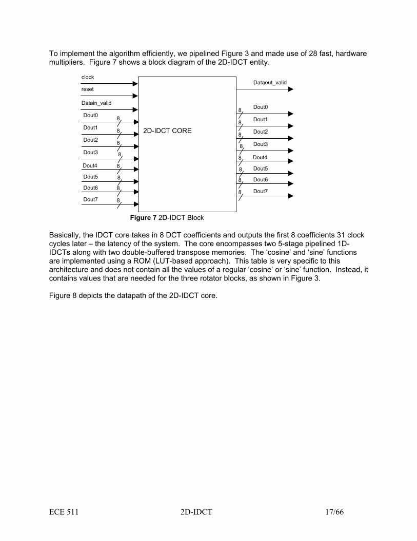
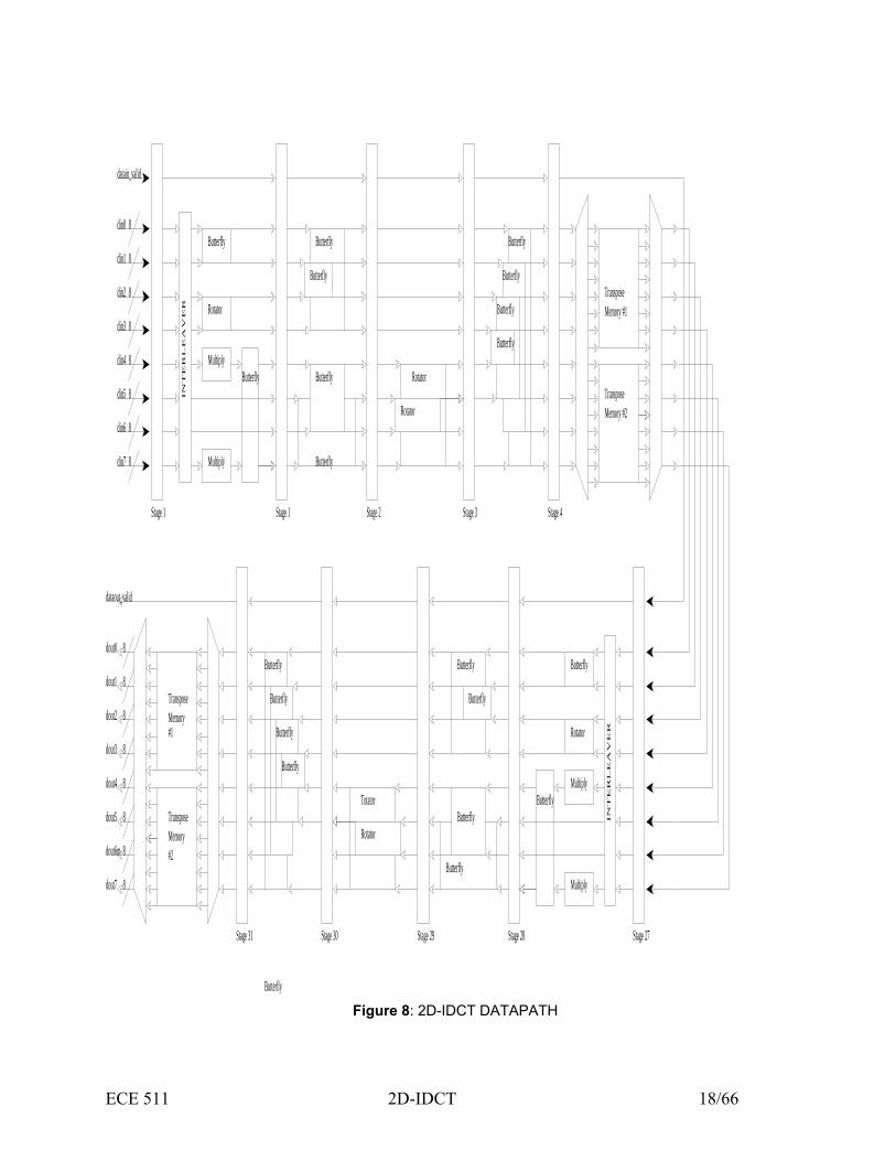
To implement the algorithm efficiently, we pipelined Figure 3 and made use of 28 fast, hardware multipliers. Figure 7 shows a block diagram of the 2D-IDCT entity. Basically, the IDCT core takes in 8 DCT coefficients and outputs the first 8 coefficients 31 clock cycles later – the latency of the system. The core encompasses two 5-stage pipelined 1D-IDCTs along with two double-buffered transpose memories. The ‘cosine’ and ‘sine’ functions are implemented using a ROM (LUT-based approach). This table is very specific to this architecture and does not contain all the values of a regular ‘cosine’ or ‘sine’ function. Instead, it contains values that are needed for the three rotator blocks, as shown in Figure 3. Figure 8 depicts the datapath of the 2D-IDCT core.
2D-IDCT CORE
clock
reset Dataout_valid
Dout0
Dout1
Dout2
Dout3
Dout5
Dout6
Dout7
8
Figure 7 2D-IDCT Block
8
8
8
8
8
8
8
Dout4
Dout0
Dout1
Dout2
Dout3
Dout5
Dout6
Dout7
8
8
8
8
8
8
8
8
Dout4
Datain_valid
ECE 511 2D-IDCT 18/66
Multiply
Multiply
8
8
8
8
8
8
8
8
Stage 1 Stage 1 Stage 3 Stage 4
TransposeMemory #1
TransposeMemory #2Rotator
Rotator
Rotator
Butterfly
Butterfly Butterfly
Butterfly
Butterfly
Butterfly Butterfly
Butterfly
Multiply
Multiply
Rotator
Butterfly
Butterfly
Rotator
Totator
IN
TE
RL
EA
VE
R
IN
TE
RL
EA
VE
R
datain_valid
din0
din1
din2
din3
din4
din5
din6
din7
Stage 2
Stage 31 Stage 30 Stage 29 Stage 28 Stage 27
dout0
dout1
dout7
dout6m
dout5
dout4
dout3
dout2TransposeMemory#1
TransposeMemory#2
dataout_valid
8
8
8
8
8
8
8
8
Butterfly
Butterfly
Butterfly
Butterfly
Butterfly
Butterfly
Butterfly
Butterfly
Butterfly
Butterfly
Butterfly
Figure 8: 2D-IDCT DATAPATH

ECE 511 2D-IDCT 19/66
Transpose Memory The transposition memory consists of an 8x8 register array in which each register is 8 or 18 bits long depending on the stage of calculation. The inputs to the transpose can either be 8 8-bit or 18-bit values. Eight clock cycles after receiving the last input, there will either be 8 8-bit and 18-bit outputs. The above structure acts as a memory transpose unit by taking in 8 inputs at a time, then shifting them down on every cycle. Once all 8 rows have been filled, the select line goes low, and on each clock, the transposed values can be output 1 at a time (for a total of 8 clock cycles to get all 8 values out). The IDCT unit controls the data movement through rowen and colen signals that are then mapped to a select line that controls the multiplexers.
Fig 9 Transpose Memory

ECE 511 2D-IDCT 20/66
Read/Writes to YCbCr Memory Out of the 2D IDCT, the data arrives in order Y then Cb then Cr. This data is then mapped to three different block ram banks, a Y, Cb, and a Cr block memory bank. The control unit logic in the Top Level entity is responsible for determining what addresses the data should be written too and which memory bank and in which order. Also, referencing Figure 2, we can see that mux’s are used to signal when either the control unit is writing/reading from the Block RAMS or the VGA controller is reading/writing from the RAMS. YCbCr to RGB Conversion For correct VGA monitor output, the color space needs to be converted from Y’CrCb color space to the RGB color space. A 10 bit behavioral implementation was modified using the following conversion equations supporting 8 bit conversion: R’=1.164(Y’-16) + 1.596(Cr-128) G’=1.164(Y’-16) – (0.813)(Cr-128) –0.392(Cb-128) B’=1.164(Y’-16) + 2.017(Cb-128) A fast pipelined converted with a max frequency of 153.563 MHz (latency of 3) was synthesized. Choice of design was made considering no memory resource requirements (compared to lookup table based) and fast performance. Correctness was verified, by comparing with the 10 bit implementation, some sample conversion tests testing overflows, negative values, and correct conversion. RGB Output An elegant design resulted in the challenge of creating a VGA controller in VHDL. A low level verilog was available on the Xilinx web site, and had a bug preventing correct operation (reverse blanking signal), which was subsequently corrected and fixed. Upon this, the challenge was to compile a mixed HDL design, so that low level timing information (Vsync, Hsync, Blank, Pixel Clock, and Comp) could be passed to the higher top level VHDL entity for pin routing. However, it was also necessary, to add some additional control counters, tracking pixel locations, so that the 16 x 16 pixel image could be displayed anywhere on the screen. This was implemented in a VHDL wrapper level, on top of the Verilog component, which served as the application user interface. Using such a layered approach, provided an elegant way of interfacing the controller with the application, and keeping low level timing information (synch settings) at a lower level of abstraction.

ECE 511 2D-IDCT 21/66
File Hierarchy
Globals_pkg.vhd idct_toplevel.vhd
IDCT_CONTROL_Unit.vhd IDCT_DATAPATH.vhd
VGA_Top_level.vhd
get_ram_data24_256_RGB.vhd
SVGATIMINGGENERATION.v
YcbCr_RGB_converter.vhd
block_ram_destination.vhd Block_ram_source.vhd
idct_2d.vhd
transpose_buffers.vhd
transpose_memory.vhd
idct_1d.vhd
butterfly.vhd
add_sub.vhd
rotator.vhd
multiply.vhd
ECE 511 2D-IDCT 22/66
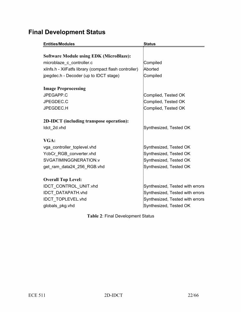
Final Development Status
Entities/Modules Status Software Module using EDK (MicroBlaze): microblaze_c_controller.c Compiled xilnfs.h - XilFatfs library (compact flash controller) Aborted jpegdec.h - Decoder (up to IDCT stage) Compiled Image Preprocessing JPEGAPP.C Complied, Tested OK JPEGDEC.C Complied, Tested OK JPEGDEC.H Complied, Tested OK 2D-IDCT (including transpose operation): Idct_2d.vhd Synthesized, Tested OK VGA: vga_controller_toplevel.vhd Synthesized, Tested OK YcbCr_RGB_converter.vhd Synthesized, Tested OK SVGATIMINGGNERATION.v Synthesized, Tested OK get_ram_data24_256_RGB.vhd Synthesized, Tested OK Overall Top Level: IDCT_CONTROL_UNIT.vhd Synthesized, Tested with errorsIDCT_DATAPATH.vhd Synthesized, Tested with errorsIDCT_TOPLEVEL.vhd Synthesized, Tested with errorsglobals_pkg.vhd Synthesized, Tested OK
Table 2: Final Development Status

ECE 511 2D-IDCT 23/66
Design Considerations Pipelining Architecture:
The 2D IDCT Architecture employed to make this process efficient is described below. Before the process is described, it is worth noting several key points: The 1D IDCT is a 5 stage pipeline The Transpose Memory (TM) takes 8 rows per 8 clock edges (i.e. 1 row/clock) and outputs 1 column/clock. Now, initially, 2 banks of memory are used to store the image. The rows of each 8x8 matrix are split between the two banks, 4 row elements in one bank and the other 4 elements in the other bank. Thus by using 2 separate memory banks, each connected via a separate bus, we can then read in one full row per clock cycle. The 1D IDCT is pipelined into 5 stages, and thus to make use of this pipeline, an 8 value row had to be input into it on every clock. This was achieved by using the 2 banks of initial memory. The 5-stage pipeline gives us an IDCT value every cycle then once the pipeline has been filled. The output of the first 1D IDCT is then fed to the transpose memory such that the rows can be transposed to columns. The transpose memory takes in a row on each clock, then once 8 rows have been entered into the TM, on every clock after that, the transposed 8 values are then output to the second ID IDCT. Two transpose memory buffers are used in order to allow the IDCT 5 stage pipelines to be used to their maximum capacity, as it takes 8 cycles for data to come in and 8 cycles for data to come out, if the second TM was not present, the 1D IDCT would have had to wait for 8 cycles. This was, switching back and forth between the two TM’s, we can efficiently use the pipeline.
Memory Y1 Y2 Y3 Y4
Cb1 Cb2 Cb3 Cb4 Cr1 Cr2 Cr3 Cr4
Y5 Y6 Y7 Y8 Cb5 Cb6 Cb7 Cb8 Cr5 Cr6 Cr7 Cr8
Memory Y1 Y2 Y3 Y4
Y5 Y6 Y7 Y8
Cb1 Cb2 Cb3 Cb4 Cb5 Cb6 Cb7 Cb8
Cr1 Cr2 Cr3 Cr4 Cr5 Cr6 Cr7 Cr8
1D IDCT (5 stage)
TM
TM
1D IDCT (5 stage)
TM
TM
ECE 511 2D-IDCT 24/66
Again, the outputs second 1D IDCT go to the next 2 stage TM for the same reason as before, then finally after the TM, the transformed values are ready to be written to memory. Again, for efficiency in the VGA output stage, the Y, Cb and Cr values are written to different memory banks, allowing future access to them in parallel. This however results in only 3 writes of 32 bits each. Thus, we can only write 4 row values at per write. This would result in an overrun of our data since more data is being produced then is being written. This problem is resolved by clocking the memory at a faster speed then the IDCT, more precisely 2 times as fast. This allows us to do 2 writes to the memory per every output of the TM. Efficiency Calculations: Now assuming for an 800x600 pictures: 480000 pixels. At 3 reads/8 row pixels (since each pixel has a corresponding Y, Cb or Cr value) 480000*3/8 = 180000 Thus 180000 memory reads for an 800x600 picture. Now it takes 5 clock cycles per 1D IDCT, and 16 clock cycles per TM component. Thus a total of (2*5 + 2*16 =) 42 clock cycles for data to move through from when its been read from memory to when it is ready to be written. Thus it takes 180042 clock cycles for the entire 800x600 image to be processed. This process, clocked at 102 MHz will thus take 180042/(102 x10^6) = 0.001765 seconds for completion of an 800x600 picture.

ECE 511 2D-IDCT 25/66
FPGA Logic and Memory Usage The memory resources consumed by the synthesized (VHDL) system is shown in Table 3. Memory Type Size Data Used by Single Port Block Ram
64 bits wide x 96 rows deep
DCT Coefficients produced by C program
Idct_2d.vhd
Single Port Block Ram
64 bits wide x 32 rows deep
Y Idct_1d.vhd vga_controller_toplevel.vhd
Single Port Block Ram
64 bits wide x 32 rows deep
Cr Idct_1d.vhd vga_controller_toplevel.vhd
Single Port Block Ram
64 bits wide x 32 rows deep
Cb Idct_1d.vhd vga_controller_toplevel.vhd
Single Port Block Ram
24 bits wide x 256 rows deep
RGB vga_controller_toplevel.vhd
TOTAL 2.25 Kilobytes Table 3: Memory resources consumed for synthesized system A total memory usage was 2.25 kilobytes consumed for the processing of a 16x16 pixel image.

ECE 511 2D-IDCT 26/66
Synthesis Reports Compiled for Target Device : xc2v2000-5-ff896 Resource Requirements Entities/Modules Synthesis Report
YcbCr-to-RGB Converter:
YcbCr_RGB_converter.vhd
8 20 bit register 3 8 bit register 2 20 bit subractor 2 20 bit adder 3 9 bit subtractor 5 9x11 bit multipliers 184 FF
Number of Slices : 126 Number of Slice Flip Flops : 184 Number of 4 input LUTs: 164 Number of MULT18X18 : 5 Bonded IOB: 49 GCLKs : 1
VGA Timing Generator SVGATIMINGGENERATION.v
3 11-bit up counter 1 10 bit up counter 1 20 bit up counter 1 20 bit up counter 20 1 bit register 1 1 bit xor2
Number of Slices : 59 Number of Slice Flip Flops : 63 Number of 4 input LUTs: 112 Number of bonded IOBs: 28 Number of GCLKs: 1
VGA Top Level vga_top_level.vhd
48 1 bit register 1 2 bit register 9 20 bit register 4 32 bit register

ECE 511 2D-IDCT 27/66
3 5 bit register 9 8 bit register 1 9 bit register 5 9x11 bit multiplier 1 20 bit comparator 1 20 bit comparator not equal 2 32 bit comparator greatequal 6 32 bit comparator comparator greater 2 32 bit comparator less 5 32 bit comparator lessequal
Number of Slices : 671 Number of Slice Flip Flops : 571 Number of 4 input LUTs: 1208 Number of bonded IOBs: 65 Number of BRAMS: 4 Number of MULT18x18s: 5 Number of GCLKs: 1
1D-IDCT:
Idct_1d_top.vhd
6 1-bit registers 8 12-bit registers 40 18-bit register 14 2-to-1 multiplexer
Number of Slices: 726 Number of Slice Flip Flops: 750 Number of 4 input LUTs: 668 Number of bonded IOBs: 195 Number of MULT18X18s: 14 Number of GCLKs: 1
Butterfly.vhd
Number of Slices: 22 Number of 4 input LUTs: 40 Number of bonded IOBs: 72
Rotator.vhd
Number of Slices: 26 Number of 4 input LUTs: 48 Number of bonded IOBs: 108 Number of MULT18X18s: 4
Multiply.vhd 1 2-to-1 multiplexer
Number of Slices: 11 Number of 4 input LUTs: 20 Number of bonded IOBs: 55 Number of MULT18X18s: 1
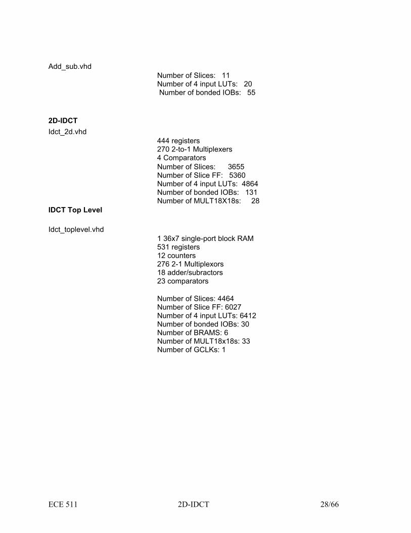
ECE 511 2D-IDCT 28/66
Add_sub.vhd
Number of Slices: 11 Number of 4 input LUTs: 20 Number of bonded IOBs: 55
2D-IDCT Idct_2d.vhd
444 registers 270 2-to-1 Multiplexers 4 Comparators
Number of Slices: 3655 Number of Slice FF: 5360 Number of 4 input LUTs: 4864 Number of bonded IOBs: 131 Number of MULT18X18s: 28
IDCT Top Level Idct_toplevel.vhd
1 36x7 single-port block RAM 531 registers 12 counters 276 2-1 Multiplexors 18 adder/subractors 23 comparators
Number of Slices: 4464 Number of Slice FF: 6027 Number of 4 input LUTs: 6412 Number of bonded IOBs: 30 Number of BRAMS: 6 Number of MULT18x18s: 33 Number of GCLKs: 1

ECE 511 2D-IDCT 29/66
IDCT Control Unit
1 FSM 2 32x32 bit multipliers 9 adder/subtractors 2 registers 11 latches 2 comparators 2 32 bit 2-1 multiplexors
Number of Slices: 300 Number of Slice FF: 192 Number of 4 input LUTs: 555 Number of bonded IOBs: 22 Number of MULT18x18s: 2 Number of GCLKs: 1
IDCT Data Path
444 registers 274 multiplexers 4 comparators
Number of Slices: 3655 Number of Slice FF: 5360 Number of 4 input LUTs: 4875 Number of bonded IOBs: 52 Number of MULT18x18s: 28 Number of GCLKs: 1
Table 4: Synthesis Report for Components
ECE 511 2D-IDCT 30/66
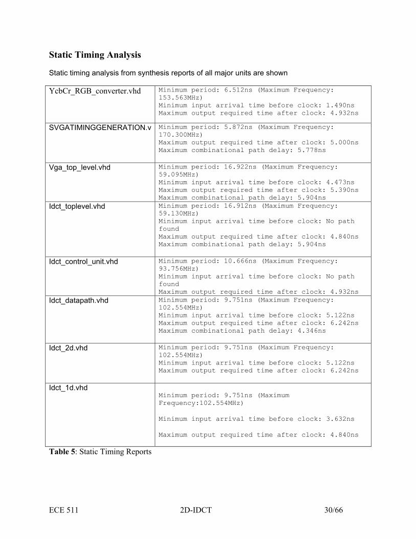
Static Timing Analysis Static timing analysis from synthesis reports of all major units are shown YcbCr_RGB_converter.vhd
Minimum period: 6.512ns (Maximum Frequency: 153.563MHz) Minimum input arrival time before clock: 1.490ns Maximum output required time after clock: 4.932ns
SVGATIMINGGENERATION.v Minimum period: 5.872ns (Maximum Frequency: 170.300MHz) Maximum output required time after clock: 5.000ns Maximum combinational path delay: 5.778ns
Vga_top_level.vhd Minimum period: 16.922ns (Maximum Frequency: 59.095MHz) Minimum input arrival time before clock: 4.473ns Maximum output required time after clock: 5.390ns Maximum combinational path delay: 5.904ns
Idct_toplevel.vhd Minimum period: 16.912ns (Maximum Frequency: 59.130MHz) Minimum input arrival time before clock: No path found Maximum output required time after clock: 4.840ns Maximum combinational path delay: 5.904ns
Idct_control_unit.vhd Minimum period: 10.666ns (Maximum Frequency: 93.756MHz) Minimum input arrival time before clock: No path found Maximum output required time after clock: 4.932ns
Idct_datapath.vhd Minimum period: 9.751ns (Maximum Frequency: 102.554MHz) Minimum input arrival time before clock: 5.122ns Maximum output required time after clock: 6.242ns Maximum combinational path delay: 4.346ns
Idct_2d.vhd Minimum period: 9.751ns (Maximum Frequency: 102.554MHz) Minimum input arrival time before clock: 5.122ns Maximum output required time after clock: 6.242ns
Idct_1d.vhd Minimum period: 9.751ns (Maximum Frequency:102.554MHz)
Minimum input arrival time before clock: 3.632ns
Maximum output required time after clock: 4.840ns
Table 5: Static Timing Reports

ECE 511 2D-IDCT 31/66
The bottleneck in the system, currently lies in the component vga_top_level, which has the slowest maximum clock period of 59.095 MHz. Future releases, would aim to improve this by reducing the large number of comparators (17) used in the logic of vga_top_level.

ECE 511 2D-IDCT 32/66
Design Verification Index and Description of Test Cases 1. C program Decoding module – This test takes a JPEG file in as input, and tests if decoding is performed correctly and written to RAM.
Case 1) The input for this case is a 8×8 JPEG file. Since this is a very simple JPEG file, it is for the verification of the decoding module. If it works properly, we may continue to test other cases.
Case 2) The input for this case is a 640×480 JPEG file. The output is verified with the correct result generated by C program on PC.
Case 3) The input for this case is invalid (or corrupt) JPEG file. There should be no output and error message will be generated.
VHDL Components 1. IDCT module – This test will perform a 12-bit integer transformation.
Case 1) The input is arbitrary values of a matrix, which represents the coefficients. The output is generated by the IDCT module and verified by the Matlab model.
Case 2) The input is the DCT coefficient generated by the C program on PC. The output is verified by the Matlab model.
2. Transpose Memory –eight parallel values are input every clock cycle and the transposed values are output. The transpose memory was tested by feeding in a set of 8 1’s, then clocking this 8 times, allowing the 1’s to flow through the transpose memory. Then the 1’s were shifted out at the output. Then a different pattern, eg. 10101010 was feed in and tested in a similar fashion. Again, as the expected results were produced, correct functionality could be assumed. A final test used was feeding in 8 separate values, then clocking the memory 8 more times and ensuring that the transposed version of the input was outputted. During this process then, on successful

ECE 511 2D-IDCT 33/66
demonstration of the transpose, we also demonstrated the correct functioning of the rowen (row enable) and colen (column enable) signals. 3. Block RAM Controller – Single port block RAM generated through Xilinx IP cores and initialized with data for testing. A sample 16 x 16 pixel image in YcbCr was initially loaded in three block rams for testing by the VGA_Top_Level.vhd unit. 4. YcbCr to RGB Test – Some YCbCr test cases will be selected to verify the correctness of the YCbCr to RGB conversion. 5. VGA Display Test – A decoded JPEG image will be output on a VGA monitor.

ECE 511 2D-IDCT 34/66
Testbenches & Simulations
All testbenches and their waveforms are in Appendix B.
1. IDCT module
1D-IDCT: Several different coefficients were input into the IDCT module. These are functional tests such that they test the bounds of the module. This is to ensure that overflow issues are addressed while verifying algorithm outputs. Component Test Inputs Test Outputs Valid Idct_1d
[75, 39, 21, 0, 0, 0, 0, 0] [155, 131, 94, 58, 37, 33, 40, 48] YES
[42, 23, 0, 0, 0, 0, 0, 0] [73, 68, 60, 48, 36, 24, 15, 10] YES
[19, 0, 0, 0, 0, 0, 0, 0] [19, 19, 19, 19, 19, 19, 19, 19] YES
[0, 0, 0, 0, 0, 0, 0, 0] [0, 0, 0, 0, 0, 0, 0, 0] YES
[-2032, 23, 2047, -1934, 1017, 7, 1, 32]
[-580, -1398, -1420, -2048, -2048, -2048, -2048, 2047] YES
butterfly in0=2047, in1=2047 out0=4094, out1=0 YES in0=-2048, in1=-2048 out0=-4096, out1=0 YES in0=0.707, in1=0.707 out0=1.4142, out1=0 YES Add_sub a=0, b=1, add=1 sum=1 YES a=15, b=15, add=1 sum=30 YES a=-30, b=-20, add=1 sum=-50 YES a=-30, b=-20, add=0 sum=-10 YES a=-30.75, b=-20.75, add=1 sum=-51.5 YES rotator
in0=1, in1=1 out0=-0.75, out1=1.75 YES - (actual out0=-0.7653) & (actual out1=1.8477)
in0=2047, in1=2047 out0=2274.5, out1=3404 YES - (actual out0=2274.5) & (actual out1=3404.04)
in0=-2048, in1=-2048 out0=-799.125, out1=-4017.38
YES - (actual out0=-799.09) & (actual out1=-4017.3)
multiply a=1, b=0.707 q=0.707 YES - (actual q=0.707) a=2047, b=0.707 q=1447.42 YES (actual q=1447.45) a=2047, b=1.38 q=2839.25 YES (actual q=2839.27) a=-2048, b=1.30 q=-2675.88 YES (actual q=-2675.84)

ECE 511 2D-IDCT 35/66
2. Memory Transpose The transpose memory was simply tested by feeding into the inputs an alternating set of 1’s and 0’s and by setting rowen high and colen low. This was clocked for 8 cycles, allowing the values to sink down and fill all eight rows. Once the entire transpose memory was filled, the colen was set high, and rowen was set low, and during a span of 8 clocks, the values were shifted out. This test was used to show the correct functionality of this unit by examining the produced waveform. The output waveform demonstrates the correct functionality by correctly showing an output of alternating 1’s and 0’s. This test method was established by the creation of a test bench. The behavioral and post and place simulations were both run to ensure the correct functionality of this unit and both tested successfully. 3. YCbCr to RGB Test The YCbCr to RGB test ensured the correctness of the conversion at the extremes of possible Y,Cb,Cr values. Using the limits for Y,Cb,Cr, three test cases were developed.
1. Test Case 1 – Input: Y'=16, Cb,Cr=128 (0) Output: R,G,B should be 0 2. Test Case 2 - Input: Y'=235, Cb,Cr=240
Output: R = 433.668 (overflow - output should be all 1's) G = 119.956
B = 480.82 (overflow - output should be all 1's) 3. Test Case 3 - Input: Y',Cb,Cr = 16 Output: R,B should be 0
because of the negative sign bit test G should be 134 Component Test Inputs Test Outputs Valid YcbCr_RGB_converter.vhd
Y'=16, Cb,Cr=128 (0) R,G,B = 0 YES
Y'=235, Cb,Cr=240
R=433.668, G=119.956,B=480.82 YES
Y',Cb,Cr = 16 R,B = 0 G=134 YES

ECE 511 2D-IDCT 36/66
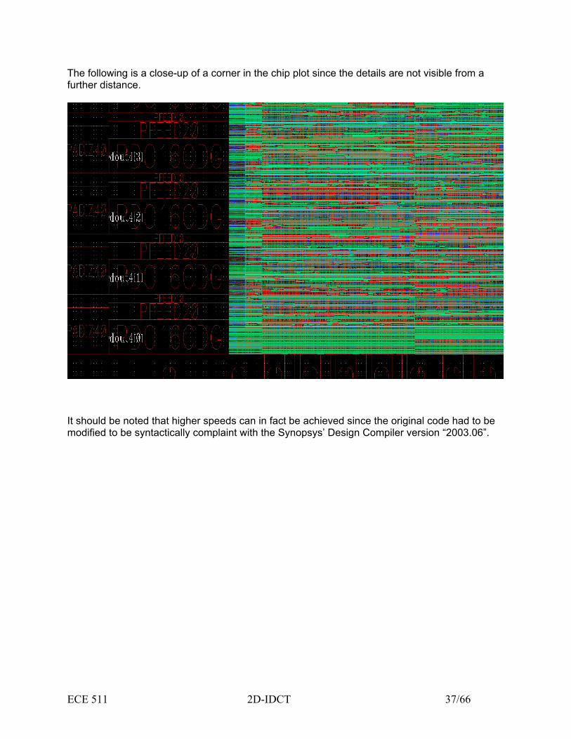
Application Specific Integrated Circuit (ASIC) Results The 2D-IDCT core was modified such that an ASIC version could also be realized. We had taken the core through the design flow and we were able to compile most of the required results. The design was carried through using 0.18 µm CMOS technology files. In regards to the ASIC, three main parameters are of interest: area, power and clock speed. Total Cell Area: 2657860.25 µm2 (equivalent to 1.63 mm2) Minimum Clock Period: 6.49 ns Maximum Clock Frequency: 154 MHz Power Consumption: 643.5 mW The following is a plot of our chip, namely, the IDCT component.
ECE 511 2D-IDCT 37/66
The following is a close-up of a corner in the chip plot since the details are not visible from a further distance.
It should be noted that higher speeds can in fact be achieved since the original code had to be modified to be syntactically complaint with the Synopsys’ Design Compiler version “2003.06”.

ECE 511 2D-IDCT 38/66
Results of Experimentation The complete system simulated successfully. However, systems level testing failed to uncover why an image could not be displayed when written directly to the YcbCr block rams by the IDCT component (although, the 16 x 16 output was successfully being displayed by the VGA controller when initialized in the YCbCr block rams). Furthermore, it was discovered that the IDCT component, was not producing the same values, as produced by the C decoder unit (although it was verified in Matlab, the C decoder program was producing different Y values). A last minute attempt to uncover the reason, by performing an DCT conversion using Matlab, failed to uncover the mysterious system display problem, which was displaying a constant green as a 16 x 16 pixel image. This was also in contrast to the simulated waveform RGB output, where the outputs were shown to being correctly displayed (see simulated waveforms in appendix for System level VGA). The same results, were achieved using two different Xilinx boards, which eliminated the possibility of hardware malfunction, and pointed to a design flaw somewhere in systems integration.

ECE 511 2D-IDCT 39/66
FPGA PINOUT Information Signal Name Signal Type Pin Mapping
(Virtex II Mutimedia)
Description
pixel clock In : std_logic AD16 Pixel clock pixel_clock_out
Out : std_logic
A27 Pixel clock
Blank Out : std_logic
A25 Blanking
Comp Out : std_logic A26 Comp synch R Out :
std_logic_vector(7 downto 0)
E23, E22, H20, H21, B24, B23, D23, D24
Red
G Out : std_logic_vector(7 downto 0)
G21, G22, B25, A24, D25, C24, F22, F23
Green
B Out: std_logic_vector(7 downto 0)
E23, E22, H20, H21, B24, B23, D23, D24
Blue
Table 6: FPGA Pinout Info

ECE 511 2D-IDCT 40/66
References [1] Mihai Sima, Sorin Cotofana, Jos T.J. van Eijndhoven, Stamatis Vassiliadis, Kees A. Vissers,
"An 8x8 IDCT Implementation on an FPGA-augmented TriMedia", in: proc. of IEEE Symp. on Field-Programmable Custom Computing Machines (FCCM 2001), Rohnert Park, California, April-May 2001
[2] Han Bin Kim, Dong Sam Ha, “Design and Synthesis of Built-In Self-Testable Two-
Dimensional Discrete Cosine Transform Circuits”, IEEE, 2000 [3] Color space converter, VGA adapter, Ethernet core, all from the Xilinx corporation -
http://www.xilinx.com/products/boards/multimedia/. Color space converter - XAPP283 (v1.3) July 3, 2003 Xilinx.
[4] JPEG file parser (C code) and documentation - http://www.wotsit.org/download.asp?f=jpeg [5] MicroBlaze development environment (EDK 6.2) and software core from Xilinx Studio
Edition software. [7] Schematic for Micro Blaze Video Board, 10/18/02, Xilinx [8] Tyler Brandon Lee, HDL2GDS program
ECE 511 2D-IDCT 41/66
APPENDIX A: CODE INDEX
GLOBALS_PKG.VHD ................................................................................................................... 42 IDCT_1D_TOP.VHD..................................................................................................................... 43 ROTATOR.VHD ........................................................................................................................... 44 BUTTERFLY.VHD........................................................................................................................ 45 MULTIPLY.VHD.......................................................................................................................... 46 ADD_SUB.VHD ........................................................................................................................... 47 TRANSPOSE_MEMORY.VHD ........................................................................................................ 48 TRANSPOSE_BUFFERS.VHD......................................................................................................... 49 IDCT_DATAPATH.VHD ................................................................................................................ 51 IDCT_CONTROL_UNIT.VHD......................................................................................................... 52 YCBCR_RGB_CONV.VHD.......................................................................................................... 53 GET_RAM_DATA24_256.RGB................................................................................................... 54 SVGATIMINGGENERATION.V ............................................................................................ 55

ECE 511 2D-IDCT 42/66
Globals_pkg.vhd

ECE 511 2D-IDCT 43/66
Idct_1d_top.vhd

ECE 511 2D-IDCT 44/66
Rotator.vhd

ECE 511 2D-IDCT 45/66
Butterfly.vhd

ECE 511 2D-IDCT 46/66
Multiply.vhd

ECE 511 2D-IDCT 47/66
Add_sub.vhd

ECE 511 2D-IDCT 48/66
transpose_memory.vhd

ECE 511 2D-IDCT 49/66
transpose_buffers.vhd

ECE 511 2D-IDCT 50/66
idct_toplevel.vhd

ECE 511 2D-IDCT 51/66
idct_datapath.vhd

ECE 511 2D-IDCT 52/66
idct_control_unit.vhd

ECE 511 2D-IDCT 53/66
YcbCr_RGB_conv.vhd

ECE 511 2D-IDCT 54/66
Get_ram_data24_256.RGB

ECE 511 2D-IDCT 55/66
SVGATIMINGGENERATION.v

ECE 511 2D-IDCT 56/66
APPENDIX B: Testbench and Simulations
TOP_LEVEL_TB.VHD .................................................................................................................. 57 IDCT_1D_TOP_TB.VHD ............................................................................................................... 58 ROTATOR_TB.VHD ..................................................................................................................... 59 BUTTERFLY_TB.VHD.................................................................................................................. 60 MULTIPLY_TB.VHD.................................................................................................................... 61 ADD_SUB_TB.VHD ..................................................................................................................... 62 TRANSPOSE_MEMORY_TB.VHD.................................................................................................. 63 TRANSPOSE_BUFFERS_TB.VHD .................................................................................................. 64 YCBCR_RGB_CONVERTER_TB.VHD ......................................................................................... 65 VGA SYSTEM OUTPUT .............................................................................................................. 66

ECE 511 2D-IDCT 57/66
Top_level_tb.vhd This testbench instantiates the control and data units. Initiates the data flow by setting reset of the control unit.
ECE 511 2D-IDCT 58/66
idct_1d_top_tb.vhd This testbench tests the IDCT conversion values. The inputs are 8 DCT coefficient values, and the outputs are 8 each of Y, Cb, Cr values.

ECE 511 2D-IDCT 59/66
Rotator_tb.vhd This testbench tests the rotator functionality. It provides 2 inputs representing intermediate values in the 1D IDCT, and performs addition, subtraction, sine and cosine multiplying resulting in 2 output values.

ECE 511 2D-IDCT 60/66
Butterfly_tb.vhd This testbench tests the buttefly functionaliy, by performing 2 additions and subtractions.

ECE 511 2D-IDCT 61/66
Multiply_tb.vhd This testbench tests the multiply functionality, by providing two inputs to multiply.

ECE 511 2D-IDCT 62/66
Add_sub_tb.vhd This testbench tests the adder or subtractor functionality of the Add_sub module.

ECE 511 2D-IDCT 63/66
Transpose_memory_tb.vhd This testbench tests the transpose memory functionality.

ECE 511 2D-IDCT 64/66
Transpose_buffers_tb.vhd This testbench tests the transpose_buffers functionality.

ECE 511 2D-IDCT 65/66
YcbCr_RGB_converter_tb.vhd This is a testbench which implements 3 test cases to test the conversion formulas for 8 bit Y,Cb,Cr inputs to 8 bit RGB values

ECE 511 2D-IDCT 66/66
VGA System Output These waveforms show the RGB output, when running behavioral simulations of the completely integrated system, verifying correctness of datapath and control flows.